Embed Size (px)
Citation preview
ni.com/awr
Overview3D electromagnetic (EM) simulators are commonly used to help design board-to-chip transitions. NI AWR Design Environment™ makes
life easier for circuit designers with Analyst™ 3D EM fi nite element method (FEM) simulator. A key advantage of Analyst software is its
tight integration within the Microwave Offi ce circuit design and simulation platform. This application note highlights the unique features of
Analyst by demonstrating the optimization of the transition from a board-to-chip signal path. The example highlights how the ability to
access Analyst from within the Microwave Offi ce environment saves designs time.
Analyst simplifi es layout setup and drawing by offering preconfi gured 3D parametric cells (PCells) for such shapes as bond wires and ball
grid arrays (BGAs). Hierarchy is supported in the EM layout, enabling easier reuse of designs. Tuning, optimization, and sensitivity and
yield analysis can be quickly implemented through the use of parameterized layout, without having to leave the Microwave Offi ce
environment. Since Analyst is optimized for RF designers with automatic simulation settings for typical technologies, users usually do not
need to go into the simulation settings of the software. Designers can now concentrate on their design, easily using 3D EM simulation
when needed, without having to spend time learning a complicated third product tool. Indeed, if they already use AXIEM planar EM
simulation software, they will fi nd Analyst looks almost the same. The learning curve for making effective designs is therefore very short.
Application Note
Design and Optimization of a Board-to-Chip Transition
Board-to-chip transition; layout views, bond wire schematic and cut plane perspectives.
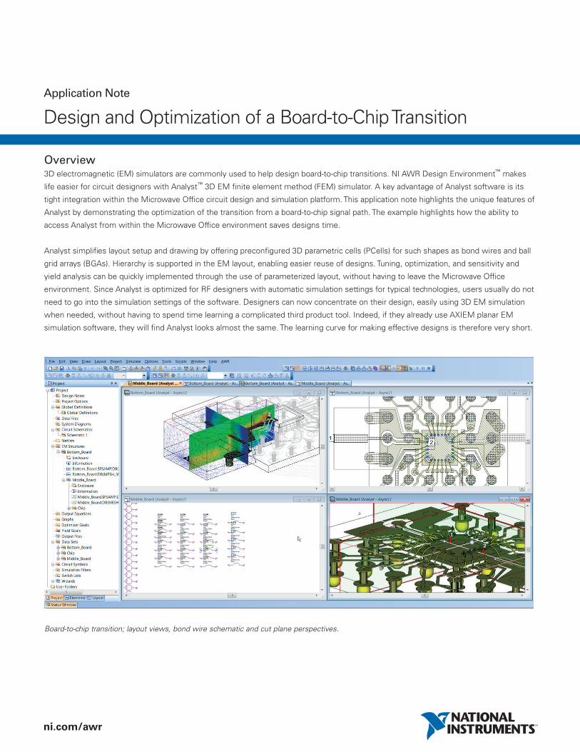
A Board-to-Chip TransitionFigure 1 shows the board, module, and periphery of the chip
being investigated. The signal goes from Port 1 on a trace on a
PC board onto a module by means of a BGA, along a trace on top
of the module, and over to Port 2 on the chip by means of a bond
wire. The design goal is to have a return loss of greater than 20
dB over the frequency range of interest, 10 to 20 GHz.
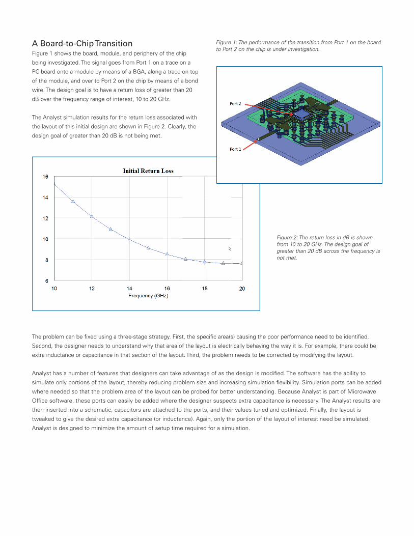
The Analyst simulation results for the return loss associated with
the layout of this initial design are shown in Figure 2. Clearly, the
design goal of greater than 20 dB is not being met.
The problem can be fi xed using a three-stage strategy. First, the specifi c area(s) causing the poor performance need to be identifi ed.
Second, the designer needs to understand why that area of the layout is electrically behaving the way it is. For example, there could be
extra inductance or capacitance in that section of the layout. Third, the problem needs to be corrected by modifying the layout.
Analyst has a number of features that designers can take advantage of as the design is modifi ed. The software has the ability to
simulate only portions of the layout, thereby reducing problem size and increasing simulation fl exibility. Simulation ports can be added
where needed so that the problem area of the layout can be probed for better understanding. Because Analyst is part of Microwave
Offi ce software, these ports can easily be added where the designer suspects extra capacitance is necessary. The Analyst results are
then inserted into a schematic, capacitors are attached to the ports, and their values tuned and optimized. Finally, the layout is
tweaked to give the desired extra capacitance (or inductance). Again, only the portion of the layout of interest need be simulated.
Analyst is designed to minimize the amount of setup time required for a simulation.
Figure 1: The performance of the transition from Port 1 on the board to Port 2 on the chip is under investigation.
Figure 2: The return loss in dB is shown from 10 to 20 GHz. The design goal of greater than 20 dB across the frequency is not met.
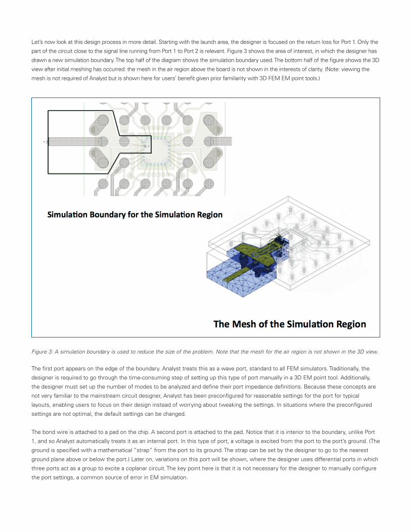
Let’s now look at this design process in more detail. Starting with the launch area, the designer is focused on the return loss for Port 1. Only the
part of the circuit close to the signal line running from Port 1 to Port 2 is relevant. Figure 3 shows the area of interest, in which the designer has
drawn a new simulation boundary. The top half of the diagram shows the simulation boundary used. The bottom half of the fi gure shows the 3D
view after initial meshing has occurred: the mesh in the air region above the board is not shown in the interests of clarity. (Note: viewing the
mesh is not required of Analyst but is shown here for users’ benefi t given prior familiarity with 3D FEM EM point tools.)
The fi rst port appears on the edge of the boundary. Analyst treats this as a wave port, standard to all FEM simulators. Traditionally, the
designer is required to go through the time-consuming step of setting up this type of port manually in a 3D EM point tool. Additionally,
the designer must set up the number of modes to be analyzed and defi ne their port impedance defi nitions. Because these concepts are
not very familiar to the mainstream circuit designer, Analyst has been preconfi gured for reasonable settings for the port for typical
layouts, enabling users to focus on their design instead of worrying about tweaking the settings. In situations where the preconfi gured
settings are not optimal, the default settings can be changed.
The bond wire is attached to a pad on the chip. A second port is attached to the pad. Notice that it is interior to the boundary, unlike Port
1, and so Analyst automatically treats it as an internal port. In this type of port, a voltage is excited from the port to the port’s ground. (The
ground is specifi ed with a mathematical “strap” from the port to its ground. The strap can be set by the designer to go to the nearest
ground plane above or below the port.) Later on, variations on this port will be shown, where the designer uses differential ports in which
three ports act as a group to excite a coplanar circuit. The key point here is that it is not necessary for the designer to manually confi gure
the port settings, a common source of error in EM simulation.
Figure 3: A simulation boundary is used to reduce the size of the problem. Note that the mesh for the air region is not shown in the 3D view.
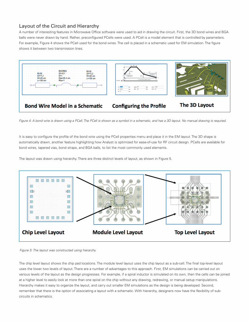
Layout of the Circuit and HierarchyA number of interesting features in Microwave Offi ce software were used to aid in drawing the circuit. First, the 3D bond wires and BGA
balls were never drawn by hand. Rather, preconfi gured PCells were used. A PCell is a model element that is controlled by parameters.
For example, Figure 4 shows the PCell used for the bond wires. The cell is placed in a schematic used for EM simulation. The fi gure
shows it between two transmission lines.
It is easy to confi gure the profi le of the bond wire using the PCell properties menu and place it in the EM layout. The 3D shape is
automatically drawn, another feature highlighting how Analyst is optimized for ease-of-use for RF circuit design. PCells are available for
bond wires, tapered vias, bond straps, and BGA balls, to list the most commonly used elements.
The layout was drawn using hierarchy. There are three distinct levels of layout, as shown in Figure 5.
The chip level layout shows the chip pad locations. The module level layout uses the chip layout as a sub-cell. The fi nal top-level layout
uses the lower two levels of layout. There are a number of advantages to this approach. First, EM simulations can be carried out on
various levels of the layout as the design progresses. For example, if a spiral inductor is simulated on its own, then the cells can be joined
at a higher level to easily look at more than one spiral on the chip without any drawing, redrawing, or manual setup manipulations.
Hierarchy makes it easy to organize the layout, and carry out smaller EM simulations as the design is being developed. Second,
remember that there is the option of associating a layout with a schematic. With hierarchy, designers now have the fl exibility of sub-
circuits in schematics.
Figure 4: A bond wire is drawn using a PCell. The PCell is shown as a symbol in a schematic, and has a 3D layout. No manual drawing is required.
Figure 5: The layout was constructed using hierarchy.
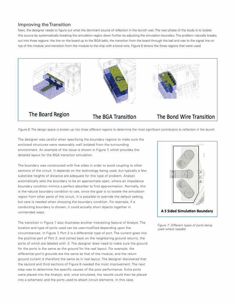
Improving the TransitionNext, the designer needs to fi gure out what the dominant source of refl ection in the launch was. The next phase of the study is to isolate
this source by systematically breaking the simulation region down further by adjusting the simulation boundary. The problem naturally breaks
out into three regions: the line on the board up to the BGA balls; the transition from the board through the ball and vias to the signal line on
top of the module; and transition from the module to the chip with a bond wire. Figure 6 shows the three regions that were used.
The designer was careful when specifying the boundary regions to make sure the
enclosed structures were reasonably well isolated from the surrounding
environment. An example of the issue is shown in Figure 7, which provides the
detailed layout for the BGA transition simulation.
The boundary was constructed with five sides in order to avoid coupling to other
sections of the circuit. It depends on the technology being used, but typically a few
substrate heights of distance are adequate for this type of problem. Analyst
automatically sets the boundary to be an approximate open, where an impedance
boundary condition mimics a perfect absorber to first approximation. Normally, this
is the natural boundary condition to use, since the goal is to isolate the simulation
region from other parts of the circuit. It is possible to override the default setting,
but care is needed when choosing the boundary condition. For example, if a
conducting boundary is chosen, it could actually short objects together in
unintended ways.
The transition in Figure 7 also illustrates another interesting feature of Analyst. The
location and type of ports used can be user-modified depending upon the
circumstances. In Figure 7, Port 2 is a differential type of port. The current goes into
the positive part of Port 2, and comes back on the neighboring ground returns, the
ports of which are labeled with -2. The designer does need to make sure the ground
for the ports is the same as the ground for the real layout. For example, the
differential port’s grounds are the same as that of the module, and the return
ground current is therefore the same as in real layout. The designer discovered that
the second and third sections of Figure 6 needed the most improvement. The next
step was to determine the specific causes of the poor performance. Extra ports
were placed into the Analyst, and, once simulated, the results could then be placed
into a schematic and the ports used to attach circuit elements. In this case,
Figure 6: The design space is broken up into three different regions to determine the most significant contributors to reflection in the launch.
Figure 7: Different types of ports being used where needed.
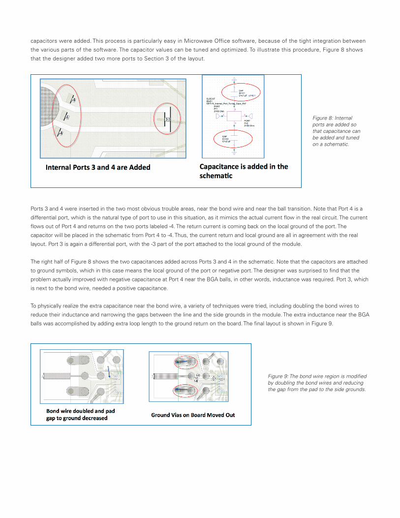
capacitors were added. This process is particularly easy in Microwave Office software, because of the tight integration between
the various parts of the software. The capacitor values can be tuned and optimized. To illustrate this procedure, Figure 8 shows
that the designer added two more ports to Section 3 of the layout.
Ports 3 and 4 were inserted in the two most obvious trouble areas, near the bond wire and near the ball transition. Note that Port 4 is a
differential port, which is the natural type of port to use in this situation, as it mimics the actual current fl ow in the real circuit. The current
fl ows out of Port 4 and returns on the two ports labeled -4. The return current is coming back on the local ground of the port. The
capacitor will be placed in the schematic from Port 4 to -4. Thus, the current return and local ground are all in agreement with the real
layout. Port 3 is again a differential port, with the -3 part of the port attached to the local ground of the module.
The right half of Figure 8 shows the two capacitances added across Ports 3 and 4 in the schematic. Note that the capacitors are attached
to ground symbols, which in this case means the local ground of the port or negative port. The designer was surprised to fi nd that the
problem actually improved with negative capacitance at Port 4 near the BGA balls, in other words, inductance was required. Port 3, which
is next to the bond wire, needed a positive capacitance.
To physically realize the extra capacitance near the bond wire, a variety of techniques were tried, including doubling the bond wires to
reduce their inductance and narrowing the gaps between the line and the side grounds in the module. The extra inductance near the BGA
balls was accomplished by adding extra loop length to the ground return on the board. The fi nal layout is shown in Figure 9.
Figure 8: Internal ports are added so that capacitance can be added and tuned on a schematic.
Figure 9: The bond wire region is modified by doubling the bond wires and reducing the gap from the pad to the side grounds.
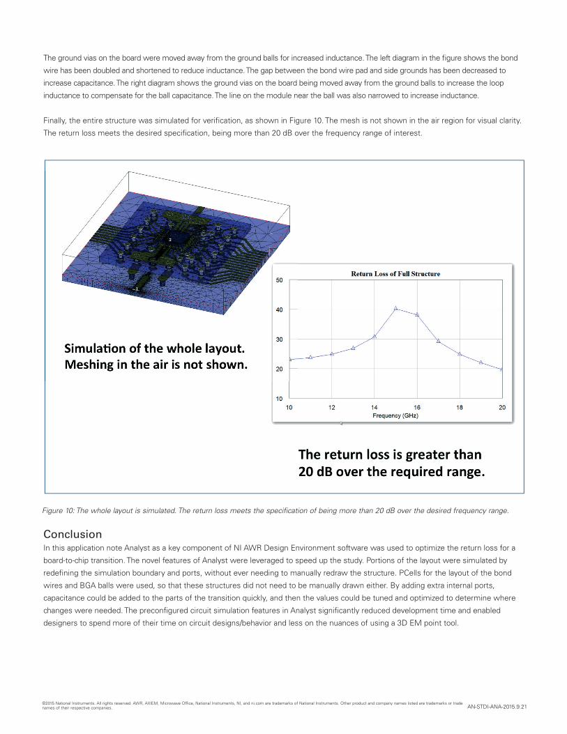
The ground vias on the board were moved away from the ground balls for increased inductance. The left diagram in the fi gure shows the bond
wire has been doubled and shortened to reduce inductance. The gap between the bond wire pad and side grounds has been decreased to
increase capacitance. The right diagram shows the ground vias on the board being moved away from the ground balls to increase the loop
inductance to compensate for the ball capacitance. The line on the module near the ball was also narrowed to increase inductance.
Finally, the entire structure was simulated for verifi cation, as shown in Figure 10. The mesh is not shown in the air region for visual clarity.
The return loss meets the desired specifi cation, being more than 20 dB over the frequency range of interest.
ConclusionIn this application note Analyst as a key component of NI AWR Design Environment software was used to optimize the return loss for a
board-to-chip transition. The novel features of Analyst were leveraged to speed up the study. Portions of the layout were simulated by
redefi ning the simulation boundary and ports, without ever needing to manually redraw the structure. PCells for the layout of the bond
wires and BGA balls were used, so that these structures did not need to be manually drawn either. By adding extra internal ports,
capacitance could be added to the parts of the transition quickly, and then the values could be tuned and optimized to determine where
changes were needed. The preconfi gured circuit simulation features in Analyst signifi cantly reduced development time and enabled
designers to spend more of their time on circuit designs/behavior and less on the nuances of using a 3D EM point tool.
©2015 National Instruments. All rights reserved. AWR, AXIEM, Microwave Offi ce, National Instruments, NI, and ni.com are trademarks of National Instruments. Other product and company names listed are trademarks or trade names of their respective companies. AN-STDI-ANA-2015.9.21
Figure 10: The whole layout is simulated. The return loss meets the specification of being more than 20 dB over the desired frequency range.