Embed Size (px)
Citation preview

XAPP866 (v3.0) April 7, 2008 www.xilinx.com 1
© 2007–2008 Xilinx, Inc. All rights reserved. XILINX, the Xilinx logo, and other designated brands included herein are trademarks of Xilinx, Inc. All other trademarks are the property of their respective owners.
Summary This application note describes how to interface a Texas Instruments analog-to-digital converter (ADC) with serial low-voltage differential signaling (LVDS) outputs to Virtex™-4 or Virtex-5 FPGAs, utilizing the dedicated deserializer functions of both FPGA families. This application note and its two reference designs also illustrate a basic LVDS interface for connecting to any ADC converter with high-speed serial interfaces. Reference solutions are provided to connect ADCs to all Virtex FPGA families.
Introduction Texas Instruments provides a family of high-speed ADCs with serial LVDS interfaces. ADCs are available with:
• 1 to 4 channels
• 12, 14, or 16 bits of resolution
• Speeds of up to 125 Megasamples per second (MSPS)
In addition, these ADCs feature a serial programming interface (SPI) for controlling how data is presented.
This application note and its two reference designs utilize a DDR bit clock with a 12-bit or 16-bit serialization factor for the data. Both single-wire and dual-wire interfaces are discussed. Each of the interfaces has its advantages:
• Using a one-wire interface consumes less I/O (only one LVDS pair per ADC data output).
• Using a two-wire interface allows for higher sample rate converters to be connected.
The two reference designs, which accompany this application, use these interfaces:
• Classic ADC interface: This interface can be used for ADC devices used in one-wire mode. The Virtex-4 and Virtex-5 FPGA I/O features are not used, and the complete deserializer is designed within the FPGA logic. This interface is similar to the interface used in the Connecting Xilinx FPGAs to Texas Instruments ADS527x Series ADCs application note. [Ref 1]
• Featured ADC interface: This reference design supports both one-wire and two-wire interfaces. It uses the Virtex-4 and Virtex-5 FPGA I/O features. The deserializer is implemented using the ISERDES component and regional clocking options of Virtex-4 and Virtex-5 FPGAs.
The two reference designs support multi-channel ADCs with resolutions of 12, 14, or 16 bits, and sampling speeds of up to 125 MSPS. The modular design approach taken allows the design to be easily modified to support higher resolutions and/or a different number of channels.
Application Note: Virtex-4 and Virtex-5 FPGAs
XAPP866 (v3.0) April 7, 2008
An Interface for Texas InstrumentsAnalog-to-Digital Converters with Serial LVDS OutputsAuthor: Marc Defossez
R

LVDS Interface
XAPP866 (v3.0) April 7, 2008 www.xilinx.com 2
R
LVDS Interface Many ADCs use a serialized LVDS interface in which the data is provided over one or two LVDS channels. Digital data is output with a high-speed bit clock and a frame signal. Figure 1 shows the analog input signal along with the input, bit, and frame clock. The frequency of the high-speed bit rate clock is determined by the resolution and sample rate of the ADC.
The maximum speed of the LVDS I/O is set by the maximum possible speed of the clock toggling the flip-flops in the FPGA logic or the ISERDES components. Therefore, the maximum sample speed of a single-channel LVDS ADC device with one-wire interface is limited.
The bit clock rate for single-channel ADC devices in one-wire DDR mode is represented by Equation 1.
Equation 1
For a 16-bit, 125 MSPS device, the equation is (16 × 125)/2 = 1000 MHz, which equals a bit rate of 2 Gb/s. These bit and clock rates are too high for LVDS I/O in any FPGA speed grade.
The two-wire interface offers a solution to this speed barrier by using two data channels per ADC. This technique doubles the data throughput rate as shown in Equation 2.
Equation 2
When the single-channel, 16-bit, 125 MSPS ADC device is used in two-channel mode, the bit clock rate becomes 500 MHz, making it possible to connect these high-speed ADC devices to the FPGA.
X-Ref Target - Figure 1
Figure 1: Single-Channel Converter Setup
SampleN
X866_01_010908
InputSignal
InputClock
CLKM
Latency Clocks
Sample N-1 Sample N
D11 D10 D9 D8 D7 D6 D5 D4 D3 D2 D1 D0 D9 D8 D7 D6 D5 D4 D3 D2 D1 D0D11 D10
TS = 1 Þ FS
CLKP
FCLK_M
FCLK_P
DCLK_P
DCLK_M
DX_P
DX_M
BitClock
FrameClock
OutputData
tA
ADC_resolution Sample_rate×2
------------------------------------------------------------------------------------- bit_clock MHz( )=
ADC_resolution( ) 2⁄ Sample_rate×2
------------------------------------------------------------------------------------------------- bit_clock MHz( )=

LVDS Interface
XAPP866 (v3.0) April 7, 2008 www.xilinx.com 3
R
Figure 2 shows the timing diagram of a 14/16-bit resolution ADC with a one-wire interface, and Figure 3 shows the same ADC with a two-wire interface. Data can be transmitted by the ADC over the LVDS channel with either the most significant bit (MSB) or the least significant bit (LSB) first and with bit or byte alignment.
As mentioned previously, the one-wire interface encounters speed problems sooner than the two-wire interface.
The classic ADC interface version of the one-wire reference design can support any number of resolution bits up to 80 MSPS because the serializer is constructed inside the FPGA logic (slices and flip-flops) and uses a digital clock manager (DCM) as the internal clock source. However, the featured ADC interface is limited to 12-bit resolution and approximately 120 MSPS because it is bonded to the ISERDES components.
The two-wire reference design (featured ADC interface) supports ADCs with sampling resolutions of 12, 14, or 16 bits, and sampling speeds of up to 125 MSPS for 16 bits. The modular design approach of both reference designs allows for easy modification to support higher resolutions and/or a different number of channels.
X-Ref Target - Figure 2
Figure 2: 14/16-Bit ADC and 1-Wire, 4x Bit Clock Output Waveform
Sample N
Data Bit in MSB First Mode
Data Bit in LSB First Mode
Input ClockCLKP
Frame ClockFCLKP at 1X
Bit Clock 8XDCLKP16X
SerialFactor Output Data
DX_P, DX_MD12(D3)
D11(D4)
D10(D5)
D9(D6)
D8(D7)
D7(D8)
D6(D9)
D5(D10)
D4(D11)
D3(D12)
D2(D13)
D1(0)
D0(0)
0(D0)
0(D1)
D13(D2)
D13(D2)
0(D1)
0(D0)
SampleN+1
X866_02_021308
X-Ref Target - Figure 3
Figure 3: 14/16-Bit ADC and 2-Wire, 4x Bit Clock Output Waveform
FCLK
DCLK
Dx0P, Dx0MD1
(D6)D0
(D7)D7
(D0)D6
(D1)D3
(D4)D2
(D5)D1
(D6)D0
(D7)D5
(D2)D4
(D3)D7
(D0)D6
(D1)
D9(0)
D8(0)
0(D8)
0(D9)
D11(D12)
D10(D13)
D9(0)
D8(0)
D13(D10)
D12(D11)
D0(D8)
D0(D9)
D2(D12)
D0(0)
0(D0)
D12(D2)
D6(D8)
D4(D10)
D2(D12)
D0(0)
D10(D4)
D8(D6)
D9(D14)
D8(0)
0(D8)
D13(D9)
D7(D12)
D5(D13)
D3(D14)
D1(0)
D11(D10)
D9(D11)
0(D0)
D12(D2)
0(D8)
D14(D9)
Byte WiseMode
Bit WiseMode
Dx1P, Dx1M
Dx0P, Dx0M
Dx1P, Dx1M
X866_03_021308

Virtex-4 and Virtex-5 FPGA I/O Architecture
XAPP866 (v3.0) April 7, 2008 www.xilinx.com 4
R
All ADC settings can be controlled and programmed through a serial (SPI) or parallel interface. The SPI interface is not discussed in this application note. However, each reference design includes a sample design that connects the FPGA over a UART-USB link with a PC capable of programming the ADC using SPI.
Virtex-4 and Virtex-5 FPGA I/O Architecture
This section highlights architectural comparisons between Virtex-4 and Virtex-5 FPGAs as they apply to the application. Consult the specific device user guides for additional information. [Ref 2], [Ref 3]
IOBVirtex-4 and Virtex-5 devices share a similar I/O block (IOB) structure. The IOBs of both architectures contain only input and output (3-state) buffers (Figure 4).
Two IOBs can be paired together to form a differential input or output. These inputs and outputs to the FPGA logic are controlled by ISERDES (ILOGIC) and OSERDES (OLOGIC). Figure 5 illustrates the inputs and outputs and how the IOB pair is used in the reference design.
X-Ref Target - Figure 4
Figure 4: Virtex-4 and Virtex-5 FPGA IOB
X-Ref Target - Figure 5
Figure 5: I/O Structure of Virtex-4 and Virtex-5 FPGAs
X866_04_012108
IBUF
OBUF,OBUFT
T
I
O
IO
IOBUF
X866_05_011608
P_PAD
IB
I
O
OB
N_PAD
IBUFDS_DIFF_OUT
ILOGICISERDES
OLOGICOSERDES
IODELAY
ILOGICISERDES
OLOGICOSERDES
IODELAY
Rou
ting
Con
nect
ions
Rou
ting
Con
nect
ions

Virtex-4 and Virtex-5 FPGA I/O Architecture
XAPP866 (v3.0) April 7, 2008 www.xilinx.com 5
R
IDELAY, IODELAY, and ISERDES
Virtex-4 devices only have IDELAY (no IODELAY), which is integrated in ISERDES as shown in Figure 6. As such, IODELAY in Figure 5 is replaced by IDELAY in terms of Virtex-4 devices. Virtex-5 devices have IODELAY, and the setup is exactly as shown in Figure 5.
In Virtex-5 devices, the IODELAY component (Figure 7) is not part of ISERDES because IODELAY must also be available for use with OSERDES. IODELAY must be instantiated along with the ISERDES_NODELAY primitive.
IDELAY/IODELAY can be used independently or in combination with ISERDES for both Virtex-4 and Virtex-5 FPGA technologies. In Virtex-4 FPGAs, the operating mode of IDELAY is configured by setting the appropriate attributes in the HDL instantiation model of ISERDES.
X-Ref Target - Figure 6
Figure 6: ISERDES of Virtex-4 FPGA with IDELAY
DLYINCDLYCE
DLYRST
D
IDELAY
SHIFTIN1 SHIFTIN2
SHIFTOUT1 SHIFTOUT2
BITSLIP
OCLKCE1CE2
SRREV
BITSLIP
O
Q1Q2Q3Q4Q5Q6
CLKCLKDIV
X866_07_012808

Virtex-4 and Virtex-5 FPGA I/O Architecture
XAPP866 (v3.0) April 7, 2008 www.xilinx.com 6
R
Figure 8 shows the four configurations of IDELAY (for Virtex-4 FPGAs) or IODELAY (for Virtex-5 FPGAs). These functions are done by configuration for Virtex-4 FPGAs and by FPGA routing for Virtex-5 FPGAs.
X-Ref Target - Figure 7
Figure 7: Virtex-5 IODELAY with ISERDES_NODELAY
D
SHIFTIN1 SHIFTIN2
SHIFTOUT1 SHIFTOUT2
BITSLIP
OCLKCE1CE2RST
CLK
BITSLIP
Q1
DATAOUT
Q2Q3Q4Q5Q6
CLKBCLKDIV
IDATAINDATAIN
ODATAINT
INCCE
RSTC
IODELAY
X866_07_021308
DATAIN = Input from FPGA LogicODATAIN = Input from OLOGIC.O
X-Ref Target - Figure 8
Figure 8: IDELAY or IODELAY Possible Configurations
To ISERDES Flip-flops
Configuration 1
Configuration 3 Configuration 4
Configuration 2
D ONONE
To ISERDES Flip-flops
To ISERDES Flip-flops
To ISERDES Flip-flops
D OIBUF
D OBOTH
D OIFD
X866_08_011808

Virtex-4 and Virtex-5 FPGA I/O Architecture
XAPP866 (v3.0) April 7, 2008 www.xilinx.com 7
R
The four possible configurations of IDELAY or IODELAY are:
• Configuration 1: IDELAY/IODELAY is not used, and the input signal connects directly to the ISERDES flip-flops, internal slice flip-flops, or logic.
• Configuration 2: IDELAY/IODELAY is used to delay the input signal path to the slice flip-flops or logic. The input signal connects directly to the ISERDES flip-flops.
• Configuration 3: IDELAY/IODELAY is used to delay the input signal for both the ISERDES flip-flops and internal slice flip-flops or logic.
• Configuration 4: IDELAY/IODELAY is used to delay the input signal path to the ISERDES flip-flops. The input signal connects directly to the slice flip-flops or logic.
IDELAY and IODELAY can be used in variable delay or fixed delay mode. The delay chain consists of 64 taps of 78 ps (IDELAYCTRL is clocked at 200 MHz).
Virtex-4 FPGA designs using ISERDES devices can be implemented using Virtex-5 devices without modifications to the HDL code. Xilinx ISE™ software provides a seamless migration path for the components. For more information regarding IDELAY or IODELAY, refer to the appropriate device user guides listed in “Additional Resources,” page 30.
Clock Buffers
The clock buffers available in Virtex-4 and Virtex-5 devices are part of the regional clocking solutions. Figure 9 shows an example clock connection scheme. Refer to the appropriate family user guides for application guidelines. [Ref 2], [Ref 3]
BUFIO
The BUFIO clock buffer must be driven by a clock-capable I/O and supports a dedicated clock network. This network can only be used to clock the I/O components ISERDES and OSERDES, and derivatives.
In Virtex-4 devices, two BUFIOs are available per I/O bank. These buffers can drive I/O resources in their own regions and in the two adjacent regions. In Virtex-5 devices, four BUFIOs are available per I/O bank. These buffers support only clocking of I/O resources in their own regions.
BUFR
The BUFR clock buffer can drive I/O resources and all logic in its region independently of the global clock solutions and can generate a divided clock.
X-Ref Target - Figure 9
Figure 9: Regional Clock Solutions in Virtex-4 and Virtex-5 Devices
X866_06_011008
BUFR
From ClockCapable I/O
To I/O Resources inthis Region and in the
Adjacent Region
To I/O Resources inthis Region and in the
Adjacent Region
To I/O and LogicResources in thisRegion and in theAdjacent Region
To I/O and LogicResources in thisRegion and in theAdjacent Region
BUFIO
Virtex-4 Device
BUFRFrom ClockCapable I/O
To I/O Resources inthis Region
To I/O Resources inthis Region
To I/O and LogicResources
in this Region
To I/O and LogicResources
in this Region
BUFIO
Virtex-5 Device
Classic ADC Interface
XAPP866 (v3.0) April 7, 2008 www.xilinx.com 8
R
In Virtex-4 devices, two BUFRs are available per I/O bank. These buffers have clock capabilities in their own region and in the two adjacent regions. They are driven from the BUFIO output on the local interconnect.
In Virtex-5 devices, two BUFRs are available per I/O bank, supporting clocking only in their own region. Virtex-5 FPGA BUFRs can be driven by a clock-capable I/O or from the local interconnect.
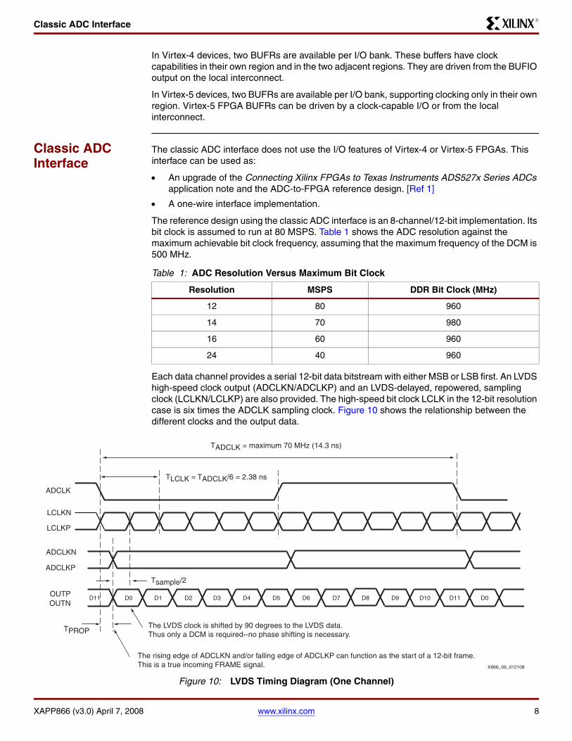
Classic ADC Interface
The classic ADC interface does not use the I/O features of Virtex-4 or Virtex-5 FPGAs. This interface can be used as:
• An upgrade of the Connecting Xilinx FPGAs to Texas Instruments ADS527x Series ADCs application note and the ADC-to-FPGA reference design. [Ref 1]
• A one-wire interface implementation.
The reference design using the classic ADC interface is an 8-channel/12-bit implementation. Its bit clock is assumed to run at 80 MSPS. Table 1 shows the ADC resolution against the maximum achievable bit clock frequency, assuming that the maximum frequency of the DCM is 500 MHz.
Each data channel provides a serial 12-bit data bitstream with either MSB or LSB first. An LVDS high-speed clock output (ADCLKN/ADCLKP) and an LVDS-delayed, repowered, sampling clock (LCLKN/LCLKP) are also provided. The high-speed bit clock LCLK in the 12-bit resolution case is six times the ADCLK sampling clock. Figure 10 shows the relationship between the different clocks and the output data.
Table 1: ADC Resolution Versus Maximum Bit Clock
Resolution MSPS DDR Bit Clock (MHz)
12 80 960
14 70 980
16 60 960
24 40 960
X-Ref Target - Figure 10
Figure 10: LVDS Timing Diagram (One Channel)
TPROP
Tsample/2
TLCLK = TADCLK/6 = 2.38 ns
TADCLK = maximum 70 MHz (14.3 ns)
The LVDS clock is shifted by 90 degrees to the LVDS data.Thus only a DCM is required--no phase shifting is necessary.
The rising edge of ADCLKN and/or falling edge of ADCLKP can function as the start of a 12-bit frame.This is a true incoming FRAME signal.
D0 D0D10 D11D1D11 D2 D3 D4 D5 D6 D7 D8 D9
ADCLK
LCLKP
LCLKN
ADCLKP
ADCLKN
OUTPOUTN
X866_09_012108

Classic ADC Interface
XAPP866 (v3.0) April 7, 2008 www.xilinx.com 9
R
A set of registers in the ADC can be read or written through an SPI/Microwire (I2C look-alike) protocol. The SPI/Microwire protocol and its FPGA implementation are not discussed in this application note. An example design using a PicoBlaze™ processor is available with the featured design. Free, adaptable designs can be downloaded from the Internet.
Bit Clock
As shown in Figure 11, the ADC transmits data and frame/sync 90° out of phase with respect to the bit clock. In this design, the ADC bit clock is connected to global clock inputs of the FPGA while data and frame signals are connected to a regular I/O bank. Therefore, it is strongly recommended that all PCB traces between the ADC and FPGA have the same length to preserve the original phase shift to the FPGA.
A DCM and a state machine ensure that the exact phase relationship between the signals of the ADC is maintained inside the FPGA grid, i.e., the bit clock (LCLK) is exactly positioned in the middle of the received data bit width. All IOBs (from PAD to ISERDES.D input) are the same and have the same timing parameters. The IOBs acting as clock inputs use a direct connect routing to the DCM clock input, but the normal IOB and ISERDES logic can still be used. The classic ADC reference design provides the ability to use the IOB and ISERDES functionalities when routing a clock via the direct routes to a DCM.
In the circuit shown in Figure 11, the incoming clock is used as the clock input for the DCM and as the data input for the IOB flip-flop. The input clock registers itself at the IOB flip-flop with the DCM-adjusted clock (ClkIn). The DCM is set in variable phase shift mode with an initial phase shift of –255. The equivalent counter in the control logic is set to 0, as is the internal state machine.
When taken out of reset, the DCM adjusts its output clocks to the incoming bit clock and indicates this adjustment process with the LOCKED output. The external and internal clocks are phase aligned.
X-Ref Target - Figure 11
Figure 11: DCM Phase Adjustment
PS
EN
CLK0CLK90
CLK180CLK270CLK2X
CLK2X180CLKDVCLKFX
CLKFX180
DCM
ControlLogic
IOB
LOCKED
PSDONE
PSDONE
PS
CLK
PS
INC
LOCKIN
CLKIN
ClkIn
ClkInNot
DATIN
K CONSTANTLOCKOUT
PHASEVAL
PSINCDECPSENPSCLK
CLKINCLKFB
RSTDSSEN
STATUS[7:0]
D Q
X866_10_011108

Classic ADC Interface
XAPP866 (v3.0) April 7, 2008 www.xilinx.com 10
R
The DCM phase shift is then incremented with the state machine, and a counter in the state machine is incremented by the PSDONE signal from the DCM. The output of the IOB flip-flop is checked and shows a stable value, e.g., 0. Incrementing continues until the input flip-flop value becomes 1. The counter value (PosCnt_0) at this point indicates the setup time to the rising edge of the input clock, via the flip-flop, with respect to the corrected clock. The phase continues to be increased, and at some point, the IOB register changes back to 0. This point effectively corresponds to the setup time of the falling edge of the input clock, via the register, with respect to the corrected clock. This point can be called PosCnt_1.
Next, the value PosCnt_2 (PosCnt_1 – PosCnt_0) is calculated. The DCM is then decremented until its value is PosCnt_2. Setup is finished. The LOCKOUT output of the state machine is driven High. The LOCKOUT output performs the same function as the LOCKED output of the DCM and indicates that the startup of the DCM is finished.
When using auto-phase shift correction without precautions, the initial 90° phase shift that the ADC applies to the bit clock can be lost. The DCM moves the clock edge (after adjustment by the control logic) in the middle of a half-clock period, reducing the phase shift between clock and data to zero. The fixed value K must be applied to the state machine to ensure that a phase shift of 90° is established. The value K is a constant applied in the HDL code.
Frame Clock
The frame clock is used as a strobe signal to capture data words in a parallel register. The frame clock signal is sampled on the positive and negative edges of the bit clock. When the frame signal changes from Low to High, a full ADC word is available in the deserializer register and a new ADC word starts. A small state machine performs edge and phase detection. The frame state machine signals are shown in Figure 12.
X-Ref Target - Figure 12
Figure 12: Frame State Machine Signals
Rising Edge First
Clk
Clock Rising EdgeParallel Register Clock Falling Edge
Parallel Register
FrameIDDR Q0
IDDR Q1
AdcFrmEnaMuxP
AdcFrmEnaMuxN
AdcFrmMuxEna
Falling Edge First
Clk
Clock Falling EdgeParallel Register Clock Rising Edge
Parallel Register
FrameIDDR Q0
IDDR Q1
AdcFrmEnaMuxP
AdcFrmEnaMuxN
AdcFrmMuxEna
X866_12_011008

Classic ADC Interface
XAPP866 (v3.0) April 7, 2008 www.xilinx.com 11
R
When a rising edge of the frame is detected, enable signals are generated to store positive and negative clocked data in parallel storage registers. The same state machine then provides the enable signals for the bit swap multiplexer and block RAM storage.
Normally, even bits (0, 2, ..., 10) are clocked on the rising edge of the DCM-aligned bit clock (ClkIn), while odd bits (1, 3, …, 11) are clocked on the falling edge of that clock. However, it is possible for the falling edge to arrive first and clock the even data in the odd data shift register and clock the odd data in the even data shift register.
At the rising edge of the frame clock, two signals are generated to enable the parallel storage registers for the positive and negative clocked data.
The frame state machine must provide the correct enable for the correct parallel storage register and then set the bit swap multiplexer so that the bits from the ADC are properly aligned for storage in the block RAM or look-up table (LUT) RAM.
Data
Data is captured on rising and falling edges of the bit clock. A complete ADC word is shifted into the deserializer register when a rising frame edge is detected. This word must be transported into a parallel register, allowing for a new serial word to be shifted into the deserializer.
The assumption is that a rising edge of the bit clock captures the even data bits and a falling edge of that clock captures the odd bits. In reality it is never known when and at what edge of the bit clock that data is captured. It is possible that the falling edge of the bit clock captures even data bits in the register for odd data and vice versa (Figure 13). The frame state machine ensures that the bits are clocked at the right moment. The frame state machine also provides a signal that sets a bit swap multiplexer for correct alignment of the data bits.
Figure 14 shows a one-channel data capture module. This module outputs the serial differential data of one channel, internal to the FPGA, as ADC resolution-wide parallel data.
The data capture module can be used several times, and the deserializer depth can be adjusted. A deserializer of 24 bits and more can be constructed.
Data is presented in DDR format, meaning that it must be clocked into the receiver registers on the rising and falling edges of the bit clock. To do this, the IDDR (OPPOSITE_EDGE) setup of the ISERDES is used. The data is thus delayed by one bit clock cycle. Clocking the incoming serial data bits of a channel with the positive and negative bit clock edges in different registers
X-Ref Target - Figure 13
Figure 13: Data Bit Order following the Bit Clock Edge
X866_13_011308
C
D B T
A S C
D
0
B T
A S
IDDR (Opposite Edge)
Data
Frame
Clk
MUX
Q0
Q1
C B A T S R
D
C A S
B T C
D
1
B T
A SData
Frame
Clk
Q0
Q1
C B A T S R

Featured ADC Interface
XAPP866 (v3.0) April 7, 2008 www.xilinx.com 12
R
is equivalent to splitting data frames into two sections. Each section is a serial-to-parallel shift register. At a strobe pulse from the frame clock, the serial register bits are stored in a parallel register. The result is a parallel word with possible jumbled data bit order. After the bit ordering is resolved by the multiplexer, the parallel word can be fed to a set of registers, LUT-based RAM, a block RAM buffer/FIFO, or a block RAM used as a register.
The data capturing design runs at the high-speed bit clock. The design uses RLOC constraints to ensure that the maximum possible speed is always achieved. RLOC constraints are also used to position hierarchical levels with respect to each other in the FPGA logic. These constraints are placed in the HDL code.
The reference designs include a spreadsheet file titled XC5VLX50T-FF1136.xls that shows the layout of the logic region interface in a Virtex-5 FPGA I/O bank. By means of generic HDL parameters, the interface can be placed anywhere in the FPGA.
Featured ADC Interface
This section describes the reference design that implements the featured ADC interface.
Bit Clock
The bit clock rate for single-channel ADC devices in one-wire, DDR mode is again represented by Equation 1. For a 16-bit, 125 MSPS device, the equation is (16 × 125)/2 = 1000 MHz, which equals a bit rate of 2 Gb/s. These bit and clock rates are too high for LVDS I/O in any FPGA speed grade.
The two-wire interface offers a solution to this speed barrier by using two data channels per ADC. This technique doubles the data throughput rate, as shown in Equation 2.
Following the example, when the single-channel, 14-bit, 125 MSPS ADC device is used in two-channel mode, the bit clock rate becomes 437.5 MHz, making it possible to connect these high-speed ADC devices to the FPGA.
X-Ref Target - Figure 14
Figure 14: Single Channel Data Capturing Module
Register,LUT RAM, orBlock RAM
Memory
Flip-FlopCascade
Frame StateMachine
DCM AdjustState Machine
Clk
DCM
IDDRIBUFDS
X866_14_022808
IBUFDS
IBUFGDS
Flip-FlopCascade
EnaRegClk0
EnaRegClk180
EnaBitSwapMux
EnaMemory
Reg
iste
r
Bit
Sw
ap M
ultip
lexe
r
Reg
iste
r

Featured ADC Interface
XAPP866 (v3.0) April 7, 2008 www.xilinx.com 13
R
The output mode of the ADC can be set statically via pull-up and pull-down resistors or dynamically through the ADC’s SPI interface. For the featured ADC interface reference design, the ADC is set to two-wire mode. To align the 14 data bits into a 16-bit word, the remaining bits are stuffed with 0s.
The bit clock provided by the ADC is 90° out of phase with respect to data and frame signals. In addition, the delay from the package pad to the D input of each ISERDES is equal for all signals.
Bit-Clock Alignment
This reference design does not use a DCM, but it adopts the principle of phase shifting to align the bit clock from the DCM implementation.
When a bit is routed through a clock-capable I/O, BUFIO, and/or BUFR clock buffer, it receives a different amount of delay than the data and frame signals. The phase relationship between the signals gets lost. To compensate, the bit clock must be realigned to the data and frame signals.
The signal path from the die pad into the ISERDES devices used to capture data is identical for all I/Os. Data, frame, and bit clock have the same PAD-to-ISERDES delay, and each ISERDES has the same timing specifications. Consequently, when the bit clock, the data, and the frame signals can be captured by a delay-adjusted version of the bit clock, it is possible to have the signals aligned internally, as on the FPGA package input pins.
Basic Bit-Clock Alignment Operation
This section explains the bit-clock alignment principle for a Virtex-4 FPGA integration. The bit clock (DCLK) from the ADC is routed through IDELAY, BUFIO, and BUFR (Figure 15). When the clock passes through IDELAY and the clock buffers, it accumulates a time delay when arriving at the CLK (ClkCtrl_MonClk) and CLKDIV (ClkCtrl_RefClk) inputs of the same ISERDES used for passing the clock through IDELAY.

Featured ADC Interface
XAPP866 (v3.0) April 7, 2008 www.xilinx.com 14
R
The input clock at the ISERDES.D input (ClkCtrl_InClk) is also directly applied to the internal deserializer of ISERDES. As a result, the delayed versions of the DCLK (ClkCtrl_Mon and ClkCtrl_RefClk) are used to register the direct-routed DCLK (ClkCtrl_InClk). Effectively, the clock is clocking itself into the serial-to-parallel registers of ISERDES. The direct-routed DCLK has the same delay as the data and frame inputs. Using IDELAY to increment or decrement, the clock signal aligns all signals with respect to each other.
The alignment function is performed by a state machine at the output of ISERDES. It monitors the state of the deserialized and parallel-captured clock bits. When all bits are equal (all 0s or all 1s), the state machine increments or decrements the IDELAY taps to align the internal clock of ISERDES to the externally applied clock. By incrementing or decrementing the number of IDELAY taps, delay is either introduced or removed from the ISERDES CLK. When the parallel-captured bits show a non-equal pattern, a clock edge is detected and appropriate actions can be taken.
State Machine Operation
The state machine controlling the clock adjustment must handle four different start conditions:
• Case 1: Due to the introduced delay by routing, BUFIO, and BUFR, the clock edge at the ISERDES.CLK pin can already be aligned with the incoming clock.
• Case 2: The input clock accumulated delay places the ISERDES.CLK clock at an unknown position in an incoming clock period, and the applied clock has a half period cycle less than 4.9 ns (64*78 ps = 4.99 ns). This positioning makes it possible to always find an edge.
X-Ref Target - Figure 15
Figure 15: Bit Clock Alignment Setup
DLYINCDLYCE
DLYRST
CLKDIVDLYCE
DLYINCDLYRST
CLKCEINC_DEC
DONE
Up
Down
RST
ISERDES
IBUFDS
BUFIO BUFR
CLK CLKDIV
Divideby 3 or 4
LVDS
ClkCtrl_InClk ClkCtrl_OutClk
DCLK
IDELAY
PhaseControlState
Machine
Des
eria
lizer
Reg
iste
r
IDELAYCTRL
REFCLK
200 MHz
X866_17_012808
ClkCtrl_MonClk
ClkCtrl_RefClk
ClkCtrl_RefClk
ClkCtrl_MonClk
IODELAY
or

Featured ADC Interface
XAPP866 (v3.0) April 7, 2008 www.xilinx.com 15
R
• Case 3: The input clock has a slightly larger half period cycle than 4.9 ns. The delay enables the clock signal to capture a clock edge for alignment.
• Case 4: The input clock half-period cycle delay is much larger than the full IDELAY tap value. A clock edge is never detected or the clock at ISERDES.CLK is positioned so that it is impossible to reach any clock edge of the incoming clock.
IDELAY in the featured ADC reference design operates in variable tap-delay mode and is initiated in the middle of the tap delay chain. The starting value of the variable tap delay is 31.
The bit clock from the ADC is already shifted 90° from the data and frame signals. The internal clock must still be aligned to one of the edges of the external clock, while indicating the clock edge to which it is aligned.
The four cases are described in more detail here.
Case 1
In Case 1 (Figure 16), sampling the incoming clock always results in a different sampling window at the ISERDES output because the clock is sampled in a jitter or clock state crossover area. To avoid different sampling windows, the IDELAY tap value should be incremented by X taps.
If the clock status signal is held High after the increment, the internal clock is aligned to a rising clock edge (Low-to-High). When the clock status signal is held Low after the increment, the alignment is to a falling clock edge (High-to-Low).
Using a status signal, the state machine indicates the state of the clock to external design modules and decrements the IDELAY taps by the same amount that was incremented.
X-Ref Target - Figure 16
Figure 16: Case 1: Input Clock and Delayed Clock Are Aligned
CLK
Or
SmplCLK
Sample on Rising Edge
CLK
21
X866_16_022808
1. Increment of X steps2. Decrement of X steps

Featured ADC Interface
XAPP866 (v3.0) April 7, 2008 www.xilinx.com 16
R
Case 2
In Case 2 (Figure 17), the incoming clock is sampled in the High or Low period of a half clock cycle. After registering the initial state, the IDELAY tap value is incremented until an edge is detected. When an edge is found, the new and original status are compared, and the state machine indicates whether the clock is aligned to the rising or the falling clock edge.
After the edge detection, the IDELAY tap value must be decremented by a couple of steps to precision align the clock (jitter or clock crossover area).
Case 3
In Case 3 (Figure 18) as in Case 2, at the first sample, the clock state is registered and the IDELAY tap value is incremented until a clock edge is found. In Case 3, IDELAY reaches the end of the tap delay line without finding a clock edge. The IDELAY delay line has a turnaround step counter that allows the tap delay line to restart at tap 0 and increment again.
The state machine must register when the turnaround step counter is restarted and when a clock edge is found. If no clock edge is found in the turnaround path, the state machine transitions to Case 4.
X-Ref Target - Figure 17
Figure 17: Case 2: Input Clock and Delayed Clock Are Not Aligned
X-Ref Target - Figure 18
Figure 18: Case 3: Input Clock Period Is Larger than 10 ns
CLK
Or
SmplCLK
Sample on Rising Edge
CLK
21
X866_17_0228081. Increment of X steps2. Decrement of X steps
CLK
CLK
Or
SmplCLK
Sample on Rising Edge
0
0
0
31 63 TAPSStepCnt32
32
1
2
3
X866_18_022808
1. Increment of X steps2. Decrement of X steps3. The IDELAY tap count is incremented again

Featured ADC Interface
XAPP866 (v3.0) April 7, 2008 www.xilinx.com 17
R
Case 4
In Case 4 (Figure 19), as in Case 2 and Case 3, the first sample of the clock is registered and the IDELAY tap delay is incremented. At delay tap 63, because a clock edge has not been detected, the IDELAY delay line is restarted at tap 0 using the turnaround step counter and incremented again. When the counter returns to the middle of the delay line at the position where the search for a clock edge started, a clock edge has still not been found.
This result means that half a clock cycle is larger than 4.9 ns. Thus a period much greater than 9.8 ns (~100 MHz) is needed to write the sampled signal.
The state machine uses these assumptions to align the clock edge as closely as possible to the sampled clock:
• When the original sampled clock status signal is Low, the clock edge must be positioned as close as possible to the next rising clock edge, meaning that IDELAY must be set to its maximum value of 63.
• When the original sampled clock status signal is High, the clock edge must be positioned as close as possible to the next falling clock edge, meaning that IDELAY must be set to its minimum value of 0.
Frame Clock
The frame clock from the ADC is a slow-running clock, phase aligned with the data. This clock has a known and regular pattern and can be used to train and align the data captured in the FPGA. Because the frame clock is treated like data, the design looks the same as the data capturing interface.
Two ISERDES components are used: both without IDELAY and both in SDR networking mode (INTERFACE_TYPE = NETWORKING, DATA_TYPE = SDR). Each ISERDES is clocked on a different edge of the aligned bit clock. This way, it is assumed that the even bits are registered by the rising-edge, clocked ISERDES, and the odd bits are registered by the falling-edge, clocked ISERDES. A 12-bit frame pattern can be captured using this method, meaning in most cases that ADC devices with up to 24-bit resolution can be connected to the ADC interface.
Each ISERDES captures half the numbers of bits of an ADC word. Bits are shifted into the ISERDES deserializer at the ADC bit clock rate. When both ISERDES components capture an ADC word, the bits must be stored in the parallel register structure of ISERDES. Afterward, a state machine can compare the captured word to the required frame pattern.
X-Ref Target - Figure 19
Figure 19: Case 3: Input Clock Period Is Larger than 10 ns
CLK
CLK
Or
SmplCLK
Sample on Rising Edge
0
00
31 63 TAPSStepCnt32
32
1
2
3
X866_19_022808
1. Increment of X steps2. Decrement of X steps3. The IDELAY tap count is incremented again
Featured ADC Interface
XAPP866 (v3.0) April 7, 2008 www.xilinx.com 18
R
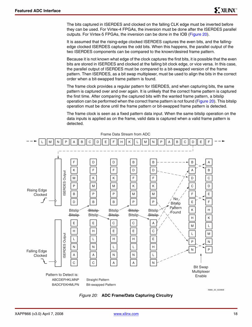
The bits captured in ISERDES and clocked on the falling CLK edge must be inverted before they can be used. For Virtex-4 FPGAs, the inversion must be done after the ISERDES parallel outputs. For Virtex-5 FPGAs, the inversion can be done in the IOB (Figure 20).
It is assumed that the rising-edge clocked ISERDES captures the even bits, and the falling-edge clocked ISERDES captures the odd bits. When this happens, the parallel output of the two ISERDES components can be compared to the known/desired frame pattern.
Because it is not known what edge of the clock captures the first bits, it is possible that the even bits are stored in ISERDES and clocked at the falling bit clock edge, or vice versa. In this case, the parallel output of ISERDES must be compared to a bit-swapped version of the frame pattern. Then ISERDES, as a bit swap multiplexer, must be used to align the bits in the correct order when a bit-swapped frame pattern is found.
The frame clock provides a regular pattern for ISERDES, and when capturing bits, the same pattern is captured over and over again. It is unlikely that the correct frame pattern is captured the first time. After comparing the captured bits with the wanted frame pattern, a bitslip operation can be performed when the correct frame pattern is not found (Figure 20). This bitslip operation must be done until the frame pattern or bit-swapped frame pattern is detected.
The frame clock is seen as a fixed pattern data input. When the same bitslip operation on the data inputs is applied as on the frame, valid data is captured when a valid frame pattern is detected.
X-Ref Target - Figure 20
Figure 20: ADC Frame/Data Capturing Circuitry
Frame Data Stream from ADC
Rising EdgeClocked
L M N P A B
F
K
M
P
B
D
D
F
K
M
P
B
D
F
K
M
P
B
B
D
F
K
M
P
B
D
F
K
M
P
B
A
D
C
F
E
A
B
C
D
E
F
C D E F H K L M N P A B C D E F
K
H
M
L
P
N
H
K
L
M
N
P
ISE
RD
ES
Out
put
Falling EdgeClocked
Pattern to Detect is:
BitslipBitslip
E
H
L
N
A
C
E
H
L
N
A
C
C
E
H
L
N
A
C
E
H
L
N
A
A
C
E
H
L
N
BitslipBitslip
BitslipBitslip
BitslipBitslip
Bitslip
NoBitslipPatternFound
Bit SwapMultiplexer
Enable
X866_20_022808
Bitslip
ABCDEFHKLMNP
BADCFEKHMLPN
Straight Pattern
Bit-swapped Pattern
ISE
RD
ES
Out
put

Featured ADC Interface
XAPP866 (v3.0) April 7, 2008 www.xilinx.com 19
R
Data
Data and frame capturing are identical except that no state machine is used in data capturing. The state machine aligned by the bitslip operation to the frame pattern is used at the same time in the data capturing circuit. Data and frame signals are phase aligned so that when a valid frame pattern is detected, the captured data is also valid.
The circuit used for data and frame capturing is shown in Figure 21. For frame captures, the elements displayed in blue are not used. For data captures, the elements displayed in red are not used.
The frame circuit design provides bitslip and multiplexer enable signals to each ADC data channel.
X-Ref Target - Figure 21
Figure 21: Bitslip Operation on the ADC Frame Clock
ISERDES
ISERDES
BITSLIP
X866_21_013008
BITSLIP
Frame PatternRecognition State
Machine
IBUFDS
DIFF_OUT
Clk
CLKDIV
ClkDiv
Bitslip_N_O
Bitslip_P_E
BitSwapMuxEna
FramePattern
BitSwappedFramePatternCLK
CLKDIV
CLK
OD
D1
3
5
7
1
3
5
7
0
2
4
6
O
Q1
Q2
Q3
Q4
Q5
Q6
Q1
Q2
Q3
Q4
Q5
Q6
ClkDiv
IBUFDS
DIFF_OUT
Virtex-5 Device
Virtex-4 Device: YesVirtex-5 Device: No

One-Wire ADC interface
XAPP866 (v3.0) April 7, 2008 www.xilinx.com 20
R
One-Wire ADC interface
The ADC transmits the digital bits over one differential LVDS channel. The number of transmitter bits is equal to the resolution of the ADC. In some ADC modes, the bits are packed in byte or word boundaries. For example, the Texas Instruments ADS6445 14-bit ADC used in one-wire, DDR, 16x serialization mode transmits the 14 bits in a word (16-bit) boundary. The unused bits are stuffed with 0s. This makes it easy to interface ADCs with 14-bit and 16-bit resolutions.
The ISERDES data and frame interface blocks cannot receive 16 bits at one time, but they can easily receive byte-wide frames and data. With some extra registers in the back of the interface, it is possible to receive 16-bit data. Figure 22 shows the block diagram of a single-channel, one-wire, 14-bit, DDR, 16x serialization interface.
The frame clock is treated like data. The ADC bit clock is used to register the serial received bits from the ADC, and a divided version of this clock is used as the clock for all actions after deserialization of the data.
Figure 2, page 3 shows the data, frame, and clock waveforms from the ADC. In these waveforms, the frame clock is the bit clock divided by 8 and then aligned to the data channels. When a BUFR divides the bit clock (DCLK) by 4, ISERDES receives 8 bits, which then are transferred to the parallel output of ISERDES. This way it is possible to receive two consecutive bytes and concatenate them in a register after ISERDES.
The frame pattern to search for is half an ADC frame pattern in this case. When half a frame pattern (11111111) is detected, the MSB of an ADC word is correctly received. The next byte is then the LSB of the 16-bit word transmitted by the ADC. Enabling two extra registers in a ping-pong structure from the CLKDIV clock allows both bytes to be easily concatenated. With the correct values set to the generic parameters in the HDL source code, the synthesis tool automatically generates the one-wire interface.
X-Ref Target - Figure 22
Figure 22: Single-Channel, One-Wire Interface
X866_22_013008
Reg
iste
r
Mul
tiple
xer
ISE
RD
ES
ISE
RD
ES
AdcDataChnlAdcClock
Data Out [15:0]
DA CLK
Com
para
tor
BitSwap Pattern
ISE
RD
ES
ISE
RD
ES
AdcFrame
FCLKPattern
FrameState
Machine
Done
Done
CLK
00000000
11111111
CLKDIV
Bitslip_N
Bitslip_P
SwapMuxEna
Com
para
tor
ISE
RD
ES
ClockState
Machine
IDELAY

Two-Wire ADC Interface
XAPP866 (v3.0) April 7, 2008 www.xilinx.com 21
R
Two-Wire ADC Interface
Because two data lanes are used per ADC, the following design blocks are needed for a one-channel ADC device:
• One clock adjustment module
• One frame pattern recognition module
• Two data capture blocks
Thus a four-channel device, such as the Texas Instruments ADS6445 ADC, needs eight data capturing blocks as shown in Figure 23.
The ADC transmits the result of a conversion over two differential lanes to the FPGA interface. Each lane carries half a conversion result of the ADC, as shown in Figure 3, page 3. By choosing this format, the frame, which remains a single-channel interface, carries an 8-bit pattern (11110000). When that pattern is correctly detected, all data channels receive correct data. The resulting output of the ISERDES components must then be arranged to finally produce a full ADC resolution result. The arrangement of the bits depends on the ADC transmission format chosen, i.e., MSB first then bit or byte mode. For example, a 14-bit ADC used in two-wire mode with 16x serialization and a DDR clock transmits byte data over two channels. The extra two bits are stuffed with 0s and are arranged in the byte pattern following the chosen transmission mode. Two data capturing modules deliver the data of one ADC channel. After capturing the data, the two channels must be assembled in a word with ADC resolution (Figure 24).
X-Ref Target - Figure 23
Figure 23: Two-Wire, Four-Channel ADC Interface
X866_23_013008
DA0[15:0]
DataOut [63:0]
[31:16]
[47:32]
[63:48]
DA1
FCLKAdcDataChnl
DB0
DB1
SwapMuxEnaBitslip_NBitslip_P
Done
AdcDataChnl
DC0
DC1
AdcDataChnl
DD0
DD1
AdcDataChnl
AdcFrame
DCLK
CLKCLKDIV
Done
AdcClock

PCB Design
XAPP866 (v3.0) April 7, 2008 www.xilinx.com 22
R
With the correct values are set to the generic parameters in the HDL source code, the synthesis tool automatically generates the two-wire interface.
PCB Design This section describes potential PCB layout issues.
Component Placement
Different circuit components should be placed as close as possible to each other on the PCB, aligned according to pinout. Components should be positioned to minimize the number of turns, corners, and vias. The flexibility of the FPGA pinout can assist in optimizing the PCB routing.
A straight, short connection improves all possible parameters of a PCB layout, namely:
• Signal integrity
• Transmission line effects
• Capacitance and inductance
• Operating frequency
Transmission line effects matter when distances between components are lengthy. All transmission lines should be terminated properly to control reflections.
Component Placement Examples
Virtex-4 and Virtex-5 devices have I/O arranged in banks. Although the size of the I/O bank is different for Virtex-4 and Virtex-5 devices, the same I/O placement rules can be applied to both FPGA families (Figure 25). For the classic ADC interface, the bit clock is routed onto a dedicated clock input, while the word (frame) clock uses a clock-capable I/O and data lines use normal I/O. For the featured ADC interface, clock-capable I/O should be used for the bit and word (frame) clocks, with the I/O for the data lines centered around these pins. In both cases, the pin arrangement proposed in Figure 25 can be used. These I/O locations should be set in the user constraints file (UCF). As a result, logic placement is controlled, and optimal FPGA timing is achieved. All LVDS transmission lines, data, clock, and frame should have the same length.
X-Ref Target - Figure 24
Figure 24: Interface Output Data Organization
12-bit14-bit16-bit
12-bit “0000” & [47:36] “0000” & [35:24] “0000” & [23:12] “0000” & [11:0]“00” & [55:42] “00” & [41:28] “00” & [27:14] “00” & [13:0]
63:48 47:32 31:16 15:014-bit16-bit
47:3655:4263:48
35:2441:2847:32
23:1227:1431:16
11:0Channel 4
ADCChnl 4
Output of the Data Interface
Data Out63:0 X866_24_013008
Output of the ADC Interface
Channel 3 Channel 2 Channel 1
Channel 4 Channel 3 Channel 2 Channel 1
13:015:0
ADCChnl 3
ADCChnl 2
ADCChnl 1

PCB Design
XAPP866 (v3.0) April 7, 2008 www.xilinx.com 23
R
Guidelines and Recommendations
The key guidelines for PCB designers are:
• Spend sufficient time when placing components for the layout.
• Keep trace lengths as short as possible.
• Spend time determining the number of PCB layers and how the layer stack-up is realized.
• If possible during PCB layout, keep the length of a track shorter than the travel and reflection time of the signal on the trace. If this is not possible, take transmission line theory into account.
• Match the length of all differential traces (data and clock).
• When making turns with differential traces, balance the number of left and right turns. When making a turn with a differential trace, the inner trace becomes shorter than the outer trace of the pair. When using more turns in one direction, one trace of the differential pair is longer than the other (without direct correction possibilities).
• Spread traces after routing over the available space of the PCB to minimize crosstalk.
• Do not route traces into 90° or 180° turns. Such turns increase the effective width of the trace, contributing to parasitic capacitance. At very fast edge rates, these discontinuities can cause significant signal integrity problems. Instead, use round, circular turns. If this is not possible, use 45° corners.
• Take the guidelines of the signal return paths into account.
• Guard traces.
• Remember the importance of ground planes.
• Specific to the TQFP package of the ADC device, use the thermal pad connection PowerPad to improve the operating stability of the device.
X-Ref Target - Figure 25
Figure 25: I/O Placement for Virtex-4 and Virtex-5 Devices
8 Pairs of Differential I/O 8 Pairs of Differential I/O
BUFIO
BUFR
IDELAYCTRL
7 Pairs of Differential I/O 7 Pairs of Differential I/O 7 Pairs of Differential I/O 7 Pairs of Differential I/O
X866_25_012008
Virtex-5 FPGA
Virtex-4 FPGA

Reference Designs
XAPP866 (v3.0) April 7, 2008 www.xilinx.com 24
R
Reference Designs
Table 2 provides the reference design matrix.
The README file included with the reference design files provides instructions on how to operate the reference design on a Texas Instruments TSW1200 demonstration board. To modify the generic HDL parameters in the source code, refer to Table 3 and Table 6, page 27.
Table 2: Reference Design Matrix
Parameter Description
General
Developer name Marc Defossez
Target Device Virtex-4 FPGA, Virtex-5 FPGA
Source code provided Yes
Source code format VHDL
Design uses code/IP from existing Xilinx application note/reference design, CORE Generator™ software or 3rd party
No
Simulation
Functional simulation performed Yes
Timing simulation performed On separate hierarchical levels
Testbench provided for functional/timing simulation For simulation separate hierarchical levels
Testbench format VHDL
Simulator software/version used ModelSim SE_6.2b
SPICE/IBIS simulations No
Implementation
Synthesis software tools/version used XST_9.2.04
Implementation software tools/version used ISE_9.2.04
Static timing analysis performed Yes
Hardware Verification
Hardware verified Yes
Hardware platform used for verification ML555 for Virtex-5 FPGAs and TSW1200 Texas Instruments demo board for Virtex-4 FPGAs

Reference Designs
XAPP866 (v3.0) April 7, 2008 www.xilinx.com 25
R
Guidelines for the Classic ADC Reference Design
The HDL code contains several generic parameters used to tailor the reference design to different ADC resolutions and channels (Table 3).
Design Specifics of the Classic ADC Reference Design
The parameters and specifications given in Table 4 are for the classic ADC interface implemented in a Virtex-4 XC4VLX25-11-FF363 FPGA. This device was used to verify and approve the reference design.
Table 3: Generic HDL Parameters for Classic ADC Reference Design Solution
Generic Parameter Description
C_FAMILY “virtex4” or “virtex5”
C_INTERFACE_LOC_XC_INTERFACE_LOC_Y
These two generics are equal to an RLOC_ORIGIN at the bottom-left corner of the interface design. The ADC interface fits an I/O bank; therefore, the logic must be locked with this restriction. For example, the Virtex-5 LX50T device has six I/O banks on the left as well as six clock regions. The logic in the regions starts at these locations:
I/O Bank Logic RAMB DSP
19 X0Y100 X0Y20 X0Y40
15 X0Y80 X0Y16 X0Y32
11 X0Y60 X0Y12 X0Y24
13 X0Y40 X0Y8 X0Y16
17 X0Y20 X0Y4 X0Y8
21 X0Y0 X0Y0 X0Y0
C_AdcChnls Number of channels in the ADC device. For Virtex-5 devices, one I/O bank can accept up to 8 channels. 1, 2, 4, and 8 channels are allowed for ADC resolutions of 12, 14, and 16 bits. Only 1, 2, or 4 channels are allowed for ADC with 24-bit resolution.
C_AdcBits ADC resolution: 12, 14, 16, or 24.
C_OnChipLvdsTerm Turns chip termination ON or OFF.
C_ExternalClockIn 1 = external clock is used and a DCM is added.
C_DataOutSel Selects the way the data is delivered to the application:000 = No registers or RAMB.001 = FF register set.010 = RAM used as register (fixed address).

Reference Designs
XAPP866 (v3.0) April 7, 2008 www.xilinx.com 26
R
Table 5 summarizes the classic ADC reference design utilization.
Table 4: Classic ADC Reference Design Specifics
Specification Number
Number of bits that can be captured with this interface 4–24
Maximum speed of the control, state machine, and design 200 MHz
Minimum bit-clock frequency DCM speed
Number of LVDS differential I/O pins required:
For bit clock 1 clock-capable pair
For frame clock 1 clock-capable pair
For 8 data lines (8 ADC channels in one-wire mode) 8 pairs
Number of other I/Os required:
SPI connection (RESET, PDN, SCLK, SDATA, and SEN) 5 LVCMOS
Number of ISERDES required: (ISERDES in IDDR mode)
For bit clock 0
For frame clock 1
For data per ADC in one-wire mode 8
For this interface 9
Table 5: Classic ACD Reference Design Utilization Summary
Component Percentage (%) Total Number Number Utilized
BUFIO 6 32 2
BUFR 8 24 2
IDELAYCTRL 6 16 1
LOCed IDELAYCTRL 100 1 1
ISERDES 4 448 19
Slice 1 10752 142
SLICEM 1 5376 11

Reference Designs
XAPP866 (v3.0) April 7, 2008 www.xilinx.com 27
R
Guidelines for the Featured ADC Reference Design
The HDL code contains several generic parameters used to tailor the featured ADC reference design to different ADC resolutions and channels (Table 6).
Design Specifics of the Featured ADC Reference Design
The parameters and specifications given in Table 7 are for the featured ADC interface implemented in a Virtex-4 XC4VLX25-11-FF363 FPGA. This device was used to verify and approve the reference design.
Table 6: Generic HDL Parameters for Featured ADC Reference Design Solution
Generic Parameter Description
C_FAMILY “virtex4” or “virtex5”
C_AdcChnls Number of channels in the ADC device. The design is developed for 1, 2, or 4 channels.
C_AdcBits ADC resolution: 12, 14, 16, or 24.
C_AdcMsbOrLsbFst 0 = LSB first, 1 = MSB first.
C_AdcBytOrBitMode 0 = Byte mode, 1 = Bit mode.
C_OnChipLvdsTerm 0 = no termination, 1 = termination.This parameter is only applicable to the IBUFDS input buffers in the source code. The IBUFDS_DIFF_OUT used buffers need to get the termination resistor setting in the UCF file.UCF example text: INST “NetName” DIFF_TERM = TRUE;
C_AdcWireInt 1 = One-wire interface2 = Two-wire interface
C_FrmPattern Frame pattern to discover. Any pattern can be supplied:• ADS6445 (14/16-bit)
♦ Two-wire pattern: 0000000011110000♦ One-wire pattern: 1111111100000000
• ADS6425♦ Two-wire pattern: 000000111000♦ One-wire pattern: 111111000000
C_StatTaps Default set to 31. Start position of the clock adjust IDELAY.
C_IdelayCtrlLoc Fixes the IdelayCtrl component in a particular place on the FPGA. Syntax: “IDELAYCTRL_XxYy” where x and y are the rows and columns.
C_FrameDcm Fixes the DCM. If used, this parameter distributes the adjusted frame clock in a particular place of the FPGA.Syntax: “DCM_ADV_XxYy” where x and y are the rows and columns.
Table 7: Featured ADC Reference Design Specifics
Specification Number
Number of bits that can be captured with this interface 4–24
Maximum speed of the control, state machine, and design 200 MHz
Minimum bit-clock frequency 220–240 MHz
Number of LVDS differential I/O pins required:
For bit clock 1 clock-capable pair
For frame clock 1 clock-capable pair

Reference Designs
XAPP866 (v3.0) April 7, 2008 www.xilinx.com 28
R
Table 8 summarizes the featured ADC reference design utilization.
Design Setup
The reference design files are available for download from:
https://secure.xilinx.com/webreg/clickthrough.do?cid=55677
This ZIP file contains:
• Ads527x_V4_V5: Classical implementation of a one-wire interface. Originally developed for ADS527x ADC devices. [Ref 1]
• Ads6000_V4_1w_NoBramNoProc: A one-wire implementation of an ADS6xxx interface for a Virtex-4 device.
• Ads6000_V4_2w_NoBramNoProc: A two-wire implementation of an ADS6xxx interface for a Virtex-4 device.
• Ads_Usb_To_Uart: A sample design to connect the ADC SPI port via a UART_2_USB device to a PC. This design uses a PicoBlaze processor core.
Both one-wire and two-wire implementations are identical. The two-wire design is preset for two-wire applications, and the one-wire design is preset for one-wire applications.
For 8 data lines (4 ADC channels in two-wire mode) 8 pairs
Number of other I/Os required:
SPI connection (RESET, PDN, SCLK, SDATA, and SEN) 5 LVCMOS
Number of ISERDES required:
For bit clock 1 or 2
For frame clock 2
For data per ADC in two-wire mode 4
For this interface 16
Number of RAMB18 required (if option enabled) At least one
Table 8: Featured ADC Reference Design Utilization Summary
Component Percentage (%) Total Number Number Utilized
BUFIO 6 32 2
BUFR 8 24 2
IDELAYCTRL 6 16 1
LOCed IDELAYCTRL 100 1 1
ISERDES 4 448 19
Slice 1 10752 142
SLICEM 1 5376 11
Table 7: Featured ADC Reference Design Specifics (Cont’d)
Specification Number

Conclusion
XAPP866 (v3.0) April 7, 2008 www.xilinx.com 29
R
The design directories are set up as shown in Figure 26.
Conclusion Virtex-4 and Virtex-5 FPGAs provide flexible and versatile platforms for building interfaces to all the latest ADC families from Texas Instruments. The interfaces either use specific Virtex-4 or Virtex-5 FPGA features or can be built out of generic logic. In addition, interfaces can be constructed to be compatible with older ADC families and provide an upgrade path for existing and new designs. It is also possible to use the techniques described in this application note and the accompanying reference designs for higher speed and/or higher resolution ADCs.
X-Ref Target - Figure 26
Figure 26: Design Directory Setup
Implementation of the Design
Simulation .do Compile FilesSimulation Work DirectorySynthesis DirectoryOne Subdirectory per used Synthesis ToolProject and other User Constraint FilesSource Code
Top-level .vhd Implementation
Top-level Testbench and Top-level Tester
All hierarchical levels have their own subdirectory and are treated by the synthesis tool as libraries
X866_26_012108

References
XAPP866 (v3.0) April 7, 2008 www.xilinx.com 30
R
References 1. XAPP774, Connecting Xilinx FPGAs to Texas Instruments ADS527x Series ADCs.
2. UG070, Virtex-4 User Guide.
3. UG190, Virtex-5 FPGA User Guide.
4. Texas Instruments ADC data sheets are available for download at:http://focus.ti.com/paramsearch/docs/parametricsearch.tsp?family=analog&familyId=390&uiTemplateId=NODE_STRY_PGE_T
Additional Resources
1. DS302, Virtex-4 Data Sheet: DC and Switching Characteristics.
2. UG072, Virtex-4 PCB Designer’s Guide.
3. DS202, Virtex-5 Data Sheet: DC and Switching Characteristics.
4. UG195, Virtex-5 Packaging and Pinout Specification.
5. UG203, Virtex-5 PCB Designer’s Guide.
Revision History
The following table shows the revision history for this document:
Notice of Disclaimer
Xilinx is disclosing this Application Note to you “AS-IS” with no warranty of any kind. This Application Noteis one possible implementation of this feature, application, or standard, and is subject to change withoutfurther notice from Xilinx. You are responsible for obtaining any rights you may require in connection withyour use or implementation of this Application Note. XILINX MAKES NO REPRESENTATIONS ORWARRANTIES, WHETHER EXPRESS OR IMPLIED, STATUTORY OR OTHERWISE, INCLUDING,WITHOUT LIMITATION, IMPLIED WARRANTIES OF MERCHANTABILITY, NONINFRINGEMENT, ORFITNESS FOR A PARTICULAR PURPOSE. IN NO EVENT WILL XILINX BE LIABLE FOR ANY LOSS OFDATA, LOST PROFITS, OR FOR ANY SPECIAL, INCIDENTAL, CONSEQUENTIAL, OR INDIRECTDAMAGES ARISING FROM YOUR USE OF THIS APPLICATION NOTE.
Date Version Description of Revisions
04/13/07 1.0 Initial Xilinx release.
07/10/07 2.0 Complete rewrite. This version applies the design methodology discussed in XAPP774 to Virtex-4 and Virtex-5 devices to enable the design of one-wire and two-wire ADC interfaces.
08/13/07 2.0.1 Minor typographical edit.
04/07/08 3.0 Major update for ADC with serial LVDS interface.