Embed Size (px)
Citation preview
XAPP1002 (v1.0) October 22, 2007 www.xilinx.com 1
© 2007 Xilinx, Inc. All rights reserved. XILINX, the Xilinx logo, and other designated brands included herein are trademarks of Xilinx, Inc. All other trademarks are the property of their respective owners. PCI, PCI-SIG, PCI EXPRESS, PCIE, PCI-X, PCI HOT PLUG, MINI PCI, EXPRESSMODULE, and the PCI, PCI-X, PCI HOT PLUG, and MINI PC design marks are trademarks, registered trademarks, and/or service marks of PCI-SIG.
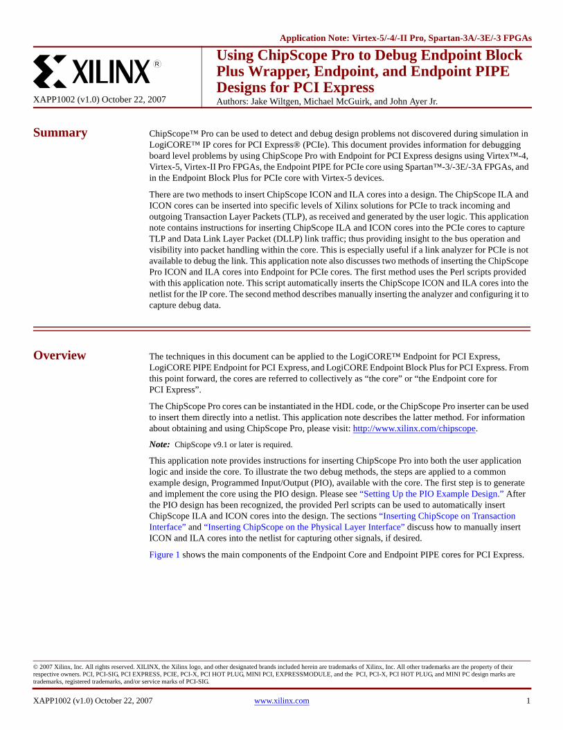
Summary ChipScope™ Pro can be used to detect and debug design problems not discovered during simulation in LogiCORE™ IP cores for PCI Express® (PCIe). This document provides information for debugging board level problems by using ChipScope Pro with Endpoint for PCI Express designs using Virtex™-4, Virtex-5, Virtex-II Pro FPGAs, the Endpoint PIPE for PCIe core using Spartan™-3/-3E/-3A FPGAs, and in the Endpoint Block Plus for PCIe core with Virtex-5 devices.
There are two methods to insert ChipScope ICON and ILA cores into a design. The ChipScope ILA and ICON cores can be inserted into specific levels of Xilinx solutions for PCIe to track incoming and outgoing Transaction Layer Packets (TLP), as received and generated by the user logic. This application note contains instructions for inserting ChipScope ILA and ICON cores into the PCIe cores to capture TLP and Data Link Layer Packet (DLLP) link traffic; thus providing insight to the bus operation and visibility into packet handling within the core. This is especially useful if a link analyzer for PCIe is not available to debug the link. This application note also discusses two methods of inserting the ChipScope Pro ICON and ILA cores into Endpoint for PCIe cores. The first method uses the Perl scripts provided with this application note. This script automatically inserts the ChipScope ICON and ILA cores into the netlist for the IP core. The second method describes manually inserting the analyzer and configuring it to capture debug data.
Overview The techniques in this document can be applied to the LogiCORE™ Endpoint for PCI Express, LogiCORE PIPE Endpoint for PCI Express, and LogiCORE Endpoint Block Plus for PCI Express. From this point forward, the cores are referred to collectively as “the core” or “the Endpoint core for PCI Express”.
The ChipScope Pro cores can be instantiated in the HDL code, or the ChipScope Pro inserter can be used to insert them directly into a netlist. This application note describes the latter method. For information about obtaining and using ChipScope Pro, please visit: http://www.xilinx.com/chipscope.
Note: ChipScope v9.1 or later is required.
This application note provides instructions for inserting ChipScope Pro into both the user application logic and inside the core. To illustrate the two debug methods, the steps are applied to a common example design, Programmed Input/Output (PIO), available with the core. The first step is to generate and implement the core using the PIO design. Please see “Setting Up the PIO Example Design.” After the PIO design has been recognized, the provided Perl scripts can be used to automatically insert ChipScope ILA and ICON cores into the design. The sections “Inserting ChipScope on Transaction Interface” and “Inserting ChipScope on the Physical Layer Interface” discuss how to manually insert ICON and ILA cores into the netlist for capturing other signals, if desired.
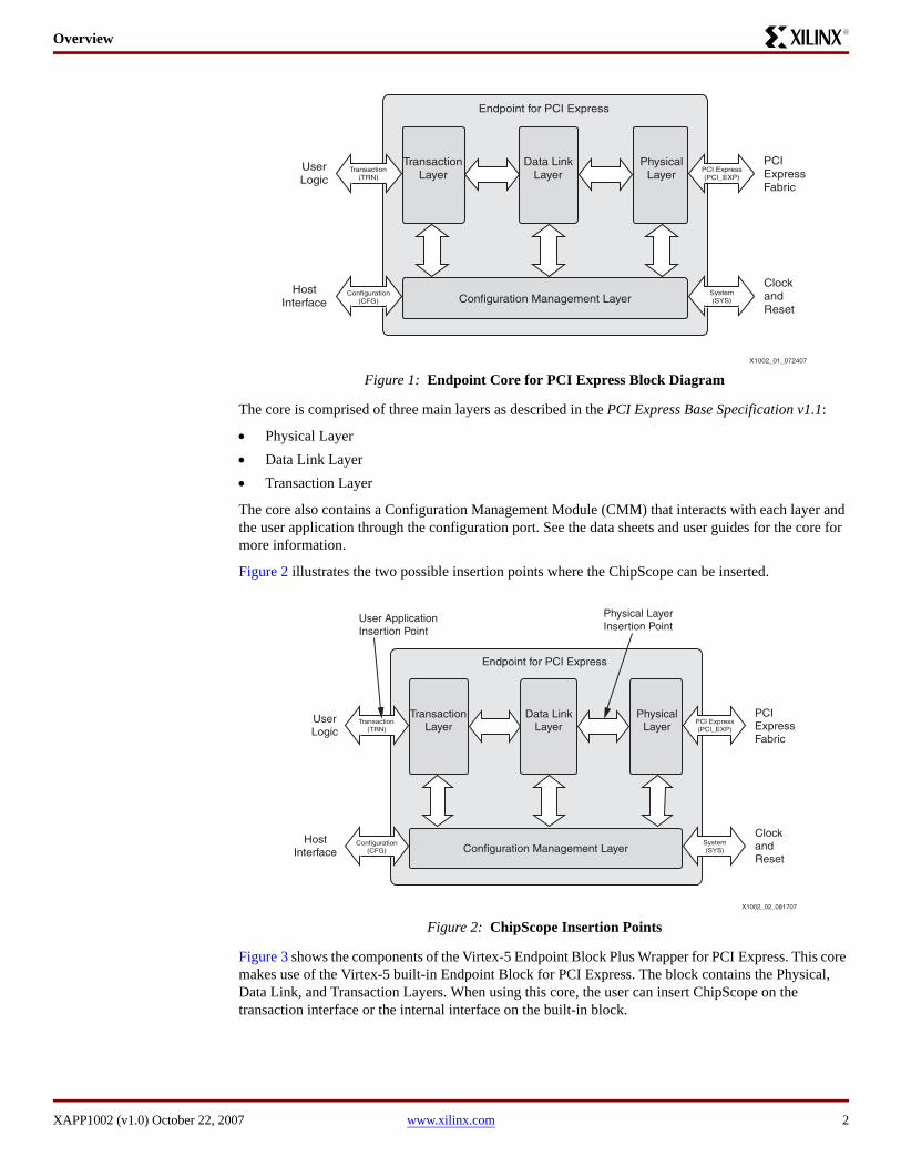
Figure 1 shows the main components of the Endpoint Core and Endpoint PIPE cores for PCI Express.
Application Note: Virtex-5/-4/-II Pro, Spartan-3A/-3E/-3 FPGAs
XAPP1002 (v1.0) October 22, 2007
Using ChipScope Pro to Debug Endpoint Block Plus Wrapper, Endpoint, and Endpoint PIPE Designs for PCI ExpressAuthors: Jake Wiltgen, Michael McGuirk, and John Ayer Jr.
R
Overview
XAPP1002 (v1.0) October 22, 2007 www.xilinx.com 2
R
The core is comprised of three main layers as described in the PCI Express Base Specification v1.1:
• Physical Layer• Data Link Layer• Transaction Layer
The core also contains a Configuration Management Module (CMM) that interacts with each layer and the user application through the configuration port. See the data sheets and user guides for the core for more information.
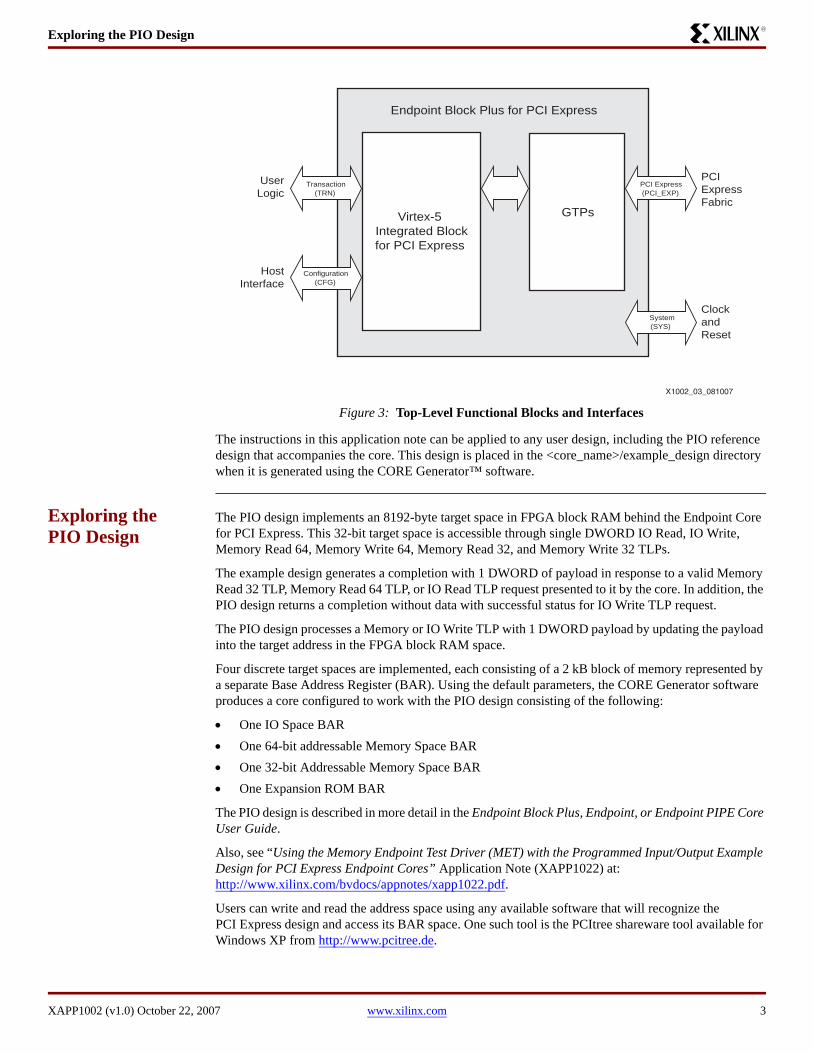
Figure 2 illustrates the two possible insertion points where the ChipScope can be inserted.
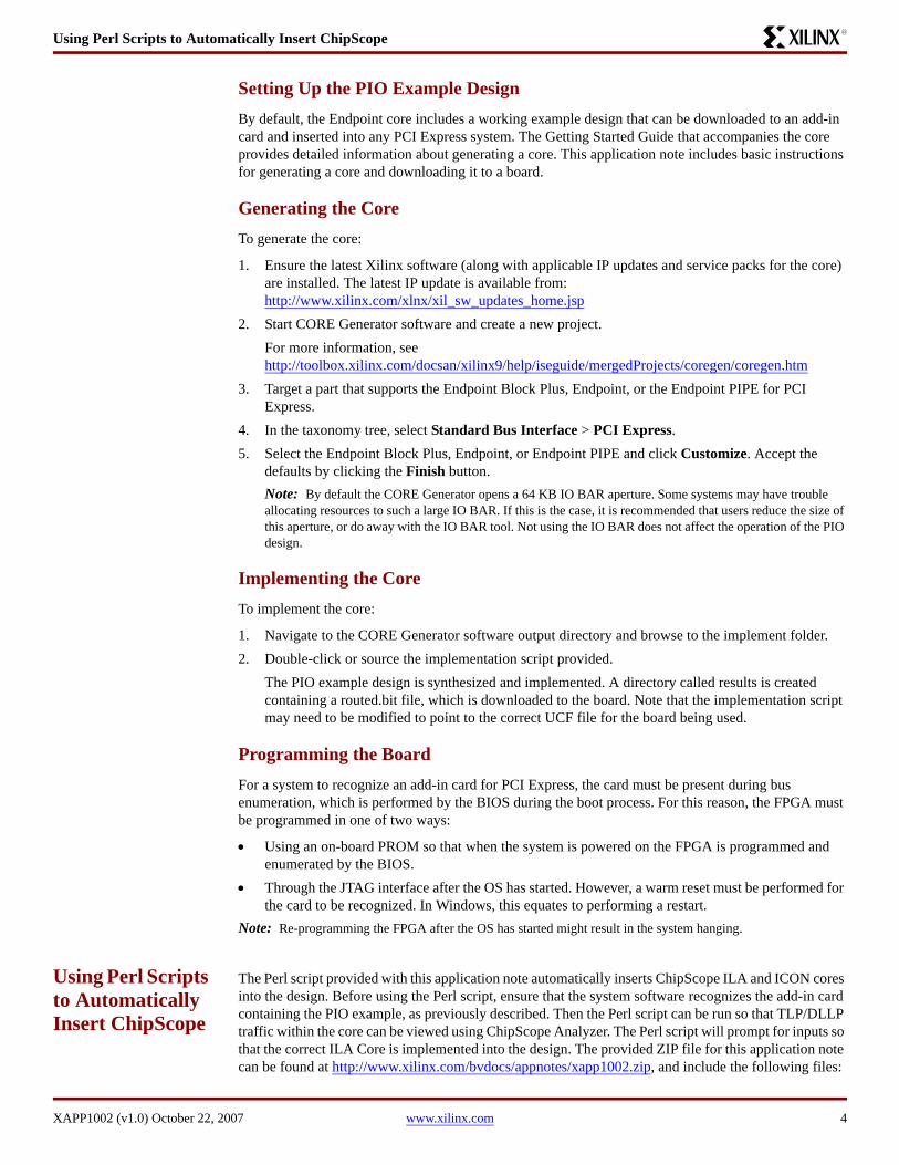
Figure 3 shows the components of the Virtex-5 Endpoint Block Plus Wrapper for PCI Express. This core makes use of the Virtex-5 built-in Endpoint Block for PCI Express. The block contains the Physical, Data Link, and Transaction Layers. When using this core, the user can insert ChipScope on the transaction interface or the internal interface on the built-in block.
Figure 1: Endpoint Core for PCI Express Block Diagram
Figure 2: ChipScope Insertion Points
UserLogic
HostInterface
PCI ExpressFabric
Endpoint for PCI Express
PhysicalLayer
Data LinkLayer
TransactionLayer
Configuration Management LayerClockandReset
Transaction(TRN)
Configuration(CFG)
PCI Express(PCI_EXP)
System(SYS)
X1002_01_072407
UserLogic
HostInterface
PCI ExpressFabric
Endpoint for PCI Express
PhysicalLayer
Data LinkLayer
TransactionLayer
Configuration Management LayerClockandReset
Transaction(TRN)
Configuration(CFG)
PCI Express(PCI_EXP)
System(SYS)
Physical LayerInsertion Point
User ApplicationInsertion Point
X1002_02_081707
Exploring the PIO Design
XAPP1002 (v1.0) October 22, 2007 www.xilinx.com 3
R
The instructions in this application note can be applied to any user design, including the PIO reference design that accompanies the core. This design is placed in the <core_name>/example_design directory when it is generated using the CORE Generator™ software.
Exploring the PIO Design
The PIO design implements an 8192-byte target space in FPGA block RAM behind the Endpoint Core for PCI Express. This 32-bit target space is accessible through single DWORD IO Read, IO Write, Memory Read 64, Memory Write 64, Memory Read 32, and Memory Write 32 TLPs.
The example design generates a completion with 1 DWORD of payload in response to a valid Memory Read 32 TLP, Memory Read 64 TLP, or IO Read TLP request presented to it by the core. In addition, the PIO design returns a completion without data with successful status for IO Write TLP request.
The PIO design processes a Memory or IO Write TLP with 1 DWORD payload by updating the payload into the target address in the FPGA block RAM space.
Four discrete target spaces are implemented, each consisting of a 2 kB block of memory represented by a separate Base Address Register (BAR). Using the default parameters, the CORE Generator software produces a core configured to work with the PIO design consisting of the following:
• One IO Space BAR• One 64-bit addressable Memory Space BAR• One 32-bit Addressable Memory Space BAR• One Expansion ROM BAR
The PIO design is described in more detail in the Endpoint Block Plus, Endpoint, or Endpoint PIPE Core User Guide.
Also, see “Using the Memory Endpoint Test Driver (MET) with the Programmed Input/Output Example Design for PCI Express Endpoint Cores” Application Note (XAPP1022) at: http://www.xilinx.com/bvdocs/appnotes/xapp1022.pdf.
Users can write and read the address space using any available software that will recognize the PCI Express design and access its BAR space. One such tool is the PCItree shareware tool available for Windows XP from http://www.pcitree.de.
Figure 3: Top-Level Functional Blocks and Interfaces
Virtex-5 Integrated Blockfor PCI Express
GTPs
Endpoint Block Plus for PCI Express
PCI Express(PCI_EXP)
System(SYS)
Transaction(TRN)
Configuration(CFG)
PCI ExpressFabric
UserLogic
HostInterface
Clockand Reset
X1002_03_081007
Using Perl Scripts to Automatically Insert ChipScope
XAPP1002 (v1.0) October 22, 2007 www.xilinx.com 4
R
Setting Up the PIO Example DesignBy default, the Endpoint core includes a working example design that can be downloaded to an add-in card and inserted into any PCI Express system. The Getting Started Guide that accompanies the core provides detailed information about generating a core. This application note includes basic instructions for generating a core and downloading it to a board.
Generating the CoreTo generate the core:
1. Ensure the latest Xilinx software (along with applicable IP updates and service packs for the core) are installed. The latest IP update is available from: http://www.xilinx.com/xlnx/xil_sw_updates_home.jsp
2. Start CORE Generator software and create a new project.For more information, see http://toolbox.xilinx.com/docsan/xilinx9/help/iseguide/mergedProjects/coregen/coregen.htm
3. Target a part that supports the Endpoint Block Plus, Endpoint, or the Endpoint PIPE for PCI Express.
4. In the taxonomy tree, select Standard Bus Interface > PCI Express.5. Select the Endpoint Block Plus, Endpoint, or Endpoint PIPE and click Customize. Accept the
defaults by clicking the Finish button.Note: By default the CORE Generator opens a 64 KB IO BAR aperture. Some systems may have trouble allocating resources to such a large IO BAR. If this is the case, it is recommended that users reduce the size of this aperture, or do away with the IO BAR tool. Not using the IO BAR does not affect the operation of the PIO design.
Implementing the CoreTo implement the core:
1. Navigate to the CORE Generator software output directory and browse to the implement folder.2. Double-click or source the implementation script provided.
The PIO example design is synthesized and implemented. A directory called results is created containing a routed.bit file, which is downloaded to the board. Note that the implementation script may need to be modified to point to the correct UCF file for the board being used.
Programming the BoardFor a system to recognize an add-in card for PCI Express, the card must be present during bus enumeration, which is performed by the BIOS during the boot process. For this reason, the FPGA must be programmed in one of two ways:
• Using an on-board PROM so that when the system is powered on the FPGA is programmed and enumerated by the BIOS.
• Through the JTAG interface after the OS has started. However, a warm reset must be performed for the card to be recognized. In Windows, this equates to performing a restart.
Note: Re-programming the FPGA after the OS has started might result in the system hanging.
Using Perl Scripts to Automatically Insert ChipScope
The Perl script provided with this application note automatically inserts ChipScope ILA and ICON cores into the design. Before using the Perl script, ensure that the system software recognizes the add-in card containing the PIO example, as previously described. Then the Perl script can be run so that TLP/DLLP traffic within the core can be viewed using ChipScope Analyzer. The Perl script will prompt for inputs so that the correct ILA Core is implemented into the design. The provided ZIP file for this application note can be found at http://www.xilinx.com/bvdocs/appnotes/xapp1002.zip, and include the following files:
Using Perl Scripts to Automatically Insert ChipScope
XAPP1002 (v1.0) October 22, 2007 www.xilinx.com 5
R
• insert_chipscope.pl - Perl script fileThis file creates the ChipScope Inserter project file and inserts the ILA and ICON cores into the design netlist.
• *.cdc - ChipScope project fileThis file contains project-specific information and is taken in by ChipScope Inserter.
When extracting the ZIP file, please be sure to extract it to the same level as the core netlist. This location is typically the top level of the core output hierarchy. A CDC directory is added at this level and contains core-specific CDC file that should be used when running the script.
Running the ScriptThe Perl script can be invoked by using the xilperl tool provided with Xilinx ISE™ design tools.
1. At the command prompt, navigate to the directory where you have placed the script.2. Type xilperl insert_chipscope.pl
The script will run and prompt you for information as needed.3. After entering the required information, the script places the ChipScope ICON and ILA cores into
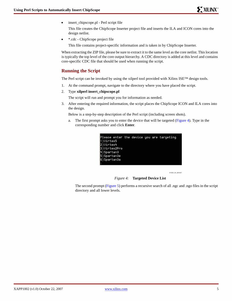
the design.Below is a step-by-step description of the Perl script (including screen shots).a. The first prompt asks you to enter the device that will be targeted (Figure 4). Type in the
corresponding number and click Enter.
The second prompt (Figure 5) performs a recursive search of all .ngc and .ngo files in the script directory and all lower levels.
X-Ref Target - Figure 4
Figure 4: Targeted Device ListX1002_04_081007
Using Perl Scripts to Automatically Insert ChipScope
XAPP1002 (v1.0) October 22, 2007 www.xilinx.com 6
R
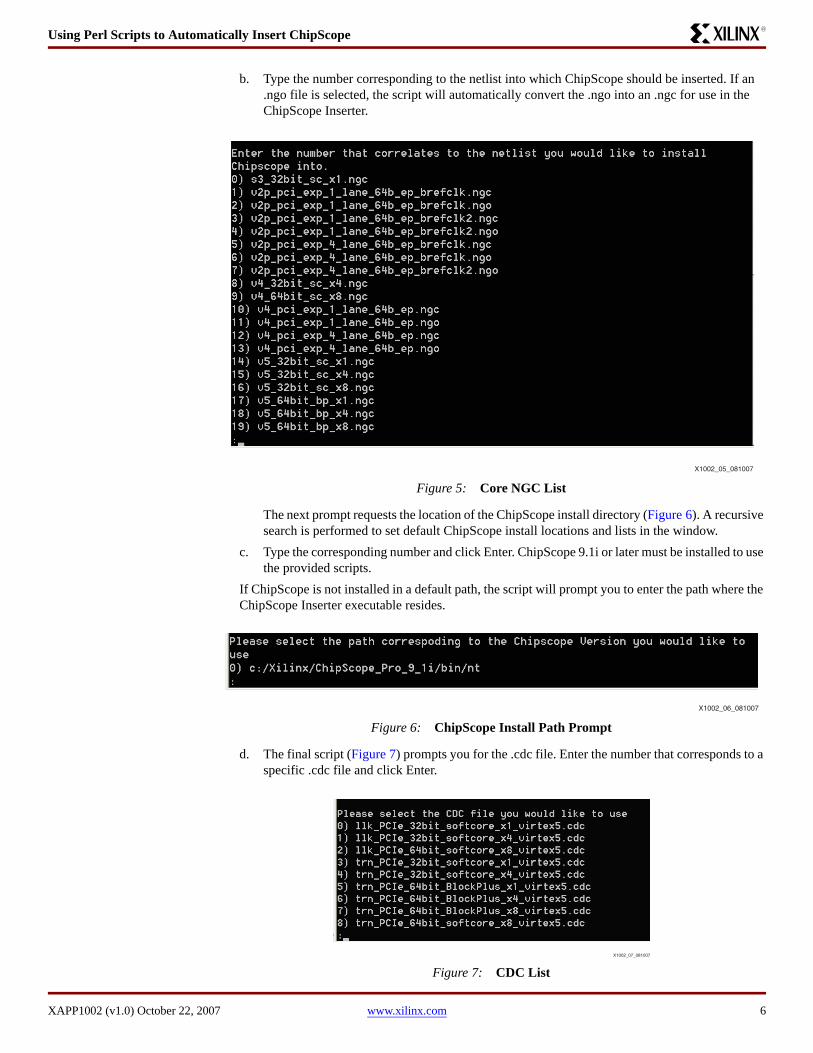
b. Type the number corresponding to the netlist into which ChipScope should be inserted. If an .ngo file is selected, the script will automatically convert the .ngo into an .ngc for use in the ChipScope Inserter.
The next prompt requests the location of the ChipScope install directory (Figure 6). A recursive search is performed to set default ChipScope install locations and lists in the window.
c. Type the corresponding number and click Enter. ChipScope 9.1i or later must be installed to use the provided scripts.
If ChipScope is not installed in a default path, the script will prompt you to enter the path where the ChipScope Inserter executable resides.
d. The final script (Figure 7) prompts you for the .cdc file. Enter the number that corresponds to a specific .cdc file and click Enter.
X-Ref Target - Figure 5
Figure 5: Core NGC List
X-Ref Target - Figure 6
Figure 6: ChipScope Install Path Prompt
X-Ref Target - Figure 7
Figure 7: CDC List
X1002_05_081007
X1002_06_081007
X1002_07_081007
Using Perl Scripts to Automatically Insert ChipScope
XAPP1002 (v1.0) October 22, 2007 www.xilinx.com 7
R
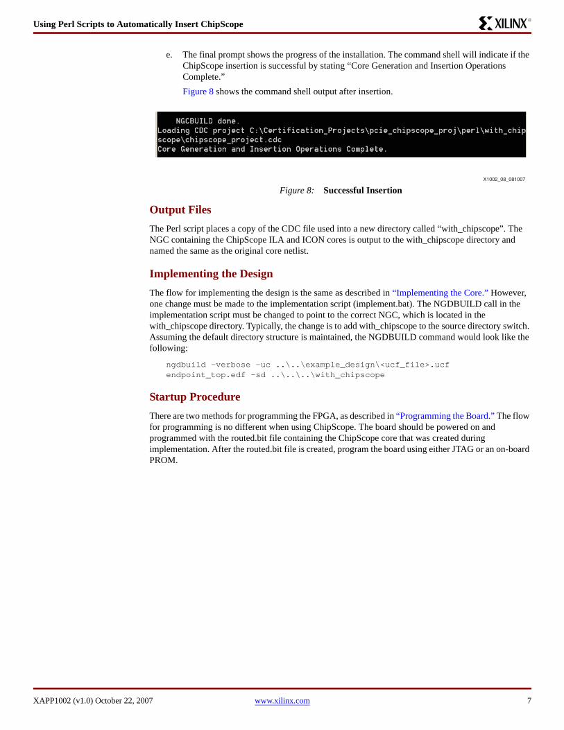
e. The final prompt shows the progress of the installation. The command shell will indicate if the ChipScope insertion is successful by stating “Core Generation and Insertion Operations Complete.”Figure 8 shows the command shell output after insertion.
Output FilesThe Perl script places a copy of the CDC file used into a new directory called “with_chipscope”. The NGC containing the ChipScope ILA and ICON cores is output to the with_chipscope directory and named the same as the original core netlist.
Implementing the DesignThe flow for implementing the design is the same as described in “Implementing the Core.” However, one change must be made to the implementation script (implement.bat). The NGDBUILD call in the implementation script must be changed to point to the correct NGC, which is located in the with_chipscope directory. Typically, the change is to add with_chipscope to the source directory switch. Assuming the default directory structure is maintained, the NGDBUILD command would look like the following:
ngdbuild -verbose -uc ..\..\example_design\<ucf_file>.ucf endpoint_top.edf -sd ..\..\..\with_chipscope
Startup ProcedureThere are two methods for programming the FPGA, as described in “Programming the Board.” The flow for programming is no different when using ChipScope. The board should be powered on and programmed with the routed.bit file containing the ChipScope core that was created during implementation. After the routed.bit file is created, program the board using either JTAG or an on-board PROM.
X-Ref Target - Figure 8
Figure 8: Successful InsertionX1002_08_081007
Using Perl Scripts to Automatically Insert ChipScope
XAPP1002 (v1.0) October 22, 2007 www.xilinx.com 8
R
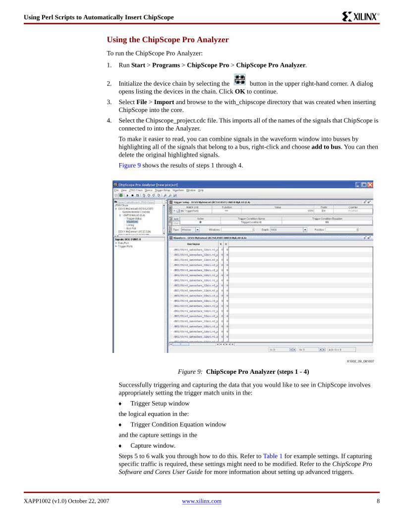
Using the ChipScope Pro AnalyzerTo run the ChipScope Pro Analyzer:
1. Run Start > Programs > ChipScope Pro > ChipScope Pro Analyzer.
2. Initialize the device chain by selecting the button in the upper right-hand corner. A dialog opens listing the devices in the chain. Click OK to continue.
3. Select File > Import and browse to the with_chipscope directory that was created when inserting ChipScope into the core.
4. Select the Chipscope_project.cdc file. This imports all of the names of the signals that ChipScope is connected to into the Analyzer. To make it easier to read, you can combine signals in the waveform window into busses by highlighting all of the signals that belong to a bus, right-click and choose add to bus. You can then delete the original highlighted signals.Figure 9 shows the results of steps 1 through 4.
Successfully triggering and capturing the data that you would like to see in ChipScope involves appropriately setting the trigger match units in the:♦ Trigger Setup windowthe logical equation in the:♦ Trigger Condition Equation windowand the capture settings in the ♦ Capture window.Steps 5 to 6 walk you through how to do this. Refer to Table 1 for example settings. If capturing specific traffic is required, these settings might need to be modified. Refer to the ChipScope Pro Software and Cores User Guide for more information about setting up advanced triggers.
Figure 9: ChipScope Pro Analyzer (steps 1 - 4)
X1002_09_081007
Using Perl Scripts to Automatically Insert ChipScope
XAPP1002 (v1.0) October 22, 2007 www.xilinx.com 9
R
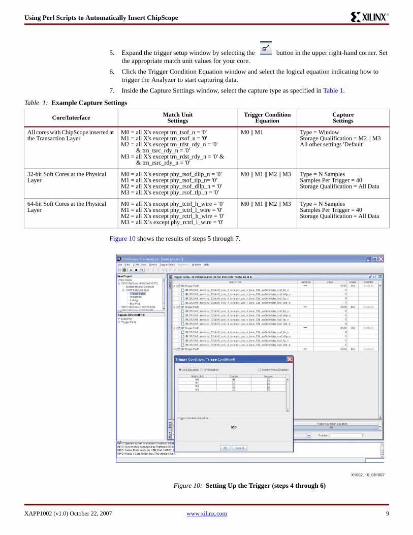
5. Expand the trigger setup window by selecting the button in the upper right-hand corner. Set the appropriate match unit values for your core.
6. Click the Trigger Condition Equation window and select the logical equation indicating how to trigger the Analyzer to start capturing data.
7. Inside the Capture Settings window, select the capture type as specified in Table 1.
Figure 10 shows the results of steps 5 through 7.
Table 1: Example Capture Settings
Core/Interface Match Unit Settings
Trigger Condition Equation
Capture Settings
All cores with ChipScope inserted at the Transaction Layer
M0 = all X's except trn_tsof_n = '0'M1 = all X's except trn_rsof_n = '0'M2 = all X's except trn_tdst_rdy_n = '0' & trn_tsrc_rdy_n = '0'M3 = all X's except trn_rdst_rdy_n = '0' & & trn_rsrc_rdy_n = '0'
M0 || M1 Type = WindowStorage Qualification = M2 || M3 All other settings 'Default'
32-bit Soft Cores at the Physical Layer
M0 = all X's except phy_tsof_dllp_n = '0'M1 = all X's except phy_tsof_tlp_n= '0'M2 = all X's except phy_rsof_dllp_n = '0'M3 = all X's except phy_rsof_tlp_n = '0'
M0 || M1 || M2 || M3 Type = N SamplesSamples Per Trigger = 40Storage Qualification = All Data
64-bit Soft Cores at the Physical Layer
M0 = all X's except phy_tctrl_h_wire = '0'M1 = all X's except phy_tctrl_l_wire = '0'M2 = all X's except phy_rctrl_h_wire = '0'M3 = all X’s except phy_rctrl_l_wire = '0'
M0 || M1 || M2 || M3 Type = N SamplesSamples Per Trigger = 40Storage Qualification = All Data
Figure 10: Setting Up the Trigger (steps 4 through 6)
X1002_10_081007
Manual ChipScope Insertion
XAPP1002 (v1.0) October 22, 2007 www.xilinx.com 10
R
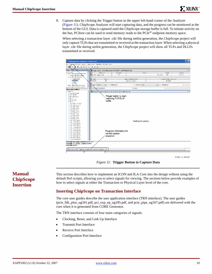
8. Capture data by clicking the Trigger button in the upper left-hand corner of the Analyzer (Figure 11). ChipScope Analyzer will start capturing data, and the progress can be monitored at the bottom of the GUI. Data is captured until the ChipScope storage buffer is full. To initiate activity on the bus, PCItree can be used to send memory reads to the PCIe® endpoint memory space.When selecting a transaction layer .cdc file during netlist generation, the ChipScope project will only capture TLPs that are transmitted or received at the transaction layer. When selecting a physical layer .cdc file during netlist generation, the ChipScope project will show all TLPs and DLLPs transmitted or received.
Manual ChipScope Insertion
This section describes how to implement an ICON and ILA Core into the design without using the default Perl scripts, allowing you to select signals for viewing. The sections below provide examples of how to select signals at either the Transaction or Physical Layer level of the core.
Inserting ChipScope on Transaction InterfaceThe core user guides describe the user application interface (TRN interface). The user guides (pcie_blk_plus_ug341.pdf, pci_exp_ep_ug185.pdf, and pcie_pipe_ug167.pdf) are delivered with the core when it is generated from CORE Generator.
The TRN interface consists of four main categories of signals:
• Clocking, Reset, and Link Up Interface• Transmit Port Interface• Receive Port Interface• Configuration Port Interface
Figure 11: Trigger Button to Capture DataX1002_11_081007
Manual ChipScope Insertion
XAPP1002 (v1.0) October 22, 2007 www.xilinx.com 11
R
The signals viewed in ChipScope depend on the problem being addressed. In this example, the primary signals on the transmit and receive interface, along with status signals from the configuration interface, are viewed. This allows for the capture of incoming and outgoing TLPs, along with error status signals to identify any error conditions the endpoint encounters. To capture data, trigger signals are also added to ChipScope. The exact triggers used are dependent on the scenario and the desired information.
The main signals that indicate the beginning and ending TLPs, along with suggested triggers, are shown in Table 2 and Table 3. When using ChipScope to capture data off of the TRN interface, the clock signal used for ChipScope should be the trn_clk output from the core (Table 4).
Table 2: TRN Interface Signals
Name Direction Description
trn_lnk_up_n Output Transaction Link Up: Active low - Transaction link-up is asserted when the core and the connected upstream link partner port are ready and able to exchange data packetsTransaction link-up is de-asserted when the core and link partner are attempting to establish communication, and when communication with the link partner is lost due to errors on the transmission channel. When the core is driven to Hot Reset and Link Disable states by the link partner, trn_lnk_up_n is de-asserted and all TLPs stored in the endpoint core are lost
User Application Transmit Interface
trn_tsof_n Input Active low - Signals the start of a packet
trn_teof_n Input Active low - Signals the end of a packet
trn_td[n:0] Input Packet data to be transmitted. “n” is dependent upon specific core used
trn_tdst_rdy_n Output Active low - Indicates the core is ready to accept data on trn_td. The simultaneous assertion of trn_tsrc_rdy_n and trn_tdst_rdy_n marks a successful transfer
trn_tsrc_rdy_n Input Active low- Indicates user application is presenting valid data on trn_td
trn_tbuf_av[n:0] Output Endpoint for PCI Express: Number of transmit buffers available in the core. Each buffer holds one max size TLP. “n” is dependent upon the specific core usedEndpoint Block Plus for PCI Express: Indicates if at least one free buffer exists in the Posted, Non-Posted, or Completion transmit buffers
User Application Receive Interface
trn_rsof_n Output Active low - Signals the start of a packet
trn_reof_n Output Active low - Signals the end of a packet
trn_rd[n:0] Output Packet data to be received. “n” is dependent upon specific core used
trn_rdst_rdy_n Input Active low - Indicates the user application is ready to accept data on trn_rd. The simultaneous assertion of trn_rdst_rdy_n and trn_rsrc_rdy_n marks a successful transfer
trn_rsrc_rdy_n Output Active low - Indicates the core is presenting valid data on trn_rd
Manual ChipScope Insertion
XAPP1002 (v1.0) October 22, 2007 www.xilinx.com 12
R
trn_rbar_hit[6:0] Output Active low - Indicates BAR(s) targeted by the current receive transactiontrn_rbar_hit_n[0] => BAR1trn_rbar_hit_n[1] => BAR2trn_rbar_hit_n[2] => BAR3trn_rbar_hit_n[3] => BAR4trn_rbar_hit_n[4] => BAR5trn_rbar_hit_n[5] => BAR6trn_rbar_hit_n[6] => Expansion ROM AddressNote that if two BARs are configured into single 64-bit address, both corresponding trn_rbar_hit_n bits are asserted
User Application Configuration Interface
cfg_dstatus[3:0] Output The device status register from the PCI Express Extended Capability Structure
cfg_dcommand[3:0] Output The device control register from the PCI Express Extended Capability Structure
Table 3: ChipScope Trigger Signals
Name Description
trn_tsof_n Trigger - On start of any TLP transferred from User Application to PCIe® Endpoint
trn_rsof_n Trigger - On start of any TLP transferred from PCIe Endpoint to User Application
trn_teof_n Trigger - On end of any TLP transferred from User Application to PCIe Endpoint
trn_reof_n Trigger - On end of any TLP transferred from PCIe Endpoint to User Application
trn_tsrc_rdy_n Storage Qualification - Capture when packet is being transmitted from User Application to Endpoint
trn_rsrc_rdy_n Storage Qualification - Capture when User Application is receiving packet from PCIe Endpoint
Table 4: ChipScope Clock Signal
Name Description
trn_clk Transaction layer clock to clock ChipScope ICON and ILA cores
Table 2: TRN Interface Signals (Cont’d)
Name Direction Description
Manual ChipScope Insertion
XAPP1002 (v1.0) October 22, 2007 www.xilinx.com 13
R
Inserting ChipScope on the Physical Layer InterfaceThe transaction interface does not show TLPs or DLLPs that are consumed by the core. Designers using the Endpoint or Endpoint PIPE for PCI Express cores can insert ChipScope between the Physical and Data Link layers to grab internal core signals to capture these packets. The core consumes configuration read and write (CfgRd, CfgWr) TLPs, all message TLPs (except vendor defined messages), and any malformed TLP. All DLLP traffic is consumed by the core.
For debug purposes, it is often helpful to view these packets and capture the internal transmit, and receive paths allow you to see all TLP and DLLP traffic. Tables 5 through 8 show examples of signals that can be captured at the Physical Layer interface to monitor all incoming TLP and DLLP traffic. As with capturing data on the Transaction Layer Interface, the same trn_clk is used to sample data on the Physical Layer interface. This interface is operating on the same trn_clk domain and frequency. Depending on the core being used, the data path width is either 32-bits or 64-bits wide.
Designs using the Virtex-5 Endpoint Block Plus Wrapper for PCI Express cannot view TLPs or DLLPs consumed by the built-in Endpoint Block. All DLLP traffic and TLP traffic, such as configuration TLPs and malformed TLPs, are consumed by the block.
Table 5: 32-bit Data Path Physical Layer Interface
Name Description
trn_lnk_up_n Transaction Link Up: Active low - Transaction link-up is asserted when the core and the connected upstream link partner port are ready and able to exchange data packets
Internal Transmit Data Path
phy_tsof_dllp_n Active low - Signals the start of a DLLP packet
phy_tsof_tlp_n Active low - Signals the start of a TLP packet
phy_teof_n Active low - Signals the end of a TLP or DLLP packet
phy_td[31:0] Packet data to be received
Internal Receive Data Path
phy_rsof_dllp_n Active low - Signals the start of a DLLP packet
phy_rsof_dllp_n Active low - Signals the start of a TLP packet
phy_reof_n Active low - Signals the end of a TLP or DLLP packet
phy_rd[31:0] Packet data to be received
Table 6: 32-bit Data Path Physical Layer Trigger Signals
Name Description
phy_tsof_dllp_n Trigger - On start of any DLLP transferred on the internal transmit bus
phy_tsof_tlp_n Trigger - On start of any TLP transferred on the internal transmit bus
phy_rsof_dllp_n Trigger - On end of any DLLP transferred on the internal receive bus
phy_rsof_tlp_n Trigger - On end of any TLP transferred on the internal receive bus
Manual ChipScope Insertion
XAPP1002 (v1.0) October 22, 2007 www.xilinx.com 14
R
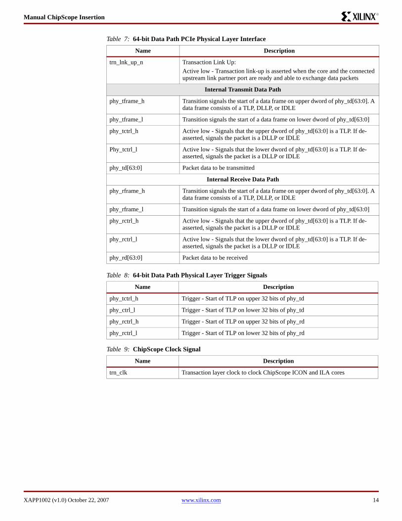
Table 7: 64-bit Data Path PCIe Physical Layer Interface
Name Description
trn_lnk_up_n Transaction Link Up: Active low - Transaction link-up is asserted when the core and the connected upstream link partner port are ready and able to exchange data packets
Internal Transmit Data Path
phy_tframe_h Transition signals the start of a data frame on upper dword of phy_td[63:0]. A data frame consists of a TLP, DLLP, or IDLE
phy_tframe_l Transition signals the start of a data frame on lower dword of phy_td[63:0]
phy_tctrl_h Active low - Signals that the upper dword of phy_td[63:0] is a TLP. If de-asserted, signals the packet is a DLLP or IDLE
Phy_tctrl_l Active low - Signals that the lower dword of phy_td[63:0] is a TLP. If de-asserted, signals the packet is a DLLP or IDLE
phy_td[63:0] Packet data to be transmitted
Internal Receive Data Path
phy_rframe_h Transition signals the start of a data frame on upper dword of phy_td[63:0]. A data frame consists of a TLP, DLLP, or IDLE
phy_rframe_l Transition signals the start of a data frame on lower dword of phy_td[63:0]
phy_rctrl_h Active low - Signals that the upper dword of phy_td[63:0] is a TLP. If de-asserted, signals the packet is a DLLP or IDLE
phy_rctrl_l Active low - Signals that the lower dword of phy_td[63:0] is a TLP. If de-asserted, signals the packet is a DLLP or IDLE
phy_rd[63:0] Packet data to be received
Table 8: 64-bit Data Path Physical Layer Trigger Signals
Name Description
phy_tctrl_h Trigger - Start of TLP on upper 32 bits of phy_td
phy_ctrl_l Trigger - Start of TLP on lower 32 bits of phy_td
phy_rctrl_h Trigger - Start of TLP on upper 32 bits of phy_rd
phy_rctrl_l Trigger - Start of TLP on lower 32 bits of phy_rd
Table 9: ChipScope Clock Signal
Name Description
trn_clk Transaction layer clock to clock ChipScope ICON and ILA cores
Manual ChipScope Insertion
XAPP1002 (v1.0) October 22, 2007 www.xilinx.com 15
R
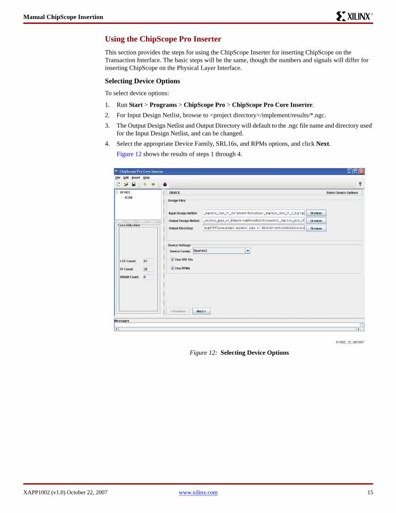
Using the ChipScope Pro InserterThis section provides the steps for using the ChipScope Inserter for inserting ChipScope on the Transaction Interface. The basic steps will be the same, though the numbers and signals will differ for inserting ChipScope on the Physical Layer Interface.
Selecting Device Options
To select device options:
1. Run Start > Programs > ChipScope Pro > ChipScope Pro Core Inserter.2. For Input Design Netlist, browse to <project directory>/implement/results/*.ngc.3. The Output Design Netlist and Output Directory will default to the .ngc file name and directory used
for the Input Design Netlist, and can be changed.4. Select the appropriate Device Family, SRL16s, and RPMs options, and click Next.
Figure 12 shows the results of steps 1 through 4.
Figure 12: Selecting Device Options
X1002_12_081007
Manual ChipScope Insertion
XAPP1002 (v1.0) October 22, 2007 www.xilinx.com 16
R
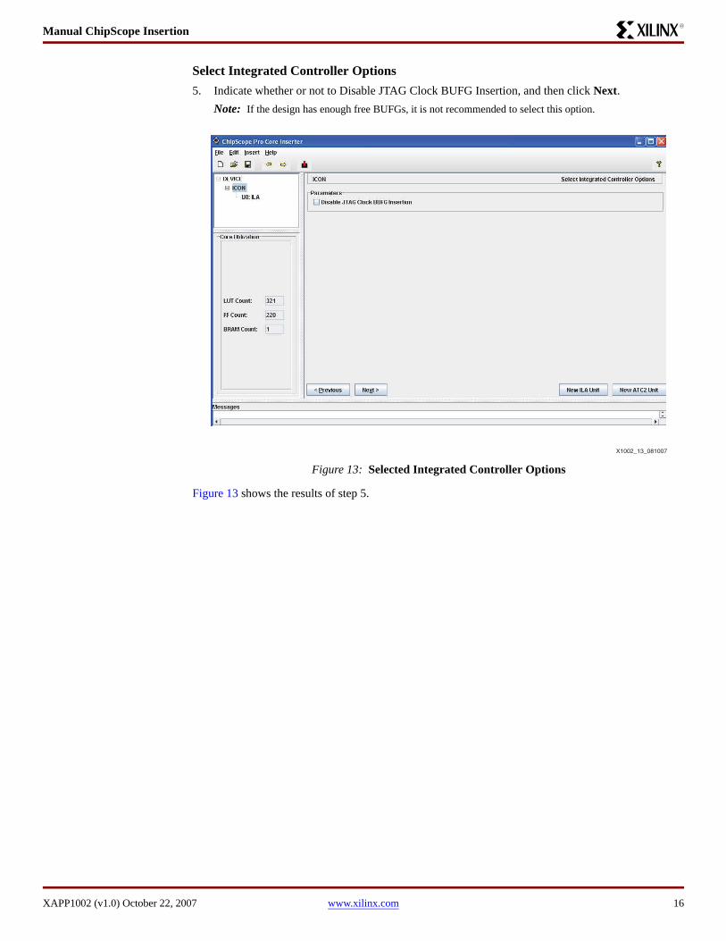
Select Integrated Controller Options5. Indicate whether or not to Disable JTAG Clock BUFG Insertion, and then click Next.
Note: If the design has enough free BUFGs, it is not recommended to select this option.
Figure 13 shows the results of step 5.
Figure 13: Selected Integrated Controller Options
X1002_13_081007
Manual ChipScope Insertion
XAPP1002 (v1.0) October 22, 2007 www.xilinx.com 17
R
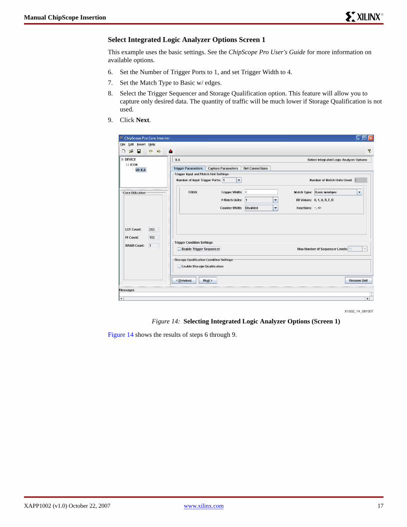
Select Integrated Logic Analyzer Options Screen 1
This example uses the basic settings. See the ChipScope Pro User's Guide for more information on available options.
6. Set the Number of Trigger Ports to 1, and set Trigger Width to 4.7. Set the Match Type to Basic w/ edges.8. Select the Trigger Sequencer and Storage Qualification option. This feature will allow you to
capture only desired data. The quantity of traffic will be much lower if Storage Qualification is not used.
9. Click Next.
Figure 14 shows the results of steps 6 through 9.
Figure 14: Selecting Integrated Logic Analyzer Options (Screen 1)
X1002_14_081007
Manual ChipScope Insertion
XAPP1002 (v1.0) October 22, 2007 www.xilinx.com 18
R
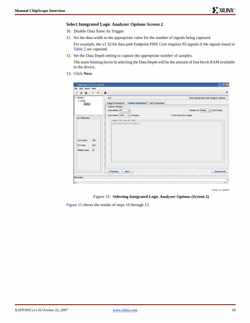
Select Integrated Logic Analyzer Options Screen 210. Disable Data Same As Trigger.11. Set the data width to the appropriate value for the number of signals being captured.
For example, the x1 32-bit data path Endpoint PIPE Core requires 93 signals if the signals listed in Table 2 are captured.
12. Set the Data Depth setting to capture the appropriate number of samples. The main limiting factor in selecting the Data Depth will be the amount of free block RAM available in the device.
13. Click Next.
Figure 15 shows the results of steps 10 through 13.
Figure 15: Selecting Integrated Logic Analyzer Options (Screen 2)
X1002_15_081007
Manual ChipScope Insertion
XAPP1002 (v1.0) October 22, 2007 www.xilinx.com 19
R
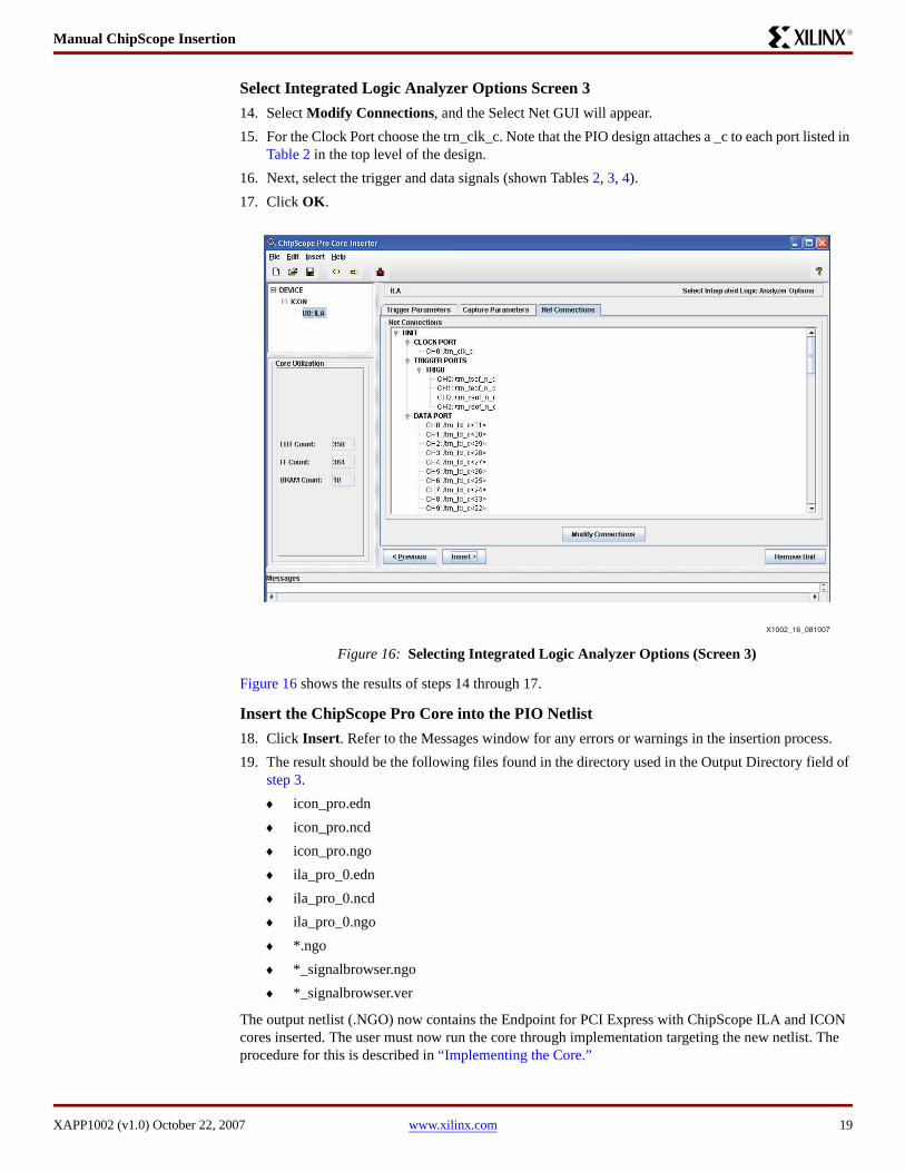
Select Integrated Logic Analyzer Options Screen 314. Select Modify Connections, and the Select Net GUI will appear.15. For the Clock Port choose the trn_clk_c. Note that the PIO design attaches a _c to each port listed in
Table 2 in the top level of the design.16. Next, select the trigger and data signals (shown Tables 2, 3, 4).17. Click OK.
Figure 16 shows the results of steps 14 through 17.
Insert the ChipScope Pro Core into the PIO Netlist18. Click Insert. Refer to the Messages window for any errors or warnings in the insertion process. 19. The result should be the following files found in the directory used in the Output Directory field of
step 3.♦ icon_pro.edn♦ icon_pro.ncd♦ icon_pro.ngo♦ ila_pro_0.edn♦ ila_pro_0.ncd♦ ila_pro_0.ngo♦ *.ngo♦ *_signalbrowser.ngo♦ *_signalbrowser.ver
The output netlist (.NGO) now contains the Endpoint for PCI Express with ChipScope ILA and ICON cores inserted. The user must now run the core through implementation targeting the new netlist. The procedure for this is described in “Implementing the Core.”
Figure 16: Selecting Integrated Logic Analyzer Options (Screen 3)
X1002_16_081007
Interpreting ChipScope Output
XAPP1002 (v1.0) October 22, 2007 www.xilinx.com 20
R
Interpreting ChipScope Output
This section describes how to properly decode and identify the incoming packets at both the transaction layer and physical layer interfaces.
Transaction Layer OutputA valid TLP starts on a trn_tsof_n or trn_rsof_n assertion. The trn_td or trn_rd bus contains valid packet header and data between the assertion of trn_tsof_n/trn_rsof_n and trn_teof_n/trn_reof_n. A valid transfer between the user application occurs only when the core and the user application are ready to transfer data. The core and user application indicate this using trn_tsrc_rdy_n and trn_rsrc_rdy_n for transmitting packets and trn_tdst_rdy_n and trn_rdst_rdy_n for receiving packets. The packet is transferred or received synchronous to the rising edge of trn_clk. The transaction layer interface is thoroughly described in the core user guide.
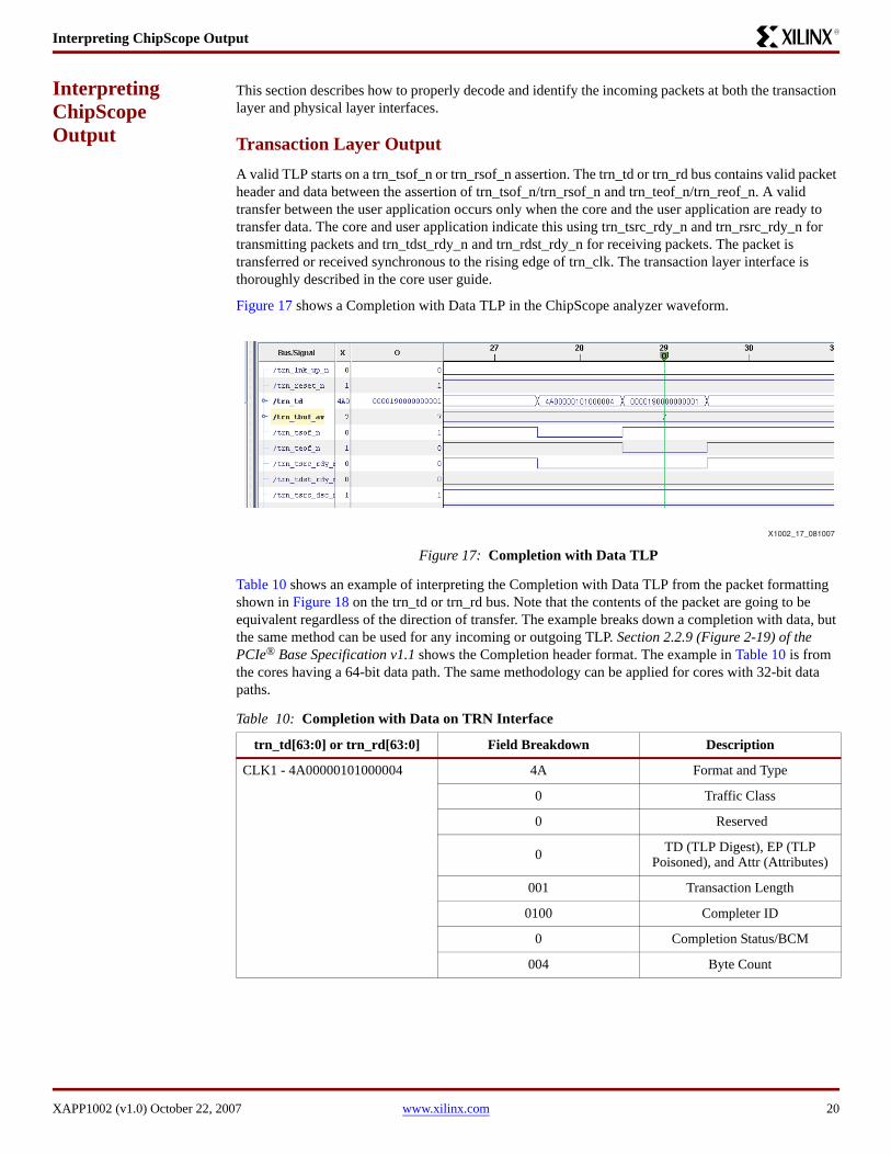
Figure 17 shows a Completion with Data TLP in the ChipScope analyzer waveform.
Table 10 shows an example of interpreting the Completion with Data TLP from the packet formatting shown in Figure 18 on the trn_td or trn_rd bus. Note that the contents of the packet are going to be equivalent regardless of the direction of transfer. The example breaks down a completion with data, but the same method can be used for any incoming or outgoing TLP. Section 2.2.9 (Figure 2-19) of the PCIe® Base Specification v1.1 shows the Completion header format. The example in Table 10 is from the cores having a 64-bit data path. The same methodology can be applied for cores with 32-bit data paths.
Figure 17: Completion with Data TLP
Table 10: Completion with Data on TRN Interface
trn_td[63:0] or trn_rd[63:0] Field Breakdown Description
CLK1 - 4A00000101000004 4A Format and Type
0 Traffic Class
0 Reserved
0 TD (TLP Digest), EP (TLP Poisoned), and Attr (Attributes)
001 Transaction Length
0100 Completer ID
0 Completion Status/BCM
004 Byte Count
X1002_17_081007
Interpreting ChipScope Output
XAPP1002 (v1.0) October 22, 2007 www.xilinx.com 21
R
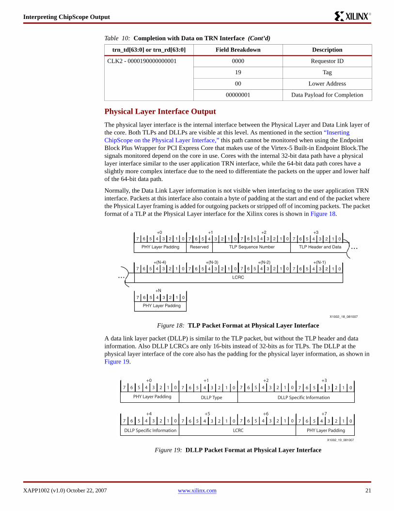
Physical Layer Interface OutputThe physical layer interface is the internal interface between the Physical Layer and Data Link layer of the core. Both TLPs and DLLPs are visible at this level. As mentioned in the section “Inserting ChipScope on the Physical Layer Interface,” this path cannot be monitored when using the Endpoint Block Plus Wrapper for PCI Express Core that makes use of the Virtex-5 Built-in Endpoint Block.The signals monitored depend on the core in use. Cores with the internal 32-bit data path have a physical layer interface similar to the user application TRN interface, while the 64-bit data path cores have a slightly more complex interface due to the need to differentiate the packets on the upper and lower half of the 64-bit data path.
Normally, the Data Link Layer information is not visible when interfacing to the user application TRN interface. Packets at this interface also contain a byte of padding at the start and end of the packet where the Physical Layer framing is added for outgoing packets or stripped off of incoming packets. The packet format of a TLP at the Physical Layer interface for the Xilinx cores is shown in Figure 18.
A data link layer packet (DLLP) is similar to the TLP packet, but without the TLP header and data information. Also DLLP LCRCs are only 16-bits instead of 32-bits as for TLPs. The DLLP at the physical layer interface of the core also has the padding for the physical layer information, as shown in Figure 19.
CLK2 - 0000190000000001 0000 Requestor ID
19 Tag
00 Lower Address
00000001 Data Payload for Completion
Figure 18: TLP Packet Format at Physical Layer Interface
Figure 19: DLLP Packet Format at Physical Layer Interface
Table 10: Completion with Data on TRN Interface (Cont’d)
trn_td[63:0] or trn_rd[63:0] Field Breakdown Description
X1002_18_081007
PHY Layer Padding TLP Sequence Number TLP Header and DataReserved
LCRC
7 6 5 4 3 2 1 0 7 6 5 4 3 2 1 0 7 6 5 4 3 2 1 0 7 6 5 4 3 2 1 0
+0 +1 +2 +3
PHY Layer Padding
7 6 5 4 3 2 1 0
+N
7 6 5 4 3 2 1 0 7 6 5 4 3 2 1 0 7 6 5 4 3 2 1 0 7 6 5 4 3 2 1 0
+(N-4) +(N-3) +(N-2) +(N-1)
...
...
X1002_19_081007
PHY Layer Padding DLLP Specific InformationDLLP Type
LCRC
7 6 5 4 3 2 1 0 7 6 5 4 3 2 1 0 7 6 5 4 3 2 1 0 7 6 5 4 3 2 1 0
+0 +1 +2 +3
PHY Layer Padding
7 6 5 4 3 2 1 0 7 6 5 4 3 2 1 0 7 6 5 4 3 2 1 0 7 6 5 4 3 2 1 0
+4 +5 +6 +7
DLLP Specific Information
Interpreting ChipScope Output
XAPP1002 (v1.0) October 22, 2007 www.xilinx.com 22
R
Cores with 32-bit Data Paths
A valid TLP starts on a phy_tsof_tlp_n or phy_rsof_tlp_n assertion and ends on a phy_teof_tlp_n or phy_reof_tlp_n assertion. Similar to the user application TRN interface, data is synchronous to the rising edge of the clock and is valid from the assertion of the start-of-frame signal until the assertion of the end-of-frame signal.
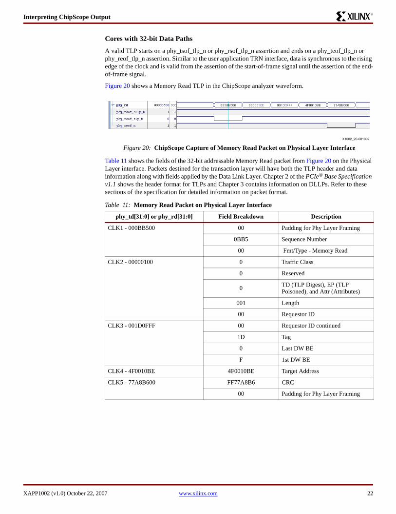
Figure 20 shows a Memory Read TLP in the ChipScope analyzer waveform.
Table 11 shows the fields of the 32-bit addressable Memory Read packet from Figure 20 on the Physical Layer interface. Packets destined for the transaction layer will have both the TLP header and data information along with fields applied by the Data Link Layer. Chapter 2 of the PCIe® Base Specification v1.1 shows the header format for TLPs and Chapter 3 contains information on DLLPs. Refer to these sections of the specification for detailed information on packet format.
Figure 20: ChipScope Capture of Memory Read Packet on Physical Layer Interface
Table 11: Memory Read Packet on Physical Layer Interface
phy_td[31:0] or phy_rd[31:0] Field Breakdown Description
CLK1 - 000BB500 00 Padding for Phy Layer Framing
0BB5 Sequence Number
00 Fmt/Type - Memory Read
CLK2 - 00000100 0 Traffic Class
0 Reserved
0 TD (TLP Digest), EP (TLP Poisoned), and Attr (Attributes)
001 Length
00 Requestor ID
CLK3 - 001D0FFF 00 Requestor ID continued
1D Tag
0 Last DW BE
F 1st DW BE
CLK4 - 4F0010BE 4F0010BE Target Address
CLK5 - 77A8B600 FF77A8B6 CRC
00 Padding for Phy Layer Framing
X1002_20-081007
Interpreting ChipScope Output
XAPP1002 (v1.0) October 22, 2007 www.xilinx.com 23
R
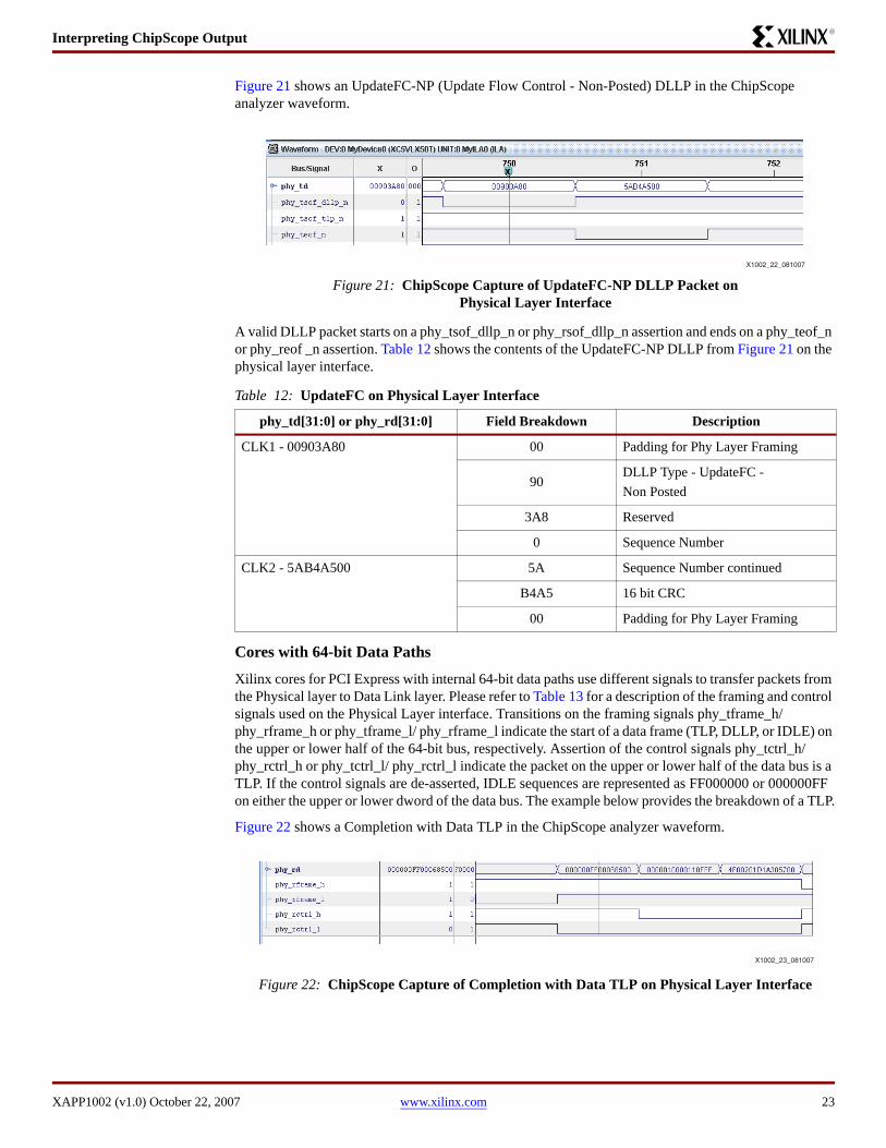
Figure 21 shows an UpdateFC-NP (Update Flow Control - Non-Posted) DLLP in the ChipScope analyzer waveform.
A valid DLLP packet starts on a phy_tsof_dllp_n or phy_rsof_dllp_n assertion and ends on a phy_teof_n or phy_reof _n assertion. Table 12 shows the contents of the UpdateFC-NP DLLP from Figure 21 on the physical layer interface.
Cores with 64-bit Data Paths
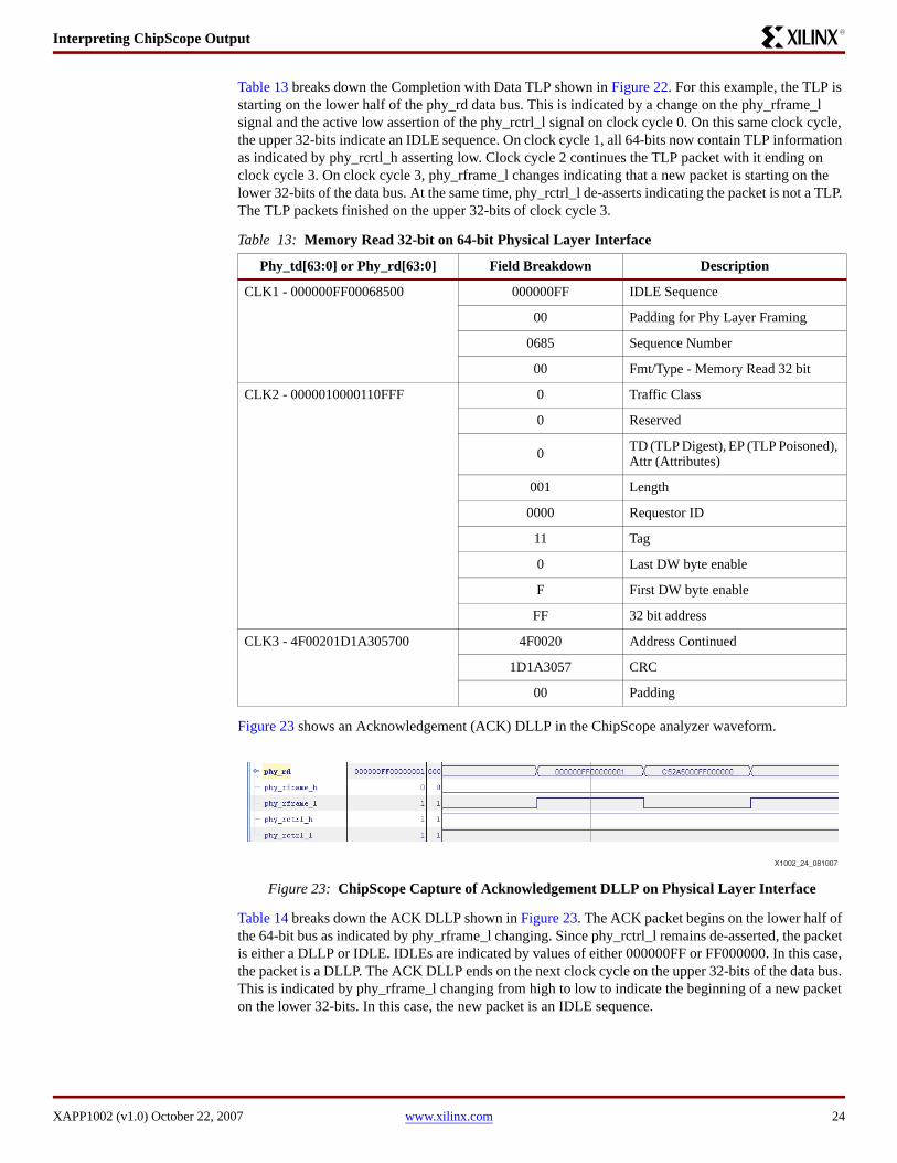
Xilinx cores for PCI Express with internal 64-bit data paths use different signals to transfer packets from the Physical layer to Data Link layer. Please refer to Table 13 for a description of the framing and control signals used on the Physical Layer interface. Transitions on the framing signals phy_tframe_h/ phy_rframe_h or phy_tframe_l/ phy_rframe_l indicate the start of a data frame (TLP, DLLP, or IDLE) on the upper or lower half of the 64-bit bus, respectively. Assertion of the control signals phy_tctrl_h/ phy_rctrl_h or phy_tctrl_l/ phy_rctrl_l indicate the packet on the upper or lower half of the data bus is a TLP. If the control signals are de-asserted, IDLE sequences are represented as FF000000 or 000000FF on either the upper or lower dword of the data bus. The example below provides the breakdown of a TLP.
Figure 22 shows a Completion with Data TLP in the ChipScope analyzer waveform.
Figure 21: ChipScope Capture of UpdateFC-NP DLLP Packet on Physical Layer Interface
Table 12: UpdateFC on Physical Layer Interface
phy_td[31:0] or phy_rd[31:0] Field Breakdown Description
CLK1 - 00903A80 00 Padding for Phy Layer Framing
90DLLP Type - UpdateFC - Non Posted
3A8 Reserved
0 Sequence Number
CLK2 - 5AB4A500 5A Sequence Number continued
B4A5 16 bit CRC
00 Padding for Phy Layer Framing
Figure 22: ChipScope Capture of Completion with Data TLP on Physical Layer Interface
X1002_22_081007
X1002_23_081007
Interpreting ChipScope Output
XAPP1002 (v1.0) October 22, 2007 www.xilinx.com 24
R
Table 13 breaks down the Completion with Data TLP shown in Figure 22. For this example, the TLP is starting on the lower half of the phy_rd data bus. This is indicated by a change on the phy_rframe_l signal and the active low assertion of the phy_rctrl_l signal on clock cycle 0. On this same clock cycle, the upper 32-bits indicate an IDLE sequence. On clock cycle 1, all 64-bits now contain TLP information as indicated by phy_rcrtl_h asserting low. Clock cycle 2 continues the TLP packet with it ending on clock cycle 3. On clock cycle 3, phy_rframe_l changes indicating that a new packet is starting on the lower 32-bits of the data bus. At the same time, phy_rctrl_l de-asserts indicating the packet is not a TLP. The TLP packets finished on the upper 32-bits of clock cycle 3.
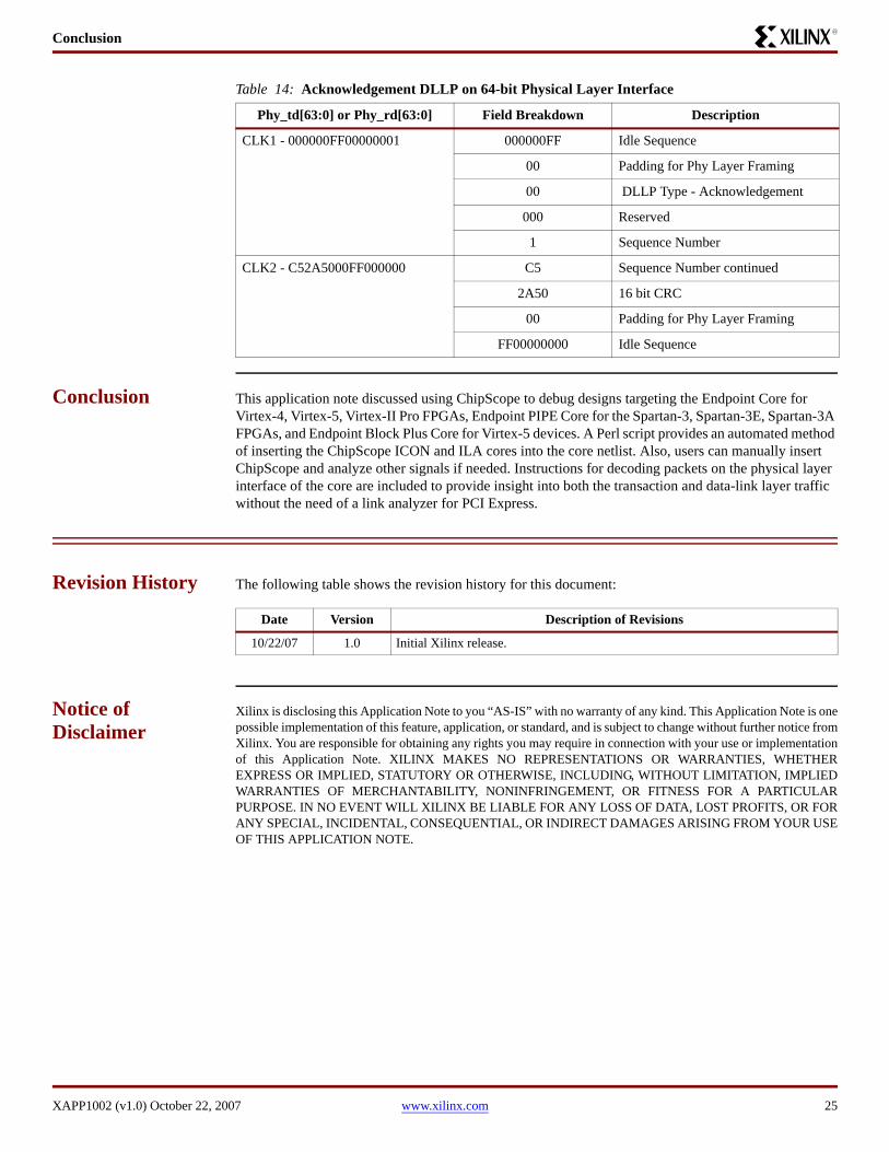
Figure 23 shows an Acknowledgement (ACK) DLLP in the ChipScope analyzer waveform.
Table 14 breaks down the ACK DLLP shown in Figure 23. The ACK packet begins on the lower half of the 64-bit bus as indicated by phy_rframe_l changing. Since phy_rctrl_l remains de-asserted, the packet is either a DLLP or IDLE. IDLEs are indicated by values of either 000000FF or FF000000. In this case, the packet is a DLLP. The ACK DLLP ends on the next clock cycle on the upper 32-bits of the data bus. This is indicated by phy_rframe_l changing from high to low to indicate the beginning of a new packet on the lower 32-bits. In this case, the new packet is an IDLE sequence.
Table 13: Memory Read 32-bit on 64-bit Physical Layer Interface
Phy_td[63:0] or Phy_rd[63:0] Field Breakdown Description
CLK1 - 000000FF00068500 000000FF IDLE Sequence
00 Padding for Phy Layer Framing
0685 Sequence Number
00 Fmt/Type - Memory Read 32 bit
CLK2 - 0000010000110FFF 0 Traffic Class
0 Reserved
0 TD (TLP Digest), EP (TLP Poisoned), Attr (Attributes)
001 Length
0000 Requestor ID
11 Tag
0 Last DW byte enable
F First DW byte enable
FF 32 bit address
CLK3 - 4F00201D1A305700 4F0020 Address Continued
1D1A3057 CRC
00 Padding
Figure 23: ChipScope Capture of Acknowledgement DLLP on Physical Layer Interface
X1002_24_081007
Conclusion
XAPP1002 (v1.0) October 22, 2007 www.xilinx.com 25
R
Conclusion This application note discussed using ChipScope to debug designs targeting the Endpoint Core for Virtex-4, Virtex-5, Virtex-II Pro FPGAs, Endpoint PIPE Core for the Spartan-3, Spartan-3E, Spartan-3A FPGAs, and Endpoint Block Plus Core for Virtex-5 devices. A Perl script provides an automated method of inserting the ChipScope ICON and ILA cores into the core netlist. Also, users can manually insert ChipScope and analyze other signals if needed. Instructions for decoding packets on the physical layer interface of the core are included to provide insight into both the transaction and data-link layer traffic without the need of a link analyzer for PCI Express.
Revision History The following table shows the revision history for this document:
Notice of Disclaimer
Xilinx is disclosing this Application Note to you “AS-IS” with no warranty of any kind. This Application Note is onepossible implementation of this feature, application, or standard, and is subject to change without further notice fromXilinx. You are responsible for obtaining any rights you may require in connection with your use or implementationof this Application Note. XILINX MAKES NO REPRESENTATIONS OR WARRANTIES, WHETHEREXPRESS OR IMPLIED, STATUTORY OR OTHERWISE, INCLUDING, WITHOUT LIMITATION, IMPLIEDWARRANTIES OF MERCHANTABILITY, NONINFRINGEMENT, OR FITNESS FOR A PARTICULARPURPOSE. IN NO EVENT WILL XILINX BE LIABLE FOR ANY LOSS OF DATA, LOST PROFITS, OR FORANY SPECIAL, INCIDENTAL, CONSEQUENTIAL, OR INDIRECT DAMAGES ARISING FROM YOUR USEOF THIS APPLICATION NOTE.
Table 14: Acknowledgement DLLP on 64-bit Physical Layer Interface
Phy_td[63:0] or Phy_rd[63:0] Field Breakdown Description
CLK1 - 000000FF00000001 000000FF Idle Sequence
00 Padding for Phy Layer Framing
00 DLLP Type - Acknowledgement
000 Reserved
1 Sequence Number
CLK2 - C52A5000FF000000 C5 Sequence Number continued
2A50 16 bit CRC
00 Padding for Phy Layer Framing
FF00000000 Idle Sequence
Date Version Description of Revisions
10/22/07 1.0 Initial Xilinx release.