Embed Size (px)
Citation preview

Revista Latinoamericana de Metalurgia y Materiales, al. 19, 1999, 7-12
APPLICATION OF SEM TO THE STUDY OF CERAMICSURFACES
N. Ravishankar and C. Barry Carter
Department of Chemical Engineering and Materials Science, University of Minnesota421 Washington Ave SE, Minneapolis, MN 55455-01432
Abstraet
Scanning electron microscopy is a particularly suitable technique for studying surfaces of ceramics.For these materials, an improved understanding of processing requires a greater knowledge of thestructure of surfaces at a sub-micron level. High spatial resolution, combined with analytical capabilityand relative ease of sample preparation, makes SEM an ideal technique for the study of surfaces. Thedewetting of liquids on single-crystal substrates, the crystallization of glass on surfaces and thebehavior of the liquids in grain boundaries are examples of such studies that are presented in this paperto bring out the versatility of the technique in studying different kinds of interfacial phenomena.
Keywords: scanning electron microscopy, high spatial resolution, surface, ceramics
Resumen
La microscopía electrónica de barrido es una técnica particularmente apropiada para el estudio desuperficies cerámicas. Para estos materiales, un entendimiento mejorado del proceso requiere un mayorconocimiento de la estructura de la superficie a un nivel submicrométrico. La alta resolución espacial,combinada con la capacidad analítica y una relativamente fácil preparación de la muestra, hacen de laMEB una técnica ideal para el estudio de superficies. La no mojabilidad de líquidos sobre substratos decristales simples, la cristalización de vidrio sobre superficies y el comportamiento de los líquidos en losbordes de grano son ejemplos de estos estudios que se presentan en este trabajo para mostrar laversatilidad de la técnica en el estudio de los diferentes tipos de fenómenos interfaciales.
Palabras clave: microscopia electrónica de barrido, alta resolución, superficies, cerámicas
1. Introduction
Ceramic oxides constitute one of the most importantclass of materials and exhibit a wide range of properties.The processing of ceramics (particularly liquid-phasesintering) frequently involves solid-Iiquid interactionsthat are not fully understood. Microstructural examinationof these interactions in model systems can shed light onmany of the complex processes that occur in a realmaterial. In most cases, the surface structure andmorphology dictate the behavior and hence it is importantto study the surface topography at a high resolution,
Scanning electron microscopy (SEM) is used in thesecondary-electron (SE) imaging mode to image surfacetopography. Recent advances in electron optics and lens
design have enabled surface spatial resolution thatapproaches the resolution obtainable from a conventionalTEM [1]. The resolution depends directly on the probesize; such a small probe size which still has sufficientcurrent is achievable using a field-emission gun as theelectron source. The use of lower accelerating voltagesreduces the interaction volume and improves theresolution in topography. The focal length of the probe-forming lens can be significantly lowered to the order ofmillimeters so as to minimize spherical aberrations. In thepresent generatíon of in-the-Iens SEMs, the lens field isused to collect the secondary electrons onto a detectorplaced just above the lens so that the collection efficiencyis vastIy improved. A high signal-to-noise Autrata

surfaces is well kn..,?wn[2,3]. In particular, the faceting ofthe m-plane (10 1O, the first-order prism plane) ofsapphire has been studied in great detail. This plane isunstable and can reconstruct in to {1011} and {lO12}facets, which intersect along a < 1210> direction.
When the length scale of faceting is of the order of thesize of the droplets on the surface, interesting types ofsolid-Iiquid interactions take place [4-7]. The use ofFESEM at low voltages (-5 kV) provides suitableresolution for studying these interactions.
Figure 1 is a secondary-electron (SE) image of a dewetdroplet on the m-plane of sapphire. The sample wasannealed at 1700°C for 7h. The faceting ofthe substrate isseen clearly. The height ofthe facets is ofthe order oftensof nanometers. The facets intersect along a < 112 O>direction, i.e., the straight lines that ate seen are parallel tothis direction. The cross-section ofthe liquid droplet is notcircular in this case The facets on the surface are alsoaffected by the presence of the liquid. The facetingbehavior of the alumina surface in the presence of glasshas been studied earlier. The liquid preferentially wets onetype of facet on the surface. There is a significant bendingof the steps in the vicinity of the solid-liquid-vapor(SL V) triple-junction
8 N Ravishankar y e: B. Carter/Revi~ta Latinoamericana de Metalurgia y Materiales.
backscattered detector gives excellent backscatteredelectron (BSE) resolution at low voltages. The SEM wascarried out in a Hitaohi 8-=900· field-emission SEM(FESEM). The microscope has an immersiorrobjectivelens with the SE resolution capability of O.7nm al -an ..accelerating voltage of30kV (about 3nm at 3kV).
2. Experimental
In the present study, the alumina (Ah03)/anorthite(CaAl2Si208) system is chosen as a model system toexamine many of -the interesting aspects of solid-liquidinteractions. In particular, the following aspects have beenstudied. The process of dewetting of liquids on solidsubstrates depends on the roughness of the surface.Reconstruction of high-index surfaces produces a steppedstructure with the size of the steps of the order of a fewten s of nanometers. When the dimensions of the liquiddroplet is of the order of the length scale of faceting,additional interesting interactions can occur. The study ofsuch surfaces using an FESEM provides insight into thewetting behavior on stepped surfaces
The stability of liquid films in grain boundaries (GB)is dictated in part by the relative values of the energies ofthe grain boundary and the free surface. Under conditionswhere the Jiquid wets the surface and does not wet theGB, the liquid can migrate out of the GB. SEMinvestigation 011 the migration of liquid from grainboundaries can clarify many of the important aspects of
•the mechanistics of the liquid-phase sintering process.The crystallization of silicate glass on crystallinesubstrates is also dictated by the orientation and surfacestructure. The crystaIlized phase usuaIly forms byheterogeneous nucleation on the substrate. The faceting ofthe underlying substrate also plays an important role indetermining the morphology of the crystallized phase. .
'1
3. Results and Discussion
3. J Dewetting ofAnorthite on Sapphire Surfaces
The surface energy of a liquid is isotropic(independent of orientation) and hence a liquid dropletassumes a spherical shape to minimize the total surfaceenergy of the system. For a liquid droplet on a flat,isotropic substrate, the shape corresponding to theminimum in energy can be described as spherical cap (acircular cross-section). The presence of a surface structure(ledges, for instance) can alter the shape of the liquiddroplet.
The equilibrium shape of a solid is geometricallysimilar to the shape obtained by the Wulff construction onthe .polar plot of-the surface energy (the v-plot). Surfacesthat appear in the Wulff shape are those with theIowestenergy. Herring's theorem states that any surface which isnot a partof the Wulff shape (high-index, higher energyplanes) will reconstruct into a hill-and-vaIley structurecomprising the low-energy facets. Edge effects aréneglected. The reconstruction of high-index sapphire
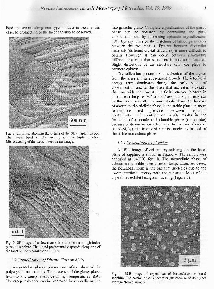
Fig. l. SE image of a dewet droplet of anorthite on areconstructed m-planeof sapphire. The m-plane reconstructs into{1011} and {lO12} facets during the high-temperature anneaI.The liquid tends to wet one type offacet in the stepped structure.
Figure 2 is an SE image showing the details of theSLV triple junction. The facets bend and break down intomicrofacets; they themselves facet. The glass pocket isflattened on one .side indicating that the liquidpreferentiaIly wets one .type of facet in the steppedstructure [4,6]. Figure 3 is an SE image of a dewet dropleton a high-index plane of sapphire. The tendency of the
Revista Latinoamericana de Metalurgia y Material. • ~ _ 19. 1999 9
liquid to spread aIong one type of facet is seen in thiscase. Microfaceting ofthe facet can also be observed.
Fig. 2. SE image showing the details of the SLV triple junction.The facets bend in the vicinity of the triple junction.Microfaceting of the steps is seen in the image,
Fig, 3. SE image of a- dewet anorthite droplet on a high-indexplane of sapphire. The liquid preferentially spreads along one ofthe facet on the reconstructed surface.
3.2 Crystallizatian afSilicate Glass an A 1203
Intergranular glassy phases are often observed inpolycrystalline ceramics. The presence ofthe glassy phaseleads to low creep resistance at high temperatures [8,9].The creep resistance can be improved by crystallizing the
intergranular phase. Complete _ o the glassyphase can be obtained by 2 the glasscomposition and by promoting epi _.szañizarion[10]. Epitaxy relies on the matching 0-1- . etersbetween the two phases. Epitaxy berween armaterials (different crystal structures) is more - toobtain. However, it can occur between strucnnallydifferent material s that share certain structural feamres.Slight distortions of the structure can take place topromote epitaxy.
Crystallization proceeds via nucleation of the crystalfrom the glass and its subsequent growth. The interfacialenergy term dominates during the early stage ofcrystallization and so the phase that nucleates is usualIythe one with the lowest interfacial energy (c1osest instructure to the parent/substrate phase) although it may notbe thermodynamically the most stable phase. In the caseof anorthite, the triclinic phase is the stable phase at roomtemperature and pressure. However, epitacticcrystallization of anorthite on Ab03 results in theformation of a pseudo-orthorhombic phase (o-anorthite)because of its nucleation advantage. In the case of celsian(BaAhSi20g), the hexacelsian phase nucleates instead ofthe stable monoclinic phase.
3. 2. J Crysta!lizatian af Celsian
A BSE image of celsian crystallizing on the basalplane of sapphire is shown in Figure 4. The sample wasannealed at 1400°C for 1h. The monoclinic phase ofcelsian is the stable form at room temperature. However,the hexagonal form is the one that nucleares due to thelower interfacial energy with the substrate. Most of thecrystallites exhibit hexagonal faceting (Figure 5).
Fig. 4. BSE image of crystallites of hexacelsian on basalsapphire. The celsian phase appears bright because of its higheraverage atomic number.
· Ravishankar y C. B. Carter/Revista Latinoamericana de Metalurgia y Materiales.
Fig.5. An SE image of a sample of celsian on basal sapphirc thathas been heat treated at l200°C for 20h. The hexagonal facetingof the precipitates is much more pronounced in this case.
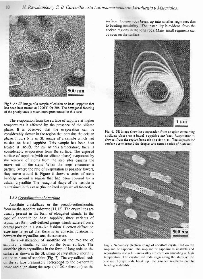
The evaporationfrom the surface of sapphire at highertemperatures is affected by the presence of the silicatephase. It is observed that the evaporation can beconsiderably slower in the region that contains the celsianphase. Figure 6 is an SE image of a sample which hadcelsian on basal sapphire. This sample has been heattreated at 1850°C for 2h. At this temperature, there isconsiderable evaporation from the surface. The exposedsurface of sapphire (with no silicate phase) evaporates bythe removal of atoms from the step sites causing themovement of the steps. When the steps encounter aparticle (where the rate of evaporation is possibly lower),they curve around it. Figure 6 shows a series of stepsoending around a region that had .been covered by acelsian crystallite. The hexagonal shape of the particle ismaintained in this case (the inclined steps are all faceted).
3.2.2 Crystallization ofAnorthite
Anorthite crystallizes in the pseudo-orthorhornbicform on the sapphire substrate [I 1,12]. The crystallites areusually present in the form of elongated islands. In thecase of anorthite on basa) sapphire, three variants ofcrystallites form well-defined groups which radiate from acentra) position in a star-like fashion. Electron diffractionexperiments reveal that there is an epitactic reiationshipbetween the crystallites and the substrate.
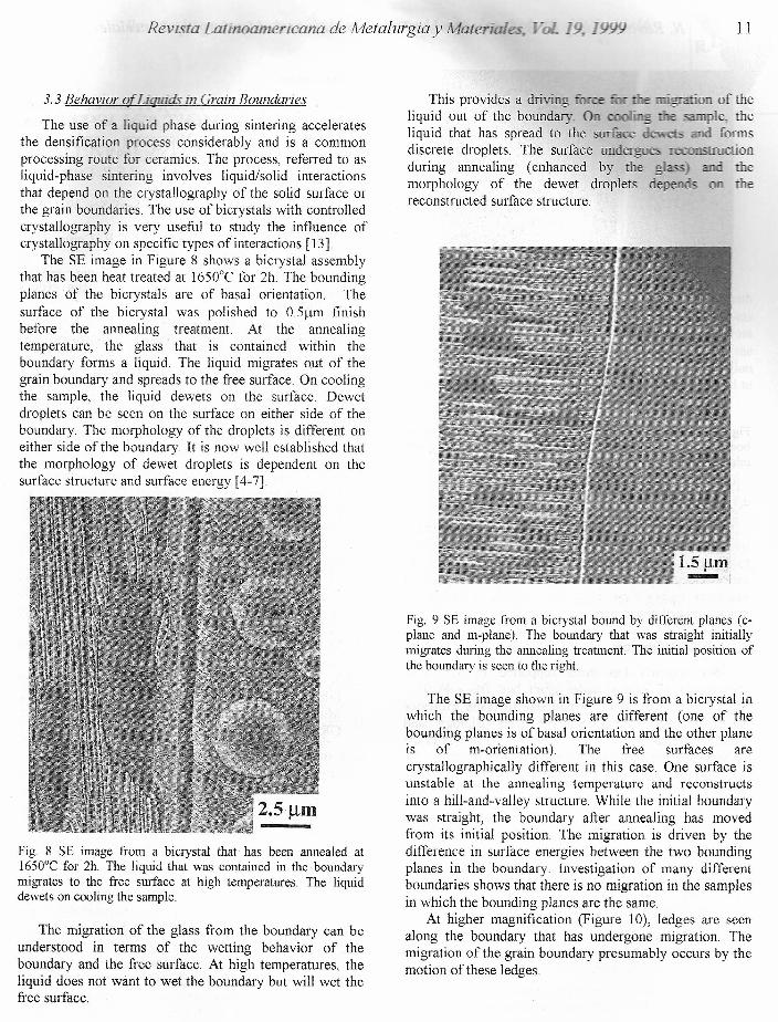
The crystallization of anorthite on the m-plane ofsapphire is similar to that on the basal surface. Theanorthite glass crystallizes in the form of long rods on thesurface as shown in the SE image of crystallized anorthiteon me m-plane of sapphire (Fig. 7). The crystallized rodson the surface presumably correspond to the o-anorthitephase and align along the steps « 1120> direction) on the
surface. Loa er rods break up intosmaller segments dueto beading instability. The instability is evident from thenecked regions in the long rods. Many small segments canbe seen on the surface.
Fig. 6. SE irnage showing evaporation from a region contaíninga silicate phase on a basal sapphire surface. Evaporation isslowest frorn the region bene ath th e droplet. The steps on thesurface curve around the droplct and form a series of plateaus.
Fig. 7. Secondary electron image of anorthite crystallized on them-plano of sapphire. The m-plane of sapphire is unstable andreconstructs into a hill-and-valley structure on anncaling al highternperature. The crystallizcd rods align along the steps on thesurface. Longer rods break up into smaller segments due tobeading instability.
Revista Latinoamericana de Metalurgia y Material
3.3 Behavior o{Liguids in Grain Boundaries
The use of a liquid phase during sintering acceleratesthe densification process considerably and is a commonprocessing route for ceramics. The process, referred to asliquid-phase sintering involves liquid/solid interactionsthat depend on the crystallography of the salid surface orthe grain boundaries. The use of bicrystals with controlledcrystallography is very useful to study the influence ofcrystallography on specific types of interactions [13].
The SE image in Figure 8 shows a bicrystal assemblythat has been heat treated at 1650°C for 2h. The boundingplanes of the bicrystals are of basal orientation. Thesurface of the bicrystal was polished to 0.51lm finishbefore the annealing treatment. At the annealingtemperature, the glass that is contained within theboundary forms a liquido The liquid migrates out of thegrain boundary and spreads to the free surface. On coolingthe sample, the liquid dewets on the surface. Dewetdroplets can be seen on the surface on either side of theboundary. The morphology of the droplets is different oneither side of the boundary. It is now well established thatthe morphology of dewet droplets is dependent on thesurface structure and surface energy [4-7].
Fig. 8 SE image from a bicrystal that has been annealed at1650°C for 2h. The liquid that was contained in the boundarymigrates to the free surfaee at high temperatures. The liquiddewets on eooling the sample.
The migration of the glass from the boundary can beunderstood in terms of the wetting behavior of theboundary and the free surface. At high temperatures, theliquid does not want to wet the boundary but will wet thefree surface.
19. 999 11
This provides a driving force - ion of theliquid out of the boundary. On _ sample, theliquid that has spread to the surface dewers and formsdiscrete droplets. The surface undergoes ctionduring annealing (enhanced by the g I themorphology of the dewet droplets depends on mereconstructed surface structure.
Fig. 9 SE image from a bierystal bound by different planes (e-plane and m-plane). The boundary that was straight initiallymigrates during the annealing treatment. The initial position ofthe boundary is seen to the right.
The SE image shown in Figure 9 is from a bicrystal inwhich the bounding planes are different (one of thebounding planes is of basal orientation and the other planeis of m-orientation), The free surfaces arecrystallographically different in this case. One surface isunstable at the annealing temperature and reconstructsinto a hill-and-valley structure. While the initial boundarywas straight, the boundary after annealing has movedfrom its initia! position. The migration is driven by thedifference in surface energies between the two boundingplanes in the boundary. Investigation of many differentboundaries shows that there is no migration in the samplesin which the bounding planes are the same.
At higher magnification (Figure 10), ledges are seenalong the boundary that has undergone migration. Themigration of the grain boundary presumably occurs by themotion ofthese ledges

~~Ravishankar y C. B. Carter/Revista Latinoamericana de ]t{etalurgia y Materiales.
Fig. lO. Higher magnification SE image from a migrated grainboundary. The presence of ledges is seen. The boundarymigration is due to the motion ofthese ledges at the boundary.
4. Conclusions
It is seen that the field-emission SEM is an extremelyuseful and poweiful tool to study various problems relatedto surfaces of ceramic materials. The relative ease ofsarnple preparation and the high resolution of modernmachines makes them ideal for studying a variety ofsurface-related phenomena.
S. Acknowledgments
This research has been supported by the U.S.Department of Energy under grant No. DE - FG02 -92ER45465. The authors would like to thank ProfessorStan Erlandsen, Department of Cell Biology andNeuroanatomy, University of Minnesota for access to theFESEM and Chris Frethem for technical assistance.
6. References
l. 1.1. Goldstein, D.E. Newbury P. Echlan, D.C. Joy,A.D. Romig, C.E. Lyman, C. Fiori, and E. Lifshin,Scanning Electron Microscopy and X-rayMicroanalysis, Plenum Press, NY, 1992.
2. J.R. Heffelfinger, M.W. Bench, and C.B. Carter, Surf.Sci. Lett. 343-, (1995) pp. 1161-66.
3. J.R. Heffelfinger and c.B. Carter, Surf. Sci. 39, (1997)pp. 188-200
4. S. Ramamurthy, B.C. Hebert, and c.B. Carter, Phil.Mag. Lett. 72, (1995) pp. 269-75.
5. S. Ramamurthy, B.C. Hebert, c.n. Carter, and H.Schmalzried, Mat. Res. Soco Symp. Proc. 398, (1996)pp. 295-300
6. S. Ramamurthy, .Amorphous-Crystalline Interfaces inOxide-Ceramics, Ph.D. Thesis, University ofMinnesota (1996).
7. N. Ravishankar, S. Ramamurthy, H. Schmalzried, andC.B. Carter in Wetting of Anorthite Liquid on m-Sapphire Substrates, Microscopy and Microanalysis'99, Springer, Portland, OR, pp. 812-813.
8. D.R. Clarke, Ann. Rev. Mater. Sci. 17, (1987) pp. 57-74
9. D.R. Clarke in Intergranular Phases in PolycrystallineCerarnics, edited by L.-c. Dufour, C. Monty, and G.Petot-Ervas, Kluwer Academic Publishers, Dordrecht,(1989) pp. 57-79.
10. N.P. Padture and H.M. Chan, J. Mater. Res. 7, (1992)pp. 170-177
11. M. P. Mallamaci, J. Bentley and C. B. Carter in In-situCrystallization of Silicate Glass Films Deposited Ona-Ah03, 51st Annual Meeting of Microscopy Societyof America, San Francisco Press, 928-929.
12. M. P. Mallamaci, 1. Bentley and C. B. Carter, ActaMater, 46(1), (1998) pp 283-303
13. N. Ravishankar and C.B. Carter in Migration ofSilicate Liquids out of Grain Boundaries in Ceramics,Microscopy and Microanalysis '99, Springer, Portland,OR, pp. 800-801. .