Embed Size (px)
Citation preview
Venu Menon Vice President,
Analog Technology Development
March 20, 2012
Applications Drive Analog Technology Development and Innovation
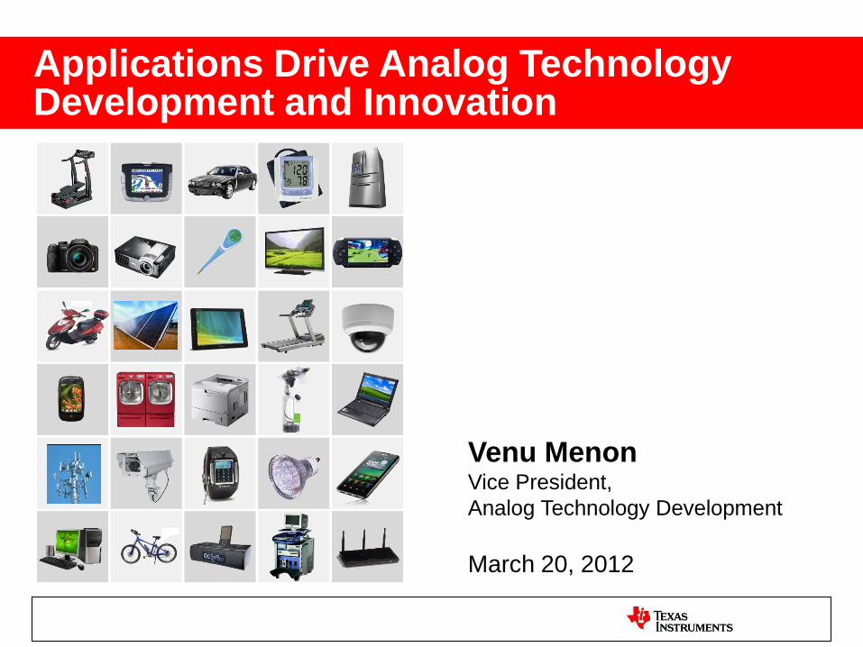
Inside the box
What can you do with these?
Nothing. Without analog!
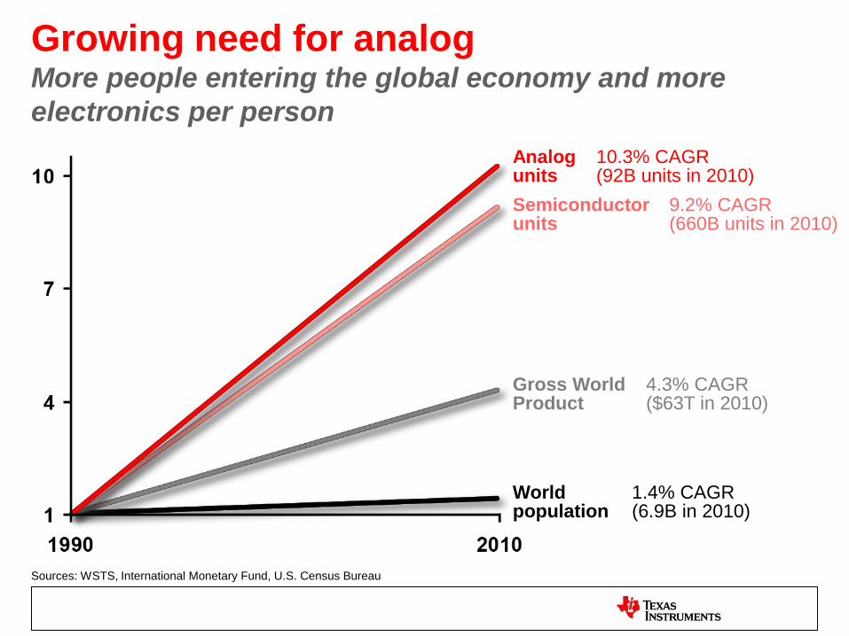
Growing need for analog More people entering the global economy and more
electronics per person
4.3% CAGR ($63T in 2010)
1.4% CAGR (6.9B in 2010)
Gross World Product
World population
Analog units
9.2% CAGR (660B units in 2010)
Sources: WSTS, International Monetary Fund, U.S. Census Bureau
10.3% CAGR (92B units in 2010)
Semiconductor units
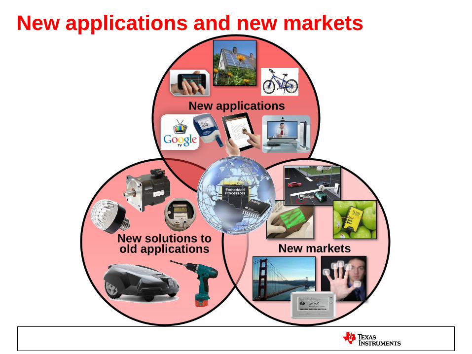
New applications and new markets
New applications
New solutions to old applications New markets
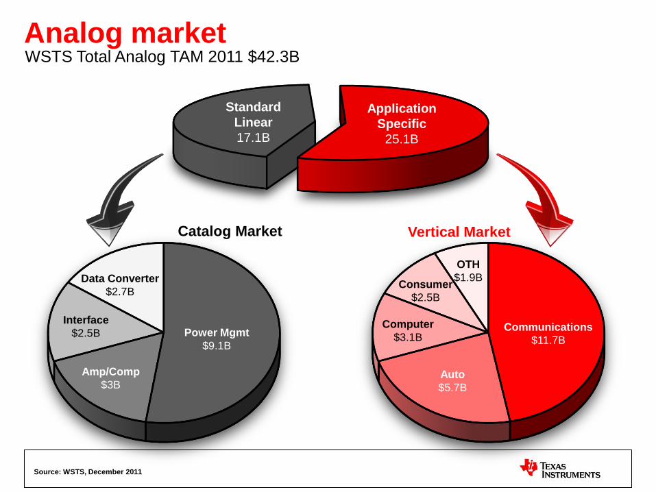
Source: WSTS, December 2011
Analog market WSTS Total Analog TAM 2011 $42.3B
Vertical Market Catalog Market
Standard
Linear
17.1B
Application
Specific
25.1B
Power Mgmt
$9.1B
Data Converter
$2.7B
Amp/Comp
$3B
Interface
$2.5B Communications
$11.7B
Auto
$5.7B
Computer
$3.1B
Consumer
$2.5B
OTH
$1.9B
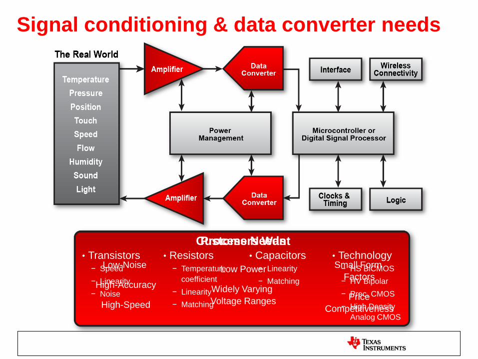
Signal conditioning & data converter needs
• Transistors − Speed
− Linearity
− Noise
• Resistors − Temperature
coefficient
− Linearity
− Matching
• Capacitors − Linearity
− Matching
• Technology − HS BiCMOS
− HV Bipolar
− Prec. CMOS
− High Density
Analog CMOS
Low-Noise
High-Accuracy
High-Speed
Customers Want
Small Form
Factors
Price
Competitiveness
Low Power
Widely Varying
Voltage Ranges
Process Needs
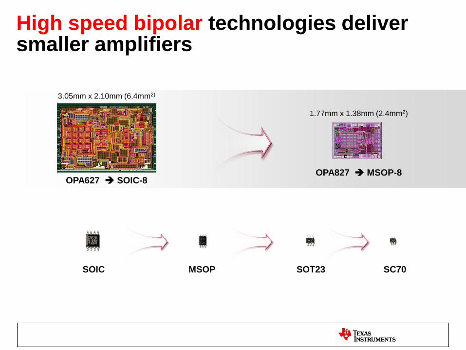
High speed bipolar technologies deliver smaller amplifiers
SOIC SOT23 MSOP SC70
OPA627 SOIC-8
3.05mm x 2.10mm (6.4mm2)
OPA827 MSOP-8
1.77mm x 1.38mm (2.4mm2)
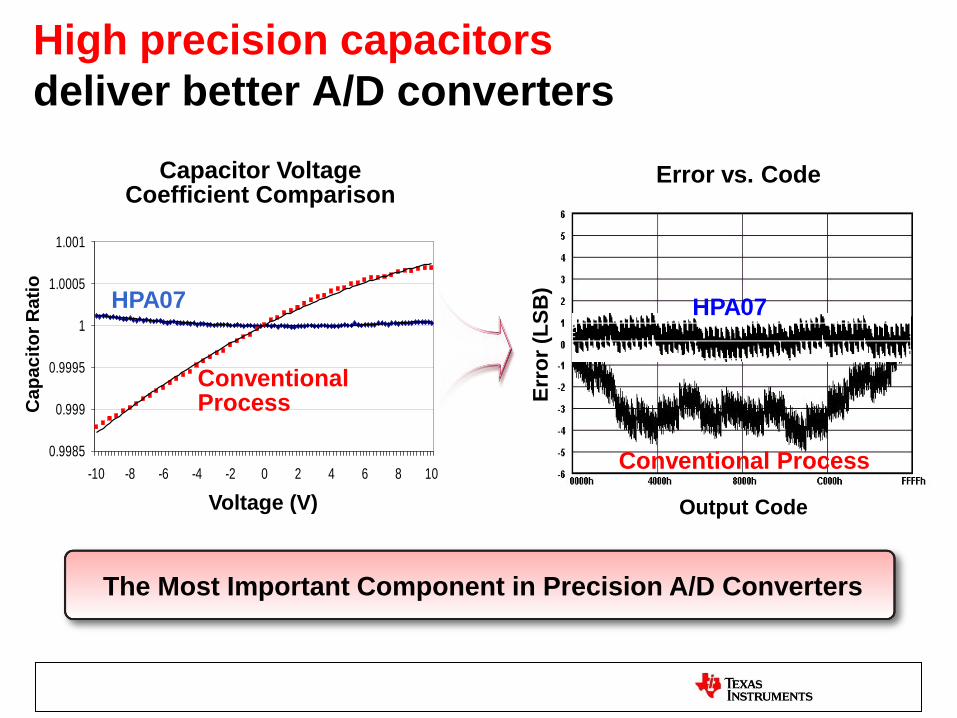
High precision capacitors
deliver better A/D converters
Capacitor Voltage Coefficient Comparison
0.9985
0.999
0.9995
1
1.0005
1.001
-10 -8 -6 -4 -2 0 2 4 6 8 10
V (v)
HPA07
Conventional Process
Voltage (V)
Ca
pa
cit
or
Ra
tio
The Most Important Component in Precision A/D Converters
Conventional Process
HPA07
Output Code
Error vs. Code
Err
or
(LS
B)
DAC8534 & DAC8554 Channel C INL Error vs.
DIGITAL INPUT CODE
-48
-32
-16
0
16
32
48
IN
L (L
SB
)
DAC8534 - Channel C
DAC8554 - Channel C
VDD=VREF=5V, TA=25C,
Channel C Output
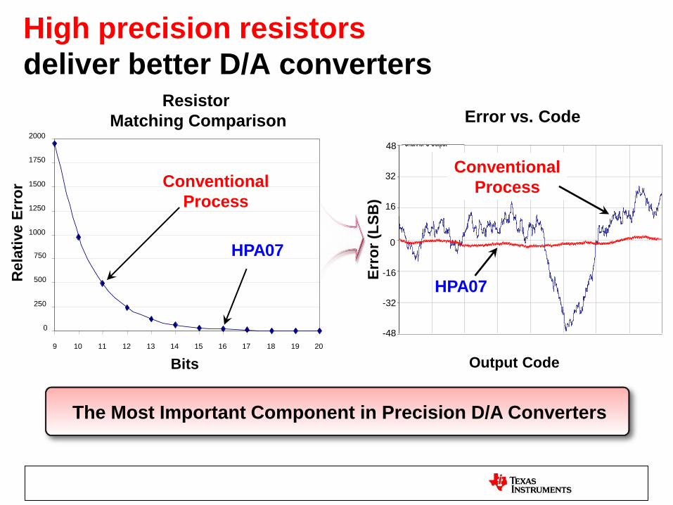
High precision resistors
deliver better D/A converters
0
250
500
750
1000
1250
1500
1750
2000
9 10 11 12 13 14 15 16 17 18 19 20
Bits
Rela
tive E
rro
r
HPA07
Conventional
Process
Resistor
Matching Comparison
The Most Important Component in Precision D/A Converters
Error vs. Code
48
32
16
0
-16
-32
-48
Err
or
(LS
B)
Output Code
HPA07
Conventional
Process
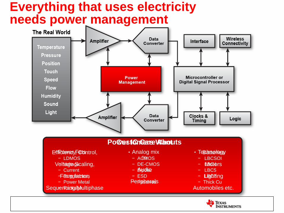
Everything that uses electricity needs power management
Efficiency, Control,
Voltage Scaling,
Form factor,
Sequencing/Multiphase
Customers Want
Batteries
Motors
Lighting
Automobiles etc.
In
Audio
Peripherals
Power IC Care Abouts
• Power Fets − LDMOS
− Voltage
− Current
− Ruggedness
− Power Metal
− Package
• Analog mix − ACMOS
− DE-CMOS
− Bipolar
− ESD
− Passives
• Technology − LBCSOI
− LBC4
− LBC5
− LBC7
− Thick Cu
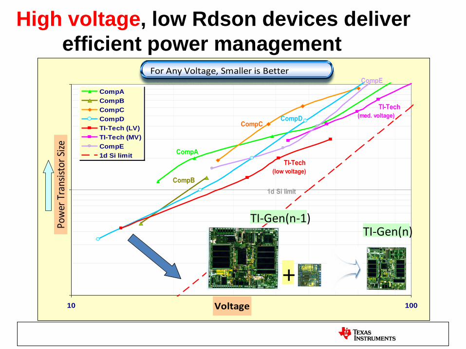
High voltage, low Rdson devices deliver
efficient power management
0.01
0.10
1.00
10 100Voltage
CompA
CompB
CompC
CompD
TI-Tech (LV)
TI-Tech (MV)
CompE
1d Si limit TI-Tech
(low voltage)
CompA
CompC
1d limit
CompD
CompE
CompB
1d Si limit
TI-Tech
(med. voltage)
For Any Voltage, Smaller is BetterPo
wer
Tra
nsis
tor
Size
+
TI-Gen(n-1) TI-Gen(n)
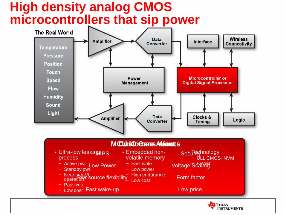
High density analog CMOS microcontrollers that sip power
Customers Want
MIPS
Low Power
Pwr source flexibility
Fast wake-up
Security
Voltage Scaling
Form factor
Low price
• Ultra-low leakage process − Active pwr − Standby pwr − Near sub-Vt
operation − Passives − Low cost
• Embedded non-volatile memory − Fast write − Low power − High endurance − Low cost
• Technology − ULL CMOS+NVM − FRAM
MCU IC Care Abouts
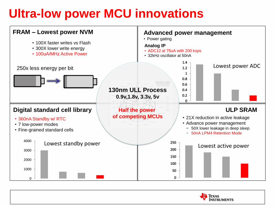
Ultra-low power MCU innovations
FRAM – Lowest power NVM
ULP SRAM Digital standard cell library
• 360nA Standby w/ RTC
• 7 low-power modes
• Fine-grained standard cells
• 21X reduction in active leakage
• Advance power management − 50X lower leakage in deep sleep
− 50nA LPM4 Retention Mode
Advanced power management • Power gating
Analog IP • ADC12 at 75uA with 200 ksps
• 32kHz oscillator at 50nA
• 100X faster writes vs Flash
• 300X lower write energy
• 100uA/MHz Active Power
Half the power
of competing MCUs
130nm ULL Process 0.9v,1.8v, 3.3v, 5v
0
1000
2000
3000
4000 Lowest standby power
0
0.2
0.4
0.6
0.8
1
1.2
1.4 Lowest power ADC
0
50
100
150
200
250 Lowest active power
250x less energy per bit
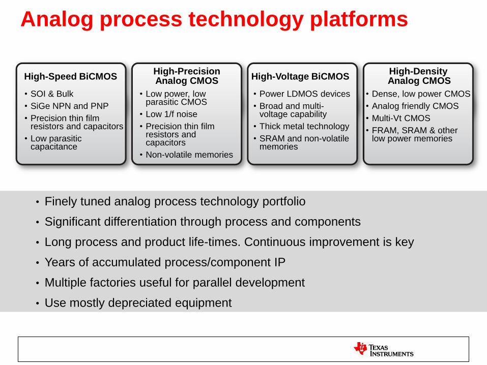
Analog process technology platforms
HPA07
High Precision
BiCom3
High Speed
LBC7
High Power
A035
High Density
• Finely tuned analog process technology portfolio
• Significant differentiation through process and components
• Long process and product life-times. Continuous improvement is key
• Years of accumulated process/component IP
• Multiple factories useful for parallel development
• Use mostly depreciated equipment
• SOI & Bulk
• SiGe NPN and PNP
• Precision thin film resistors and capacitors
• Low parasitic capacitance
High-Speed BiCMOS
• Low power, low parasitic CMOS
• Low 1/f noise
• Precision thin film resistors and capacitors
• Non-volatile memories
High-Precision Analog CMOS
• Dense, low power CMOS
• Analog friendly CMOS
• Multi-Vt CMOS
• FRAM, SRAM & other low power memories
High-Density Analog CMOS
• Power LDMOS devices
• Broad and multi-voltage capability
• Thick metal technology
• SRAM and non-volatile memories
High-Voltage BiCMOS
0
100,000
200,000
300,000
400,000
500,000
600,000
700,000
800,000
0 1 2 3 4 5 6 7 8 9 10 11 12 13 14 15
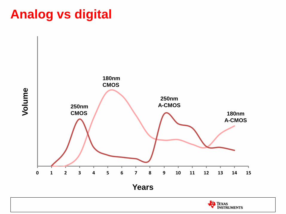
Analog vs digital
Years
Vo
lum
e
250nm
CMOS
180nm
CMOS
180nm
A-CMOS
250nm
A-CMOS
0
100,000
200,000
300,000
400,000
500,000
600,000
700,000
800,000
0 1 2 3 4 5 6 7 8 9 10 11 12 13 14 15
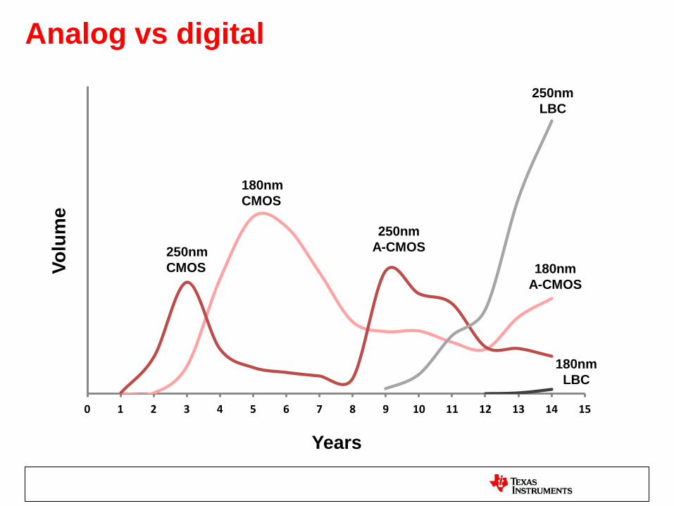
250nm
LBC
180nm
LBC
Analog vs digital
Years
Vo
lum
e
250nm
CMOS
180nm
CMOS
180nm
A-CMOS
250nm
A-CMOS
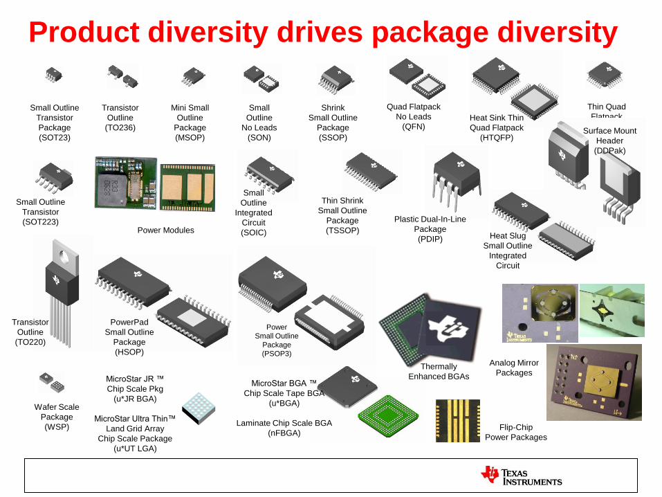
Product diversity drives package diversity
Quad Flatpack
No Leads
(QFN) Heat Sink Thin
Quad Flatpack
(HTQFP)
Small Outline
Transistor
(SOT223)
Thin Shrink
Small Outline
Package
(TSSOP)
Small
Outline
No Leads
(SON)
Wafer Scale
Package
(WSP)
Small Outline
Transistor
Package
(SOT23)
Thin Quad
Flatpack
(TQFP)
Transistor
Outline
(TO236)
PowerPad
Small Outline
Package
(HSOP)
Mini Small
Outline
Package
(MSOP)
Shrink
Small Outline
Package
(SSOP) Surface Mount
Header
(DDPak)
Transistor
Outline
(TO220)
MicroStar BGA ™
Chip Scale Tape BGA
(u*BGA)
Laminate Chip Scale BGA
(nFBGA)
Power
Small Outline
Package
(PSOP3)
Small
Outline
Integrated
Circuit
(SOIC) Heat Slug
Small Outline
Integrated
Circuit
MicroStar JR ™
Chip Scale Pkg
(u*JR BGA)
MicroStar Ultra Thin™
Land Grid Array
Chip Scale Package
(u*UT LGA)
Plastic Dual-In-Line
Package
(PDIP)
Analog Mirror
Packages Thermally
Enhanced BGAs
Flip-Chip
Power Packages
Power Modules
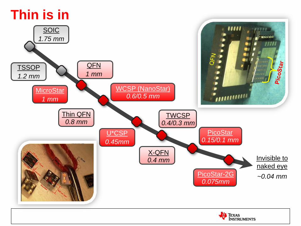
Thin is in
Invisible to
naked eye
~0.04 mm
QFN
1 mm
Thin QFN 0.8 mm
WCSP (NanoStar) 0.6/0.5 mm
X-QFN 0.4 mm
PicoStar 0.15/0.1 mm
TSSOP
1.2 mm
SOIC
1.75 mm
TWCSP 0.4/0.3 mm
MicroStar
1 mm
U*CSP
0.45mm
PicoStar-2G 0.075mm
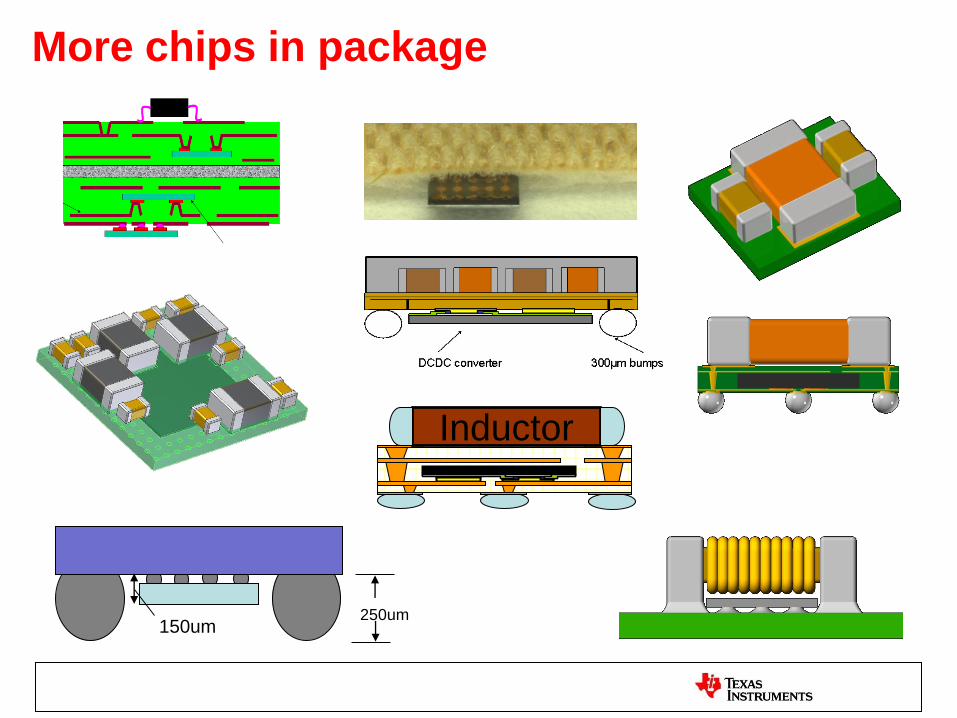
More chips in package
250um 150um
Inductor
Challenges & opportunities
• Not limited by an industry roadmap. Significant opportunities to differentiate. Creative ideas welcome!
• Managing large diversity of process technologies in many factories
• Years of accumulated process/component/design IP. Maintaining & updating processes, SPICE models, PDKs and documentation is a challenge.
• Leveraging older equipment and factories drives challenges with process matching. Must “copy smart”
• Speed boats, not aircraft carriers
Thank You!