Embed Size (px)
Citation preview

EE 330
Lecture 28
Small-Signal Model Extension
Applications of the Small-signal Model
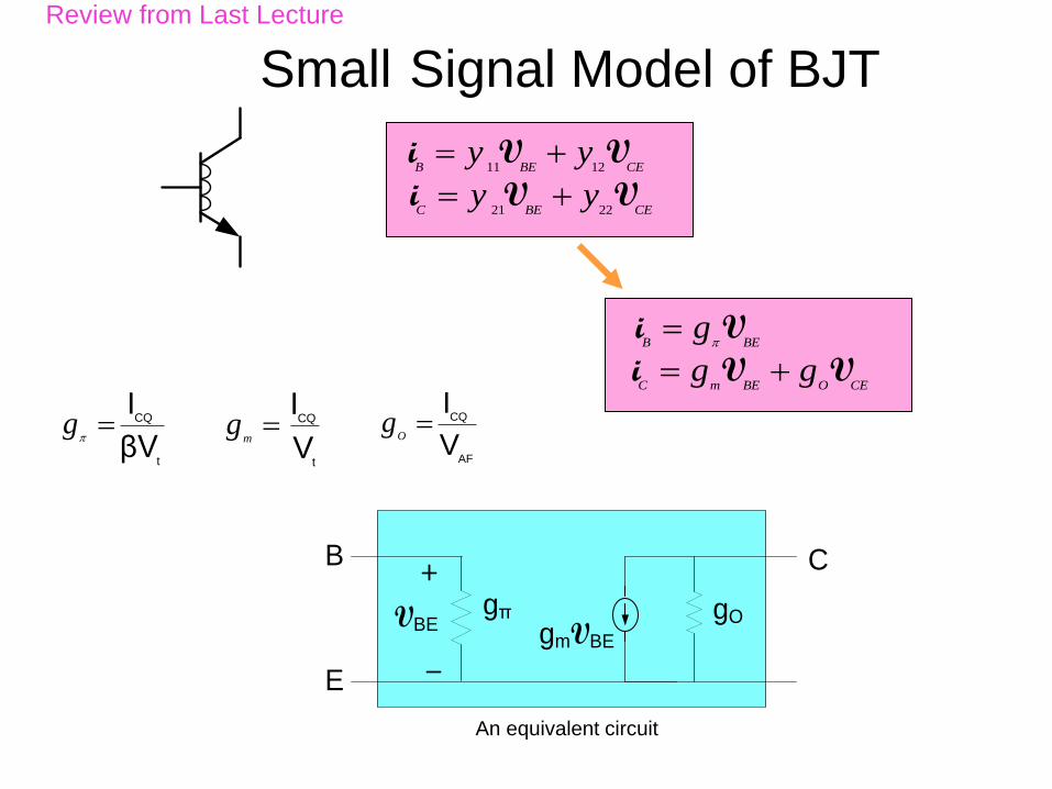
Small Signal Model of BJT
CQ
t
I
βVg
CQ
t
I
Vm
g CQ
AF
I
VO
g
21 22C BE CEy y i V V
11 12B BE CEy y i V V
C m BE O CEg g i V V
B BEg
i V
gOgmVBE
VBEgπ
B
E
C
An equivalent circuit
Review from Last Lecture
Small Signal BJT Model
B
E
C
Vbe
ic
gmVbego Vce
ib
gπ
t
CQm
V
Ig
t
CQ
βV
Ig
AF
CQ
V
Ig o
t
CQ
βV
Ig
AF
CQ
V
Ig o
B
E
C
Vbe
ic
go Vce
ib
gπbiβ
Alternate equivalent small signal model
Review from Last Lecture
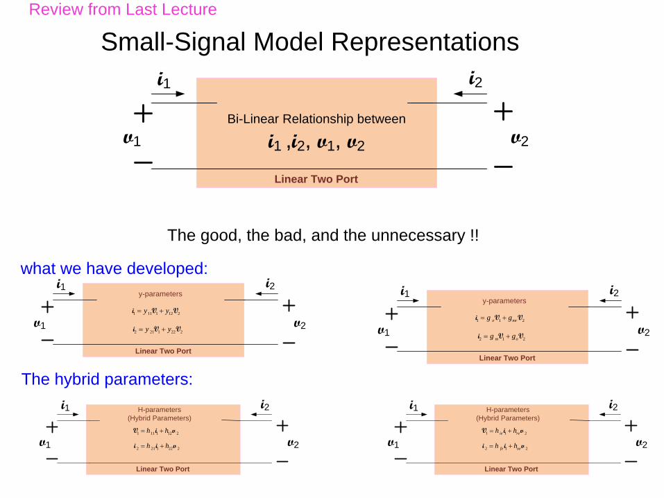
Bi-Linear Relationship between
i1 ,i2, v1, v2
i1
Linear Two Port
v1
i2
v2
Small-Signal Model Representations
The good, the bad, and the unnecessary !!
i1
Linear Two Port
v1
i2
v2
y-parameters
1 11 1 12 2y y i V V
2 21 1 22 2y y i V V
i1
Linear Two Port
v1
i2
v2
y-parameters
1 1 2mrg g i V V
2 1 2m og g i V V
i1
Linear Two Port
v1
i2
v2
H-parameters
(Hybrid Parameters)
1 11 1 12 2h h V i v
2 21 1 22 2h h i i v
i1
Linear Two Port
v1
i2
v2
H-parameters
(Hybrid Parameters)
1 1 2ie reh h V i v
2 1 2fe oeh h i i v
what we have developed:
The hybrid parameters:
Review from Last Lecture
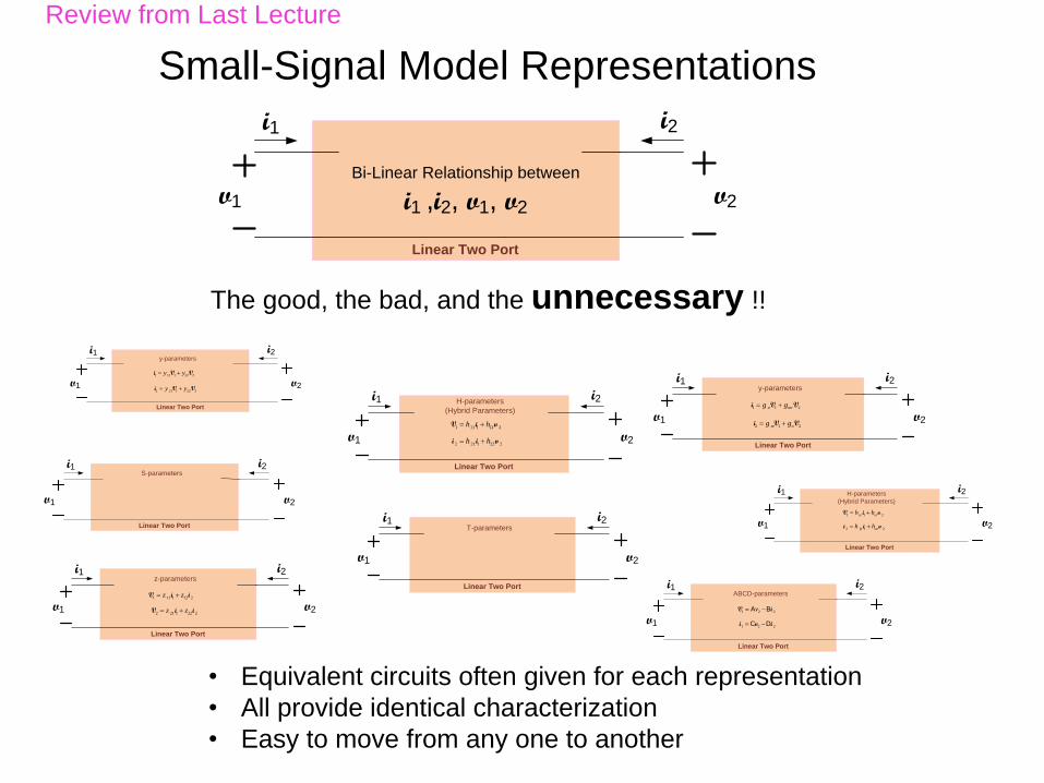
Bi-Linear Relationship between
i1 ,i2, v1, v2
i1
Linear Two Port
v1
i2
v2
Small-Signal Model Representations
The good, the bad, and the unnecessary !!
i1
Linear Two Port
v1
i2
v2
y-parameters
1 11 1 12 2y y i V V
2 21 1 22 2y y i V V
i1
Linear Two Port
v1
i2
v2
y-parameters
1 1 2mrg g i V V
2 1 2m og g i V V
i1
Linear Two Port
v1
i2
v2
H-parameters
(Hybrid Parameters)
1 11 1 12 2h h V i v
2 21 1 22 2h h i i v
i1
Linear Two Port
v1
i2
v2
H-parameters
(Hybrid Parameters)
1 1 2ie reh h V i v
2 1 2fe oeh h i i v
i1
Linear Two Port
v1
i2
v2
z-parameters
1 11 1 12 2z z V i i
2 21 1 22 2z z V i i
i1
Linear Two Port
v1
i2
v2
ABCD-parameters
1 2 2A Bv V i
1 2 2C D i v i
i1
Linear Two Port
i2
v2
S-parameters
v1
i1
Linear Two Port
i2
v2
T-parameters
v1
• Equivalent circuits often given for each representation
• All provide identical characterization
• Easy to move from any one to another
Review from Last Lecture

Active Device Model Summary What are the simplified dc equivalent models?
Simplified
Simplified
Simplified
Simplified
Simplified
0.6V
dc equivalent
G D
S
VGSQ 2OX
GSQ TnμC W
V -V2L
G D
S
VGSQ 2OX
GSQ TpμC W
V -V2L
B C
E
BQβI0.6V
IBQ
B C
E
BQβI0.6V
IBQ
Review from Last Lecture

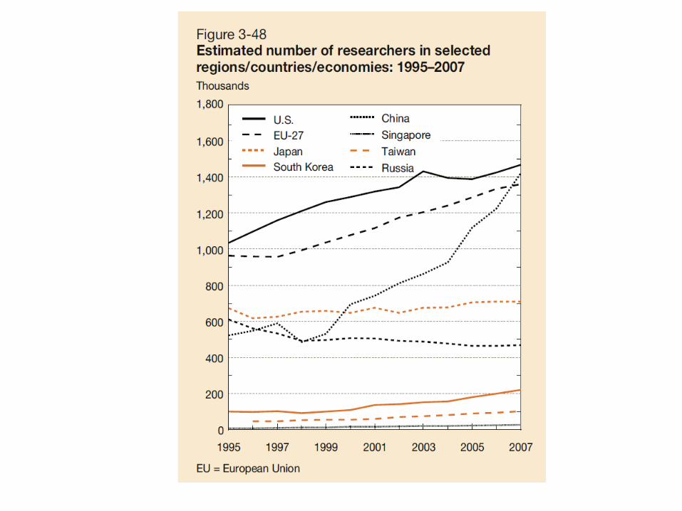
Engineering Trends and
Study Abroad Options


Engineers educated today will be under increasing pressure to be able to
communicate with, supervise, work with, and work for Asian engineers
that may or may not have good English communication skills and must
understand the culture of engineers around the world to be effective
This is not something that may happen in the future but rather is something that
is already occurring and WILL become increasingly critical in the next decade

The increasing role Asia is playing in both the engineering field and the world’s economy is unlike anything we have seen in many decades
All indicators suggest that this role will become even more significant in the future
Both opportunities and expectations in the field will invariable show increased alignment with business and engineering in a global economy
Understanding the culture and the environment of engineers working in Asia will offer substantial benefits for many/most engineers in the short-term and will likely be expected of many/most engineers within a decade
Study Abroad Opportunities
in Asia
Two Opportunities in Taiwan

Taipei 101 – The tallest building in the world !

Landmark Architecture – The Grand Hotel in Taipei
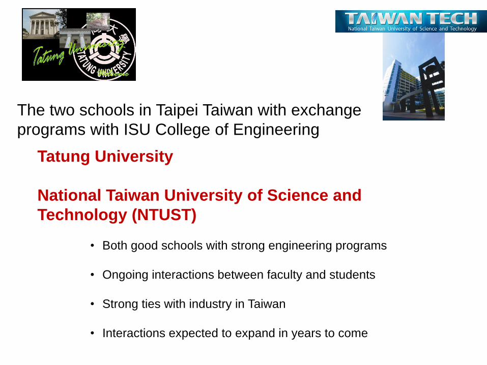
The two schools in Taipei Taiwan with exchange
programs with ISU College of Engineering
• Both good schools with strong engineering programs
• Ongoing interactions between faculty and students
• Strong ties with industry in Taiwan
• Interactions expected to expand in years to come
Tatung University
National Taiwan University of Science and
Technology (NTUST)

• Both schools will offer selected courses to ISU students in English
• Courses pre-approved so that progress towards graduation is not delayed
• Approximately revenue neutral exchange (often costs less than spending the time in Ames)
• Internship opportunity often provided
Exchange program principles:


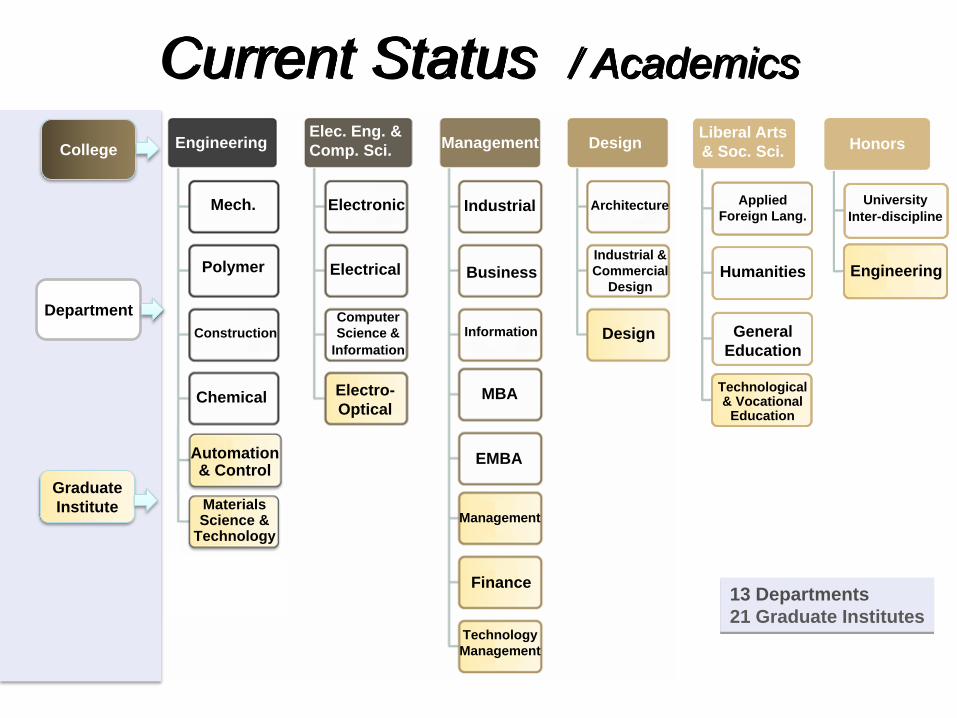
13 Departments
21 Graduate Institutes
College
Department
Graduate
Institute
Engineering Elec. Eng. &
Comp. Sci. Management Design
Liberal Arts
& Soc. Sci.
Mech.
Polymer
Construction
Chemical
Automation & Control
Materials Science &
Technology
Electronic
Electrical
Computer
Science &
Information
Electro-
Optical
Industrial
Business
Information
MBA
EMBA
Management
Finance
Technology
Management
Architecture
Industrial &
Commercial
Design
Design
Applied
Foreign Lang.
Humanities
General
Education
Technological & Vocational
Education
Honors
University
Inter-discipline
Engineering
Current Status / Academics
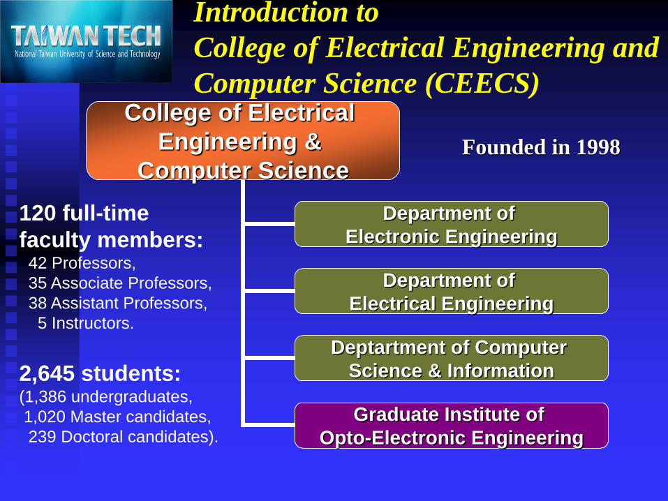
Introduction to
College of Electrical Engineering and
Computer Science (CEECS) College of Electrical
Engineering &
Computer Science
Department of
Electronic Engineering
Department of
Electrical Engineering
Deptartment of Computer
Science & Information
Graduate Institute of
Opto-Electronic Engineering
120 full-time
faculty members: 42 Professors,
35 Associate Professors,
38 Assistant Professors,
5 Instructors.
2,645 students: (1,386 undergraduates,
1,020 Master candidates,
239 Doctoral candidates).
Founded in 1998
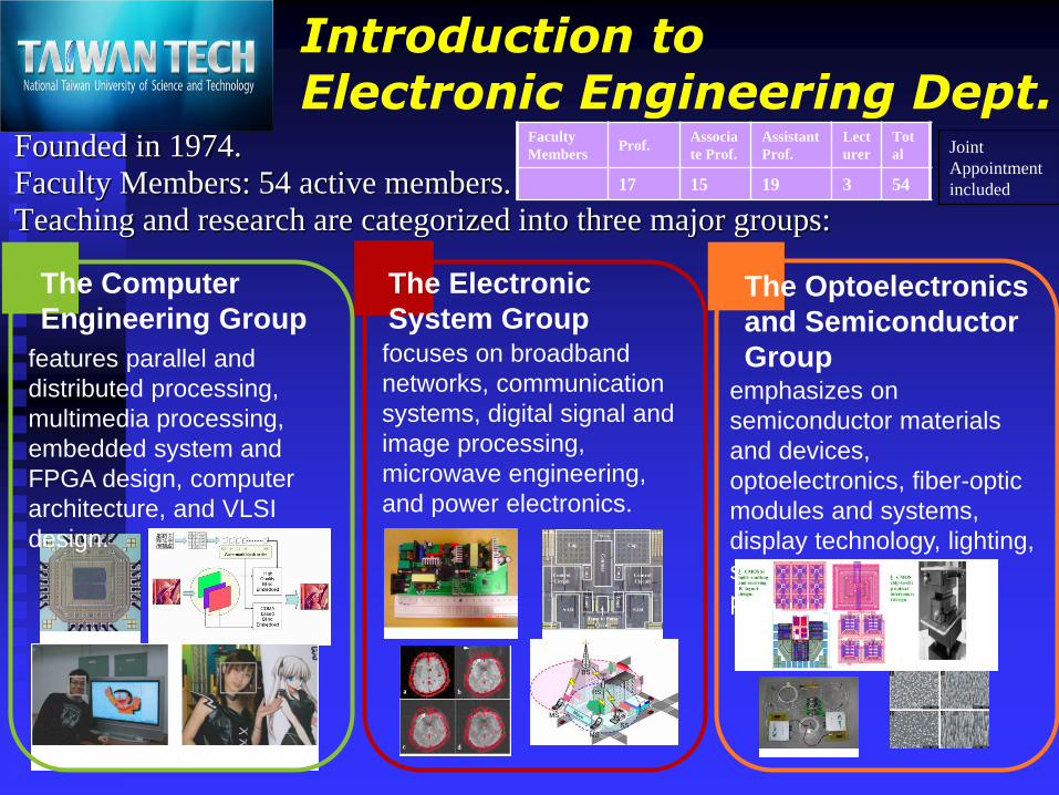
Introduction to Electronic Engineering Dept.
Founded in 1974.
Faculty Members: 54 active members.
Teaching and research are categorized into three major groups:
features parallel and
distributed processing,
multimedia processing,
embedded system and
FPGA design, computer
architecture, and VLSI
design.
The Computer
Engineering Group
The Electronic
System Group focuses on broadband
networks, communication
systems, digital signal and
image processing,
microwave engineering,
and power electronics.
The Optoelectronics
and Semiconductor
Group emphasizes on
semiconductor materials
and devices,
optoelectronics, fiber-optic
modules and systems,
display technology, lighting,
solar cells, and bio-
photonics.
Faculty
Members Prof.
Associa
te Prof.
Assistant
Prof.
Lect
urer
Tot
al
17 15 19 3 54
Joint
Appointment
included

Research Achievements of Electronic Engineering Dept.
Journal Paper Conference
Paper
Patent
2005 77 156 9
2006 117 148 8
2007 123 205 32
2008 156 185 31
Industry and Academia Cooperation ■To realize the advanced technologies for industrial applications.
■ The industry and academia cooperation is strongly encouraged.
■ The department seeks to build up strong links with the industry.
■ This elegantly balances the focus between theory and practice.
■ In the past few years, the department has achieved excellence in the
fields of embedded systems, IC chip design, wireless and
broadband networks, optical communications, image display, nano-
photonic materials and devices, bio-medical technologies and
solid-state lighting.
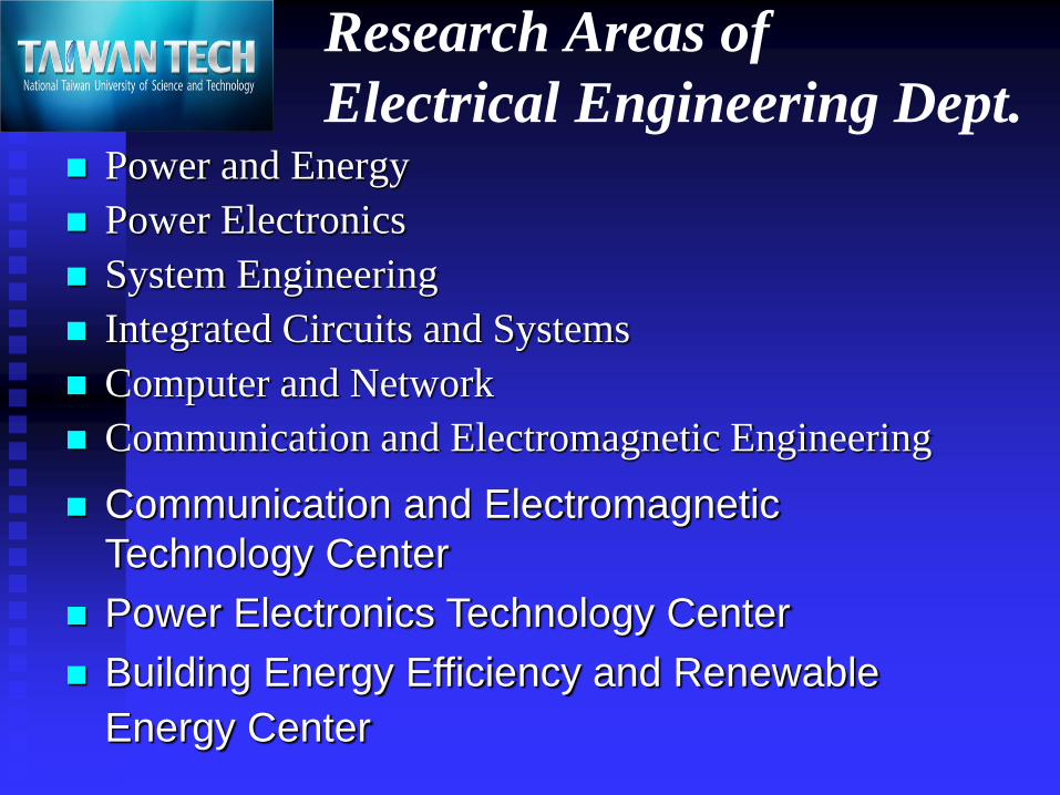
Research Areas of
Electrical Engineering Dept. Power and Energy
Power Electronics
System Engineering
Integrated Circuits and Systems
Computer and Network
Communication and Electromagnetic Engineering
Communication and Electromagnetic
Technology Center
Power Electronics Technology Center
Building Energy Efficiency and Renewable
Energy Center
Introduction to Computer Science and
Information Engineering Dept. (CSIE)
Founded in 1999
22 full-time faculty members:
Research in fields such as : (1) Multi-media Systems (2) Information security
(3) Artificial intelligence (4) Communication network
Research areas in Multi-media Systems include:
Image processing, video and data compression
Machine vision
Augmented reality
Voice synthesis, song synthesis, and related machine audio processing
Faculty
Members Prof.
Associ
ate
Prof.
Assistan
t Prof.
Lec
ture
r
Total
8 6 7 1 22
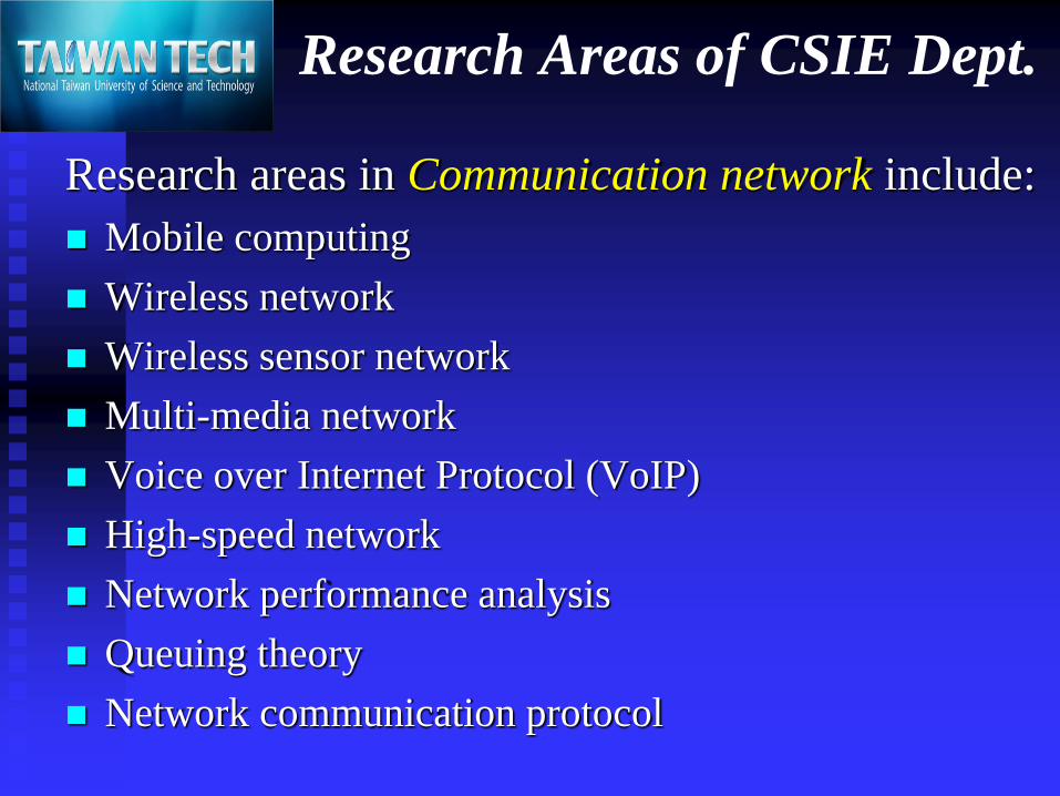
Research Areas of CSIE Dept.
Research areas in Communication network include:
Mobile computing
Wireless network
Wireless sensor network
Multi-media network
Voice over Internet Protocol (VoIP)
High-speed network
Network performance analysis
Queuing theory
Network communication protocol

Study Abroad Opportunities in Asia
Both are good schools and both should provide a good study abroad opportunity
If interested in either program contact:
Tatung University
Prof. Morris Chang (ISU coordinator) or
Prof. Randy Geiger
National Taiwan University of Science and Technology
Prof. Randy Geiger (ISU coordinator)
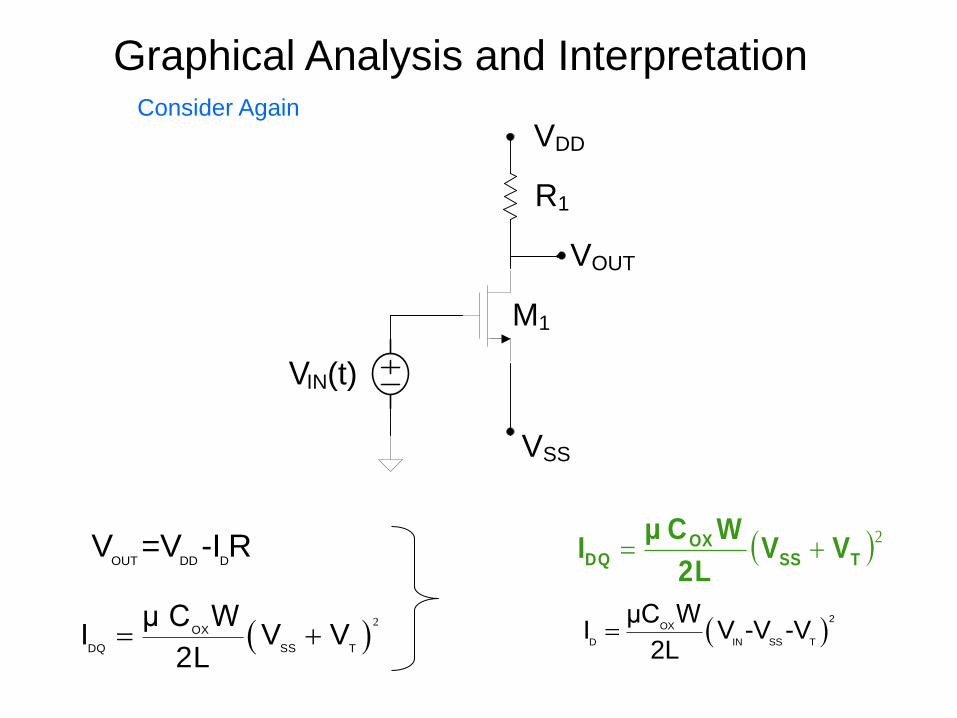
R1
VIN(t)
VOUT
VDD
VSS
M1
OUT DD DV =V -I R
2
OX
DQ SS T
μ C WI V V
2L
2OX
D IN SS T
μC WI V -V -V
2L
2
TSSOX
DQ VV2L
WC μI
Graphical Analysis and Interpretation Consider Again
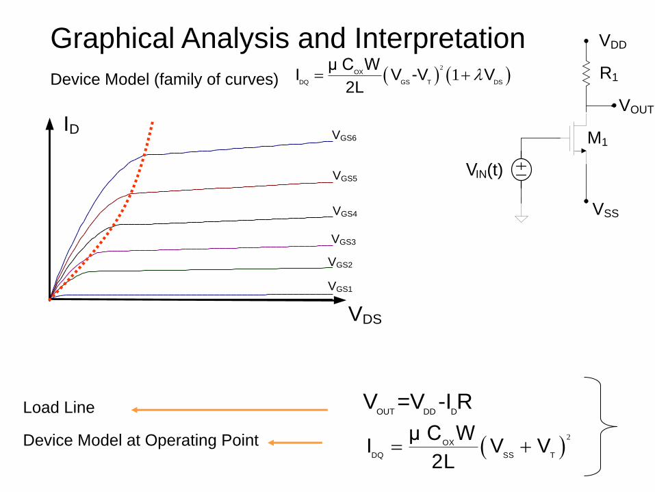
ID
VDS
VGS1
VGS6
VGS5
VGS4
VGS3
VGS2
R1
VIN(t)
VOUT
VDD
VSS
M1
OUT DD DV =V -I R
2
OX
DQ SS T
μ C WI V V
2L
Graphical Analysis and Interpretation
Device Model (family of curves) 2
1 OX
DQ GS T DS
μ C WI V -V V
2L
Load Line
Device Model at Operating Point
ID
VDS
VGS1
VGS6
VGS5
VGS4
VGS3
VGS2
Load LineQ-Point
R1
VIN(t)
VOUT
VDD
VSS
M1
OUT DD DV =V -I R
2
OX
DQ SS T
μ C WI V V
2L
2
OX
D IN SS T
μC WI V -V -V
2L
2
TSSOX
DQ VV2L
WC μI
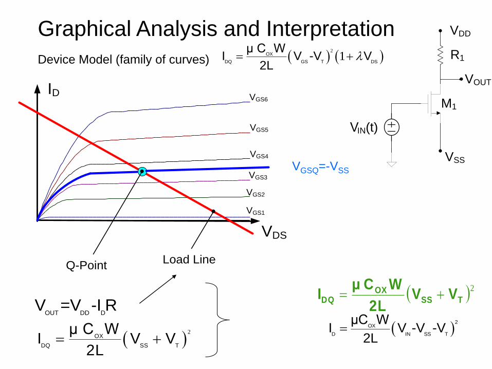
Graphical Analysis and Interpretation
VGSQ=-VSS
Device Model (family of curves) 2
1 OX
DQ GS T DS
μ C WI V -V V
2L
ID
VDS
VGS1
VGS6
VGS5
VGS4
VGS3
VGS2
Load LineQ-Point
R1
VIN(t)
VOUT
VDD
VSS
M1
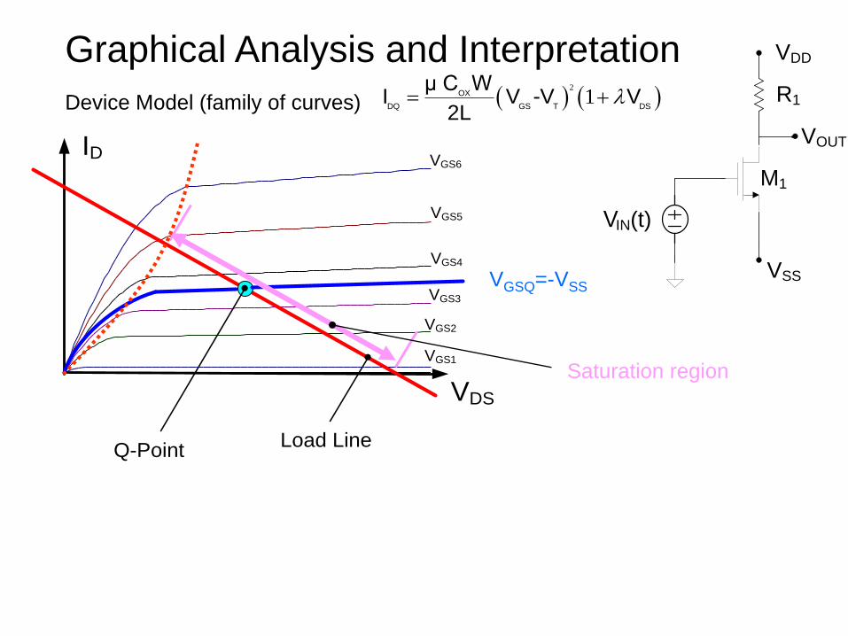
Graphical Analysis and Interpretation
VGSQ=-VSS
Device Model (family of curves) 2
1 OX
DQ GS T DS
μ C WI V -V V
2L
Saturation region
ID
VDS
VGS1
VGS6
VGS5
VGS4
VGS3
VGS2
Load LineQ-Point
R1
VIN(t)
VOUT
VDD
VSS
M1
Graphical Analysis and Interpretation
VGSQ=-VSS
Device Model (family of curves) 2
1 OX
DQ GS T DS
μ C WI V -V V
2L
Saturation region
• Linear signal swing region smaller than saturation region
• Modest nonlinear distortion provided saturation region operation maintained
• Symmetric swing about Q-point
• Signal swing can be maximized by judicious location of Q-point
ID
VDS
VGS1
VGS6
VGS5
VGS4
VGS3
VGS2
Load LineQ-Point
R1
VIN(t)
VOUT
VDD
VSS
M1
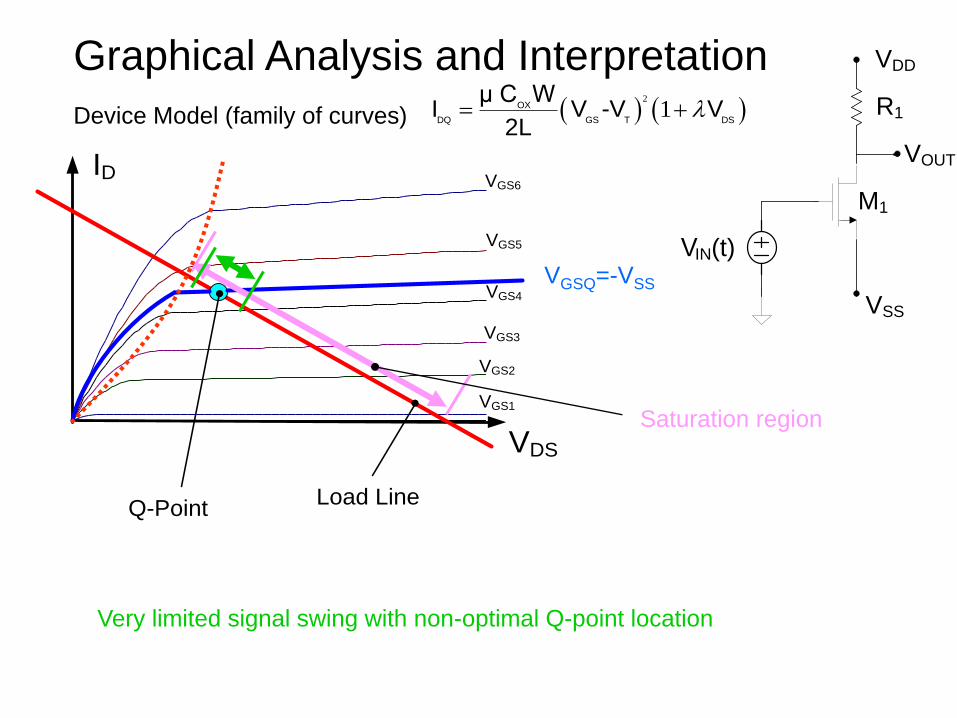
Graphical Analysis and Interpretation
VGSQ=-VSS
Device Model (family of curves) 2
1 OX
DQ GS T DS
μ C WI V -V V
2L
Saturation region
Very limited signal swing with non-optimal Q-point location
ID
VDS
VGS1
VGS6
VGS5
VGS4
VGS3
VGS2
Load LineQ-Point
R1
VIN(t)
VOUT
VDD
VSS
M1
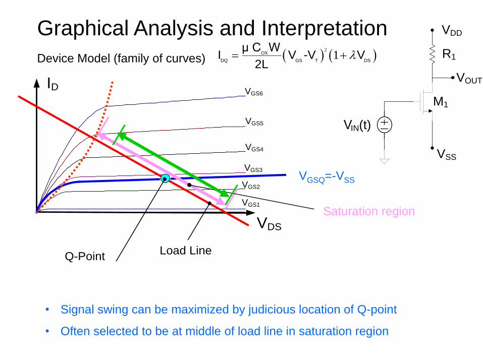
Graphical Analysis and Interpretation
VGSQ=-VSS
Device Model (family of curves) 2
1 OX
DQ GS T DS
μ C WI V -V V
2L
Saturation region
• Signal swing can be maximized by judicious location of Q-point
• Often selected to be at middle of load line in saturation region
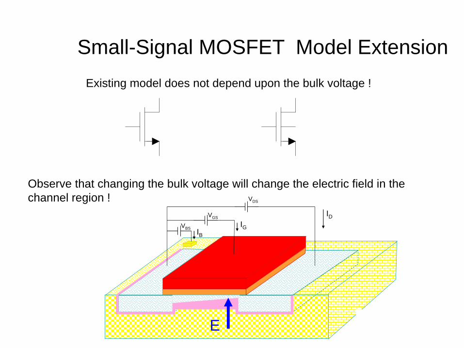
Small-Signal MOSFET Model Extension
Existing model does not depend upon the bulk voltage !
Observe that changing the bulk voltage will change the electric field in the
channel region !
VBS
VGS
VDS
IDIG
IB
(VBS small)
E
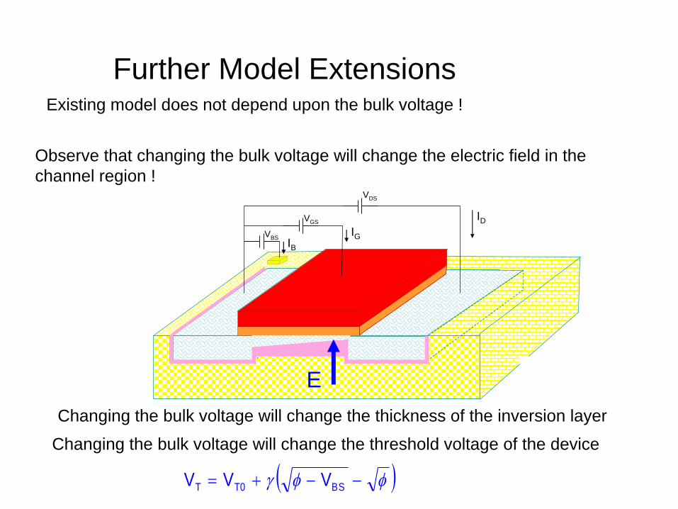
Further Model Extensions Existing model does not depend upon the bulk voltage !
Observe that changing the bulk voltage will change the electric field in the
channel region !
VBS
VGS
VDS
IDIG
IB
(VBS small)
E
Changing the bulk voltage will change the thickness of the inversion layer
Changing the bulk voltage will change the threshold voltage of the device
BST0T VVV

VT
VT0
VBS
~ -5V
BST0T VVV
Typical Effects of Bulk on Threshold Voltage for n-channel Device
1-20.4V 0.6V
Bulk-Diffusion Generally Reverse Biased (VBS< 0 or at least less than 0.3V) for n-
channel
Shift in threshold voltage with bulk voltage can be substantial
Often VBS=0
T T0 BSV V V
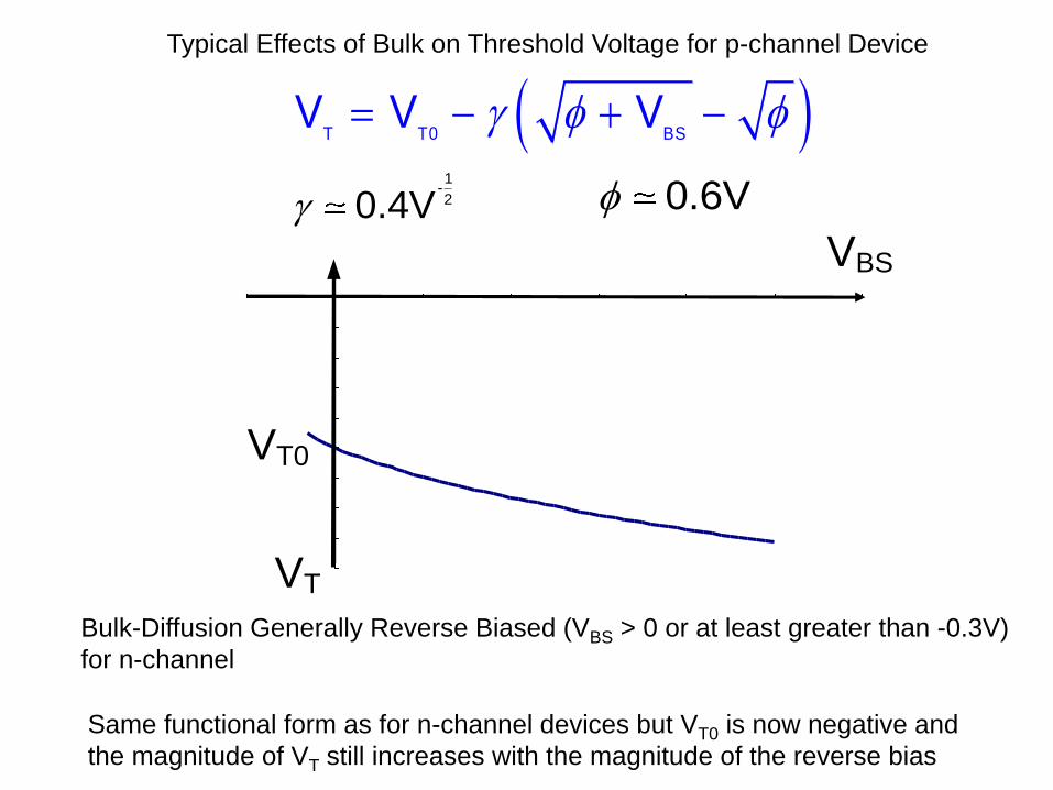
Typical Effects of Bulk on Threshold Voltage for p-channel Device
1-20.4V 0.6V
Bulk-Diffusion Generally Reverse Biased (VBS > 0 or at least greater than -0.3V)
for n-channel
VT
VT0
VBS
Same functional form as for n-channel devices but VT0 is now negative and
the magnitude of VT still increases with the magnitude of the reverse bias
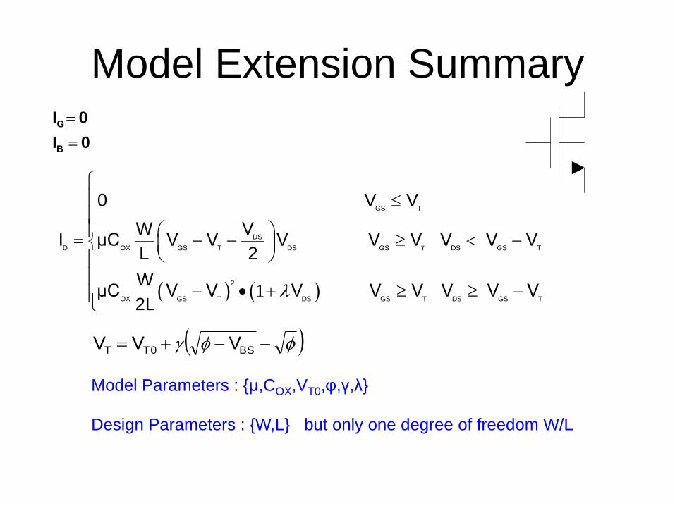
Model Extension Summary
1
GS T
DS
D OX GS T DS GS DS GS T
2
OX GS T DS GS T DS GS T
0 V V
VWI μC V V V V V V V V
L 2
WμC V V V V V V V V
2L
T
BST0T VVV
Model Parameters : {μ,COX,VT0,φ,γ,λ}
Design Parameters : {W,L} but only one degree of freedom W/L
0I
0I
B
G
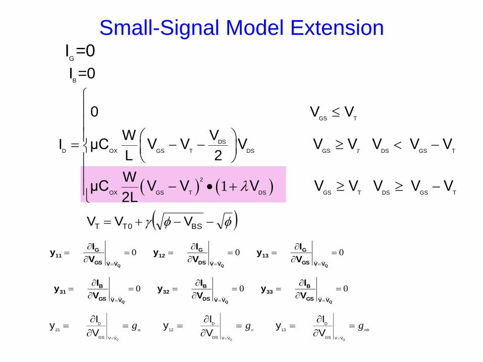
Small-Signal Model Extension
1
GS T
DS
D OX GS T DS GS DS GS T
2
OX GS T DS GS T DS GS T
0 V V
VWI μC V V V V V V V V
L 2
WμC V V V V V V V V
2L
T
BST0T VVV
000
QQQ VVGS
G13
VVDS
G12
VVGS
G11
V
Iy
V
Iy
V
Iy
000
QQQ VVGS
B33
VVDS
B32
VVGS
B31
V
Iy
V
Iy
V
Iy
Q Q Q
D D D
21 12 13
GS DS GSV V V V V V
I I Iy y y
V V Vm o mb
g g g
GI =0
BI =0

DS
2
TGSOXD VVV2L
WμCI 1
BST0T VVV
11
OX GS T DS OX EBQ
W WμC 2 V V V μC V
2L LQ
Q
D
m
V VGS V V
Ig
V
2
OX GS T DQ
WμC 2 V V λ λI
2LQ
Q
D
o
V VDS V V
Ig
V
1
OX GS T DS
WμC 2 V V 1+λV
2LQ Q
D T
mb
BS BSV V V V
I Vg
V V
1
21
1 12 Q
Q Q
D T
mb BS
V VBS BSV V V V
I Vg V
V V
OX EBQ OX EBQ
W WμC V μC V
L L
2m
BSQ
g-V
mbg
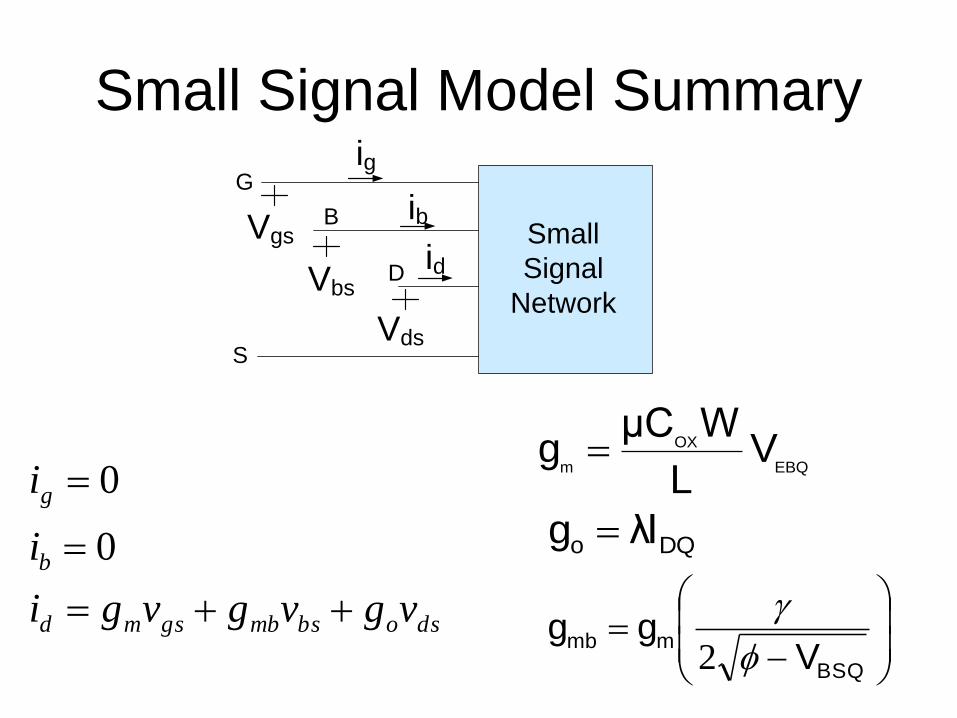
Small Signal Model Summary
OX
m EBQ
μC Wg V
L
DQo λIg
BSQ
mmbV
gg
2
G
S
Vgs
Vbs
Vds
id
ig
ibB
D
Small
Signal
Network
dsobsmbgsmd
b
g
vgvgvgi
i
i
0
0
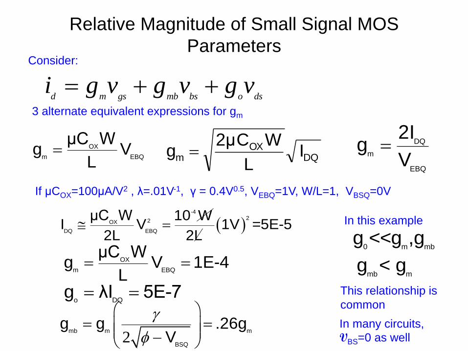
Relative Magnitude of Small Signal MOS
Parameters
OX
m EBQ
μC Wg V
L
o DQg λI 5E-7
2mb m m
BSQ
g g .26gV
d m gs mb bs o dsi g v g v g v
DQOX
m IL
WC2μg
DQ
m
EBQ
2Ig
V
Consider:
3 alternate equivalent expressions for gm
If μCOX=100μA/V2 , λ=.01V-1, γ = 0.4V0.5, VEBQ=1V, W/L=1, VBSQ=0V
-4
22OX
DQ EBQ
μC W 10 WI V 1V =5E-5
2L 2L
OX
m EBQ
μC Wg V 1E-4
L
0 m mbg <<g ,g
mb mg < g
In this example
This relationship is
common
In many circuits,
VBS=0 as well

Large and Small Signal Model Summary
dsobsmbgsmd
b
g
vgvgvgi
i
i
0
0
1
GS T
DS
D OX GS T DS GS DS GS T
2
OX GS T DS GS T DS GS T
0 V V
VWI μC V V V V V V V V
L 2
WμC V V V V V V V V
2L
T
BST0T VVV
Large Signal Model Small Signal Model
OX
m EBQ
μC Wg V
L
DQo λIg
BSQ
mmbV
gg
2
where
saturation
saturation
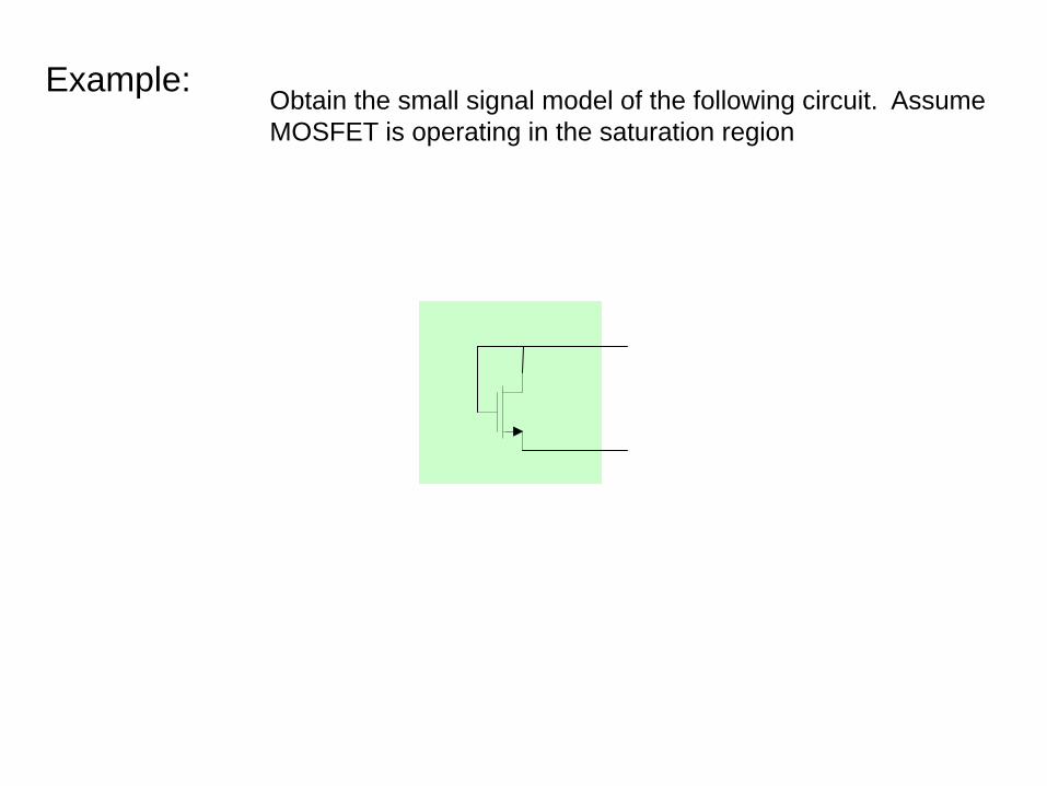
Example: Obtain the small signal model of the following circuit. Assume
MOSFET is operating in the saturation region

Example Obtain the small signal model of the following circuit. Assume
MOSFET is operating in the saturation region
Solution:
gmvgsvgsg0
G D
V
I
0mV g g I
0
1 1EQ
m m
Rg g g
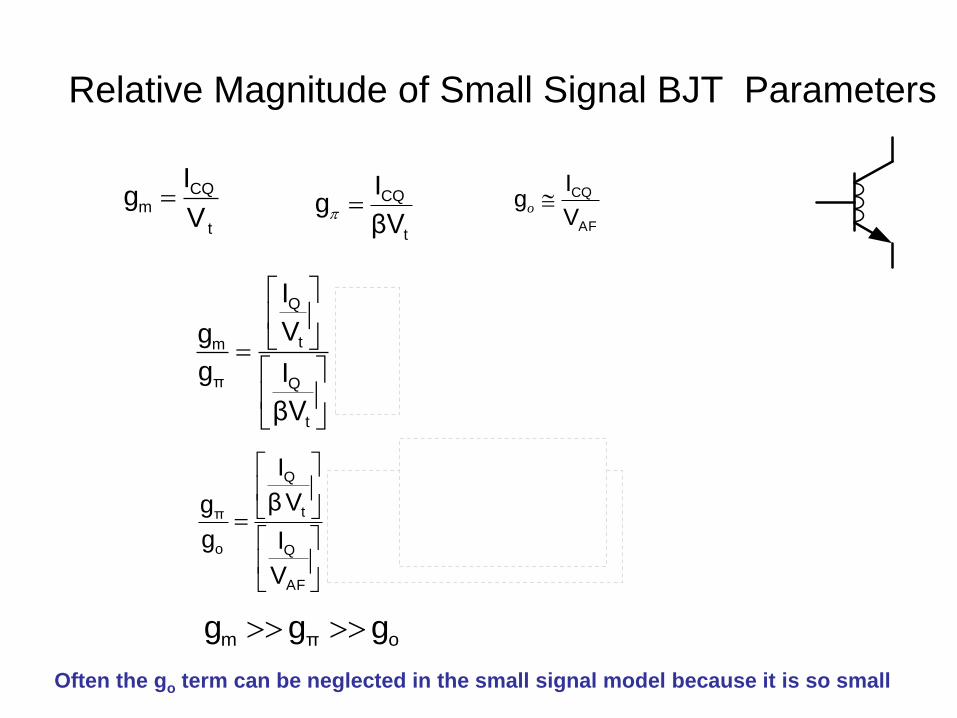
Relative Magnitude of Small Signal BJT Parameters
t
CQm
V
Ig
t
CQ
βV
Ig
AF
CQ
V
Ig o
β
βV
I
V
I
g
g
t
Q
t
Q
π
m
7726mV100
200V
Vβ
V
V
I
Vβ
I
g
g
t
AF
AF
Q
t
Q
o
π
oπm ggg
Often the go term can be neglected in the small signal model because it is so small
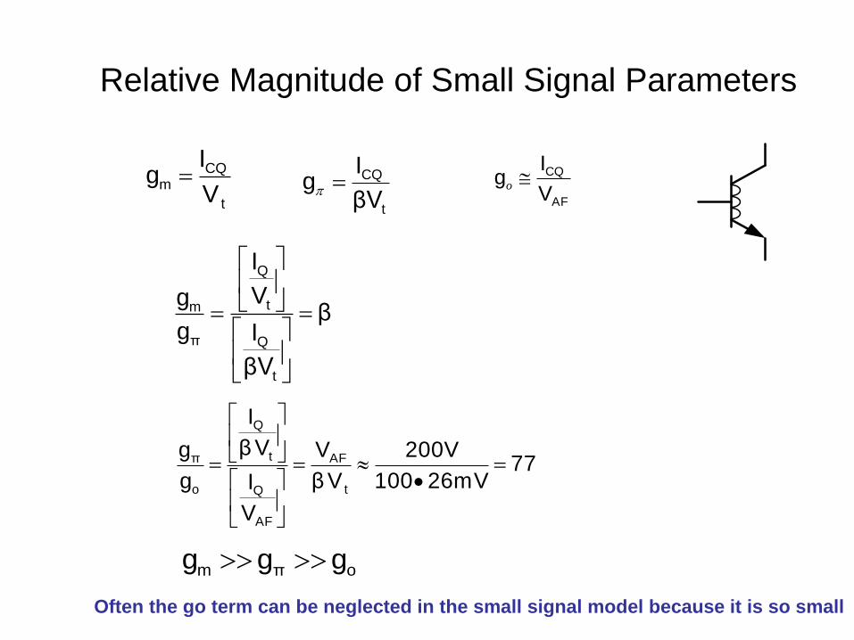
Relative Magnitude of Small Signal Parameters
t
CQm
V
Ig
t
CQ
βV
Ig
AF
CQ
V
Ig o
β
βV
I
V
I
g
g
t
Q
t
Q
π
m
7726mV100
200V
Vβ
V
V
I
Vβ
I
g
g
t
AF
AF
Q
t
Q
o
π
oπm ggg
Often the go term can be neglected in the small signal model because it is so small

End of Lecture 28