Embed Size (px)
Citation preview
Applied Power Electronics
Bachelor of Technology
VIIth Semester
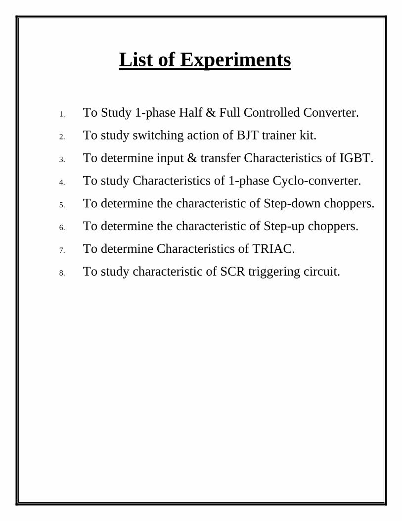
List of Experiments
1.
2.
3.
4.
5.
6.
7.
8.
To Study 1-phase Half & Full Controlled Converter.
To study switching action of BJT trainer kit.
To determine input & transfer Characteristics of IGBT.
To study Characteristics of 1-phase Cyclo-converter.
To determine the characteristic of Step-down choppers.
To determine the characteristic of Step-up choppers.
To determine Characteristics of TRIAC.
To study characteristic of SCR triggering circuit.
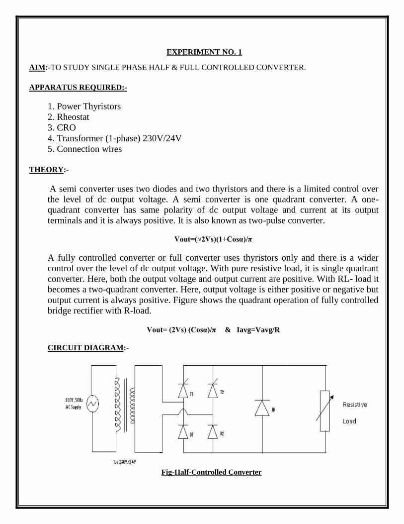
EXPERIMENT NO. 1
AIM:-TO STUDY SINGLE PHASE HALF & FULL CONTROLLED CONVERTER.
APPARATUS REQUIRED:-
1. Power Thyristors
2. Rheostat 3. CRO
4. Transformer (1-phase) 230V/24V
5. Connection wires
THEORY:-
A semi converter uses two diodes and two thyristors and there is a limited control over the level of dc output voltage. A semi converter is one quadrant converter. A one-
quadrant converter has same polarity of dc output voltage and current at its output terminals and it is always positive. It is also known as two-pulse converter.
Vout=(√2Vs)(1+Cosα)/π
A fully controlled converter or full converter uses thyristors only and there is a wider
control over the level of dc output voltage. With pure resistive load, it is single quadrant
converter. Here, both the output voltage and output current are positive. With RL- load it
becomes a two-quadrant converter. Here, output voltage is either positive or negative but
output current is always positive. Figure shows the quadrant operation of fully controlled
bridge rectifier with R-load.
Vout= (2Vs) (Cosα)/π & Iavg=Vavg/R
CIRCUIT DIAGRAM:-
Fig-Half-Controlled Converter
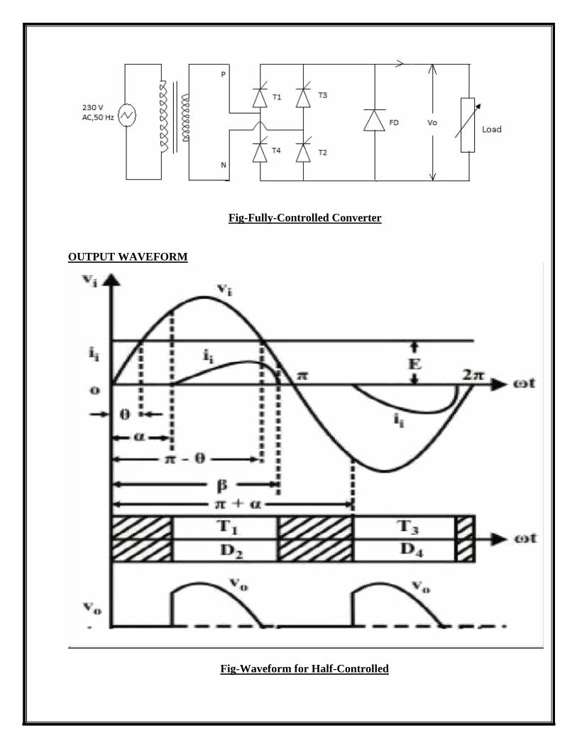
Fig-Fully-Controlled Converter
OUTPUT WAVEFORM
Fig-Waveform for Half-Controlled
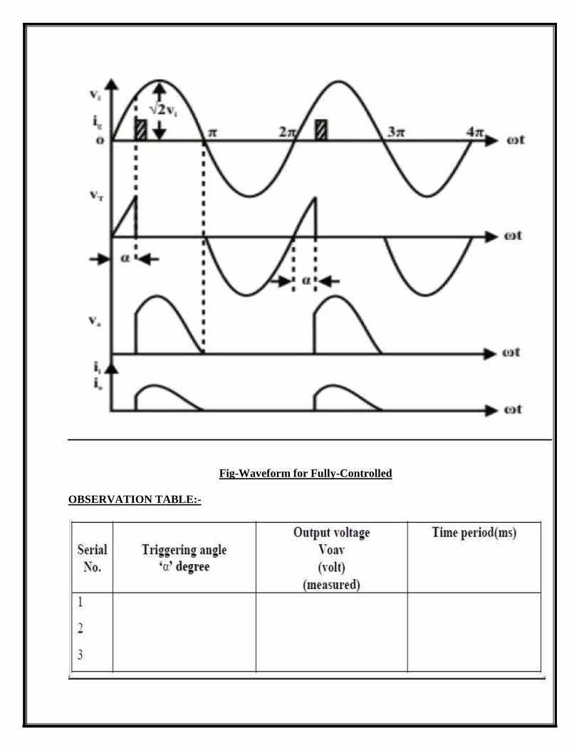
Fig-Waveform for Fully-Controlled
OBSERVATION TABLE:-

PROCEDURE:-
Procedure for Half-Controlled:
1. Make the connections as per the circuit diagram.
2. Connect CRO and voltmeter across the load.
3. Keep the potentiometer at the minimum position. 4. Switch on the step down ac source.
5. Check the gate pulses at G1-K1 & G2-K2, respectively.
6. Observe the wave form on CRO and note the triggering angle „α‟ and 7. Note the corresponding reading of the voltmeter. Also note the value of Maximum amplitude Vm from the waveform. 8. Set the potentiometer at different positions and follow the step given in (6) for every position. 9. Tabulate the readings in the observation column.
Procedure for Fully-Controlled:
1. Single Phase Fully Controlled Bridge Rectifier
2. Make the connections as per the circuit diagram. 3. Connect CRO and multimeter (in dc) across the load. 4. Keep the potentiometer (Ramp control) at the minimum position (maximum resistance). 5. Switch on the step down ac source.
6. Check the gate pulses at G1-K1, G2-K2,G3-K3,& G4-K4 respectively. 7. Observe the waveform on CRO and note the triggering angle „α‟ and note the corresponding reading of the multimeter. Also note the value of maximum amplitude
Vm from the waveform. 8. Set the potentiometer at different positions and follow the step given in (6) for every position. 9. Tabulate the readings in observation column.
10. Draw the waveforms observed on CRO.
PRECAUCATION:-
1. Follow the entire recommended dimension.
2. Properly connect all the equipment.
3. Check the insulation between the probes.
4. Shoes must be part of attire while doing the lab. 5. Before giving the supply check all the connections once again.

RESULT:-
Thus the operation of single phase half controlled converter using R and RL load has been studied and the output waveforms has been observed.
Thus the operation of single phase fully controlled converter using R and RL load has been studied and the output waveforms has been observed.
EXPERIMENT NO. 2
AIM:-TO STUDY THE SWITCHING ACTION OF BJT TRAINER KIT.
APPARATUS REQUIRED:-
1. BJT Trainer Kit
2. Multimeter 3. Connecting Leads
THEORY:-
Power Bipolar Junction Transistor (BJT) is the first semiconductor device to allow full
control over its Turn on and Turn off operations. It simplified the design of a large
number of Power Electronic circuits that used forced commutated thyristors at that time
and also helped realize a number of new circuits. Subsequently, many other devices that
can broadly be classified as “Transistors” have been developed. Many of them have
superior performance compared to the BJT in some respects. They have, by now, almost
completely replaced BJTs. However, it should be emphasized that the BJT was the first
semiconductor device to closely approximate an ideal fully controlled Power switch.
Other “transistors” have characteristics that are qualitatively similar to those of the BJT
(although the physics of operation may differ). Hence, it will be worthwhile studying the
characteristics and operation a BJT in some depth. From the point of view of
construction and operation BJT is a bipolar (i.e. minority carrier) current controlled
device. It has been used at signal level power for a long time. However, the construction
and operating characteristics of a Power BJT differs significantly from its signal level
counterpart due to the requirement for a large blocking voltage in the “OFF” state and a
high current carrying capacity in the “ON” state.
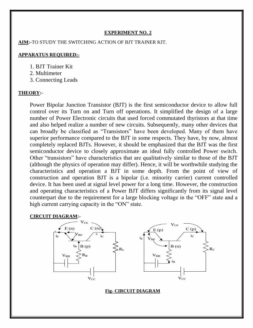
CIRCUIT DIAGRAM:-
Fig- CIRCUIT DIAGRAM

CHARACTERISTIC:-
Fig- CHARACTERISTC OF BJT CIRCUIT
PROCEDURE:-
1. Connect the circuit as shown in connection diagram. 2. As voltage near about (0.6-0.7) i.e, VBE or greater then transistor conducts and due to base current collector current appears. 3. And when transistor conducts then switching of Relay also takes place i.e, NC to NO and DC Motor starts rotating.
4. Ammeter is internally connected between relay and collector.
5. As we vary Vin then due to this, collector current is show in the analog ammeter.
PRECAUCATION:-
1. Follow the entire recommended dimension.
2. Properly connect all the equipment.

3. Check the insulation between the probes.
4. Shoes must be part of attire while doing the lab. 5. Before giving the supply check all the connections once again.
RESULT:-
Studied the switching action of BJT Tainer Kit.
EXPERIMENT NO. 3
AIM:-TO DETERMINE INPUT & TRANSFER CHARACTERISTICS OF IGBT
APPARATUS REQUIRED:-
1. IGBT Trainer Kit
2. Multimeter 3. Connecting Leads
THEORY:-
An insulated-gate bipolar transistor (IGBT) is a three-terminal power semiconductor
device primarily used as an electronic switch which, as it was developed, came to combine
high efficiency and fast switching. It switches electric power in many modern appliances:
variable-frequency drives (VFDs), electric cars, trains, variable speed refrigerators, lamp
ballasts, air-conditioners and even stereo systems with switching amplifiers. Since it is
designed to turn on and off rapidly, amplifiers that use it often synthesize complex waveforms
with pulse-width modulation and low-pass filters. In switching applications modern devices
feature pulse repetition rates well into the ultrasonic range—frequencies which are at least ten
times the highest audio frequency handled by the device when used as an analog audio
amplifier.
The IGBT combines the simple gate-drive
characteristics of MOSFETs with the high-current and low-saturation-voltage capability of
bipolar transistors. The IGBT combines an isolated-gate FET for the control input and a
bipolar power transistor as a switch in a single device. The IGBT is used in medium- to high-
power applications like switched-mode power supplies, traction motor control and induction
heating.
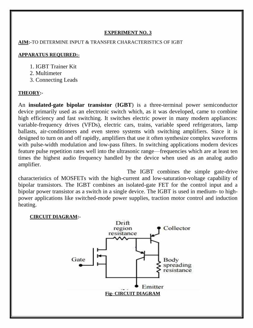
CIRCUIT DIAGRAM:-
Fig- CIRCUIT DIAGRAM
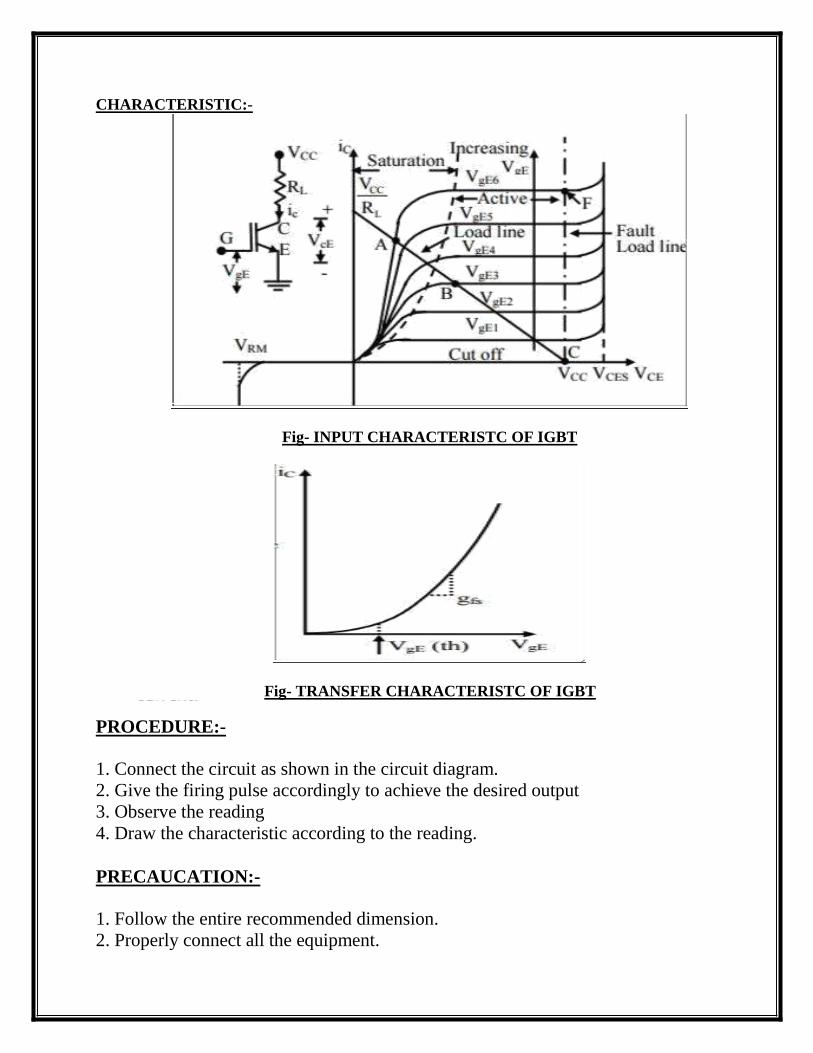
CHARACTERISTIC:-
Fig- INPUT CHARACTERISTC OF IGBT
Fig- TRANSFER CHARACTERISTC OF IGBT
PROCEDURE:-
1. Connect the circuit as shown in the circuit diagram.
2. Give the firing pulse accordingly to achieve the desired output
3. Observe the reading 4. Draw the characteristic according to the reading.
PRECAUCATION:-
1. Follow the entire recommended dimension.
2. Properly connect all the equipment.

3. Check the insulation between the probes.
4. Shoes must be part of attire while doing the lab. 5. Before giving the supply check all the connections once again.
RESULT:-
Studied the Input and Transfer characteristics of IGBT.

EXPERIMENT NO. 4
AIM:-TO STUDY CHARACTERISTICS OF SINGLE-PHASE CYCLOCONVERTER
APPARATUS REQUIRED:-
1. Power Electronics Trainer Kit
2. Firing Circuit 3. CRO
THEORY:-
Cyclo converter is a circuit which converts the input voltage at one frequency to the Output voltage at different frequecy.
During the positive half cycle Thyristors P1, N2 are forward biased and Thyristors P2 and N1 are reverse biased. The circuit is designed for step down cyclo converter for a output frequency of = 3 .To get the desired frequency the Thyristors are triggered accordingly.
During the first positive half cycle P1 and N2 are forward biased and to get the positive
output voltage, P1 is triggered at an angle of (π+α). During the next positive half cycle
P2 and N1 are forward biased, to get required output voltage thyristor P2 is triggered. In
the next half cycle P1 is triggered next N1, N2 and again N1 are triggered accordingly.
This process repeats.
CIRCUIT DIAGRAM:-
Fig-Single-Phase Step-Down Cyclo-Converter

OUTPUT WAVEFORM
Fig-Waveform for Single-Phase Step-Down Cyclo-Converter

PROCEDURE:-
1. Connect the circuit as shown in the circuit diagram. 2. Give the firing pulses accordingly at a suitable firing angle from the firing circuit. 3. Observe the load voltage on the CRO and note down the firing angle.
PRECAUCATION:-
1. Follow the entire recommended dimension.
2. Properly connect all the equipment.
3. Check the insulation between the probes. 4. Shoes must be part of attire while doing the lab.
5. Before giving the supply check all the connections once again.
RESULT:-
Thus the operation of single phase Cyclo-converter using R load has studied and the output waveforms has been observed.
EXPERIMENT NO. 5
AIM:-TO DETERMINE THE CHARACTERISTIC OF STEP-DOWN CHOPPER (BUCK CONVETER).
SOFTWARE USED:-
MATLAB
THEORY:-
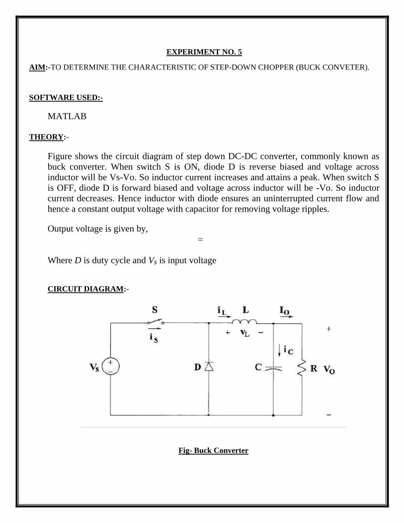
Figure shows the circuit diagram of step down DC-DC converter, commonly known as
buck converter. When switch S is ON, diode D is reverse biased and voltage across
inductor will be Vs-Vo. So inductor current increases and attains a peak. When switch S
is OFF, diode D is forward biased and voltage across inductor will be -Vo. So inductor
current decreases. Hence inductor with diode ensures an uninterrupted current flow and
hence a constant output voltage with capacitor for removing voltage ripples.
Output voltage is given by,
=
Where D is duty cycle and Vs is input voltage
CIRCUIT DIAGRAM:-
Fig- Buck Converter
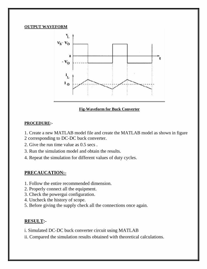
OUTPUT WAVEFORM
Fig-Waveform for Buck Converter
PROCEDURE:-
1. Create a new MATLAB model file and create the MATLAB model as shown in figure
2 corresponding to DC-DC buck converter. 2. Give the run time value as 0.5 secs . 3. Run the simulation model and obtain the results. 4. Repeat the simulation for different values of duty cycles.
PRECAUCATION:-
1. Follow the entire recommended dimension.
2. Properly connect all the equipment.
3. Check the powergui configuration. 4. Uncheck the history of scope.
5. Before giving the supply check all the connections once again.
RESULT:-
i. Simulated DC-DC buck converter circuit using MATLAB
ii. Compared the simulation results obtained with theoretical calculations.

EXPERIMENT NO. 6
AIM:-TO DETERMINE THE CHARACTERISTIC OF STEP-UP CHOPPER (BOOST CONVETER).
SOFTWARE USED:-
MATLAB
THEORY:-
The key principle that drives the boost converter is the tendency of an inductor to resist changes in current by creating and destroying a magnetic field. In a boost converter, the output voltage is always higher than the input voltage. A schematic of a boost power
stage is shown in below Figure.
(a) When the switch is closed, current flows through the inductor in clockwise direction and the inductor stores some energy by generating a magnetic field. Polarity of the left side of the inductor is positive.
(b) When the switch is opened, current will be reduced as the impedance is higher. The magnetic field previously created will be destroyed to maintain the current towards the
load. Thus the polarity will be reversed (means left side of inductor will be negative now). As a result, two sources will be in series causing a higher voltage to charge the
capacitor through the diode D.
Output voltage is given by, =
Where D is duty cycle and Vs is input voltage
CIRCUIT DIAGRAM:-
Fig- Boost Converter
OUTPUT WAVEFORM
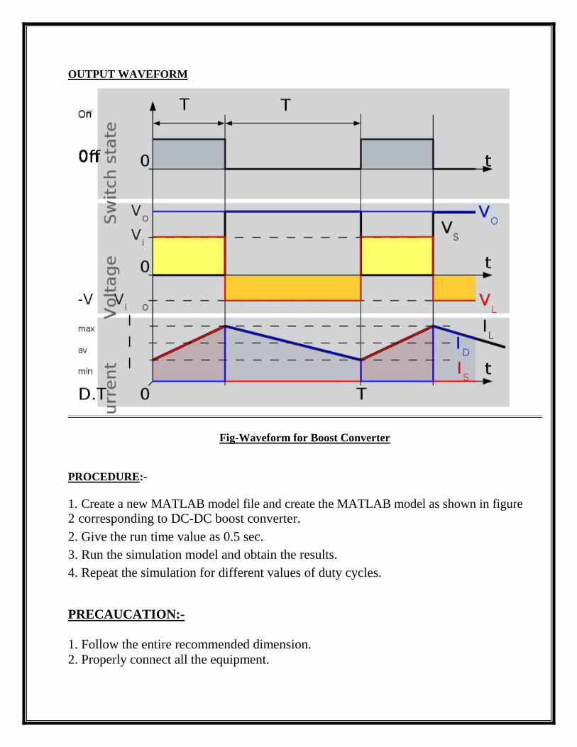
Fig-Waveform for Boost Converter
PROCEDURE:-
1. Create a new MATLAB model file and create the MATLAB model as shown in figure
2 corresponding to DC-DC boost converter. 2. Give the run time value as 0.5 sec. 3. Run the simulation model and obtain the results. 4. Repeat the simulation for different values of duty cycles.
PRECAUCATION:-
1. Follow the entire recommended dimension.
2. Properly connect all the equipment.

3. Check the powergui configuration.
4. Uncheck the history of scope.
5. Before giving the supply check all the connections once again.
RESULT:-
i. Simulated DC-DC boost converter circuit using MATLAB
ii. Compared the simulation results obtained with theoretical calculations.
EXPERIMENT NO. 7
AIM:-TO DETERMINE THE CHARACTERISTIC OF TRIAC.
APPARATUS REQUIRED:-
1. TRIAC Kit
2. Multimeter 3. Connecting Leads
THEORY:-
The TRIAC is a three-terminal ac switch that is triggered into conduction when a low-
energy signal is applied to its gate terminal. Unlike the SCR, the TRIAC conducts in either direction when turned on. The TRIAC also differs from the SCR in that either a
positive or negative gate signal triggers it into conduction. Thus the TRIAC is a three terminal, four layer bidirectional semiconductor device that controls ac power whereas
an SCR controls dc power or forward biased half cycles of ac in a load. Because of its bidirectional conduction property, the TRIAC is widely used in the field of power
electronics for control purposes.
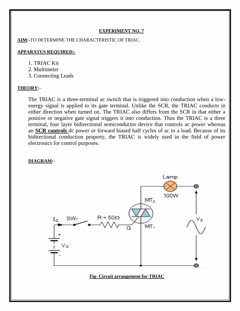
DIAGRAM:-
Fig- Circuit arrangement for TRIAC
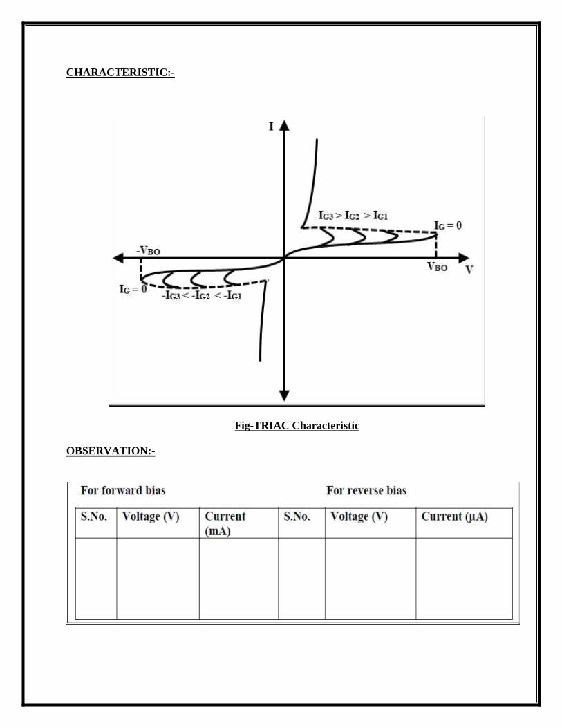
CHARACTERISTIC:-
Fig-TRIAC Characteristic
OBSERVATION:-

PROCEDURE:-
PRECAUCATION:-
1. Follow the entire recommended dimension.
2. Properly connect all the equipment.
3. Check the powergui configuration.
4. Uncheck the history of scope.
5. Before giving the supply check all the connections once again.
RESULT:-
The V-I characteristics of TRIAC is plotted on the graph which is true according to theory.
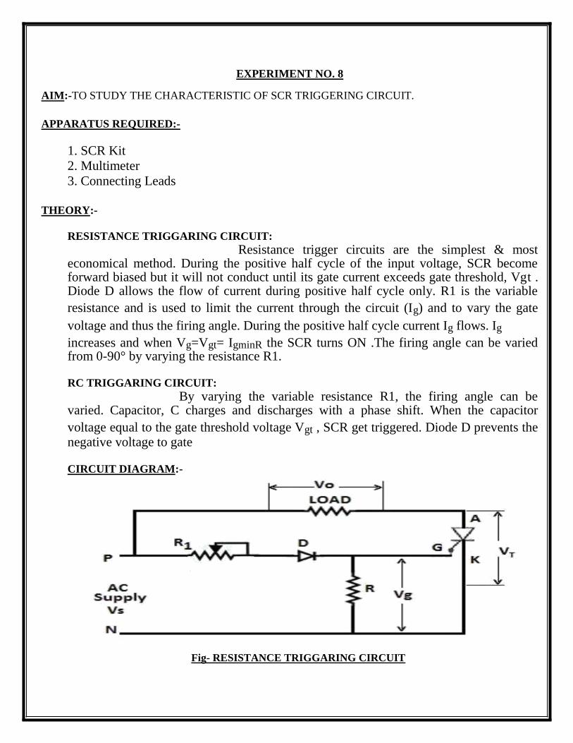
EXPERIMENT NO. 8
AIM:-TO STUDY THE CHARACTERISTIC OF SCR TRIGGERING CIRCUIT.
APPARATUS REQUIRED:-
1. SCR Kit
2. Multimeter 3. Connecting Leads
THEORY:-
RESISTANCE TRIGGARING CIRCUIT:
Resistance trigger circuits are the simplest & most economical method. During the positive half cycle of the input voltage, SCR become forward biased but it will not conduct until its gate current exceeds gate threshold, Vgt . Diode D allows the flow of current during positive half cycle only. R1 is the variable
resistance and is used to limit the current through the circuit (Ig) and to vary the gate
voltage and thus the firing angle. During the positive half cycle current Ig flows. Ig
increases and when Vg=Vgt= IgminR the SCR turns ON .The firing angle can be varied from 0-90° by varying the resistance R1.
RC TRIGGARING CIRCUIT:
By varying the variable resistance R1, the firing angle can be varied. Capacitor, C charges and discharges with a phase shift. When the capacitor
voltage equal to the gate threshold voltage Vgt , SCR get triggered. Diode D prevents the negative voltage to gate
CIRCUIT DIAGRAM:-
Fig- RESISTANCE TRIGGARING CIRCUIT
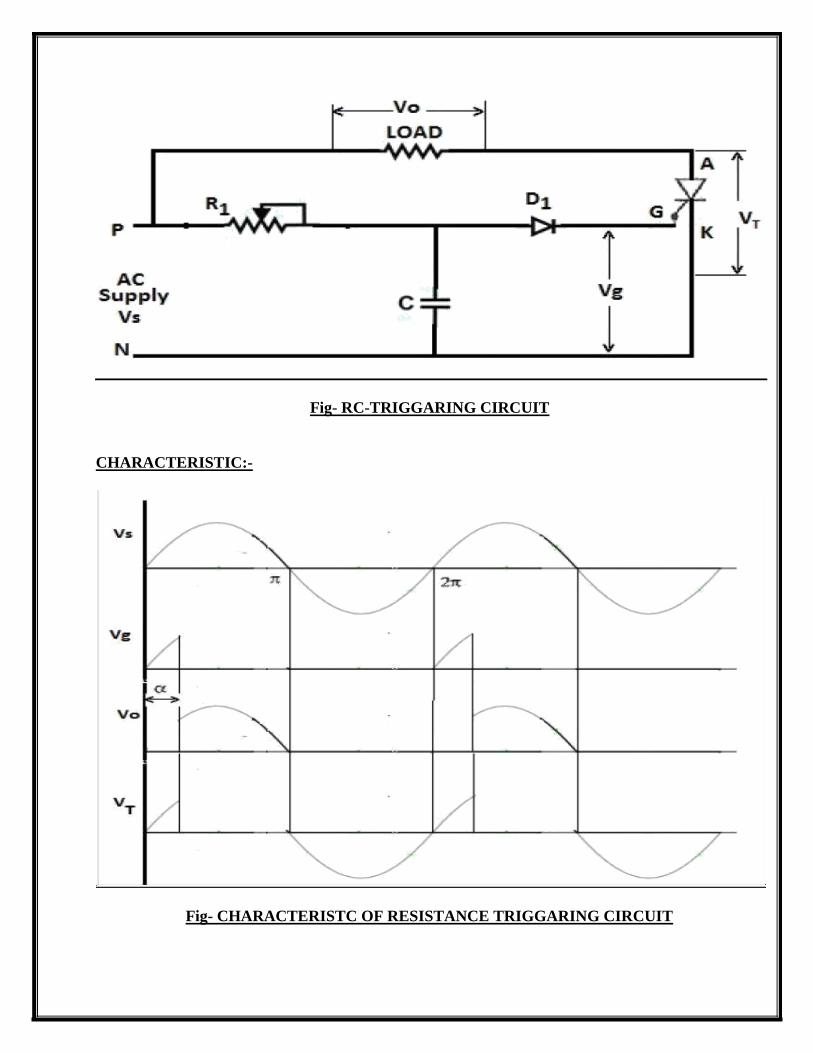
Fig- RC-TRIGGARING CIRCUIT
CHARACTERISTIC:-
Fig- CHARACTERISTC OF RESISTANCE TRIGGARING CIRCUIT
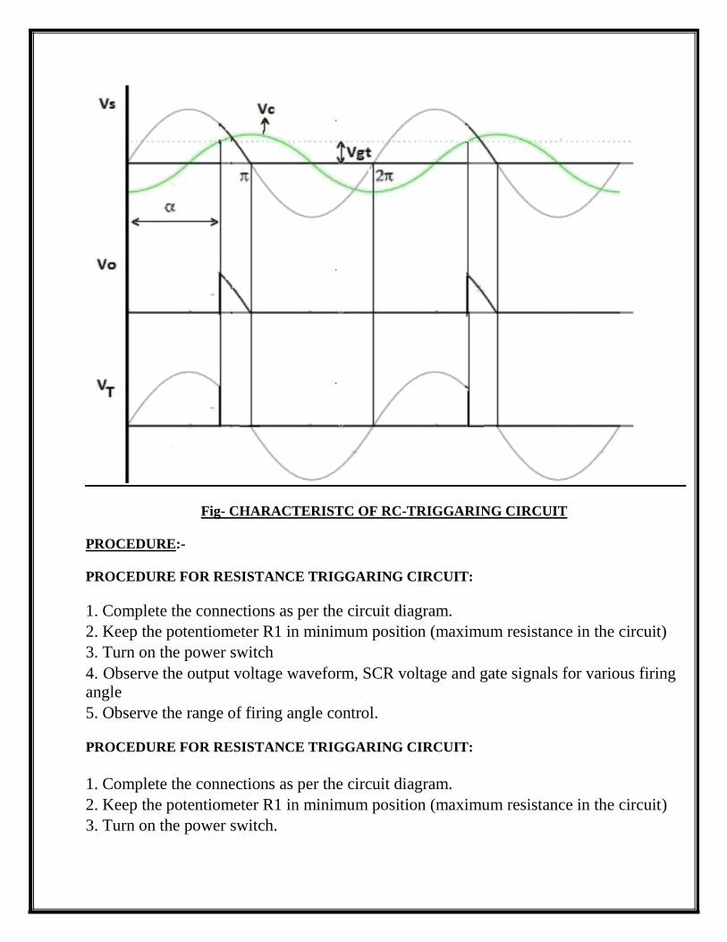
Fig- CHARACTERISTC OF RC-TRIGGARING CIRCUIT
PROCEDURE:-
PROCEDURE FOR RESISTANCE TRIGGARING CIRCUIT:
1. Complete the connections as per the circuit diagram. 2. Keep the potentiometer R1 in minimum position (maximum resistance in the circuit) 3. Turn on the power switch 4. Observe the output voltage waveform, SCR voltage and gate signals for various firing angle 5. Observe the range of firing angle control.
PROCEDURE FOR RESISTANCE TRIGGARING CIRCUIT:
1. Complete the connections as per the circuit diagram. 2. Keep the potentiometer R1 in minimum position (maximum resistance in the circuit) 3. Turn on the power switch.

4. Observe the output voltage waveform, SCR voltage and gate signals for various firing angle 5. Observe the range of firing angle control.
PRECAUCATION:-
1. Follow the entire recommended dimension. 2. Properly connect all the equipment.
3. Check the insulation between the probes.
4. Shoes must be part of attire while doing the lab.
5. Before giving the supply check all the connections once again.
RESULT:-
Studied the operation of R and RC Triggering circuit for SCR for different firing angles.