Embed Size (px)
DESCRIPTION
Design apps software.
Citation preview
SWRU137B 1
CC2520 Software Examples
User’s Guide
SWRU137B 2
Table of contents
1 Introduction................................................................................................................................................... 3
2 Abbreviations ................................................................................................................................................ 3
3 Using the software......................................................................................................................................... 4 3.1 Prerequisites ........................................................................................................................................... 4 3.2 Getting started......................................................................................................................................... 5
3.2.1 Set up Hardware and Software........................................................................................................ 5 3.2.2 Program the board with IAR ........................................................................................................... 5 3.2.3 Peripherals used by the example code............................................................................................. 6 3.2.4 Configuring HyperTerminal............................................................................................................ 6
4 Application Examples ................................................................................................................................... 8 4.1 Hello application..................................................................................................................................... 9 4.2 Register read application........................................................................................................................ 9 4.3 Light/Switch application ....................................................................................................................... 10 4.4 Packet Error Rate tester application..................................................................................................... 12 4.5 Spectrum Analyzer application ............................................................................................................. 13 4.6 CCM Security application..................................................................................................................... 13
5 Software Library Reference....................................................................................................................... 15 5.1 Software architecture ............................................................................................................................ 15
5.1.1 Software folder structure............................................................................................................... 15 5.2 Basic RF................................................................................................................................................ 16
5.2.1 Basic RF frame format .................................................................................................................. 16 5.2.2 Basic RF usage instructions .......................................................................................................... 17 5.2.3 Basic RF API reference................................................................................................................. 18 5.2.4 Basic RF operation........................................................................................................................ 19 5.2.5 Limitations of Basic RF ................................................................................................................ 24
5.3 Hardware Abstraction Layer ................................................................................................................ 25 5.3.1 HAL RF API reference ................................................................................................................. 25
References............................................................................................................................................................ 27
Document History ............................................................................................................................................... 27
SWRU137B 3
1 Introduction This document describes software examples for the CC2520 IEEE 802.15.4 compliant RF transceiver. It also describes the necessary hardware and software to run the examples, and how to get started. A comprehensive description of the hardware in the CC2520DK is found in the CC2520 Development Kit User’s Guide. There is also a CC2520DK Quick Start Guide which gives a short tutorial on how to get started with the kit. These documents are found on the CC2520DK website [3]. These software examples also apply to apply when the CC2520 is used with the CC2591. Section 3 of this document describes necessary prerequisites and how to get started with the code examples. Section 4 describes how to run each of the application examples. The software library that the code examples are built upon is described in section 5. The latter section also gives an API reference and describes the functionality of the software library.
2 Abbreviations API - Application Programming Interface CCM - Counter with CBC-MAC (mode of operation) CCM* - Extension of CCM FCS - Frame Check Sequence HAL - Hardware Abstraction Layer IO - Input/Output MIC - Message Integrity Code MPDU - MAC Protocol Data Unit PAN - Personal Area Network PER - Packet Error Rate RF - Radio Frequency RSSI - Received Signal Strength Indicator
SWRU137B 4
3 Using the software This section describes the necessary hardware and software, and how to get started with the application examples for CC2520.
3.1 Prerequisites To successfully download and run the software described in this document, the following material is needed:
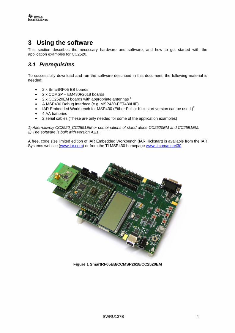
• 2 x SmartRF05 EB boards • 2 x CCMSP – EM430F2618 boards • 2 x CC2520EM boards with appropriate antennas 1 • A MSP430 Debug Interface (e.g. MSP430-FET430UIF) • IAR Embedded Workbench for MSP430 (Either Full or Kick start version can be used )2 • 4 AA batteries • 2 serial cables (These are only needed for some of the application examples)
1) Alternatively CC2520_CC2591EM or combinations of stand-alone CC2520EM and CC2591EM. 2) The software is built with version 4.21.. A free, code size limited edition of IAR Embedded Workbench (IAR Kickstart) is available from the IAR Systems website (www.iar.com) or from the TI MSP430 homepage www.ti.com/msp430.
Figure 1 SmartRF05EB/CCMSP2618/CC2520EM
SWRU137B 5
3.2 Getting started The following sections describe hardware and software setup, how to program the board and how to run example code from the IAR debugger. A description of how to operate each software example is found in section 4 of this guide.
3.2.1 Set up Hardware and Software Follow these steps to configure the hardware and software needed:
1. Install IAR Embedded Workbench for MSP430 2. Download the CC2520 Software Examples zip file (SWRC090A.zip) from the kit website [3]
and unzip this file. 3. Attach the antenna to the CC2520EM, and plug this board on top of the CCMSP-EM430F2618
board 4. Attach the CCMSP-EM430F2618 board to the SmartRF05EB. 5. Connect the MSP430 FET to the PC with a USB cable. If you are running Windows and using
the USB FET tool for the first time, you will be asked to install some drivers for the tool. For Windows XP, they are located in $IAR_INSTALL_DIR$\430\drivers\TIUSBFET\WinXP.
6. Connect the MSP430 FET to JTAG connector P12 on the CCMSP-EM430F2618 board.
3.2.2 Program the board with IAR 7. Open IAR Embedded Workbench 8. Open the workspace file CC2520_sw_examples.eww with IAR. This file is found in the sub-
folder ide below the folder where the CC2520 Software Examples was unzipped. 9. Each application example has its own project tabs in the IAR workspace viewer. Select the
project to be compiled in the workspace viewer of IAR. See section 4 for a description of the application examples. The PER test, Light Switch, CCM Security and Spectrum Analyzer applications both have two projects, one for the CC2530EM and one for the CC2530-CC2591EM.
10. Select Project->Rebuild All. This will perform a full rebuild on the selected project. 11. Select Project->Debug. IAR will now establish a connection with the target MCU, download
the application and program the MSP430. The debugger will be started, halting the target at main().
12. Start the application by selecting Debug -> Go. 13. The board can be reset by selecting Debug -> Reset. 14. The debugger can be stopped by selecting Debug -> Stop Debugging. 15. The unit can now be operated independently from the debugger by disconnecting the FET tool
and using the AA batteries as power source. Cycle power with the power switch on the SmartRF05EB.
16. Repeat the steps 11 to 14 to program additional boards.
SWRU137B 6
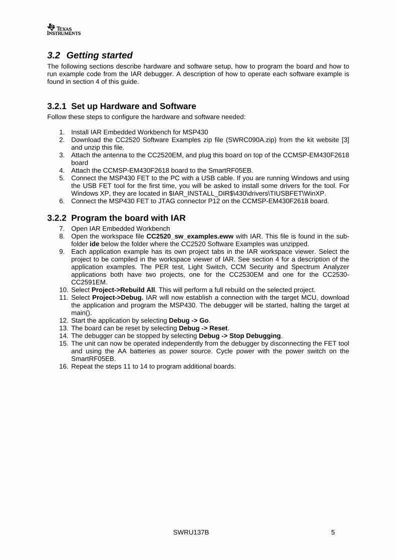
Figure 2 IAR EW
3.2.3 Peripherals used by the example code The application examples utilize various peripherals on the SmartRf05EB i.e. buttons, joystick, LCD, and serial connector. Please refer to CC2520DK User’s Guide for a description of these peripherals. This document is found on the CC2520DK website [3].
3.2.4 Configuring HyperTerminal Some of the application examples outputs to the serial port. The PC HyperTerminal application can be used to display this output. Perform the following steps to configure the HyperTerminal:
1. Start the HyperTerminal application. On Windows XP this is found under the Start menu -> All Programs -> Accessories -> Communications -> HyperTerminal
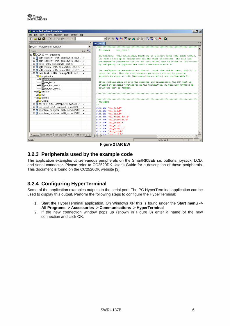
2. If the new connection window pops up (shown in Figure 3) enter a name of the new connection and click OK.
SWRU137B 7
Figure 3 New connection on HyperTerminal
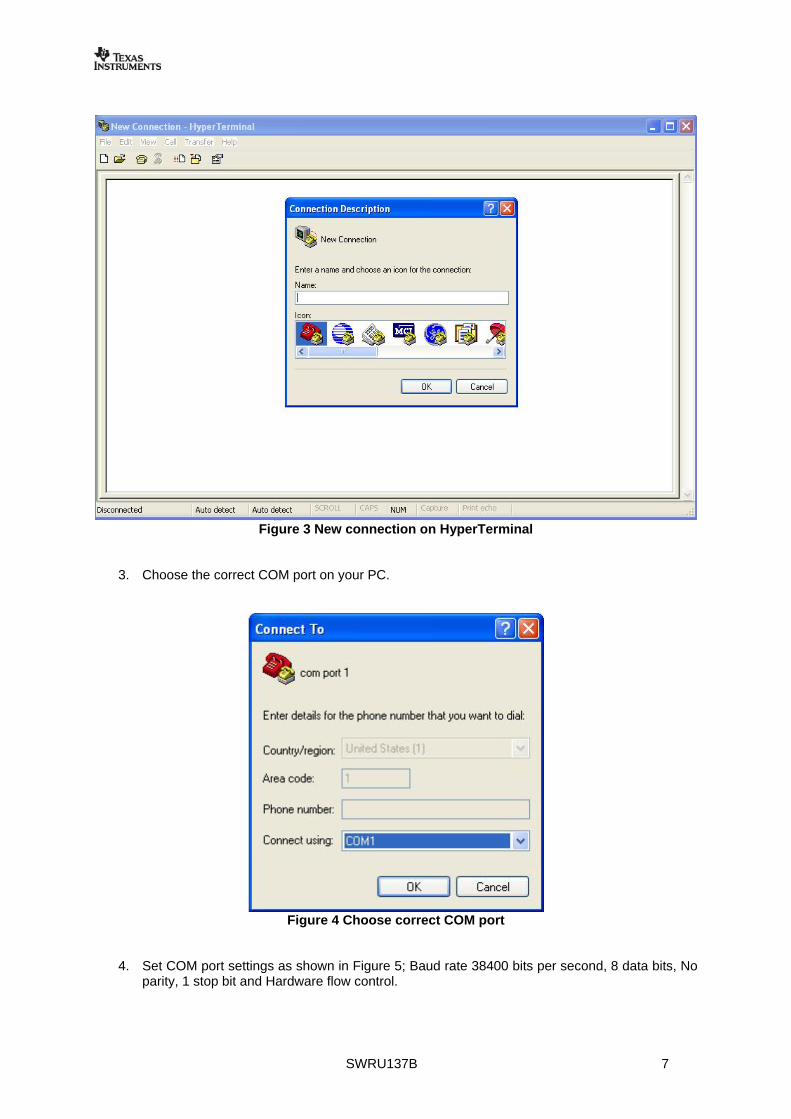
3. Choose the correct COM port on your PC.
Figure 4 Choose correct COM port
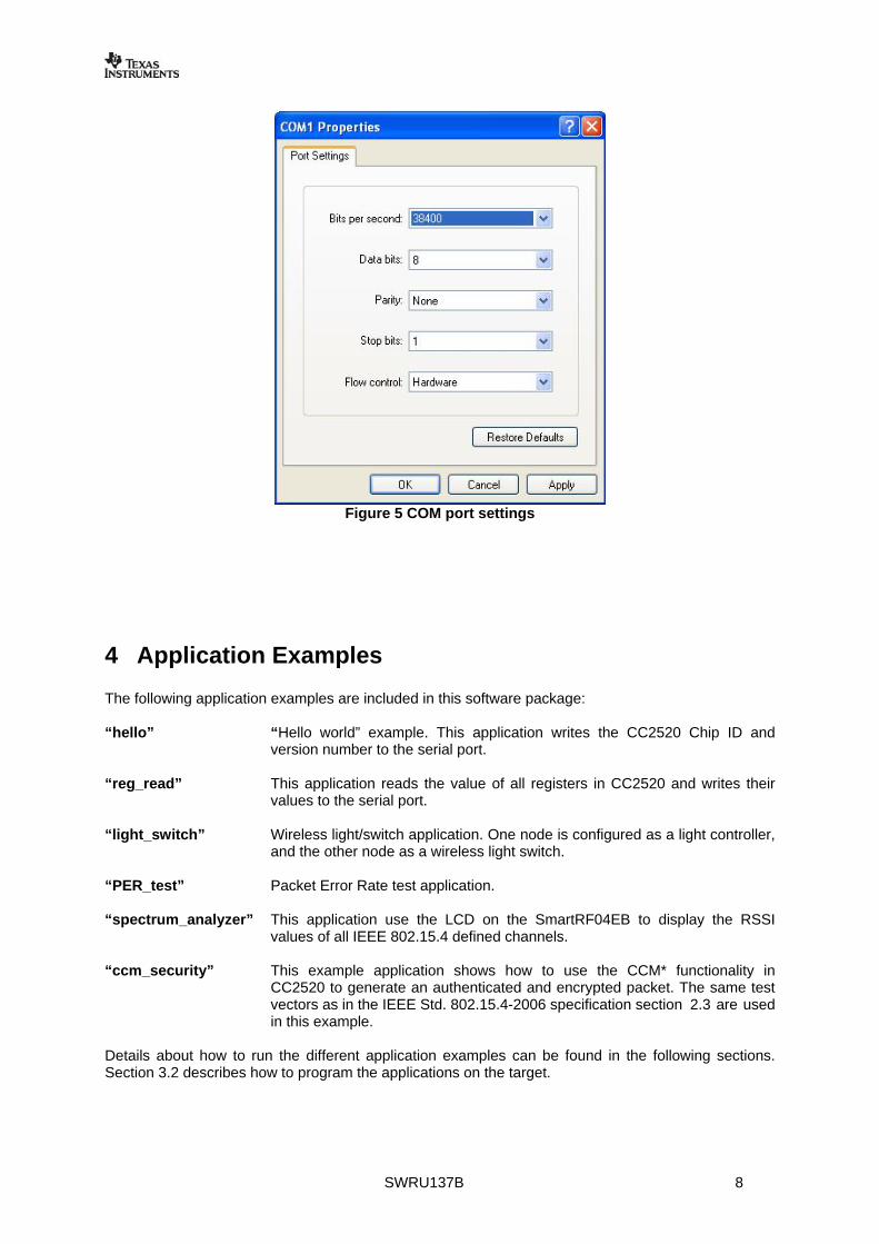
4. Set COM port settings as shown in Figure 5; Baud rate 38400 bits per second, 8 data bits, No parity, 1 stop bit and Hardware flow control.
SWRU137B 8
Figure 5 COM port settings
4 Application Examples The following application examples are included in this software package: “hello” “Hello world” example. This application writes the CC2520 Chip ID and
version number to the serial port. “reg_read” This application reads the value of all registers in CC2520 and writes their
values to the serial port. “light_switch” Wireless light/switch application. One node is configured as a light controller,
and the other node as a wireless light switch. “PER_test” Packet Error Rate test application. “spectrum_analyzer” This application use the LCD on the SmartRF04EB to display the RSSI
values of all IEEE 802.15.4 defined channels. “ccm_security” This example application shows how to use the CCM* functionality in
CC2520 to generate an authenticated and encrypted packet. The same test vectors as in the IEEE Std. 802.15.4-2006 specification section 2.3 are used in this example.
Details about how to run the different application examples can be found in the following sections. Section 3.2 describes how to program the applications on the target.
SWRU137B 9
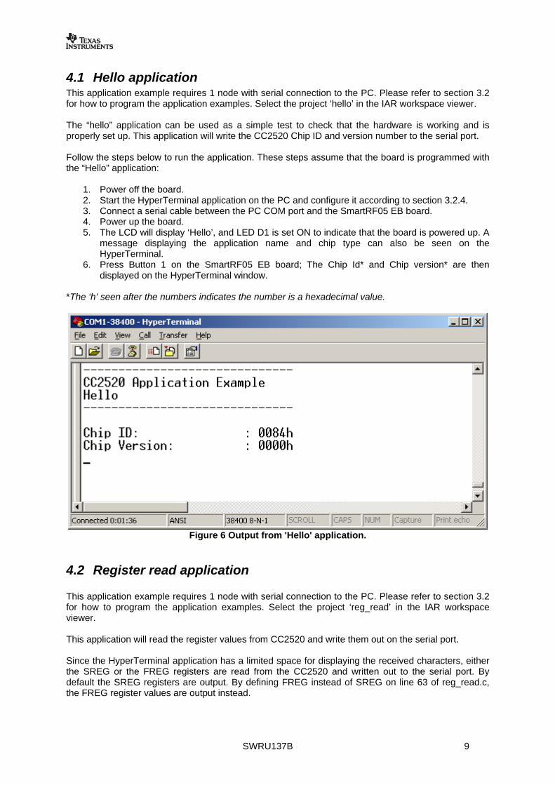
4.1 Hello application This application example requires 1 node with serial connection to the PC. Please refer to section 3.2 for how to program the application examples. Select the project ‘hello’ in the IAR workspace viewer. The “hello” application can be used as a simple test to check that the hardware is working and is properly set up. This application will write the CC2520 Chip ID and version number to the serial port. Follow the steps below to run the application. These steps assume that the board is programmed with the “Hello” application:
1. Power off the board. 2. Start the HyperTerminal application on the PC and configure it according to section 3.2.4. 3. Connect a serial cable between the PC COM port and the SmartRF05 EB board. 4. Power up the board. 5. The LCD will display ‘Hello’, and LED D1 is set ON to indicate that the board is powered up. A
message displaying the application name and chip type can also be seen on the HyperTerminal.
6. Press Button 1 on the SmartRF05 EB board; The Chip Id* and Chip version* are then displayed on the HyperTerminal window.
*The ‘h’ seen after the numbers indicates the number is a hexadecimal value.
Figure 6 Output from 'Hello' application.
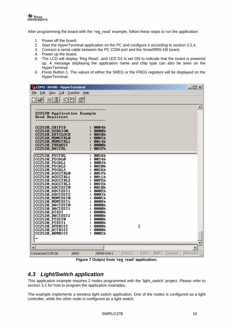
4.2 Register read application This application example requires 1 node with serial connection to the PC. Please refer to section 3.2 for how to program the application examples. Select the project ‘reg_read’ in the IAR workspace viewer. This application will read the register values from CC2520 and write them out on the serial port. Since the HyperTerminal application has a limited space for displaying the received characters, either the SREG or the FREG registers are read from the CC2520 and written out to the serial port. By default the SREG registers are output. By defining FREG instead of SREG on line 63 of reg_read.c, the FREG register values are output instead.
SWRU137B 10
After programming the board with the ‘reg_read’ example, follow these steps to run the application:
1. Power off the board. 2. Start the HyperTerminal application on the PC and configure it according to section 3.2.4. 3. Connect a serial cable between the PC COM port and the SmartRf05 EB board. 4. Power up the board. 5. The LCD will display ‘Reg Read’, and LED D1 is set ON to indicate that the board is powered
up. A message displaying the application name and chip type can also be seen on the HyperTerminal.
6. Press Button 1; The values of either the SREG or the FREG registers will be displayed on the HyperTerminal.
Figure 7 Output from 'reg_read' application.
4.3 Light/Switch application This application example requires 2 nodes programmed with the ‘light_switch’ project. Please refer to section 3.2 for how to program the application examples. The example implements a wireless light switch application. One of the nodes is configured as a light controller, while the other node is configured as a light switch.
SWRU137B 11
The following steps must be done to use the light/switch application:
1. Reset both boards by cycling power. 2. Press Button 1 to enter the application menu 3. Choose device mode. The menu is navigated by moving the joystick right or left. Choose
device mode ‘Switch’ on one of the nodes, and ‘Light’ on the other node. Confirm the choices by pressing Button 1.
4. The light switch application example is now ready. LED D2 on the ‘Light’ node can now be toggled by pressing the joystick on the ‘Switch’.
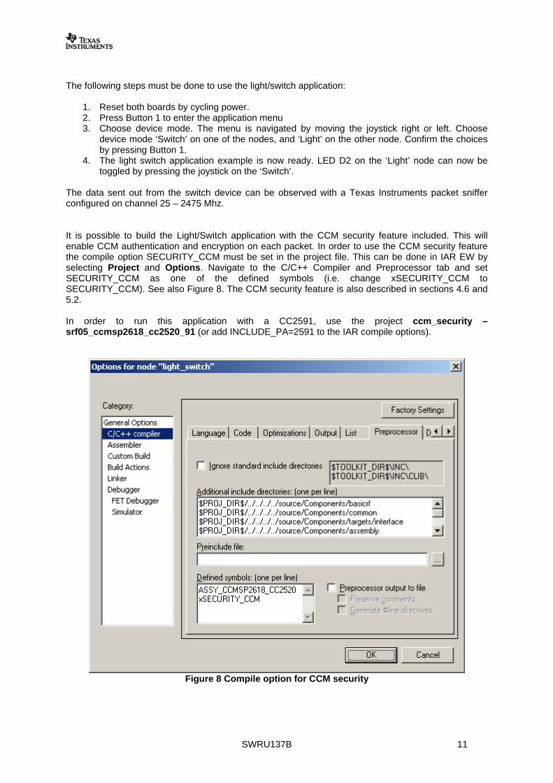
The data sent out from the switch device can be observed with a Texas Instruments packet sniffer configured on channel 25 – 2475 Mhz. It is possible to build the Light/Switch application with the CCM security feature included. This will enable CCM authentication and encryption on each packet. In order to use the CCM security feature the compile option SECURITY_CCM must be set in the project file. This can be done in IAR EW by selecting Project and Options. Navigate to the C/C++ Compiler and Preprocessor tab and set SECURITY_CCM as one of the defined symbols (i.e. change xSECURITY_CCM to SECURITY_CCM). See also Figure 8. The CCM security feature is also described in sections 4.6 and 5.2. In order to run this application with a CC2591, use the project ccm_security – srf05_ccmsp2618_cc2520_91 (or add INCLUDE_PA=2591 to the IAR compile options).
Figure 8 Compile option for CCM security

SWRU137B 12
4.4 Packet Error Rate tester application This application example requires 2 nodes for operation. Select the project ‘per_test’* in the IAR workspace viewer and program both nodes. Please refer to section 3.2 for how to program the boards. *The PER test application is also preprogrammed on both of the CCMSP – EM430F2618 boards found in the CC2520DK. The CC2520DK Quick Start Guide describes how to run the preprogrammed PER test out of the box. The packet error rate test application sets up a one-way RF link between two nodes. One board will operate as a transmitter and the other board will operate as a receiver. The transmitter node will be configured with the number of packets to send as part of the PER test (burst size). During a PER test the receiver node will display the number of received packets, the RSSI (signal strength) level and PER. The user configurable parameters for the test can be seen in Table 1. These parameters are set using a menu on the LCD during initialization. The menu is navigated with the joystick (see arrows in the display) and the settings are confirmed by pressing Button 1.
Parameter Settings Channel 11 – 26 (2405 – 2480 MHz)
Operating Mode Receiver, Transmitter TX Output Power -4 dBm, 0 dBm, 4 dBm *)
Burst Size 1K, 10K, 100K, 1M Table 1 User configurable parameters
*) TX output power with the CC2591: -1dBm, 11dBm, 14dBm, 16dBm and 17dBm
Configure one node as receiver and the other node as transmitter by following the steps below: PER Test Receiver configuration: Perform the following steps to configure the receiver node:
1. Reset the board by cycling power. 2. Press Button 1 to enter the application menu. 3. Select a channel between 11 and 26. Navigate the menu by moving joystick left or right, and
confirm the selection by pressing Button 1. Note the channel, since it will also be used for the Transmitter node.
4. Select operating mode ‘Receiver’ and confirm with Button 1. 5. Select ‘high gain mode’ or ‘low gain mode’ (with CC2591 only) 6. The Receiver node is now ready for operation, displaying ‘Receiver Ready’.
PER Test Transmitter configuration Perform the following steps to configure the transmitter node:
1. Reset the board by cycling power. 2. Press Button 1 to enter the application menu. 3. Select the same channel as for the Receiver node. Navigate the menu by moving the joystick
left or right, and confirm the selection by pressing Button 1. 4. Select operating mode ‘Transmitter’ and confirm with Button 1. 5. Select TX output power by navigating the joystick, either. Confirm with Button 1. 6. Select burst size, either 1000, 10K, 100K or 1M. Press Button 1 to confirm. 7. Push the joystick to start a PER test. The number of packets specified by burst size will be
sent to the Receiver node. Packet Error Rate, RSSI, and number of packets received are displayed on the Receiver’s LCD panel.
8. The PER test is stopped by pushing the joystick.
SWRU137B 13
Calculation of PER and RSSI In order to obtain the statistics during the PER test, the receiver maintains the following variables. The variable rxStats is of type perRxStats_t as defined in per_test.h. rxStats.expectedSeqNum The expected sequence number for the next packet that should
arrive. This is equivalent to the number of received packets+lost packets +1.
rxStats.rssiSum This is the sum of the RSSI level of the last 32 packets. rxStats.rcvdPkts The number of correctly received packets as part of the PER test. rxStats.lostPkts The number of packets that has been lost. Lost packets are detected through a jump in the sequence number. If the received packet has a higher sequence number than rxStats.expectedSeqNum the packets in between are calculated as lost. This implies that a series of lost packets will not be detected until a subsequent packet has been received correctly. The PER value per thousand packets is calculated by the formula:
PER = 1000* rxStats.lostPkts/ (rxStats. lostPkts+ rxStats. rcvdPkts) (for rxStats. rcvdPkts>=1)
The RSSI value is fetched from the first byte following the payload in the received packet. This value is in signed 2’s complement and must be corrected with an RSSI offset to get the absolute RSSI value (in dBm). This offset is specified in the CC2430 datasheet. The converted RSSI values of the last 32 (defined by RSSI_AVG_WINDOW_SIZE in per_test.h) received packets are stored in a ring buffer, implementing a moving average filter. The numbers presented on the LCD are the PER value (line 1) and the average RSSI of the last 32 received packets on line 2.
4.5 Spectrum Analyzer application This application example requires one SmartRF05EB/CCMSP2618/CC2520EM as it merely measures and presents the RSSI values of all IEEE 802.15.4 defined channels in the 2.4 GHz frequency band. The application displays the RSSI values of all channels from 11 (2405 MHz) to 26 (2480 MHz). The application starts up in bar graph mode. In this mode only the bar graphs of the 16 channels are shown. The application displays values in the range -120 dBm to -14 dBm. Text mode adds a textual display of the channel number and the measured value for one specific channel whilst still displaying the bar graphs of all channels, albeit with reduced resolution. The user may toggle between the display modes by moving the joystick up. In text mode the channel is selected by moving the joystick left or right.
4.6 CCM Security application This application example requires 1 node with serial connection to PC for operation. Select the project ‘ccm_security’ in the IAR workspace viewer. Please refer to section 3.2 for how to program the board. The CCM Security example* uses test vectors found in section 2.3 of the IEEE Std. 802.15.4-2006 specification [1]. An authenticated and encrypted packet is generated using CCM*. The resulting packet is transmitted and can be observed on the packet sniffer on channel 25 – 2475 MHz. The plaintext packet can also be modified in the source code and the secured packet can be observed with the packet sniffer. Perform the following steps to run the application:
SWRU137B 14
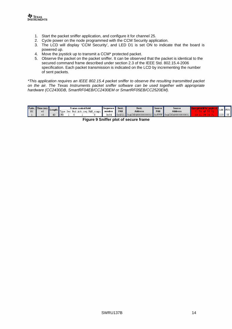
1. Start the packet sniffer application, and configure it for channel 25. 2. Cycle power on the node programmed with the CCM Security application. 3. The LCD will display ‘CCM Security’, and LED D1 is set ON to indicate that the board is
powered up. 4. Move the joystick up to transmit a CCM* protected packet. 5. Observe the packet on the packet sniffer. It can be observed that the packet is identical to the
secured command frame described under section 2.3 of the IEEE Std. 802.15.4-2006 specification. Each packet transmission is indicated on the LCD by incrementing the number of sent packets.
*This application requires an IEEE 802.15.4 packet sniffer to observe the resulting transmitted packet on the air. The Texas Instruments packet sniffer software can be used together with appropriate hardware (CC2430DB, SmartRF04EB/CC2430EM or SmartRF05EB/CC2520EM).
Figure 9 Sniffer plot of secure frame
SWRU137B 15
5 Software Library Reference This section describes the software libraries the application examples are built upon.
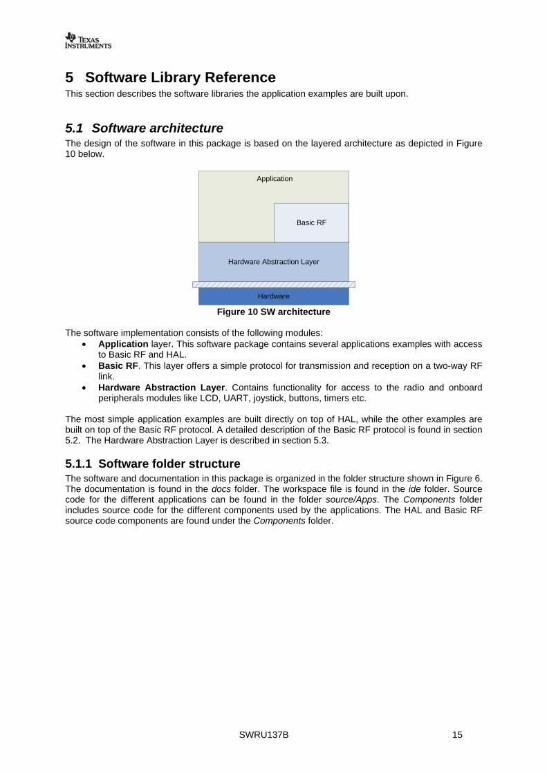
5.1 Software architecture The design of the software in this package is based on the layered architecture as depicted in Figure 10 below.
Application
Basic RF
Hardware Abstraction Layer
Hardware
Figure 10 SW architecture The software implementation consists of the following modules:
• Application layer. This software package contains several applications examples with access to Basic RF and HAL.
• Basic RF. This layer offers a simple protocol for transmission and reception on a two-way RF link.
• Hardware Abstraction Layer. Contains functionality for access to the radio and onboard peripherals modules like LCD, UART, joystick, buttons, timers etc.
The most simple application examples are built directly on top of HAL, while the other examples are built on top of the Basic RF protocol. A detailed description of the Basic RF protocol is found in section 5.2. The Hardware Abstraction Layer is described in section 5.3.
5.1.1 Software folder structure The software and documentation in this package is organized in the folder structure shown in Figure 6. The documentation is found in the docs folder. The workspace file is found in the ide folder. Source code for the different applications can be found in the folder source/Apps. The Components folder includes source code for the different components used by the applications. The HAL and Basic RF source code components are found under the Components folder.
SWRU137B 16
docs
CC2520_APP_EX
ide
source
Apps
Components
ccm_security
hello
light_switch
PER_test
reg_read
spectrum_analyzer
Figure 11 Software folder structure
5.2 Basic RF The Basic RF layer offers a simple protocol for transmission and reception on a two-way RF link. The Basic RF protocol offers service for packet transmission and reception. It also offers secure communication by use of CCM-64 authentication and encryption/decryption of packets. The security features of Basic RF can be compiled in by defining the compile switch SECURITY_CCM in the project file. The compile time inclusion of security features is done to save code space for the applications where security features are not needed. The protocol uses IEEE 802.15.4 MAC compliant data and acknowledgment packets. However it does not offer a full MAC layer, only a simple data link layer for communication between two nodes. See also section 5.2.5 for limitations of Basic RF. Basic RF contains only a small subset of the 802.15.4 standard:
• Association, scanning or beacons are not implemented • No defined coordinator/device roles (peer-to-peer, all nodes are equal) • Waits for the channel to become ready, but does not check CCA twice (IEEE 802.15.4 CSMA-
CA) • No packet retransmission. This must be taken care of by the layer above Basic RF.
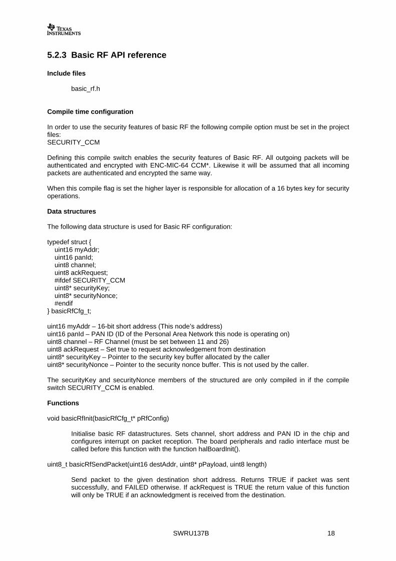
5.2.1 Basic RF frame format
Octets: 1 2 1 2 2 2 5 Variable 2
Length Byte
Frame Control
Sequence number
Dest. PAN ID
Dest. Address
Source Address
Aux.Sec. Header
Frame payload FCS

SWRU137B 17
Figure 12 Basic RF frame format The frame format of the Basic RF protocol is shown in Figure 12. The first byte is a length byte. The length byte itself is not counted in the length. The frame control field is set according to the IEEE Std. 802.15.4-2006. Please refer to section 7.2 in the IEEE Std. 802.15.4-2006 [1]. The sequence number is an 8 bit value starting on 0 for the first packet transmitted after initialization. The values of the destination PAN ID, destination address and source address fields are configured by the application as part of the basic RF initialization. Please refer to the Basic RF API section 5.2.3 for further information. The auxiliary security header is only included in the frames when the security features of Basic RF is used i.e when the compile option SECURITY_CCM is set in the project file. This field is 5 bytes long and consists of a security control byte that defines the level of protection applied to this frame, and frame counter. The Basic RF protocol supports only one security mode: ENC-MIC-64 i.e. encryption and authentication with 64 bits Message Integrity Code. For this mode the Security Control field is set to 0x06 according to IEEE Std. 802.15.4-2006 [1]. The frame counter field of the auxiliary security header is 4 bytes long and is used for replay protection of the frame. The value of the frame counter field is set to 0 on initialization and incremented for each transmitted packet. The frame payload is variable in length and consists of data sent from the layer above Basic RF. The maximum length of this field is 103 Bytes. The Frame Check Sequence field (FCS) is 2 bytes long. This field is automatically appended by the radio chip, and is not taken care of by the Basic RF layer. When a frame is received the first byte is replaced with the RSSI value in the RX FIFO on the radio.
5.2.2 Basic RF usage instructions Startup
1. Make sure that the board peripherals and radio interface is initialized i.e. halBoardInit() must have been called first.
2. Create a basicRfCfg_t structure, and initialize its members. If the security features of Basic RF are used, the higher layer is responsible for allocating and assigning the 16 bytes key.
3. Call basicRfInit() to initialize the packet protocol. Transmission:
1. Create a buffer with the payload to send. Maximum payload size for Basic RF is 103 Bytes. 2. Call basicRfSendPacket(). Check the return value.
Reception:
1. Perform polling by calling basicRfPacketIsReady() to check if a new packet is ready to be received by the higher layer.
2. Call basicRfReceive() to receive the packet by higher layer. The caller is responsible for allocating a buffer large enough for the packet and 2 Bytes buffer space for the RSSI value.
By calling basicRfReceiveOn() the radio receiver is kept on all the time. This is done for nodes that need to be able to receive packets at any time. The drawback is a higher current consumption. By calling basicRfReceiveOff() the radio receiver is turned off. It is only turned on again during CCA for packet transmission.
SWRU137B 18
5.2.3 Basic RF API reference Include files
basic_rf.h
Compile time configuration In order to use the security features of basic RF the following compile option must be set in the project files: SECURITY_CCM Defining this compile switch enables the security features of Basic RF. All outgoing packets will be authenticated and encrypted with ENC-MIC-64 CCM*. Likewise it will be assumed that all incoming packets are authenticated and encrypted the same way. When this compile flag is set the higher layer is responsible for allocation of a 16 bytes key for security operations. Data structures The following data structure is used for Basic RF configuration: typedef struct { uint16 myAddr; uint16 panId; uint8 channel; uint8 ackRequest; #ifdef SECURITY_CCM uint8* securityKey; uint8* securityNonce; #endif } basicRfCfg_t; uint16 myAddr – 16-bit short address (This node’s address) uint16 panId – PAN ID (ID of the Personal Area Network this node is operating on) uint8 channel – RF Channel (must be set between 11 and 26) uint8 ackRequest – Set true to request acknowledgement from destination uint8* securityKey – Pointer to the security key buffer allocated by the caller uint8* securityNonce – Pointer to the security nonce buffer. This is not used by the caller. The securityKey and securityNonce members of the structured are only compiled in if the compile switch SECURITY_CCM is enabled. Functions void basicRfInit(basicRfCfg_t* pRfConfig)
Initialise basic RF datastructures. Sets channel, short address and PAN ID in the chip and configures interrupt on packet reception. The board peripherals and radio interface must be called before this function with the function halBoardInit().
uint8_t basicRfSendPacket(uint16 destAddr, uint8* pPayload, uint8 length)
Send packet to the given destination short address. Returns TRUE if packet was sent successfully, and FAILED otherwise. If ackRequest is TRUE the return value of this function will only be TRUE if an acknowledgment is received from the destination.
SWRU137B 19
uint8 basicRfPacketIsReady(void) Returns TRUE if a received packet is ready to be retrieved by higher layer. uint8 basicRfReceive(uint8* pRxData, uint8 len, int16* pRssi)
Retrieve packet from basic RF layer. The caller is responsible for allocating buffer space for data and the RSSI value.
void basicRfReceiveOn(void)
Turn on receiver on radio. After calling this function the radio is kept on until basicRfReceiveOff is called.
void basicRfReceiveOff(void) Turn off receiver on radio, and keep it off unless for transmitting a packet with Clear Channel Assessment.
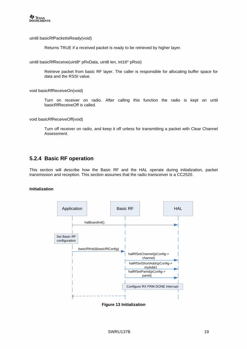
5.2.4 Basic RF operation This section will describe how the Basic RF and the HAL operate during initialization, packet transmission and reception. This section assumes that the radio transceiver is a CC2520. Initialization
Application Basic RF HAL
halBoardInit()
Set Basic RF configuration
basicRfInit(&basicRfConfig)halRfSetChannel(pConfig->
channel)halRfSetShortAddr(pConfig->
myAddr)halRfSetPanId(pConfig->
panId)
Configure RX FRM DONE Interrupt
Figure 13 Initialization
SWRU137B 20
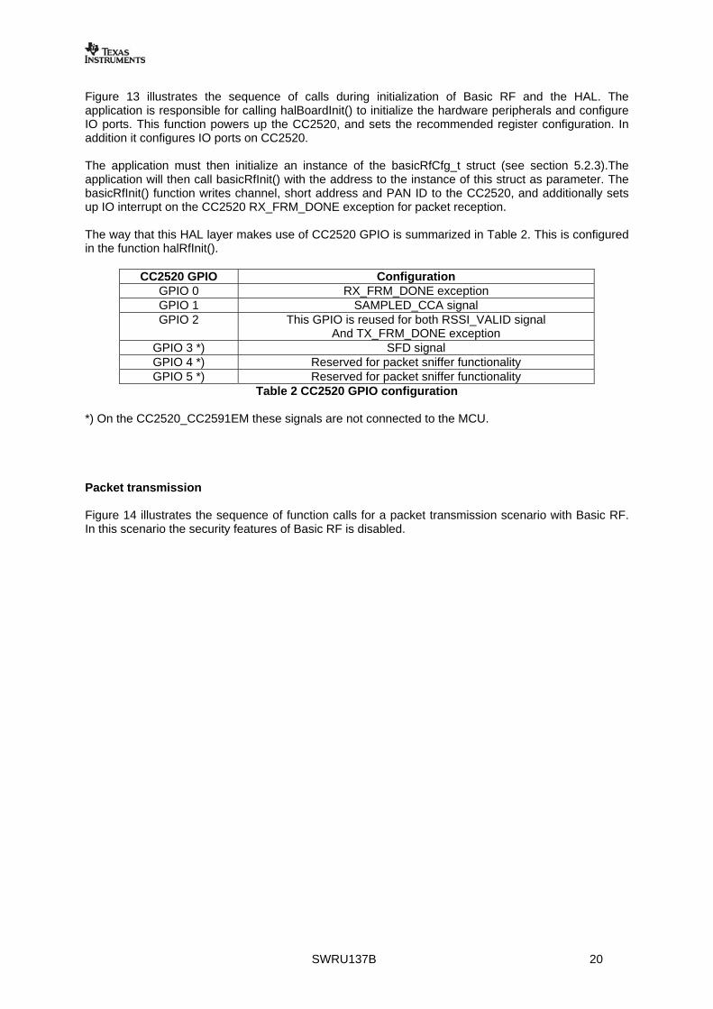
Figure 13 illustrates the sequence of calls during initialization of Basic RF and the HAL. The application is responsible for calling halBoardInit() to initialize the hardware peripherals and configure IO ports. This function powers up the CC2520, and sets the recommended register configuration. In addition it configures IO ports on CC2520. The application must then initialize an instance of the basicRfCfg_t struct (see section 5.2.3).The application will then call basicRfInit() with the address to the instance of this struct as parameter. The basicRfInit() function writes channel, short address and PAN ID to the CC2520, and additionally sets up IO interrupt on the CC2520 RX_FRM_DONE exception for packet reception. The way that this HAL layer makes use of CC2520 GPIO is summarized in Table 2. This is configured in the function halRfInit().
CC2520 GPIO Configuration
GPIO 0 RX_FRM_DONE exception GPIO 1 SAMPLED_CCA signal GPIO 2 This GPIO is reused for both RSSI_VALID signal
And TX_FRM_DONE exception GPIO 3 *) SFD signal GPIO 4 *) Reserved for packet sniffer functionality GPIO 5 *) Reserved for packet sniffer functionality
Table 2 CC2520 GPIO configuration
*) On the CC2520_CC2591EM these signals are not connected to the MCU. Packet transmission Figure 14 illustrates the sequence of function calls for a packet transmission scenario with Basic RF. In this scenario the security features of Basic RF is disabled.
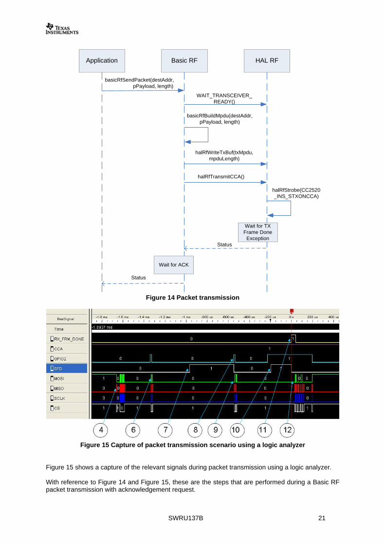
SWRU137B 21
Application Basic RF HAL RF
basicRfSendPacket(destAddr, pPayload, length)
halRfWriteTxBuf(txMpdu, mpduLength)
halRfTransmitCCA()
Wait for ACK
basicRfBuildMpdu(destAddr, pPayload, length)
Status
Status
WAIT_TRANSCEIVER_READY()
halRfStrobe(CC2520_INS_STXONCCA)
Wait for TX Frame Done
Exception
Figure 14 Packet transmission
Figure 15 Capture of packet transmission scenario using a logic analyzer
Figure 15 shows a capture of the relevant signals during packet transmission using a logic analyzer. With reference to Figure 14 and Figure 15, these are the steps that are performed during a Basic RF packet transmission with acknowledgement request.
SWRU137B 22
1. The application prepares the payload to be sent and calls the function basicRfSend() with the
16 bit destination address, a reference to the payload buffer and the length of the payload buffer as arguments.
2. Basic RF checks that the transceiver is idle with the macro WAIT_TRANSCEIVER_READY(). This macro measures the SFD (Start of Frame Delimiter) which in the initialization routine (halRfInit()) is configured to be output on GPIO3 on CC2520 (using GPIO2 with CC2591).
3. Basic RF calls the function basicRfBuildMpdu(). Basic Rf keeps an internal buffer for the outgoing MPDU. It will first build the header with the correct address and header information, and then it will copy the payload from the application over to the remaining part of the internal buffer.
4. Basic RF will then call halRfWriteTxBuf() to write the MPDU to the CC2520 TX buffer. The activity on the SPI bus can be seen on marker 4 in Figure 15.
5. The function halRfTransmitCCA() is called to transmit a packet with CCA on the air. 6. GPIO2 is reused for both CC2520 TX_FRM_DONE exception and for RSSI_VALID signal.
The SPI activity on marker 6 in Figure 15 is due to reconfiguration CC2520 to output TX_FRM_DONE exception and for sending the strobe command CC2520_INS_STXONCCA. If the CCA signal is high, the packet can successfully be transmitted on the air.
7. The SFD signal goes high meaning that the packet transmission has started. 8. The function halRFTransmitCCA() will wait until the TX_FRM_DONE exception is set
(Low to high transition on GPIO2). 9. The SPI activity on marker 9 is due to reconfiguration of GPIO2 back to RSSI_VALID
again. 10. The SFD signal goes high again because of the incoming ACK from the destination. 11. RX_FRM_DONE exception is set because of the incoming ACK. 12. The basicRfFrmDoneISR() interrupt service routine starts reading out the ACK packet
from the CC2520 RX buffer. This can as the activity on the SPI bus on marker 12 in Figure 15.
13. If the ACK is successfully received within a predefined waiting time, the basicRfSend() returns with status SUCCESS to the application.
SWRU137B 23
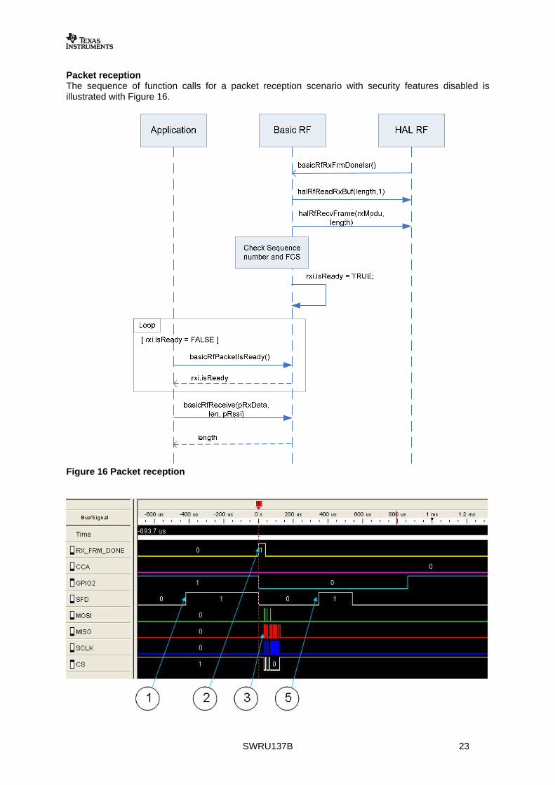
Packet reception The sequence of function calls for a packet reception scenario with security features disabled is illustrated with Figure 16.
Figure 16 Packet reception
SWRU137B 24
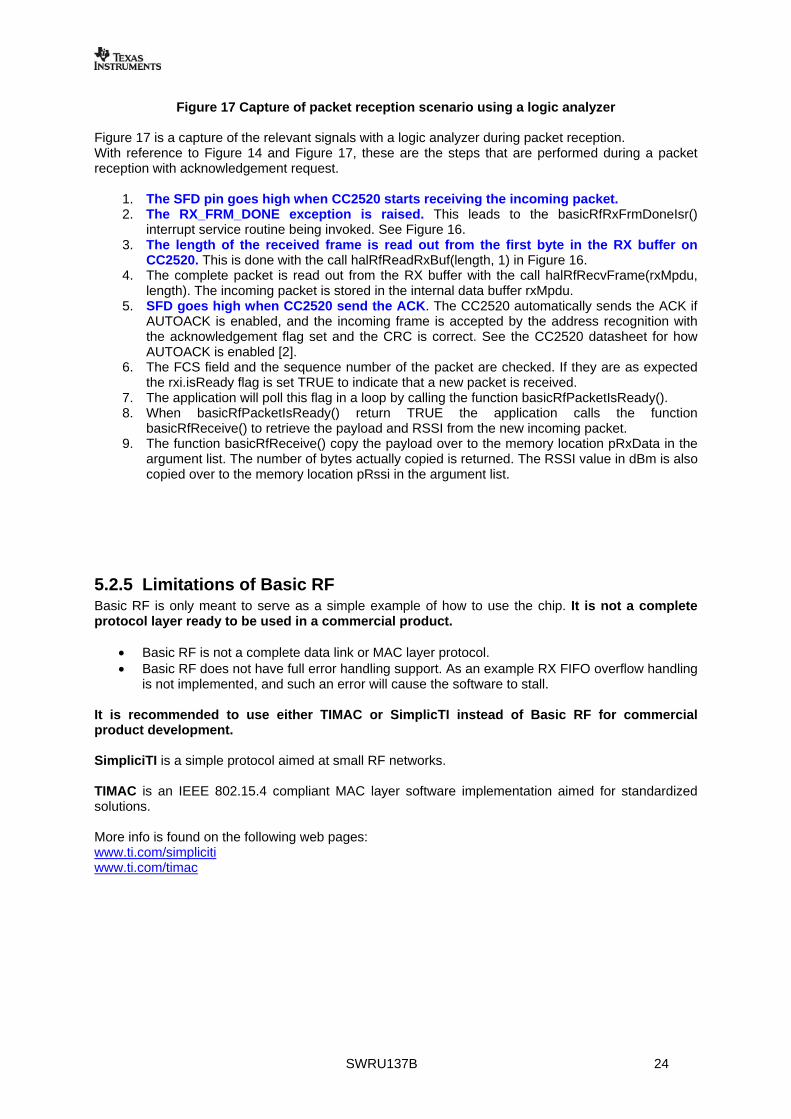
Figure 17 Capture of packet reception scenario using a logic analyzer Figure 17 is a capture of the relevant signals with a logic analyzer during packet reception. With reference to Figure 14 and Figure 17, these are the steps that are performed during a packet reception with acknowledgement request.
1. The SFD pin goes high when CC2520 starts receiving the incoming packet. 2. The RX_FRM_DONE exception is raised. This leads to the basicRfRxFrmDoneIsr()
interrupt service routine being invoked. See Figure 16. 3. The length of the received frame is read out from the first byte in the RX buffer on
CC2520. This is done with the call halRfReadRxBuf(length, 1) in Figure 16. 4. The complete packet is read out from the RX buffer with the call halRfRecvFrame(rxMpdu,
length). The incoming packet is stored in the internal data buffer rxMpdu. 5. SFD goes high when CC2520 send the ACK. The CC2520 automatically sends the ACK if
AUTOACK is enabled, and the incoming frame is accepted by the address recognition with the acknowledgement flag set and the CRC is correct. See the CC2520 datasheet for how AUTOACK is enabled [2].
6. The FCS field and the sequence number of the packet are checked. If they are as expected the rxi.isReady flag is set TRUE to indicate that a new packet is received.
7. The application will poll this flag in a loop by calling the function basicRfPacketIsReady(). 8. When basicRfPacketIsReady() return TRUE the application calls the function
basicRfReceive() to retrieve the payload and RSSI from the new incoming packet. 9. The function basicRfReceive() copy the payload over to the memory location pRxData in the
argument list. The number of bytes actually copied is returned. The RSSI value in dBm is also copied over to the memory location pRssi in the argument list.
5.2.5 Limitations of Basic RF Basic RF is only meant to serve as a simple example of how to use the chip. It is not a complete protocol layer ready to be used in a commercial product.
• Basic RF is not a complete data link or MAC layer protocol. • Basic RF does not have full error handling support. As an example RX FIFO overflow handling
is not implemented, and such an error will cause the software to stall. It is recommended to use either TIMAC or SimplicTI instead of Basic RF for commercial product development. SimpliciTI is a simple protocol aimed at small RF networks. TIMAC is an IEEE 802.15.4 compliant MAC layer software implementation aimed for standardized solutions. More info is found on the following web pages: www.ti.com/simpliciti www.ti.com/timac
SWRU137B 25
5.3 Hardware Abstraction Layer
5.3.1 HAL RF API reference Include files
hal_rf.h hal_rf_security.h
Functions uint8 halRfInit(void)
Powers up the radio, configures the radio with recommended register settings, enables autoack and configures the IO on the radio. This function must be called after halBoardInit().
uint8 halRfSetPower(uint8 power) Set TX output power. uint8 halRfTransmit(void) Transmit a frame. The TX FIFO must have been written before this function is called. uint8 halRfGetChipId(void) Return radio chip ID. uint8 halRfGetChipVer(void) Return radio chip version. uint8 halRfGetRandomByte(void) Return random byte. uint8 halRfGetRssiOffset(void) Return RSSI offset for radio. void halRfWriteTxBuf(uint8* data, uint8 length)
Write the number of bytes given by length from the memory location pointed to by the pointer data to the radio TX buffer.
void halRfReadRxBuf(uint8* data, uint8 length)
SWRU137B 26
Read the number of bytes given by length from radio RX buffer to the memory location pointed to by the pointer data. The radio status byte is returned.
void halRfWaitTransceiverReady(void) Wait until the transceiver is ready. void halRfReceiveOn(void) Turn on receiver on radio. void halRfReceiveOff(void) Turn off receiver on radio. void halRfDisableRxInterrupt(void) Clear and disable RX interrupt. void halRfEnableRxInterrupt(void) Enable RX interrupt. void halRfRxInterruptConfig(ISR_FUNC_PTR pf) Configure RX interrupt, and setting the function to be called on interrupt. void halRfSetChannel(uint8 channel) Set RF channel. Channel must be in the range 11-26. void halRfSetShortAddr(uint16 shortAddr) Write 16 bit short address to the radio. void halRfSetPanId(uint16 PanId) Write 16 bit PAN ID to the radio. Security Interface void halRfSecurityInit(uint8* key, uint8* nonceRx, uint8* nonceTx)
Write 16 bit nonces and key to to the radio from the memory locations pointed to by key, nonceRx and nonceTx.
uint8 halRfReadRxBufSecure(uint8* pData, uint8 length, uint8 encrLength, uint8 authLength, uint8 m)
SWRU137B 27
Read out RX buffer from radio with CCM authentication and decryption. void halRfWriteTxBufSecure(uint8* pData, uint8 length, uint8 encrLength, uint8 authLength, uint8 m) Write to TX buffer in radio with CCM authentication and encryption. void halRfIncNonceTx(void)
Increment the frame counter field of the nonce used for outgoing packets. Refer to IEEE Std. 802.15.4-2006 [1] for a description of this field.
References
[1] IEEE Std. 802.15.4-2006, Wireless Medium Access Control (MAC) and Physical Layer (PHY) Specifications for Low-Rate Wireless Personal Area Networks (WPANs)
[2] CC2520 datasheet (SWRS068)
[3] CC2520DK website: www.ti.com/cc2520dk
Document History
Revision Date Description/Changes - 2007-12-14 Initial release A 2008-09-18 Revison A B 2009-10-28 Changed output power values for new CC2520-CC2591EM
IMPORTANT NOTICETexas Instruments Incorporated and its subsidiaries (TI) reserve the right to make corrections, modifications, enhancements, improvements,and other changes to its products and services at any time and to discontinue any product or service without notice. Customers shouldobtain the latest relevant information before placing orders and should verify that such information is current and complete. All products aresold subject to TI’s terms and conditions of sale supplied at the time of order acknowledgment.TI warrants performance of its hardware products to the specifications applicable at the time of sale in accordance with TI’s standardwarranty. Testing and other quality control techniques are used to the extent TI deems necessary to support this warranty. Except wheremandated by government requirements, testing of all parameters of each product is not necessarily performed.TI assumes no liability for applications assistance or customer product design. Customers are responsible for their products andapplications using TI components. To minimize the risks associated with customer products and applications, customers should provideadequate design and operating safeguards.TI does not warrant or represent that any license, either express or implied, is granted under any TI patent right, copyright, mask work right,or other TI intellectual property right relating to any combination, machine, or process in which TI products or services are used. Informationpublished by TI regarding third-party products or services does not constitute a license from TI to use such products or services or awarranty or endorsement thereof. Use of such information may require a license from a third party under the patents or other intellectualproperty of the third party, or a license from TI under the patents or other intellectual property of TI.Reproduction of TI information in TI data books or data sheets is permissible only if reproduction is without alteration and is accompaniedby all associated warranties, conditions, limitations, and notices. Reproduction of this information with alteration is an unfair and deceptivebusiness practice. TI is not responsible or liable for such altered documentation. Information of third parties may be subject to additionalrestrictions.Resale of TI products or services with statements different from or beyond the parameters stated by TI for that product or service voids allexpress and any implied warranties for the associated TI product or service and is an unfair and deceptive business practice. TI is notresponsible or liable for any such statements.TI products are not authorized for use in safety-critical applications (such as life support) where a failure of the TI product would reasonablybe expected to cause severe personal injury or death, unless officers of the parties have executed an agreement specifically governingsuch use. Buyers represent that they have all necessary expertise in the safety and regulatory ramifications of their applications, andacknowledge and agree that they are solely responsible for all legal, regulatory and safety-related requirements concerning their productsand any use of TI products in such safety-critical applications, notwithstanding any applications-related information or support that may beprovided by TI. Further, Buyers must fully indemnify TI and its representatives against any damages arising out of the use of TI products insuch safety-critical applications.TI products are neither designed nor intended for use in military/aerospace applications or environments unless the TI products arespecifically designated by TI as military-grade or "enhanced plastic." Only products designated by TI as military-grade meet militaryspecifications. Buyers acknowledge and agree that any such use of TI products which TI has not designated as military-grade is solely atthe Buyer's risk, and that they are solely responsible for compliance with all legal and regulatory requirements in connection with such use.TI products are neither designed nor intended for use in automotive applications or environments unless the specific TI products aredesignated by TI as compliant with ISO/TS 16949 requirements. Buyers acknowledge and agree that, if they use any non-designatedproducts in automotive applications, TI will not be responsible for any failure to meet such requirements.Following are URLs where you can obtain information on other Texas Instruments products and application solutions:Products ApplicationsAmplifiers amplifier.ti.com Audio www.ti.com/audioData Converters dataconverter.ti.com Automotive www.ti.com/automotiveDLP® Products www.dlp.com Broadband www.ti.com/broadbandDSP dsp.ti.com Digital Control www.ti.com/digitalcontrolClocks and Timers www.ti.com/clocks Medical www.ti.com/medicalInterface interface.ti.com Military www.ti.com/militaryLogic logic.ti.com Optical Networking www.ti.com/opticalnetworkPower Mgmt power.ti.com Security www.ti.com/securityMicrocontrollers microcontroller.ti.com Telephony www.ti.com/telephonyRFID www.ti-rfid.com Video & Imaging www.ti.com/videoRF/IF and ZigBee® Solutions www.ti.com/lprf Wireless www.ti.com/wireless
Mailing Address: Texas Instruments, Post Office Box 655303, Dallas, Texas 75265Copyright © 2009, Texas Instruments Incorporated