Embed Size (px)
Citation preview
Ken-ya HashimotoChiba University
[email protected]://www.te.chiba-u.jp/~ken
Part 7: Basics of RF Circuits
Introduction to Surface Acoustic Wave (SAW) Devices
April 2, 2019
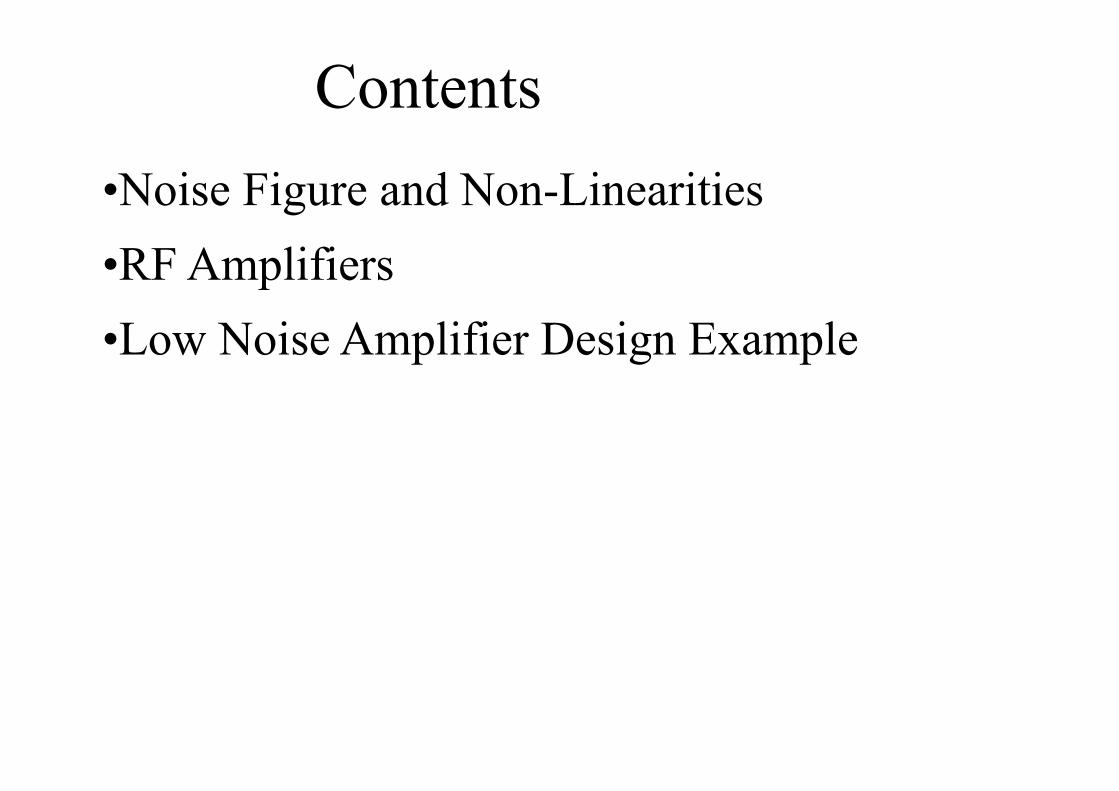
•Noise Figure and Non-Linearities•RF Amplifiers•Low Noise Amplifier Design Example
Contents
•Noise Figure and Non-Linearities•RF Amplifiers•Low Noise Amplifier Design Example
Contents
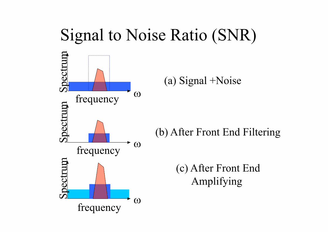
Signal to Noise Ratio (SNR)
frequency
Spec
trum
frequency
Spec
trum
frequency
Spec
trum
(a) Signal +Noise
(b) After Front End Filtering
(c) After Front End Amplifying
ioo
ii
NN
NSNSF 1
//
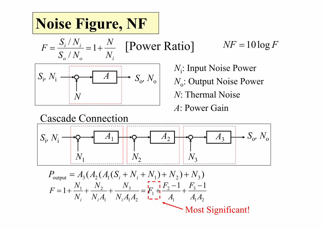
Noise Figure, NFFNF log10[Power Ratio]
Most Significant!
Cascade Connection
)))((( 321123output NNNNSAAAP ii
21
3
1
21
21
3
1
21 111AA
FA
FFAAN
NAN
NNNF
iii
Si, NiSo, NoA3A2A1
N3N2N1
Si, Ni So, NoA
N
Ni: Input Noise PowerNo: Output Noise PowerN: Thermal NoiseA: Power Gain
Input Power Level (dBm)Out
put P
ower
Lev
el(d
Bm
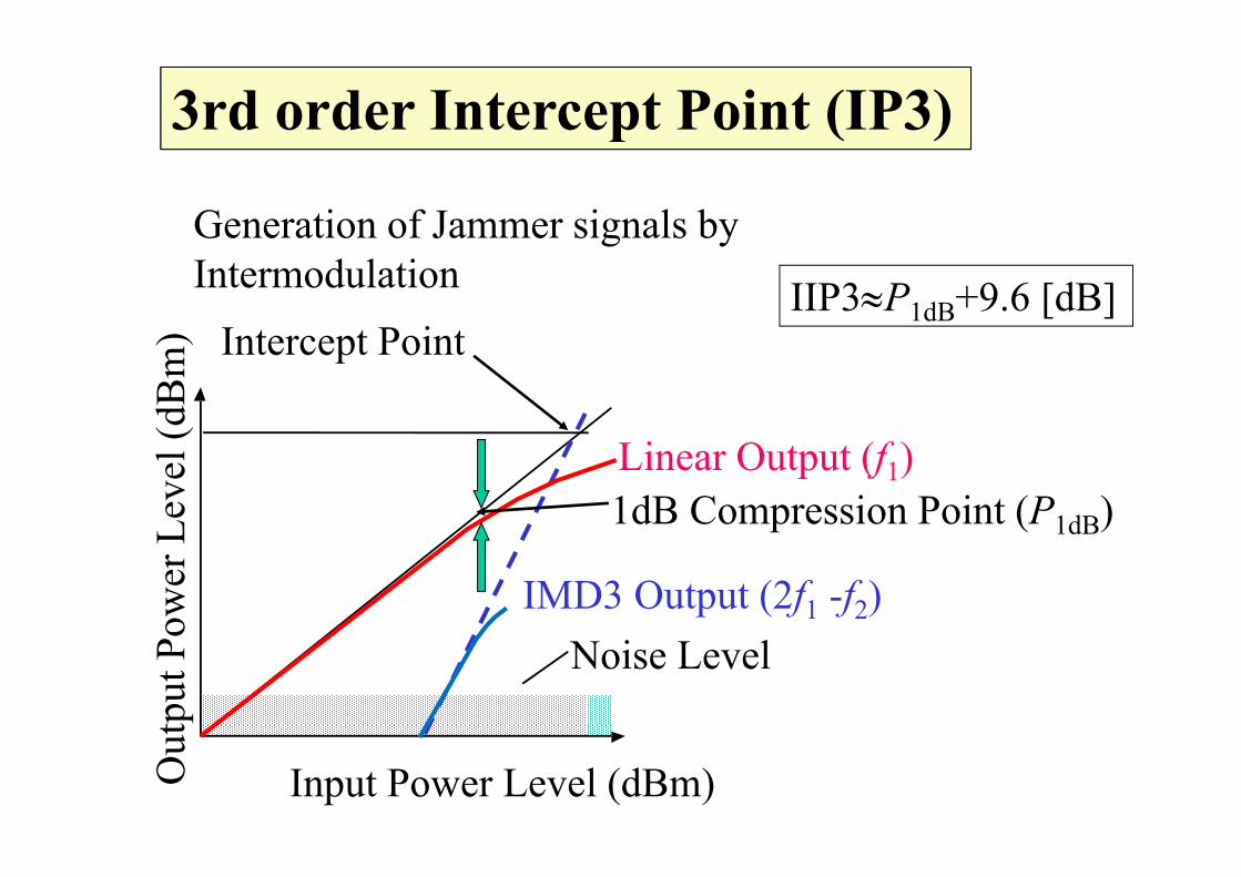
) Intercept Point
Linear Output (f1)
IMD3 Output (2f1 -f2)Noise Level
3rd order Intercept Point (IP3)
Generation of Jammer signals by Intermodulation
1dB Compression Point (P1dB)
IIP3P1dB+9.6 [dB]
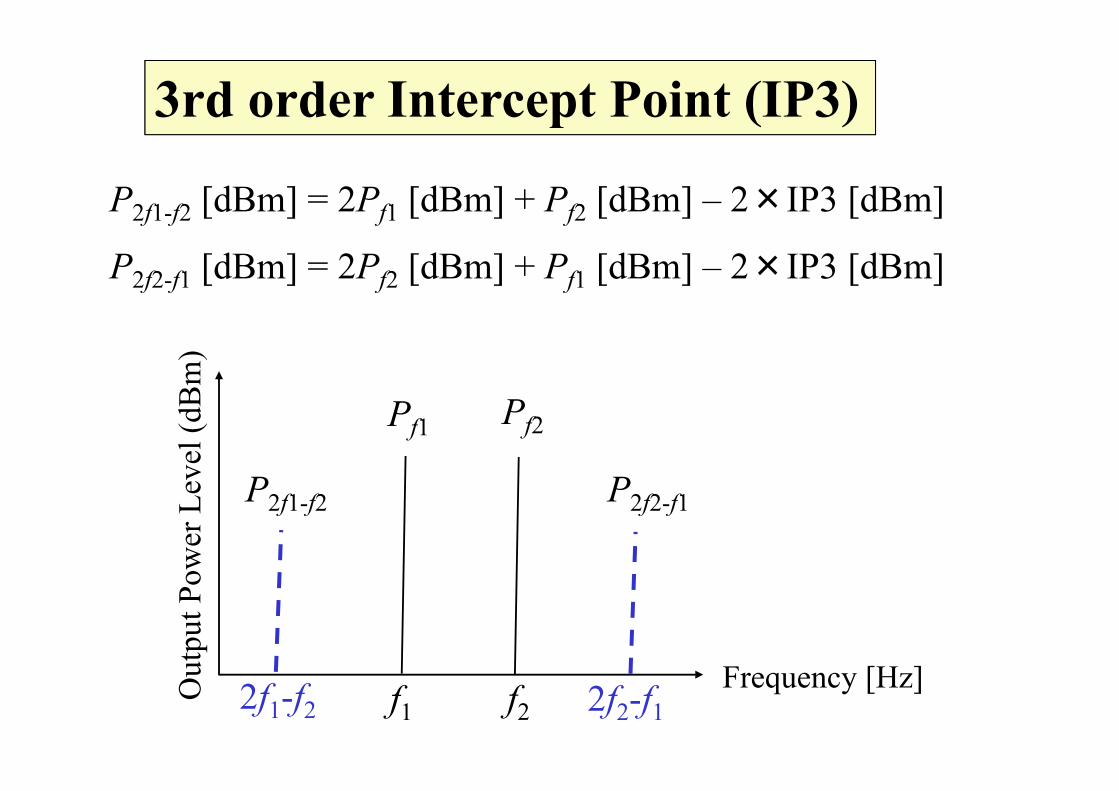
2f1-f2
3rd order Intercept Point (IP3)
P2f1-f2 [dBm] = 2Pf1 [dBm] + Pf2 [dBm] – 2×IP3 [dBm]
P2f2-f1 [dBm] = 2Pf2 [dBm] + Pf1 [dBm] – 2×IP3 [dBm]
P2f2-f1P2f1-f2
Pf1 Pf2
Frequency [Hz]Out
put P
ower
Lev
el(d
Bm
)
2f2-f1f1 f2
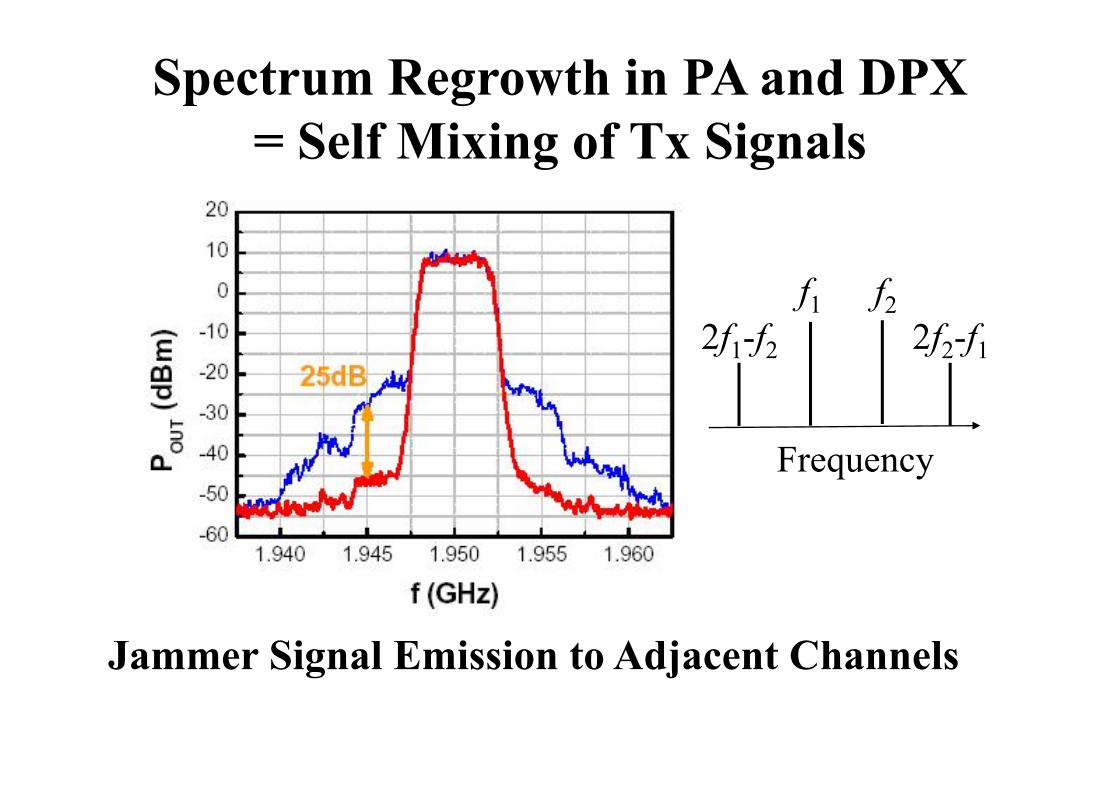
Spectrum Regrowth in PA and DPX= Self Mixing of Tx Signals
Jammer Signal Emission to Adjacent Channels
Frequency
f1 f22f2-f12f1-f2
f2-f1
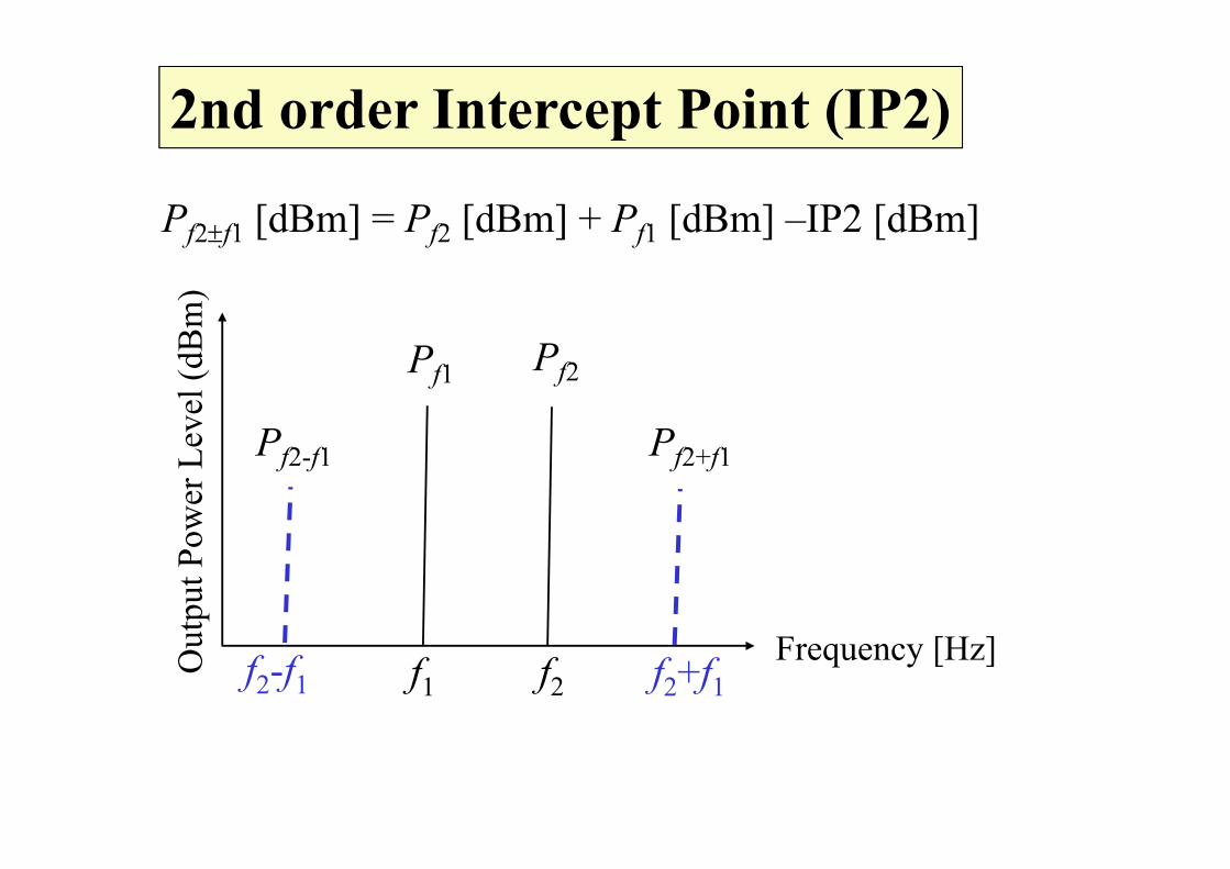
2nd order Intercept Point (IP2)
Pf2f1 [dBm] = Pf2 [dBm] + Pf1 [dBm] –IP2 [dBm]
Pf2+f1Pf2-f1
Pf1 Pf2
Frequency [Hz]Out
put P
ower
Lev
el(d
Bm
)
f2+f1f1 f2
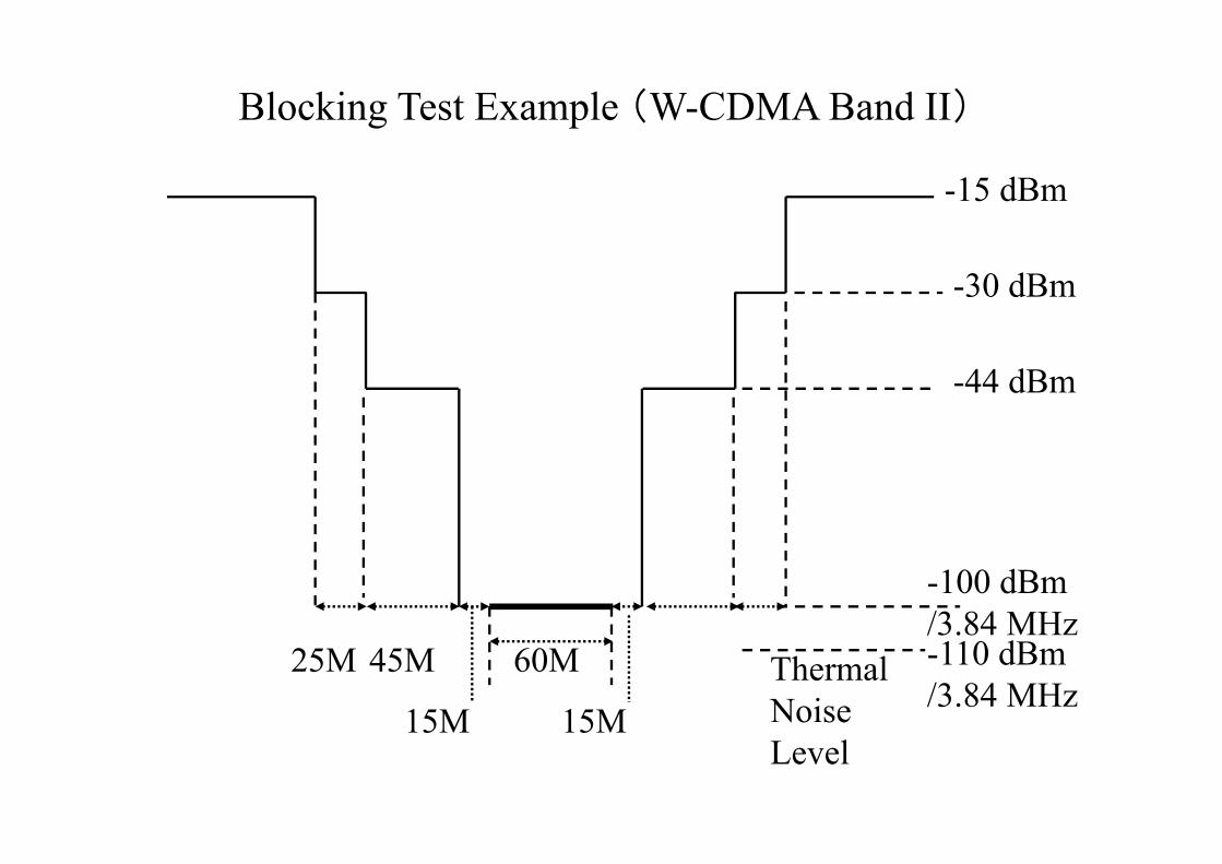
-30 dBm
-15 dBm
-44 dBm
15M
45M
-100 dBm/3.84 MHz
60M
15M
25M
Blocking Test Example (W-CDMA Band II)
-110 dBm/3.84 MHz
Thermal Noise Level
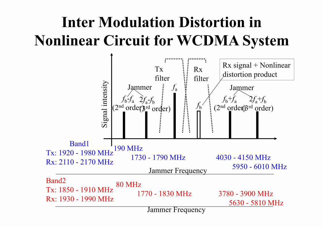
Inter Modulation Distortion in Nonlinear Circuit for WCDMA System
Sign
al in
tens
ity fa
fb2fa-fb(3rd order)
Tx filter
Rx filter
fb+fa(2nd order)
fb-fa(2nd order)
2fa+fb(3rd order)
Rx signal + Nonlinear distortion product
Jammer Jammer
Band1Tx: 1920 - 1980 MHzRx: 2110 - 2170 MHz
190 MHz 1730 - 1790 MHz 4030 - 4150 MHz
5950 - 6010 MHz
Band2Tx: 1850 - 1910 MHzRx: 1930 - 1990 MHz
80 MHz 1770 - 1830 MHz 3780 - 3900 MHz
5630 - 5810 MHz
Jammer Frequency
Jammer Frequency
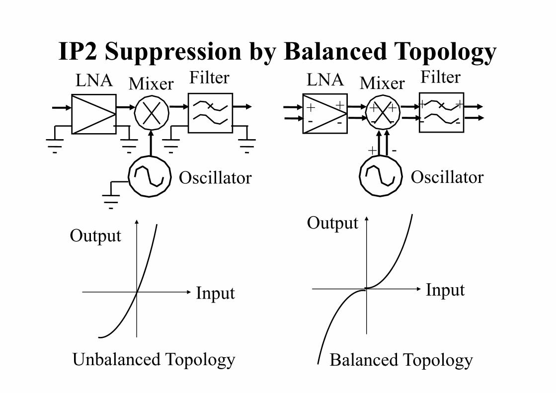
IP2 Suppression by Balanced Topology
Input
Output
Unbalanced Topology
Input
Output
LNA FilterMixer
Oscillator
Balanced Topology
LNA FilterMixer
Oscillator
+-
+-
+-
+-
+-
+-
+ -
•Noise Figures and Non-Linearities•RF Amplifier•Low Noise Amplifier Design Example
Contents
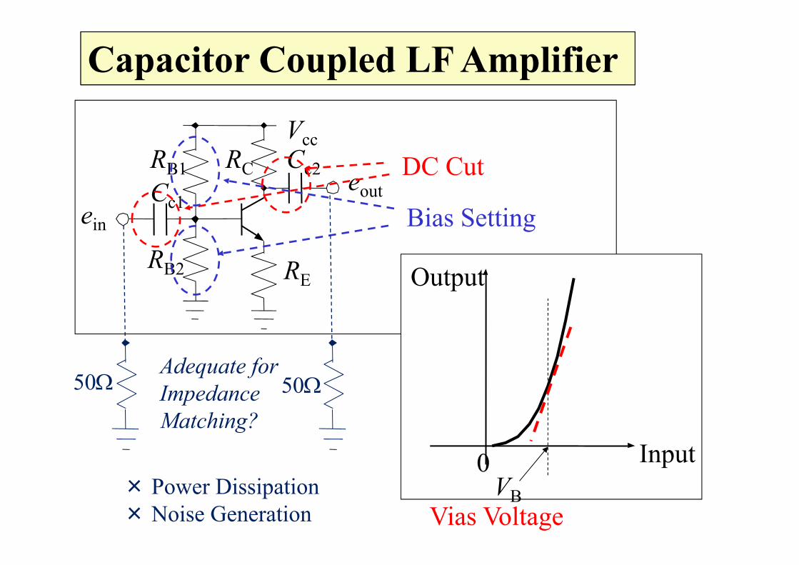
Capacitor Coupled LF Amplifier
VB
Input
Output
0
eout
RE
RB1
RB2
Cc1
RC
ein
Cc2 DC Cut
Bias Setting
Vias Voltage
Vcc
50 50Adequate for Impedance Matching?
× Power Dissipation× Noise Generation
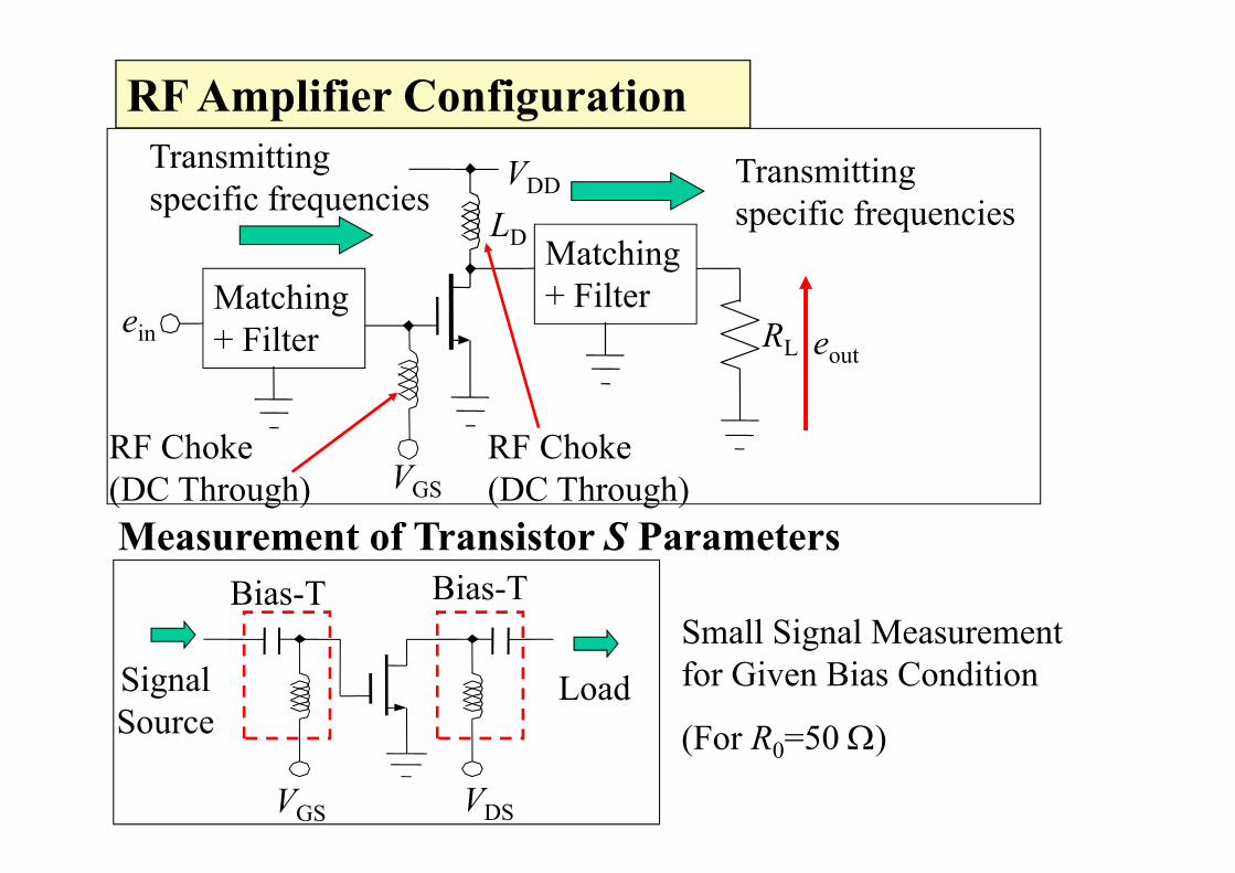
RF Amplifier Configuration
LD
RL
VDD
einMatching + Filter eout
Transmitting specific frequencies
Matching + Filter
RF Choke(DC Through)
RF Choke (DC Through)VGS
Transmitting specific frequencies
VGS VDS
Bias-TMeasurement of Transistor S Parameters
Small Signal Measurement for Given Bias Condition
(For R0=50 )
Signal Source
Load
Bias-T
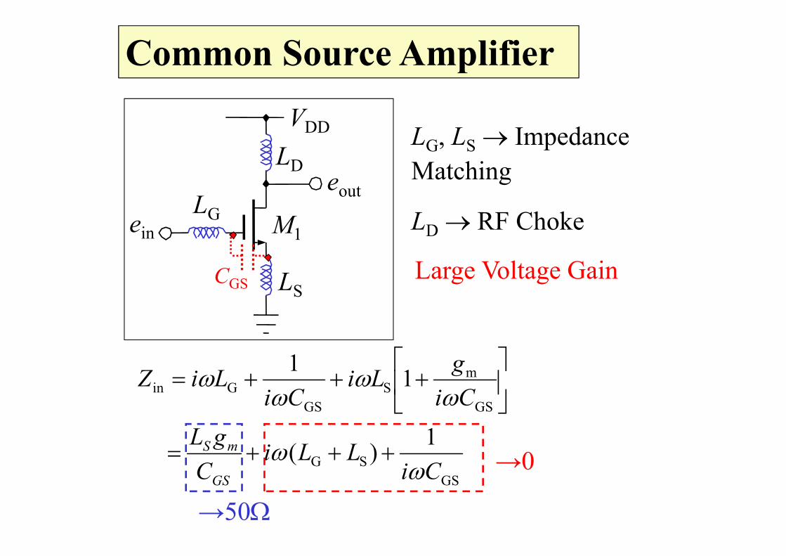
LS
M1
LD
LG
VDD
eout
ein
CGS
GSSG
GS
mS
GSGin
1)(
11
CiLLi
CgL
CigLi
CiLiZ
GS
mS
LG, LS Impedance Matching
LD RF Choke
Common Source Amplifier
Large Voltage Gain
→0
→50
vn- +
in -+
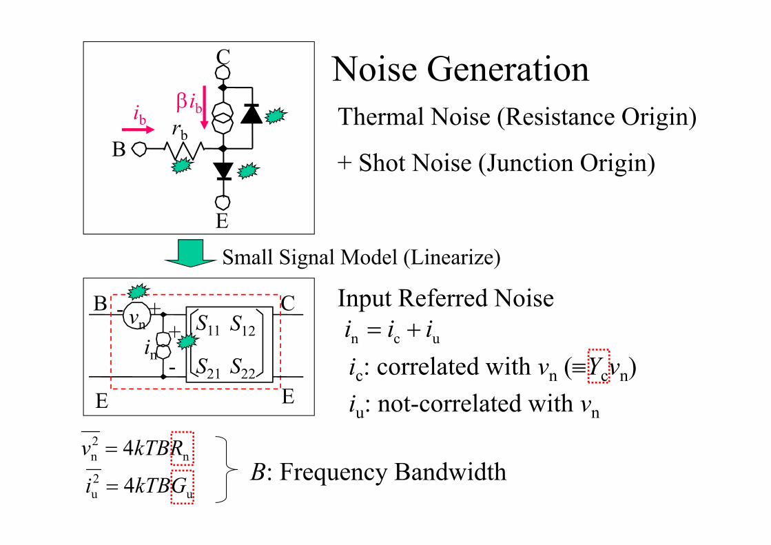
CB
EE
S11 S12
S21 S22
rb
ibib
B
C
E
Noise GenerationThermal Noise (Resistance Origin)
+ Shot Noise (Junction Origin)
Small Signal Model (Linearize)
Input Referred Noise
n2n 4kTBRv
u2u 4kTBGi
ucn iii ic: correlated with vn (Ycvn)iu: not-correlated with vn
B: Frequency Bandwidth
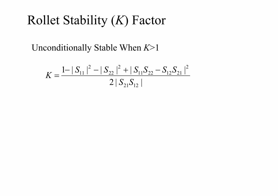
Rollet Stability (K) Factor
Unconditionally Stable When K>1
||2||||||1
1221
221122211
222
211
SSSSSSSSK
1.0
0.5
0.2
0.0
2 5 10
0.2
-0.2
0.5
1.0
2
5
10
-10
-5
-2
-1.0
-0.5
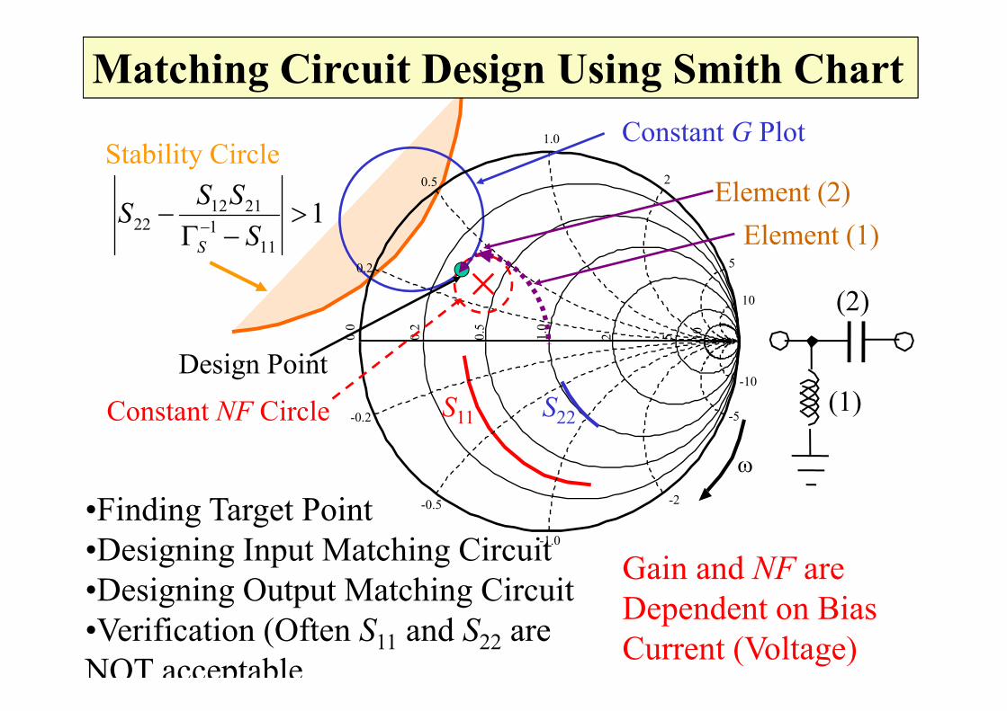
Constant G Plot
Constant NF Circle S11 S22
Element (1)Element (2)
Stability Circle
Matching Circuit Design Using Smith Chart
(1)
(2)
111
12112
22
SSSS
S
Design Point
•Finding Target Point•Designing Input Matching Circuit•Designing Output Matching Circuit•Verification (Often S11 and S22 are NOT acceptable
Gain and NF are Dependent on Bias Current (Voltage)
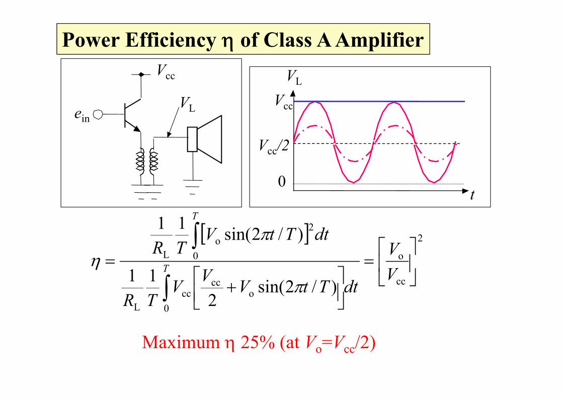
Power Efficiency of Class A AmplifierVcc
VLein
t
Vcc
0
VL
Vcc/2
2
cc
o
0o
cccc
L
0
2o
L
)/2sin(2
11
)/2sin(11
VV
dtTtVVVTR
dtTtVTR
T
T
Maximum 25% (at Vo=Vcc/2)
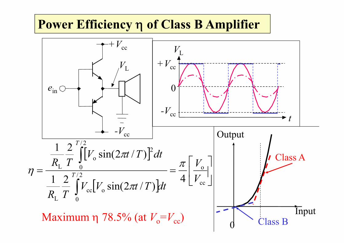
VL
ein
+Vcc
-Vcc
t
VL
+Vcc
-Vcc
0
Class A
Input
Output
0 Class B
cc
o2/
0occ
L
2/
0
2o
L
4)/2sin(21
)/2sin(21
VV
dtTtVVTR
dtTtVTR
T
T
Power Efficiency of Class B Amplifier
Maximum 78.5% (at Vo=Vcc)
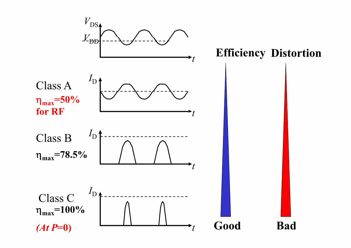
VDS
t
t
t
t
ID
ID
ID
VDD
Class A
Class B
Class C
Efficiency Distortion
Good Bad
max=50% for RF
max=78.5%
max=100%
(At P=0)
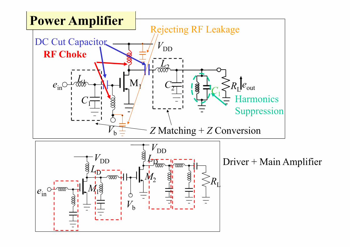
Power Amplifier
VDD
M1L1 eoutRLC1 Harmonics
Suppression
ein
Vb
L2
C2
C1
RF Choke
Rejecting RF LeakageDC Cut Capacitor
VDD
M1
M2
LDLD
RLein
Vb
VDD
Driver + Main Amplifier
Z Matching + Z Conversion
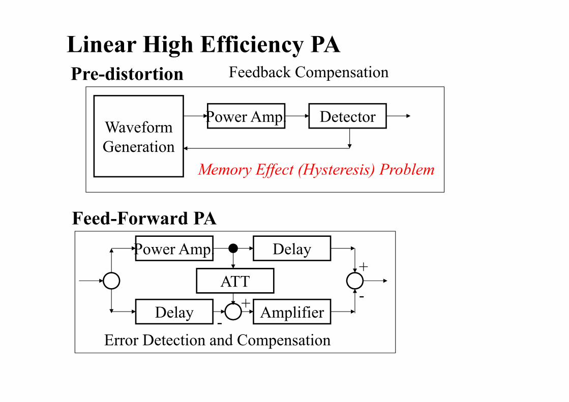
Pre-distortion
DetectorPower Amp.WaveformGeneration
Linear High Efficiency PAFeedback Compensation
Memory Effect (Hysteresis) Problem
-+
Error Detection and Compensation
Feed-Forward PAPower Amp.
Delay
ATT
Amplifier
Delay+
-
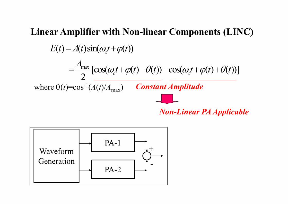
Linear Amplifier with Non-linear Components (LINC)
where (t)=cos-1(A(t)/Amax) Constant Amplitude
Non-Linear PA Applicable
max
( ) ( )sin( ( ))
[cos( ( ) ( )) cos( ( ) ( ))]2
c
c c
E t A t t tA t t t t t t
+
PA-2
PA-1
-WaveformGeneration
•Noise Figures and Non-Linearities•RF Amplifiers•Low Noise Amplifier Design Example
Contents
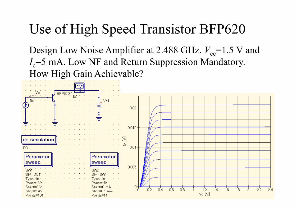
Use of High Speed Transistor BFP620Design Low Noise Amplifier at 2.488 GHz. Vcc=1.5 V and Ic=5 mA. Low NF and Return Suppression Mandatory. How High Gain Achievable?
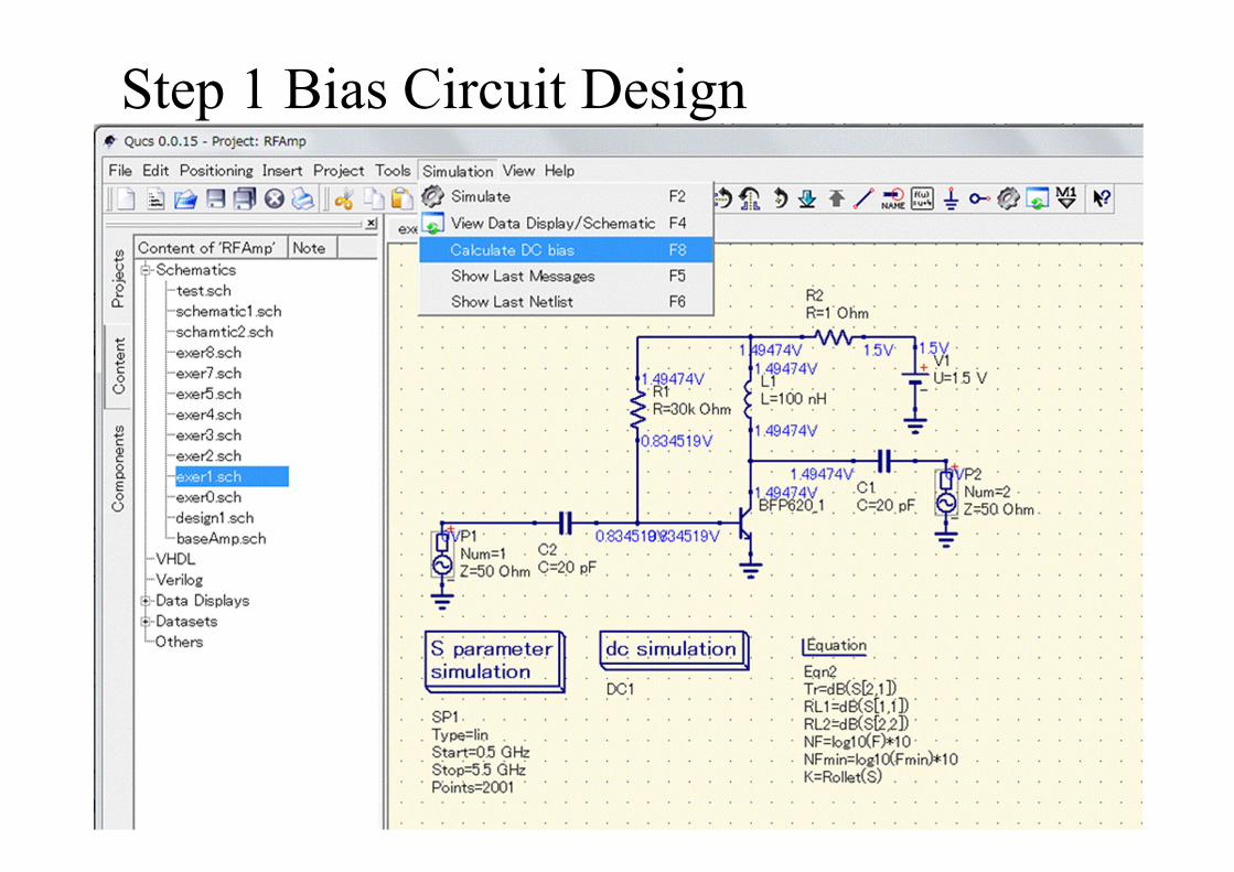
Step 1 Bias Circuit Design
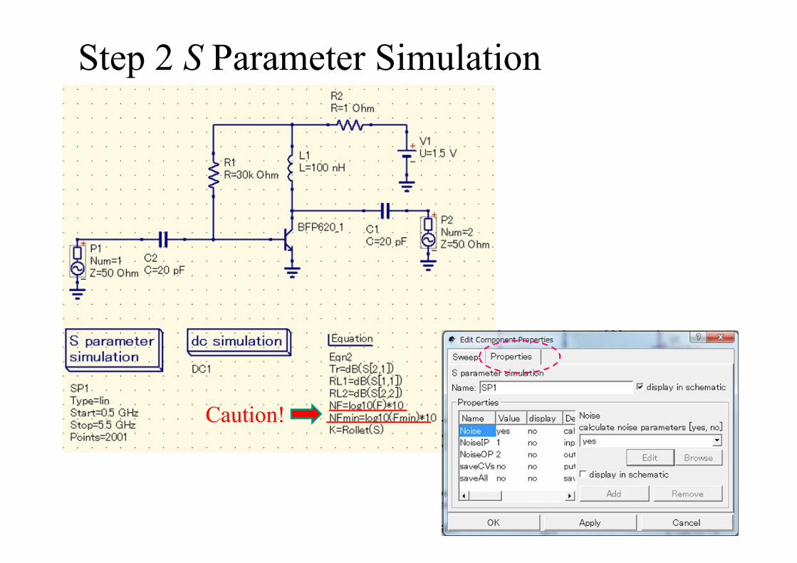
Step 2 S Parameter Simulation
Caution!
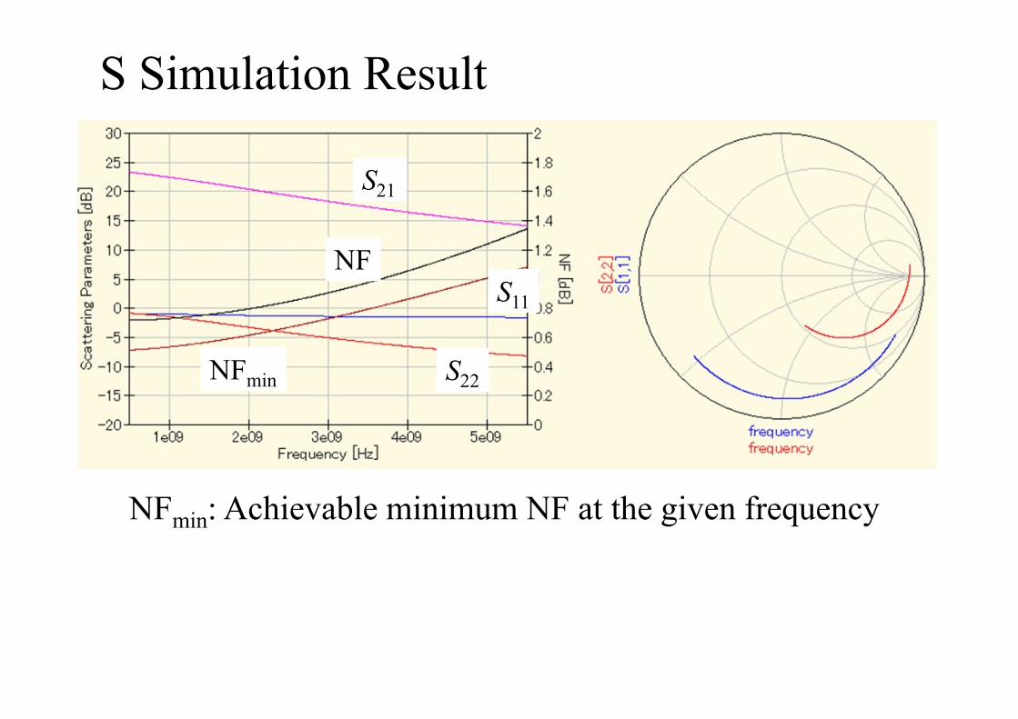
S Simulation Result
S21
S22
S11
NF
NFmin
NFmin: Achievable minimum NF at the given frequency
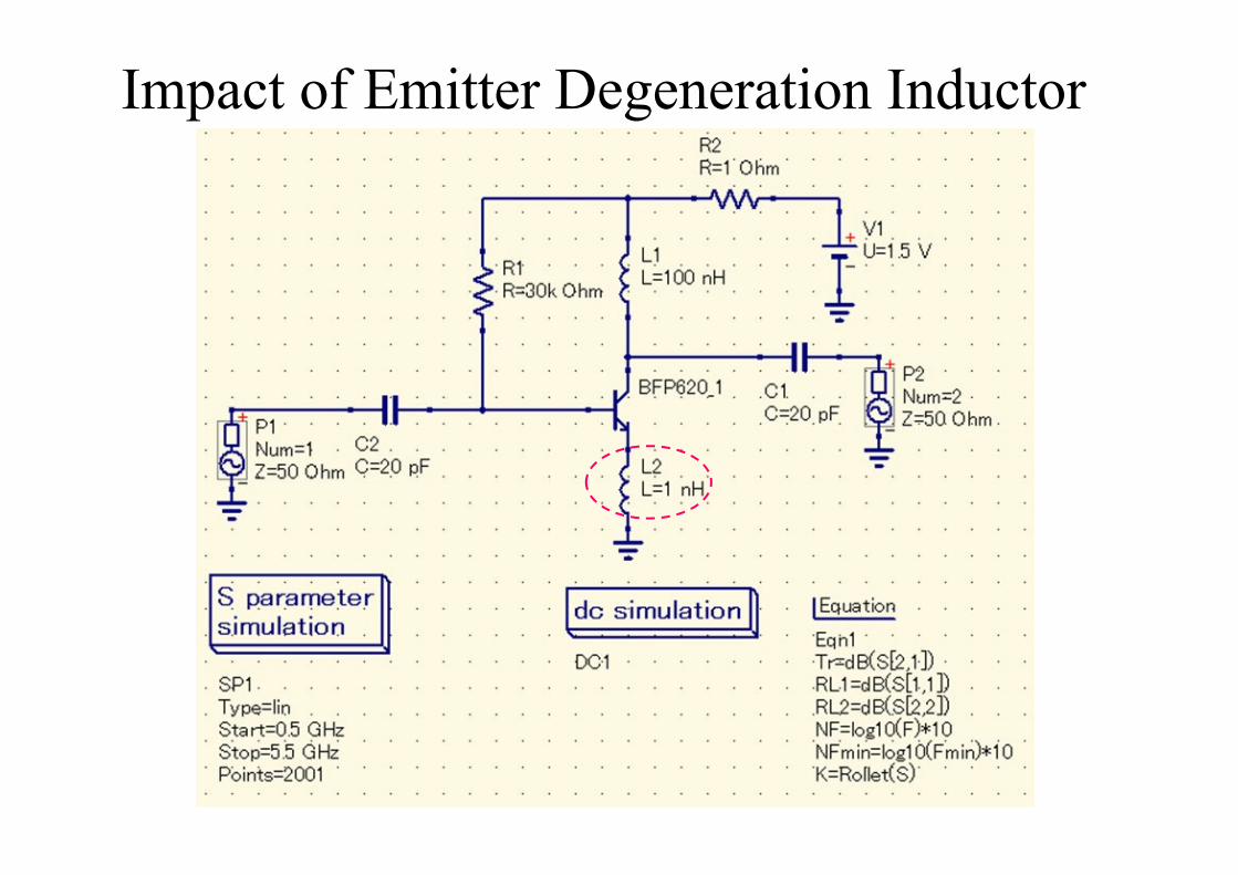
Impact of Emitter Degeneration Inductor
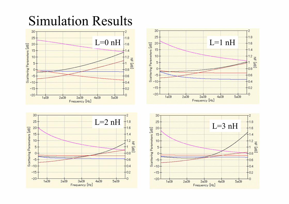
Simulation ResultsL=0 nH L=1 nH
L=2 nH L=3 nH
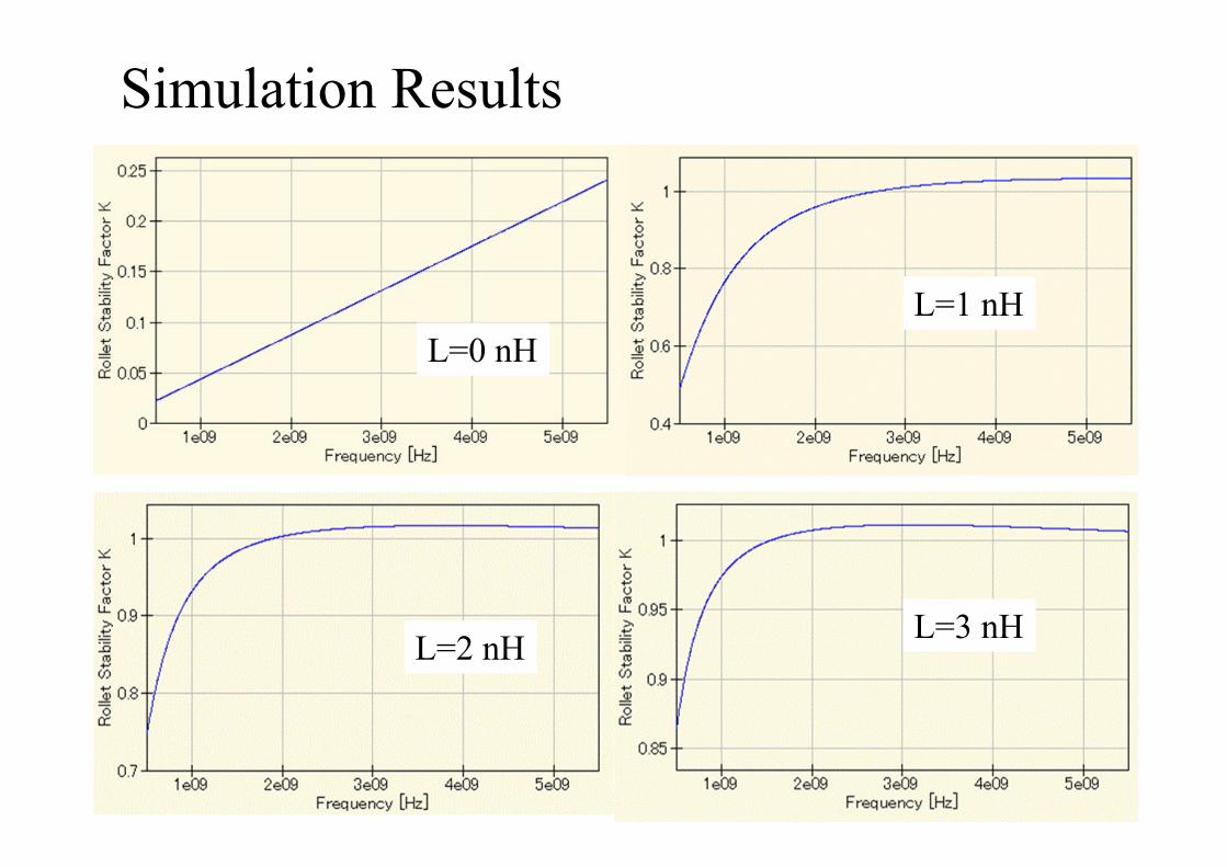
Simulation Results
L=0 nHL=1 nH
L=2 nH L=3 nH
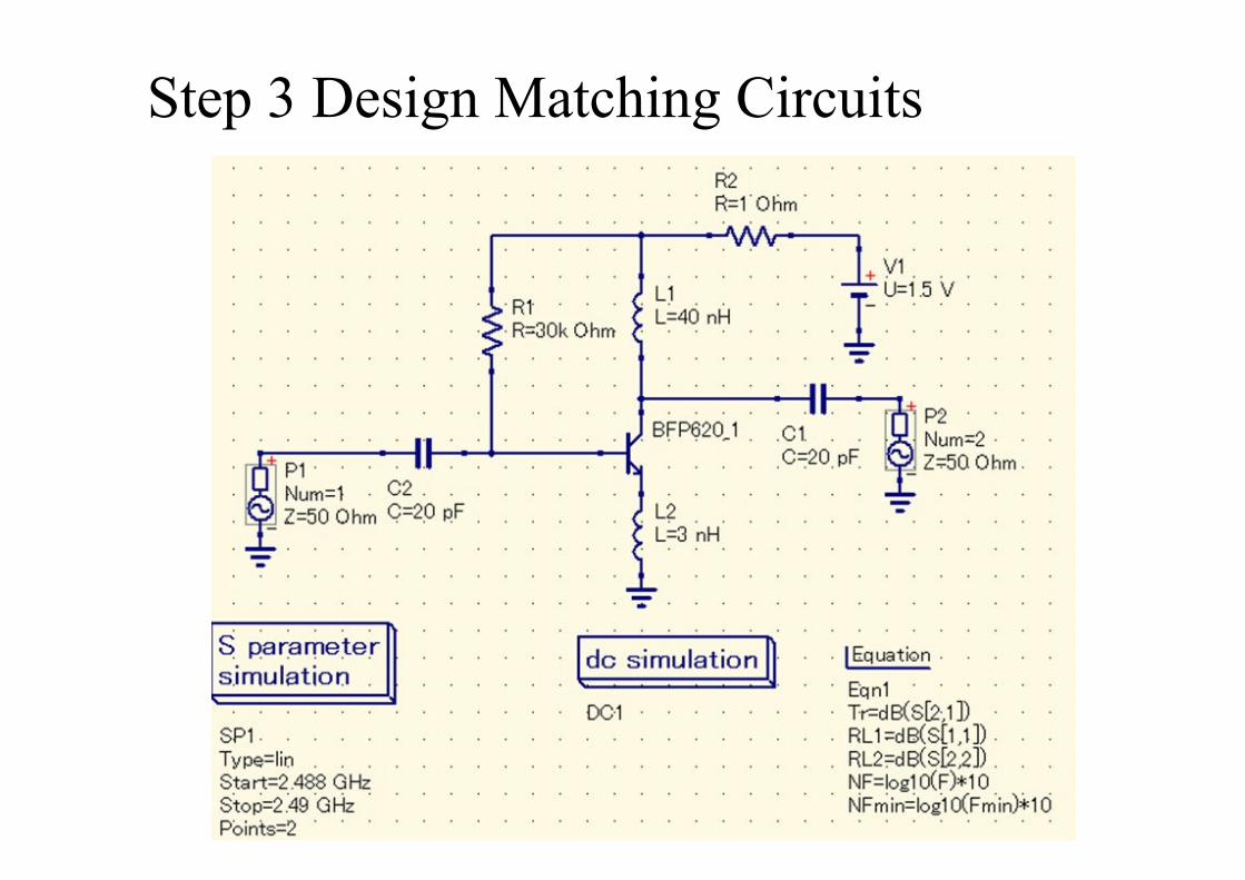
Step 3 Design Matching Circuits
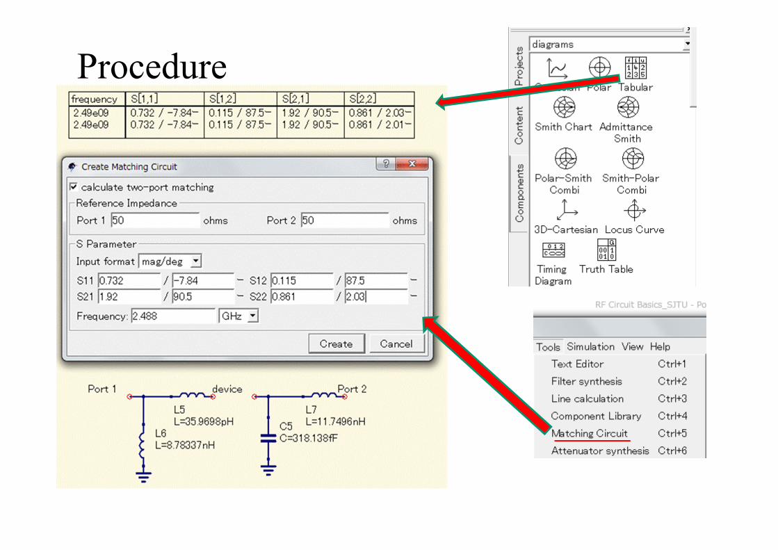
Procedure
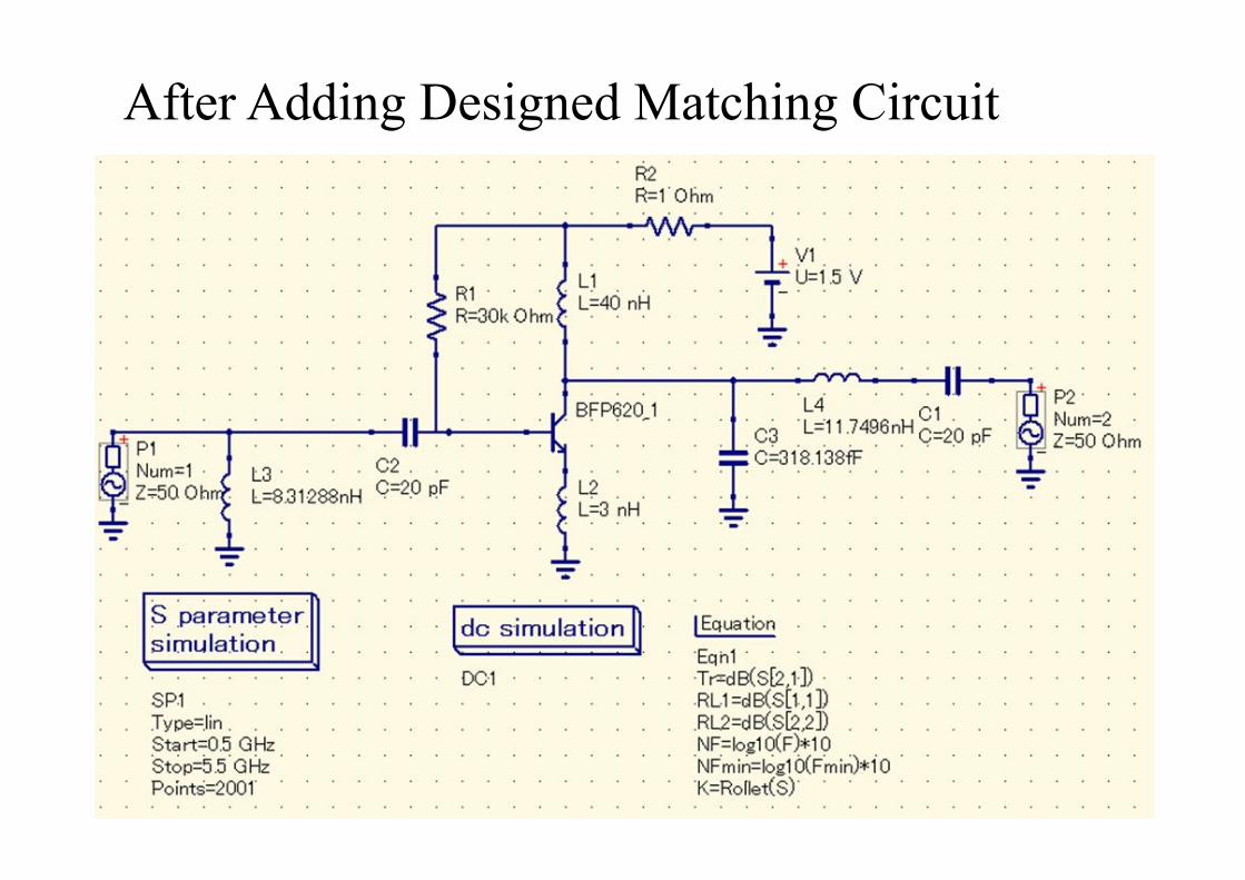
After Adding Designed Matching Circuit
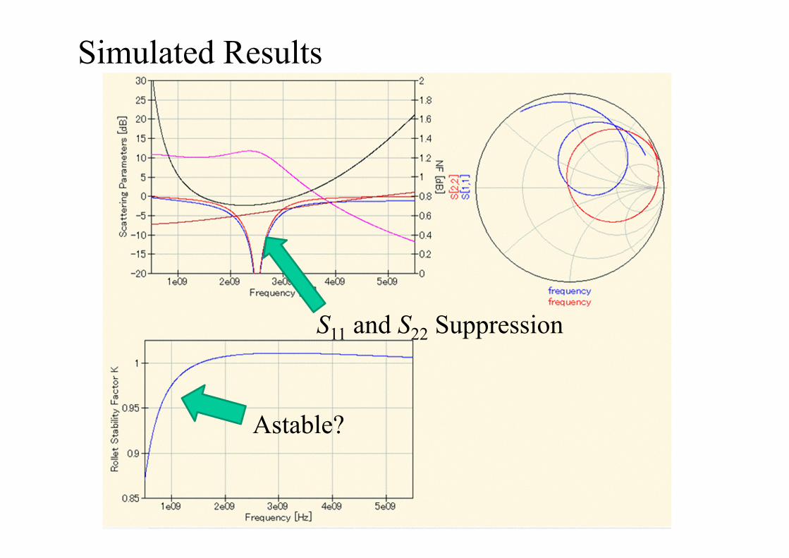
Simulated Results
S11 and S22 Suppression
Astable?
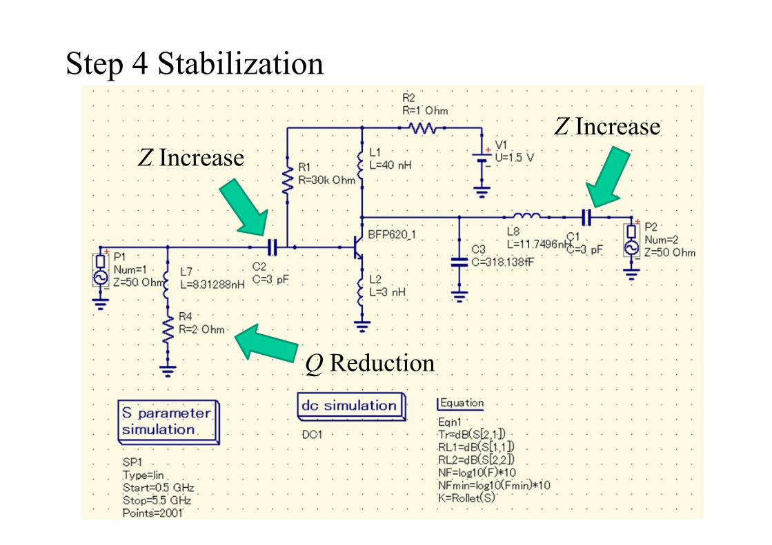
Q Reduction
Step 4 Stabilization
Z IncreaseZ Increase
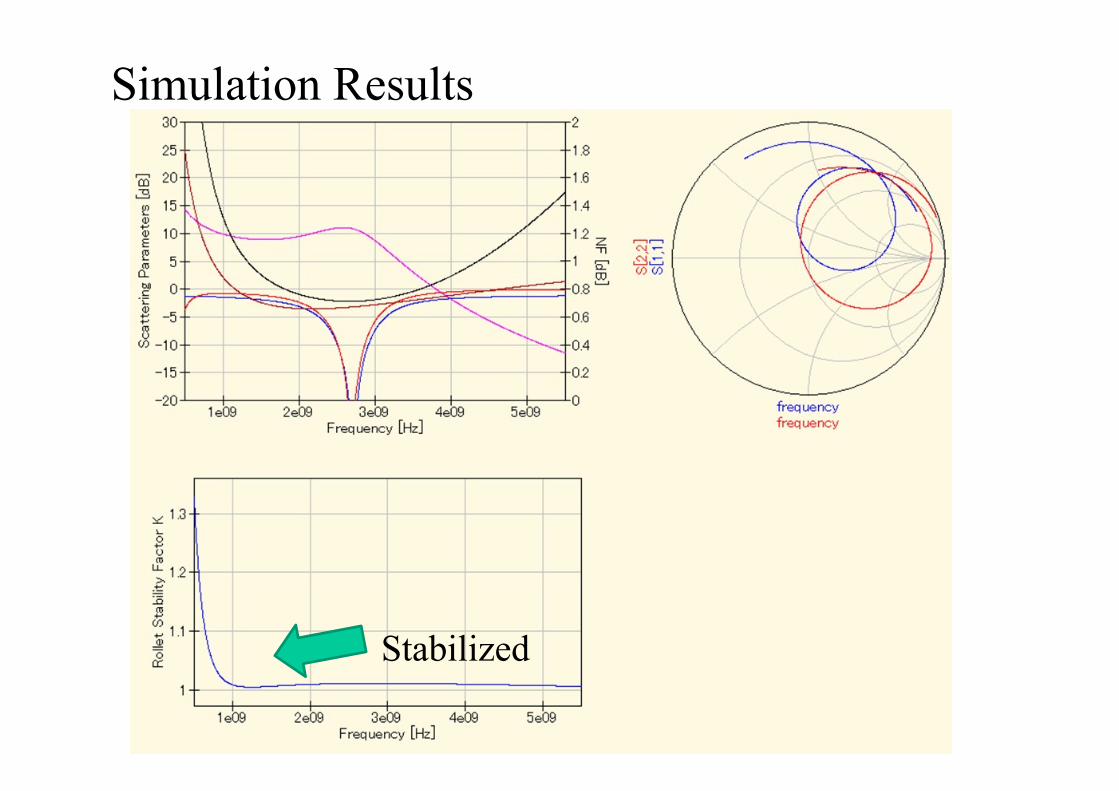
Stabilized
Simulation Results
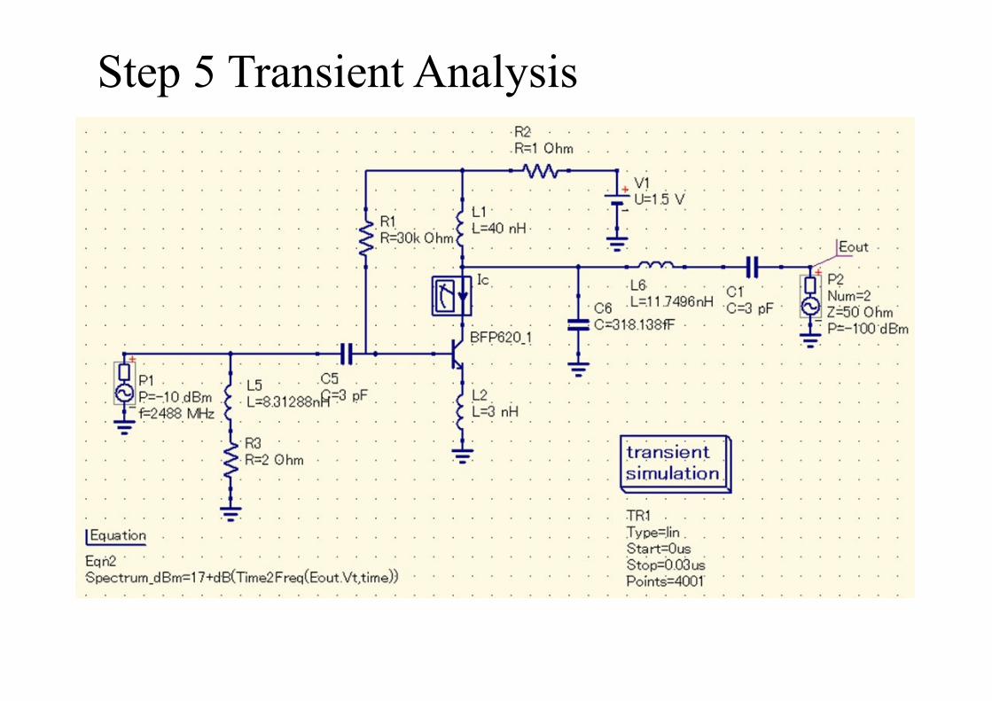
Step 5 Transient Analysis
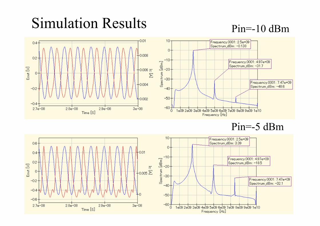
Simulation Results Pin=-10 dBm
Pin=-5 dBm
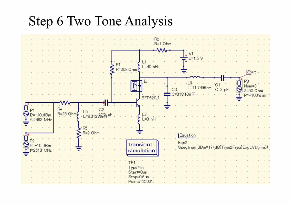
Step 6 Two Tone Analysis
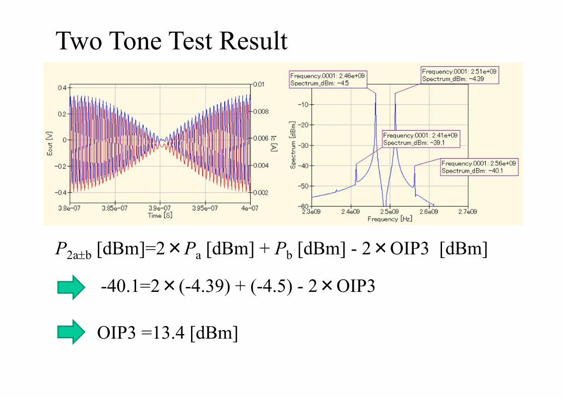
Two Tone Test Result
P2ab [dBm]=2×Pa [dBm] + Pb [dBm] - 2×OIP3 [dBm]
-40.1=2×(-4.39) + (-4.5) - 2×OIP3
OIP3 =13.4 [dBm]