Embed Size (px)
Citation preview

053-6021 APT100S20BG Datasheet Revision D 1
APT100S20BG High-Voltage Schottky Diode
1 Product OverviewThis section outlines the product overview for the APT100S20BG device.
1.1 FeaturesThe following are key features of the APT100S20BG device:
Low forward voltageLow leakage currentUltrafast reverse recoveryAvalanche energy ratedRoHS compliant
1.2 BenefitsThe following are benefits of the APT100S20BG device:
High switching frequencyLow switching lossesLow noise (EMI) switchingHigher reliability systemsIncreased system power density
1.3 ApplicationsThe APT100S20BG device is designed for the following applications:
Power supply and distributionSwitch-mode power supplyInverter, converter, and industrial motor driversHigh-speed rectifiers

053-6021 APT100S20BG Datasheet Revision D 2
2 Device SpecificationsThis section shows the device specifications for the APT100S20BG device.
2.1 Absolute Maximum RatingsThe following table shows the absolute maximum ratings for the APT100S20BG device. T = 25 °C unless J
otherwise specified.
Table 1 • Absolute Maximum Ratings
Symbol Parameter Ratings Unit
VR Maximum DC reverse voltage 200 V
VRRM Maximum peak repetitive reverse voltage
VRWM Maximum working peak reverse voltage
IF(AV) Maximum average forward current (T = 125 °C, duty cycle = 0.5)C 120 A
IF(RMS) RMS forward current 318
IFSM Non-repetitive forward surge current (T = 45 °C, 8.3 ms)J 1000
T , TJ STG Operating and storage temperature range –55 to 150 °C
TL Lead temperature for 10 seconds 300
The following table shows the thermal and mechanical characteristics of the APT100S20BG device.
Table 2 • Thermal and Mechanical Characteristics
Symbol Characteristic/Test Conditions Min Typ Max Unit
RθJC Junction-to-case thermal resistance 0.18 °C/W
Wt Package weight 0.22 oz
6.2 g
Maximum mounting torque, 6-32 or M3 screw 10 lbf-in
1.1 N-m
2.2 Electrical PerformanceThe following table shows the static characteristics of the APT100S20BG device. T = 25 °C unless J
otherwise specified.
Table 3 • Static Characteristics
Symbol Characteristic Test Conditions Min Typ Max Unit
VF Forward voltage I = 100 AF 0.89 0.95V
I = 200 AF 1.06
I = 100 A, T = 125 °CF J 0.76
IRM Maximum reverse leakage current V = 200 VR 2 mA
V = 200 V, T = 125 °CR J 40
CJ Junction capacitance V = 200 VR 470 pF
The following table shows the dynamic characteristics of the APT100S20BG device.

053-6021 APT100S20BG Datasheet Revision D 3
The following table shows the dynamic characteristics of the APT100S20BG device.
Table 4 • Dynamic Characteristics
Symbol Characteristic Test Conditions Min Typ Max Unit
trr Reverse recovery time I = 100 AF
di /dt = –200 A/µsF
V = 133 VR
T = 25 °CJ
70 ns
Qrr Reverse recovery charge 230 nC
IRRM Maximum reverse recovery current 6 A
trr Reverse recovery time I = 100 AF
di /dt = –200 A/µsF
V = 133 VR
T = 125 °CJ
110 ns
Qrr Reverse recovery charge 690 nC
IRRM Maximum reverse recovery current 11 A
trr Reverse recovery time I = 100 AF
di /dt = –700 A/µsF
V = 133 VR
T = 125 °CJ
95 ns
Qrr Reverse recovery charge 1750 nC
IRRM Maximum reverse recovery current 32 A
2.3 Typical Performance CurvesThis section shows the typical performance curves for the APT100S20BG device.
Figure 1 • Maximum Transient Thermal Impedance
Figure 2 • Forward Current vs. Forward Voltage (V) Figure 3 • RRT vs. Current Rate of Change
053-6021 APT100S20BG Datasheet Revision D 4
Figure 2 • Forward Current vs. Forward Voltage (V) Figure 3 • RRT vs. Current Rate of Change
Figure 4 • Reverse Recovery Charge vs. Current Rate of Change
Figure 5 • Reverse Recovery Current vs. Current Rate of Change
Figure 6 • Dynamic Parameters vs. Junction Figure 7 • Maximum Average Forward Current vs. Case

053-6021 APT100S20BG Datasheet Revision D 5
Figure 6 • Dynamic Parameters vs. Junction Temperature
Figure 7 • Maximum Average Forward Current vs. Case Temperature
Figure 8 • Junction Capacitance vs. Reverse Voltage Figure 9 • Single Pulse UIS SOA
053-6021 APT100S20BG Datasheet Revision D 6
1. 2. 3. 4.
5.
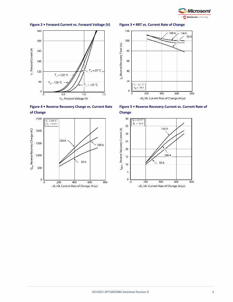
2.4 Reverse Recovery OverviewThe following illustration shows the diode test circuit for the APT100S20BG device.
Figure 10 • Diode Test Circuit
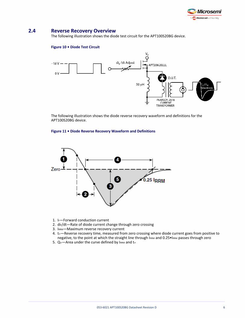
The following illustration shows the diode reverse recovery waveform and definitions for the APT100S20BG device.
Figure 11 • Diode Reverse Recovery Waveform and Definitions
I —Forward conduction currentF
di /dt—Rate of diode current change through zero crossingF
I —Maximum reverse recovery currentRRM
t —Reverse recovery time, measured from zero crossing where diode current goes from positive to rr
negative, to the point at which the straight line through I and 0.25•I passes through zeroRRM RRM
Q —Area under the curve defined by I and trr RRM rr

053-6021 APT100S20BG Datasheet Revision D 7
3 Package SpecificationThis section outlines the package specification for the APT100S20BG device.
3.1 Package Outline DrawingThe following figure shows the package outline drawing of the APT100S20BG device. Dimensions are in millimeters and (inches).
Figure 12 • Package Outline Drawing

053-6021 APT100S20BG Datasheet Revision D 8
Microsemi HeadquartersOne Enterprise, Aliso Viejo,CA 92656 USAWithin the USA: +1 (800) 713-4113Outside the USA: +1 (949) 380-6100Sales: +1 (949) 380-6136Fax: +1 (949) 215-4996Email: [email protected]
© 2019 Microsemi. All rights reserved. Microsemi and the Microsemi logo are trademarks of Microsemi Corporation. All other trademarks and service marks are the property of their respective owners.
Microsemi makes no warranty, representation, or guarantee regarding the information contained herein or the suitability of its products and services for any particular purpose, nor does Microsemi assume any liability whatsoever arising out of the application or use of any product or circuit. The products sold hereunder and any other products sold by Microsemi have been subject to limited testing and should not be used in conjunction with mission-critical equipment or applications. Any performance specifications are believed to be reliable but are not verified, and Buyer must conduct and complete all performance and other testing of the products, alone and together with, or installed in, any end-products. Buyer shall not rely on any data and performance specifications or parameters provided by Microsemi. It is the Buyer's responsibility to independently determine suitability of any products and to test and verify the same. The information provided by Microsemi hereunder is provided "as is, where is" and with all faults, and the entire risk associated with such information is entirely with the Buyer. Microsemi does not grant, explicitly or implicitly, to any party any patent rights, licenses, or any other IP rights, whether with regard to such information itself or anything described by such information. Information provided in this document is proprietary to Microsemi, and Microsemi reserves the right to make any changes to the information in this document or to any products and services at any time without notice.
Microsemi, a wholly owned subsidiary of Microchip Technology Inc. (Nasdaq: MCHP), offers a comprehensive portfolio of semiconductor and system solutions for aerospace & defense, communications, data center and industrial markets. Products include high-performance and radiation-hardened analog mixed-signal integrated circuits, FPGAs, SoCs and ASICs; power management products; timing and synchronization devices and precise time solutions, setting the world's standard for time; voice processing devices; RF solutions; discrete components; enterprise storage and communication solutions; security technologies and scalable anti-tamper products; Ethernet solutions; Power-over-Ethernet ICs and midspans; as well as custom design capabilities and services. Microsemi is headquartered in Aliso Viejo, California, and has approximately 4,800 employees globally. Learn more at www.microsemi.com.
053-6021 | February 2019 | Final