Embed Size (px)
Citation preview
ARM® 720TRevision: r0p0
Datasheet
Copyright © 1997, 1998 ARM Limited. All rights reserved.DDI 0087E
ARM 720TDatasheet
Copyright © 1997, 1998 ARM Limited. All rights reserved.
Release Information
The following changes have been made to this book.
Proprietary Notice
Words and logos marked with ® or ™ are registered trademarks or trademarks of ARM Limited in the EU and other countries, except as otherwise stated below in this proprietary notice. Other brands and names mentioned herein may be the trademarks of their respective owners.
Neither the whole nor any part of the information contained in, or the product described in, this document may be adapted or reproduced in any material form except with the prior written permission of the copyright holder.
The product described in this document is subject to continuous developments and improvements. All particulars of the product and its use contained in this document are given by ARM in good faith. However, all warranties implied or expressed, including but not limited to implied warranties of merchantability, or fitness for purpose, are excluded.
This document is intended only to assist the reader in the use of the product. ARM Limited shall not be liable for any loss or damage arising from the use of any information in this document, or any error or omission in such information, or any incorrect use of the product.
Where the term ARM is used it means “ARM or any of its subsidiaries as appropriate”.
Confidentiality Status
This document is Non-Confidential. The right to use, copy and disclose this document may be subject to license restrictions in accordance with the terms of the agreement entered into by ARM and the party that ARM delivered this document to.
Product Status
The information in this document is final, that is for a developed product.
Web Address
http://www.arm.com
Change History
Date Issue Change
Septempber 1997 B First draft of first release for r0p0
December 1997 C Update for next release
February 1998 D Change to Open Access
July 1998 E Logo, address changes, minor text changes
ii Copyright © 1997, 1998 ARM Limited. All rights reserved. DDI 0087E

ContentsARM 720T Datasheet
Chapter 1 Introduction1.1 Overview ..................................................................................................... 1-21.2 Block Diagram ............................................................................................. 1-31.3 Coprocessors .............................................................................................. 1-41.4 Instruction Set Overview ............................................................................. 1-5
Chapter 2 Signal Desriptions2.1 AMBA Interface Signals .............................................................................. 2-22.2 Coprocessor Interface Signals .................................................................... 2-42.3 JTAG Signals .............................................................................................. 2-62.4 Debugger Signals ....................................................................................... 2-72.5 Miscellaneous Signals ................................................................................ 2-8
Chapter 3 Programmers Model3.1 Processor Operating States ........................................................................ 3-23.2 Memory Formats ......................................................................................... 3-33.3 Instruction Length, Data Types, and Operating Modes ............................... 3-53.4 Registers ..................................................................................................... 3-63.5 The Program Status Registers .................................................................. 3-11
DDI 0087E Copyright © 1997, 1998 ARM Limited. All rights reserved. iii
Contents
3.6 Exceptions ................................................................................................ 3-143.7 Reset ........................................................................................................ 3-203.8 Relocation of Low Virtual Addresses by Process Identifier ...................... 3-213.9 Implementation-defined Behaviour of Instructions ................................... 3-22
Chapter 4 Configuration4.1 Overview ..................................................................................................... 4-24.2 Internal Coprocessor Instructions ............................................................... 4-44.3 Registers .................................................................................................... 4-5
Chapter 5 Instruction and Data Cache (IDC)5.1 Overview of the Instruction and Data Cache .............................................. 5-25.2 IDC Validity ................................................................................................. 5-45.3 IDC Enable/Disable and Reset ................................................................... 5-5
Chapter 6 Write Buffer6.1 Overview ..................................................................................................... 6-26.2 Write Buffer Operation ................................................................................ 6-3
Chapter 7 Memory Management Unit (MMU)7.1 Overview ..................................................................................................... 7-27.2 MMU Program Accessible Registers .......................................................... 7-47.3 Address Translation Process ...................................................................... 7-57.4 Level 1 Descriptor ....................................................................................... 7-77.5 Page Table Descriptor ................................................................................ 7-87.6 Section Descriptor ...................................................................................... 7-97.7 Translating Section References ............................................................... 7-117.8 Level 2 Descriptor ..................................................................................... 7-127.9 Translating Small Page References ......................................................... 7-147.10 Translating Large Page References ......................................................... 7-167.11 MMU Faults and CPU Aborts ................................................................... 7-187.12 Fault Address and Fault Status Registers (FAR & FSR) .......................... 7-197.13 Domain Access Control ............................................................................ 7-217.14 Fault Checking Sequence ........................................................................ 7-227.15 External Aborts ......................................................................................... 7-257.16 Interaction of the MMU, IDC and Write Buffer .......................................... 7-26
Chapter 8 Debug Interface8.1 Overview ..................................................................................................... 8-28.2 Debug Systems .......................................................................................... 8-48.3 Entering Debug State ................................................................................. 8-68.4 Scan Chains and JTAG Interface ............................................................... 8-88.5 Reset ........................................................................................................ 8-118.6 Public Instructions .................................................................................... 8-128.7 Test Data Registers .................................................................................. 8-168.8 ARM7DMT Core Clocks ........................................................................... 8-25
iv Copyright © 1997, 1998 ARM Limited. All rights reserved. DDI 0087E

Contents
8.9 Determining the Core and System State ................................................... 8-278.10 The PC During Debug ............................................................................... 8-328.11 Priorities and Exceptions .......................................................................... 8-368.12 Scan Interface Timing ............................................................................... 8-37
Chapter 9 EmbeddedICE Macrocell9.1 Overview ..................................................................................................... 9-29.2 The Watchpoint Registers ........................................................................... 9-59.3 Programming Breakpoints ......................................................................... 9-109.4 Programming Watchpoints ........................................................................ 9-129.5 The Debug Control Register ..................................................................... 9-149.6 Debug Status Register .............................................................................. 9-169.7 Coupling Breakpoints and Watchpoints .................................................... 9-189.8 Debug Communications Channel ............................................................. 9-20
Chapter 10 Bus Clocking10.1 Introduction ............................................................................................... 10-210.2 Fastbus Extension .................................................................................... 10-310.3 Standard Mode ......................................................................................... 10-5
Chapter 11 AMBA Interface11.1 ASB Bus Interface Signals ........................................................................ 11-211.2 Cycle Types .............................................................................................. 11-311.3 Addressing Signals ................................................................................... 11-711.4 Memory Request Signals .......................................................................... 11-811.5 Data Signal Timing .................................................................................... 11-911.6 Slave Response Signals ......................................................................... 11-1011.7 Maximum Sequential Length .................................................................. 11-1311.8 Read-Lock-Write ..................................................................................... 11-1411.9 Big-Endian / Little-Endian Operation ....................................................... 11-1511.10 Multi-master Operation ............................................................................ 11-1811.11 Bus Master Handover ............................................................................. 11-2011.12 Default Bus Master ................................................................................. 11-23
Chapter 12 AMBA Test12.1 Slave Operation (Test mode) .................................................................... 12-212.2 ARM720T Test Mode ................................................................................ 12-412.3 ARM7DMT Core Test Mode ...................................................................... 12-612.4 RAM Test Mode ........................................................................................ 12-712.5 TAG Test Mode ......................................................................................... 12-812.6 MMU Test Mode ..................................................................................... 12-1012.7 Test Register Mapping ............................................................................ 12-12
DDI 0087E Copyright © 1997, 1998 ARM Limited. All rights reserved. v

Contents
vi Copyright © 1997, 1998 ARM Limited. All rights reserved. DDI 0087E
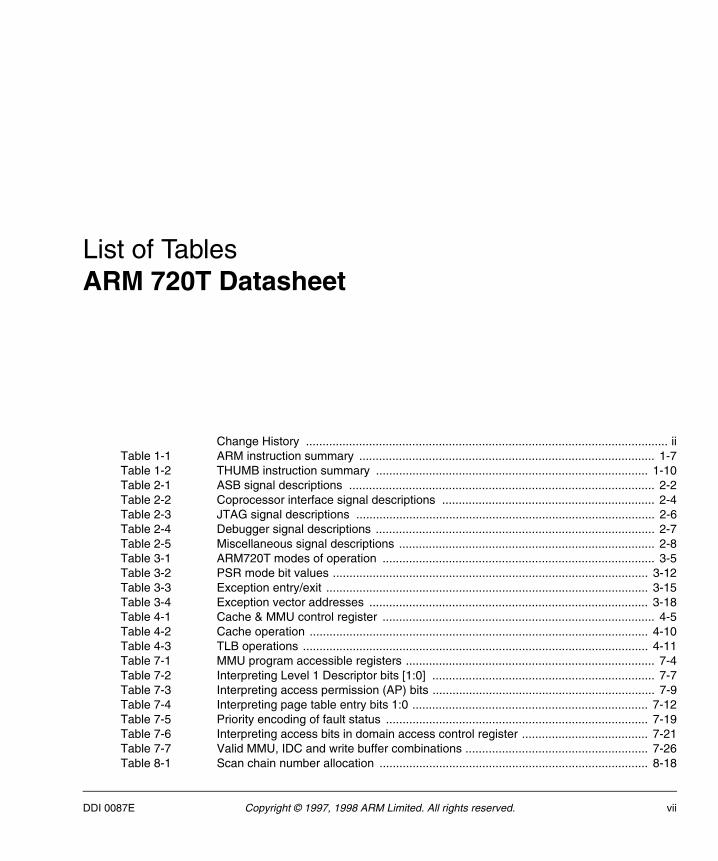
List of TablesARM 720T Datasheet
Change History ............................................................................................................. iiTable 1-1 ARM instruction summary ......................................................................................... 1-7Table 1-2 THUMB instruction summary .................................................................................. 1-10Table 2-1 ASB signal descriptions ............................................................................................ 2-2Table 2-2 Coprocessor interface signal descriptions ................................................................ 2-4Table 2-3 JTAG signal descriptions .......................................................................................... 2-6Table 2-4 Debugger signal descriptions .................................................................................... 2-7Table 2-5 Miscellaneous signal descriptions ............................................................................. 2-8Table 3-1 ARM720T modes of operation .................................................................................. 3-5Table 3-2 PSR mode bit values ............................................................................................... 3-12Table 3-3 Exception entry/exit ................................................................................................. 3-15Table 3-4 Exception vector addresses .................................................................................... 3-18Table 4-1 Cache & MMU control register .................................................................................. 4-5Table 4-2 Cache operation ...................................................................................................... 4-10Table 4-3 TLB operations ........................................................................................................ 4-11Table 7-1 MMU program accessible registers ........................................................................... 7-4Table 7-2 Interpreting Level 1 Descriptor bits [1:0] ................................................................... 7-7Table 7-3 Interpreting access permission (AP) bits ................................................................... 7-9Table 7-4 Interpreting page table entry bits 1:0 ....................................................................... 7-12Table 7-5 Priority encoding of fault status ............................................................................... 7-19Table 7-6 Interpreting access bits in domain access control register ...................................... 7-21Table 7-7 Valid MMU, IDC and write buffer combinations ....................................................... 7-26Table 8-1 Scan chain number allocation ................................................................................. 8-18
DDI 0087E Copyright © 1997, 1998 ARM Limited. All rights reserved. vii
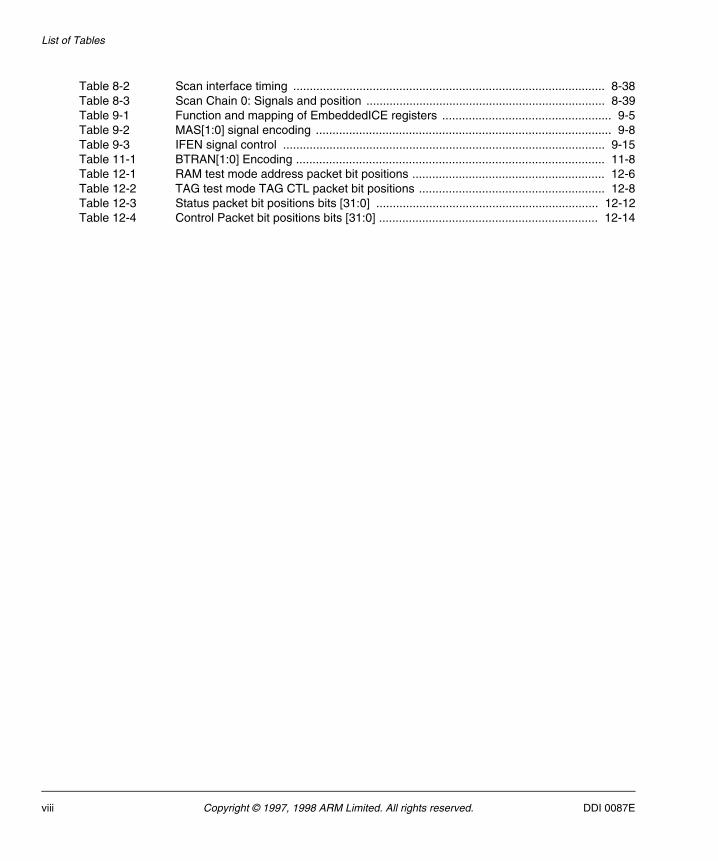
List of Tables
Table 8-2 Scan interface timing .............................................................................................. 8-38Table 8-3 Scan Chain 0: Signals and position ........................................................................ 8-39Table 9-1 Function and mapping of EmbeddedICE registers ................................................... 9-5Table 9-2 MAS[1:0] signal encoding ......................................................................................... 9-8Table 9-3 IFEN signal control ................................................................................................. 9-15Table 11-1 BTRAN[1:0] Encoding ............................................................................................. 11-8Table 12-1 RAM test mode address packet bit positions .......................................................... 12-6Table 12-2 TAG test mode TAG CTL packet bit positions ........................................................ 12-8Table 12-3 Status packet bit positions bits [31:0] ................................................................... 12-12Table 12-4 Control Packet bit positions bits [31:0] .................................................................. 12-14
viii Copyright © 1997, 1998 ARM Limited. All rights reserved. DDI 0087E

List of FiguresARM 720T Datasheet
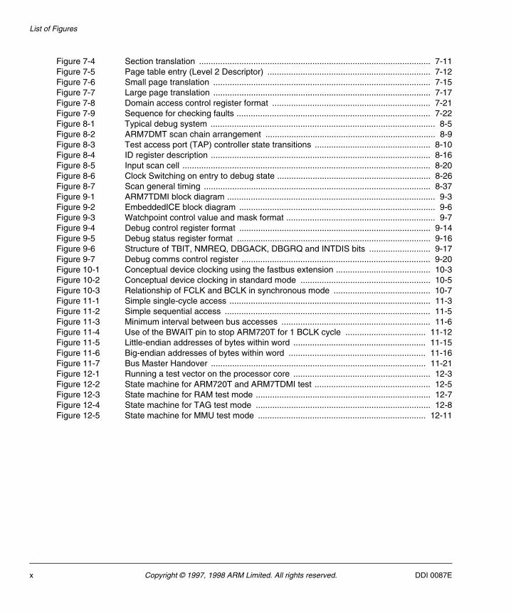
Figure 1-1 ARM720T block diagram ........................................................................................... 1-3Figure 1-2 ARM instruction set formats ...................................................................................... 1-6Figure 1-3 THUMB instruction set formats ................................................................................. 1-9Figure 3-1 Big-endian address of bytes within words ................................................................. 3-3Figure 3-2 Little-endian addresses of bytes with words ............................................................. 3-4Figure 3-3 Register organization in ARM state ........................................................................... 3-7Figure 3-4 Register organization in THUMB state ...................................................................... 3-8Figure 3-5 Mapping of THUMB state registers onto ARM state registers ................................. 3-10Figure 3-6 Program status register format ................................................................................ 3-11Figure 4-1 MRC, MCR bit pattern ............................................................................................... 4-4Figure 4-2 ID register read ......................................................................................................... 4-5Figure 4-3 ID register write ......................................................................................................... 4-6Figure 4-4 Register 1 read .......................................................................................................... 4-6Figure 4-5 Register 1 write ......................................................................................................... 4-6Figure 4-6 Register 2 .................................................................................................................. 4-8Figure 4-7 Register 3 .................................................................................................................. 4-8Figure 4-8 Register 4 .................................................................................................................. 4-9Figure 4-9 Register 5 ................................................................................................................ 4-10Figure 4-10 Register 6 ................................................................................................................ 4-10Figure 4-11 Register 13 .............................................................................................................. 4-11Figure 7-1 Translation table base register .................................................................................. 7-5Figure 7-2 Accessing the translation table first level descriptors ................................................ 7-6Figure 7-3 Level 1 Descriptors ................................................................................................... 7-7
DDI 0087E Copyright © 1997, 1998 ARM Limited. All rights reserved. ix
List of Figures
Figure 7-4 Section translation .................................................................................................. 7-11Figure 7-5 Page table entry (Level 2 Descriptor) ..................................................................... 7-12Figure 7-6 Small page translation ............................................................................................ 7-15Figure 7-7 Large page translation ............................................................................................ 7-17Figure 7-8 Domain access control register format ................................................................... 7-21Figure 7-9 Sequence for checking faults .................................................................................. 7-22Figure 8-1 Typical debug system ............................................................................................... 8-5Figure 8-2 ARM7DMT scan chain arrangement ........................................................................ 8-9Figure 8-3 Test access port (TAP) controller state transitions ................................................. 8-10Figure 8-4 ID register description ............................................................................................. 8-16Figure 8-5 Input scan cell ......................................................................................................... 8-20Figure 8-6 Clock Switching on entry to debug state ................................................................. 8-26Figure 8-7 Scan general timing ................................................................................................ 8-37Figure 9-1 ARM7TDMI block diagram ........................................................................................ 9-3Figure 9-2 EmbeddedICE block diagram ................................................................................... 9-6Figure 9-3 Watchpoint control value and mask format ............................................................... 9-7Figure 9-4 Debug control register format ................................................................................. 9-14Figure 9-5 Debug status register format .................................................................................. 9-16Figure 9-6 Structure of TBIT, NMREQ, DBGACK, DBGRQ and INTDIS bits .......................... 9-17Figure 9-7 Debug comms control register ................................................................................ 9-20Figure 10-1 Conceptual device clocking using the fastbus extension ........................................ 10-3Figure 10-2 Conceptual device clocking in standard mode ....................................................... 10-5Figure 10-3 Relationship of FCLK and BCLK in synchronous mode ......................................... 10-7Figure 11-1 Simple single-cycle access ..................................................................................... 11-3Figure 11-2 Simple sequential access ....................................................................................... 11-5Figure 11-3 Minimum interval between bus accesses ............................................................... 11-6Figure 11-4 Use of the BWAIT pin to stop ARM720T for 1 BCLK cycle .................................. 11-12Figure 11-5 Little-endian addresses of bytes within word ........................................................ 11-15Figure 11-6 Big-endian addresses of bytes within word .......................................................... 11-16Figure 11-7 Bus Master Handover ........................................................................................... 11-21Figure 12-1 Running a test vector on the processor core .......................................................... 12-3Figure 12-2 State machine for ARM720T and ARM7TDMI test ................................................. 12-5Figure 12-3 State machine for RAM test mode .......................................................................... 12-7Figure 12-4 State machine for TAG test mode .......................................................................... 12-8Figure 12-5 State machine for MMU test mode ....................................................................... 12-11
x Copyright © 1997, 1998 ARM Limited. All rights reserved. DDI 0087E
Chapter 1 Introduction
This chapter provides an introduction to the ARM720T.
• Overview on page 1-2
• Block Diagram on page 1-3
• Coprocessors on page 1-4
• Instruction Set Overview on page 1-5.
DDI 0087E Copyright © 1997, 1998 ARM Limited. All rights reserved. 1-1
Introduction
1.1 Overview
ARM720T is a general-purpose 32-bit microprocessor with 8KB cache, enlarged write buffer and Memory Management Unit (MMU) combined in a single chip. The CPU within ARM720T is the ARM7TDMI. The ARM720T is software compatible with the ARM processor family.
ARM720T is a fully static part and has been designed to minimize power requirements. This makes it ideal for portable applications, where both these features are essential.
The ARM720T architecture is based on Reduced Instruction Set Computer (RISC) principles, and the instruction set and related decode mechanism are greatly simplified compared with microprogrammed Complex Instruction Set Computers (CISC).
The on-chip mixed data and instruction cache, together with the write buffer, substantially raise the average execution speed and reduce the average amount of memory bandwidth required by the processor. This allows the external memory to support additional processors or Direct Memory Access (DMA) channels with minimal performance loss.
The allocation of virtual addresses with different task ID improves performance in task switching operations with the cache enabled. These relocated virtual addresses are monitored by the EmbeddedICE block.
The MMU supports a conventional two-level, page-table structure and a number of extensions which make it ideal for embedded control, UNIX and object-oriented systems.
The memory interface has been designed to allow the performance potential to be realized without incurring high costs in the memory system. Speed-critical control signals are pipelined to allow system control functions to be implemented in standard low-power logic, and these control signals permit the exploitation of paged mode access offered by industry standard DRAMs.
1-2 Copyright © 1997, 1998 ARM Limited. All rights reserved. DDI 0087E
Introduction
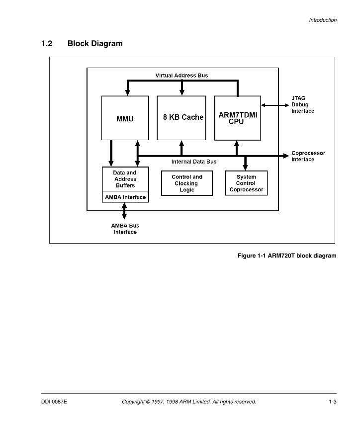
1.2 Block Diagram
Figure 1-1 ARM720T block diagram
DDI 0087E Copyright © 1997, 1998 ARM Limited. All rights reserved. 1-3
Introduction
1.3 Coprocessors
ARM720T still has an internal coprocessor designated #15 for internal control of the device. See Registers on page 4-5 for a complete description.
ARM720T also includes a port for the connection of on-chip coprocessors. These allow the functionality of the ARM720T to be extended in an architecturally consistent manner.
1-4 Copyright © 1997, 1998 ARM Limited. All rights reserved. DDI 0087E
Introduction
1.4 Instruction Set Overview
The instruction set comprises ten basic instruction types:
• Two of these make use of the on-chip arithmetic logic unit, barrel shifter and multiplier to perform high-speed operations on the data in a bank of 31 registers, each 32 bits wide.
• Three classes of instruction control the data transfer between memory and the registers:
— one optimized for flexibility of addressing
— one for rapid context switching
— one for swapping data
• Two instructions control the flow and privilege level of execution.
• Three types are dedicated to the control of external coprocessors which allow the functionality of the instruction set to be extended off-chip in an open and uniform way.
The ARM instruction set is a good target for compilers of many different high-level languages. Where required for critical code segments, assembly code programming is also straightforward, unlike some RISC processors which depend on sophisticated compiler technology to manage complicated instruction interdependencies.
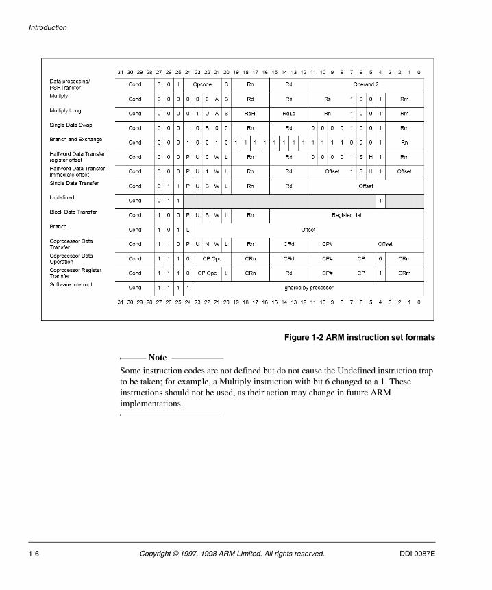
1.4.1 ARM instruction set
This section gives an overview of the ARM instructions available. For full details of these instructions, please refer to the ARM Architecture Reference Manual (ARM DDI 0100).
Format summary
The ARM instruction set formats are shown below.
DDI 0087E Copyright © 1997, 1998 ARM Limited. All rights reserved. 1-5
Introduction
Figure 1-2 ARM instruction set formats
Note Some instruction codes are not defined but do not cause the Undefined instruction trap to be taken; for example, a Multiply instruction with bit 6 changed to a 1. These instructions should not be used, as their action may change in future ARM implementations.
1-6 Copyright © 1997, 1998 ARM Limited. All rights reserved. DDI 0087E
Introduction
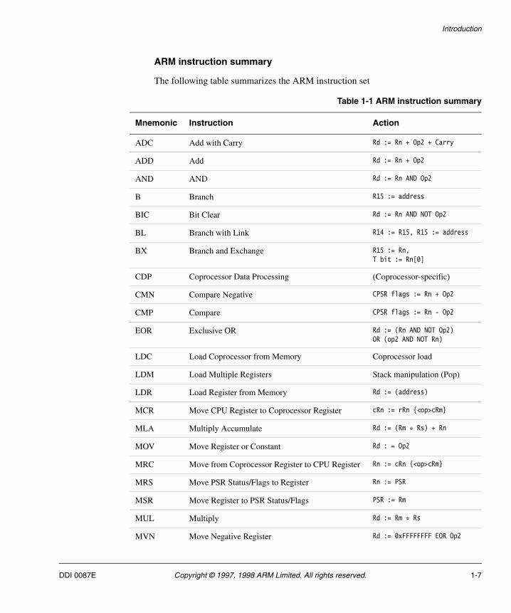
ARM instruction summary
The following table summarizes the ARM instruction set
Table 1-1 ARM instruction summary
Mnemonic Instruction Action
ADC Add with Carry Rd := Rn + Op2 + Carry
ADD Add Rd := Rn + Op2
AND AND Rd := Rn AND Op2
B Branch R15 := address
BIC Bit Clear Rd := Rn AND NOT Op2
BL Branch with Link R14 := R15, R15 := address
BX Branch and Exchange R15 := Rn,T bit := Rn[0]
CDP Coprocessor Data Processing (Coprocessor-specific)
CMN Compare Negative CPSR flags := Rn + Op2
CMP Compare CPSR flags := Rn - Op2
EOR Exclusive OR Rd := (Rn AND NOT Op2)OR (op2 AND NOT Rn)
LDC Load Coprocessor from Memory Coprocessor load
LDM Load Multiple Registers Stack manipulation (Pop)
LDR Load Register from Memory Rd := (address)
MCR Move CPU Register to Coprocessor Register cRn := rRn {<op>cRm}
MLA Multiply Accumulate Rd := (Rm * Rs) + Rn
MOV Move Register or Constant Rd : = Op2
MRC Move from Coprocessor Register to CPU Register Rn := cRn {<op>cRm}
MRS Move PSR Status/Flags to Register Rn := PSR
MSR Move Register to PSR Status/Flags PSR := Rm
MUL Multiply Rd := Rm * Rs
MVN Move Negative Register Rd := 0xFFFFFFFF EOR Op2
DDI 0087E Copyright © 1997, 1998 ARM Limited. All rights reserved. 1-7

Introduction
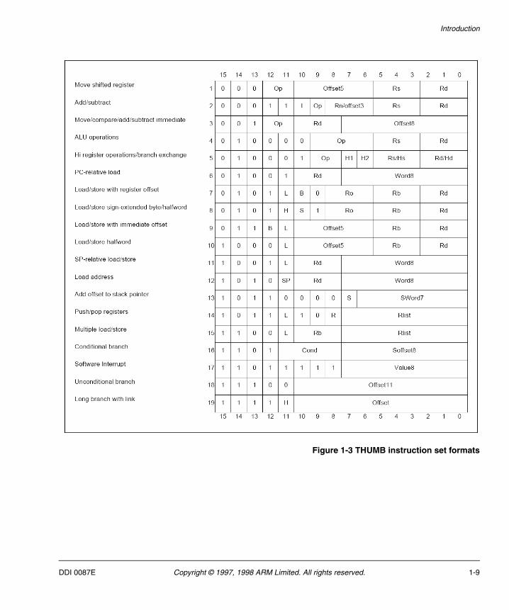
1.4.2 THUMB Instruction Set
This section gives an overview of the THUMB instructions available. For full details of these instructions, please refer to the ARM Architecture Reference Manual (ARM DDI 0100).
Format summary
The THUMB instruction set formats are shown in the following figure.
ORR OR Rd := Rn OR Op2
RSB Reverse Subtract Rd := Op2 - Rn
RSC Reverse Subtract with Carry Rd := Op2 - Rn - 1 + Carry
SBC Subtract with Carry Rd := Rn - Op2 - 1 + Carry
STC Store Coprocessor Register to Memory address := CRn
STM Store Multiple Stack manipulation (Push)
STR Store Register to Memory <address> := Rd
SUB Subtract Rd := Rn - Op2
SWI Software Interrupt OS call
SWP Swap Register with Memory Rd := [Rn], [Rn] := Rm
TEQ Test Bitwise Equality CPSR flags := Rn EOR Op2
TST Test Bits CPSR flags := Rn AND Op2
Table 1-1 ARM instruction summary (continued)
Mnemonic Instruction Action
1-8 Copyright © 1997, 1998 ARM Limited. All rights reserved. DDI 0087E
Introduction
Figure 1-3 THUMB instruction set formats
DDI 0087E Copyright © 1997, 1998 ARM Limited. All rights reserved. 1-9
Introduction
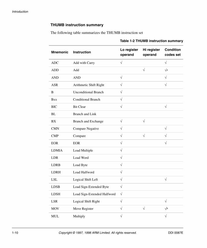
THUMB instruction summary
The following table summarizes the THUMB instruction set
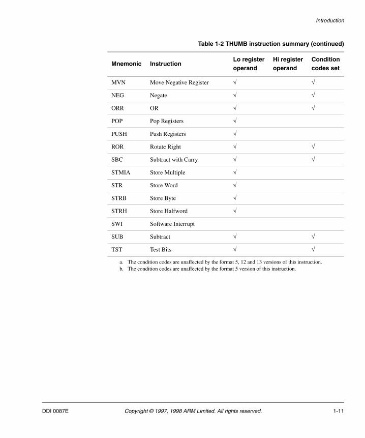
Table 1-2 THUMB instruction summary
Mnemonic InstructionLo registeroperand
Hi registeroperand
Conditioncodes set
ADC Add with Carry √ √
ADD Add √ √a
AND AND √ √
ASR Arithmetic Shift Right √ √
B Unconditional Branch √
Bxx Conditional Branch √
BIC Bit Clear √ √
BL Branch and Link
BX Branch and Exchange √ √
CMN Compare Negative √ √
CMP Compare √ √ √
EOR EOR √ √
LDMIA Load Multiple √
LDR Load Word √
LDRB Load Byte √
LDRH Load Halfword √
LSL Logical Shift Left √ √
LDSB Load Sign-Extended Byte √
LDSH Load Sign-Extended Halfword √
LSR Logical Shift Right √ √
MOV Move Register √ √ √b
MUL Multiply √ √
1-10 Copyright © 1997, 1998 ARM Limited. All rights reserved. DDI 0087E
Introduction
MVN Move Negative Register √ √
NEG Negate √ √
ORR OR √ √
POP Pop Registers √
PUSH Push Registers √
ROR Rotate Right √ √
SBC Subtract with Carry √ √
STMIA Store Multiple √
STR Store Word √
STRB Store Byte √
STRH Store Halfword √
SWI Software Interrupt
SUB Subtract √ √
TST Test Bits √ √
a. The condition codes are unaffected by the format 5, 12 and 13 versions of this instruction.b. The condition codes are unaffected by the format 5 version of this instruction.
Table 1-2 THUMB instruction summary (continued)
Mnemonic InstructionLo registeroperand
Hi registeroperand
Conditioncodes set
DDI 0087E Copyright © 1997, 1998 ARM Limited. All rights reserved. 1-11

Introduction
1-12 Copyright © 1997, 1998 ARM Limited. All rights reserved. DDI 0087E
Chapter 2 Signal Desriptions
This chapter describes the interface signals of ARM720T.
• AMBA Interface Signals on page 2-2
• Coprocessor Interface Signals on page 2-4
• JTAG Signals on page 2-6
• Debugger Signals on page 2-7
• Miscellaneous Signals on page 2-8.
DDI 0087E Copyright © 1997, 1998 ARM Limited. All rights reserved. 2-1
Signal Desriptions
2.1 AMBA Interface Signals
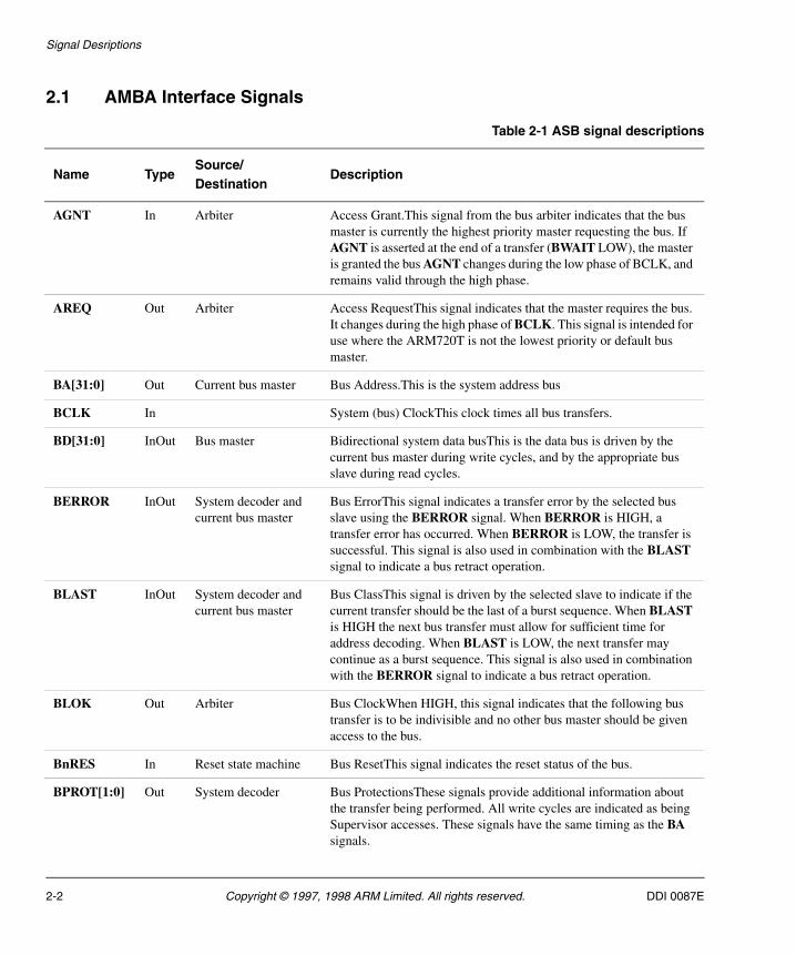
Table 2-1 ASB signal descriptions
Name TypeSource/Destination
Description
AGNT In Arbiter Access Grant.This signal from the bus arbiter indicates that the bus master is currently the highest priority master requesting the bus. If AGNT is asserted at the end of a transfer (BWAIT LOW), the master is granted the bus AGNT changes during the low phase of BCLK, and remains valid through the high phase.
AREQ Out Arbiter Access RequestThis signal indicates that the master requires the bus. It changes during the high phase of BCLK. This signal is intended for use where the ARM720T is not the lowest priority or default bus master.
BA[31:0] Out Current bus master Bus Address.This is the system address bus
BCLK In System (bus) ClockThis clock times all bus transfers.
BD[31:0] InOut Bus master Bidirectional system data busThis is the data bus is driven by the current bus master during write cycles, and by the appropriate bus slave during read cycles.
BERROR InOut System decoder and current bus master
Bus ErrorThis signal indicates a transfer error by the selected bus slave using the BERROR signal. When BERROR is HIGH, a transfer error has occurred. When BERROR is LOW, the transfer is successful. This signal is also used in combination with the BLAST signal to indicate a bus retract operation.
BLAST InOut System decoder and current bus master
Bus ClassThis signal is driven by the selected slave to indicate if the current transfer should be the last of a burst sequence. When BLAST is HIGH the next bus transfer must allow for sufficient time for address decoding. When BLAST is LOW, the next transfer may continue as a burst sequence. This signal is also used in combination with the BERROR signal to indicate a bus retract operation.
BLOK Out Arbiter Bus ClockWhen HIGH, this signal indicates that the following bus transfer is to be indivisible and no other bus master should be given access to the bus.
BnRES In Reset state machine Bus ResetThis signal indicates the reset status of the bus.
BPROT[1:0] Out System decoder Bus ProtectionsThese signals provide additional information about the transfer being performed. All write cycles are indicated as being Supervisor accesses. These signals have the same timing as the BA signals.
2-2 Copyright © 1997, 1998 ARM Limited. All rights reserved. DDI 0087E
Signal Desriptions
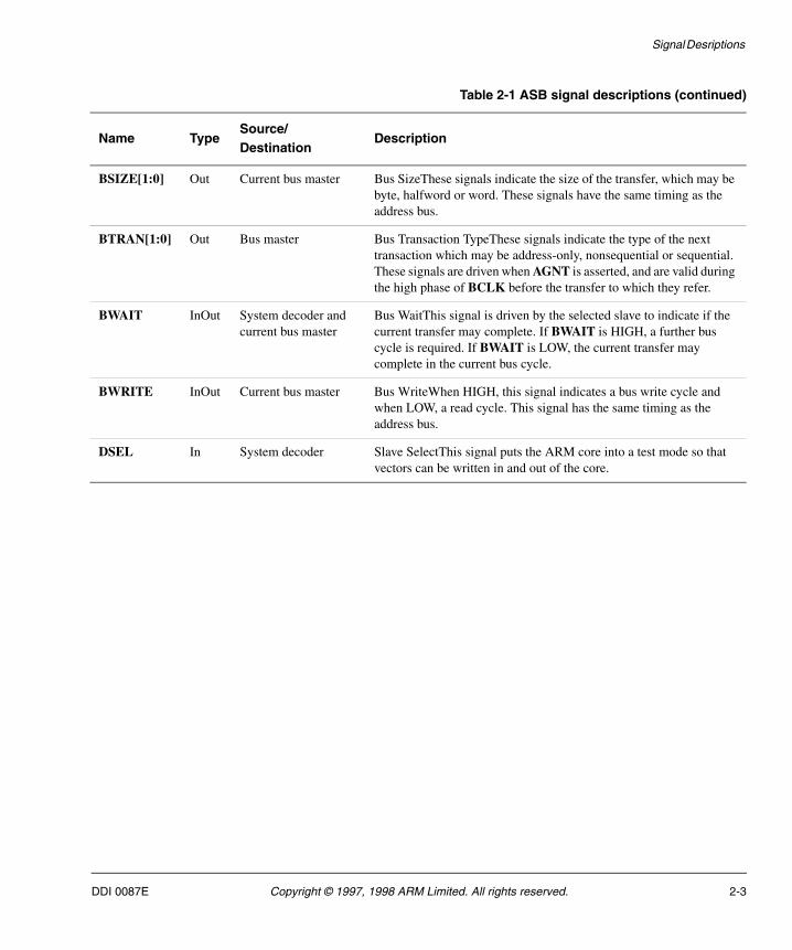
BSIZE[1:0] Out Current bus master Bus SizeThese signals indicate the size of the transfer, which may be byte, halfword or word. These signals have the same timing as the address bus.
BTRAN[1:0] Out Bus master Bus Transaction TypeThese signals indicate the type of the next transaction which may be address-only, nonsequential or sequential. These signals are driven when AGNT is asserted, and are valid during the high phase of BCLK before the transfer to which they refer.
BWAIT InOut System decoder and current bus master
Bus WaitThis signal is driven by the selected slave to indicate if the current transfer may complete. If BWAIT is HIGH, a further bus cycle is required. If BWAIT is LOW, the current transfer may complete in the current bus cycle.
BWRITE InOut Current bus master Bus WriteWhen HIGH, this signal indicates a bus write cycle and when LOW, a read cycle. This signal has the same timing as the address bus.
DSEL In System decoder Slave SelectThis signal puts the ARM core into a test mode so that vectors can be written in and out of the core.
Table 2-1 ASB signal descriptions (continued)
Name TypeSource/Destination
Description
DDI 0087E Copyright © 1997, 1998 ARM Limited. All rights reserved. 2-3
Signal Desriptions
2.2 Coprocessor Interface Signals
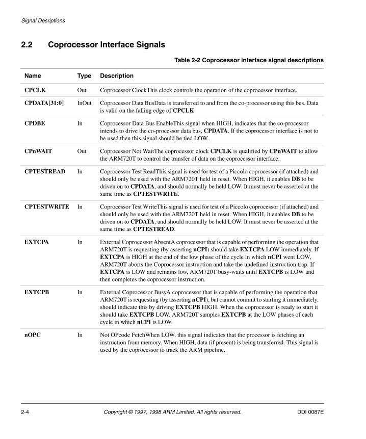
Table 2-2 Coprocessor interface signal descriptions
Name Type Description
CPCLK Out Coprocessor ClockThis clock controls the operation of the coprocessor interface.
CPDATA[31:0] InOut Coprocessor Data BusData is transferred to and from the co-processor using this bus. Data is valid on the falling edge of CPCLK.
CPDBE In Coprocessor Data Bus EnableThis signal when HIGH, indicates that the co-processor intends to drive the co-processor data bus, CPDATA. If the coprocessor interface is not to be used then this signal should be tied LOW.
CPnWAIT Out Coprocessor Not WaitThe coprocessor clock CPCLK is qualified by CPnWAIT to allow the ARM720T to control the transfer of data on the coprocessor interface.
CPTESTREAD In Coprocessor Test ReadThis signal is used for test of a Piccolo coprocessor (if attached) and should only be used with the ARM720T held in reset. When HIGH, it enables DB to be driven on to CPDATA, and should normally be held LOW. It must never be asserted at the same time as CPTESTWRITE.
CPTESTWRITE In Coprocessor Test WriteThis signal is used for test of a Piccolo coprocessor (if attached) and should only be used with the ARM720T held in reset. When HIGH, it enables DB to be driven on to CPDATA, and should normally be held LOW. It must never be asserted at the same time as CPTESTREAD.
EXTCPA In External Coprocessor AbsentA coprocessor that is capable of performing the operation that ARM720T is requesting (by asserting nCPI) should take EXTCPA LOW immediately. If EXTCPA is HIGH at the end of the low phase of the cycle in which nCPI went LOW, ARM720T aborts the Coprocessor instruction and take the undefined instruction trap. If EXTCPA is LOW and remains low, ARM720T busy-waits until EXTCPB is LOW and then completes the coprocessor instruction.
EXTCPB In External Coprocessor BusyA coprocessor that is capable of performing the operation that ARM720T is requesting (by asserting nCPI), but cannot commit to starting it immediately, should indicate this by driving EXTCPB HIGH. When the coprocessor is ready to start it should take EXTCPB LOW. ARM720T samples EXTCPB at the LOW phases of each cycle in which nCPI is LOW.
nOPC In Not OPcode FetchWhen LOW, this signal indicates that the processor is fetching an instruction from memory. When HIGH, data (if present) is being transferred. This signal is used by the coprocessor to track the ARM pipeline.
2-4 Copyright © 1997, 1998 ARM Limited. All rights reserved. DDI 0087E
Signal Desriptions
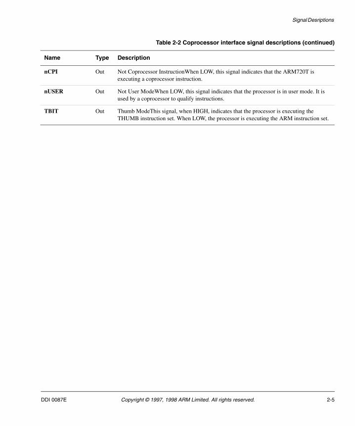
nCPI Out Not Coprocessor InstructionWhen LOW, this signal indicates that the ARM720T is executing a coprocessor instruction.
nUSER Out Not User ModeWhen LOW, this signal indicates that the processor is in user mode. It is used by a coprocessor to qualify instructions.
TBIT Out Thumb ModeThis signal, when HIGH, indicates that the processor is executing the THUMB instruction set. When LOW, the processor is executing the ARM instruction set.
Table 2-2 Coprocessor interface signal descriptions (continued)
Name Type Description
DDI 0087E Copyright © 1997, 1998 ARM Limited. All rights reserved. 2-5
Signal Desriptions
2.3 JTAG Signals
Table 2-3 JTAG signal descriptions
Name Type Description
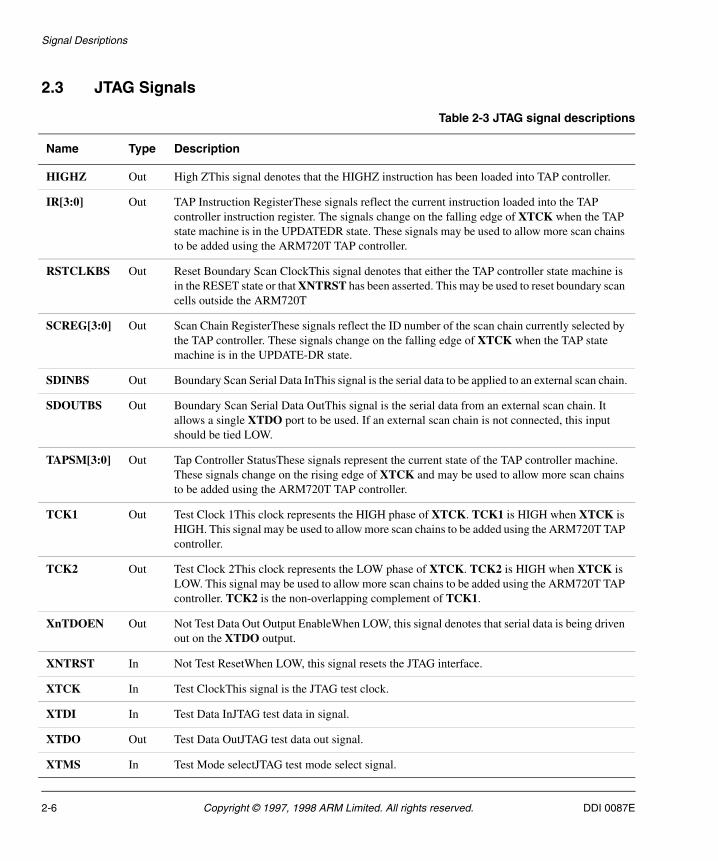
HIGHZ Out High ZThis signal denotes that the HIGHZ instruction has been loaded into TAP controller.
IR[3:0] Out TAP Instruction RegisterThese signals reflect the current instruction loaded into the TAP controller instruction register. The signals change on the falling edge of XTCK when the TAP state machine is in the UPDATEDR state. These signals may be used to allow more scan chains to be added using the ARM720T TAP controller.
RSTCLKBS Out Reset Boundary Scan ClockThis signal denotes that either the TAP controller state machine is in the RESET state or that XNTRST has been asserted. This may be used to reset boundary scan cells outside the ARM720T
SCREG[3:0] Out Scan Chain RegisterThese signals reflect the ID number of the scan chain currently selected by the TAP controller. These signals change on the falling edge of XTCK when the TAP state machine is in the UPDATE-DR state.
SDINBS Out Boundary Scan Serial Data InThis signal is the serial data to be applied to an external scan chain.
SDOUTBS Out Boundary Scan Serial Data OutThis signal is the serial data from an external scan chain. It allows a single XTDO port to be used. If an external scan chain is not connected, this input should be tied LOW.
TAPSM[3:0] Out Tap Controller StatusThese signals represent the current state of the TAP controller machine. These signals change on the rising edge of XTCK and may be used to allow more scan chains to be added using the ARM720T TAP controller.
TCK1 Out Test Clock 1This clock represents the HIGH phase of XTCK. TCK1 is HIGH when XTCK is HIGH. This signal may be used to allow more scan chains to be added using the ARM720T TAP controller.
TCK2 Out Test Clock 2This clock represents the LOW phase of XTCK. TCK2 is HIGH when XTCK is LOW. This signal may be used to allow more scan chains to be added using the ARM720T TAP controller. TCK2 is the non-overlapping complement of TCK1.
XnTDOEN Out Not Test Data Out Output EnableWhen LOW, this signal denotes that serial data is being driven out on the XTDO output.
XNTRST In Not Test ResetWhen LOW, this signal resets the JTAG interface.
XTCK In Test ClockThis signal is the JTAG test clock.
XTDI In Test Data InJTAG test data in signal.
XTDO Out Test Data OutJTAG test data out signal.
XTMS In Test Mode selectJTAG test mode select signal.
2-6 Copyright © 1997, 1998 ARM Limited. All rights reserved. DDI 0087E

Signal Desriptions
2.4 Debugger Signals
Table 2-4 Debugger signal descriptions
Name Type Description
BREAKPOINT In BreakpointThis signal allows external hardware to halt execution of the processor for debug purposes. When HIGH, this causes the current memory access to be breakpointed. If memory access is an instruction fetch, the core enters debug state if the instruction reaches the execute stage of the core pipeline. If the memory access is for data, the core enters the debug state after the current instruction completes execution. This allows extension of the internal breakpoints provided by the EmbeddedICE module.
COMMRX Out Communication Receive EmptyWhen HIGH, this signal denotes that the comms channel receive buffer is empty.
COMMTX Out Communication Transmit EmptyWhen HIGH, this signal denotes that the comms channel transmit buffer is empty.
DBGACK Out Debug AcknowledgeWhen HIGH, this signal denotes that the ARM is in debug state.
DBGEN In Debug EnableThis signal allows the debug features of ARM720T to be disabled. This signal should be LOW if debug is not required.
DBGRQ In Debug RequestThis signal causes the core to enter debug state after executing the current instruction. This allows external hardware to force the core into debug state, in addition to the debugging features provided by the EmbeddedICE module.
EXTERN [1:0] In External ConditionThese signals allow breakpoints and/or watchpoints to depend on an external condition.
RANGEOUT[1:0] Out Range OutThese signals indicate that the relevant EmbeddedICE watchpoint register has matched the conditions currently present on the address, data and control buses. These signals are independent of the state of the watchpoint enable control bits.
DDI 0087E Copyright © 1997, 1998 ARM Limited. All rights reserved. 2-7

Signal Desriptions
2.5 Miscellaneous Signals
Table 2-5 Miscellaneous signal descriptions
Name Type Source/Destination Description
BIGEND Out Configuration Input Big-endian FormatWhen this signal is HIGH, the processor treats bytes in memory as being in big-endian format. When it is LOW, memory is treated as little-endian.
FCLK In External Clock source Fast Clock inputThis clock is used to clock the ARM core when Xfastbus is LOW. During testing, the signal allows efficient testing of the RAM, TAG and MMU blocks.
XFASTBUS In Configuration Input Bus clocking Mode Configuration SignalWhen HIGH the ARM720T operates from a single clock, BCLK. When LOW selects standard mode operating from two clocks, BCLK and FCLK.
XnFIQ In Interrupt controller ARM Fast Interrupt Request Signal
XnIRQ In Interrupt controller ARM Interrupt Request SignalThe interrupt controller mixes several interrupt sources, and produces XnIRQ.
XSnA In Configuration Input Synchronous/not Asynchronous Configuration PinIn standard ARM bus mode this signal determines the bus interface mode and should be wired HIGH or LOW depending on the desired relationship between FCLK and BCLK. See Standard Mode on page 10-5. This pin is ignored when operating with the fastbus extension.
2-8 Copyright © 1997, 1998 ARM Limited. All rights reserved. DDI 0087E
Chapter 3 Programmers Model
This chapter provides an introduction to the ARM720T.
• Processor Operating States on page 3-2
• Memory Formats on page 3-3
• Instruction Length, Data Types, and Operating Modes on page 3-5
• Registers on page 3-6
• The Program Status Registers on page 3-11
• Exceptions on page 3-14
• Reset on page 3-20
• Relocation of Low Virtual Addresses by Process Identifier on page 3-21
• Implementation-defined Behaviour of Instructions on page 3-22.
DDI 0087E Copyright © 1997, 1998 ARM Limited. All rights reserved. 3-1
Programmers Model
3.1 Processor Operating States
From the programmer’s point of view, the ARM720T can be in one of two states:
ARM state which executes 32-bit, word-aligned ARM instructions.
THUMB state which operates with 16-bit, halfword-aligned THUMB instructions. In this state, the PC uses bit 1 to select between alternate halfwords.
Note Transition between these two states does not affect the processor mode or the contents of the registers.
3.1.1 Switching state
Entering THUMB state
Entry into THUMB state can be achieved by executing aBXinstruction with the state bit (bit 0) set in the operand register.
Transition to THUMB state also occurs automatically on return from an exception (IRQ, FIQ, UNDEF, ABORT, SWI etc.), if the exception was entered with the processor in THUMB state.
Entering ARM state
Entry into ARM state happens:
• On execution of the BX instruction with the state bit clear in the operand register.
• On the processor taking an exception (IRQ, FIQ, RESET, UNDEF, ABORT, SWI etc.). In this case, the PC is placed in the exception mode’s link register, and execution starts at the exception’s vector address.
3-2 Copyright © 1997, 1998 ARM Limited. All rights reserved. DDI 0087E
Programmers Model
3.2 Memory Formats
The bigend bit in the Control Register selects whether the ARM720T treats words in memory as being stored in big-endian or little-endian format. See Chapter 4 Configuration for more information on the Control Register.
ARM720T views memory as a linear collection of bytes numbered upwards from zero. Bytes 0 to 3 hold the first stored word, bytes 4 to 7 the second and so on. ARM720T can treat words in memory as being stored either in big-endian or little-endian format.
3.2.1 Big-endian format
In big-endian format, the most significant byte of a word is stored at the lowest numbered byte and the least significant byte at the highest numbered byte. Byte 0 of the memory system is therefore connected to data lines 31 through 24.
Figure 3-1 Big-endian address of bytes within words
3.2.2 Little-endian format
In little-endian format, the lowest numbered byte in a word is considered the word’s least significant byte, and the highest numbered byte the most significant. Byte 0 of the memory system is therefore connected to data lines 7 through 0.
DDI 0087E Copyright © 1997, 1998 ARM Limited. All rights reserved. 3-3
Programmers Model
Figure 3-2 Little-endian addresses of bytes with words
3-4 Copyright © 1997, 1998 ARM Limited. All rights reserved. DDI 0087E
Programmers Model
3.3 Instruction Length, Data Types, and Operating Modes
3.3.1 Instruction length
Instructions are either 32 bits long (in ARM state)or16 bits long (in THUMB state).
3.3.2 Data types
ARM720T supports byte (8-bit), halfword (16-bit) and word (32-bit) data types. Words must be aligned to 4-byte boundaries and half words to 2-byte boundaries.
3.3.3 Operating modes
ARM720T supports seven modes of operation:
Changing modes
Mode changes may be made under software control, or may be brought about by external interrupts or exception processing. Most application programs execute in User mode. The non-User modes—known as privileged modes—are entered in order to service interrupts or exceptions, or to access protected resources.
Table 3-1 ARM720T modes of operation
Mode Type Description
User (usr) The normal ARM program execution state
FIQ (fiq) Designed to support a data transfer or channel process
IRQ (irq) Used for general-purpose interrupt handling
Supervisor (svc) Protected mode for the operating system
Abort mode (abt) Entered after a data or instruction prefetch abort
System (sys) A privileged user mode for the operating system
Undefined (und) Entered when an undefined instruction is executed
DDI 0087E Copyright © 1997, 1998 ARM Limited. All rights reserved. 3-5
Programmers Model
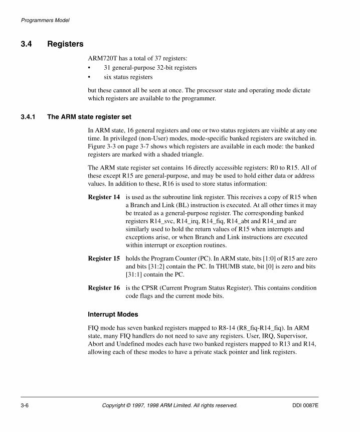
3.4 Registers
ARM720T has a total of 37 registers:
• 31 general-purpose 32-bit registers
• six status registers
but these cannot all be seen at once. The processor state and operating mode dictate which registers are available to the programmer.
3.4.1 The ARM state register set
In ARM state, 16 general registers and one or two status registers are visible at any one time. In privileged (non-User) modes, mode-specific banked registers are switched in. Figure 3-3 on page 3-7 shows which registers are available in each mode: the banked registers are marked with a shaded triangle.
The ARM state register set contains 16 directly accessible registers: R0 to R15. All of these except R15 are general-purpose, and may be used to hold either data or address values. In addition to these, R16 is used to store status information:
Register 14 is used as the subroutine link register. This receives a copy of R15 when a Branch and Link (BL) instruction is executed. At all other times it may be treated as a general-purpose register. The corresponding banked registers R14_svc, R14_irq, R14_fiq, R14_abt and R14_und are similarly used to hold the return values of R15 when interrupts and exceptions arise, or when Branch and Link instructions are executed within interrupt or exception routines.
Register 15 holds the Program Counter (PC). In ARM state, bits [1:0] of R15 are zero and bits [31:2] contain the PC. In THUMB state, bit [0] is zero and bits [31:1] contain the PC.
Register 16 is the CPSR (Current Program Status Register). This contains condition code flags and the current mode bits.
Interrupt Modes
FIQ mode has seven banked registers mapped to R8-14 (R8_fiq-R14_fiq). In ARM state, many FIQ handlers do not need to save any registers. User, IRQ, Supervisor, Abort and Undefined modes each have two banked registers mapped to R13 and R14, allowing each of these modes to have a private stack pointer and link registers.
3-6 Copyright © 1997, 1998 ARM Limited. All rights reserved. DDI 0087E
Programmers Model
Figure 3-3 Register organization in ARM state
DDI 0087E Copyright © 1997, 1998 ARM Limited. All rights reserved. 3-7
Programmers Model
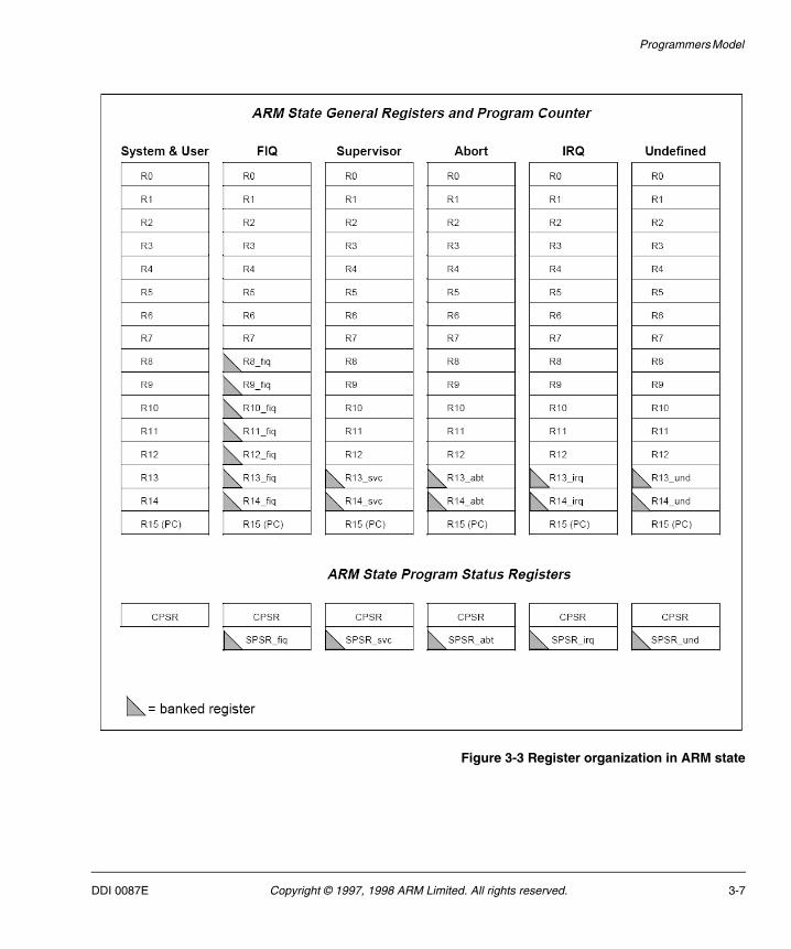
3.4.2 The THUMB state register set
The THUMB state register set is a subset of the ARM state set. The programmer has direct access to:
• eight general registers, (R0 – R7)
• the Program Counter (PC)
• a stack pointer register (SP)
• a link register (LR)
• the CPSR
There are banked Stack Pointers, Link Registers and Saved Process Status Registers (SPSRs) for each privileged mode. This is shown in Figure 3-4.
Figure 3-4 Register organization in THUMB state
3-8 Copyright © 1997, 1998 ARM Limited. All rights reserved. DDI 0087E
Programmers Model
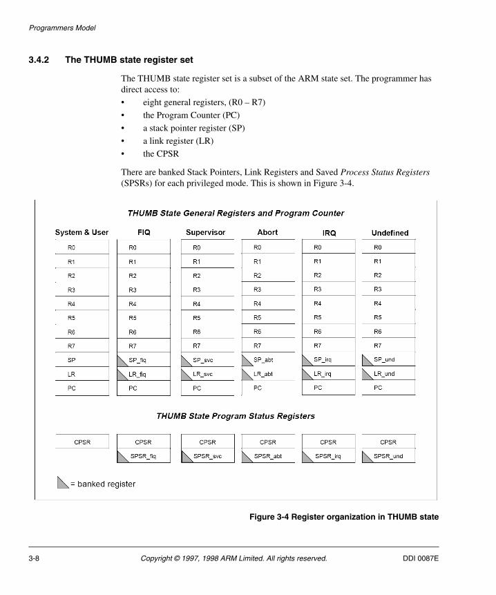
3.4.3 The relationship between ARM and THUMB state registers
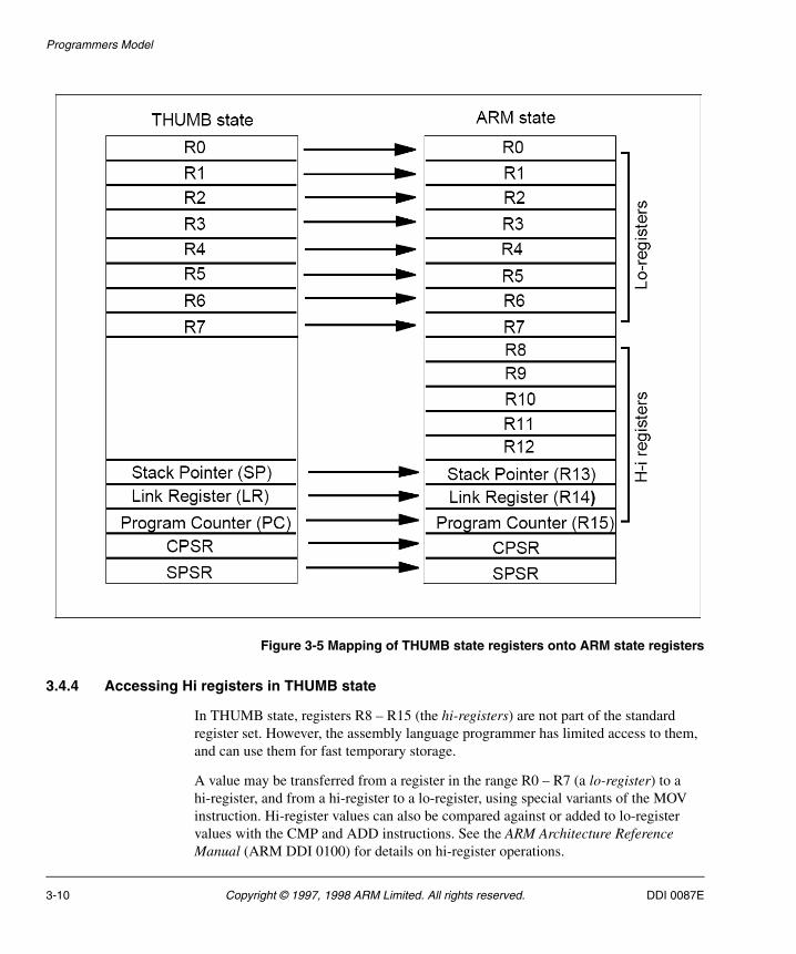
The THUMB state registers relate to the ARM state registers in the following way:
• THUMB state R0 – R7 and ARM state R0 – R7 are identical.
• THUMB state CPSR and SPSRs and ARM state CPSR and SPSRs are identical.
• THUMB state SP maps onto ARM state R13.
• THUMB state LR maps onto ARM state R14.
• The THUMB state Program Counter maps onto the ARM state Program Counter (R15).
This relationship is shown in Figure 3-5 on page 3-10.
DDI 0087E Copyright © 1997, 1998 ARM Limited. All rights reserved. 3-9
Programmers Model
Figure 3-5 Mapping of THUMB state registers onto ARM state registers
3.4.4 Accessing Hi registers in THUMB state
In THUMB state, registers R8 – R15 (the hi-registers) are not part of the standard register set. However, the assembly language programmer has limited access to them, and can use them for fast temporary storage.
A value may be transferred from a register in the range R0 – R7 (a lo-register) to a hi-register, and from a hi-register to a lo-register, using special variants of the MOV instruction. Hi-register values can also be compared against or added to lo-register values with the CMP and ADD instructions. See the ARM Architecture Reference Manual (ARM DDI 0100) for details on hi-register operations.
3-10 Copyright © 1997, 1998 ARM Limited. All rights reserved. DDI 0087E
Programmers Model
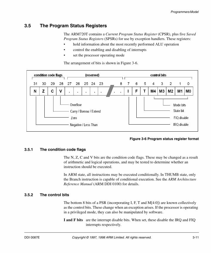
3.5 The Program Status Registers
The ARM720T contains a Current Program Status Register (CPSR), plus five Saved Program Status Registers (SPSRs) for use by exception handlers. These registers:
• hold information about the most recently performed ALU operation
• control the enabling and disabling of interrupts
• set the processor operating mode
The arrangement of bits is shown in Figure 3-6.
Figure 3-6 Program status register format
3.5.1 The condition code flags
The N, Z, C and V bits are the condition code flags. These may be changed as a result of arithmetic and logical operations, and may be tested to determine whether an instruction should be executed.
In ARM state, all instructions may be executed conditionally. In THUMB state, only the Branch instruction is capable of conditional execution. See the ARM Architecture Reference Manual (ARM DDI 0100) for details.
3.5.2 The control bits
The bottom 8 bits of a PSR (incorporating I, F, T and M[4:0]) are known collectively as the control bits. These change when an exception arises. If the processor is operating in a privileged mode, they can also be manipulated by software.
I and F bits are the interrupt disable bits. When set, these disable the IRQ and FIQ interrupts respectively.
DDI 0087E Copyright © 1997, 1998 ARM Limited. All rights reserved. 3-11
Programmers Model
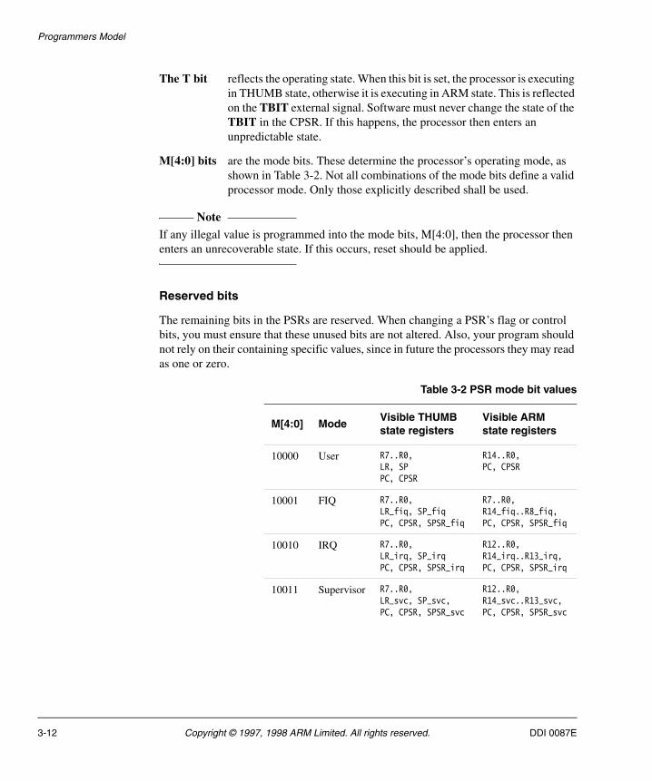
The T bit reflects the operating state. When this bit is set, the processor is executing in THUMB state, otherwise it is executing in ARM state. This is reflected on the TBIT external signal. Software must never change the state of the TBIT in the CPSR. If this happens, the processor then enters an unpredictable state.
M[4:0] bits are the mode bits. These determine the processor’s operating mode, as shown in Table 3-2. Not all combinations of the mode bits define a valid processor mode. Only those explicitly described shall be used.
Note If any illegal value is programmed into the mode bits, M[4:0], then the processor then enters an unrecoverable state. If this occurs, reset should be applied.
Reserved bits
The remaining bits in the PSRs are reserved. When changing a PSR’s flag or control bits, you must ensure that these unused bits are not altered. Also, your program should not rely on their containing specific values, since in future the processors they may read as one or zero.
Table 3-2 PSR mode bit values
M[4:0] ModeVisible THUMB state registers
Visible ARM state registers
10000 User R7..R0,LR, SPPC, CPSR
R14..R0,PC, CPSR
10001 FIQ R7..R0,LR_fiq, SP_fiqPC, CPSR, SPSR_fiq
R7..R0,R14_fiq..R8_fiq,PC, CPSR, SPSR_fiq
10010 IRQ R7..R0,LR_irq, SP_irqPC, CPSR, SPSR_irq
R12..R0,R14_irq..R13_irq,PC, CPSR, SPSR_irq
10011 Supervisor R7..R0,LR_svc, SP_svc,PC, CPSR, SPSR_svc
R12..R0,R14_svc..R13_svc,PC, CPSR, SPSR_svc
3-12 Copyright © 1997, 1998 ARM Limited. All rights reserved. DDI 0087E
Programmers Model
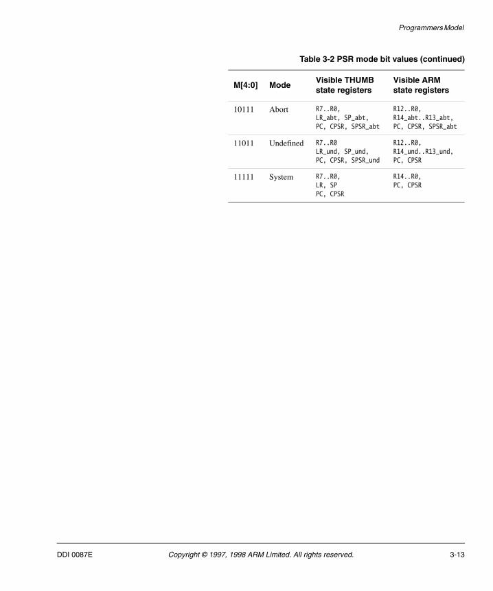
10111 Abort R7..R0,LR_abt, SP_abt,PC, CPSR, SPSR_abt
R12..R0,R14_abt..R13_abt,PC, CPSR, SPSR_abt
11011 Undefined R7..R0LR_und, SP_und,PC, CPSR, SPSR_und
R12..R0,R14_und..R13_und,PC, CPSR
11111 System R7..R0,LR, SPPC, CPSR
R14..R0,PC, CPSR
Table 3-2 PSR mode bit values (continued)
M[4:0] ModeVisible THUMB state registers
Visible ARM state registers
DDI 0087E Copyright © 1997, 1998 ARM Limited. All rights reserved. 3-13
Programmers Model
3.6 Exceptions
Exceptions arise whenever the normal flow of a program has to be halted temporarily, for example to service an interrupt from a peripheral. Before an exception can be handled, the current processor state must be preserved so that the original program can resume when the handler routine has finished.
Several exceptions may arise at the same time. If this happens, they are dealt with in a fixed order - see Exception priorities on page 3-19.
3.6.1 Action on entering an exception
When handling an exception, the ARM720T:
1. Preserves the address of the next instruction in the appropriate Link Register.
• If the exception has been entered from ARM state, the address of the next instruction is copied into the Link Register (that is, current PC + 4 or PC + 8 depending on the exception—see Table 3-3 on page 3-15 for details).
• If the exception has been entered from THUMB state, the value written into the Link Register is the current PC, offset by a value such that the program resumes from the correct place on return from the exception. This means that the exception handler need not determine which state the exception was entered from.
For example, in the case of SWI:
MOVS PC, R14_svc
always returns to the next instruction regardless of whether the SWI was executed in ARM or THUMB state.
2. Copies the CPSR into the appropriate SPSR.
3. Forces the CPSR mode bits to a value which depends on the exception.
4. Forces the PC to fetch the next instruction from the relevant exception vector.
It may also set the interrupt disable flags to prevent otherwise unmanageable nestings of exceptions.
If the processor is in THUMB state when an exception occurs, it automatically switches into ARM state when the PC is loaded with the exception vector address.
3-14 Copyright © 1997, 1998 ARM Limited. All rights reserved. DDI 0087E

Programmers Model
3.6.2 Action on leaving an exception
On completion, the exception handler:
1. Moves the Link Register, minus an offset where appropriate, to the PC. The offset varies depending on the type of exception.
2. Copies the SPSR back to the CPSR.
3. Clears the interrupt disable flags, if they were set on entry.
Note An explicit switch back to THUMB state is never needed, because restoring the CPSR from the SPSR automatically sets the T bit to the value it held immediately prior to the exception.
3.6.3 Exception entry/exit summary
Table 3-3 summarises the PC value preserved in the relevant R14 on exception entry, and the recommended instruction for exiting the exception handler.
Notes
1. Where PC is the address of the BL/SWI/Undefined Instruction fetch that had the prefetch abort.
Table 3-3 Exception entry/exit
Exception Return InstructionPrevious State
NoteARM R14_x THUMB R14_x
BL MOV PC, R14 PC + 4 PC + 2 1
SWI MOVS PC, R14_svc PC + 4 PC + 2 1
UDEF MOVS PC, R14_und PC + 4 PC + 2 1
FIQ SUBS PC, R14_fiq, #4 PC + 4 PC + 4 2
IRQ SUBS PC, R14_irq, #4 PC + 4 PC + 4 2
PABT SUBS PC, R14_abt, #4 PC + 4 PC + 4 1
DABT SUBS PC, R14_abt, #8 PC + 8 PC + 8 3
RESET NA - - 4
DDI 0087E Copyright © 1997, 1998 ARM Limited. All rights reserved. 3-15
Programmers Model
2. Where PC is the address of the instruction that was not executed since the FIQ or IRQ took priority.
3. Where PC is the address of the Load or Store instruction which generated the data abort.
4. The value saved in R14_svc upon reset is unpredictable.
3.6.4 FIQ
The Fast Interrupt Request (FIQ) exception is designed to support a data transfer or channel process, and in ARM state has sufficient private registers to remove the need for register saving (thus minimising the overhead of context switching).
FIQ is externally generated by taking the nFIQ input LOW. nFIQ and nIRQ are considered asynchronous, and a cycle delay for synchronization is incurred before the interrupt can affect the processor flow.
Irrespective of whether the exception was entered from ARM or THUMB state, a FIQ handler should leave the interrupt by executing:
SUBS PC, R14_fiq, #4
FIQ may be disabled by setting the CPSR’s F flag. Note that this is not possible from User mode. If the F flag is clear, ARM720T checks for a LOW level on the output of the FIQ synchronizer at the end of each instruction.
3.6.5 IRQ
The Interrupt Request (IRQ) exception is a normal interrupt caused by a LOW level on the nIRQ input. IRQ has a lower priority than FIQ and is masked out when a FIQ sequence is entered. It may be disabled at any time by setting the I bit in the CPSR, though this can only be done from a privileged (non-User) mode.
Irrespective of whether the exception was entered from ARM or THUMB state, an IRQ handler should return from the interrupt by executing:
SUBS PC, R14_irq, #4
3.6.6 Abort
An abort indicates that the current memory access cannot be completed. It can be signalled either by the Protection unit, or by the external BERROR input. ARM720T checks for the abort exception during memory access cycles.
3-16 Copyright © 1997, 1998 ARM Limited. All rights reserved. DDI 0087E
Programmers Model
There are two types of abort:
Prefetch abort occurs during an instruction prefetch.
Data abort occurs during a data access.
If a prefetch abort occurs, the prefetched instruction is marked as invalid, but the exception is not taken until the instruction reaches the head of the pipeline. If the instruction is not executed—for example because a branch occurs while it is in the pipeline—the abort does not take place.
If a data abort occurs, the action taken depends on the instruction type:
1. Single data transfer instructions (LDR, STR) write back modified base registers: the Abort handler must be aware of this.
2. The swap instruction (SWP) is aborted as though it had not been executed.
3. Block data transfer instructions (LDM, STM) complete. If write-back is set, the base is updated. If the instruction would have overwritten the base with data (that is, it has the base in the transfer list), the overwriting is prevented. All register overwriting is prevented after an abort is indicated, which means in particular that R15 (always the last register to be transferred) is preserved in an aborted LDM instruction.
After fixing the reason for the abort, the handler should execute the following irrespective of the state (ARM or THUMB):
SUBS PC, R14_abt, #4 for a prefetch abort, or
SUBS PC, R14_abt, #8 for a data abort
This restores both the PC and the CPSR, and retries the aborted instruction.
Note There are restrictions on the use of the external abort signal. See External Aborts on page 7-25.
3.6.7 Software interrupt
The software interrupt instruction (SWI) is used for entering Supervisor mode, usually to request a particular supervisor function. A SWI handler should return by executing the following irrespective of the state (ARM or THUMB):
MOV PC, R14_svc
This restores the PC and CPSR, and returns to the instruction following the SWI.
DDI 0087E Copyright © 1997, 1998 ARM Limited. All rights reserved. 3-17
Programmers Model
3.6.8 Undefined instruction
When ARM720T comes across an instruction which it cannot handle, it takes the undefined instruction trap. This mechanism may be used to extend either the THUMB or ARM instruction set by software emulation.
After emulating the failed instruction, the trap handler should execute the following irrespective of the state (ARM or THUMB):
MOVS PC, R14_und
This restores the CPSR and returns to the instruction following the undefined instruction.
3.6.9 Exception vectors
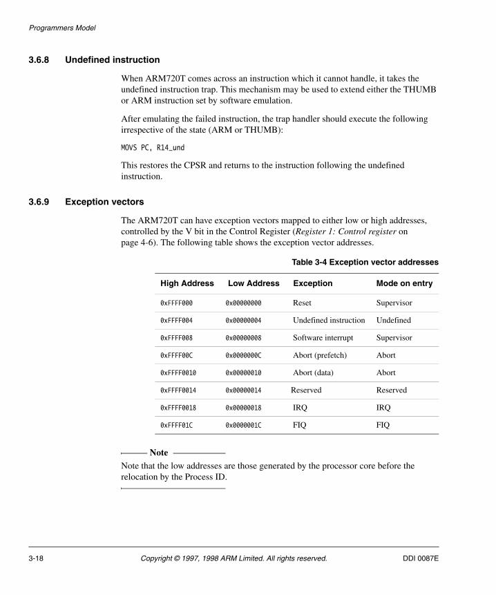
The ARM720T can have exception vectors mapped to either low or high addresses, controlled by the V bit in the Control Register (Register 1: Control register on page 4-6). The following table shows the exception vector addresses.
Note Note that the low addresses are those generated by the processor core before the relocation by the Process ID.
Table 3-4 Exception vector addresses
High Address Low Address Exception Mode on entry
0xFFFF000 0x00000000 Reset Supervisor
0xFFFF004 0x00000004 Undefined instruction Undefined
0xFFFF008 0x00000008 Software interrupt Supervisor
0xFFFF00C 0x0000000C Abort (prefetch) Abort
0xFFFF0010 0x00000010 Abort (data) Abort
0xFFFF0014 0x00000014 Reserved Reserved
0xFFFF0018 0x00000018 IRQ IRQ
0xFFFF01C 0x0000001C FIQ FIQ
3-18 Copyright © 1997, 1998 ARM Limited. All rights reserved. DDI 0087E
Programmers Model
3.6.10 Exception priorities
When multiple exceptions arise at the same time, a fixed priority system determines the order in which they are handled:
1. Reset (Highest priority)
2. Data abort
3. FIQ
4. IRQ
5. Prefetch abort
6. Undefined Instruction, Software interrupt (Lowest priority)
Exception restrictions
Undefined Instruction and Software Interrupt are mutually exclusive, because they each correspond to particular (non-overlapping) decodings of the current instruction.
If a data abort occurs at the same time as a FIQ, and FIQs are enabled (that is, the CPSR’s F flag is clear), ARM720T enters the data abort handler and then immediately proceeds to the FIQ vector. A normal return from FIQ causes the data abort handler to resume execution. Placing data abort at a higher priority than FIQ is necessary to ensure that the transfer error does not escape detection. The time for this exception entry should be added to worst-case FIQ latency calculations.
DDI 0087E Copyright © 1997, 1998 ARM Limited. All rights reserved. 3-19

Programmers Model
3.7 Reset
When the BnRES signal goes LOW, ARM720T:
1. Abandons the executing instruction.
2. Flushes the Cache and Translation Lookaside Buffer.
3. Disables the Write Buffer, Cache and Memory Management Unit.
4. Resets the Process Identifier.
5. Continues to fetch instructions from incrementing word addresses.
When BnRES goes HIGH again, ARM720T:
1. Overwrites R14_svc and SPSR_svc by copying the current values of the PC and CPSR into them. The value of the saved PC and SPSR is not defined.
2. Forces M[4:0] to 10011 (Supervisor mode), sets the I and F bits in the CPSR, and clears the CPSR’s T bit.
3. Forces the PC to fetch the next instruction from the low reset exception vector.
4. Resumes execution in ARM state.
3-20 Copyright © 1997, 1998 ARM Limited. All rights reserved. DDI 0087E
Programmers Model
3.8 Relocation of Low Virtual Addresses by Process Identifier
The virtual address produced by the processor core going to the IDC and MMU may be relocated if it lies in the bottom 32MB of the virtual address (that is, virtual address bits [31:25] = 0000000) by the substitution of the seven bits [31:25] of the ProcessID register in the CP15 Coprocessor.
The two instructions fetched immediately following an instruction to change the Process Identifier are fetched with a relocation to the previous Process Identifier, if the addresses of the instructions being fetched lie within the range of addresses to be relocated. In this behaviour, a change to the Process Identifier exhibits similar behaviour to a delayed branch.
On reset, the Process Identifier register bits [31:25] are set to 0000000, thus disabling all relocation. For this reason, the low address reset exception vector is effectively never relocated by this mechanism.
Relocation of the virtual address only occurs if the WinCE Enhancements pin is at a logic “1”; that is, the WinCE Enhancements are enabled.
Note All addresses produced by the processor core undergo this translation if they lie in the appropriate address range; this includes the exception vectors if they are configured to lie in the bottom of the virtual memory map (this configuration is determined by the Vbit in the CP15 Control Register).
DDI 0087E Copyright © 1997, 1998 ARM Limited. All rights reserved. 3-21
Programmers Model
3.9 Implementation-defined Behaviour of Instructions
The ARM Architectural Reference Manual defines the instruction set of the ARM720T. The following list defines the behaviour of the ARM720T instructions for those features which are denoted as being implementation defined in that manual.
Indexed Addressing on a Data abort
For the following instructions:
• LDC
• LDM
• LDR
• LDRB
• LDRBT
• LDRH
• LDRSB
• LDRSH
• LDRT
in the event of a data abort with pre-indexed or post-indexed addressing, the value left in Rn is defined to be the updated base register value.
For the following instructions:
• STC
• STM
• STR
• STRB
• STRBT
• STRH
• STRT
in the event of a data abort with pre-indexed or post-indexed addressing, the value left in Rn is defined to be the updated base register value.
Early Termination
On the ARM720T, early termination is defined as:
MLA, MUL signed early termination.
SMULL, SMLAL signed early termination.
UMULL, UMLAL unsigned early termination.
3-22 Copyright © 1997, 1998 ARM Limited. All rights reserved. DDI 0087E

Chapter 4 Configuration
This chapter describes the configuration of the ARM720T.
• Overview on page 4-2
• Internal Coprocessor Instructions on page 4-4
• Registers on page 4-5.
DDI 0087E Copyright © 1997, 1998 ARM Limited. All rights reserved. 4-1
Configuration
4.1 Overview
The operation and configuration of ARM720T is controlled:
• directly via coprocessor instructions
• indirectly via the Memory Management Page tables
The coprocessor instructions manipulate a number of on-chip registers which control the configuration of the following:
• Cache
• write buffer
• MMU
• a number of other configuration options
4.1.1 Compatibility
To ensure backwards compatibility of future CPUs:
1. All reserved or unused bits in registers and coprocessor instructions should be programmed to “0”.
2. Invalid registers must not be read/written.
3. The following bits must be programmed to “0”:
Register 1 bits[31:14] and bits [12:10]
Register 2 bits[13:0]
Register 5 bits[31:9]
Register 7 bits[31:0]
Register 13 bits[24:0]
Note The gray areas in the register and translation diagrams are reserved and should be programmed 0 for future compatibility.
4.1.2 Notation
Throughout this section, the following terms and abbreviations are used:
unpredictable (unp) If specified for reads: the data returned when reading from this location is unpredictable—it could have any value.
4-2 Copyright © 1997, 1998 ARM Limited. All rights reserved. DDI 0087E
Configuration
If specified for writes: writing to this location causes unpredictable behaviour or an unpredictable change in device configuration.
should be zero (sbz) When writing to this location, all bits of this field should be 0.
DDI 0087E Copyright © 1997, 1998 ARM Limited. All rights reserved. 4-3
Configuration
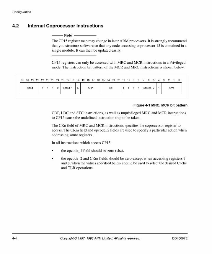
4.2 Internal Coprocessor Instructions
Note The CP15 register map may change in later ARM processors. It is strongly recommend that you structure software so that any code accessing coprocessor 15 is contained in a single module. It can then be updated easily.
CP15 registers can only be accessed with MRC and MCR instructions in a Privileged mode. The instruction bit pattern of the MCR and MRC instructions is shown below.
Figure 4-1 MRC, MCR bit pattern
CDP, LDC and STC instructions, as well as unprivileged MRC and MCR instructions to CP15 cause the undefined instruction trap to be taken.
The CRn field of MRC and MCR instructions specifies the coprocessor register to access. The CRm field and opcode_2 fields are used to specify a particular action when addressing some registers.
In all instructions which access CP15:
• the opcode_1 field should be zero (sbz).
• the opcode_2 and CRm fields should be zero except when accessing registers 7 and 8, when the values specified below should be used to select the desired Cache and TLB operations.
4-4 Copyright © 1997, 1998 ARM Limited. All rights reserved. DDI 0087E
Configuration
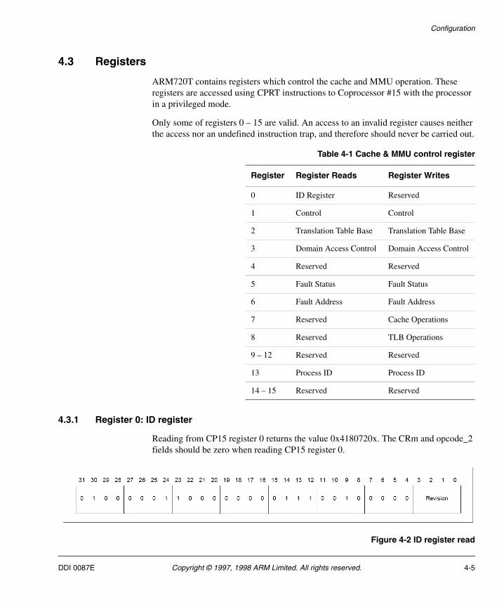
4.3 Registers
ARM720T contains registers which control the cache and MMU operation. These registers are accessed using CPRT instructions to Coprocessor #15 with the processor in a privileged mode.
Only some of registers 0 – 15 are valid. An access to an invalid register causes neither the access nor an undefined instruction trap, and therefore should never be carried out.
4.3.1 Register 0: ID register
Reading from CP15 register 0 returns the value 0x4180720x. The CRm and opcode_2 fields should be zero when reading CP15 register 0.
Figure 4-2 ID register read
Table 4-1 Cache & MMU control register
Register Register Reads Register Writes
0 ID Register Reserved
1 Control Control
2 Translation Table Base Translation Table Base
3 Domain Access Control Domain Access Control
4 Reserved Reserved
5 Fault Status Fault Status
6 Fault Address Fault Address
7 Reserved Cache Operations
8 Reserved TLB Operations
9 – 12 Reserved Reserved
13 Process ID Process ID
14 – 15 Reserved Reserved
DDI 0087E Copyright © 1997, 1998 ARM Limited. All rights reserved. 4-5

Configuration
Writing to CP15 register 0 is unpredictable.
Figure 4-3 ID register write
4.3.2 Register 1: Control register
Reading from CP15 register 1 reads the control bits. The CRm and opcode_2 fields should be zero when reading CP15 register 1.
Figure 4-4 Register 1 read
Writing to CP15 register 1 sets the control bits. The CRm and opcode_2 fields should be zero when writing CP15 register 1.
Figure 4-5 Register 1 write
All defined control bits are set to zero on reset. The control bits have the following functions:
M Bit 0 MMU Enable/Disable
0 = Memory Management Unit (MMU) disabled
1 = Memory Management Unit (MMU) enabled
A Bit 1 Alignment Fault Enable/Disable
0 = Address Alignment Fault Checking disabled
4-6 Copyright © 1997, 1998 ARM Limited. All rights reserved. DDI 0087E
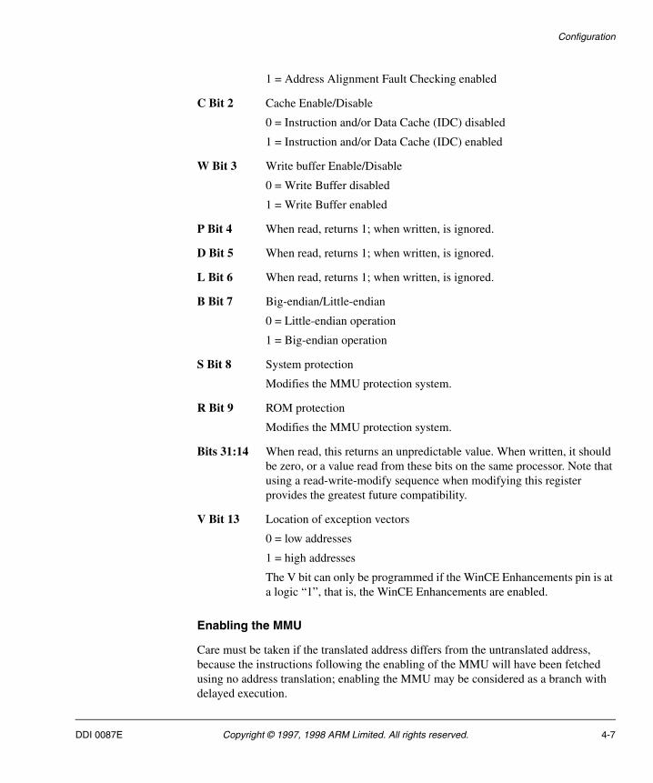
Configuration
1 = Address Alignment Fault Checking enabled
C Bit 2 Cache Enable/Disable
0 = Instruction and/or Data Cache (IDC) disabled
1 = Instruction and/or Data Cache (IDC) enabled
W Bit 3 Write buffer Enable/Disable
0 = Write Buffer disabled
1 = Write Buffer enabled
P Bit 4 When read, returns 1; when written, is ignored.
D Bit 5 When read, returns 1; when written, is ignored.
L Bit 6 When read, returns 1; when written, is ignored.
B Bit 7 Big-endian/Little-endian
0 = Little-endian operation
1 = Big-endian operation
S Bit 8 System protection
Modifies the MMU protection system.
R Bit 9 ROM protection
Modifies the MMU protection system.
Bits 31:14 When read, this returns an unpredictable value. When written, it should be zero, or a value read from these bits on the same processor. Note that using a read-write-modify sequence when modifying this register provides the greatest future compatibility.
V Bit 13 Location of exception vectors
0 = low addresses
1 = high addresses
The V bit can only be programmed if the WinCE Enhancements pin is at a logic “1”, that is, the WinCE Enhancements are enabled.
Enabling the MMU
Care must be taken if the translated address differs from the untranslated address, because the instructions following the enabling of the MMU will have been fetched using no address translation; enabling the MMU may be considered as a branch with delayed execution.
DDI 0087E Copyright © 1997, 1998 ARM Limited. All rights reserved. 4-7

Configuration
A similar situation occurs when the MMU is disabled. The correct code sequence for enabling and disabling the MMU is given in Interaction of the MMU, IDC and Write Buffer on page 7-26.
If the cache and write buffer are enabled when the MMU is not enabled, the results are unpredictable.
4.3.3 Register 2: Translation table base register
Reading from CP15 register 2 returns the pointer to the currently active first-level translation table in bits [31:14] and an unpredictable value in bits [13:0]. The CRm and opcode_2 fields should be zero when reading CP15 register 2.
Writing to CP15 register 2 updates the pointer to the currently active first-level translation table from the value in bits [31:14] of the written value. Bits [13:0] should be zero. The CRm and opcode_2 fields should be zero when writing CP15 register 2.
Figure 4-6 Register 2
4.3.4 Register 3: Domain access control register
Reading from CP15 register 3 returns the value of the Domain Access Control Register.
Writing to CP15 register 3 writes the value of Domain Access Control Register.
The Domain Access Control Register consists of 16 2-bit fields, each of which defines the access permissions for one of the 16 Domains (D15-D0).
The CRm and opcode_2 fields should be zero when reading or writing CP15 register 3.
Figure 4-7 Register 3
4-8 Copyright © 1997, 1998 ARM Limited. All rights reserved. DDI 0087E
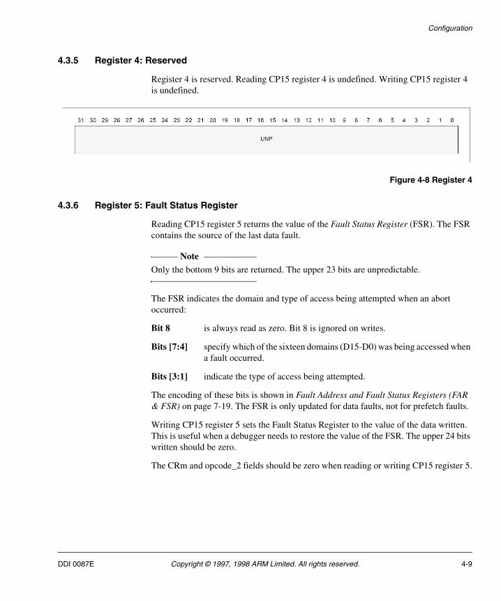
Configuration
4.3.5 Register 4: Reserved
Register 4 is reserved. Reading CP15 register 4 is undefined. Writing CP15 register 4 is undefined.
Figure 4-8 Register 4
4.3.6 Register 5: Fault Status Register
Reading CP15 register 5 returns the value of the Fault Status Register (FSR). The FSR contains the source of the last data fault.
Note Only the bottom 9 bits are returned. The upper 23 bits are unpredictable.
The FSR indicates the domain and type of access being attempted when an abort occurred:
Bit 8 is always read as zero. Bit 8 is ignored on writes.
Bits [7:4] specify which of the sixteen domains (D15-D0) was being accessed when a fault occurred.
Bits [3:1] indicate the type of access being attempted.
The encoding of these bits is shown in Fault Address and Fault Status Registers (FAR & FSR) on page 7-19. The FSR is only updated for data faults, not for prefetch faults.
Writing CP15 register 5 sets the Fault Status Register to the value of the data written. This is useful when a debugger needs to restore the value of the FSR. The upper 24 bits written should be zero.
The CRm and opcode_2 fields should be zero when reading or writing CP15 register 5.
DDI 0087E Copyright © 1997, 1998 ARM Limited. All rights reserved. 4-9
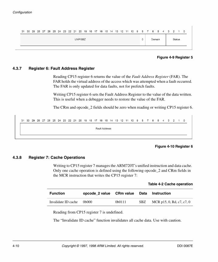
Configuration
Figure 4-9 Register 5
4.3.7 Register 6: Fault Address Register
Reading CP15 register 6 returns the value of the Fault Address Register (FAR). The FAR holds the virtual address of the access which was attempted when a fault occurred. The FAR is only updated for data faults, not for prefetch faults.
Writing CP15 register 6 sets the Fault Address Register to the value of the data written. This is useful when a debugger needs to restore the value of the FAR.
The CRm and opcode_2 fields should be zero when reading or writing CP15 register 6.
Figure 4-10 Register 6
4.3.8 Register 7: Cache Operations
Writing to CP15 register 7 manages the ARM720T’s unified instruction and data cache. Only one cache operation is defined using the following opcode_2 and CRm fields in the MCR instruction that writes the CP15 register 7:
Reading from CP15 register 7 is undefined.
The “Invalidate ID cache” function invalidates all cache data. Use with caution.
Table 4-2 Cache operation
Function opcode_2 value CRm value Data Instruction
Invalidate ID cache 0b000 0b0111 SBZ MCR p15, 0, Rd, c7, c7, 0
4-10 Copyright © 1997, 1998 ARM Limited. All rights reserved. DDI 0087E

Configuration
4.3.9 Register 8: TLB Operations
Writing to CP15 register 8 is used to control the Translation Lookaside Buffer (TLB). The ARM720T implements a unified instruction and data TLB.
Two TLB operations are defined, and the function to be performed selected by the opcode_2 and CRm fields in the MCR instruction used to write CP15 register 8.
Reading from CP15 register 8 is undefined.
The “Invalidate TLB” function invalidates all of the unlocked entries in the TLB.
The “Invalidate TLB single entry” function invalidates any TLB entry corresponding to the Virtual Address given in Rd.
4.3.10 Registers 9 – 12: Reserved
Accessing any of these registers is undefined. Writing to any of these registers is undefined.
4.3.11 Register 13: Process Identifier
Reading from CP15 register returns the value of the Process Identifier.
Figure 4-11 Register 13
The Process Identifier can only be accessed if the WinCe pin is at a logic “1”;that is, the WinCE Enhancements are enabled.
Note Only bits [31:25] are returned. The remaining 25 bits are unpredictable.
Table 4-3 TLB operations
Function opcode_2 value CRm value Data Instruction
Invalidate TLB 0b000 0b0111 SBZ MCR p15, 0, Rd, c8, c7, 0
Invalidate TLB single entry 0b001 0b0111 Virtual Address MCR p15, 0, Rd, c8, c7, 1
DDI 0087E Copyright © 1997, 1998 ARM Limited. All rights reserved. 4-11
Configuration
Writing to CP15 register updates the process identifier from the value in bits [31:25]. Bits [24:0] should be zero. The Process Identifier is set to 0000000 on Reset. The CRm and opcode_2 should be zero when reading or writing CP15 register 13.
Changing Process Identifier
Care must be taken when changing Process Identifier as the following instructions will have been fetched with the Process Identifier. In this respect, changing the Process Identifier has similarities with a branch with delayed execution. See Relocation of Low Virtual Addresses by Process Identifier on page 3-21.
4.3.12 Registers 14-15: Reserved
Accessing any of these registers is undefined. Writing to any of these registers is undefined.
4-12 Copyright © 1997, 1998 ARM Limited. All rights reserved. DDI 0087E
Chapter 5 Instruction and Data Cache (IDC)
This chapter describes the instruction and data cache.
1. Overview of the Instruction and Data Cache on page 5-2
2. IDC Validity on page 5-4
3. IDC Enable/Disable and Reset on page 5-5.
DDI 0087E Copyright © 1997, 1998 ARM Limited. All rights reserved. 5-1
Instruction and Data Cache (IDC)
5.1 Overview of the Instruction and Data Cache
5.1.1 IDC operation
ARM720T contains an 8KB mixed instruction and data cache (IDC).
The C bit in the ARM720T Control Register and the Cacheablebitin the MMU page tables only affect loading data into the Cache. The Cache is always searched regardless of these two bits. If the data is found then it is used, so when the cache is disabled, it should also be flushed.
The IDC has 512 lines of 16 bytes (four words), arranged as a 4-way set-associative cache, and uses the virtual addresses generated by the processor core after relocation by the Process Identifier as appropriate. The IDC is always reloaded a line at a time (4 words). It may be enabled or disabled via the ARM720T Control Register and is disabled on BnRES.
The operation of the cache is further controlled by the Cacheable (C bit) stored in the Memory Management Page Table—see Chapter 7 Memory Management Unit (MMU). For this reason, the MMU must be enabled in order to use the IDC. However, the two functions may be enabled simultaneously, with a single write to the Control Register.
5.1.2 Cacheable bit
The Cacheable bit determines whether data being read may be placed in the IDC and used for subsequent read operations. Typically, main memory is marked as cacheable to improve system performance, and I/O space as non-cacheable to stop the data being stored in ARM720T's cache.
For example, if the processor is polling a hardware flag in I/O space, it is important that the processor is forced to read data from the external peripheral, and not a copy of the initial data held in the cache. The Cacheable bit can be configured for both pages and sections.
Cacheable reads (C = 1)
A linefetch of four words is performed when a cache miss occurs in a cacheable area of memory, and it is randomly placed in a cache bank.
Uncacheable reads (C = 0)
An external memory access is performed and the cache is not written.
5-2 Copyright © 1997, 1998 ARM Limited. All rights reserved. DDI 0087E
Instruction and Data Cache (IDC)
5.1.3 DC operation
The C bit in the ARM720T Control Register and the Cacheable bit in the MMU page tables only affect loading data into the Cache. The Cache is always searched regardless of these two bits. If the data is found it is used, so when the cache is disabled, it should also be flushed.
5.1.4 Read-lock-write
The IDC treats the Read-Locked-Write instruction as a special case.
The read phase always forces a read of external memory, regardless of whether the data is contained in the cache.
The write phase is treated as a normal write operation. If the data is already in the cache, the cache is updated.
Externally, the two phases are flagged as indivisible by asserting the BLOK signal.
DDI 0087E Copyright © 1997, 1998 ARM Limited. All rights reserved. 5-3
Instruction and Data Cache (IDC)
5.2 IDC Validity
The IDC operates with virtual addresses, so you must ensure that its contents remain consistent with the virtual to physical mappings performed by the MMU. If the memory mappings are changed, the IDC validity must be ensured.
5.2.1 Software IDC flush
The entire IDC may be marked as invalid by writing to the Cache Operations Register (R7). The cache is flushed immediately the register is written, but note that the two instruction fetches following may come from the cache before the register is written.
5.2.2 Doubly-mapped space
As the cache works with virtual addresses, it is assumed that every virtual address maps to a different physical address. If the same physical location is accessed by more than one virtual address, the cache cannot maintain consistency. Each virtual address has a separate entry in the cache, and only one entry can be updated on a processor write operation.
To avoid any cache inconsistencies, both doubly-mapped virtual addresses should be marked as uncacheable.
5-4 Copyright © 1997, 1998 ARM Limited. All rights reserved. DDI 0087E
Instruction and Data Cache (IDC)
5.3 IDC Enable/Disable and Reset
The IDC is automatically disabled and flushed on BnRES. Once enabled, cacheable read accesses causes lines to be placed in the cache.
To enable the IDC
1. Make sure that the MMU is enabled first by setting bit 0 in the Control register.
2. Enable the IDC by setting bit 2 in the Control register. The MMU and IDC may be enabled simultaneously with a single write to the control register.
To disable the IDC
1. Clear bit 2 in the Control register.
2. Perform a flush by writing to the Cache Operations register.
DDI 0087E Copyright © 1997, 1998 ARM Limited. All rights reserved. 5-5
Instruction and Data Cache (IDC)
5-6 Copyright © 1997, 1998 ARM Limited. All rights reserved. DDI 0087E

Chapter 6 Write Buffer
This chapter describes the Write Buffer.
• Overview on page 6-2
• Write Buffer Operation on page 6-3.
DDI 0087E Copyright © 1997, 1998 ARM Limited. All rights reserved. 6-1
Write Buffer
6.1 Overview
The ARM720T write buffer is provided to improve system performance. It can buffer up to eight words of data, and four independent addresses. It may be enabled or disabled via the W bit (bit 3) in the ARM720T Control Register. The buffer is disabled and flushed on reset.
The operation of the write buffer is further controlled by the Bufferable (B) bit, which is stored in the Memory Management Page Tables. For this reason, the MMU must be enabled so you can use the write buffer. The two functions may however be enabled simultaneously, with a single write to the Control Register.
For a write to use the write buffer, both the W bit in the Control Register and the B bit in the corresponding page table must be set.
Note It is not possible to abort buffered writes externally; the BERROR pin is ignored. Areas of memory which may generate aborts should be marked as unbufferable in the MMU page tables.
6.1.1 Bufferable bit
This bit controls whether a write operation may or may not use the write buffer. Typically, main memory is bufferable and I/O space unbufferable. The Bufferable bit can be configured for both pages and sections.
6-2 Copyright © 1997, 1998 ARM Limited. All rights reserved. DDI 0087E
Write Buffer
6.2 Write Buffer Operation
When the CPU performs a write operation, the translation entry for that address is inspected and the state of the B bit determines the subsequent action. If the write buffer is disabled via the ARM720T Control Register, buffered writes are treated in the same way as unbuffered writes.
To enable the write buffer
1. Ensure the MMU is enabled by setting bit 0 in the Control Register.
2. Enable the write buffer by setting bit 3 in the Control Register. The MMU and write buffer may be enabled simultaneously with a single write to the Control Register.
To disable the write buffer
1. Clear bit 3 in the Control Register.
Note Any writes already in the write buffer complete normally.
6.2.1 Bufferable write
If the write buffer is enabled and the processor performs a write to a bufferable area, the data is placed in the write buffer at FCLK speeds (BCLK if running with fastbus extension) and the CPU continues execution. The write buffer then performs the external write in parallel.
If the write buffer is full (either because there are already eight words of data in the buffer, or because there is no slot for the new address), the processor is stalled until there is sufficient space in the buffer.
6.2.2 Unbufferable writes
If the write buffer is disabled or the CPU performs a write to an unbufferable area, the processor is stalled until the write buffer empties and the write completes externally. This may require synchronisation and several external clock cycles.
6.2.3 Read-lock-write
The write phase of a read-lock-write sequence is treated as an unbuffered write, even if it is marked as buffered.
DDI 0087E Copyright © 1997, 1998 ARM Limited. All rights reserved. 6-3
Write Buffer
Note A single write requires one address slot and one data slot in the write buffer; a sequential write of n words requires one address slot and n data slots. The total of eight data slots in the buffer may be used as required. For example, there could be three non-sequential writes and one sequential write of five words in the buffer, and the processor could continue as normal: a fifth write or a sixth word in the fourth write would stall the processor until the first write had completed.
6-4 Copyright © 1997, 1998 ARM Limited. All rights reserved. DDI 0087E
Chapter 7 Memory Management Unit (MMU)
This chapter describes the Memory Management Unit.
• Overview on page 7-2
• MMU Program Accessible Registers on page 7-4
• Address Translation Process on page 7-5
• Level 1 Descriptor on page 7-7
• Page Table Descriptor on page 7-8
• Section Descriptor on page 7-9
• Translating Section References on page 7-11
• Level 2 Descriptor on page 7-12
• Translating Small Page References on page 7-14
• Translating Large Page References on page 7-16
• MMU Faults and CPU Aborts on page 7-18
• Fault Address and Fault Status Registers (FAR & FSR) on page 7-19
• Domain Access Control on page 7-21
• Fault Checking Sequence on page 7-22
• External Aborts on page 7-25
• Interaction of the MMU, IDC and Write Buffer on page 7-26.
DDI 0087E Copyright © 1997, 1998 ARM Limited. All rights reserved. 7-1

Memory Management Unit (MMU)
7.1 Overview
The Memory Management MMU performs two primary functions. It:
• translates virtual addresses into physical addresses
• controls memory access permissions
The MMU hardware required to perform these functions consists of:
• a Translation Look-aside Buffer (TLB)
• access control logic
• translation-table-walking logic
When the MMU is turned off (as happens on reset), the virtual address is output directly onto the physical address bus.
Note The MMU works with virtual addresses after any relocation by the Process Identifier.
7.1.1 Memory accesses
The MMU supports memory accesses based on Sections or Pages:
Sections are 1MB blocks of memory.
Pages Two different page sizes are supported:
Small Pages consist of 4KB blocks of memory. Additional access control mechanisms are extended to 1KB Sub-Pages.
Large Pages consist of 64KB blocks of memory. Large Pages are supported to allow mapping of a large region of memory while using only a single entry in the TLB).
Additional access control mechanisms are extended to 16KB Sub-Pages.
7.1.2 Domains
The MMU also supports the concept of domains, which are areas of memory that can be defined to possess individual access rights. The Domain Access Control Register is used to specify access rights for up to 16 separate domains.
7-2 Copyright © 1997, 1998 ARM Limited. All rights reserved. DDI 0087E

Memory Management Unit (MMU)
7.1.3 TLB
The TLB caches 64 translated entries. During most memory accesses, the TLB provides the translation information to the access control logic.
• If the TLB contains a translated entry for the virtual address, the access control logic determines whether access is permitted.
• If access is permitted, the MMU outputs the appropriate physical address corresponding to the virtual address.
• If access is not permitted, the MMU signals the CPU to abort.
If the TLB misses (it does not contain a translated entry for the virtual address), the translation-table-walking hardware is invoked to retrieve the translation information from a translation table in physical memory. Once retrieved, the translation information is placed into the TLB, possibly overwriting an existing value. The entry to be overwritten is chosen by cycling sequentially through the TLB locations.
7.1.4 Effect of reset
For information on the effect of reset, see Reset on page 3-20.
DDI 0087E Copyright © 1997, 1998 ARM Limited. All rights reserved. 7-3
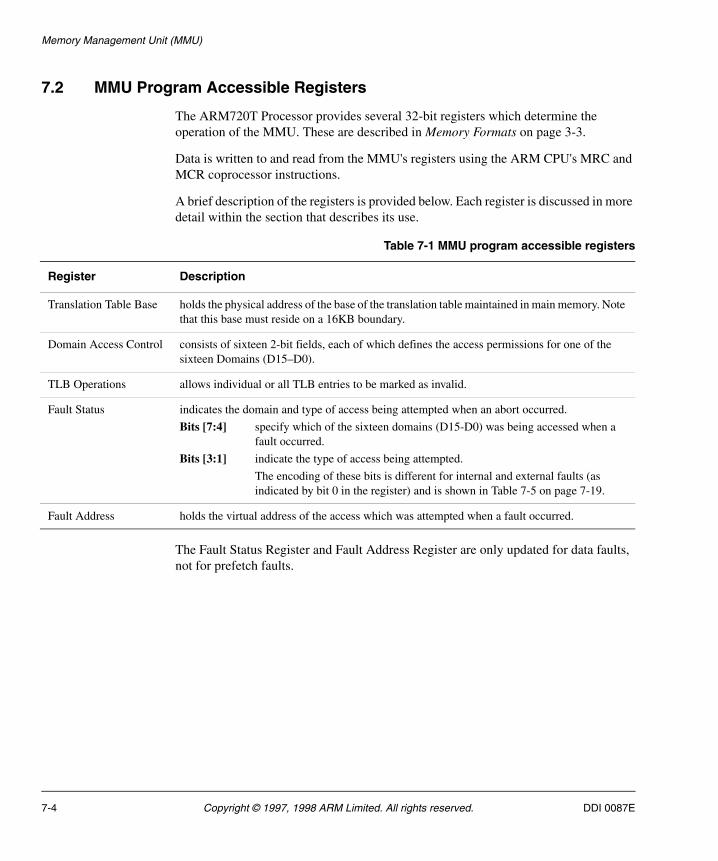
Memory Management Unit (MMU)
7.2 MMU Program Accessible Registers
The ARM720T Processor provides several 32-bit registers which determine the operation of the MMU. These are described in Memory Formats on page 3-3.
Data is written to and read from the MMU's registers using the ARM CPU's MRC and MCR coprocessor instructions.
A brief description of the registers is provided below. Each register is discussed in more detail within the section that describes its use.
The Fault Status Register and Fault Address Register are only updated for data faults, not for prefetch faults.
Table 7-1 MMU program accessible registers
Register Description
Translation Table Base holds the physical address of the base of the translation table maintained in main memory. Note that this base must reside on a 16KB boundary.
Domain Access Control consists of sixteen 2-bit fields, each of which defines the access permissions for one of the sixteen Domains (D15–D0).
TLB Operations allows individual or all TLB entries to be marked as invalid.
Fault Status indicates the domain and type of access being attempted when an abort occurred.
Bits [7:4] specify which of the sixteen domains (D15-D0) was being accessed when a fault occurred.
Bits [3:1] indicate the type of access being attempted.
The encoding of these bits is different for internal and external faults (as indicated by bit 0 in the register) and is shown in Table 7-5 on page 7-19.
Fault Address holds the virtual address of the access which was attempted when a fault occurred.
7-4 Copyright © 1997, 1998 ARM Limited. All rights reserved. DDI 0087E
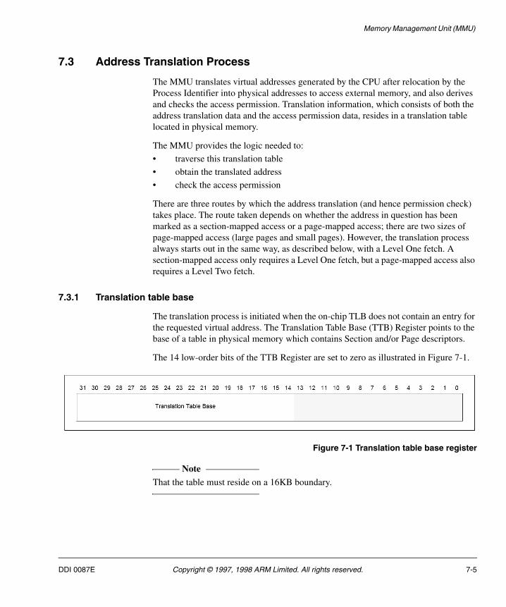
Memory Management Unit (MMU)
7.3 Address Translation Process
The MMU translates virtual addresses generated by the CPU after relocation by the Process Identifier into physical addresses to access external memory, and also derives and checks the access permission. Translation information, which consists of both the address translation data and the access permission data, resides in a translation table located in physical memory.
The MMU provides the logic needed to:
• traverse this translation table
• obtain the translated address
• check the access permission
There are three routes by which the address translation (and hence permission check) takes place. The route taken depends on whether the address in question has been marked as a section-mapped access or a page-mapped access; there are two sizes of page-mapped access (large pages and small pages). However, the translation process always starts out in the same way, as described below, with a Level One fetch. A section-mapped access only requires a Level One fetch, but a page-mapped access also requires a Level Two fetch.
7.3.1 Translation table base
The translation process is initiated when the on-chip TLB does not contain an entry for the requested virtual address. The Translation Table Base (TTB) Register points to the base of a table in physical memory which contains Section and/or Page descriptors.
The 14 low-order bits of the TTB Register are set to zero as illustrated in Figure 7-1.
Figure 7-1 Translation table base register
Note That the table must reside on a 16KB boundary.
DDI 0087E Copyright © 1997, 1998 ARM Limited. All rights reserved. 7-5
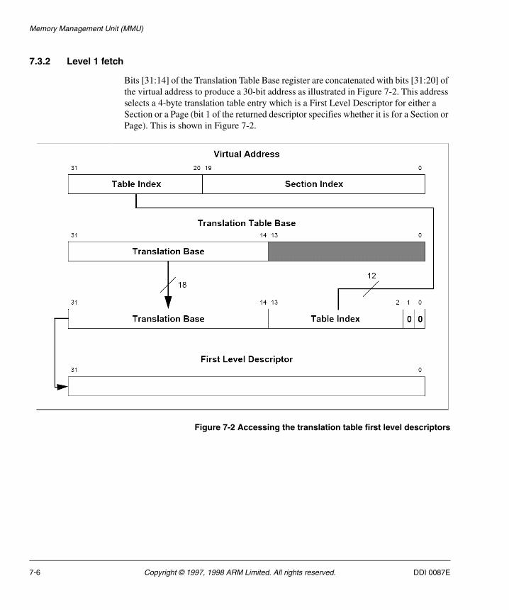
Memory Management Unit (MMU)
7.3.2 Level 1 fetch
Bits [31:14] of the Translation Table Base register are concatenated with bits [31:20] of the virtual address to produce a 30-bit address as illustrated in Figure 7-2. This address selects a 4-byte translation table entry which is a First Level Descriptor for either a Section or a Page (bit 1 of the returned descriptor specifies whether it is for a Section or Page). This is shown in Figure 7-2.
Figure 7-2 Accessing the translation table first level descriptors
7-6 Copyright © 1997, 1998 ARM Limited. All rights reserved. DDI 0087E
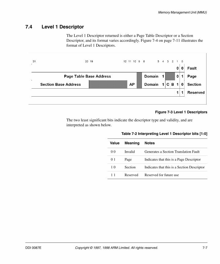
Memory Management Unit (MMU)
7.4 Level 1 Descriptor
The Level 1 Descriptor returned is either a Page Table Descriptor or a Section Descriptor, and its format varies accordingly. Figure 7-4 on page 7-11 illustrates the format of Level 1 Descriptors.
Figure 7-3 Level 1 Descriptors
The two least significant bits indicate the descriptor type and validity, and are interpreted as shown below.
Table 7-2 Interpreting Level 1 Descriptor bits [1:0]
Value Meaning Notes
0 0 Invalid Generates a Section Translation Fault
0 1 Page Indicates that this is a Page Descriptor
1 0 Section Indicates that this is a Section Descriptor
1 1 Reserved Reserved for future use
DDI 0087E Copyright © 1997, 1998 ARM Limited. All rights reserved. 7-7
Memory Management Unit (MMU)
7.5 Page Table Descriptor
Bits [3:2] are always written as 0.
Bit [4] should be written to 1 for backward compatibility.
Bits [8:5] specify one of the 16 possible domains (held in the Domain Access Control Register) that contain the primary access controls.
Bits [31:10] form the base for referencing the Page Table Entry. (The page table index for the entry is derived from the virtual address as illustrated in Figure 7-6 on page 7-15).
If a Page Table Descriptor is returned from the Level One fetch, a Level Two fetch is initiated as described in the following section.
7-8 Copyright © 1997, 1998 ARM Limited. All rights reserved. DDI 0087E

Memory Management Unit (MMU)
7.6 Section Descriptor
C (Cacheable): indicates that data at this address is placed in the cache (if the cache is enabled).
B (Bufferable): indicates that data at this address is written through the write buffer (if the write buffer is enabled).
Note The meaning of the C and B bits may change in later ARM processors. It is strongly recommend that you structure software so that code which manipulates the MMU page tables is contained in a single module. It can then be updated easily when you port it to a different ARM processor.
Bits [3:2] (C, B) control the cache- and write-buffer-related functions.
Bit [4] should be written to 1 for backward compatibility.
Bits [8:5] specify one of the 16 possible domains (held in the Domain Access Control Register) that contain the primary access controls.
Bits [11:10] (AP) specify the access permissions for this section and are interpreted as shown in Table 7-3. Their interpretation depends on the setting of the S and R bits (control register bits 8 and 9). The Domain Access Control specifies the primary access control; the AP bits only have an effect in client mode. Refer to Domain Access Control on page 7-21.
Bits [19:12] are always written as 0.
Bits [31:20] form the corresponding bits of the physical address for the 1MB section.
Table 7-3 Interpreting access permission (AP) bits
AP S RSupervisor Permission
User Permission
Notes
00 0 0 No Access No Access Any access generates a permission fault
00 1 0 Read Only No Access Supervisor Read Only permitted
00 0 1 Read Only Read Only Any write generates a permission fault
00 1 1 Reserved Reserved Reserved
01 x x Read/Write No Access Access allowed only in Supervisor mode
DDI 0087E Copyright © 1997, 1998 ARM Limited. All rights reserved. 7-9
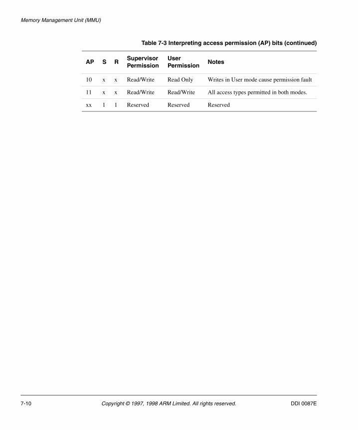
Memory Management Unit (MMU)
10 x x Read/Write Read Only Writes in User mode cause permission fault
11 x x Read/Write Read/Write All access types permitted in both modes.
xx 1 1 Reserved Reserved Reserved
Table 7-3 Interpreting access permission (AP) bits (continued)
AP S RSupervisor Permission
User Permission
Notes
7-10 Copyright © 1997, 1998 ARM Limited. All rights reserved. DDI 0087E
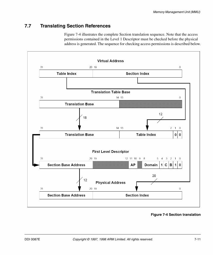
Memory Management Unit (MMU)
7.7 Translating Section References
Figure 7-4 illustrates the complete Section translation sequence. Note that the access permissions contained in the Level 1 Descriptor must be checked before the physical address is generated. The sequence for checking access permissions is described below.
Figure 7-4 Section translation
DDI 0087E Copyright © 1997, 1998 ARM Limited. All rights reserved. 7-11
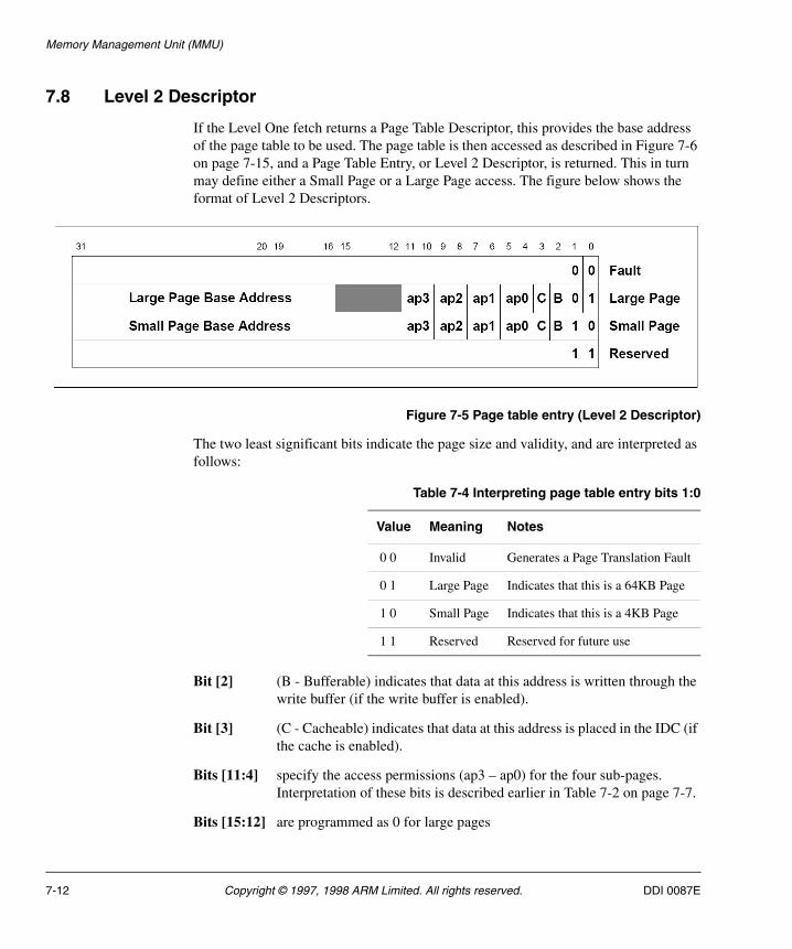
Memory Management Unit (MMU)
7.8 Level 2 Descriptor
If the Level One fetch returns a Page Table Descriptor, this provides the base address of the page table to be used. The page table is then accessed as described in Figure 7-6 on page 7-15, and a Page Table Entry, or Level 2 Descriptor, is returned. This in turn may define either a Small Page or a Large Page access. The figure below shows the format of Level 2 Descriptors.
Figure 7-5 Page table entry (Level 2 Descriptor)
The two least significant bits indicate the page size and validity, and are interpreted as follows:
Bit [2] (B - Bufferable) indicates that data at this address is written through the write buffer (if the write buffer is enabled).
Bit [3] (C - Cacheable) indicates that data at this address is placed in the IDC (if the cache is enabled).
Bits [11:4] specify the access permissions (ap3 – ap0) for the four sub-pages. Interpretation of these bits is described earlier in Table 7-2 on page 7-7.
Bits [15:12] are programmed as 0 for large pages
Table 7-4 Interpreting page table entry bits 1:0
Value Meaning Notes
0 0 Invalid Generates a Page Translation Fault
0 1 Large Page Indicates that this is a 64KB Page
1 0 Small Page Indicates that this is a 4KB Page
1 1 Reserved Reserved for future use
7-12 Copyright © 1997, 1998 ARM Limited. All rights reserved. DDI 0087E
Memory Management Unit (MMU)
Bits [31:12] (small pages)
Bits [31:16] (large pages)
Note Small and large pages are used to form the corresponding bits of the physical address, that is the physical page number. (The page index is derived from the virtual address as illustrated in Figure 7-6 on page 7-15 and Figure 7-7 on page 7-17).
DDI 0087E Copyright © 1997, 1998 ARM Limited. All rights reserved. 7-13
Memory Management Unit (MMU)
7.9 Translating Small Page References
Figure 7-6 on page 7-15 illustrates the complete translation sequence for a 4KB Small Page. Page translation involves one additional step beyond that of a section translation: the Level 1 Descriptor is the Page Table descriptor, and this is used to point to the Level 2 Descriptor, or Page Table Entry. As the access permissions are now contained in the Level 2 Descriptor they must be checked before the physical address is generated. The sequence for checking access permissions is described later.
7-14 Copyright © 1997, 1998 ARM Limited. All rights reserved. DDI 0087E

Memory Management Unit (MMU)
Figure 7-6 Small page translation
DDI 0087E Copyright © 1997, 1998 ARM Limited. All rights reserved. 7-15
Memory Management Unit (MMU)
7.10 Translating Large Page References
Figure 7-7 on page 7-17 illustrates the complete translation sequence for a 64KB Large Page. As the upper four bits of the Page Index and low-order four bits of the Page Table index overlap, each Page Table Entry for a Large Page must be duplicated 16 times (in consecutive memory locations) in the Page Table.
7-16 Copyright © 1997, 1998 ARM Limited. All rights reserved. DDI 0087E
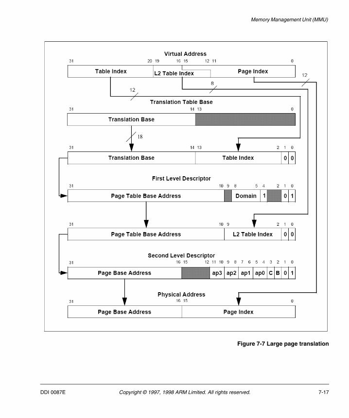
Memory Management Unit (MMU)
Figure 7-7 Large page translation
DDI 0087E Copyright © 1997, 1998 ARM Limited. All rights reserved. 7-17
Memory Management Unit (MMU)
7.11 MMU Faults and CPU Aborts
The MMU generates four types of faults:
• Alignment Fault
• Translation Fault
• Domain Fault
• Permission Fault
In addition, an external abort may be raised on external data access.
The access control mechanisms of the MMU detect the conditions that produce these faults. If a fault is detected as the result of a memory access, the MMU aborts the access and signals the fault condition to the CPU. The MMU is also capable of retaining status and address information about the abort. The CPU recognises two types of abort which are treated differently by the MMU:
• data aborts
• prefetch aborts
If the MMU detects an access violation, it does so before the external memory access takes place, and it therefore inhibits the access. External aborts do not necessarily inhibit the external access, as described in the section on external aborts.
If the ARM720T is operating in fastbus mode an internally aborting access may cause the address on the external address bus to change, even though the external bus cycle has been cancelled. The address that is placed on the bus is the translation of the address that caused the abort, though in the case of a Translation Fault the value of this address is undefined. No memory access is performed to this address.
7-18 Copyright © 1997, 1998 ARM Limited. All rights reserved. DDI 0087E
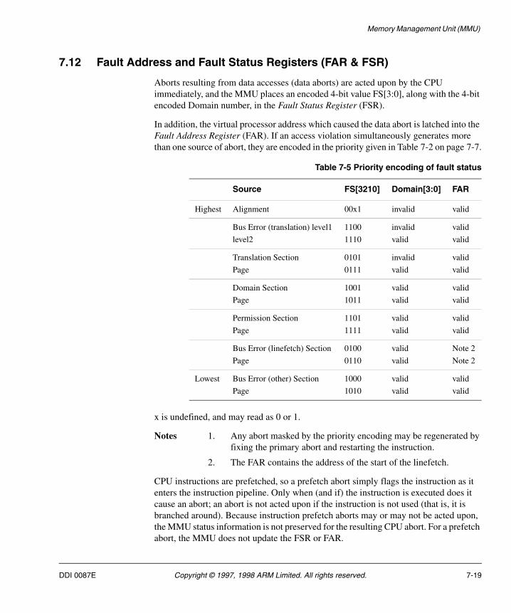
Memory Management Unit (MMU)
7.12 Fault Address and Fault Status Registers (FAR & FSR)
Aborts resulting from data accesses (data aborts) are acted upon by the CPU immediately, and the MMU places an encoded 4-bit value FS[3:0], along with the 4-bit encoded Domain number, in the Fault Status Register (FSR).
In addition, the virtual processor address which caused the data abort is latched into the Fault Address Register (FAR). If an access violation simultaneously generates more than one source of abort, they are encoded in the priority given in Table 7-2 on page 7-7.
x is undefined, and may read as 0 or 1.
Notes 1. Any abort masked by the priority encoding may be regenerated by fixing the primary abort and restarting the instruction.
2. The FAR contains the address of the start of the linefetch.
CPU instructions are prefetched, so a prefetch abort simply flags the instruction as it enters the instruction pipeline. Only when (and if) the instruction is executed does it cause an abort; an abort is not acted upon if the instruction is not used (that is, it is branched around). Because instruction prefetch aborts may or may not be acted upon, the MMU status information is not preserved for the resulting CPU abort. For a prefetch abort, the MMU does not update the FSR or FAR.
Table 7-5 Priority encoding of fault status
Source FS[3210] Domain[3:0] FAR
Highest Alignment 00x1 invalid valid
Bus Error (translation) level1
level2
1100
1110
invalid
valid
valid
valid
Translation Section
Page
0101
0111
invalid
valid
valid
valid
Domain Section
Page
1001
1011
valid
valid
valid
valid
Permission Section
Page
1101
1111
valid
valid
valid
valid
Bus Error (linefetch) Section
Page
0100
0110
valid
valid
Note 2
Note 2
Lowest Bus Error (other) Section
Page
1000
1010
valid
valid
valid
valid
DDI 0087E Copyright © 1997, 1998 ARM Limited. All rights reserved. 7-19
Memory Management Unit (MMU)
The sections that follow describe the various access permissions and controls supported by the MMU and detail how these are interpreted to generate faults.
7-20 Copyright © 1997, 1998 ARM Limited. All rights reserved. DDI 0087E
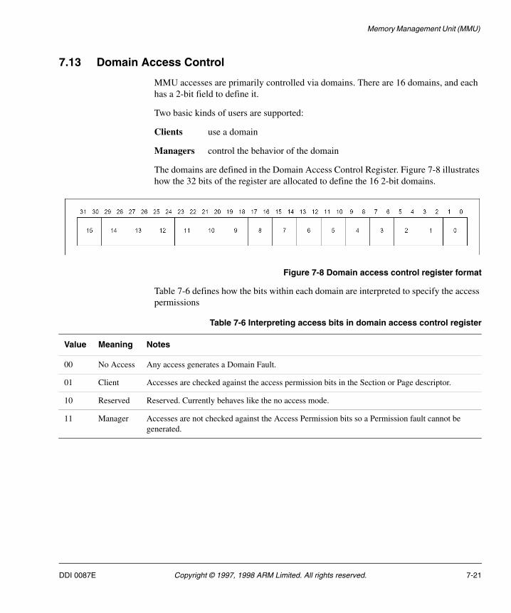
Memory Management Unit (MMU)
7.13 Domain Access Control
MMU accesses are primarily controlled via domains. There are 16 domains, and each has a 2-bit field to define it.
Two basic kinds of users are supported:
Clients use a domain
Managers control the behavior of the domain
The domains are defined in the Domain Access Control Register. Figure 7-8 illustrates how the 32 bits of the register are allocated to define the 16 2-bit domains.
Figure 7-8 Domain access control register format
Table 7-6 defines how the bits within each domain are interpreted to specify the access permissions
Table 7-6 Interpreting access bits in domain access control register
Value Meaning Notes
00 No Access Any access generates a Domain Fault.
01 Client Accesses are checked against the access permission bits in the Section or Page descriptor.
10 Reserved Reserved. Currently behaves like the no access mode.
11 Manager Accesses are not checked against the Access Permission bits so a Permission fault cannot be generated.
DDI 0087E Copyright © 1997, 1998 ARM Limited. All rights reserved. 7-21
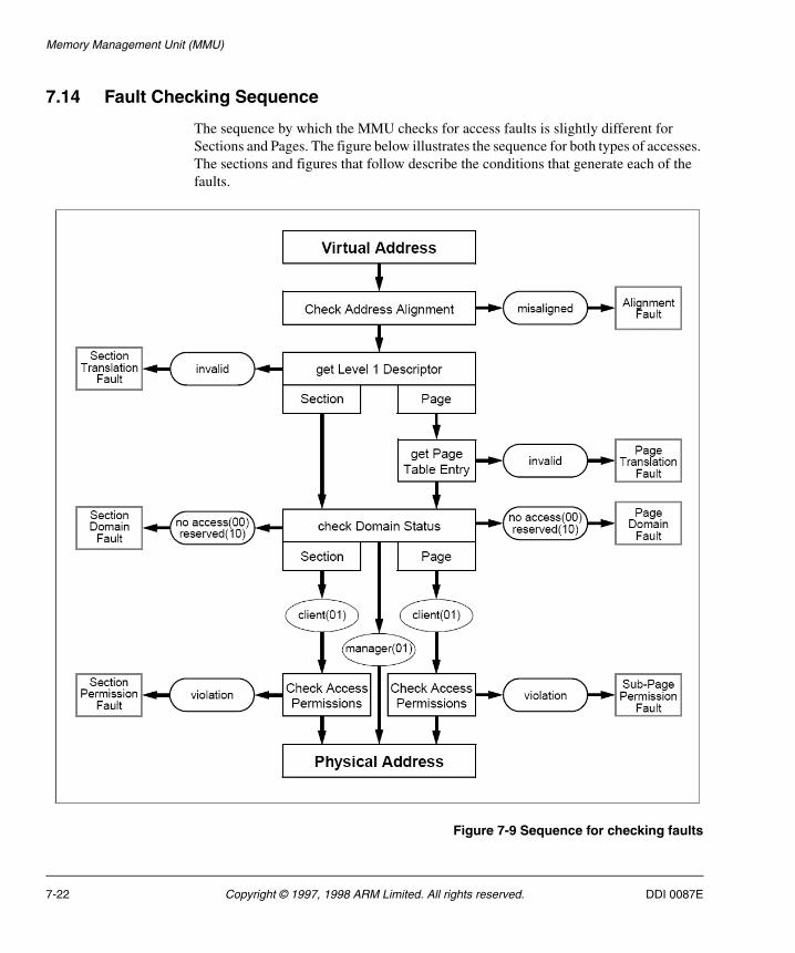
Memory Management Unit (MMU)
7.14 Fault Checking Sequence
The sequence by which the MMU checks for access faults is slightly different for Sections and Pages. The figure below illustrates the sequence for both types of accesses. The sections and figures that follow describe the conditions that generate each of the faults.
Figure 7-9 Sequence for checking faults
7-22 Copyright © 1997, 1998 ARM Limited. All rights reserved. DDI 0087E
Memory Management Unit (MMU)
7.14.1 Alignment fault
If Alignment Fault is enabled (bit 1 in Control Register set), the MMU generates an Alignment Fault on any data word access without a word-aligned address, irrespective of whether the MMU is enabled or not. In other words, if either of virtual address bits [1:0] are not 0, the Alignment Fault is enabled.
An Alignment Fault is not generated on any instruction fetch, nor on any byte access.
Note If the access generates an alignment fault, the access sequence abort without reference to further permission checks.
7.14.2 Translation fault
There are two types of Translation Fault:
section is generated if the Level 1 Descriptor is marked as invalid. This happens if bits[1:0] of the descriptor are both 0 or both 1.
page is generated if the Page Table Entry is marked as invalid. This happens if bits[1:0] of the entry are both 0 or both 1.
7.14.3 Domain fault
There are two types of Domain Fault:
• section
• page
In both cases, the Level 1 Descriptor holds the 4-bit Domain field which selects one of the 16 2-bit domains in the Domain Access Control Register. The two bits of the specified domain are then checked for access permissions as detailed in Table 7-3 on page 7-9.
For a section the domain is checked when the Level 1 Descriptor is returned.
For a page the domain is checked when the Page Table Entry is returned.
If the specified access is either No Access (00) or Reserved (10), either a Section Domain Fault or Page Domain Fault occurs.
DDI 0087E Copyright © 1997, 1998 ARM Limited. All rights reserved. 7-23
Memory Management Unit (MMU)
7.14.4 Permission fault
There are two types of permission fault:
• section
• sub-page
Permission fault is checked at the same time as Domain fault. If the 2-bit domain field returns client (01), the permission access check is invoked as follows:
section If the Level 1 Descriptor defines a section-mapped access, the AP bits of the descriptor define whether or not the access is allowed according to Table 7-3 on page 7-9. Their interpretation depends on the setting of the S bit (Control Register bit 8). If the access is not allowed, a Section Permission fault is generated.
sub-page If the Level 1 Descriptor defines a page-mapped access, the Level 2 Descriptor specifies four access permission fields (ap3...ap0) each corresponding to one quarter of the page.
For small pages:
• ap3 is selected by the top 1KB of the page
• ap0 is selected by the bottom 1KB of the page
For large pages:
• ap3 is selected by the top 16KB of the page
• ap0 is selected by the bottom 16KB of the page.
The selected AP bits are then interpreted in exactly the same way as for a section (see Table 7-3 on page 7-9), the only difference is that the fault generated is a sub-page permission fault.
7-24 Copyright © 1997, 1998 ARM Limited. All rights reserved. DDI 0087E
Memory Management Unit (MMU)
7.15 External Aborts
In addition to the MMU-generated aborts, ARM720T has an external abort pin, BERROR, which may be used to flag an error on an external memory access. However, not all accesses can be aborted in this way, so this pin must be used with great care. The following information describes the restrictions.
The following accesses may be aborted and restarted safely. If any of the following are aborted the external access stops on the next cycle.
• Reads
• Unbuffered writes
• Level 1 Descriptor fetch
• Level 2 Descriptor fetch
• read-lock-write sequence
In the case of a read-lock-write sequence in which the read aborts, the write does not happen.
Cacheable reads (linefetches)
A linefetch may be safely aborted on any word in the transfer.
If an abort occurs during the linefetch, the cache is purged, so it does not contain invalid data.
If the abort happens on a word that has been requested by the ARM720T, it is aborted, otherwise the cache line is purged but program flow is not interrupted. The line is therefore purged under all circumstances.
Buffered writes
Buffered writes cannot be externally aborted. Therefore, the system should be configured such that it does not attempt buffered writes to areas of memory which are capable of flagging an external abort.
Note Areas of memory which can generate an external abort on a location which has previously been read successfully must not be marked a cacheable or unbufferable. This applies to both the MMU page tables and the configuration register. If all writes to an area of memory abort, it is recommended that you mark it as read-only in the MMU, otherwise mark it as uncacheable and unbufferable.
DDI 0087E Copyright © 1997, 1998 ARM Limited. All rights reserved. 7-25
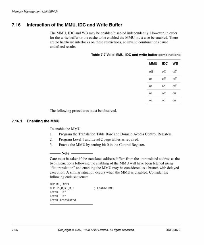
Memory Management Unit (MMU)
7.16 Interaction of the MMU, IDC and Write Buffer
The MMU, IDC and WB may be enabled/disabled independently. However, in order for the write buffer or the cache to be enabled the MMU must also be enabled. There are no hardware interlocks on these restrictions, so invalid combinations cause undefined results
The following procedures must be observed.
7.16.1 Enabling the MMU
To enable the MMU:
1. Program the Translation Table Base and Domain Access Control Registers.
2. Program Level 1 and Level 2 page tables as required.
3. Enable the MMU by setting bit 0 in the Control Register.
Note Care must be taken if the translated address differs from the untranslated address as the two instructions following the enabling of the MMU will have been fetched using “flat translation” and enabling the MMU may be considered as a branch with delayed execution. A similar situation occurs when the MMU is disabled. Consider the following code sequence:
MOV R1, #0x1MCR 15,0,R1,0,0 ; Enable MMUFetch FlatFetch FlatFetch Translated
Table 7-7 Valid MMU, IDC and write buffer combinations
MMU IDC WB
off off off
on off off
on on off
on off on
on on on
7-26 Copyright © 1997, 1998 ARM Limited. All rights reserved. DDI 0087E
Memory Management Unit (MMU)
7.16.2 Disabling the MMU
To disable the MMU:
1. Disable the WB by clearing bit 3 in the Control Register.
2. Disable the IDC by clearing bit 2 in the Control Register.
3. Disable the MMU by clearing bit 0 in the Control Register.
Disabling of all three functions may be done simultaneously.
Note If the MMU is enabled, disabled and subsequently re-enabled, the contents of the TLB are preserved. If these are now invalid, the TLB should be flushed before re-enabling the MMU.
DDI 0087E Copyright © 1997, 1998 ARM Limited. All rights reserved. 7-27
Memory Management Unit (MMU)
7-28 Copyright © 1997, 1998 ARM Limited. All rights reserved. DDI 0087E

Chapter 8 Debug Interface
This chapter describes the ARM720T advanced debug interface.
• Overview on page 8-2
• Debug Systems on page 8-4
• Entering Debug State on page 8-6
• Scan Chains and JTAG Interface on page 8-8
• Reset on page 8-11
• Public Instructions on page 8-12
• Test Data Registers on page 8-16
• ARM7DMT Core Clocks on page 8-25
• Determining the Core and System State on page 8-27
• The PC During Debug on page 8-32
• Priorities and Exceptions on page 8-36
• Scan Interface Timing on page 8-37.
DDI 0087E Copyright © 1997, 1998 ARM Limited. All rights reserved. 8-1
Debug Interface
8.1 Overview
In this chapter ARM7DMT refers to the ARM7TDMI core excluding the EmbeddedICE Macrocell. The ARM7DMT debug interface is based on IEEE Std. 1149.1-1990, “Standard Test Access Port and Boundary-Scan Architecture”. Please refer to this standard for an explanation of the terms used in this chapter and for a description of the TAP controller states.
8.1.1 Debug extensions
ARM7DMT contains hardware extensions for advanced debugging features. These are intended to ease the user’s development of application software, operating systems, and the hardware itself.
The debug extensions allow the core to be stopped either on a given instruction fetch (breakpoint) or data access (watchpoint), or asynchronously by a debug-request. When this happens, ARM7DMT is said to be in debug state. At this point, the core’s internal state and the system’s external state may be examined. Once examination is complete, the core and system state may be restored and program execution resumed.
Debug state
ARM7DMT is forced into debug state either by a request on one of the external debug interface signals, or by an internal functional unit known as EmbeddedICE. Once in debug state, the core isolates itself from the memory system. The core can then be examined while all other system activity continues as normal.
Internal state
ARM7DMT’s internal state is examined via a JTAG-style serial interface, which allows instructions to be serially inserted into the core’s pipeline without using the external data bus so, when in debug state, a store-multiple (STM) could be inserted into the instruction pipeline and this would dump the contents of ARM7DMT’s registers. This data can be serially shifted out without affecting the rest of the system.
8.1.2 Pullup resistors
The IEEE 1149.1 standard effectively requires that TDI and TMS should have internal pullup resistors. In order to minimise static current draw, these resistors are not fitted to ARM7DMT. Accordingly, the four inputs to the test interface (the above three signals plus TCK) must all be driven to good logic levels to achieve normal circuit operation.
8-2 Copyright © 1997, 1998 ARM Limited. All rights reserved. DDI 0087E
Debug Interface
8.1.3 Instruction register
The instruction register is 4 bits in length.
There is no parity bit. The fixed value loaded into the instruction register during the CAPTURE-IR controller state is 0001.
DDI 0087E Copyright © 1997, 1998 ARM Limited. All rights reserved. 8-3
Debug Interface
8.2 Debug Systems
The ARM7DMT forms one component of a debug system that interfaces from the high-level debugging performed by the user to the low-level interface supported by ARM7DMT. Such a system typically has three parts:
The Debug Host This is a computer, for example a PC, running a software debugger such as ARMSD. The debug host allows the user to issue high level commands such as “set breakpoint at location XX”, or “examine the contents of memory from 0x0 to 0x100”
The Protocol Converter
The Debug Host is connected to the ARM7DMT development system via an interface (an RS232, for example). The messages broadcast over this connection must be converted to the interface signals of the ARM7DMT, and this function is performed by the protocol converter.
ARM7DMT ARM7DMT, with hardware extensions to ease debugging, is the lowest level of the system. The debug extensions allow the user to stall the core from program execution, examine its internal state and the state of the memory system, and then resume program execution.
8-4 Copyright © 1997, 1998 ARM Limited. All rights reserved. DDI 0087E
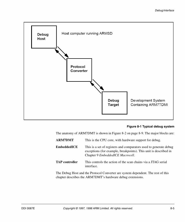
Debug Interface
Figure 8-1 Typical debug system
The anatomy of ARM7DMT is shown in Figure 8-2 on page 8-9. The major blocks are:
ARM7DMT This is the CPU core, with hardware support for debug.
EmbeddedICE This is a set of registers and comparators used to generate debug exceptions (for example, breakpoints). This unit is described in Chapter 9 EmbeddedICE Macrocell.
TAP controller This controls the action of the scan chains via a JTAG serial interface.
The Debug Host and the Protocol Converter are system dependent. The rest of this chapter describes the ARM7DMT’s hardware debug extensions.
DDI 0087E Copyright © 1997, 1998 ARM Limited. All rights reserved. 8-5
Debug Interface
8.3 Entering Debug State
ARM7DMT is forced into debug state after a breakpoint, watchpoint or debug request has occurred. Conditions under which a breakpoint or watchpoint occur can be programmed using EmbeddedICE. Alternatively, external logic can monitor the address and data bus, and flag breakpoints and watchpoints via the BREAKPT pin.
8.3.1 Entering debug state on breakpoint
After an instruction has been breakpointed, the core does not enter debug state immediately. Instructions are marked as being breakpointed as they enter ARM7DMT's instruction pipeline. Thus ARM7DMT only enters debug state when (and if) the instruction reaches the pipeline’s execute stage.
There are two reasons why a breakpointed instruction may not cause ARM7DMT to enter debug state:
• a branch precedes the breakpointed instruction. When the branch is executed, the instruction pipeline is flushed and the breakpoint is cancelled.
• an exception has occurred. Again, the instruction pipeline is flushed and the breakpoint is cancelled. However, the normal way to exit from an exception is to branch back to the instruction that would have executed next. This involves refilling the pipeline, and so the breakpoint can be re-flagged.
When a breakpointed conditional instruction reaches the execute stage of the pipeline, the breakpoint is always taken and ARM7DMT enters debug state, regardless of whether the condition was met.
Breakpointed instructions are not executed. Instead, ARM7DMT enters debug state. Thus, when the internal state is examined, the state before the breakpointed instruction is seen. Once examination is complete, the breakpoint should be removed and program execution restarted from the previously breakpointed instruction.
8.3.2 Entering debug state on watchpoint
Watchpoints occur on data accesses. A watchpoint is always taken, but the core may not enter debug state immediately. In all cases, the current instruction does complete. If this is a multi-word load or store (LDM or STM), many cycles may elapse before the watchpoint is taken.
Watchpoints can be thought of as being similar to data aborts. The difference is that if a data abort occurs, although the instruction completes, all subsequent changes to ARM7DMT’s state are prevented. This allows the cause of the abort to be cured by the abort handler, and the instruction re-executed. In the case of a watchpoint, the
8-6 Copyright © 1997, 1998 ARM Limited. All rights reserved. DDI 0087E

Debug Interface
instruction completes and all changes to the core’s state occur (load data is written into the destination registers, and base writeback occurs). Thus, the instruction does not need to be restarted.
Watchpoints are always taken. If an exception is pending when a watchpoint occurs, the core enters debug state in the mode of that exception.
8.3.3 Entering debug state on debug-request
ARM7DMT may also be forced into debug state on debug request. This can be done either through EmbeddedICE programming (see Chapter 9 EmbeddedICE Macrocell), or by the assertion of the DBGRQ pin. This pin is an asynchronous input and is thus synchronized by logic inside ARM7DMT before it takes effect. Following synchronisation, the core normally enters debug state at the end of the current instruction. However, if the current instruction is a busy-waiting access to a coprocessor, the instruction terminates and ARM7DMT enters debug state immediately (this is similar to the action of nIRQ and nFIQ).
DDI 0087E Copyright © 1997, 1998 ARM Limited. All rights reserved. 8-7
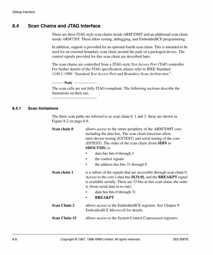
Debug Interface
8.4 Scan Chains and JTAG Interface
There are three JTAG style scan chains inside ARM7DMT and an additional scan chain inside ARM720T. These allow testing, debugging, and EmbeddedICE programming.
In addition, support is provided for an optional fourth scan chain. This is intended to be used for an external boundary scan chain around the pads of a packaged device. The control signals provided for this scan chain are described later.
The scan chains are controlled from a JTAG-style Test Access Port (TAP) controller. For further details of the JTAG specification, please refer to IEEE Standard 1149.1-1990 “Standard Test Access Port and Boundary-Scan Architecture”.
Note The scan cells are not fully JTAG-compliant. The following sections describe the limitations on their use.
8.4.1 Scan limitations
The three scan paths are referred to as scan chain 0, 1 and 2: these are shown in Figure 8-2 on page 8-9.
Scan chain 0 allows access to the entire periphery of the ARM7DMT core, including the data bus. The scan chain functions allow inter-device testing (EXTEST) and serial testing of the core (INTEST). The order of the scan chain (from SDIN to SDOUTMS) is:
• data bus bits 0 through 3
• the control signals
• the address bus bits 31 through 0
Scan chain 1 is a subset of the signals that are accessible through scan chain 0. Access to the core’s data bus D[31:0], and the BREAKPT signal is available serially. There are 33 bits in this scan chain; the order is (from serial data in to out):
• data bus bits 0 through 31
• BREAKPT
Scan Chain 2 allows access to the EmbeddedICE registers. See Chapter 9 EmbeddedICE Macrocell for details.
Scan Chain 15 allows access to the System Control Coprocessor registers.
8-8 Copyright © 1997, 1998 ARM Limited. All rights reserved. DDI 0087E
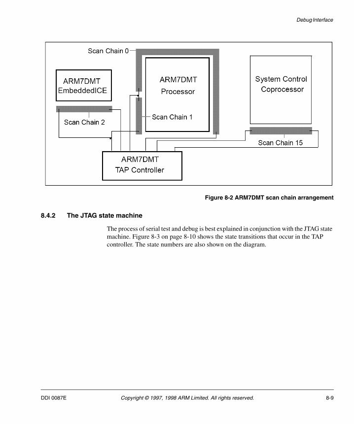
Debug Interface
Figure 8-2 ARM7DMT scan chain arrangement
8.4.2 The JTAG state machine
The process of serial test and debug is best explained in conjunction with the JTAG state machine. Figure 8-3 on page 8-10 shows the state transitions that occur in the TAP controller. The state numbers are also shown on the diagram.
DDI 0087E Copyright © 1997, 1998 ARM Limited. All rights reserved. 8-9
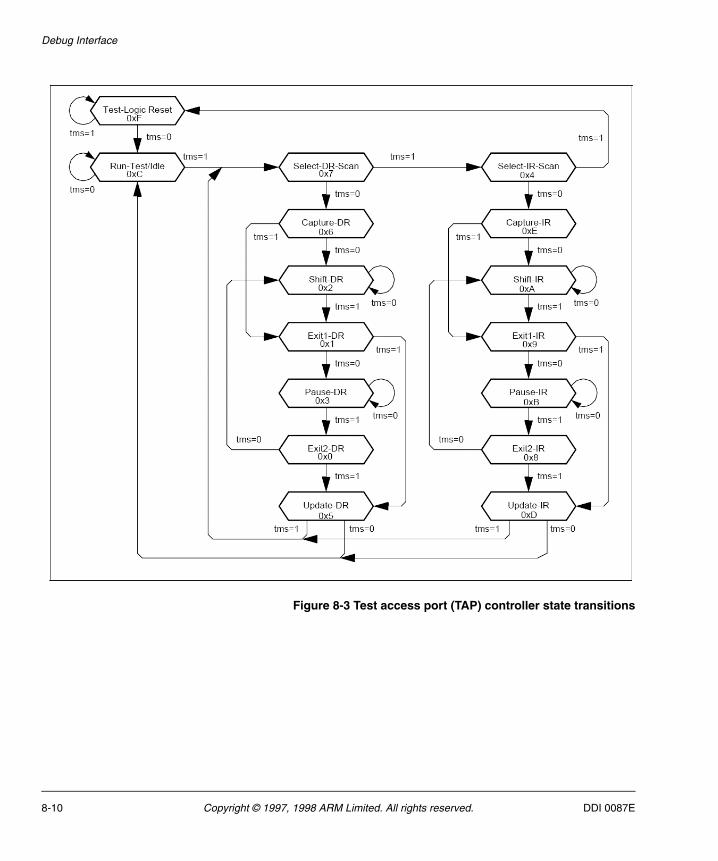
Debug Interface
Figure 8-3 Test access port (TAP) controller state transitions
8-10 Copyright © 1997, 1998 ARM Limited. All rights reserved. DDI 0087E
Debug Interface
8.5 Reset
The boundary-scan interface includes a state-machine controller (the TAP controller). In order to force the TAP controller into the correct state after power-up of the device, a reset pulse must be applied to the nTRST signal.
If the boundary scan interface is to be used, nTRST must be driven LOW, and then HIGH again. If the boundary scan interface is not to be used, the nTRST input may be tied permanently LOW.
Note A clock on TCK is not necessary to reset the device.
The action of reset is as follows:
1. System mode is selected (the boundary scan chain cells do not intercept any of the signals passing between the external system and the core).
2. The IDCODE instruction is selected. If the TAP controller is put into the Shift-DR state and TCK is pulsed, the contents of the ID register is clocked out of TDO.
DDI 0087E Copyright © 1997, 1998 ARM Limited. All rights reserved. 8-11
Debug Interface
8.6 Public Instructions
The public instructions are listed below. In the descriptions that follow, TDI and TMS are sampled on the rising edge of TCK and all output transitions on TDO occur as a result of the falling edge of TCK.
EXTEST 0000 places the selected scan chain in test mode. This instruction connects the selected scan chain between TDI and TDO.
When the instruction register is loaded with EXTEST, all the scan cells are placed in their test mode of operation.
CAPTURE-DR Inputs from the system logic and outputs from the output scan cells to the system are captured by the scan cells.
SHIFT-DR The previously captured test data is shifted out of the scan chain via TDO, while new test data is shifted in via the TDI input. This data is applied immediately to the system logic and system pins.
SCAN_N 0010 connects the Scan Path Select Register between TDI and TDO. On reset, scan chain 3 is selected by default. The scan path select register is 4 bits long in this implementation, although no finite length is specified.
CAPTURE-DR The fixed value 1000 is loaded into the register.
SHIFT-DR The ID number of the desired scan path is shifted into the scan path select register
UPDATE-DR The scan register of the selected scan chain is connected between TDI and TDO, and remains connected until a subsequent SCAN_N instruction is issued.
INTEST 1100 places the selected scan chain test mode. This instruction connects the selected scan chain between TDI and TDO.
When the instruction register is loaded with this instruction, all the scan cells are placed in their test mode of operation.
Single-step operation is possible using the INTEST instruction.
CAPTURE-DR The value of the data applied from the core logic to the output scan cells, and the value of the data applied from the system logic to the input scan cells is captured.
8-12 Copyright © 1997, 1998 ARM Limited. All rights reserved. DDI 0087E
Debug Interface
SHIFT-DR The previously captured test data is shifted out of the scan chain via the TDO pin, while new test data is shifted in via the TDI pin.
IDCODE 1110 connects the device identification register (or ID register) between TDI and TDO. The ID register is a 32-bit register that allows the manufacturer, part number and version of a component to be determined through the TAP. See ARM7DMT device identification (ID) code register on page 8-16 for the details of the ID register format.
When the instruction register is loaded with this instruction, all the scan cells are placed in their normal (system) mode of operation.
CAPTURE-DR The device identification code is captured by the ID register
SHIFT-DR The previously captured device identification code is shifted out of the ID register via the TDO pin, while data is shifted in via the TDI pin into the ID register.
UPDATE-DR The ID register is unaffected.
BYPASS 1111 connects a 1-bit shift register (the bypass register) between TDI and TDO.
When this instruction is loaded into the instruction register, all the scan cells are placed in their normal (system) mode of operation. This instruction has no effect on the system pins.
Note All unused instruction codes default to the bypass instruction.
CAPTURE-DR A logic 0 is captured by the bypass register.
SHIFT-DR Test data is shifted into the bypass register via TDI and out via TDO after a delay of one TCK cycle. Note that the first bit shifted out is a zero.
UPDATE-DR The bypass register is not affected.
CLAMP 0101 connects a 1-bit shift register (the bypass register) between TDI and TDO.
DDI 0087E Copyright © 1997, 1998 ARM Limited. All rights reserved. 8-13
Debug Interface
When this instruction is loaded into the instruction register, the state of all the output signals is defined by the values previously loaded into the currently loaded scan chain.
Note This instruction should only be used when scan chain 0 is the
currently selected scan chain.
CAPTURE-DR A logic 0 is captured by the bypass register.
SHIFT-DR Test data is shifted into the bypass register via TDI and out via TDO after a delay of one TCK cycle. Note that the first bit shifted out is a zero.
UPDATE-DR The bypass register is not affected.
HIGHZ 0111 connects a 1-bit shift register (the bypass register) between TDI and TDO.
When this instruction is loaded into the instruction register, the Address bus, A[31:0], the data bus, D[31:0], plus nRW, nOPC, LOCK, MAS[1:0], and nTRANS are all driven to the high impedance state and the external HIGHZ signal is driven HIGH. This is as if the signal TBE had been driven LOW.
CAPTURE-DR A logic 0 is captured by the bypass register.
SHIFT-DR Test data is shifted into the bypass register via TDI and out via TDO after a delay of one TCK cycle. Note that the first bit shifted out is a zero.
UPDATE-DR The bypass register is not affected.
CLAMPZ 1001 connects a 1-bit shift register (the bypass register) between TDI and TDO.
When this instruction is loaded into the instruction register, all the 3-state outputs (as described above) are placed in their inactive state, but the data supplied to the outputs is derived from the scan cells. The purpose of this instruction is to ensure that, during production test, each output can be disabled when its data value is either a logic 0 or a logic 1.
CAPTURE-DR A logic 0 is captured by the bypass register.
8-14 Copyright © 1997, 1998 ARM Limited. All rights reserved. DDI 0087E
Debug Interface
SHIFT-DR Test data is shifted into the bypass register via TDI and out via TDO after a delay of one TCK cycle. Note that the first bit shifted out will be a zero.
UPDATE-DR The bypass register is not affected.
RESTART 0100 restarts the processor on exit from debug state. It connects the bypass register between TDI and TDO and the TAP controller behaves as if the bypass instruction had been loaded. The processor resynchronizes back to the memory system once the RUN-TEST/IDLE state is entered.
SAMPLE/PRELOAD 0011
Note This instruction is included for production test only, and should
never be used.
DDI 0087E Copyright © 1997, 1998 ARM Limited. All rights reserved. 8-15
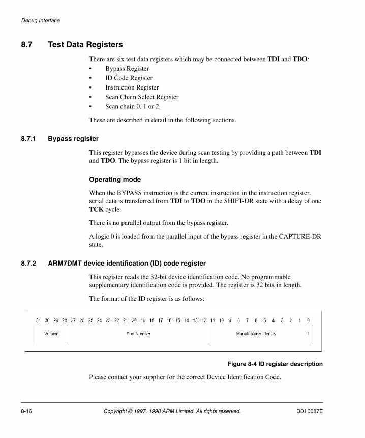
Debug Interface
8.7 Test Data Registers
There are six test data registers which may be connected between TDI and TDO:
• Bypass Register
• ID Code Register
• Instruction Register
• Scan Chain Select Register
• Scan chain 0, 1 or 2.
These are described in detail in the following sections.
8.7.1 Bypass register
This register bypasses the device during scan testing by providing a path between TDI and TDO. The bypass register is 1 bit in length.
Operating mode
When the BYPASS instruction is the current instruction in the instruction register, serial data is transferred from TDI to TDO in the SHIFT-DR state with a delay of one TCK cycle.
There is no parallel output from the bypass register.
A logic 0 is loaded from the parallel input of the bypass register in the CAPTURE-DR state.
8.7.2 ARM7DMT device identification (ID) code register
This register reads the 32-bit device identification code. No programmable supplementary identification code is provided. The register is 32 bits in length.
The format of the ID register is as follows:
Figure 8-4 ID register description
Please contact your supplier for the correct Device Identification Code.
8-16 Copyright © 1997, 1998 ARM Limited. All rights reserved. DDI 0087E
Debug Interface
Operating mode
When the IDCODE instruction is current, the ID register is selected as the serial path between TDI and TDO.
There is no parallel output from the ID register.
The 32-bit device identification code is loaded into the ID register from its parallel inputs during the CAPTURE-DR state.
8.7.3 Instruction register
This register changes the current TAP instruction. The register is 4 bits in length
Operating mode
When in the SHIFT-IR state, the instruction register is selected as the serial path between TDI and TDO.
During the CAPTURE-IR state, the value 0001 binary is loaded into this register. This is shifted out during SHIFT-IR least significant bit (lsb) first, while a new instruction is shifted in (lsb first).
During the UPDATE-IR state, the value in the instruction register becomes the current instruction.
On reset, IDCODE becomes the current instruction.
8.7.4 Scan chain select register
This register changes the current active scan chain. The register is 4 bits in length.
Operating mode
After SCAN_N has been selected as the current instruction, when in the SHIFT-DR state, the Scan Chain Select Register is selected as the serial path between TDI and TDO.
During the CAPTURE-DR state, the value 1000 binary is loaded into this register. This is shifted out during SHIFT-DR (lsb first), while a new value is shifted in (lsb first).
During the UPDATE-DR state, the value in the register selects a scan chain to become the currently active scan chain. All further instructions, such as INTEST, then apply to that scan chain.
DDI 0087E Copyright © 1997, 1998 ARM Limited. All rights reserved. 8-17
Debug Interface
The currently selected scan chain only changes when a SCAN_N instruction is executed, or a reset occurs. On reset, scan chain 3 is selected as the active scan chain.
The number of the currently selected scan chain is reflected on the SCREG[3:0] outputs. The TAP controller may be used to drive external scan chains in addition to those within the ARM7DMT macrocell. The external scan chain must be assigned a number and control signals for it can be derived from SCREG[3:0], IR[3:0], TAPSM[3:0], TCK1 and TCK2.
The list of scan chain numbers allocated by ARM are shown in Table 8-1. An external scan chain may take any other number. The serial data stream to be applied to the external scan chain is made present on SDINBS, the serial data back from the scan chain must be presented to the TAP controller on the SDOUTBS input.
The scan chain present between SDINBS and SDOUTBS will be connected between TDI and TDO whenever scan chain 3 is selected, or when any of the unassigned scan chain numbers is selected. If there is more than one external scan chain, a multiplexer must be built externally to apply the desired scan chain output to SDOUTBS. The multiplexer can be controlled by decoding SCREG[3:0].
8.7.5 Overview of scan chains 0,1, 2 and 15
These allow serial access to the core logic, and to EmbeddedICE for programming purposes. They are described in detail below.
Scan chains 0 and 1 allow access to the processor core for test and debug. They have the following length:
Scan chain 0 105 bits
Table 8-1 Scan chain number allocation
Scan Chain Number Function
0 Macrocell scan test
1 Debug
2 EmbeddedICE programming
3 External boundary scan
4 Reserved
8 Reserved
15 System Control Coprocessor
8-18 Copyright © 1997, 1998 ARM Limited. All rights reserved. DDI 0087E
Debug Interface
Scan chain 1 33 bits
Each scan chain cell is fairly simple, and consists of a serial register and a multiplexer. The scan cells perform two basic functions:
capture For input cells, the capture stage involves copying the value of the system input to the core into the serial register.
For output cells, capture involves placing the value of a core’s output into the serial register.
shift For input cells, during shift, this value is output serially. The value applied to the core from an input cell is either the system input or the contents of the serial register, and this is controlled by the multiplexer.
For output cells, during shift, this value is serially output as before. The value applied to the system from an output cell is either the core output, or the contents of the serial register.
DDI 0087E Copyright © 1997, 1998 ARM Limited. All rights reserved. 8-19

Debug Interface
Figure 8-5 Input scan cell
All the control signals for the scan cells are generated internally by the TAP controller. The action of the TAP controller is determined by the current instruction, and the state of the TAP state machine. This is described in the following section.
Operating modes
The scan chains have three basic modes of operation. These are selected by the various TAP controller instructions.
SYSTEM mode The scan cells are idle. System data is applied to inputs, and core outputs are applied to the system.
INTEST mode The core is internally tested. The data serially scanned in is applied to the core, and the resulting outputs are captured in the output cells and scanned out.
8-20 Copyright © 1997, 1998 ARM Limited. All rights reserved. DDI 0087E

Debug Interface
EXTEST mode Data is scanned onto the core's outputs and applied to the external system. System input data is captured in the input cells and then shifted out.
Note The scan cells are not fully JTAG-compliant in that they do not have an Update stage. Therefore, while data is being moved around the scan chain, the contents of the scan cell is not isolated from the output. Thus the output from the scan cell to the core or to the external system could change on every scan clock.
This does not affect ARM7DMT because its internal state does not change until it is clocked. However, the rest of the system needs to be aware that every output could change asynchronously as data is moved around the scan chain. External logic must ensure that this does not harm the rest of the system.
8.7.6 Scan chain 0
Scan chain 0 is intended primarily for inter-device testing (EXTEST), and testing the core (INTEST). Scan chain 0 is selected via the SCAN_N instruction.
Serial testing the core
INTEST allows serial testing of the core. The TAP Controller must be placed in INTEST mode after scan chain 0 has been selected.
• During CAPTURE-DR, the current outputs from the core’s logic are captured in the output cells.
• During SHIFT-DR, this captured data is shifted out while a new serial test pattern is scanned in, thus applying known stimuli to the inputs.
• During RUN-TEST/IDLE, the core is clocked. Normally, the TAP controller should only spend 1 cycle in RUN-TEST/IDLE.
The whole operation may then be repeated.
See ARM7DMT Core Clocks on page 8-25 for details of the core’s clocks during test and debug.
DDI 0087E Copyright © 1997, 1998 ARM Limited. All rights reserved. 8-21

Debug Interface
Inter-device testing
EXTEST allows inter-device testing, which is useful for verifying the connections between devices on a circuit board. The TAP Controller must be placed in EXTEST mode after scan chain 0 has been selected.
• During CAPTURE-DR, the current inputs to the core's logic from the system are captured in the input cells.
• During SHIFT-DR, this captured data is shifted out while a new serial test pattern is scanned in, thus applying known values on the core’s outputs.
• During UPDATE-DR, the value shifted into the data bus D[31:0] scan cells appears on the outputs. For all other outputs, the value appears as the data is shifted round.
Note During RUN-TEST/IDLE, the core is not clocked.
The operation may then be repeated. The ordering of signals on scan chain 0 is outlined in Table 8-3 on page 8-39.
8.7.7 Scan chain 1
The primary use for scan chain 1 is for debugging, although it can be used for EXTEST on the data bus. Scan chain 1 is selected via the SCAN_N TAP Controller instruction. Debugging is similar to INTEST, and the procedure described above for scan chain 0 should be followed.
Scan chain length and purpose
This scan chain is 33 bits long—32 bits for the data value, plus the scan cell on the BREAKPT core input. This 33rd bit serves four purposes:
1. Under normal INTEST test conditions, it allows a known value to be scanned into the BREAKPT input.
2. During EXTEST test conditions, the value applied to the BREAKPT input from the system can be captured.
3. While debugging, the value placed in the 33rd bit determines whether ARM7DMT synchronizes back to system speed before executing the instruction. See System-speed access on page 8-34 for further details.
8-22 Copyright © 1997, 1998 ARM Limited. All rights reserved. DDI 0087E
Debug Interface
4. After ARM7DMT has entered debug state, the first time this bit is captured and scanned out, its value tells the debugger whether the core entered debug state due to a breakpoint (bit 33 LOW), or a watchpoint (bit 33 HIGH).
8.7.8 Scan chain 2
This scan chain allows EmbeddedICE's registers to be accessed. The scan chain is 38 bits in length.
The order of the scan chain, from TDI to TDO is:
• read/write
• register address bits 4 to 0
• data value bits 31 to 0
See Figure 9-2 on page 9-6 for more information.
To access this serial register, scan chain 2 must first be selected via the SCAN_N TAP controller instruction. The TAP controller must then be place in INTEST mode.
• No action is taken during CAPTURE-DR.
• During SHIFT-DR, a data value is shifted into the serial register. Bits 32 to 36 specify the address of the EmbeddedICE register to be accessed.
• During UPDATE-DR, this register is either read or written depending on the value of bit 37 (0 = read). Refer to Chapter 9 EmbeddedICE Macrocell for further details.
8.7.9 Scan chain 3
This scan chain allows ARM7DMT to control an external boundary scan chain. Scan chain 3 is provided so that an optional external boundary scan chain may be controlled via ARM7DMT. Typically, this would be used for a scan chain around the pad ring of a packaged device. Its length is user-defined.
The following control signals are provided. These are generated only when scan chain 3 has been selected. These outputs are inactive at all other times.
DRIVEBS This would be used to switch the scan cells from system mode to test mode. This signal is asserted whenever either the INTEST, EXTEST, CLAMP or CLAMPZ instruction is selected.
PCLKBS This is an update clock, generated in the UPDATE-DR state. Typically the value scanned into a chain would be transferred to the cell output on the rising edge of this signal.
DDI 0087E Copyright © 1997, 1998 ARM Limited. All rights reserved. 8-23
Debug Interface
ICAPCLKBS ECAPCLKBS
These are capture clocks used to sample data into the scan cells during INTEST and EXTEST respectively. These clocks are generated in the CAPTURE-DR state.
SHCLKBS SHCLK2BS
These are non-overlapping clocks generated in the SHIFT-DR state used to clock the master and slave element of the scan cells respectively. When the state machine is not in the SHIFT-DR state, both these clocks are LOW.
nHIGHZ This signal may be used to drive the outputs of the scan cells to the high impedance state. This signal is driven LOW when the HIGHZ instruction is loaded into the instruction register, and HIGH at all other times.
External scan chains
In addition to the above control outputs, the following are provided for use when an external scan chain is in use:
SDINBS output should be connected to the serial data input.
SDOUTBS input should be connected to the serial data output.
8.7.10 Scan chain 15
This scan chain allows access to the System Control Coprocessor registers. Scan chain 15 is selected via the SCAN_N Tap controller instruction. This scan chain is 33 bits long—32 bits for the data/instruction value plus an additional bit which identifies the value as instruction (1) or data (0). This scan chain should only be used during INTEST. The order of the scan chain from TDI to TDO is:
• CPData [0:31]
• Instruction/Data Flag
8-24 Copyright © 1997, 1998 ARM Limited. All rights reserved. DDI 0087E
Debug Interface
8.8 ARM7DMT Core Clocks
ARM7DMT has two clocks:
• the memory clock, MCLK, generated by the ARM720T.
• an internally TCK-generated clock, DCLK.
During normal operation, the core is clocked by MCLK, and internal logic holds DCLK LOW.
There are two cases in which the clocks switch:
• during debugging
• during testing
8.8.1 Clock switch during debug
When ARM7DMT is in the debug state, the core is clocked by DCLK under the control of the TAP state machine, and MCLK may free run. The selected clock is output on the signal ECLK for use by the external system.
Note When the CPU core is being debugged and is running from DCLK, nWAIT has no effect.
When ARM7DMT enters debug state, it must switch from MCLK to DCLK. This is handled automatically by logic in the ARM7DMT. On entry to debug state, ARM7DMT asserts DBGACK in the HIGH phase of MCLK. The switch between the two clocks occurs on the next falling edge of MCLK. This is shown in Figure 8-6 on page 8-26.
DDI 0087E Copyright © 1997, 1998 ARM Limited. All rights reserved. 8-25
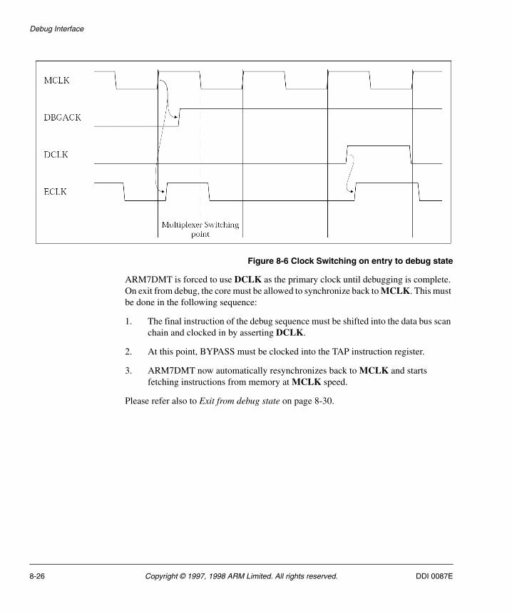
Debug Interface
Figure 8-6 Clock Switching on entry to debug state
ARM7DMT is forced to use DCLK as the primary clock until debugging is complete. On exit from debug, the core must be allowed to synchronize back to MCLK. This must be done in the following sequence:
1. The final instruction of the debug sequence must be shifted into the data bus scan chain and clocked in by asserting DCLK.
2. At this point, BYPASS must be clocked into the TAP instruction register.
3. ARM7DMT now automatically resynchronizes back to MCLK and starts fetching instructions from memory at MCLK speed.
Please refer also to Exit from debug state on page 8-30.
8-26 Copyright © 1997, 1998 ARM Limited. All rights reserved. DDI 0087E

Debug Interface
8.9 Determining the Core and System State
When ARM7DMT is in debug state, the core and system’s state may be examined. This is done by forcing load and store multiples into the instruction pipeline.
ARM or THUMB state
Before the core and system state can be examined, the debugger must first determine whether the processor was in THUMB or ARM state when it entered debug. This is achieved by examining bit 4 of EmbeddedICE’s Debug Status Register. If this is HIGH, the core was in THUMB state when it entered debug.
8.9.1 Determining the core’s state
If the processor has entered debug state from THUMB state, the simplest course of action is for the debugger to force the core back into ARM state. Once this is done, the debugger can always execute the same sequence of instructions to determine the processor's state.
While in debug state, only the following instructions may legally be scanned into the instruction pipeline for execution:
• all data-processing instructions, except TEQP
• all load, store, load multiple and store multiple instructions
• MSR and MRS
Moving to ARM state
To force the processor into ARM state, the following sequence of THUMB instructions should be executed on the core:
STR R0, [R0] ; Save R0 before useMOV R0, PC ; Copy PC into R0STR R0, [R0] ; Now save the PC in R0BX PC ; Jump into ARM stateMOV R8, R8 ; NOPMOV R8, R8 ; NOP
As all THUMB instructions are only 16 bits long, the simplest course of action when shifting them into scan chain 1 is to repeat the instruction twice.
For example, the encoding for BX R0 is 0x4700. Therefore, if 0x47004700 is shifted into scan chain 1, the debugger does not have to keep track of which half of the bus the processor expects to read the data from.
DDI 0087E Copyright © 1997, 1998 ARM Limited. All rights reserved. 8-27
Debug Interface
From this point on, the processor's state can be determined by the sequences of ARM instructions described below.
In ARM state
Once the processor is in ARM state, the first instruction executed would typically be:
STM R0, {R0-R15}
This makes the contents of the registers visible on the data bus. These values can then be sampled and shifted out.
Note The above use of R0 as the base register for STM is for illustration only: any register could be used.
Accessing banked registers
After determining the values in the current bank of registers, it may be desirable to access the banked registers. This can only be done by changing mode. Normally, a mode change may only occur if the core is already in a privileged mode. However, while in debug state, a mode change from any mode into any other mode may occur.
Note The debugger must restore the original mode before exiting debug state.
For example, assume that the debugger had been asked to return the state of the USER and FIQ mode registers, and debug state was entered in supervisor mode.
The instruction sequence could be:
STM R0, {R0-R15} ; Save current registersMRS R0, CPSRSTR R0, R0 ; Save CPSR to determine current modeBIC R0, 0x1F ; Clear mode bitsORR R0, 0x10 ; Select user modeMSR CPSR, R0 ; Enter USER modeSTM R0, {R13,R14} ; Save register not previously visibleORR R0, 0x01 ; Select FIQ modeMSR CPSR, R0 ; Enter FIQ modeSTM R0, {R8-R14} ; Save banked FIQ registers
8-28 Copyright © 1997, 1998 ARM Limited. All rights reserved. DDI 0087E
Debug Interface
All these instructions are said to execute at debug speed. Debug speed is much slower than system speed because between each core clock, 33 scan clocks occur in order to shift in an instruction, or shift out data. Executing instructions more slowly than usual is fine for accessing the core’s state because ARM7DMT is fully static. However, this same method cannot be used for determining the state of the rest of the system.
8.9.2 Determining system state
In order to meet the dynamic timing requirements of the memory system, any attempt to access system state must occur synchronously with it. Thus, ARM7DMT must be forced to synchronize back to system speed. This is controlled by the 33rd bit of scan chain 1.
Any instruction may be placed in scan chain 1 with bit 33 (the BREAKPT bit) LOW. This instruction is then executed at debug speed. To execute an instruction at system speed, the instruction prior to it must be scanned into scan chain 1 with bit 33 set HIGH.
After the system speed instruction has been scanned into the data bus and clocked into the pipeline, the BYPASS instruction must be loaded into the TAP controller. This makes the ARM7DMT automatically synchronize back to MCLK (the system clock), executes the instruction at system speed, and then re-enters debug state and switches itself back to the internally generated DCLK. When the instruction has completed, DBGACK is HIGH and the core will have switched back to DCLK. At this point, INTEST can be selected in the TAP controller, and debugging can resume.
In order to determine that a system speed instruction has completed, the debugger must look at both DBGACK and nMREQ. In order to access memory, ARM7DMT drives nMREQ LOW after it has synchronized back to system speed. This transition is used by the memory controller to arbitrate whether ARM7DMT can have the bus in the next cycle. If the bus is not available, ARM7DMT may have its clock stalled indefinitely.
Therefore, the only way to tell that the memory access has completed, is to examine the state of both nMREQ and DBGACK. When both are HIGH, the access has completed. Usually, the debugger would be using EmbeddedICE to control debugging, and by reading EmbeddedICE’s status register, the state of nMREQ and DBGACK can be determined. Refer to Chapter 9 EmbeddedICE Macrocell for more details.
By the use of system speed load multiples and debug speed store multiples, the state of the system’s memory can be fed back to the debug host.
Restrictions
There are restrictions on which instructions may have the 33rd bit set. The only valid instructions where this bit can be set are:
• loads
DDI 0087E Copyright © 1997, 1998 ARM Limited. All rights reserved. 8-29
Debug Interface
• stores
• load multiple
• store multiple
See also Exit from debug state.
When ARM7DMT returns to debug state after a system speed access, bit 33 of scan chain 1 is set HIGH. This gives the debugger information about why the core entered debug state the first time this scan chain is read.
8.9.3 Determining system control coprocessor state
In order to access the System Control Coprocessor registers, debug state must be entered by a breakpoint, watchpoint or debug request. This ensures that the ARM7DMT core stops execution of code which may be dependent on the System Control Coprocessor.
Scan Chain 15 can then be selected via the SCAN_N instruction.
Instructions may then be scanned down the scan chain as if being executed from the ARM7DMT core. As the ARM7DMT is idle while Scan Chain 15 is being accessed, it is necessary to provide the register data via the scan chain. The instruction prior to the data must have the instruction/data flag cleared.
The data operation requires an additional clock from the TAP controller. This may be achieved by remaining in the RUN-TEST-IDLE state for an additional TCK cycle.
8.9.4 Exit from debug state
Leaving debug state involves:
1. Restoring ARM7DMT’s internal state.
2. Branching to the next instruction to be executed.
3. Synchronising back to MCLK.
After restoring internal state, a branch instruction must be loaded into the pipeline. See The PC During Debug on page 8-32 for details on calculating the branch.
Bit 33 of scan chain 1 is used to force ARM7DMT to resynchronize back to MCLK. The penultimate instruction of the debug sequence is scanned in with bit 33 set HIGH. The final instruction of the debug sequence is the branch, and this is scanned in with bit 33 LOW. The core is then clocked to load the branch into the pipeline. Now, the RESTART instruction is selected in the TAP controller.
8-30 Copyright © 1997, 1998 ARM Limited. All rights reserved. DDI 0087E
Debug Interface
When the state machine enters the RUN-TEST/IDLE state, the scan chain reverts back to system mode and clock resynchronization to MCLK occurs within ARM7DMT. ARM7DMT then resumes normal operation, fetching instructions from memory. This delay, until the state machine is in the RUN-TEST/IDLE state, allows conditions to be set up in other devices in a multiprocessor system without taking immediate effect. Then, when the RUN-TEST/IDLE state is entered, all the processors resume operation simultaneously.
DDI 0087E Copyright © 1997, 1998 ARM Limited. All rights reserved. 8-31
Debug Interface
8.10 The PC During Debug
So that ARM7DMT may be forced to branch back to the place at which program flow was interrupted by debug, the debugger must keep track of what happens to the PC.
There are five cases:
• breakpoint
• watchpoint
• watchpoint when another exception occurs
• debug request
• system-speed access
8.10.1 Breakpoint
Entry to the debug state from a breakpoint advances the PC by 4 addresses, or 16 bytes. Each instruction executed in debug state advances the PC by 1 address, or 4 bytes. The normal way to exit from debug state after a breakpoint is to remove the breakpoint, and branch back to the previously breakpointed address.
For example, if ARM7DMT entered debug state from a breakpoint set on a given address and two debug-speed instructions were executed, a branch of -7 addresses must occur (4 for debug entry, +2 for the instructions, +1 for the final branch).
The following sequence shows the data scanned into scan chain 1. This is msb (most signifigant bit) first, and so the first digit is the value placed in the BREAKPT bit, followed by the instruction data:
0 E0802000 ; ADD R2, R0, R01 E1826001 ; ORR R6, R2, R10 EAFFFFF9 ; B -7 (2’s complement)
Once in debug state, a minimum of two instructions must be executed before the branch, although these may both be NOPs, for example:
MOV R0, R0
For small branches, the final branch could be replaced by a subtract with the PC as the destination:
SUB PC, PC, #28
8-32 Copyright © 1997, 1998 ARM Limited. All rights reserved. DDI 0087E

Debug Interface
8.10.2 Watchpoint
Returning to program execution after entering debug state from a watchpoint is done in the same way as the procedure described above. Debug entry adds 4 addresses to the PC, and every instruction adds one address. The difference is that because the instruction that caused the watchpoint has executed, the program returns to the next instruction.
8.10.3 Watchpoint with another exception
If a watchpointed access simultaneously causes a data abort, ARM7DMT enters debug state in abort mode. Entry into debug is held off until the core has changed into abort mode, and fetched the instruction from the abort vector.
A similar sequence is followed when an interrupt, or any other exception, occurs during a watchpointed memory access. ARM7DMT enters debug state in the exception’s mode, and so the debugger must check to see whether this happened. The debugger can deduce whether an exception occurred by looking at the current and previous mode (in the CPSR and SPSR), and the value of the PC. If an exception did take place, the user should be given the choice of whether to service the exception before debugging.
Exiting from debug state
Exiting debug state if an exception occurred is slightly different from the other cases.
Here, entry to debug state causes the PC to be incremented by three addresses rather than four, and this must be taken into account in the return branch calculation. For example, suppose that an abort occurred on a watchpointed access and ten instructions had been executed to determine this. The following sequence could be used to return to program execution:
0 E1A00000 ; MOV R0, R01 E1A00000 ; MOV R0, R00 EAFFFFF0 ; B -16
This forces a branch back to the abort vector, causing the instruction at that location to be refetched and executed.
Note After the abort service routine, the instruction which caused the abort and watchpoint is re-executed. This generates the watchpoint and ARM7DMT enters debug state again.
DDI 0087E Copyright © 1997, 1998 ARM Limited. All rights reserved. 8-33
Debug Interface
8.10.4 Debug request
Entry into debug state via a debug request is similar to a breakpoint. However, unlike a breakpoint, the last instruction will have completed execution and so must not be refetched on exit from debug state. Therefore, entry to debug state adds three addresses to the PC, and every instruction executed in debug state adds 1.
For example, suppose that the user has invoked a debug request, and decides to return to program execution straight away. The following sequence could be used:
0 E1A00000 ; MOV R0, R01 E1A00000 ; MOV R0, R00 EAFFFFFA ; B -6
This restores the PC, and restarts the program from the next instruction.
8.10.5 System-speed access
If a system-speed access is performed during debug state, the value of the PC is increased by three addresses. As system-speed instructions access the memory system, it is possible for aborts to take place. If an abort occurs during a system-speed memory access, ARM7DMT enters abort mode before returning to debug state.
This is similar to an aborted watchpoint except that the problem is much harder to fix, because the abort was not caused by an instruction in the main program, and the PC does not point to the instruction which caused the abort. An abort handler usually looks at the PC to determine the instruction which caused the abort, and hence the abort address. In this case, the value of the PC is invalid, but the debugger should know what location was being accessed. Thus, the debugger can be written to help the abort handler fix the memory system.
8.10.6 Summary of return address calculations
The calculation of the branch return address can be summarized as follows:
• For normal breakpoint and watchpoint, the branch is:
— (4 + N + 3S)
• For entry through debug request (DBGRQ), or watchpoint with exception, the branch is:
— (3 + N + 3S)
where:
N is the number of debug speed instructions executed (including the final branch).
8-34 Copyright © 1997, 1998 ARM Limited. All rights reserved. DDI 0087E
Debug Interface
S is the number of system speed instructions executed.
DDI 0087E Copyright © 1997, 1998 ARM Limited. All rights reserved. 8-35
Debug Interface
8.11 Priorities and Exceptions
Because the normal program flow is broken when a breakpoint or a debug request occurs, debug can be thought of as being another type of exception. Some of the interaction with other exceptions has been described in earlier sections. This section summarizes these priorities.
8.11.1 Breakpoint with prefetch abort
When a breakpointed instruction fetch causes a prefetch abort, the abort is taken and the breakpoint is disregarded. Normally, prefetch aborts occur when, for example, an access is made to a virtual address which does not physically exist, and the returned data is therefore invalid.
In such a case, the operating system’s normal action is to swap in the page of memory and return to the previously invalid address. Here, when the instruction is fetched, and providing the breakpoint is activated (it may be data-dependent), ARM7DMT enters debug state.
In this case, the prefetch abort takes higher priority than the breakpoint.
8.11.2 Interrupt
When ARM7DMT enters debug state, interrupts are automatically disabled. If interrupts are disabled during debug, ARM7DMT is never forced into an interrupt mode. Interrupts only have this effect on watchpointed accesses. They are ignored at all times on breakpoints.
If an interrupt was pending during the instruction prior to entering debug state, ARM7DMT enters debug state in the mode of the interrupt. So, on entry to debug state, the debugger cannot assume that ARM7DMT is in the expected mode of the user’s program. It must check the PC, the CPSR and the SPSR to fully determine the reason for the exception.
Debug takes higher priority than the interrupt, although ARM7DMT remembers that an interrupt has occurred.
8.11.3 Data aborts
When a data abort occurs on a watchpointed access, ARM7DMT enters debug state in abort mode. So, the watchpoint has higher priority than the abort, although, as in the case of interrupt, ARM7DMT remembers that the abort happened.
8-36 Copyright © 1997, 1998 ARM Limited. All rights reserved. DDI 0087E
Debug Interface
8.12 Scan Interface Timing
Figure 8-7 Scan general timing
DDI 0087E Copyright © 1997, 1998 ARM Limited. All rights reserved. 8-37
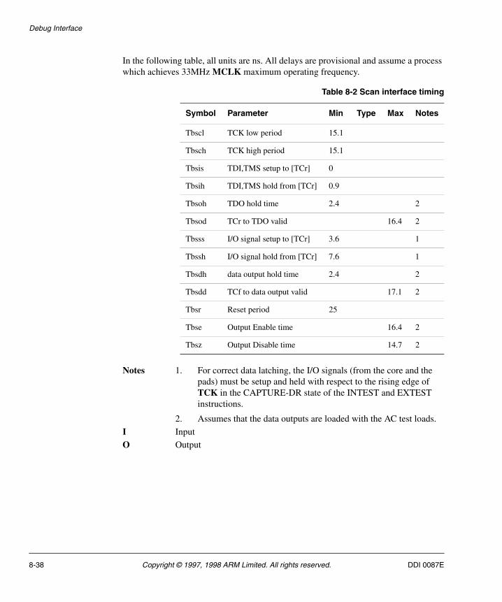
Debug Interface
In the following table, all units are ns. All delays are provisional and assume a process which achieves 33MHz MCLK maximum operating frequency.
Notes 1. For correct data latching, the I/O signals (from the core and the pads) must be setup and held with respect to the rising edge of TCK in the CAPTURE-DR state of the INTEST and EXTEST instructions.
2. Assumes that the data outputs are loaded with the AC test loads.
I Input
O Output
Table 8-2 Scan interface timing
Symbol Parameter Min Type Max Notes
Tbscl TCK low period 15.1
Tbsch TCK high period 15.1
Tbsis TDI,TMS setup to [TCr] 0
Tbsih TDI,TMS hold from [TCr] 0.9
Tbsoh TDO hold time 2.4 2
Tbsod TCr to TDO valid 16.4 2
Tbsss I/O signal setup to [TCr] 3.6 1
Tbssh I/O signal hold from [TCr] 7.6 1
Tbsdh data output hold time 2.4 2
Tbsdd TCf to data output valid 17.1 2
Tbsr Reset period 25
Tbse Output Enable time 16.4 2
Tbsz Output Disable time 14.7 2
8-38 Copyright © 1997, 1998 ARM Limited. All rights reserved. DDI 0087E
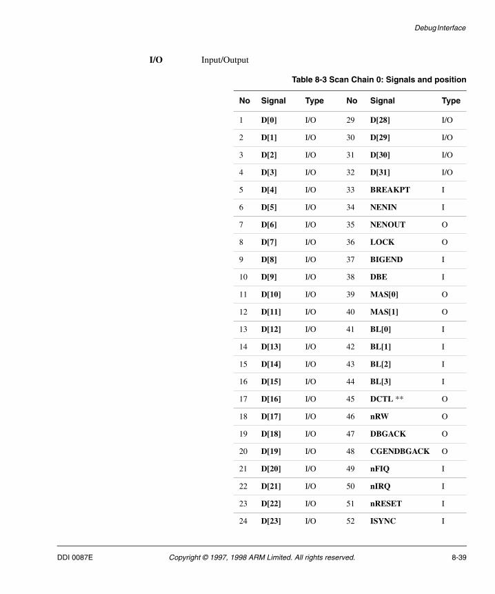
Debug Interface
I/O Input/Output
Table 8-3 Scan Chain 0: Signals and position
No Signal Type No Signal Type
1 D[0] I/O 29 D[28] I/O
2 D[1] I/O 30 D[29] I/O
3 D[2] I/O 31 D[30] I/O
4 D[3] I/O 32 D[31] I/O
5 D[4] I/O 33 BREAKPT I
6 D[5] I/O 34 NENIN I
7 D[6] I/O 35 NENOUT O
8 D[7] I/O 36 LOCK O
9 D[8] I/O 37 BIGEND I
10 D[9] I/O 38 DBE I
11 D[10] I/O 39 MAS[0] O
12 D[11] I/O 40 MAS[1] O
13 D[12] I/O 41 BL[0] I
14 D[13] I/O 42 BL[1] I
15 D[14] I/O 43 BL[2] I
16 D[15] I/O 44 BL[3] I
17 D[16] I/O 45 DCTL ** O
18 D[17] I/O 46 nRW O
19 D[18] I/O 47 DBGACK O
20 D[19] I/O 48 CGENDBGACK O
21 D[20] I/O 49 nFIQ I
22 D[21] I/O 50 nIRQ I
23 D[22] I/O 51 nRESET I
24 D[23] I/O 52 ISYNC I
DDI 0087E Copyright © 1997, 1998 ARM Limited. All rights reserved. 8-39

Debug Interface
25 D[24] I/O 53 DBGRQ I
26 D[25] I/O 54 ABORT I
27 D[26] I/O 55 CPA I
28 D[27] I/O 56 nOPC O
57 IFEN I 82 A[23] O
58 nCPI O 83 A[22] O
59 nMREQ O 84 A[21] O
60 SEQ O 85 A[20] O
61 nTRANS O 86 A[19] O
62 CPB I 87 A[18] O
63 nM[4] O 88 A[17] O
64 nM[3] O 89 A[16] O
65 nM[2] O 90 A[15] O
66 nM[1] O 91 A[14] O
67 nM[0] O 92 A[13] O
68 nEXEC O 93 A[12] O
69 ALE I 94 A[11] O
70 ABE I 95 A[10] O
71 APE I 96 A[9] O
72 TBIT O 97 A[8] O
73 nWAIT I 98 A[7] O
74 A[31] O 99 A[6] O
75 A[30] O 100 A[5] O
76 A[29] O 101 A[4] O
77 A[28] O 102 A[3] O
Table 8-3 Scan Chain 0: Signals and position (continued)
No Signal Type No Signal Type
8-40 Copyright © 1997, 1998 ARM Limited. All rights reserved. DDI 0087E
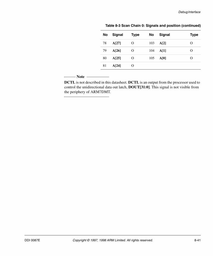
Debug Interface
Note DCTL is not described in this datasheet. DCTL is an output from the processor used to control the unidirectional data out latch, DOUT[31:0]. This signal is not visible from the periphery of ARM7DMT.
78 A[27] O 103 A[2] O
79 A[26] O 104 A[1] O
80 A[25] O 105 A[0] O
81 A[24] O
Table 8-3 Scan Chain 0: Signals and position (continued)
No Signal Type No Signal Type
DDI 0087E Copyright © 1997, 1998 ARM Limited. All rights reserved. 8-41

Debug Interface
8-42 Copyright © 1997, 1998 ARM Limited. All rights reserved. DDI 0087E
Chapter 9 EmbeddedICE Macrocell
This chapter describes the ARM720T EmbeddedICE module.
The ARM7DMT EmbeddedICE module, referred to simply as EmbeddedICE, provides integrated on-chip debug support for the ARM7DMT core.
• Overview on page 9-2
• The Watchpoint Registers on page 9-5
• Programming Breakpoints on page 9-10
• Programming Watchpoints on page 9-12
• The Debug Control Register on page 9-14
• Debug Status Register on page 9-16
• Coupling Breakpoints and Watchpoints on page 9-18
• Debug Communications Channel on page 9-20.
DDI 0087E Copyright © 1997, 1998 ARM Limited. All rights reserved. 9-1
EmbeddedICE Macrocell
9.1 Overview
In this chapter ARM7DMT refers to the ARM7TDMI core excluding the EmbeddedICE Macrocell. EmbeddedICE is programmed in a serial fashion using the ARM7DMT TAP controller. It consists of two real-time watchpoint units, together with a control and status register. One or both watchpoint units can be programmed to halt the execution of instructions by the ARM7DMT core via its BREAKPT signal.
Two independent registers, Debug Control and Debug Status, provide overall control of EmbeddedICE's operation. Figure 9-1 on page 9-3 shows the relationship between the core, EmbeddedICE and the TAP controller.
Execution is halted when a match occurs between the values programmed into EmbeddedICE and the values currently appearing on the address bus, data bus and various control signals. Any bit can be masked so that its value does not affect the comparison.
Note Only those signals that are pertinent to EmbeddedICE are shown.
In the ARM720T, the EmbeddedICE module is connected directly to the ARM7DMT Core and therefore functions on the virtual address of the processor after relocation by the task ID.
9-2 Copyright © 1997, 1998 ARM Limited. All rights reserved. DDI 0087E
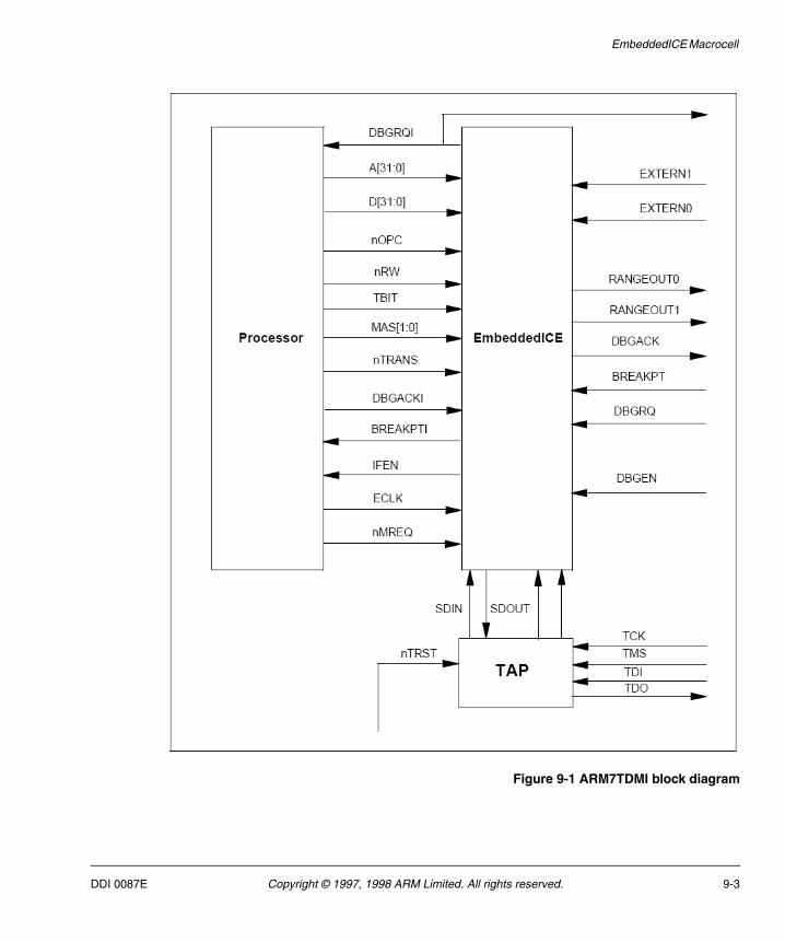
EmbeddedICE Macrocell
Figure 9-1 ARM7TDMI block diagram
DDI 0087E Copyright © 1997, 1998 ARM Limited. All rights reserved. 9-3
EmbeddedICE Macrocell
Either watchpoint unit can be configured to be a watchpoint (monitoring data accesses) or a breakpoint (monitoring instruction fetches). Watchpoints and breakpoints can be made to be data-dependent.
9.1.1 Disabling EmbeddedICE
EmbeddedICE may be disabled by wiring the DBGEN input LOW.
When DBGEN is LOW, BREAKPT and DBGRQ to the core are forced LOW, DBGACK from the ARM7DMT is also forced LOW and the IFEN input to the core is forced HIGH, enabling interrupts to be detected by ARM7DMT.
When DBGEN is LOW, EmbeddedICE is also put into a low-power mode.
9.1.2 EmbeddedICE timing
The EXTERN1 and EXTERN0 inputs are sampled by EmbeddedICE on the falling edge of ECLK. Sufficient set-up and hold time must therefore be allowed for these signals.
9-4 Copyright © 1997, 1998 ARM Limited. All rights reserved. DDI 0087E
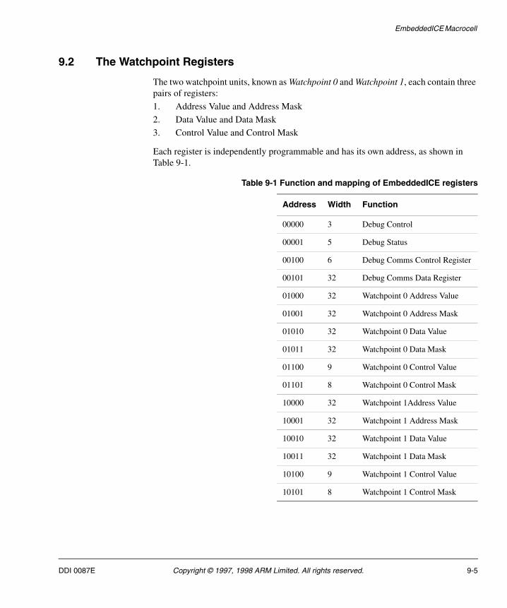
EmbeddedICE Macrocell
9.2 The Watchpoint Registers
The two watchpoint units, known as Watchpoint 0 and Watchpoint 1, each contain three pairs of registers:
1. Address Value and Address Mask
2. Data Value and Data Mask
3. Control Value and Control Mask
Each register is independently programmable and has its own address, as shown in Table 9-1.
Table 9-1 Function and mapping of EmbeddedICE registers
Address Width Function
00000 3 Debug Control
00001 5 Debug Status
00100 6 Debug Comms Control Register
00101 32 Debug Comms Data Register
01000 32 Watchpoint 0 Address Value
01001 32 Watchpoint 0 Address Mask
01010 32 Watchpoint 0 Data Value
01011 32 Watchpoint 0 Data Mask
01100 9 Watchpoint 0 Control Value
01101 8 Watchpoint 0 Control Mask
10000 32 Watchpoint 1Address Value
10001 32 Watchpoint 1 Address Mask
10010 32 Watchpoint 1 Data Value
10011 32 Watchpoint 1 Data Mask
10100 9 Watchpoint 1 Control Value
10101 8 Watchpoint 1 Control Mask
DDI 0087E Copyright © 1997, 1998 ARM Limited. All rights reserved. 9-5

EmbeddedICE Macrocell
9.2.1 Programming and reading watchpoint registers
A register is programmed by scanning data into the EmbeddedICE scan chain (scan chain 2). The scan chain consists of a 38-bit shift register comprising:
• a 32-bit data field
• a 5-bit address field
• a read/write bit
This is shown in Figure 9-2.
Figure 9-2 EmbeddedICE block diagram
The data to be written is scanned into the 32-bit data field, the address of the register into the 5-bit address field and a 1 into the read/write bit.
A register is read by scanning its address into the address field and scanning a 0 into the read/write bit. The 32-bit data field is ignored. The register addresses are shown in Table 9-1 on page 9-5.
9-6 Copyright © 1997, 1998 ARM Limited. All rights reserved. DDI 0087E
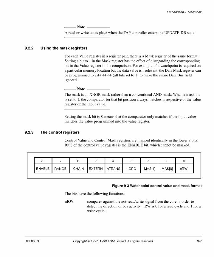
EmbeddedICE Macrocell
Note A read or write takes place when the TAP controller enters the UPDATE-DR state.
9.2.2 Using the mask registers
For each Value register in a register pair, there is a Mask register of the same format. Setting a bit to 1 in the Mask register has the effect of disregarding the corresponding bit in the Value register in the comparison. For example, if a watchpoint is required on a particular memory location but the data value is irrelevant, the Data Mask register can be programmed to 0xFFFFFFFF (all bits set to 1) to make the entire Data Bus field ignored.
Note The mask is an XNOR mask rather than a conventional AND mask. When a mask bit is set to 1, the comparator for that bit position always matches, irrespective of the value register or the input value.
Setting the mask bit to 0 means that the comparator only matches if the input value matches the value programmed into the value register.
9.2.3 The control registers
Control Value and Control Mask registers are mapped identically in the lower 8 bits. Bit 8 of the control value register is the ENABLE bit, which cannot be masked.
Figure 9-3 Watchpoint control value and mask format
The bits have the following functions:
nRW compares against the not-read/write signal from the core in order to detect the direction of bus activity. nRW is 0 for a read cycle and 1 for a write cycle.
DDI 0087E Copyright © 1997, 1998 ARM Limited. All rights reserved. 9-7

EmbeddedICE Macrocell
MAS[1:0] compares against the MAS[1:0] signal from the core in order to detect the size of bus activity. The encoding is shown in the following table.
nOPC detects whether the current cycle is an instruction fetch (nOPC = 0) or a data access (nOPC = 1).
nTRANS compares against the not-translate signal from the core in order to distinguish between User mode (nTRANS = 0) and non-User mode (nTRANS = 1) accesses.
EXTERN is an external input to EmbeddedICE which allows the watchpoint to be dependent upon an external condition. The EXTERN input for Watchpoint 0 is labelled EXTERN0 and the EXTERN input for Watchpoint 1 is labelled EXTERN1.
CHAIN can be connected to the chain output of another watchpoint in order to implement, for example, debugger requests of the form “breakpoint on address YYY only when in process XXX”.
In the ARM7DMT-EmbeddedICE, the CHAINOUT output of Watchpoint 1 is connected to the CHAIN input of Watchpoint 0. The CHAINOUT output is derived from a latch; the address/control field comparator drives the write enable for the latch and the input to the latch is the value of the data field comparator. The CHAINOUT latch is cleared when the Control Value register is written or when nTRST is LOW.
RANGE can be connected to the range output of another watchpoint register. In the ARM7DMT EmbeddedICE, the RANGEOUT output of Watchpoint 1 is connected to the RANGE input of Watchpoint 0. This allows the two watchpoints to be coupled for detecting conditions that occur simultaneously, for example, in range-checking.
Table 9-2 MAS[1:0] signal encoding
bit 1 bit 0 Data size
0 0 byte
0 1 halfword
1 0 word
1 1 (reserved)
9-8 Copyright © 1997, 1998 ARM Limited. All rights reserved. DDI 0087E
EmbeddedICE Macrocell
ENABLE only exists in the value register and it cannot be masked. If a watchpoint match occurs, the BREAKPT signal is asserted only when the ENABLE bit is set.
For each of the bits [8:0] in the Control Value register, there is a corresponding bit in the Control Mask register. This removes the dependency on particular signals.
DDI 0087E Copyright © 1997, 1998 ARM Limited. All rights reserved. 9-9

EmbeddedICE Macrocell
9.3 Programming Breakpoints
Breakpoints can be classified as hardware breakpoints or software breakpoints.
Hardware These typically monitor the address value and can be set in any code, even in code that is in ROM or code that is self-modifying.
Software These monitor a particular bit pattern being fetched from any address. One EmbeddedICE watchpoint can thus be used to support any number of software breakpoints. Software breakpoints can normally only be set in RAM because an instruction has to be replaced by the special bit pattern chosen to cause a software breakpoint.
9.3.1 Hardware breakpoints
To make a watchpoint unit cause hardware breakpoints (that is, on instruction fetches):
1. To make a watchpoint unit cause hardware breakpoints (that is, on instruction fetches):
2. Program the breakpoint bits as follows:
ARM state set bits [1:0] of the Address Mask register to 1.
THUMB state set bit 0 of the Address Mask to 1.
In both cases, the remaining bits are set to 0.
3. Program the Data Value register only if you require a data-dependent breakpoint: that is, only if the actual instruction code fetched must be matched as well as the address. If the data value is not required, program the Data Mask register to 0xFFFFFFFF (all bits to1), otherwise program it to 0x00000000.
4. Program the Control Value register with nOPC = 0.
5. Program the Control Mask register with nOPC =0, all other bits to 1.
6. If you need to make the distinction between user and non-user mode instruction fetches, program the nTRANS Value and Mask bits as above.
7. If required, program the EXTERN, RANGE and CHAIN bits in the same way.
9.3.2 Software breakpoints
To make a watchpoint unit cause software breakpoints (that is, on instruction fetches of a particular bit pattern):
1. Program its Address Mask register to 0xFFFFFFFF (all bits set to 1) so that the address is disregarded.
9-10 Copyright © 1997, 1998 ARM Limited. All rights reserved. DDI 0087E
EmbeddedICE Macrocell
2. Program its Address Mask register to 0xFFFFFFFF (all bits set to 1) so that the address is disregarded.
For a THUMB software breakpoint, the 16-bit pattern must be repeated in both halves of the Data Value register. For example, if the bit pattern is 0xDFFF, then 0xDFFFDFFF must be programmed. When a 16-bit instruction is fetched, EmbeddedICE only compares the valid half of the data bus against the contents of the Data Value register. In this way, a single Watchpoint register can be used to catch software breakpoints on both the upper and lower halves of the data bus.
3. Program the Data Mask register to 0x00000000.
4. Program the Control Value register with nOPC = 0.
5. Program the Control Mask register with nOPC = 0, all other bits to 1.
6. If you wish to make the distinction between user and non-user mode instruction fetches, program the nTRANS bit in the Control Value and Control Mask registers accordingly.
7. If required, program the EXTERN, RANGE and CHAIN bits in the same way.
Note The address value register need not be programmed.
Setting the breakpoint
To set the software breakpoint:
1. Read the instruction at the desired address and store it.
2. Write the special bit pattern representing a software breakpoint at the address.
Clearing the breakpoint
To clear the software breakpoint, restore the instruction to the address.
DDI 0087E Copyright © 1997, 1998 ARM Limited. All rights reserved. 9-11
EmbeddedICE Macrocell
9.4 Programming Watchpoints
These are just examples of how to program the watchpoint register to generate breakpoints and watchpoints; many other ways of programming the registers are possible. For instance, simple range breakpoints can be provided by setting one or more of the address mask bits.
To make a watchpoint unit cause watchpoints (ie on data accesses):
1. Program its Address Value register with the address of the data access to be watchpointed.
2. Program the Address Mask register to 0x00000000.
3. Program the Data Value register only if you require a data-dependent watchpoint; that is, only if the actual data value read or written must be matched as well as the address. If the data value is irrelevant, program the Data Mask register to 0xFFFFFFFF (all bits set to 1) otherwise program it to 0x00000000.
4. Program the Control Value register with:
nOPC = 1
nRW = 0 for a read
nRW = 1 for a write
MAS[1:0] with the value corresponding to the appropriate data size.
5. Program the Control Mask register with:
nOPC = 0
nRW = 0
MAS[1:0] = 0
all other bits to 1
Note that nRW or MAS[1:0] may be set to 1 if both reads and writes or data size accesses are to be watchpointed respectively.
6. If you wish to make the distinction between user and non-user mode data accesses, program the nTRANS bit in the Control Value and Control Mask registers accordingly.
7. If required, program the EXTERN, RANGE and CHAIN bits in the same way.
9.4.1 Programming restriction
The EmbeddedICE watchpoint units should only be programmed when the clock to the core is stopped. This can be achieved by putting the core into the debug state.
9-12 Copyright © 1997, 1998 ARM Limited. All rights reserved. DDI 0087E
EmbeddedICE Macrocell
The reason for this restriction is that if the core continues to run at ECLK rates when EmbeddedICE is being programmed at TCK rates, it is possible for the BREAKPT signal to be asserted asynchronously to the core.
This restriction does not apply if MCLK and TCK are driven from the same clock, or if it is known that the breakpoint or watchpoint condition can only occur some time after EmbeddedICE has been programmed.
Note This restriction does not apply to the Debug Control or Status Registers.
DDI 0087E Copyright © 1997, 1998 ARM Limited. All rights reserved. 9-13
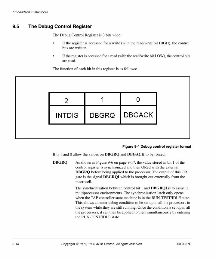
EmbeddedICE Macrocell
9.5 The Debug Control Register
The Debug Control Register is 3 bits wide.
• If the register is accessed for a write (with the read/write bit HIGH), the control bits are written.
• If the register is accessed for a read (with the read/write bit LOW), the control bits are read.
The function of each bit in this register is as follows:
Figure 9-4 Debug control register format
Bits 1 and 0 allow the values on DBGRQ and DBGACK to be forced.
DBGRQ As shown in Figure 9-6 on page 9-17, the value stored in bit 1 of the control register is synchronized and then ORed with the external DBGRQ before being applied to the processor. The output of this OR gate is the signal DBGRQI which is brought out externally from the macrocell.
The synchronization between control bit 1 and DBGRQI is to assist in multiprocessor environments. The synchronisation latch only opens when the TAP controller state machine is in the RUN-TEST/IDLE state. This allows an enter debug condition to be set up in all the processors in the system while they are still running. Once the condition is set up in all the processors, it can then be applied to them simultaneously by entering the RUN-TEST/IDLE state.
9-14 Copyright © 1997, 1998 ARM Limited. All rights reserved. DDI 0087E
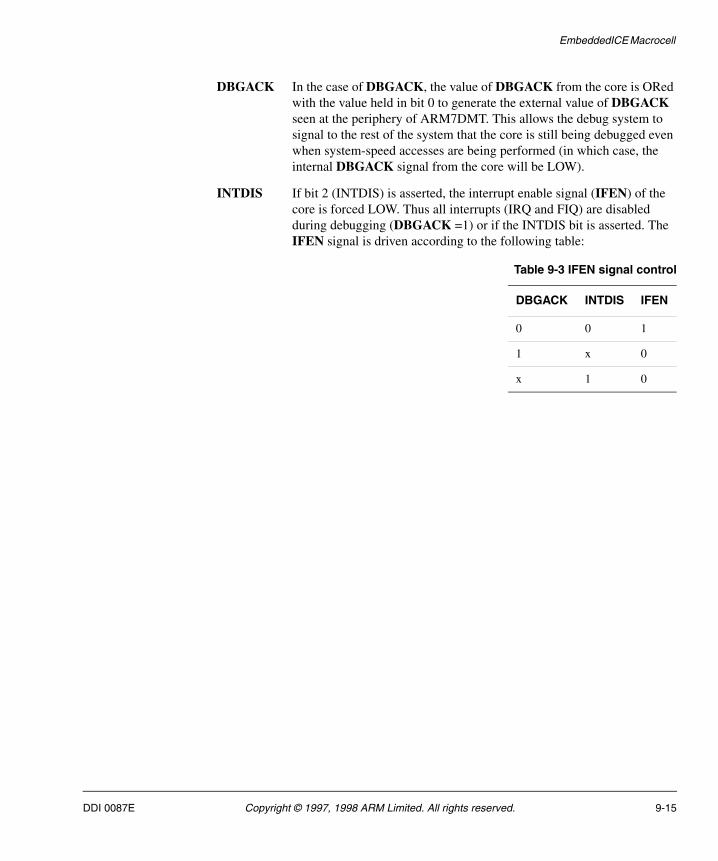
EmbeddedICE Macrocell
DBGACK In the case of DBGACK, the value of DBGACK from the core is ORed with the value held in bit 0 to generate the external value of DBGACK seen at the periphery of ARM7DMT. This allows the debug system to signal to the rest of the system that the core is still being debugged even when system-speed accesses are being performed (in which case, the internal DBGACK signal from the core will be LOW).
INTDIS If bit 2 (INTDIS) is asserted, the interrupt enable signal (IFEN) of the core is forced LOW. Thus all interrupts (IRQ and FIQ) are disabled during debugging (DBGACK =1) or if the INTDIS bit is asserted. The IFEN signal is driven according to the following table:
Table 9-3 IFEN signal control
DBGACK INTDIS IFEN
0 0 1
1 x 0
x 1 0
DDI 0087E Copyright © 1997, 1998 ARM Limited. All rights reserved. 9-15
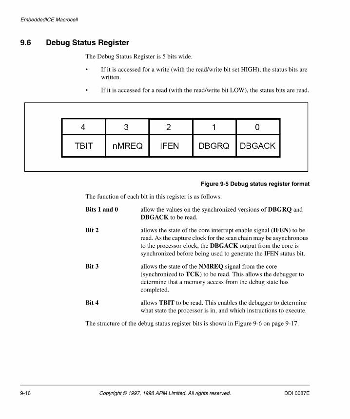
EmbeddedICE Macrocell
9.6 Debug Status Register
The Debug Status Register is 5 bits wide.
• If it is accessed for a write (with the read/write bit set HIGH), the status bits are written.
• If it is accessed for a read (with the read/write bit LOW), the status bits are read.
Figure 9-5 Debug status register format
The function of each bit in this register is as follows:
Bits 1 and 0 allow the values on the synchronized versions of DBGRQ and DBGACK to be read.
Bit 2 allows the state of the core interrupt enable signal (IFEN) to be read. As the capture clock for the scan chain may be asynchronous to the processor clock, the DBGACK output from the core is synchronized before being used to generate the IFEN status bit.
Bit 3 allows the state of the NMREQ signal from the core (synchronized to TCK) to be read. This allows the debugger to determine that a memory access from the debug state has completed.
Bit 4 allows TBIT to be read. This enables the debugger to determine what state the processor is in, and which instructions to execute.
The structure of the debug status register bits is shown in Figure 9-6 on page 9-17.
9-16 Copyright © 1997, 1998 ARM Limited. All rights reserved. DDI 0087E
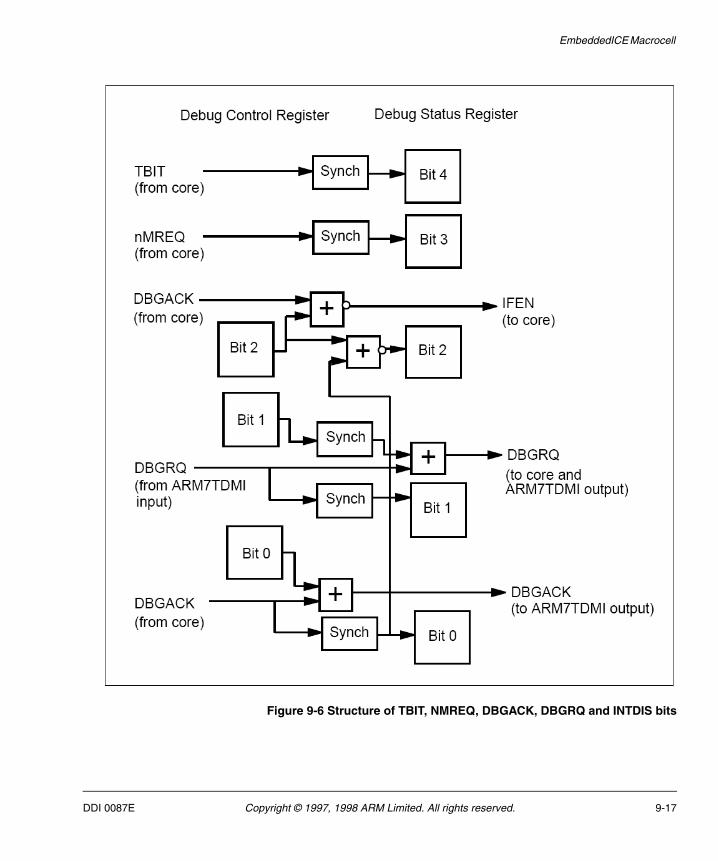
EmbeddedICE Macrocell
Figure 9-6 Structure of TBIT, NMREQ, DBGACK, DBGRQ and INTDIS bits
DDI 0087E Copyright © 1997, 1998 ARM Limited. All rights reserved. 9-17
EmbeddedICE Macrocell
9.7 Coupling Breakpoints and Watchpoints
Watchpoint units 1 and 0 can be coupled together via the CHAIN and RANGE inputs.
CHAIN enables watchpoint 0 to be triggered only if watchpoint 1 has previously matched.
RANGE enables simple range checking to be performed by combining the outputs of both watchpoints.
9.7.1 Example
Let
Av[31:0] be the value in the Address Value Register.
Am[31:0] be the value in the Address Mask Register.
A[31:0] be the Address Bus from the ARM7DMT.
Dv[31:0] be the value in the Data Value Register.
Dm[31:0] be the value in the Data Mask Register.
D[31:0] be the Data Bus from the ARM7DMT.
Cv[8:0] be the value in the Control Value Register.
Cm[7:0] be the value in the Control Mask Register.
C[9:0] be the combined Control Bus from the ARM7DMT, other watchpoint registers and the EXTERN signal.
CHAINOUT signal
The CHAINOUT signal is then derived as follows:
WHEN (({Av[31:0],Cv[4:0]} XNOR {A[31:0],C[4:0]}) OR{Am[31:0],Cm[4:0]} == 0x1FFFFFFFFF)CHAINOUT = ((({Dv[31:0],Cv[7:5]} XNOR {D[31:0],C[7:5]}) OR{Dm[31:0],Cm[7:5]}) == 0x7FFFFFFFF)
The CHAINOUT output of watchpoint register 1 provides the CHAIN input to Watchpoint 0. This allows for quite complicated configurations of breakpoints and watchpoints.
For example, consider the request by a debugger to breakpoint on the instruction at location YYY when running process XXX in a multiprocess system.
9-18 Copyright © 1997, 1998 ARM Limited. All rights reserved. DDI 0087E
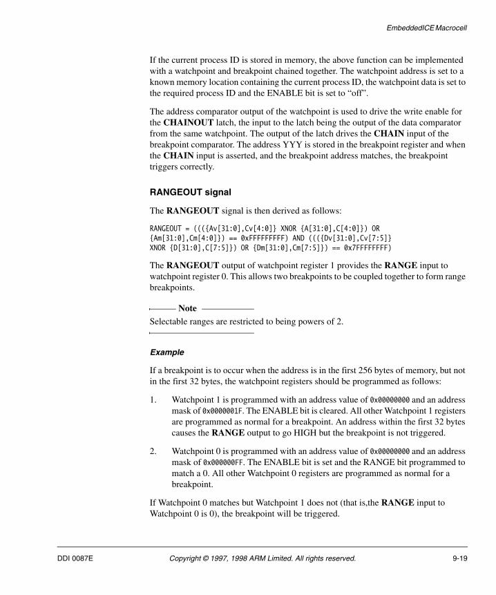
EmbeddedICE Macrocell
If the current process ID is stored in memory, the above function can be implemented with a watchpoint and breakpoint chained together. The watchpoint address is set to a known memory location containing the current process ID, the watchpoint data is set to the required process ID and the ENABLE bit is set to “off”.
The address comparator output of the watchpoint is used to drive the write enable for the CHAINOUT latch, the input to the latch being the output of the data comparator from the same watchpoint. The output of the latch drives the CHAIN input of the breakpoint comparator. The address YYY is stored in the breakpoint register and when the CHAIN input is asserted, and the breakpoint address matches, the breakpoint triggers correctly.
RANGEOUT signal
The RANGEOUT signal is then derived as follows:
RANGEOUT = ((({Av[31:0],Cv[4:0]} XNOR {A[31:0],C[4:0]}) OR{Am[31:0],Cm[4:0]}) == 0xFFFFFFFFF) AND ((({Dv[31:0],Cv[7:5]}XNOR {D[31:0],C[7:5]}) OR {Dm[31:0],Cm[7:5]}) == 0x7FFFFFFFF)
The RANGEOUT output of watchpoint register 1 provides the RANGE input to watchpoint register 0. This allows two breakpoints to be coupled together to form range breakpoints.
Note Selectable ranges are restricted to being powers of 2.
Example
If a breakpoint is to occur when the address is in the first 256 bytes of memory, but not in the first 32 bytes, the watchpoint registers should be programmed as follows:
1. Watchpoint 1 is programmed with an address value of 0x00000000 and an address mask of 0x0000001F. The ENABLE bit is cleared. All other Watchpoint 1 registers are programmed as normal for a breakpoint. An address within the first 32 bytes causes the RANGE output to go HIGH but the breakpoint is not triggered.
2. Watchpoint 0 is programmed with an address value of 0x00000000 and an address mask of 0x000000FF. The ENABLE bit is set and the RANGE bit programmed to match a 0. All other Watchpoint 0 registers are programmed as normal for a breakpoint.
If Watchpoint 0 matches but Watchpoint 1 does not (that is,the RANGE input to Watchpoint 0 is 0), the breakpoint will be triggered.
DDI 0087E Copyright © 1997, 1998 ARM Limited. All rights reserved. 9-19
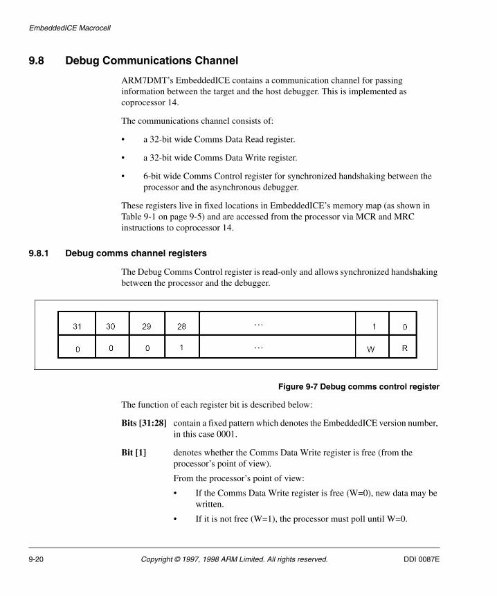
EmbeddedICE Macrocell
9.8 Debug Communications Channel
ARM7DMT’s EmbeddedICE contains a communication channel for passing information between the target and the host debugger. This is implemented as coprocessor 14.
The communications channel consists of:
• a 32-bit wide Comms Data Read register.
• a 32-bit wide Comms Data Write register.
• 6-bit wide Comms Control register for synchronized handshaking between the processor and the asynchronous debugger.
These registers live in fixed locations in EmbeddedICE’s memory map (as shown in Table 9-1 on page 9-5) and are accessed from the processor via MCR and MRC instructions to coprocessor 14.
9.8.1 Debug comms channel registers
The Debug Comms Control register is read-only and allows synchronized handshaking between the processor and the debugger.
Figure 9-7 Debug comms control register
The function of each register bit is described below:
Bits [31:28] contain a fixed pattern which denotes the EmbeddedICE version number, in this case 0001.
Bit [1] denotes whether the Comms Data Write register is free (from the processor’s point of view).
From the processor’s point of view:
• If the Comms Data Write register is free (W=0), new data may be written.
• If it is not free (W=1), the processor must poll until W=0.
9-20 Copyright © 1997, 1998 ARM Limited. All rights reserved. DDI 0087E
EmbeddedICE Macrocell
From the debugger’s point of view, if W=1, new data has been written which may then be scanned out.
Bit [0] denotes whether there is some new data in the Comms Data Read register.
From the processor’s point of view:
• If R=1, there is some new data which may be read via an MRC instruction.
From the debugger’s point of view:
• If R=0, the Comms Data Read register is free and new data may be placed there through the scan chain.
• If R=1, this denotes that data previously placed there through the scan chain has not been collected by the processor and so the debugger must wait.
From the debugger’s point of view, the registers are accessed via the scan chain in the usual way. From the processors point of view, these registers are accessed via coprocessor register transfer instructions.
Instructions
The following instructions should be used.
This instruction returns the Debug Comms Control register into Rd.
MRC CP14, 0, Rd, C0, C0
This instruction writes the value in Rn to the Comms Data Write register.
MCR CP14, 0, Rn, C1, C0
This instruction returns the Debug Data Read register into Rd.
MRC CP14, 0, Rd, C1, C0
Note As the THUMB instruction set does not contain coprocessor instructions, it is recommended that these are accessed via SWI instructions when in THUMB state.
DDI 0087E Copyright © 1997, 1998 ARM Limited. All rights reserved. 9-21
EmbeddedICE Macrocell
9.8.2 Communications via the comms channel
Communication between the debugger and the processor occurs as follows.
1. When the processor wishes to send a message to EmbeddedICE, it first checks that the Comms Data Write register is free for use.
2. This is done by reading the Debug Comms Control register to check that the W bit is clear:
• If it is clear, the Comms Data Write register is empty and a message is written by a register transfer to the coprocessor. The action of this data transfer automatically sets the W bit.
• If it is set, this implies that previously-written data has not been picked up by the debugger and the processor must poll until the W bit is clear.
3. Because the data transfer occurs from the processor to the Comms Data Write register, the W bit is set in the Debug Comms Control register.
4. When the debugger polls this register, it sees a synchronized version of both the R and W bit.
• When the debugger sees that the W bit is set, it can read the Comms Data Write register and scan the data out.
• The action of reading this data register clears the W bit of the Debug Comms Control register. At this point, the communications process may begin again.
9.8.3 Message transfer
Message transfer from the debugger to the processor is carried out in a similar fashion:
1. The debugger polls the R bit of the Debug Comms Control register:
• If the R bit is low, the Data Read register is free and so data can be placed there for the processor to read.
• If the R bit is set, previously deposited data has not yet been collected and so the debugger must wait.
2. When the Comms Data Read register is free, data is written there via the scan chain. The action of this write sets the R bit in the Debug Comms Control register.
3. When the processor polls this register, it sees an MCLK synchronized version.
• If the R bit is set, this denotes that there is data waiting to be collected, and this can be read via a CPRT load. The action of this load clears the R bit in the Debug Comms Control register.
9-22 Copyright © 1997, 1998 ARM Limited. All rights reserved. DDI 0087E
EmbeddedICE Macrocell
• If the R bit is clear, this denotes that the data has been taken and the process may now be repeated.
DDI 0087E Copyright © 1997, 1998 ARM Limited. All rights reserved. 9-23
EmbeddedICE Macrocell
9-24 Copyright © 1997, 1998 ARM Limited. All rights reserved. DDI 0087E
Chapter 10 Bus Clocking
This chapter describes the bus interface clocking.
• Introduction on page 10-2
• Fastbus Extension on page 10-3
• Standard Mode on page 10-5.
DDI 0087E Copyright © 1997, 1998 ARM Limited. All rights reserved. 10-1
Bus Clocking
10.1 Introduction
The ARM720T bus interface can be operated using either:
• the standard mode of operation
• the new fastbus extension
As the ARM720T is a fully static design, the clock can be stopped indefinitely in either mode of operation. Care should be taken to ensure that the memory system does not dissipate power in the state in which it is stopped.
10.1.1 Standard mode
For designs using low-cost, low-speed memory, and if operation of the core at a faster speed is required, it is recommended that you use standard mode.
This mode consists of:
• two clocks, FCLK and BCLK• synchronous or fully asynchronous operation
10.1.2 Fastbus extension
For new designs, you can operate the device using the fastbus extension. In fastbus mode, the device is clocked off a single clock, and the bus is operated at the same frequency as the core. This allows the bus interface to be clocked faster than if the device is operated in standard mode. It is recommended that you use this mode of operation in systems with high-speed memory and a single clock.
This mode consists of:
• single device clock
• increased maximum BCLK frequency
10-2 Copyright © 1997, 1998 ARM Limited. All rights reserved. DDI 0087E
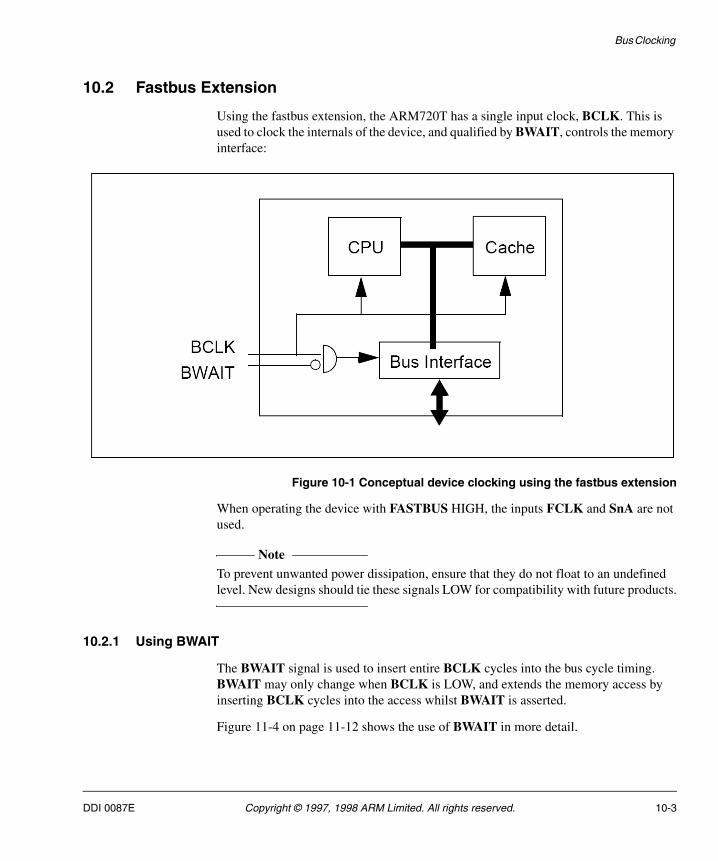
Bus Clocking
10.2 Fastbus Extension
Using the fastbus extension, the ARM720T has a single input clock, BCLK. This is used to clock the internals of the device, and qualified by BWAIT, controls the memory interface:
Figure 10-1 Conceptual device clocking using the fastbus extension
When operating the device with FASTBUS HIGH, the inputs FCLK and SnA are not used.
Note To prevent unwanted power dissipation, ensure that they do not float to an undefined level. New designs should tie these signals LOW for compatibility with future products.
10.2.1 Using BWAIT
The BWAIT signal is used to insert entire BCLK cycles into the bus cycle timing. BWAIT may only change when BCLK is LOW, and extends the memory access by inserting BCLK cycles into the access whilst BWAIT is asserted.
Figure 11-4 on page 11-12 shows the use of BWAIT in more detail.
DDI 0087E Copyright © 1997, 1998 ARM Limited. All rights reserved. 10-3
Bus Clocking
Memory cycles
It is preferable to use BWAIT to extend memory cycles, rather than stretching BCLK externally to the device because it is possible for the core to be accessing the Cache while bus activity is occurring. This allows the maximum performance, as the Core can to continue execution in parallel with the memory bus activity. All BCLK cycles are available to the CPU and Cache, regardless of the state of BWAIT.
In some circumstances, it may be desirable to stretch BCLK phases in order to match memory timing which is not an integer multiple of BCLK. There are certain cases where this results in a higher performance than using BWAIT to extend the access by an integer number of cycles.
CPU and Cache operation
CPU and Cache operation can only continue in parallel with buffered writes to the external bus. For all read accesses, the CPU is stalled until the bus activity has completed. So, if read accesses can be achieved faster by stretching BCLK rather than using BWAIT, this results in improved performance. An example of where this may be useful would be to interface to a ROM which has a cycle time of 2.5 times the BCLK period.
10-4 Copyright © 1997, 1998 ARM Limited. All rights reserved. DDI 0087E
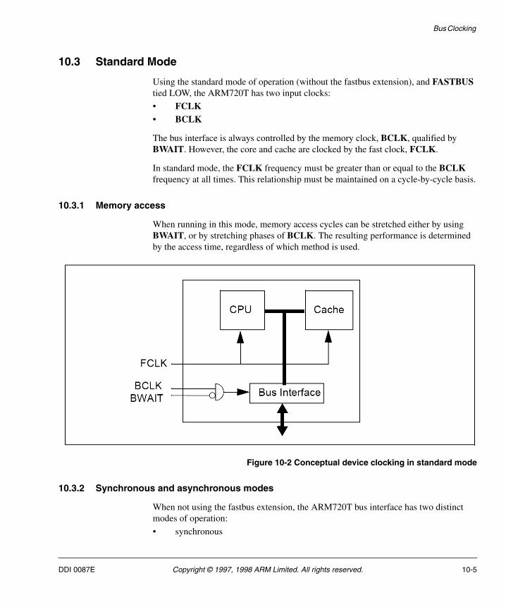
Bus Clocking
10.3 Standard Mode
Using the standard mode of operation (without the fastbus extension), and FASTBUS tied LOW, the ARM720T has two input clocks:
• FCLK• BCLK
The bus interface is always controlled by the memory clock, BCLK, qualified by BWAIT. However, the core and cache are clocked by the fast clock, FCLK.
In standard mode, the FCLK frequency must be greater than or equal to the BCLK frequency at all times. This relationship must be maintained on a cycle-by-cycle basis.
10.3.1 Memory access
When running in this mode, memory access cycles can be stretched either by using BWAIT, or by stretching phases of BCLK. The resulting performance is determined by the access time, regardless of which method is used.
Figure 10-2 Conceptual device clocking in standard mode
10.3.2 Synchronous and asynchronous modes
When not using the fastbus extension, the ARM720T bus interface has two distinct modes of operation:
• synchronous
DDI 0087E Copyright © 1997, 1998 ARM Limited. All rights reserved. 10-5
Bus Clocking
• asynchronous
These are selected by tying SnA either HIGH or LOW.
FCLK and BCLK
The two modes differ in the relationship between FCLK and BCLK:
• In asynchronous mode (SnA LOW), the clocks may be completely asynchronous and of unrelated frequency.
• In synchronous mode (SnA HIGH), BCLK may only make transitions before the falling edge of FCLK.
In systems where a satisfactory relationship exists between FCLK and BCLK, synchronization penalties can be avoided by selecting the synchronous mode of operation.
Asynchronous mode
In this mode, FCLK and BCLK may be completely asynchronous. You should select this mode by tying SnA LOW when the two clocks are of unrelated frequency.
There is a synchronization penalty whenever the internal core clock switches between the two input clocks. This penalty is symmetrical, and varies between zero and a whole period of the clock to which the core is resynchronizing:
• when changing from FCLK to BCLK, the average resynchronisation penalty is half an BCLK period
• when changing from BCLK to FCLK, the average resynchronisation penalty is half an FCLK period.
Synchronous mode
You select this mode by tying SnA HIGH. In this mode, here is a tightly defined relationship between FCLK and BCLK, in that BCLK may only make transitions on the falling edge of FCLK. Some jitter between the two clocks is permitted, but BCLK must meet the setup and hold requirements relative to FCLK.
10-6 Copyright © 1997, 1998 ARM Limited. All rights reserved. DDI 0087E
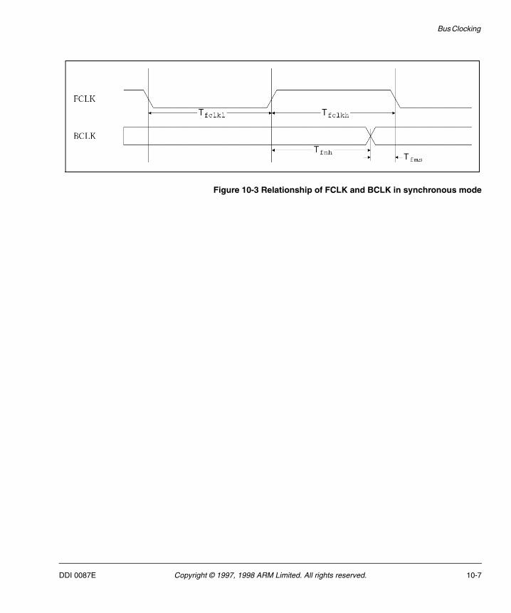
Bus Clocking
Figure 10-3 Relationship of FCLK and BCLK in synchronous mode
DDI 0087E Copyright © 1997, 1998 ARM Limited. All rights reserved. 10-7

Bus Clocking
10-8 Copyright © 1997, 1998 ARM Limited. All rights reserved. DDI 0087E
Chapter 11 AMBA Interface
This chapter describes the operation of the AMBA bus interface.
In normal operation, the ARM720T is an ASB (Advanced System Bus) bus master. As a bus master it performs a subset of the possible ASB cycle types.
The ASB is further described in the AMBA Specification, ARM IHI 0001.
• ASB Bus Interface Signals on page 11-2
• Cycle Types on page 11-3
• Addressing Signals on page 11-7
• Memory Request Signals on page 11-8
• Data Signal Timing on page 11-9
• Slave Response Signals on page 11-10
• Maximum Sequential Length on page 11-13
• Read-Lock-Write on page 11-14
• Big-Endian / Little-Endian Operation on page 11-15
• Multi-master Operation on page 11-18
• Bus Master Handover on page 11-20
• Default Bus Master on page 11-23.
DDI 0087E Copyright © 1997, 1998 ARM Limited. All rights reserved. 11-1
AMBA Interface
11.1 ASB Bus Interface Signals
The signals in the ASB interface can be grouped into four categories:
Addressing BA[31:0]
BWRITE
BSIZE [1:0]
BLOK
BPROT
Memory request BTRAN[1:0]
Data sampled BD[31:0]
Slave response BERROR
BWAIT
BLAST
System Arbiter
In addition to these signals, there are also three controls communicating with control logic in the system:
AGNT selects the ARM as a bus master
AREQ indicates that the ARM720T requires bus mastership
DSELARM selects the ARM as a bus slave
11-2 Copyright © 1997, 1998 ARM Limited. All rights reserved. DDI 0087E
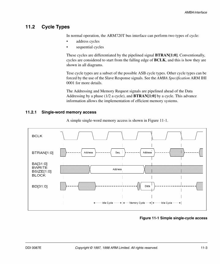
AMBA Interface
11.2 Cycle Types
In normal operation, the ARM720T bus interface can perform two types of cycle:
• address cycles
• sequential cycles
These cycles are differentiated by the pipelined signal BTRAN[1:0]. Conventionally, cycles are considered to start from the falling edge of BCLK, and this is how they are shown in all diagrams.
Tese cycle types are a subset of the possible ASB cycle types. Other cycle types can be forced by the use of the Slave Response signals. See the AMBA Specification ARM IHI 0001 for more details.
The Addressing and Memory Request signals are pipelined ahead of the Data Addressing by a phase (1/2 a cycle), and BTRAN[1:0] by a cycle. This advance information allows the implementation of efficient memory systems.
11.2.1 Single-word memory access
A simple single-word memory access is shown in Figure 11-1.
Figure 11-1 Simple single-cycle access
DDI 0087E Copyright © 1997, 1998 ARM Limited. All rights reserved. 11-3
AMBA Interface
The access starts with the address being broadcast. This can be used for decoding, but the access is not committed until BTRAN[1:0] (Bus Transaction Type) signals a sequential cycle in the following HIGH phase of BCLK. This indicates that the next cycle is a memory access cycle.
In this example, BTRAN[1:0] returns to Address after a single cycle, indicating that there will be a single memory access cycle, followed by an address cycle. The data is transferred on the falling edge of BCLK at the end of the sequential cycle.
Therefore, a memory access consists of:
• an address cycle, with a valid address
• a memory cycle with the same address
The initial address cycle allows the memory controller more time to decode the address. See Table 11-1 on page 11-8 for the encoding of BTRAN[1:0].
11.2.2 Sequential accesses
ARM720T can perform sequential bursts of accesses. These consist of:
• an address cycle and a sequential cycle, as shown previously
• further sequential cycles to:
— incrementing word addresses (that is, a, a+4, a+8 etc.), or
— halfword addresses (that is, a, a+2, a+4 etc.)
See Figure 11-2 on page 11-5. After the initial address cycle, the address is pipelined by 1/2 a bus cycle from the data.
Note BTRAN[1:0] is pipelined by a bus cycle from the data. If BWAIT is being used to stretch cycles, BTRAN[1:0] no longer refers to the next BCLK cycle, but rather to the next bus cycle. See BWAIT on page 11-10.
11-4 Copyright © 1997, 1998 ARM Limited. All rights reserved. DDI 0087E
AMBA Interface
Figure 11-2 Simple sequential access
Sequential bursts can occur on word or halfword accesses, and are always in the same direction, that is, Read (BWRITE LOW) or Write (BWRITE HIGH).
A memory controller should always qualify the use of the address with BTRAN[1:0]. There are certain circumstances in which a new address can be broadcast on the address bus, but BTRAN[1:0] does not signal a sequential access. This only happens when an internal (Protection Unit generated) abort occurs.
11.2.3 Bus accesses
The minimum interval between bus accesses can occur after a buffered write. In this case, there may only be a single address cycle between two memory cycles to non-sequential addresses. This means that the address for the second access is broadcast on BA[31:0] during the HIGH phase of the final memory cycle of the buffered write.
See Figure 11-3 on page 11-6 for more information.
DDI 0087E Copyright © 1997, 1998 ARM Limited. All rights reserved. 11-5
AMBA Interface
Figure 11-3 Minimum interval between bus accesses
This is the closest case of back-to-back cycles on the bus, and the memory controller should be designed to handle this case. In high-speed systems one solution is to use BWAIT to increase the decode and access time available for the second access.
Note Memory and peripheral strobes should not be direct decodes of the address bus. This could result in their changing during the last cycle of a write burst.
11-6 Copyright © 1997, 1998 ARM Limited. All rights reserved. DDI 0087E
AMBA Interface
11.3 Addressing Signals
Memory accesses may be read or write, and are differentiated by the signal BWRITE.
BWRITE may not change during a sequential access, so if a read from address A is followed immediately by a write to address (A+4), the write to address (A+4) is performed on the bus as a non-sequential access.
In the same way, any memory access may be a word, a half-word or a byte. These are differentiated by the signal BSIZE[1:0]. Again, BSIZE[1:0] may not change during sequential accesses. It is not possible to perform sequential byte accesses.
In order to reduce system power consumption, the addressing signals are left with their current values at the end of an access, until the next access occurs.
After a buffered write, there may be only a single address cycle between the two memory cycles. In this case, the next non-sequential address is broadcast in the last cycle of the previous access. This is the worst case for address decoding, as shown in Figure 11-3 on page 11-6.
DDI 0087E Copyright © 1997, 1998 ARM Limited. All rights reserved. 11-7
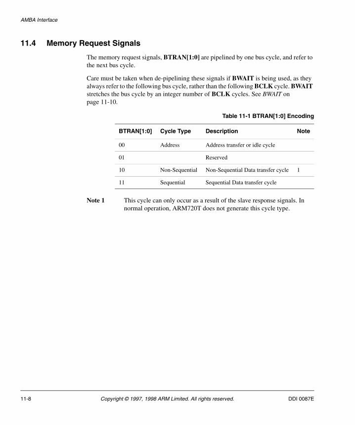
AMBA Interface
11.4 Memory Request Signals
The memory request signals, BTRAN[1:0] are pipelined by one bus cycle, and refer to the next bus cycle.
Care must be taken when de-pipelining these signals if BWAIT is being used, as they always refer to the following bus cycle, rather than the following BCLK cycle. BWAIT stretches the bus cycle by an integer number of BCLK cycles. See BWAIT on page 11-10.
Note 1 This cycle can only occur as a result of the slave response signals. In normal operation, ARM720T does not generate this cycle type.
Table 11-1 BTRAN[1:0] Encoding
BTRAN[1:0] Cycle Type Description Note
00 Address Address transfer or idle cycle
01 Reserved
10 Non-Sequential Non-Sequential Data transfer cycle 1
11 Sequential Sequential Data transfer cycle
11-8 Copyright © 1997, 1998 ARM Limited. All rights reserved. DDI 0087E
AMBA Interface
11.5 Data Signal Timing
During a read access, the data is sampled on the falling edge of BCLK at the end of the sequential cycle. During a write access, the data on BD[31:0] is timed off the falling edge of BCLK at the start of the memory cycle. If BWAIT is being used to stretch this cycle, the data is valid from the falling edge of BCLK at the end of the previous cycle, when BWAIT was HIGH. See BWAIT on page 11-10.
Note In a low-power system, you must ensure that the databus is not allowed to float to an undefined level. This causes power to be dissipated in the inputs of devices connected to the bus. This is particularly important when a system is put into a low-power sleep mode. It is recommended that one set of databus drivers in the system are left enabled during sleep to hold the bus at a defined level.
DDI 0087E Copyright © 1997, 1998 ARM Limited. All rights reserved. 11-9
AMBA Interface
11.6 Slave Response Signals
11.6.1 BERROR
The BERROR signal is sampled on the risingedgeof BCLK during a sequential cycle, on both read and write accesses. The effect of BERROR on the operation of the ARM720T is discussed in Exceptions on page 3-14.
BERROR can be flagged on any sequential cycle; however, it is ignored on buffered writes, which cannot be aborted.
Linefetches
The effect of BERROR during linefetches is slightly different to that during other access.During a linefetch the ARM720T fetches four words of data, regardless of which words of data were requested by the ARM core, and the rest of the words are fetched speculatively.
• If BERROR is asserted on a word which was requested by the ARM core, the abort functions normally.
• If the abort is signalled on a word which was not requested by the ARM core, the access is not aborted, and program flow is not interrupted.
Regardless of which word was aborted, the line of data is not placed in the cache as it is assumed to contain invalid data.
11.6.2 BWAIT
The BWAIT pin can be used to extend memory accesses in whole cycle increments.
BWAIT is driven by the selected slave during the LOW phase of BCLK. When a slave cannot complete an access in the current cycle, it drives BWAIT HIGH to stall the ARM720T.
BWAIT does not prevent changes in BTRAN[1:0] and write data on BD[31:0] during the cycle in which it was asserted HIGH. Changes in these signals are then prevented until the BCLK HIGH phase after BWAIT was taken LOW. The addressing signals do not change from the rising BCLK edge when BWAIT goes HIGH, until the next BCLK HIGH phase after BWAIT returns LOW.
In Figure 11-4 on page 11-12, the heavy bars indicate the cycle for which signals are stable as a result of asserting BWAIT.
11-10 Copyright © 1997, 1998 ARM Limited. All rights reserved. DDI 0087E
AMBA Interface
The signal BTRAN[1:0] is pipelined by one bus cycle. This pipelining should be taken into account when these signals are being decoded. The value of BTRAN[1:0] indicates whether the next bus cycle is a data cycle or an address cycle.
As bus cycles are stretched by BWAIT, the boundary between bus cycles is determined by the falling edge of BCLK when BWAIT was sampled as LOW on the rising edge of BCLK. A useful rule of thumb is to sample the value of BTRAN[1:0] on the falling edge of BCLK only when BWAIT was LOW on the previous rising edge of BCLK.
When BWAIT is used to stretch a sequential cycle, BTRAN[1:0] returns to signalling address during the first phase of the sequential cycle if a single word access is occurring. In this case, it is important that the memory controller does not interpret that an address cycle is signalled when it is a stretched memory cycle.
11.6.3 Other slave responses
Other slave response combinations including bus last, and bus retract are detailed in the AMBA Specification (ARM IHI 0001).
DDI 0087E Copyright © 1997, 1998 ARM Limited. All rights reserved. 11-11
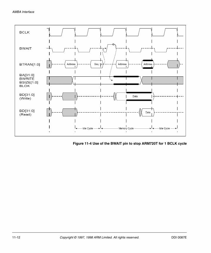
AMBA Interface
Figure 11-4 Use of the BWAIT pin to stop ARM720T for 1 BCLK cycle
11-12 Copyright © 1997, 1998 ARM Limited. All rights reserved. DDI 0087E
AMBA Interface
11.7 Maximum Sequential Length
The ARM720T may perform sequential memory accesses whenever the cycle is of the same type as the previous cycle (for example, read/write), and the addresses are consecutive. However, sequential accesses are interrupted on a 256-word boundary.
If a sequential access is performed over a 256-word boundary, the access to word 256 is turned into a non-sequential access, and further accesses continue sequentially as before.
This simplifies the design of the memory controller. Provided that peripherals and areas of memory are aligned to 256-word boundaries, sequential bursts are always local to one peripheral or memory device. This means that all accesses to a device always start with a non-sequential access.
A DRAM controller can take advantage of the fact that sequential cycles are always within a DRAM page, provided the page size is greater than 256.
DDI 0087E Copyright © 1997, 1998 ARM Limited. All rights reserved. 11-13
AMBA Interface
11.8 Read-Lock-Write
The read-lock-write sequence is generated by a SWP instruction.
The BLOK signal indicates that the two accesses should be treated as an atomic unit. A memory controller should ensure that no other bus activity is allowed to happen between the accesses when BLOK is asserted. When the ARM has started a read-lock-write sequence, it cannot be interrupted until it has completed.
On the bus, the sequence consists of:
• a read access
• a write access to the same address
This sequence is differentiated by the BLOK signal. BLOK:
• goes HIGH in the HIGH phase of BCLK at the start of the read access.
• always goes LOW at the end of the write access.
The read cycle is always performed as a single, non-sequential, external read cycle, regardless of the contents of the cache.
The write is forced to be unbuffered, so that it can be aborted if necessary.
The cache is updated on the write.
11-14 Copyright © 1997, 1998 ARM Limited. All rights reserved. DDI 0087E

AMBA Interface
11.9 Big-Endian / Little-Endian Operation
The ARM720T treats words in memory as being stored in big-endian or little-endian format depending on the value of the bigend bit in the control register, see Memory Formats on page 3-3.
Load and store are the only instructions affected by the endianness. Refer to the ARM Architecture Reference Manual for details of the LDR and STR instructions.
Little-endian format
In little-endian format:
• the lowest-numbered byte in a word is considered to be the least significant byte of the word.
• the highest-numbered byte is the most significant.
Byte 0 of the memory system should be connected to data lines 7 through 0 (BD[7:0]) in this format.
Figure 11-5 Little-endian addresses of bytes within word
Big-endian format
In big-endian format:
• the most significant byte of a word is stored at the lowest-numbered byte.
• the least significant byte is stored at the highest-numbered byte.
Byte 0 of the memory system should therefore be connected to data lines 31 through 24 (BD[31:24]).
DDI 0087E Copyright © 1997, 1998 ARM Limited. All rights reserved. 11-15
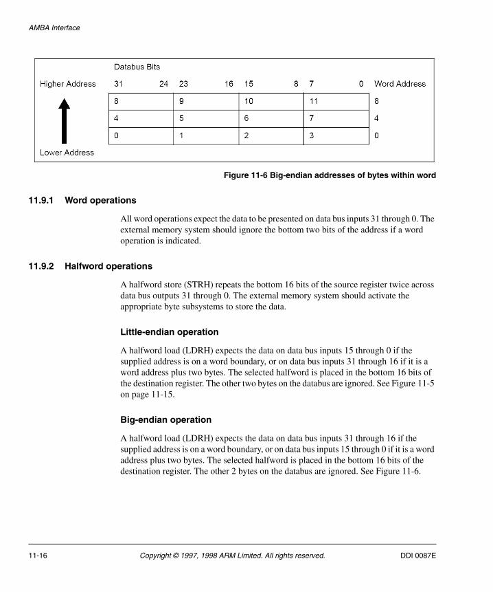
AMBA Interface
Figure 11-6 Big-endian addresses of bytes within word
11.9.1 Word operations
All word operations expect the data to be presented on data bus inputs 31 through 0. The external memory system should ignore the bottom two bits of the address if a word operation is indicated.
11.9.2 Halfword operations
A halfword store (STRH) repeats the bottom 16 bits of the source register twice across data bus outputs 31 through 0. The external memory system should activate the appropriate byte subsystems to store the data.
Little-endian operation
A halfword load (LDRH) expects the data on data bus inputs 15 through 0 if the supplied address is on a word boundary, or on data bus inputs 31 through 16 if it is a word address plus two bytes. The selected halfword is placed in the bottom 16 bits of the destination register. The other two bytes on the databus are ignored. See Figure 11-5 on page 11-15.
Big-endian operation
A halfword load (LDRH) expects the data on data bus inputs 31 through 16 if the supplied address is on a word boundary, or on data bus inputs 15 through 0 if it is a word address plus two bytes. The selected halfword is placed in the bottom 16 bits of the destination register. The other 2 bytes on the databus are ignored. See Figure 11-6.
11-16 Copyright © 1997, 1998 ARM Limited. All rights reserved. DDI 0087E

AMBA Interface
11.9.3 Byte operations
A byte store (STRB) repeats the bottom 8 bits of the source register four times across data bus outputs 31 through 0. The external memory system should activate the appropriate byte subsystem to store the data.
Because ARM720T duplicates the byte to be written across the databus and internally rotates bytes after reading them from the databus, a 32-bit memory system only needs to have control logic to enable the appropriate byte. There is no need to rotate or shift the data externally.
To ensure that all of the databus is driven during a byte read, it is valid to read a word back from the memory.
Little-endian operation
A byte load (LDRB) expects the data on data bus inputs 7 through 0 if the supplied address is on a word boundary, on data bus inputs 15 through 8 if it is a word address plus one byte, and so on. The selected byte is placed in the bottom 8 bits of the destination register. The other 3 bytes on the databus are ignored. See Figure 11-5 on page 11-15.
Big-endian operation
A byte load (LDRB) expects the data on data bus inputs 31 through 24 if the supplied address is on a word boundary, on data bus inputs 23 through 16 if it is a word address plus one byte, and so on. The selected byte is placed in the bottom 8 bits of the destination register. The other three bytes on the databus are ignored. See Figure 11-6 on page 11-16.
DDI 0087E Copyright © 1997, 1998 ARM Limited. All rights reserved. 11-17
AMBA Interface
11.10 Multi-master Operation
The AMBA bus specification supports multiple bus masters on the high performance Advanced System Bus (ASB). A simple two wire request/grant mechanism is implemented between the arbiter and each bus master. The arbiter ensures that only one bus master is active on the bus and also ensures that when no masters are requesting the bus, a default master is granted.
The specification also supports a shared lock signal. This allows bus masters to indicate that the current transfer is indivisible from the following transfer and prevents other bus masters from gaining access to the bus until the locked transfers have completed.
11.10.1 Arbitration
Efficient arbitration is important to reduce “dead-time” between successive masters being active on the bus. The bus protocol supports pipelined arbitration, such that arbitration for the next transfer is performed during the current transfer.
The arbitration protocol is defined, but the prioritization is flexible and left to the application. Typically, the Test Interface would be given the highest priority to ensure test access under all conditions. Every system must also include a default bus master, which is granted the bus when no bus masters are requesting it.
The request signal, AREQ, from each bus master to the arbiter indicates that the bus master requires the bus. The grant signal from the arbiter to the bus master, AGNT, indicates that the bus master is currently the highest priority master requesting the bus.
The bus master:
• must drive the BTRAN signals during BCLK HIGH when AGNT is HIGH.
• will become granted when AGNT is HIGH and BWAIT is LOW on a rising edge of BCLK.
The shared bus lock signal, BLOK, indicates to the arbiter that the following transfer is indivisible from the current transfer and no other bus master should be given access to the bus.
A bus master must always drive a valid level on the BLOK signal when granted the bus to ensure the arbitration process can continue, even if the bus master is not performing any transfers.
The arbiter functions as follows:
1. Bus masters assert AREQ during the HIGH phase of BCLK.
2. The arbiter samples all AREQ signals on the falling edge of BCLK.
11-18 Copyright © 1997, 1998 ARM Limited. All rights reserved. DDI 0087E
AMBA Interface
3. During the LOW phase of BCLK, the arbiter also samples the BLOK signal and then asserts the appropriate AGNT signal.
If BLOK is LOW, the arbiter grants the highest priority bus master.
If BLOK is HIGH, the arbiter keeps the same bus master granted.
The arbiter can update the grant signals every bus cycle; however, a new bus master can only become granted and start driving the bus when the current transfer completes, as indicated by BWAIT being LOW. Therefore, it is possible for the potential next bus master to change during waited transfers.
The BLOK signal is ignored by the arbiter during the single cycle of handover between two different bus masters.
If no bus masters are requesting the bus, the arbiter must grant the default bus master. The arbitration protocol is defined, but the prioritization is flexible and left to the application. A simple fixed-priority scheme may be used; alternatively, a more complex scheme can be implemented if required by the application.
DDI 0087E Copyright © 1997, 1998 ARM Limited. All rights reserved. 11-19
AMBA Interface
11.11 Bus Master Handover
Bus master handover occurs when a bus master, which is not currently granted the bus, becomes the new granted bus master.
A bus master becomes granted when AGNT is HIGH and BWAIT is LOW. AGNT HIGH indicates the bus master is currently the highest priority master requesting the bus and BWAIT LOW indicates the previous transfer has completed. Figure 11-7 on page 11-21 shows the bus master handover process.
11-20 Copyright © 1997, 1998 ARM Limited. All rights reserved. DDI 0087E
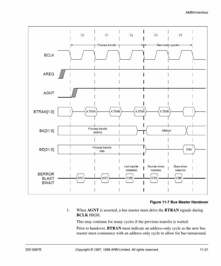
AMBA Interface
Figure 11-7 Bus Master Handover
1. When AGNT is asserted, a bus master must drive the BTRAN signals during BCLK HIGH.
This may continue for many cycles if the previous transfer is waited.
Prior to handover, BTRAN must indicate an address-only cycle as the new bus master must commence with an address-only cycle to allow for bus turnaround.
DDI 0087E Copyright © 1997, 1998 ARM Limited. All rights reserved. 11-21
AMBA Interface
2. When the previous transfer completes, the new bus master is granted.
3. In the last clock HIGH phase of the previous transfer, the address bus stops being driven by the previous bus master.
4. The new bus master starts to drive the address bus and control signals during the clock LOW phase.
5. The first transfer may then commence in the following bus cycle.
During a waited transfer, bus master handover may be delayed and it is possible that the AGNT to a particular bus master may be asserted and then negated, if another higher priority bus master then requests the bus before the current transfer has completed.
11-22 Copyright © 1997, 1998 ARM Limited. All rights reserved. DDI 0087E
AMBA Interface
11.12 Default Bus Master
Every system must be designed with a single default bus master, which is granted when no other bus master is requesting the bus. The default bus master is responsible for driving the following signals to ensure the bus remains active.
• BTRAN must be driven to indicate address-only transfer.
• BLOK must be driven LOW.
Note If the ARM720T is to be the default bus master then the AREQ signal from the ARM720T should not be used.
DDI 0087E Copyright © 1997, 1998 ARM Limited. All rights reserved. 11-23
AMBA Interface
11-24 Copyright © 1997, 1998 ARM Limited. All rights reserved. DDI 0087E

Chapter 12 AMBA Test
This chapter describes the test features of ARM720T.
• Slave Operation (Test mode) on page 12-2
• ARM720T Test Mode on page 12-4
• ARM7DMT Core Test Mode on page 12-6
• RAM Test Mode on page 12-7
• TAG Test Mode on page 12-8
• MMU Test Mode on page 12-10
• Test Register Mapping on page 12-12.
DDI 0087E Copyright © 1997, 1998 ARM Limited. All rights reserved. 12-1
AMBA Test
12.1 Slave Operation (Test mode)
When the block is selected as a slave, it is possible to write and read test vectors to the core using the AMBA test methodology.
The BTRAN provides 4 test modes for this purpose:
• ARM720T test mode
• ARM7DMT Core test mode
• RAM test mode
• TAG test mode
To apply test vectors to the ARM720T, the ARM720T block must have been deselected as a master (AGNT goes LOW). The Test Interface Controller becomes the bus master, and the ARM720T is selected as a slave using the signal DSELARM. This places the ARM720T into test mode, and allows access to the test registers.
The tests are sequenced by the test state machine in the AMBA interface, which generates the appropriate control signals for the test modes.
A sample test sequence is shown in Figure 12-1 on page 12-3.
12-2 Copyright © 1997, 1998 ARM Limited. All rights reserved. DDI 0087E
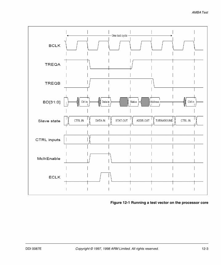
AMBA Test
Figure 12-1 Running a test vector on the processor core
DDI 0087E Copyright © 1997, 1998 ARM Limited. All rights reserved. 12-3
AMBA Test
12.2 ARM720T Test Mode
The ARM720T test mode is used to test the functionality of the:
• cache control logic
• write buffer
• protection unit
• cache
To perform this test control, stimuli are applied to the control register, see Table 12-3 on page 12-12.
Data packets are read or written as appropriate and the address and status are read back (see Table 12-3 on page 12-12.
The sequencing for this test mode is as shown in Figure 12-2 on page 12-5. This is the default test mode, and is selected when the bits [31:29] of the control register are set LOW (see Table 12-3 on page 12-12).
12-4 Copyright © 1997, 1998 ARM Limited. All rights reserved. DDI 0087E
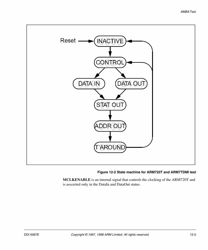
AMBA Test
Figure 12-2 State machine for ARM720T and ARM7TDMI test
MCLKENABLE is an internal signal that controls the clocking of the ARM720T and is asscerted only in the DataIn and DataOut status.
DDI 0087E Copyright © 1997, 1998 ARM Limited. All rights reserved. 12-5
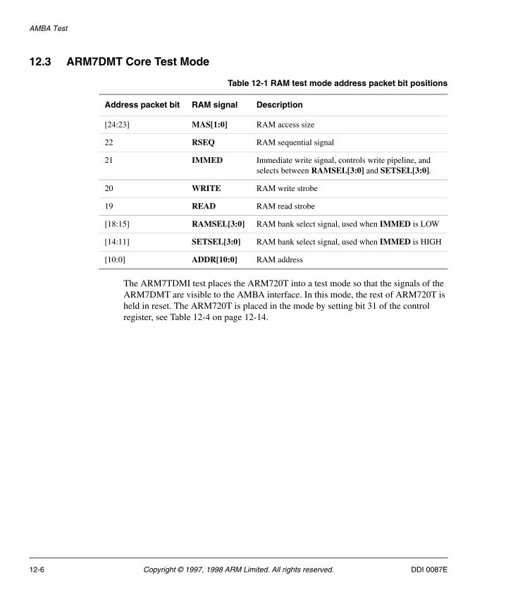
AMBA Test
12.3 ARM7DMT Core Test Mode
The ARM7TDMI test places the ARM720T into a test mode so that the signals of the ARM7DMT are visible to the AMBA interface. In this mode, the rest of ARM720T is held in reset. The ARM720T is placed in the mode by setting bit 31 of the control register, see Table 12-4 on page 12-14.
Table 12-1 RAM test mode address packet bit positions
Address packet bit RAM signal Description
[24:23] MAS[1:0] RAM access size
22 RSEQ RAM sequential signal
21 IMMED Immediate write signal, controls write pipeline, and selects between RAMSEL[3:0] and SETSEL[3:0].
20 WRITE RAM write strobe
19 READ RAM read strobe
[18:15] RAMSEL[3:0] RAM bank select signal, used when IMMED is LOW
[14:11] SETSEL[3:0] RAM bank select signal, used when IMMED is HIGH
[10:0] ADDR[10:0] RAM address
12-6 Copyright © 1997, 1998 ARM Limited. All rights reserved. DDI 0087E
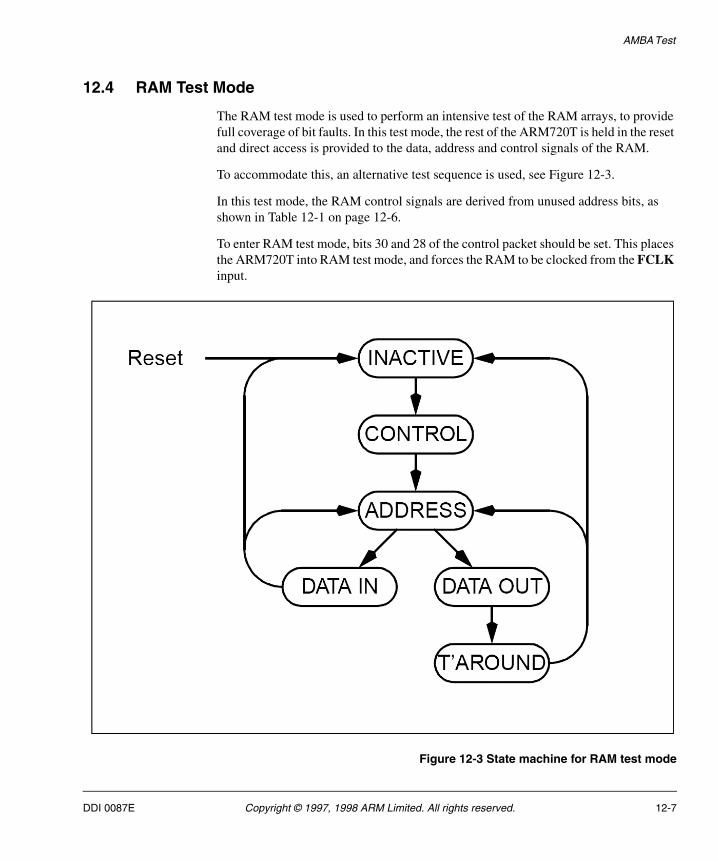
AMBA Test
12.4 RAM Test Mode
The RAM test mode is used to perform an intensive test of the RAM arrays, to provide full coverage of bit faults. In this test mode, the rest of the ARM720T is held in the reset and direct access is provided to the data, address and control signals of the RAM.
To accommodate this, an alternative test sequence is used, see Figure 12-3.
In this test mode, the RAM control signals are derived from unused address bits, as shown in Table 12-1 on page 12-6.
To enter RAM test mode, bits 30 and 28 of the control packet should be set. This places the ARM720T into RAM test mode, and forces the RAM to be clocked from the FCLK input.
Figure 12-3 State machine for RAM test mode
DDI 0087E Copyright © 1997, 1998 ARM Limited. All rights reserved. 12-7
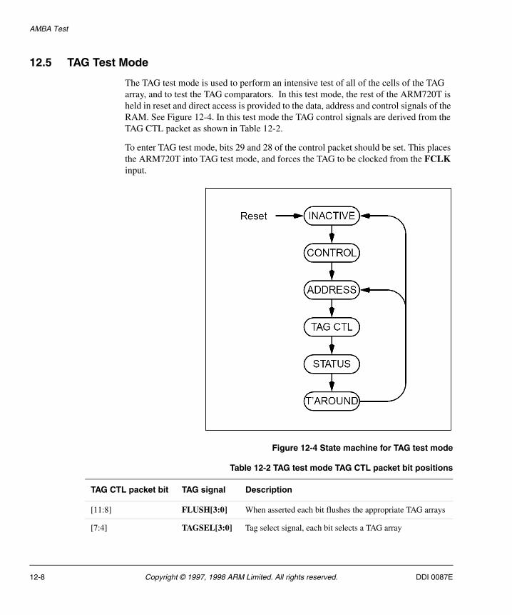
AMBA Test
12.5 TAG Test Mode
The TAG test mode is used to perform an intensive test of all of the cells of the TAG array, and to test the TAG comparators. In this test mode, the rest of the ARM720T is held in reset and direct access is provided to the data, address and control signals of the RAM. See Figure 12-4. In this test mode the TAG control signals are derived from the TAG CTL packet as shown in Table 12-2.
To enter TAG test mode, bits 29 and 28 of the control packet should be set. This places the ARM720T into TAG test mode, and forces the TAG to be clocked from the FCLK input.
Figure 12-4 State machine for TAG test mode
Table 12-2 TAG test mode TAG CTL packet bit positions
TAG CTL packet bit TAG signal Description
[11:8] FLUSH[3:0] When asserted each bit flushes the appropriate TAG arrays
[7:4] TAGSEL[3:0] Tag select signal, each bit selects a TAG array
12-8 Copyright © 1997, 1998 ARM Limited. All rights reserved. DDI 0087E
AMBA Test
2 WRITE TAG write strobe
1 READ TAG read strobe
0 VALID Valid input, the value on VALID is written into the valid cell in the array on a write.
Table 12-2 TAG test mode TAG CTL packet bit positions (continued)
TAG CTL packet bit TAG signal Description
DDI 0087E Copyright © 1997, 1998 ARM Limited. All rights reserved. 12-9
AMBA Test
12.6 MMU Test Mode
The MMU Test Mode is used to perform an intensive test of all the cells in the TLB array and to test the protection mechanism. In this test mode the rest of the ARM720T is held in reset and direct access is provided to the data, control and translated address of the MMU. See Figure 12-5 on page 12-11.
In this test mode, the MMU Control Signals are derived from the MMU CM packet.
To enter MMU test mode, bits 28 and 27 of the control packet should be set. This places the ARM720T into MMU test mode and forces the MMU to be clocked from the FCLK input.
12-10 Copyright © 1997, 1998 ARM Limited. All rights reserved. DDI 0087E
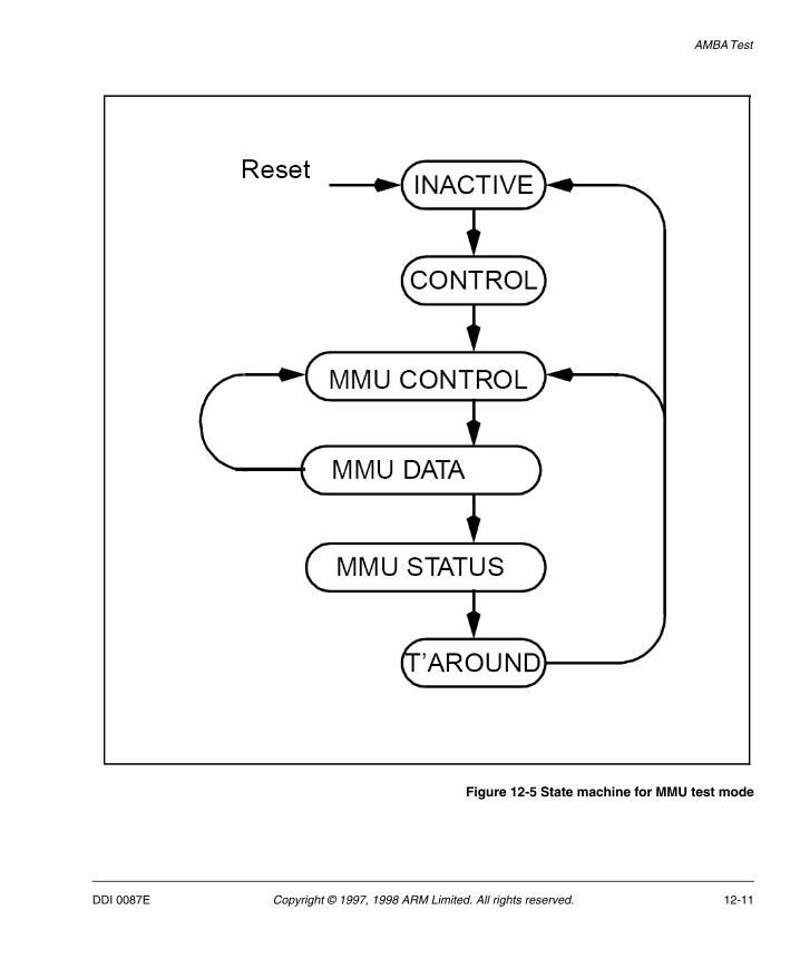
AMBA Test
Figure 12-5 State machine for MMU test mode
DDI 0087E Copyright © 1997, 1998 ARM Limited. All rights reserved. 12-11
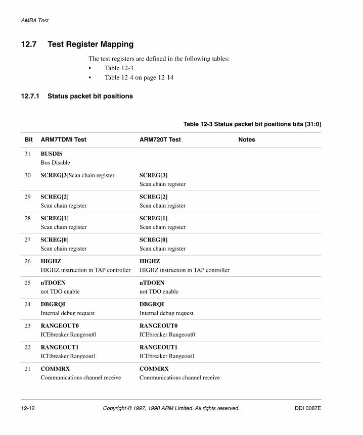
AMBA Test
12.7 Test Register Mapping
The test registers are defined in the following tables:
• Table 12-3
• Table 12-4 on page 12-14
12.7.1 Status packet bit positions
Table 12-3 Status packet bit positions bits [31:0]
Bit ARM7TDMI Test ARM720T Test Notes
31 BUSDISBus Disable
30 SCREG[3]Scan chain register SCREG[3]
Scan chain register
29 SCREG[2]
Scan chain register
SCREG[2]
Scan chain register
28 SCREG[1]Scan chain register
SCREG[1]Scan chain register
27 SCREG[0]
Scan chain register
SCREG[0]
Scan chain register
26 HIGHZ
HIGHZ instruction in TAP controller
HIGHZ
HIGHZ instruction in TAP controller
25 nTDOENnot TDO enable
nTDOENnot TDO enable
24 DBGRQI
Internal debug request
DBGRQI
Internal debug request
23 RANGEOUT0
ICEbreaker Rangeout0
RANGEOUT0
ICEbreaker Rangeout0
22 RANGEOUT1
ICEbreaker Rangeout1
RANGEOUT1
ICEbreaker Rangeout1
21 COMMRX
Communications channel receive
COMMRX
Communications channel receive
12-12 Copyright © 1997, 1998 ARM Limited. All rights reserved. DDI 0087E
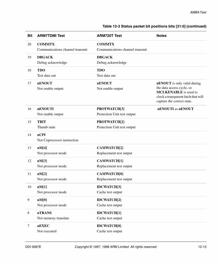
AMBA Test
20 COMMTXCommunications channel transmit
COMMTXCommunications channel transmit
19 DBGACK
Debug acknowledge
DBGACK
Debug acknowledge
18 TDO
Test data out
TDO
Test data out
17 nENOUTNot enable output.
nENOUTNot enable output
nENOUT is only valid during the data access cycle, so MCLKENABLE is used to clock a transparent latch that will capture the correct state.
16 nENOUTINot enable output
PROTWATCH[3]Protection Unit test output
nENOUTI as nENOUT
15 TBIT
Thumb state
PROTWATCH[2]
Protection Unit test output
14 nCPI
Not Coprocessor instruction
13 nM[4]Not processor mode
CAMWATCH[2]Replacement test output
12 nM[3]
Not processor mode
CAMWATCH[1]
Replacement test output
11 nM[2]
Not processor mode
CAMWATCH[0]
Replacement test output
10 nM[1]Not processor mode
IDCWATCH[3]Cache test output
9 nM[0]
Not processor mode
IDCWATCH[2]
Cache test output
8 nTRANSNot memory translate
IDCWATCH[1]Cache test output
7 nEXEC
Not executed
IDCWATCH[0]
Cache test output
Table 12-3 Status packet bit positions bits [31:0] (continued)
Bit ARM7TDMI Test ARM720T Test Notes
DDI 0087E Copyright © 1997, 1998 ARM Limited. All rights reserved. 12-13
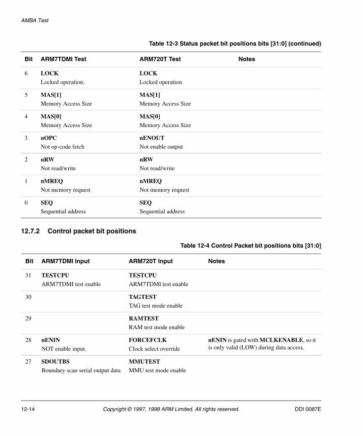
AMBA Test
12.7.2 Control packet bit positions
6 LOCKLocked operation.
LOCKLocked operation
5 MAS[1]
Memory Access Size
MAS[1]
Memory Access Size
4 MAS[0]
Memory Access Size
MAS[0]
Memory Access Size
3 nOPCNot op-code fetch
nENOUTNot enable output
2 nRW
Not read/write
nRW
Not read/write
1 nMREQ
Not memory request
nMREQ
Not memory request
0 SEQSequential address
SEQSequential address
Table 12-4 Control Packet bit positions bits [31:0]
Bit ARM7TDMI Input ARM720T Input Notes
31 TESTCPUARM7TDMI test enable
TESTCPUARM7TDMI test enable
30 TAGTEST
TAG test mode enable
29 RAMTEST
RAM test mode enable
28 nENIN
NOT enable input.
FORCEFCLK
Clock select override
nENIN is gated with MCLKENABLE, so it is only valid (LOW) during data access.
27 SDOUTBS
Boundary scan serial output data
MMUTEST
MMU test mode enable
Table 12-3 Status packet bit positions bits [31:0] (continued)
Bit ARM7TDMI Test ARM720T Test Notes
12-14 Copyright © 1997, 1998 ARM Limited. All rights reserved. DDI 0087E
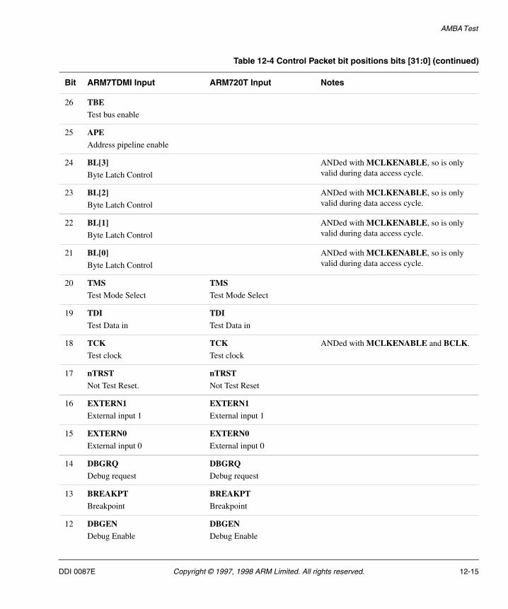
AMBA Test
26 TBETest bus enable
25 APE
Address pipeline enable
24 BL[3]
Byte Latch Control
ANDed with MCLKENABLE, so is only valid during data access cycle.
23 BL[2]Byte Latch Control
ANDed with MCLKENABLE, so is only valid during data access cycle.
22 BL[1]
Byte Latch Control
ANDed with MCLKENABLE, so is only valid during data access cycle.
21 BL[0]
Byte Latch Control
ANDed with MCLKENABLE, so is only valid during data access cycle.
20 TMSTest Mode Select
TMSTest Mode Select
19 TDI
Test Data in
TDI
Test Data in
18 TCK
Test clock
TCK
Test clock
ANDed with MCLKENABLE and BCLK.
17 nTRSTNot Test Reset.
nTRSTNot Test Reset
16 EXTERN1
External input 1
EXTERN1
External input 1
15 EXTERN0
External input 0
EXTERN0
External input 0
14 DBGRQDebug request
DBGRQDebug request
13 BREAKPT
Breakpoint
BREAKPT
Breakpoint
12 DBGENDebug Enable
DBGENDebug Enable
Table 12-4 Control Packet bit positions bits [31:0] (continued)
Bit ARM7TDMI Input ARM720T Input Notes
DDI 0087E Copyright © 1997, 1998 ARM Limited. All rights reserved. 12-15
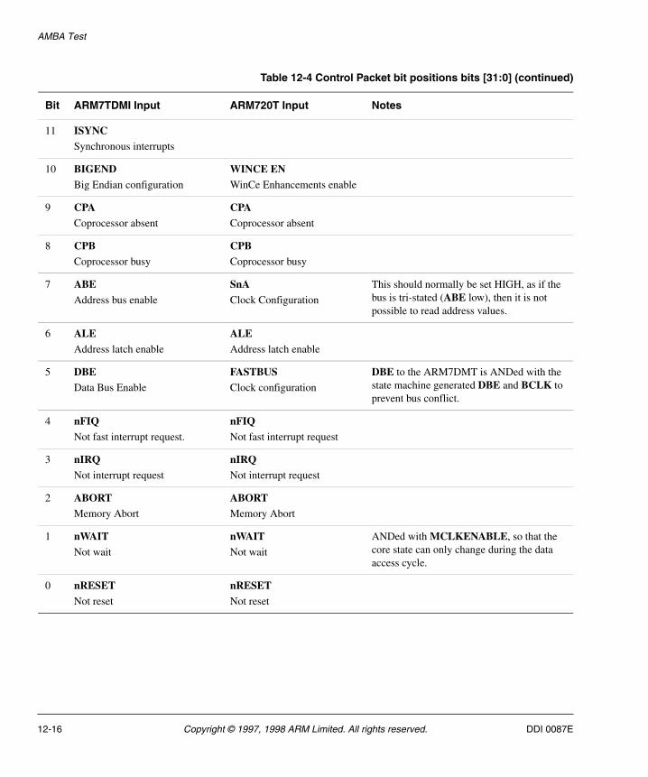
AMBA Test
11 ISYNCSynchronous interrupts
10 BIGEND
Big Endian configuration
WINCE EN
WinCe Enhancements enable
9 CPA
Coprocessor absent
CPA
Coprocessor absent
8 CPBCoprocessor busy
CPBCoprocessor busy
7 ABE
Address bus enable
SnA
Clock Configuration
This should normally be set HIGH, as if the bus is tri-stated (ABE low), then it is not possible to read address values.
6 ALE
Address latch enable
ALE
Address latch enable
5 DBEData Bus Enable
FASTBUSClock configuration
DBE to the ARM7DMT is ANDed with the state machine generated DBE and BCLK to prevent bus conflict.
4 nFIQ
Not fast interrupt request.
nFIQ
Not fast interrupt request
3 nIRQ
Not interrupt request
nIRQ
Not interrupt request
2 ABORTMemory Abort
ABORTMemory Abort
1 nWAIT
Not wait
nWAIT
Not wait
ANDed with MCLKENABLE, so that the core state can only change during the data access cycle.
0 nRESET
Not reset
nRESET
Not reset
Table 12-4 Control Packet bit positions bits [31:0] (continued)
Bit ARM7TDMI Input ARM720T Input Notes
12-16 Copyright © 1997, 1998 ARM Limited. All rights reserved. DDI 0087E


![EECS 373 - University of Michiganweb.eecs.umich.edu/~prabal/teaching/eecs373-w15/slides/lec2-6up.pdf · EECS 373 Design of ... [ARM TRM] ARM DDI 0337E, “Cortex-M3 Technical Reference](https://img.pdfslide.net/doc/110x75/5af6d69f7f8b9a154c919139/eecs-373-university-of-prabalteachingeecs373-w15slideslec2-6uppdfeecs-373.jpg)