Embed Size (px)
Citation preview
Arm® Corstone™ SSE-300 with Ethos™-U55 Example Subsystem for MPS3
Revision: B
Application Note AN547 Non-Confidential Issue B Copyright © 2020, 2021 Arm Limited (or its affiliates). All rights reserved.
DAI 0547B
Arm® Corstone™ SSE-300 with Ethos™-U55 Example Subsystem for MPS3 - Application Note AN547
DAI 0547B Issue B
Copyright © 2020, 2021 Arm Limited (or its affiliates). All rights reserved. Non-Confidential
Page 2 of 53
Arm® Corstone™ SSE-300 with Ethos™-U55 Example Subsystem for MPS3
Application Note AN547
Copyright © 2020, 2021 Arm Limited (or its affiliates). All rights reserved.
Release information
Document history
Issue Date Confidentiality Change
A 30th November 2020 Confidential First Issue
B 29th January 2021 Non-Confidential Confidentiality status changed to Non-Confidential
Non-Confidential Proprietary Notice
This document is protected by copyright and other related rights and the practice or implementation of the information contained in this document may be protected by one or more patents or pending patent applications. No part of this document may be reproduced in any form by any means without the express prior written permission of Arm. No license, express or implied, by estoppel or otherwise to any intellectual property rights is granted by this document unless specifically stated.
Your access to the information in this document is conditional upon your acceptance that you will not use or permit others to use the information for the purposes of determining whether implementations infringe any third party patents.
THIS DOCUMENT IS PROVIDED “AS IS”. ARM PROVIDES NO REPRESENTATIONS AND NO WARRANTIES, EXPRESS, IMPLIED OR STATUTORY, INCLUDING, WITHOUT LIMITATION, THE IMPLIED WARRANTIES OF MERCHANTABILITY, SATISFACTORY QUALITY, NON-INFRINGEMENT OR FITNESS FOR A PARTICULAR PURPOSE WITH RESPECT TO THE DOCUMENT. For the avoidance of doubt, Arm makes no representation with respect to, and has undertaken no analysis to identify or understand the scope and content of, patents, copyrights, trade secrets, or other rights.
This document may include technical inaccuracies or typographical errors.
TO THE EXTENT NOT PROHIBITED BY LAW, IN NO EVENT WILL ARM BE LIABLE FOR ANY DAMAGES, INCLUDING WITHOUT LIMITATION ANY DIRECT, INDIRECT, SPECIAL, INCIDENTAL, PUNITIVE, OR CONSEQUENTIAL DAMAGES, HOWEVER CAUSED AND REGARDLESS OF THE THEORY OF LIABILITY, ARISING OUT OF ANY USE OF THIS DOCUMENT, EVEN IF ARM HAS BEEN ADVISED OF THE POSSIBILITY OF SUCH DAMAGES.
This document consists solely of commercial items. You shall be responsible for ensuring that any use, duplication or disclosure of this document complies fully with any relevant export laws and regulations to assure that this document or any portion thereof is not exported, directly or indirectly, in violation of such export laws. Use of the word “partner” in reference to Arm's customers is not intended to create or refer to any partnership relationship with any other company. Arm may make changes to this document at any time and without notice.
If any of the provisions contained in these terms conflict with any of the provisions of any click through or signed written agreement covering this document with Arm, then the click through or signed written agreement prevails over and supersedes the conflicting provisions of these terms. This document may be translated into other languages for convenience, and you agree that if there is any conflict between the English version of this document and any translation, the terms of the English version of the Agreement shall prevail.
The Arm corporate logo and words marked with ® or ™ are registered trademarks or trademarks of Arm Limited (or its affiliates) in the US and/or elsewhere. All rights reserved. Other brands and names mentioned in this
Arm® Corstone™ SSE-300 with Ethos™-U55 Example Subsystem for MPS3 - Application Note AN547
DAI 0547B Issue B
Copyright © 2020, 2021 Arm Limited (or its affiliates). All rights reserved. Non-Confidential
Page 3 of 53
document may be the trademarks of their respective owners. Please follow Arm's trademark usage guidelines at http://www.arm.com/company/policies/trademarks.
Copyright © 2020, 2021 Arm Limited (or its affiliates). All rights reserved.
Arm Limited. Company 02557590 registered in England.
110 Fulbourn Road, Cambridge, England CB1 9NJ.
(LES-PRE-20349)
Confidentiality Status
This document is Non-Confidential. The right to use, copy and disclose this document may be subject to license restrictions in accordance with the terms of the agreement entered into by Arm and the party that Arm delivered this document to.
Unrestricted Access is an Arm internal classification.
Product Status
The information in this document is Final, that is for a developed product.
Web Address
developer.arm.com
Progressive terminology commitment
Arm values inclusive communities. Arm recognizes that we and our industry have used terms that can be offensive. Arm strives to lead the industry and create change.
This document includes terms that can be offensive. We will replace these terms in a future issue of this document. If you find offensive terms in this document, please email [email protected].
Arm® Corstone™ SSE-300 with Ethos™-U55 Example Subsystem for MPS3 - Application Note AN547
DAI 0547B Issue B
Copyright © 2020, 2021 Arm Limited (or its affiliates). All rights reserved. Non-Confidential
Page 4 of 53
LICENCE GRANTS
THE END USER LICENCE AGREEMENT FOR THE ARM SYSTEM OR SUBSYSTEM FOR AN ARM FPGA PROTOTYPING BOARD (“THE LICENCE”), LES-PRE-21902, DEFINES THE LICENCE GRANTS.
DELIVERABLES
Part A Hardware Binaries: Encrypted FPGA bitstream file containing various the Arm technology including:
SSE-300 Subsystem Cortex-M55 Processor Ethos-U55 Embedded ML Inference processor.
Software Binaries: Motherboard Configuration Controller binary (mbb_vxxx.ebf), including Keil USB and SD card drivers, and Analog Devices FMC EEPROM reader. selftest binary (an547_st.axf) for Cortex-M55 in Corstone™ SSE-300. Documentation: Documentation, provided as PDF Part B Text configuration files (.txt) in the <install_dir>/Boardfiles/MB/HBI0309x/ directory: /board.txt
/AN547/an547_v1.txt
/AN547/images.txt
Part C None Part D None
Arm® Corstone™ SSE-300 with Ethos™-U55 Example Subsystem for MPS3 - Application Note AN547
DAI 0547B Issue B
Copyright © 2020, 2021 Arm Limited (or its affiliates). All rights reserved. Non-Confidential
Page 5 of 53
Contents
1 Introduction ........................................................................................................................................................... 8
1.1 Intended audience .................................................................................................................................................... 8
1.2 Conventions ............................................................................................................................................................... 8
1.2.1 Glossary .................................................................................................................................................................... 8
1.2.2 Typographical conventions ............................................................................................................................... 9
1.3 Additional reading .................................................................................................................................................... 9
1.4 Feedback.................................................................................................................................................................... 10
1.4.1 Feedback on this product ................................................................................................................................. 10
1.4.2 Feedback on content ......................................................................................................................................... 10
1.4.3 Other information .............................................................................................................................................. 11
2 Preface .................................................................................................................................................................. 12
2.1 Purpose of this application note ........................................................................................................................ 12
2.2 Terms and abbreviations ..................................................................................................................................... 12
2.3 Arm IP version details ........................................................................................................................................... 13
2.4 Encryption key ......................................................................................................................................................... 13
3 Overview .............................................................................................................................................................. 14
3.1 System block diagram ........................................................................................................................................... 14
3.2 Arm® Corstone™ SSE-300 with Ethos™-U55 Example Subsystem ..................................................... 15
3.3 SIE-300 Components ............................................................................................................................................ 16
3.4 SIE-200 Components ............................................................................................................................................ 16
3.5 Corelink™ XHB-500 ............................................................................................................................................... 16
3.6 Memory Protection ............................................................................................................................................... 16
3.7 Memory Map Overview ....................................................................................................................................... 17
3.8 Expansion System peripherals ........................................................................................................................... 20
3.8.1 MSTEXPPILL Peripheral Map ......................................................................................................................... 20
3.8.2 MSTEXPPIHL Peripheral Map ........................................................................................................................ 22
4 Programmers Model ......................................................................................................................................... 24
4.1 ITCM ........................................................................................................................................................................... 24
4.2 FPGA SRAM ............................................................................................................................................................. 24
4.3 DTCM ......................................................................................................................................................................... 24
4.4 QSPI ............................................................................................................................................................................. 24
Arm® Corstone™ SSE-300 with Ethos™-U55 Example Subsystem for MPS3 - Application Note AN547
DAI 0547B Issue B
Copyright © 2020, 2021 Arm Limited (or its affiliates). All rights reserved. Non-Confidential
Page 6 of 53
4.5 DDR4 .......................................................................................................................................................................... 24
4.6 AHB GPIO ................................................................................................................................................................. 25
4.7 SPI ................................................................................................................................................................................ 25
4.8 SBCon (I2C) ............................................................................................................................................................... 25
4.9 UART ........................................................................................................................................................................... 26
4.10 Color LCD parallel interface ............................................................................................................................ 26
4.11 Ethernet .................................................................................................................................................................. 27
4.12 USB............................................................................................................................................................................ 27
4.13 Real Time Clock, RTC.......................................................................................................................................... 27
4.14 Audio I2S .................................................................................................................................................................. 28
4.15 Audio Configuration ........................................................................................................................................... 29
4.16 FPGA system control and I/O .......................................................................................................................... 30
4.17 Serial Communication Controller (SCC) ...................................................................................................... 31
5 Clock architecture ............................................................................................................................................. 33
5.1 Clocks.......................................................................................................................................................................... 33
5.1.1 Source clocks ........................................................................................................................................................ 33
5.1.2 Generated clocks ................................................................................................................................................ 33
6 FPGA Secure Privilege Control ...................................................................................................................... 34
7 Interrupt Map ...................................................................................................................................................... 37
UART Interrupts............................................................................................................................................................. 39
8 Shield Support ..................................................................................................................................................... 40
9 Using AN547 on the MPS3 Board ................................................................................................................. 42
9.1 Pre-Requisites ......................................................................................................................................................... 42
9.2 Loading a prebuilt image onto the MPS3 Board .......................................................................................... 42
9.3 UART Serial Ports ................................................................................................................................................... 43
9.4 UART Serial Port Terminal Emulator Settings ............................................................................................. 43
9.5 MPS3 USB Serial port drivers for Windows .................................................................................................. 43
10 Software ............................................................................................................................................................. 44
10.1 Rebuilding software ............................................................................................................................................ 44
10.2 Loading software on the MPS3 board .......................................................................................................... 44
11 Debug .................................................................................................................................................................. 45
Arm® Corstone™ SSE-300 with Ethos™-U55 Example Subsystem for MPS3 - Application Note AN547
DAI 0547B Issue B
Copyright © 2020, 2021 Arm Limited (or its affiliates). All rights reserved. Non-Confidential
Page 7 of 53
11.1 Debug support for Keil MDK ........................................................................................................................... 45
11.2 Trace support for Keil MDK ............................................................................................................................. 46
11.3 Debug and Trace support for Arm Development Studio ....................................................................... 47
11.3.1 Establishing a Debug Session ....................................................................................................................... 47
11.3.2 Trace in Debug session ................................................................................................................................... 51
Arm® Corstone™ SSE-300 with Ethos™-U55 Example Subsystem for MPS3 - Application Note AN547
DAI 0547B Issue B
1 Introduction
Copyright © 2020, 2021 Arm Limited (or its affiliates). All rights reserved. Non-Confidential
Page 8 of 53
1 Introduction
1.1 Intended audience
This application note document is written for experienced hardware, System-on-Chip (SoC) and software engineers who might or might not have experience with Arm products. Such engineers typically have experience in writing Verilog and of performing synthesis but might have limited experience of integrating and implementing Arm products.
1.2 Conventions
The following subsections describe conventions used in Arm documents.
1.2.1 Glossary
The Arm Glossary is a list of terms used in Arm documentation, together with definitions for those terms. The Arm Glossary does not contain terms that are industry standard unless the Arm meaning differs from the generally accepted meaning.
See the Arm Glossary for more information: https://developer.arm.com/glossary.
Arm® Corstone™ SSE-300 with Ethos™-U55 Example Subsystem for MPS3 - Application Note AN547
DAI 0547B Issue B
1 Introduction
Copyright © 2020, 2021 Arm Limited (or its affiliates). All rights reserved. Non-Confidential
Page 9 of 53
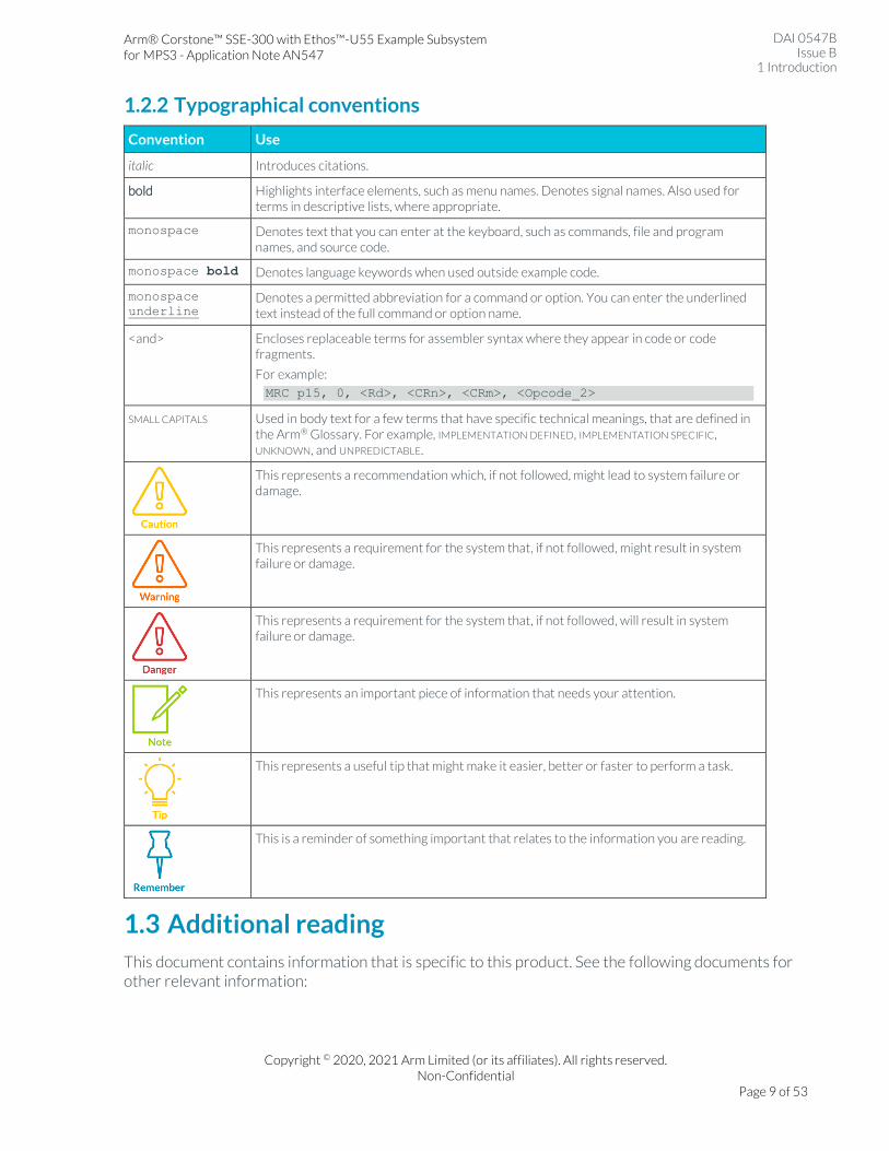
1.2.2 Typographical conventions
Convention Use
italic Introduces citations.
bold Highlights interface elements, such as menu names. Denotes signal names. Also used for terms in descriptive lists, where appropriate.
monospace Denotes text that you can enter at the keyboard, such as commands, file and program names, and source code.
monospace bold Denotes language keywords when used outside example code.
monospace
underline Denotes a permitted abbreviation for a command or option. You can enter the underlined text instead of the full command or option name.
<and> Encloses replaceable terms for assembler syntax where they appear in code or code fragments.
For example:
MRC p15, 0, <Rd>, <CRn>, <CRm>, <Opcode_2>
SMALL CAPITALS Used in body text for a few terms that have specific technical meanings, that are defined in the Arm® Glossary. For example, IMPLEMENTATION DEFINED, IMPLEMENTATION SPECIFIC, UNKNOWN, and UNPREDICTABLE.
This represents a recommendation which, if not followed, might lead to system failure or damage.
This represents a requirement for the system that, if not followed, might result in system failure or damage.
This represents a requirement for the system that, if not followed, will result in system failure or damage.
This represents an important piece of information that needs your attention.
This represents a useful tip that might make it easier, better or faster to perform a task.
This is a reminder of something important that relates to the information you are reading.
1.3 Additional reading
This document contains information that is specific to this product. See the following documents for other relevant information:
Arm® Corstone™ SSE-300 with Ethos™-U55 Example Subsystem for MPS3 - Application Note AN547
DAI 0547B Issue B
1 Introduction
Copyright © 2020, 2021 Arm Limited (or its affiliates). All rights reserved. Non-Confidential
Page 10 of 53
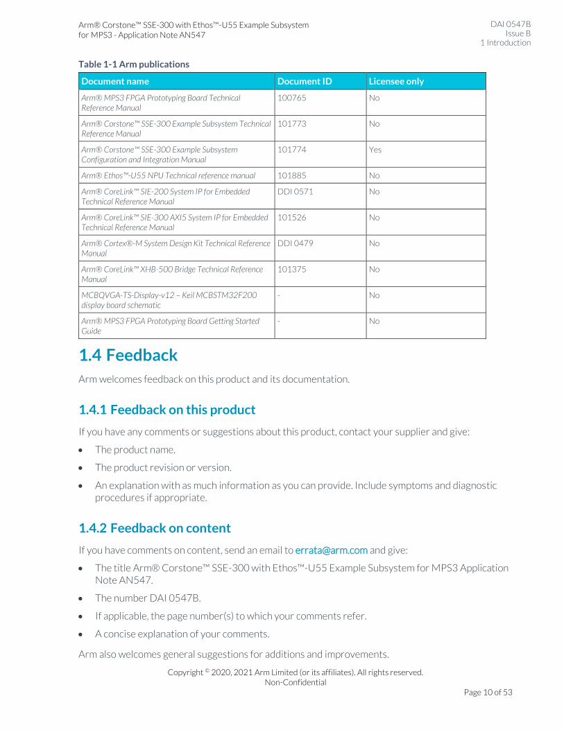
Table 1-1 Arm publications
Document name Document ID Licensee only
Arm® MPS3 FPGA Prototyping Board Technical Reference Manual
100765 No
Arm® Corstone™ SSE-300 Example Subsystem Technical Reference Manual
101773 No
Arm® Corstone™ SSE-300 Example Subsystem Configuration and Integration Manual
101774 Yes
Arm® Ethos™-U55 NPU Technical reference manual 101885 No
Arm® CoreLink™ SIE-200 System IP for Embedded Technical Reference Manual
DDI 0571 No
Arm® CoreLink™ SIE-300 AXI5 System IP for Embedded Technical Reference Manual
101526 No
Arm® Cortex®-M System Design Kit Technical Reference Manual
DDI 0479 No
Arm® CoreLink™ XHB-500 Bridge Technical Reference Manual
101375 No
MCBQVGA-TS-Display-v12 – Keil MCBSTM32F200 display board schematic
- No
Arm® MPS3 FPGA Prototyping Board Getting Started Guide
- No
1.4 Feedback
Arm welcomes feedback on this product and its documentation.
1.4.1 Feedback on this product
If you have any comments or suggestions about this product, contact your supplier and give:
• The product name.
• The product revision or version.
• An explanation with as much information as you can provide. Include symptoms and diagnostic procedures if appropriate.
1.4.2 Feedback on content
If you have comments on content, send an email to [email protected] and give:
• The title Arm® Corstone™ SSE-300 with Ethos™-U55 Example Subsystem for MPS3 Application Note AN547.
• The number DAI 0547B.
• If applicable, the page number(s) to which your comments refer.
• A concise explanation of your comments.
Arm also welcomes general suggestions for additions and improvements.
Arm® Corstone™ SSE-300 with Ethos™-U55 Example Subsystem for MPS3 - Application Note AN547
DAI 0547B Issue B
1 Introduction
Copyright © 2020, 2021 Arm Limited (or its affiliates). All rights reserved. Non-Confidential
Page 11 of 53
1.4.3 Other information
• Arm Documentation, https://developer.arm.com/documentation/
• Arm Technical Support Knowledge Articles, https://www.arm.com/support/technical-support
• Arm Support, https://www.arm.com/support
• Arm Glossary, https://developer.arm.com/documentation/aeg0014/g
The Arm Glossary is a list of terms used in Arm documentation, together with definitions for those terms. The Arm
Glossary does not contain terms that are industry standard unless the Arm meaning differs from the generally accepted
meaning.
Arm tests the PDF only in Adobe Acrobat and Acrobat Reader and cannot guarantee the quality of the represented document when used with any other PDF reader.
Arm® Corstone™ SSE-300 with Ethos™-U55 Example Subsystem for MPS3 - Application Note AN547
DAI 0547B Issue B
2 Preface
Copyright © 2020, 2021 Arm Limited (or its affiliates). All rights reserved. Non-Confidential
Page 12 of 53
2 Preface
2.1 Purpose of this application note This document describes the features and functionality of Application Note 547 (AN547). AN547 is a Single
Cortex-M55 FPGA implementation of the Arm® Corstone™ SSE-300 with Ethos™-U55 Example Subsystem
that uses SIE-300, SIE-200 components together with CMSDK peripherals to provide a reference design.
2.2 Terms and abbreviations
AHB Advanced High-performance Bus.
APB Advanced Peripheral Bus.
BRAM Block Random Access Memory
CMSDK Cortex-M System Design Kit.
DMA Direct Memory Access.
DTCM Data Tightly Coupled Memory
EAM Exclusive Access Controller
FPGA Field Programmable Gate Array
IDAU Implementation Defined Attribution Unit
ITCM Instruction Tightly Coupled Memory
KB Kilobyte
MB Megabyte
MCC Motherboard Configuration Controller.
MPC Memory Protection Controller
MSC Master Security Controller
PPC Peripheral Protection Controller
RAM Random Access Memory
RTL Register Transfer Level.
SCC Serial Configuration Controller.
SMM Soft Macrocell Model.
SPI Serial Peripheral Interface
SRAM Static Random Access Memory
TRM Technical Reference Manual.
Arm® Corstone™ SSE-300 with Ethos™-U55 Example Subsystem for MPS3 - Application Note AN547
DAI 0547B Issue B
2 Preface
Copyright © 2020, 2021 Arm Limited (or its affiliates). All rights reserved. Non-Confidential
Page 13 of 53
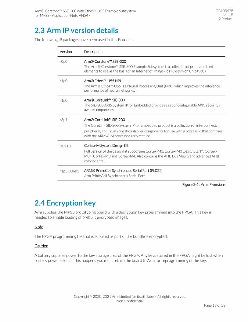
2.3 Arm IP version details The following IP packages have been used in this Product.
Version Description
r0p0 Arm® Corstone™ SSE-300
The Arm® Corstone™ SSE-300 Example Subsystem is a collection of pre-assembled elements to use as the basis of an Internet of Things (IoT) System on Chip (SoC).
r1p0 Arm® Ethos™-U55 NPU
The Arm® Ethos™-U55 is a Neural Processing Unit (NPU) which improves the inference performance of neural networks.
r1p0 Arm® CoreLink™ SIE-300
The SIE-300 AXI5 System IP for Embedded provides a set of configurable AXI5 security-aware components.
r3p1 Arm® CoreLink™ SIE-200
The CoreLink SIE-200 System IP for Embedded product is a collection of interconnect,
peripheral, and TrustZone® controller components for use with a processor that complies
with the ARMv8-M processor architecture.
BP210 Cortex-M System Design Kit
Full version of the design kit supporting Cortex-M0, Cortex-M0 DesignStart®, Cortex-
M0+, Cortex-M3 and Cortex-M4. Also contains the AHB Bus Matrix and advanced AHB
components.
r1p3-00rel1 ARM® PrimeCell Synchronous Serial Port (PL022)
Arm PrimeCell Synchronous Serial Port
Figure 2-1 : Arm IP versions
2.4 Encryption key Arm supplies the MPS3 prototyping board with a decryption key programmed into the FPGA. This key is
needed to enable loading of prebuilt encrypted images.
Note
The FPGA programming file that is supplied as part of the bundle is encrypted.
Caution
A battery supplies power to the key storage area of the FPGA. Any keys stored in the FPGA might be lost when
battery power is lost. If this happens you must return the board to Arm for reprogramming of the key.
Arm® Corstone™ SSE-300 with Ethos™-U55 Example Subsystem for MPS3 - Application Note AN547
DAI 0547B Issue B
3 Overview
Copyright © 2020, 2021 Arm Limited (or its affiliates). All rights reserved. Non-Confidential
Page 14 of 53
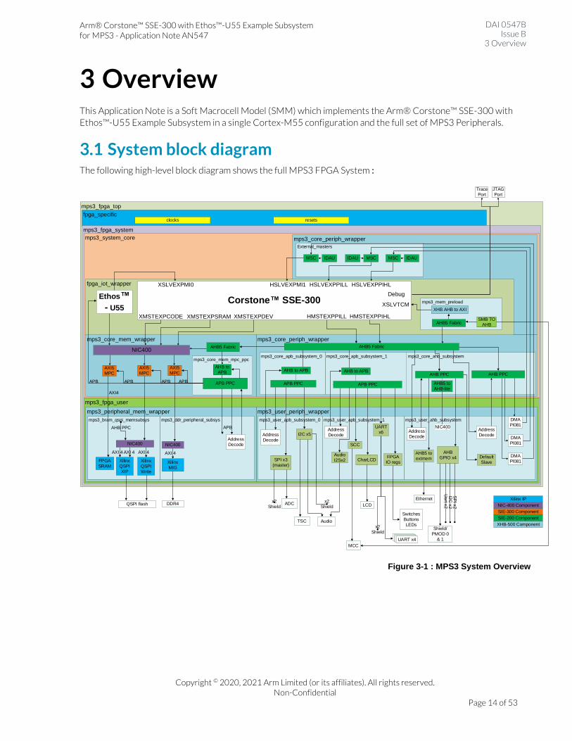
3 Overview This Application Note is a Soft Macrocell Model (SMM) which implements the Arm® Corstone™ SSE-300 with
Ethos™-U55 Example Subsystem in a single Cortex-M55 configuration and the full set of MPS3 Peripherals.
3.1 System block diagram The following high-level block diagram shows the full MPS3 FPGA System :
mps3_fpga_top
fpga_specific
mps3_fpga_system
mps3_fpga_user
mps3_user_periph_wrapper
mps3_user_ahb_subsystemmps3_user_apb_subsystem_1mps3_user_apb_subsystem_0
mps3_peripheral_mem_wrapper
mps3_ddr_peripheral_subsys
mps3_system_core mps3_core_periph_wrapper
fpga_iot_wrapper
mps3_mem_preload
mps3_core_periph_wrapper
mps3_core_ahb_subsystemmps3_core_apb_subsystem_1mps3_core_apb_subsystem_0
mps3_core_mem_wrapper
mps3_core_mem_mpc_ppc
Trace
Port
JTAG
Port
Ethernet
LCD
Shield/
PMOD 0
& 1
TSC Audio
Switches
Buttons
LEDs
ADCQSPI flash
MCC
DDR4
AXI5
MPC
AHB to
APB
APB PPC APB PPC
AHB to APBAHB PPC
AXI5
MPC
APBAPB AHB5 to
AHB-lite
NIC400
AXI5
MPC
APB
APB
SMB TO
AHB
clocks resets
mps3_bram_qspi_memsubsys
Default
Slave
AHB
GPIO x4
UART
x6
SPI x3
(master)
Audio
I2Sx2FPGA
IO regsCharLCD
SCC
I2C x5
x2
Shield
NIC400
Xilinx
QSPI
XIP
x2
Shield
x2
Shield
Ua
rt x2
SP
I x2
I2C
x2
Xilinx
QSPI
Write
AXI 4AXI 4 AXI 4
AXI4
AHB5 to
extmem
Address
DecodeAddress
Decode
Address
Decode
Address
Decode
AXI 4
NIC400
AHB PPC
FPGA
SRAMXilinx
MIG
Corstone SSE-300
DMA
Pl081
AHB PPC
SIE-300 Component
SIE-200 Component
XHB-500 Component
NIC-400 Component
Xilinx IP
XHB AHB to AXI
NIC400
DMA
Pl081
DMA
Pl081
Address
Decode
External_masters
MSC
Ethos
- U55
IDAU MSCMSC IDAUIDAU
AHB5 Fabric
APB
AHB5 Fabric
XSLVEXPMI0 HSLVEXPMI1 HSLVEXPPILL HSLVEXPPIHL
XMSTEXPCODE XMSTEXPSRAM XMSTEXPDEV HMSTEXPPILL HMSTEXPPIHL
Debug
XSLVTCM
UARTUARTUARTUART x4
APB PPC
AHB5 Fabric
AHB to APB
Figure 3-1 : MPS3 System Overview
Arm® Corstone™ SSE-300 with Ethos™-U55 Example Subsystem for MPS3 - Application Note AN547
DAI 0547B Issue B
3 Overview
Copyright © 2020, 2021 Arm Limited (or its affiliates). All rights reserved. Non-Confidential
Page 15 of 53
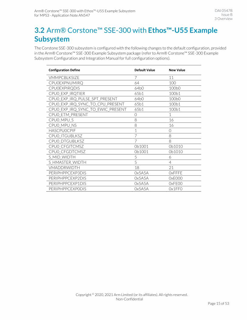
3.2 Arm® Corstone™ SSE-300 with Ethos™-U55 Example Subsystem The Corstone SSE-300 subsystem is configured with the following changes to the default configuration, provided
in the Arm® Corstone™ SSE-300 Example Subsystem package (refer to Arm® Corstone™ SSE-300 Example
Subsystem Configuration and Integration Manual for full configuration options).
Configuration Define Default Value New Value
VMMPCBLKSIZE 7 11
CPU0EXPNUMIRQ 64 100
CPU0EXPIRQDIS 64b0 100b0
CPU0_EXP_IRQTIER 65b1 100b1
CPU0_EXP_IRQ_PULSE_SPT_PRESENT 64b0 100b0
CPU0_EXP_IRQ_SYNC_TO_CPU_PRESENT 65b1 100b1
CPU0_EXP_IRQ_SYNC_TO_EWIC_PRESENT 65b1 100b1
CPU0_ETM_PRESENT 0 1
CPU0_MPU_S 8 16
CPU0_MPU_NS 8 16
HASCPU0CPIF 1 0
CPU0_ITGUBLKSZ 7 8
CPU0_DTGUBLKSZ 7 8
CPU0_CFGITCMSZ 0b1001 0b1010
CPU0_CFGDTCMSZ 0b1001 0b1010
S_MID_WIDTH 5 6
S_HMASTER_WIDTH 5 4
VMADDRWIDTH 18 21
PERIPHPPCEXP3DIS 0x5A5A 0xFFFE
PERIPHPPCEXP2DIS 0x5A5A 0xE000
PERIPHPPCEXP1DIS 0x5A5A 0xFE00
PERIPHPPCEXP0DIS 0x5A5A 0x1FF0
Arm® Corstone™ SSE-300 with Ethos™-U55 Example Subsystem for MPS3 - Application Note AN547
DAI 0547B Issue B
3 Overview
Copyright © 2020, 2021 Arm Limited (or its affiliates). All rights reserved. Non-Confidential
Page 16 of 53
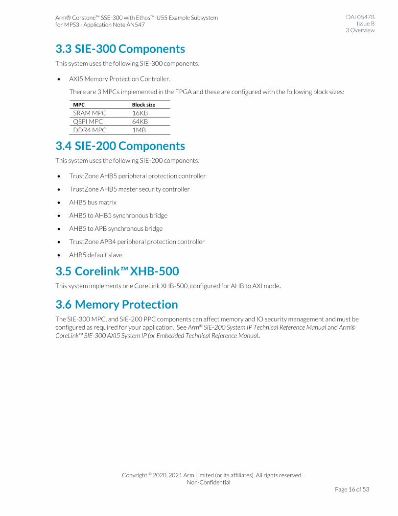
3.3 SIE-300 Components This system uses the following SIE-300 components:
• AXI5 Memory Protection Controller.
There are 3 MPCs implemented in the FPGA and these are configured with the following block sizes:
MPC Block size
SRAM MPC 16KB
QSPI MPC 64KB
DDR4 MPC 1MB
3.4 SIE-200 Components This system uses the following SIE-200 components:
• TrustZone AHB5 peripheral protection controller
• TrustZone AHB5 master security controller
• AHB5 bus matrix
• AHB5 to AHB5 synchronous bridge
• AHB5 to APB synchronous bridge
• TrustZone APB4 peripheral protection controller
• AHB5 default slave
3.5 Corelink™ XHB-500 This system implements one CoreLink XHB-500, configured for AHB to AXI mode.
3.6 Memory Protection The SIE-300 MPC, and SIE-200 PPC components can affect memory and IO security management and must be
configured as required for your application. See Arm® SIE-200 System IP Technical Reference Manual and Arm®
CoreLink™ SIE-300 AXI5 System IP for Embedded Technical Reference Manual.
Arm® Corstone™ SSE-300 with Ethos™-U55 Example Subsystem for MPS3 - Application Note AN547
DAI 0547B Issue B
3 Overview
Copyright © 2020, 2021 Arm Limited (or its affiliates). All rights reserved. Non-Confidential
Page 17 of 53
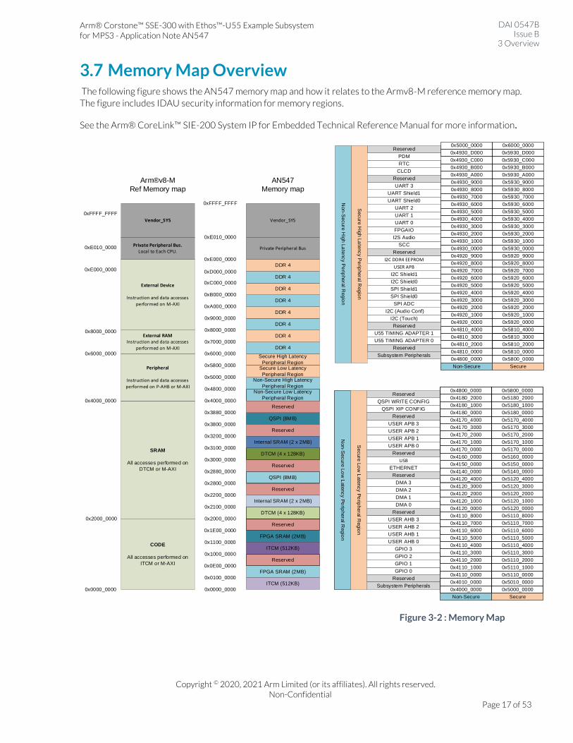
3.7 Memory Map Overview The following figure shows the AN547 memory map and how it relates to the Armv8-M reference memory map.
The figure includes IDAU security information for memory regions.
See the Arm® CoreLink™ SIE-200 System IP for Embedded Technical Reference Manual for more information.
SRAM
All accesses performed on
DTCM or M-AXI
CODE
All accesses performed on
ITCM or M-AXI
Peripheral
Instruction and data accesses
performed on P-AHB or M-AXI
External RAMInstruction and data accesses
performed on M-AXI
External Device
Instruction and data accesses
performed on M-AXI
Private Peripheral Bus.Local to Each CPU.
Vendor_SYS
0x0000_0000
0x2000_0000
0x4000_0000
0xE000_0000
0xE010_0000
0xFFFF_FFFF
0x6000_0000
0x8000_0000
0x5000_0000
QSPI (8MB)
0x2000_0000
0x2200_0000
Reserved
0x2800_0000
DTCM (4 x 128KB)
Reserved
FPGA SRAM (2MB)
0x3000_0000
Non-Secure Low Latency
Peripheral Region
Non-Secure High Latency
Peripheral Region0x4800_0000
Secure High Latency
Peripheral Region0x5800_0000
Private Peripheral Bus
Vendor_SYS
0xFFFF_FFFF
0xE010_0000
GPIO 00x4110_1000
GPIO 10x4110_2000
GPIO 20x4110_3000
GPIO 30x4110_4000
Reserved
I2C (Touch)
I2C (Audio Conf)
SPI ADC
SPI Shield0
SPI Shield1
I2C Shield0
I2C Shield1
Reserved
SCC
I2S Audio
FPGAIO
UART 0
UART 1
UART 2
UART Shield0
UART Shield1
UART 3
CLCD
Reserved
ETHERNET
QSPI XIP CONFIG
QSPI WRITE CONFIG
Reserved
RTC
0x4110_0000
0x4800_0000
0x4810_0000
0x4920_0000
0x4140_0000
0x4160_0000
0x4150_0000USB
0x9000_0000
0xA000_0000
0xB000_0000
0xC000_0000
0xD000_0000
0x6000_0000DDR 4
DDR 40x7000_0000
0x8000_0000
0xE000_0000
DDR 4
DDR 4
DDR 4
DDR 4
DDR 4
DDR 4
0x1E00_0000
0x0000_0000
Reserved
FPGA SRAM (2MB)
ITCM (512KB)
I2C DDR4 EEPROM
Reserved
Reserved
Arm®v8-M
Ref Memory map
AN547
Memory map
0x0100_0000
QSPI (8MB)
Reserved
ITCM (512KB)
0x2100_0000
0x2880_0000
DTCM (4 x 128KB)
Reserved
Reserved
Secure Low Latency
Peripheral Region
Reserved
Subsystem Peripherals0x4010_0000
0x4000_0000
USER AHB 00x4110_5000
USER AHB 10x4110_6000
USER AHB 20x4110_7000
USER AHB 30x4110_8000
0x4120_0000DMA 0
0x4120_1000DMA 1
0x4120_2000DMA 2
0x4120_3000DMA 3
0x4120_4000Reserved
USER APB 0
USER APB 1
USER APB 2
USER APB 3
0x4170_1000
0x4170_2000
0x4170_3000
0x4170_4000
0x4170_0000
Reserved0x4180_0000
0x4180_2000
0x4180_1000
0x4800_0000
0x5110_1000
0x5110_2000
0x5110_3000
0x5110_4000
0x5110_0000
0x5140_0000
0x5160_0000
0x5150_0000
0x5010_0000
0x5000_0000
0x5110_5000
0x5110_6000
0x5110_7000
0x5110_8000
0x5120_0000
0x5120_1000
0x5120_2000
0x5120_3000
0x5120_4000
0x5170_1000
0x5170_2000
0x5170_3000
0x5170_4000
0x5170_0000
0x5180_0000
0x5180_2000
0x5180_1000
0x5800_0000
Reserved
Non
-Secure
Lo
w L
ate
ncy P
erip
hera
l Regio
n
Secure
Lo
w L
ate
ncy P
erip
hera
l Regio
nS
ecure
Hig
h L
ate
ncy P
erip
hera
l Regio
n
Non
-Secure
Hig
h L
ate
ncy P
erip
hera
l Regio
n
Subsystem Peripherals
USER APB
0x4920_1000
0x4920_2000
0x4920_3000
0x4920_4000
0x4920_5000
0x4920_6000
0x4920_7000
0x4920_8000
0x4920_9000
0x4930_0000
0x4930_1000
0x4930_2000
0x4930_3000
0x4930_4000
0x4930_5000
0x4930_6000
0x4930_7000
0x4930_8000
0x4930_9000
0x4930_A000
0x4930_B000
0x4930_C000
0x5000_0000
0x5800_0000
0x5810_0000
0x5920_0000
0x5920_1000
0x5920_2000
0x5920_3000
0x5920_4000
0x5920_5000
0x5920_6000
0x5920_7000
0x5920_8000
0x5920_9000
0x5930_0000
0x5930_1000
0x5930_2000
0x5930_3000
0x5930_4000
0x5930_5000
0x5930_6000
0x5930_7000
0x5930_8000
0x5930_9000
0x5930_A000
0x5930_B000
0x5930_C000
0x6000_0000
Internal SRAM (2 x 2MB)
Internal SRAM (2 x 2MB)
0x0E00_0000
0x1000_0000
0x1100_0000
0x3200_0000
0x3800_0000
0x4000_0000
0x3100_0000
0x3880_0000
Non-Secure Secure
Non-Secure Secure
PDM0x4930_D000 0x5930_D000
0x4810_2000U55 TIMING ADAPTER 0
U55 TIMING ADAPTER 1
Reserved
0x4810_3000
0x4810_4000
0x5810_2000
0x5810_3000
0x5810_4000
Figure 3-2 : Memory Map
Arm® Corstone™ SSE-300 with Ethos™-U55 Example Subsystem for MPS3 - Application Note AN547
DAI 0547B Issue B
3 Overview
Copyright © 2020, 2021 Arm Limited (or its affiliates). All rights reserved. Non-Confidential
Page 18 of 53
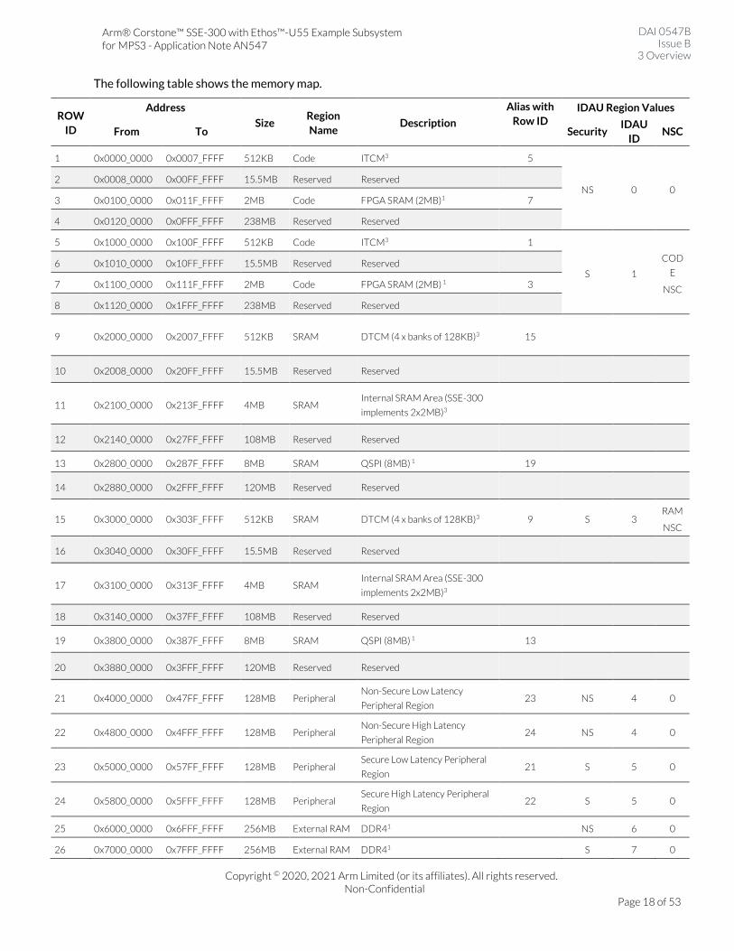
The following table shows the memory map.
ROW
ID
Address
Size Region
Name Description
Alias with
Row ID IDAU Region Values
From To Security IDAU
ID NSC
1 0x0000_0000 0x0007_FFFF 512KB Code ITCM3 5
NS 0 0 2 0x0008_0000 0x00FF_FFFF 15.5MB Reserved Reserved
3 0x0100_0000 0x011F_FFFF 2MB Code FPGA SRAM (2MB)1 7
4 0x0120_0000 0x0FFF_FFFF 238MB Reserved Reserved
5 0x1000_0000 0x100F_FFFF 512KB Code ITCM3 1
S 1
COD
E
NSC
6 0x1010_0000 0x10FF_FFFF 15.5MB Reserved Reserved
7 0x1100_0000 0x111F_FFFF 2MB Code FPGA SRAM (2MB) 1 3
8 0x1120_0000 0x1FFF_FFFF 238MB Reserved Reserved
9 0x2000_0000 0x2007_FFFF 512KB SRAM DTCM (4 x banks of 128KB)3 15 N
S 2 0
10 0x2008_0000 0x20FF_FFFF 15.5MB Reserved Reserved
11 0x2100_0000 0x213F_FFFF 4MB SRAM Internal SRAM Area (SSE-300
implements 2x2MB)3
1
7
12 0x2140_0000 0x27FF_FFFF 108MB Reserved Reserved
13 0x2800_0000 0x287F_FFFF 8MB SRAM QSPI (8MB) 1 19
14 0x2880_0000 0x2FFF_FFFF 120MB Reserved Reserved
15 0x3000_0000 0x303F_FFFF 512KB SRAM DTCM (4 x banks of 128KB)3 9 S 3 RAM
NSC
16 0x3040_0000 0x30FF_FFFF 15.5MB Reserved Reserved
17 0x3100_0000 0x313F_FFFF 4MB SRAM Internal SRAM Area (SSE-300
implements 2x2MB)3
1
1
18 0x3140_0000 0x37FF_FFFF 108MB Reserved Reserved
19 0x3800_0000 0x387F_FFFF 8MB SRAM QSPI (8MB) 1 13
20 0x3880_0000 0x3FFF_FFFF 120MB Reserved Reserved
21 0x4000_0000 0x47FF_FFFF 128MB Peripheral Non-Secure Low Latency
Peripheral Region 23 NS 4 0
22 0x4800_0000 0x4FFF_FFFF 128MB Peripheral Non-Secure High Latency
Peripheral Region 24 NS 4 0
23 0x5000_0000 0x57FF_FFFF 128MB Peripheral Secure Low Latency Peripheral
Region 21 S 5 0
24 0x5800_0000 0x5FFF_FFFF 128MB Peripheral Secure High Latency Peripheral
Region 22 S 5 0
25 0x6000_0000 0x6FFF_FFFF 256MB External RAM DDR41 NS 6 0
26 0x7000_0000 0x7FFF_FFFF 256MB External RAM DDR41 S 7 0
Arm® Corstone™ SSE-300 with Ethos™-U55 Example Subsystem for MPS3 - Application Note AN547
DAI 0547B Issue B
3 Overview
Copyright © 2020, 2021 Arm Limited (or its affiliates). All rights reserved. Non-Confidential
Page 19 of 53
ROW
ID
Address
Size Region
Name Description
Alias with
Row ID IDAU Region Values
From To Security IDAU
ID NSC
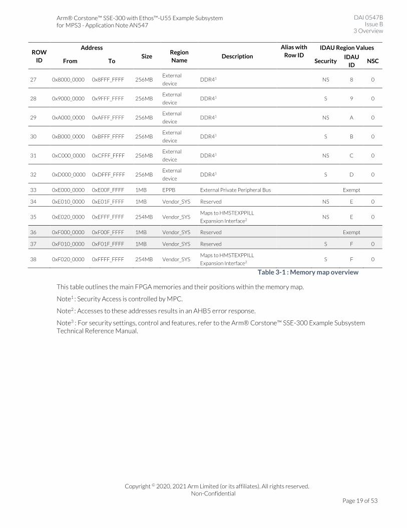
27 0x8000_0000 0x8FFF_FFFF 256MB External
device DDR41 NS 8 0
28 0x9000_0000 0x9FFF_FFFF 256MB External
device DDR41 S 9 0
29 0xA000_0000 0xAFFF_FFFF 256MB External
device DDR41 NS A 0
30 0xB000_0000 0xBFFF_FFFF 256MB External
device DDR41 S B 0
31 0xC000_0000 0xCFFF_FFFF 256MB External
device DDR41 NS C 0
32 0xD000_0000 0xDFFF_FFFF 256MB External
device DDR41 S D 0
33 0xE000_0000 0xE00F_FFFF 1MB EPPB External Private Peripheral Bus Exempt
34 0xE010_0000 0xE01F_FFFF 1MB Vendor_SYS Reserved NS E 0
35 0xE020_0000 0xEFFF_FFFF 254MB Vendor_SYS Maps to HMSTEXPPILL
Expansion Interface2 NS E 0
36 0xF000_0000 0xF00F_FFFF 1MB Vendor_SYS Reserved Exempt
37 0xF010_0000 0xF01F_FFFF 1MB Vendor_SYS Reserved S F 0
38 0xF020_0000 0xFFFF_FFFF 254MB Vendor_SYS Maps to HMSTEXPPILL
Expansion Interface2 S F 0
Table 3-1 : Memory map overview
This table outlines the main FPGA memories and their positions within the memory map.
Note1 : Security Access is controlled by MPC.
Note2 : Accesses to these addresses results in an AHB5 error response.
Note3 : For security settings, control and features, refer to the Arm® Corstone™ SSE-300 Example Subsystem Technical Reference Manual.
Arm® Corstone™ SSE-300 with Ethos™-U55 Example Subsystem for MPS3 - Application Note AN547
DAI 0547B Issue B
3 Overview
Copyright © 2020, 2021 Arm Limited (or its affiliates). All rights reserved. Non-Confidential
Page 20 of 53
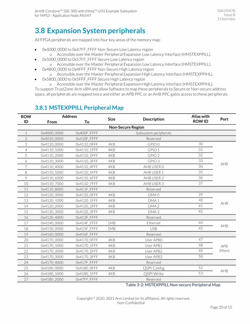
3.8 Expansion System peripherals All FPGA peripherals are mapped into four key areas of the memory map:
• 0x4000_0000 to 0x47FF_FFFF Non-Secure Low Latency region o Accessible over the Master Peripheral Expansion Low Latency Interface (HMSTEXPPILL).
• 0x5000_0000 to 0x57FF_FFFF Secure Low Latency region o Accessible over the Master Peripheral Expansion Low Latency Interface (HMSTEXPPILL).
• 0x4800_0000 to 0x4FFF_FFFF Non-Secure High Latency region o Accessible over the Master Peripheral Expansion High Latency Interface (HMSTEXPPIHL).
• 0x5800_0000 to 0x5FFF_FFFF Secure High Latency region o Accessible over the Master Peripheral Expansion High Latency Interface (HMSTEXPPIHL).
To support TrustZone-Arm v8M and allow Software to map these peripherals to Secure or Non-secure address
space, all peripherals are mapped twice and either an APB PPC or an AHB PPC gates access to these peripherals.
3.8.1 MSTEXPPILL Peripheral Map
ROW ID
Address Size Description
Alias with ROW ID
Port From To
Non-Secure Region
1 0x4000_0000 0x400F_FFFF Subsystem peripherals
2 0x4010_0000 0x410F_FFFF Reserved
3 0x4110_0000 0x4110_0FFF 4KB GPIO 0 30
AHB
4 0x4110_1000 0x4110_1FFF 4KB GPIO 1 31
5 0x4110_2000 0x4110_2FFF 4KB GPIO 2 32
6 0x4110_3000 0x4110_3FFF 4KB GPIO 3 33
7 0x4110_4000 0x4110_4FFF 4KB AHB USER 0 34
8 0x4110_5000 0x4110_5FFF 4KB AHB USER 1 35
9 0x4110_6000 0x4110_6FFF 4KB AHB USER 2 36
10 0x4110_7000 0x4110_7FFF 4KB AHB USER 3 37
11 0x4110_8000 0x411F_FFFF Reserved
12 0x4120_0000 0x4120_0FFF 4KB DMA 0 39
AHB 13 0x4120_1000 0x4120_1FFF 4KB DMA 1 40
14 0x4120_2000 0x4120_2FFF 4KB DMA 2 41
15 0x4120_3000 0x4120_3FFF 4KB DMA 3 42
16 0x4120_4000 0x413F_FFFF Reserved
17 0x4140_0000 0x414F_FFFF 1MB Ethernet 44 AHB
18 0x4150_0000 0x415F_FFFF 1MB USB 45
19 0x4160_0000 0x416F_FFFF Reserved
20 0x4170_0000 0x4170_0FFF 4KB User APB0 47
APB (Mem)
21 0x4170_1000 0x4170_1FFF 4KB User APB1 48
22 0x4170_2000 0x4170_2FFF 4KB User APB2 49
23 0x4170_3000 0x4170_3FFF 4KB User APB3 50
24 0x4170_4000 0x417F_FFFF Reserved
25 0x4180_0000 0x4180_0FFF 4KB QSPI Config 52 AHB
26 0x4180_1000 0x4180_1FFF 4KB QSPI Write 53
27 0x4180_2000 0x47FF_FFFF Reserved
Table 3-2: MSTEXPPILL Non-secure Peripheral Map
Arm® Corstone™ SSE-300 with Ethos™-U55 Example Subsystem for MPS3 - Application Note AN547
DAI 0547B Issue B
3 Overview
Copyright © 2020, 2021 Arm Limited (or its affiliates). All rights reserved. Non-Confidential
Page 21 of 53
ROW ID
Address Size Description
Alias with ROW ID
Port From To
Secure Region
28 0x5000_0000 0x500F_FFFF Subsystem peripherals
29 0x5010_0000 0x510F_FFFF Reserved
30 0x5110_0000 0x5110_0FFF 4KB GPIO 0 3
AHB
31 0x5110_1000 0x5110_1FFF 4KB GPIO 1 4
32 0x5110_2000 0x5110_2FFF 4KB GPIO 2 5
33 0x5110_3000 0x5110_3FFF 4KB GPIO 3 6
34 0x5110_4000 0x5110_4FFF 4KB AHB USER 0 7
35 0x5110_5000 0x5110_5FFF 4KB AHB USER 1 8
36 0x5110_6000 0x5110_6FFF 4KB AHB USER 2 9
37 0x5110_7000 0x5110_7FFF 4KB AHB USER 3 10
38 0x5110_8000 0x511F_FFFF Reserved
39 0x5120_0000 0x5120_0FFF 4KB DMA 0 12
AHB 40 0x5120_1000 0x5120_1FFF 4KB DMA 1 13
41 0x5120_2000 0x5120_2FFF 4KB DMA 2 14
42 0x5120_3000 0x5120_3FFF 4KB DMA 3 15
43 0x5120_4000 0x513F_FFFF Reserved
44 0x5140_0000 0x514F_FFFF 1M Ethernet 17 AHB
45 0x5150_0000 0x515F_FFFF 1M USB 18
46 0x5160_0000 0x516F_FFFF Reserved
47 0x5170_0000 0x5170_0FFF 4KB User APB0 20
APB (Mem)
48 0x5170_1000 0x5170_1FFF 4KB User APB1 21
49 0x5170_2000 0x5170_2FFF 4KB User APB2 22
50 0x5170_3000 0x5170_3FFF 4KB User APB3 23
51 0x5170_4000 0x517F_FFFF Reserved
52 0x5180_0000 0x5180_0FFF 4KB QSPI Config 25 AHB
53 0x5180_1000 0x5180_1FFF 4KB QSPI Write 26
54 0x5180_2000 0x56FF_FFFF Reserved
55 0x5700_0000 0x5700_0FFF 4KB SRAM Memory Protection Controller
(MPC)
APB (Mem)
56 0x5700_1000 0x5700_1FFF 4KB QSPI Memory Protection Controller
(MPC)
57 0x5700_2000 0x5700_2FFF 4KB DDR4 Memory Protection Controller
(MPC)
58 0x5700_3000 0x57FF_FFFF Reserved
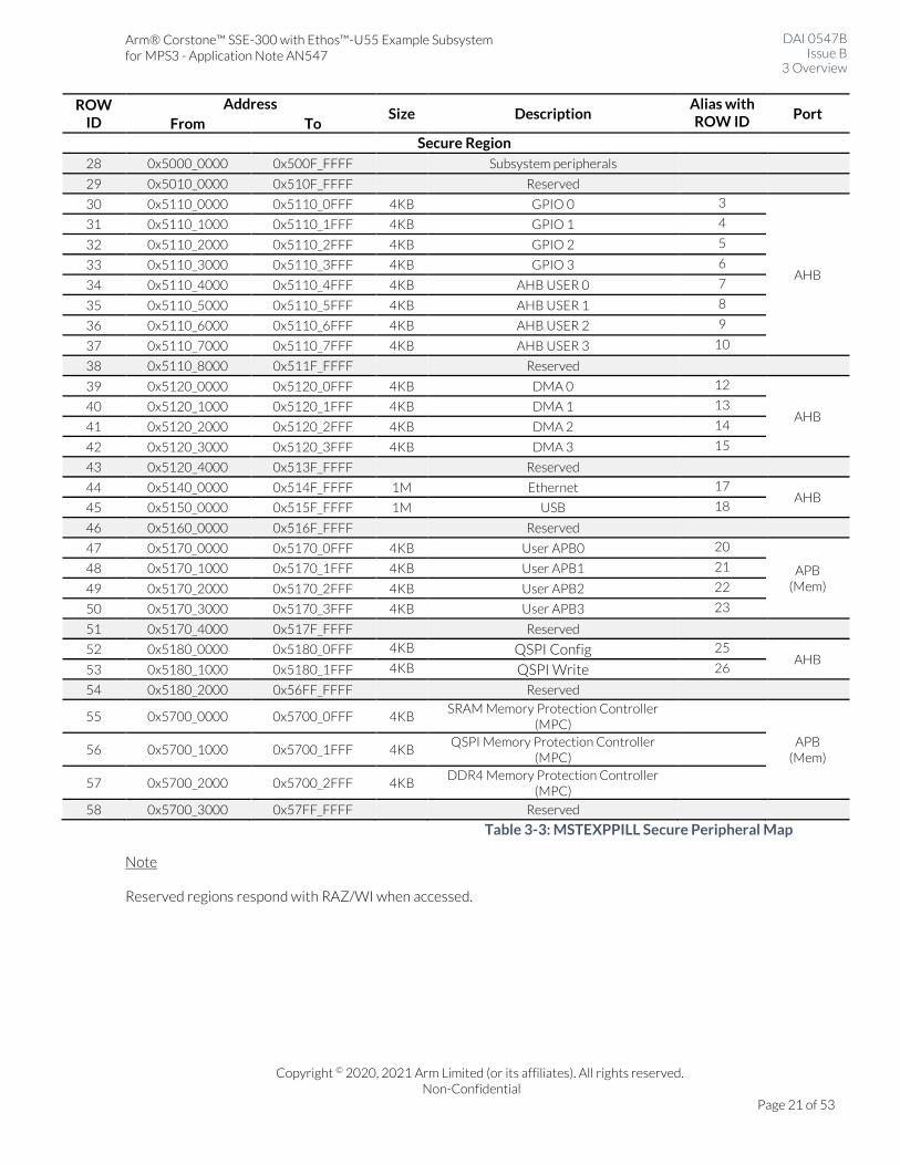
Table 3-3: MSTEXPPILL Secure Peripheral Map
Note
Reserved regions respond with RAZ/WI when accessed.
Arm® Corstone™ SSE-300 with Ethos™-U55 Example Subsystem for MPS3 - Application Note AN547
DAI 0547B Issue B
3 Overview
Copyright © 2020, 2021 Arm Limited (or its affiliates). All rights reserved. Non-Confidential
Page 22 of 53
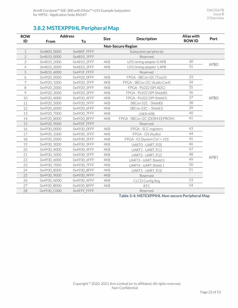
3.8.2 MSTEXPPIHL Peripheral Map
ROW ID
Address Size Description
Alias with ROW ID
Port From To
Non-Secure Region
1 0x4800_0000 0x480F_FFFF Subsystem peripherals
2 0x4810_0000 0x4810_1FFF Reserved
3 0x4810_2000 0x4810_2FFF 4KB U55 timing adapter 0 APB 30 APB0
4 0x4810_3000 0x4810_3FFF 4KB U55 timing adapter 1 APB 31
5 0x4810_4000 0x491F_FFFF Reserved
6 0x4920_0000 0x4920_0FFF 4KB FPGA - SBCon I2C (Touch) 33
APB0
7 0x4920_1000 0x4920_1FFF 4KB FPGA - SBCon I2C (Audio Conf) 34
8 0x4920_2000 0x4920_2FFF 4KB FPGA - PL022 (SPI ADC) 35
9 0x4920_3000 0x4920_3FFF 4KB FPGA - PL022 (SPI Shield0) 36
10 0x4920_4000 0x4920_4FFF 4KB FPGA - PL022 (SPI Shield1) 37
11 0x4920_5000 0x4920_5FFF 4KB SBCon (I2C - Shield0) 38
12 0x4920_6000 0x4920_6FFF 4KB SBCon (I2C – Shield1) 39
13 0x4920_7000 0x4920_7FFF 4KB USER APB 40
14 0x4920_8000 0x4920_8FFF 4KB FPGA - SBCon I2C (DDR4 EEPROM) 41
15 0x4920_9000 0x492F_FFFF Reserved
16 0x4930_0000 0x4930_0FFF 4KB FPGA - SCC registers 43
APB1
17 0x4930_1000 0x4930_1FFF 4KB FPGA - I2S (Audio) 44
18 0x4930_2000 0x4930_2FFF 4KB FPGA - IO (System Ctrl + I/O) 45
19 0x4930_3000 0x4930_3FFF 4KB UART0 - UART_F[0] 46
20 0x4930_4000 0x4930_4FFF 4KB UART1 - UART_F[1] 47
21 0x4930_5000 0x4930_5FFF 4KB UART2 - UART_F[2] 48
22 0x4930_6000 0x4930_6FFF 4KB UART3 - UART Shield 0 49
23 0x4930_7000 0x4930_7FFF 4KB UART4 - UART Shield 1 50
24 0x4930_8000 0x4930_8FFF 4KB UART5 - UART_F[3] 51
25 0x4930_9000 0x4930_9FFF 4KB Reserved
26 0x4930_A000 0x4930_AFFF 4KB CLCD Config Reg 53
27 0x4930_B000 0x4930_BFFF 4KB RTC 54
28 0x4930_C000 0x4FFF_FFFF Reserved
Table 3-4: MSTEXPPIHL Non-secure Peripheral Map
Arm® Corstone™ SSE-300 with Ethos™-U55 Example Subsystem for MPS3 - Application Note AN547
DAI 0547B Issue B
3 Overview
Copyright © 2020, 2021 Arm Limited (or its affiliates). All rights reserved. Non-Confidential
Page 23 of 53
ROW ID
Address Size Description
Alias with ROW ID
Port From To
Secure Region
29 0x5800_0000 0x5810_1FFF Subsystem peripherals
30 0x5810_2000 0x5810_2FFF 4KB U55 timing adapter 0 APB 3 APB0
31 0x5810_3000 0x5810_3FFF 4KB U55 timing adapter 1 APB 4
32 0x5810_4000 0x591F_FFFF Reserved
33 0x5920_0000 0x5920_0FFF 4KB FPGA - SBCon I2C (Touch) 6
APB0
34 0x5920_1000 0x5920_1FFF 4KB FPGA - SBCon I2C (Audio Conf) 7
35 0x5920_2000 0x5920_2FFF 4KB FPGA - PL022 (SPI ADC) 8
36 0x5920_3000 0x5920_3FFF 4KB FPGA - PL022 (SPI Shield0) 9
37 0x5920_4000 0x5920_4FFF 4KB FPGA - PL022 (SPI Shield1) 10
38 0x5920_5000 0x5920_5FFF 4KB SBCon (I2C - Shield0) 11
39 0x5920_6000 0x5920_6FFF 4KB SBCon (I2C - Shield1) 12
40 0x5920_7000 0x5920_7FFF 4KB USER APB 13
41 0x5920_8000 0x5920_8FFF 4KB FPGA - SBCon I2C (DDR4 EEPROM) 14
42 0x5920_9000 0x592F_FFFF Reserved
43 0x5930_0000 0x5930_0FFF 4KB FPGA - SCC registers 16
APB1
44 0x5930_1000 0x5930_1FFF 4KB FPGA - I2S (Audio) 17
45 0x5930_2000 0x5930_2FFF 4KB FPGA - IO (System Ctrl + I/O) 18
46 0x5930_3000 0x5930_3FFF 4KB UART0 - UART_F[0] 19
47 0x5930_4000 0x5930_4FFF 4KB UART1 - UART_F[1] 20
48 0x5930_5000 0x5930_5FFF 4KB UART2 - UART_F[2] 21
49 0x5930_6000 0x5930_6FFF 4KB UART3 - UART Shield 0 22
50 0x5930_7000 0x5930_7FFF 4KB UART4 - UART Shield 1 23
51 0x5930_8000 0x5930_8FFF 4KB UART5 - UART_F[3] 24
52 0x5930_9000 0x5930_9FFF 4KB Reserved
53 0x5930_A000 0x5930_AFFF 4KB CLCD Config Reg 26
54 0x5930_B000 0x5930_BFFF 4KB RTC 27
55 0x5930_C000 0x5FFF_FFFF Reserved
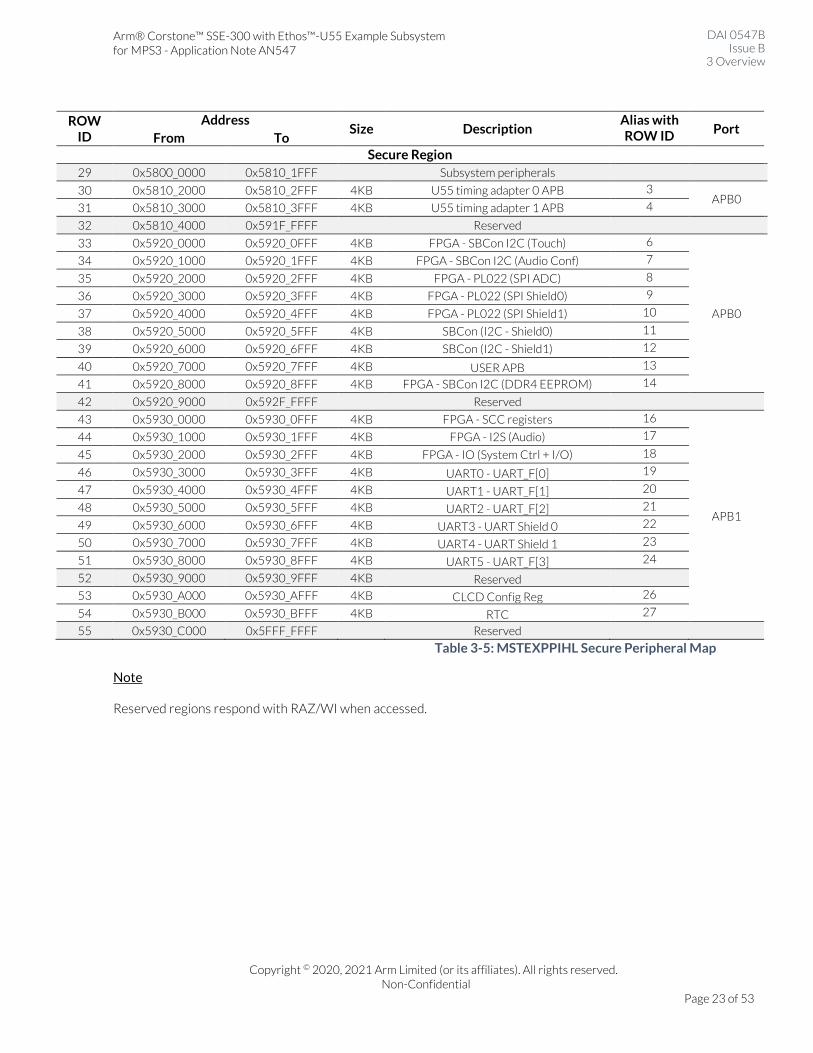
Table 3-5: MSTEXPPIHL Secure Peripheral Map
Note
Reserved regions respond with RAZ/WI when accessed.
Arm® Corstone™ SSE-300 with Ethos™-U55 Example Subsystem for MPS3 - Application Note AN547
DAI 0547B Issue B
4 Programmers Model
Copyright © 2020, 2021 Arm Limited (or its affiliates). All rights reserved. Non-Confidential
Page 24 of 53
4 Programmers Model This programmers model is supplemental to the CMSDK (DDI 0479), SIE-200 (DDI 0571) and SIE-300 (101526)
documentation which covers many of the included components in more detail. The connectivity of the system is
shown in MPS3 System Overview Diagram.
4.1 ITCM The primary boot memory is an ITCM which is implemented with 512KB of FPGA SRAM connected to the ITCM
interface of the Cortex-M55 inside the subsystem.
• Size: 512KB FPGA SRAM
• Address Range: 0x0000_0000 - 0x0007_FFFF
• Alias Range: 0x1000_0000 - 0x1007_FFFF
4.2 FPGA SRAM The code memory is extended with 2MB of internal FPGA SRAM.
• Size: 2MB FPGA SRAM
• Address Range: 0x0100_0000 - 0x011F_FFFF
• Alias Range: 0x1100_0000 - 0x111F_FFFF
4.3 DTCM The primary data memory is provided by DTCM made up of 4 banks, each implemented as 128KB of internal
FPGA SRAM connected to the 4 DTCM interfaces of the Cortex-M55 inside the subsystem.
• Size: 4 x 128KB FPGA SRAM
• Address Range: 0x2000_0000 - 0x2007_FFFF
• Alias Range: 0x3000_0000 - 0x3007_FFFF
4.4 QSPI The SMM provides 8MB of external Flash memory which is accessed through a QSPI interface.
• Size: 8MB fitted
• Address Range: 0x2800_0000 - 0x287F_FFFF
• Alias Range: 0x3800_0000 - 0x387F_FFFF
4.5 DDR4 The SMM provides access to 2GB of External DDR4 memory via DDR4 controller.
• Size: 2GB DDR4 (4GB fitted only 2GB accessible)
• Address Range: 0x6000_0000 - 0xDFFF_FFFF
Arm® Corstone™ SSE-300 with Ethos™-U55 Example Subsystem for MPS3 - Application Note AN547
DAI 0547B Issue B
4 Programmers Model
Copyright © 2020, 2021 Arm Limited (or its affiliates). All rights reserved. Non-Confidential
Page 25 of 53
4.6 AHB GPIO The SMM uses four CMSDK AHB GPIO blocks, each providing 16 bits of IO. These are connected to the two
Arduino compatible headers shield 0 and 1 as follows:
Shield GPIO
SH0_IO [15:0] GPIO0[15:0]
SH0_IO [17:16] GPIO2[1:0]
SH1_IO [15:0] GPIO1[15:0]
SH1_IO [17:16] GPIO2[3:2]
Table 4-1 : GPIO Mapping
The GPIO alternative function lines select whether peripherals or GPIOs are available on each pin. See Shield
Support Section for mappings.
4.7 SPI The SMM implements three PL022 SPI modules:
• One general purpose SPI module (SPI ADC) is used for communication with an onboard ADC. The analog pins of the Shield headers are connected to the input channels of the ADC.
• Two general purpose SPI modules connect to the Shield headers and provide an SPI interface on each header. These are alt-functions on the GPIO ports. See Shield Support Section for mappings.
4.8 SBCon (I2C) The SMM implements five SBCon serial modules:
• One SBCon module for use by the Color LCD touch interface. • One SBCon module to configure the audio controller. • Two general purpose SBCon modules that connect to Shield0 and Shield1 and provide an I2C interface on
each header. These are alt-functions on the GPIO ports. See Shield Support Section for mappings. • One SBCon module is used to read EEPROM from DDR4 SODIMM.
The selftest software provided with the MPS3 includes example code for the color LCD module control and audio
interfaces.
The following table shows the register map for the two-wire SBCon:
Address Name Access Description
0x000 SB_CONTROL Read Read serial control
bits:
Bit [0] is SCL
Bit [1] is SDA
0x000 SB_CONTROLS Write Set serial control bits:
Bit [0] is SCL
Bit [1] is SDA
0x004 SB_CONTROLC Write Clear serial control
bits: Bit [0] is SCL
Bit [1] is SDA
Table 4-2 SBCon Register Map
Arm® Corstone™ SSE-300 with Ethos™-U55 Example Subsystem for MPS3 - Application Note AN547
DAI 0547B Issue B
4 Programmers Model
Copyright © 2020, 2021 Arm Limited (or its affiliates). All rights reserved. Non-Confidential
Page 26 of 53
4.9 UART The SMM implements six CMSDK UARTs:
• UART 0 – FPGA_UART0
• UART 1 – FPGA_UART1
• UART 2 – FPGA_UART2
• UART 3 - Shield 0
• UART 4 - Shield 1
• UART 5 - FPGA_UART3
UART 3 and 4 are alt-functions on the GPIO ports. See Shield Support for mappings.
4.10 Color LCD parallel interface The color LCD module has two interfaces:
• Parallel bus for sending image data to the LCD.
• I2C to transfer data input from the touch screen.
This is a custom peripheral that provides an interface to a STMicroelectronics STMPE811QTR Port Expander with
Advanced Touch Screen Controller on the Keil MCBSTM32C display board. (Schematic listed in the reference
section). The Keil display board contains an AM240320LG display panel and uses a Himax HX8347-D LCD
controller.
The selftest software provided with the MPS3 includes drivers and example code for both interfaces.
The CLCD interface control and data registers are detailed in the following table.
Address Name Type Information
0x000 CHAR_COM Write command,
read busy status.
A write to this address causes a write to
the LCD command register. A read from
this address causes a read from the LCD
busy register.
0x004 CHAR_DAT Write data RAM,
Read data RAM.
A write to this address causes a write to
the LCD data register. A read from this
address causes a read from the LCD data
register.
0x008 CHAR_RD Captured data from
an earlier read
command
Bits [31:8] : Reserved.
Bits [7:0] : contain the data from last
request read, valid only when bit 0 is set in
CHAR_RAW.
Arm® Corstone™ SSE-300 with Ethos™-U55 Example Subsystem for MPS3 - Application Note AN547
DAI 0547B Issue B
4 Programmers Model
Copyright © 2020, 2021 Arm Limited (or its affiliates). All rights reserved. Non-Confidential
Page 27 of 53
Address Name Type Information
0x00C CHAR_RAW Write to reset
access complete flag
Read to determine if
data in CHAR_RD is
valid
Bits [31:1] : Reserved
Bit [0] : indicates Access Complete (write
0 to clear). The bit is set if read data is
valid.
0x010 CHAR_MASK Write interrupt
mask
Set bit 0 to 0b1 to enable Access
Complete to generate an interrupt.
0x014 CHAR_STAT Read status Bits [31:1] : Reserved
Bit [0] : is the state of Access Complete
ANDed with the CHAR_MASK.
0x04C CHAR_MISC Miscellaneous
Control
Bit Field Description :
Bits [31:7] : Reserved
Bit [6] : CLCD_BL
Bit [5] : CLCD_RD
Bit [4] : CLCD_RS
Bit [3] : CLCD_RESET
Bit [2] : RESERVED
Bit [1] : CLCD_WR
Bit [0] : CLCD_CS
Table 4-3 : LCD control and data registers
4.11 Ethernet The SMM design connects to an SMSC LAN9220 device through a static memory interface.
The selftest software includes example code for an internal loopback operation.
4.12 USB The SMM design connects to a Hi-Speed USB OTG controller (ISP1763) device through a static memory
interface.
The selftest software includes example code for an internal loopback operation.
4.13 Real Time Clock, RTC The SMM uses PL031 PrimeCell Real Time Clock Controller (RTC). A counter in the RTC is incremented
every second. The RTC can therefore be used as a basic alarm function or long timebase counter.
Arm® Corstone™ SSE-300 with Ethos™-U55 Example Subsystem for MPS3 - Application Note AN547
DAI 0547B Issue B
4 Programmers Model
Copyright © 2020, 2021 Arm Limited (or its affiliates). All rights reserved. Non-Confidential
Page 28 of 53
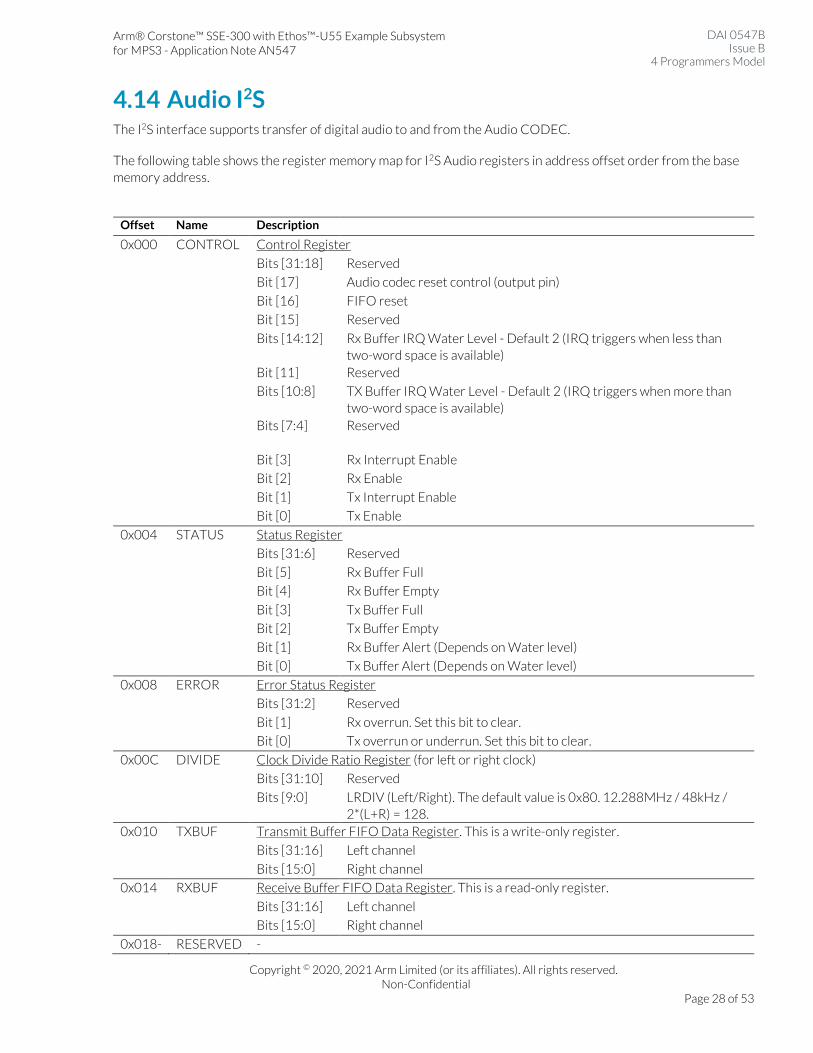
4.14 Audio I2S The I2S interface supports transfer of digital audio to and from the Audio CODEC.
The following table shows the register memory map for I2S Audio registers in address offset order from the base
memory address.
Offset Name Description
0x000 CONTROL Control Register
Bits [31:18] Reserved
Bit [17] Audio codec reset control (output pin)
Bit [16] FIFO reset
Bit [15] Reserved
Bits [14:12] Rx Buffer IRQ Water Level - Default 2 (IRQ triggers when less than
two-word space is available)
Bit [11] Reserved
Bits [10:8] TX Buffer IRQ Water Level - Default 2 (IRQ triggers when more than
two-word space is available)
Bits [7:4]
Reserved
Bit [3] Rx Interrupt Enable
Bit [2] Rx Enable
Bit [1] Tx Interrupt Enable
Bit [0] Tx Enable
0x004 STATUS Status Register
Bits [31:6] Reserved
Bit [5] Rx Buffer Full
Bit [4] Rx Buffer Empty
Bit [3] Tx Buffer Full
Bit [2] Tx Buffer Empty
Bit [1] Rx Buffer Alert (Depends on Water level)
Bit [0] Tx Buffer Alert (Depends on Water level)
0x008 ERROR Error Status Register
Bits [31:2] Reserved
Bit [1] Rx overrun. Set this bit to clear.
Bit [0] Tx overrun or underrun. Set this bit to clear.
0x00C DIVIDE Clock Divide Ratio Register (for left or right clock)
Bits [31:10] Reserved
Bits [9:0]
LRDIV (Left/Right). The default value is 0x80. 12.288MHz / 48kHz /
2*(L+R) = 128.
0x010 TXBUF Transmit Buffer FIFO Data Register. This is a write-only register.
Bits [31:16] Left channel
Bits [15:0] Right channel
0x014 RXBUF Receive Buffer FIFO Data Register. This is a read-only register.
Bits [31:16] Left channel
Bits [15:0] Right channel
0x018- RESERVED -
Arm® Corstone™ SSE-300 with Ethos™-U55 Example Subsystem for MPS3 - Application Note AN547
DAI 0547B Issue B
4 Programmers Model
Copyright © 2020, 2021 Arm Limited (or its affiliates). All rights reserved. Non-Confidential
Page 29 of 53
Offset Name Description
0x2FF
0x300 ITCR Integration Test Control Register
Bits [31:1] Reserved
Bit [0] ITCR
0x304 ITIP1 Integration Test Input Register 1
Bits [31:1] Reserved
Bit [0] SDIN
0x308 ITOP1 Integration Test Output Register 1
Bits [31:4] Reserved
Bit [3] IRQOUT
Bit [2] LRCK
Bit [1] SCLK
Bit [0] SDOUT
Table 4-4 Audio I2S Register Map
4.15 Audio Configuration The SMM implements a simple SBCon interface based on I2C. It configures the Cirrus Logic Low Power
Codec with Class D Speaker Driver, CS42L52 part on the MPS3 board.
Arm® Corstone™ SSE-300 with Ethos™-U55 Example Subsystem for MPS3 - Application Note AN547
DAI 0547B Issue B
4 Programmers Model
Copyright © 2020, 2021 Arm Limited (or its affiliates). All rights reserved. Non-Confidential
Page 30 of 53
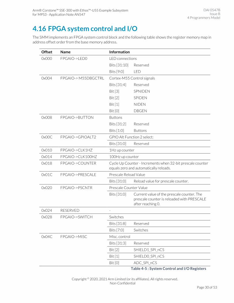
4.16 FPGA system control and I/O The SMM implements an FPGA system control block and the following table shows the register memory map in
address offset order from the base memory address.
Offset Name Information
0x000 FPGAIO->LED0 LED connections
Bits [31:10] Reserved
Bits [9:0] LED
0x004 FPGAIO-> M55DBGCTRL Cortex-M55 Control signals
Bits [31:4] Reserved
Bit [3] SPNIDEN
Bit [2] SPIDEN
Bit [1] NIDEN
Bit [0] DBGEN
0x008 FPGAIO->BUTTON Buttons
Bits [31:2] Reserved
Bits [1:0] Buttons
0x00C FPGAIO->GPIOALT2 GPIO Alt Function 2 select:
Bits [31:0] Reserved
0x010 FPGAIO->CLK1HZ 1Hz up counter
0x014 FPGAIO->CLK100HZ 100Hz up counter
0x018 FPGAIO->COUNTER Cycle Up Counter - Increments when 32-bit prescale counter
equals zero and automatically reloads.
0x01C FPGAIO->PRESCALE Prescale Reload Value
Bits [31:0] Reload value for prescale counter.
0x020 FPGAIO->PSCNTR Prescale Counter Value
Bits [31:0] Current value of the prescale counter. The
prescale counter is reloaded with PRESCALE
after reaching 0.
0x024 RESERVED -
0x028 FPGAIO->SWITCH Switches
Bits [31:8] Reserved
Bits [7:0] Switches
0x04C FPGAIO->MISC Misc. control
Bits [31:3] Reserved
Bit [2] SHIELD1_SPI_nCS
Bit [1] SHIELD0_SPI_nCS
Bit [0] ADC_SPI_nCS
Table 4-5 : System Control and I/O Registers
Arm® Corstone™ SSE-300 with Ethos™-U55 Example Subsystem for MPS3 - Application Note AN547
DAI 0547B Issue B
4 Programmers Model
Copyright © 2020, 2021 Arm Limited (or its affiliates). All rights reserved. Non-Confidential
Page 31 of 53
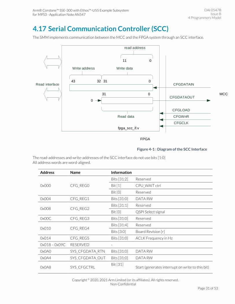
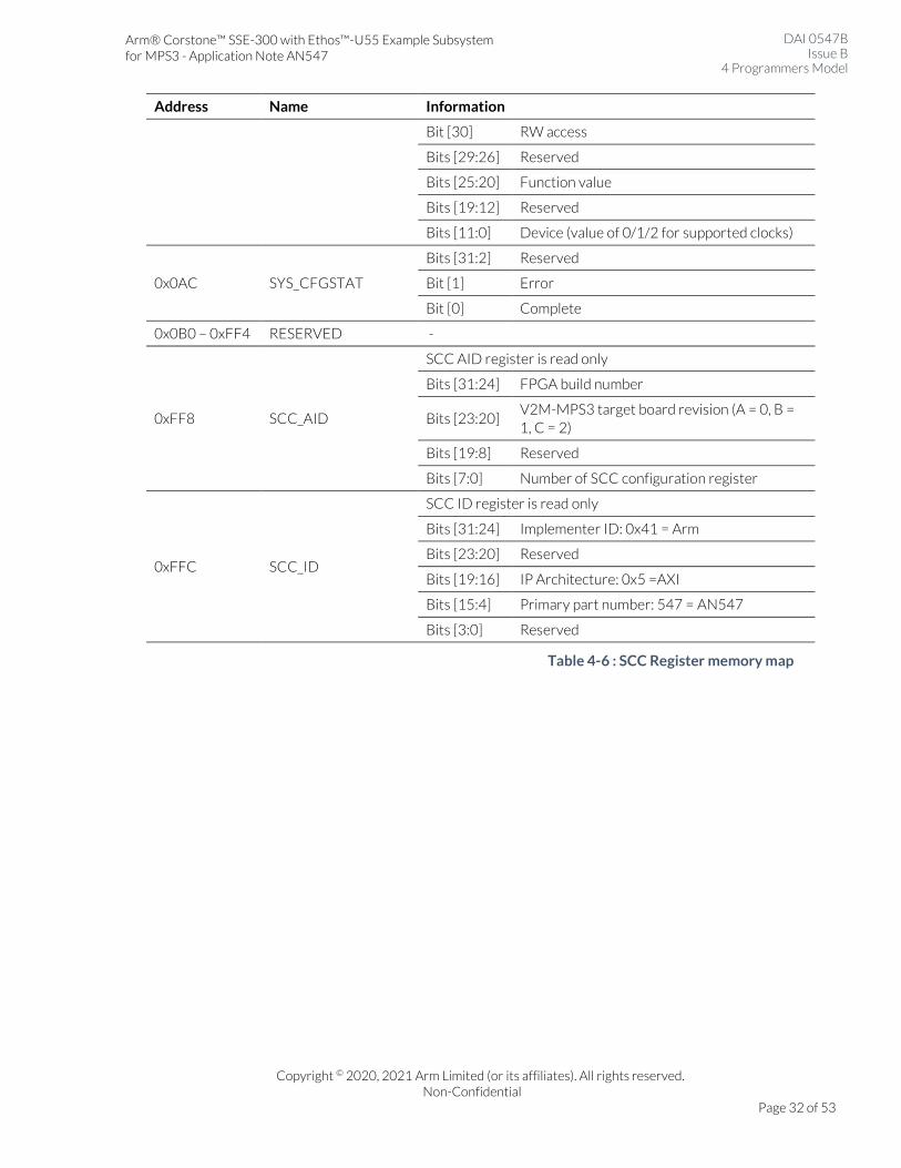
4.17 Serial Communication Controller (SCC) The SMM implements communication between the MCC and the FPGA system through an SCC interface.
FPGA
MCC
CFGDATAIN
CFGLOAD
CFGDATAOUT
CFGWnR
CFGCLK
0
31 0
43
Write address
3132
Write data
11
read address
0
0
Read data
fpga_scc_if.v
Read interface
Figure 4-1 : Diagram of the SCC Interface
The read-addresses and write-addresses of the SCC interface do not use bits [1:0]
All address words are word-aligned.
Address Name Information
0x000 CFG_REG0
Bits [31:2] Reserved
Bit [1] CPU_WAIT ctrl
Bit [0] Reserved
0x004 CFG_REG1 Bits [31:0] DATA RW
0x008 CFG_REG2 Bits [31:1] Reserved
Bit [0] QSPI Select signal
0x00C CFG_REG3 Bits [31:0] Reserved
0x010 CFG_REG4 Bits [31:4] Reserved
Bits [3:0] Board Revision [r]
0x014 CFG_REG5 Bits [31:0] ACLK Frequency in Hz
0x018 – 0x09C RESERVED -
0x0A0 SYS_CFGDATA_RTN Bits [31:0] DATA RW
0x0A4 SYS_CFGDATA_OUT Bits [31:0] DATA RW
0x0A8 SYS_CFGCTRL Bit [31]
Start (generates interrupt on write to this bit)
Arm® Corstone™ SSE-300 with Ethos™-U55 Example Subsystem for MPS3 - Application Note AN547
DAI 0547B Issue B
4 Programmers Model
Copyright © 2020, 2021 Arm Limited (or its affiliates). All rights reserved. Non-Confidential
Page 32 of 53
Address Name Information
Bit [30] RW access
Bits [29:26] Reserved
Bits [25:20] Function value
Bits [19:12] Reserved
Bits [11:0] Device (value of 0/1/2 for supported clocks)
0x0AC SYS_CFGSTAT
Bits [31:2] Reserved
Bit [1] Error
Bit [0] Complete
0x0B0 – 0xFF4 RESERVED -
0xFF8 SCC_AID
SCC AID register is read only
Bits [31:24] FPGA build number
Bits [23:20] V2M-MPS3 target board revision (A = 0, B =
1, C = 2)
Bits [19:8] Reserved
Bits [7:0] Number of SCC configuration register
0xFFC SCC_ID
SCC ID register is read only
Bits [31:24] Implementer ID: 0x41 = Arm
Bits [23:20] Reserved
Bits [19:16] IP Architecture: 0x5 =AXI
Bits [15:4] Primary part number: 547 = AN547
Bits [3:0] Reserved
Table 4-6 : SCC Register memory map
Arm® Corstone™ SSE-300 with Ethos™-U55 Example Subsystem for MPS3 - Application Note AN547
DAI 0547B Issue B
5 Clock architecture
Copyright © 2020, 2021 Arm Limited (or its affiliates). All rights reserved. Non-Confidential
Page 33 of 53
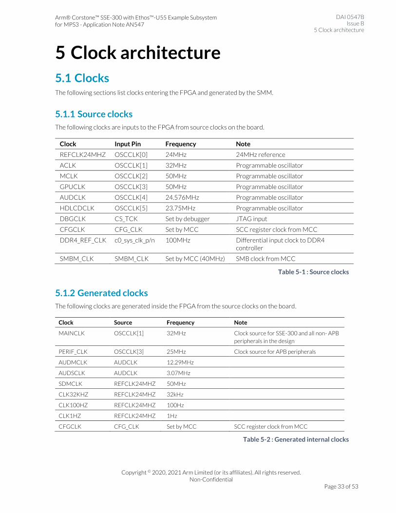
5 Clock architecture
5.1 Clocks The following sections list clocks entering the FPGA and generated by the SMM.
5.1.1 Source clocks
The following clocks are inputs to the FPGA from source clocks on the board.
Clock Input Pin Frequency Note
REFCLK24MHZ OSCCLK[0] 24MHz 24MHz reference
ACLK OSCCLK[1] 32MHz Programmable oscillator
MCLK OSCCLK[2] 50MHz Programmable oscillator
GPUCLK OSCCLK[3] 50MHz Programmable oscillator
AUDCLK OSCCLK[4] 24.576MHz Programmable oscillator
HDLCDCLK OSCCLK[5] 23.75MHz Programmable oscillator
DBGCLK CS_TCK Set by debugger JTAG input
CFGCLK CFG_CLK Set by MCC SCC register clock from MCC
DDR4_REF_CLK c0_sys_clk_p/n 100MHz Differential input clock to DDR4 controller
SMBM_CLK SMBM_CLK Set by MCC (40MHz) SMB clock from MCC
Table 5-1 : Source clocks
5.1.2 Generated clocks
The following clocks are generated inside the FPGA from the source clocks on the board.
Clock Source Frequency Note
MAINCLK OSCCLK[1] 32MHz Clock source for SSE-300 and all non- APB
peripherals in the design
PERIF_CLK OSCCLK[3] 25MHz Clock source for APB peripherals
AUDMCLK AUDCLK 12.29MHz
AUDSCLK AUDCLK 3.07MHz
SDMCLK REFCLK24MHZ 50MHz
CLK32KHZ REFCLK24MHZ 32kHz
CLK100HZ REFCLK24MHZ 100Hz
CLK1HZ REFCLK24MHZ 1Hz
CFGCLK CFG_CLK Set by MCC SCC register clock from MCC
Table 5-2 : Generated internal clocks
Arm® Corstone™ SSE-300 with Ethos™-U55 Example Subsystem for MPS3 - Application Note AN547
DAI 0547B Issue B
6 FPGA Secure Privilege Control
Copyright © 2020, 2021 Arm Limited (or its affiliates). All rights reserved. Non-Confidential
Page 34 of 53
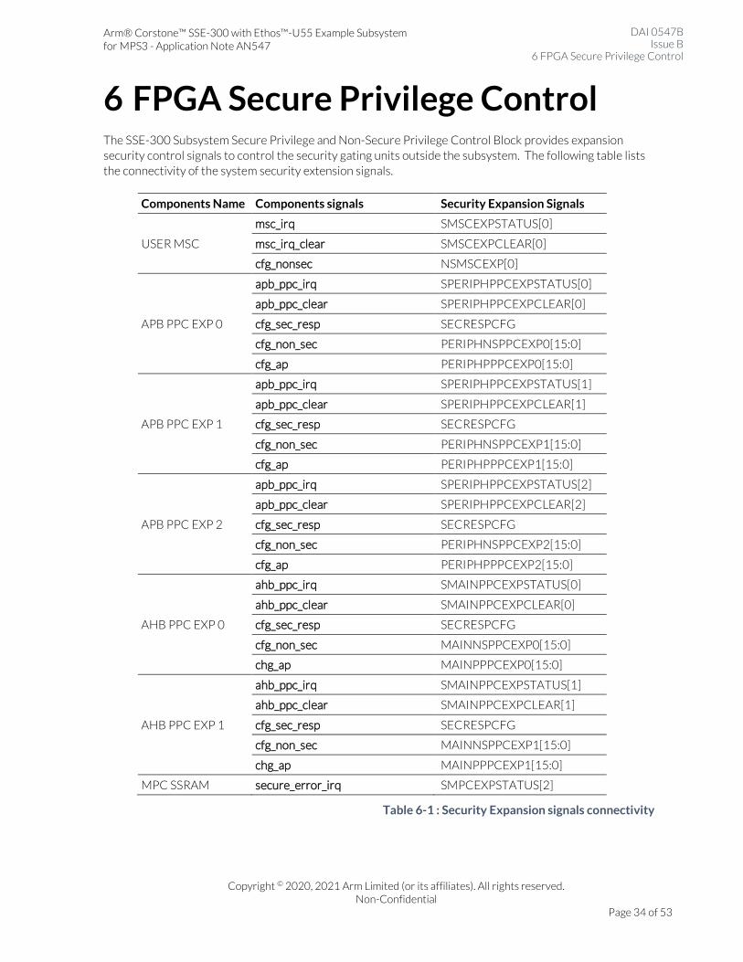
6 FPGA Secure Privilege Control The SSE-300 Subsystem Secure Privilege and Non-Secure Privilege Control Block provides expansion
security control signals to control the security gating units outside the subsystem. The following table lists
the connectivity of the system security extension signals.
Components Name Components signals Security Expansion Signals
USER MSC
msc_irq SMSCEXPSTATUS[0]
msc_irq_clear SMSCEXPCLEAR[0]
cfg_nonsec NSMSCEXP[0]
apb_ppc_irq SPERIPHPPCEXPSTATUS[0]
apb_ppc_clear SPERIPHPPCEXPCLEAR[0]
APB PPC EXP 0 cfg_sec_resp SECRESPCFG
cfg_non_sec PERIPHNSPPCEXP0[15:0]
cfg_ap PERIPHPPPCEXP0[15:0]
APB PPC EXP 1
apb_ppc_irq SPERIPHPPCEXPSTATUS[1]
apb_ppc_clear SPERIPHPPCEXPCLEAR[1]
cfg_sec_resp SECRESPCFG
cfg_non_sec PERIPHNSPPCEXP1[15:0]
cfg_ap PERIPHPPPCEXP1[15:0]
APB PPC EXP 2
apb_ppc_irq SPERIPHPPCEXPSTATUS[2]
apb_ppc_clear SPERIPHPPCEXPCLEAR[2]
cfg_sec_resp SECRESPCFG
cfg_non_sec PERIPHNSPPCEXP2[15:0]
cfg_ap PERIPHPPPCEXP2[15:0]
AHB PPC EXP 0
ahb_ppc_irq SMAINPPCEXPSTATUS[0]
ahb_ppc_clear SMAINPPCEXPCLEAR[0]
cfg_sec_resp SECRESPCFG
cfg_non_sec MAINNSPPCEXP0[15:0]
chg_ap MAINPPPCEXP0[15:0]
AHB PPC EXP 1
ahb_ppc_irq SMAINPPCEXPSTATUS[1]
ahb_ppc_clear SMAINPPCEXPCLEAR[1]
cfg_sec_resp SECRESPCFG
cfg_non_sec MAINNSPPCEXP1[15:0]
chg_ap MAINPPPCEXP1[15:0]
MPC SSRAM secure_error_irq SMPCEXPSTATUS[2]
Table 6-1 : Security Expansion signals connectivity
Arm® Corstone™ SSE-300 with Ethos™-U55 Example Subsystem for MPS3 - Application Note AN547
DAI 0547B Issue B
6 FPGA Secure Privilege Control
Copyright © 2020, 2021 Arm Limited (or its affiliates). All rights reserved. Non-Confidential
Page 35 of 53
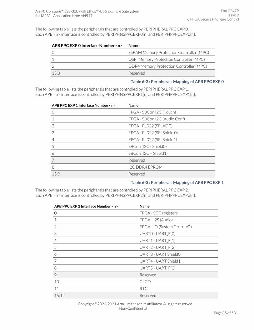
The following table lists the peripherals that are controlled by PERIPHERAL PPC EXP 0.
Each APB <n> interface is controlled by PERIPHNSPPCEXP0[n] and PERIPHPPPCEXP0[n].
APB PPC EXP 0 Interface Number <n> Name
0 SSRAM Memory Protection Controller (MPC)
1 QSPI Memory Protection Controller (MPC)
2 DDR4 Memory Protection Controller (MPC)
15:3 Reserved
Table 6-2 : Peripherals Mapping of APB PPC EXP 0
The following table lists the peripherals that are controlled by PERIPHERAL PPC EXP 1.
Each APB <n> interface is controlled by PERIPHNSPPCEXP1[n] and PERIPHPPPCEXP1[n].
APB PPC EXP 1 Interface Number <n> Name
0 FPGA - SBCon I2C (Touch)
1 FPGA - SBCon I2C (Audio Conf)
2 FPGA - PL022 (SPI ADC)
3 FPGA - PL022 (SPI Shield 0)
4 FPGA - PL022 (SPI Shield1)
5 SBCon (I2C - Shield0)
6 SBCon (I2C – Shield1)
7 Reserved
8 I2C DDR4 EPROM
15:9 Reserved
Table 6-3 : Peripherals Mapping of APB PPC EXP 1
The following table lists the peripherals that are controlled by PERIPHERAL PPC EXP 2.
Each APB <n> interface is controlled by PERIPHNSPPCEXP2[n] and PERIPHPPPCEXP2[n].
APB PPC EXP 2 Interface Number <n> Name
0 FPGA - SCC registers
1 FPGA - I2S (Audio)
2 FPGA - IO (System Ctrl + I/O)
3 UART0 - UART_F[0]
4 UART1 - UART_F[1]
5 UART2 - UART_F[2]
6 UART3 - UART Shield0
7 UART4 - UART Shield1
8 UART5 - UART_F[3]
9 Reserved
10 CLCD
11 RTC
15:12 Reserved
Arm® Corstone™ SSE-300 with Ethos™-U55 Example Subsystem for MPS3 - Application Note AN547
DAI 0547B Issue B
6 FPGA Secure Privilege Control
Copyright © 2020, 2021 Arm Limited (or its affiliates). All rights reserved. Non-Confidential
Page 36 of 53
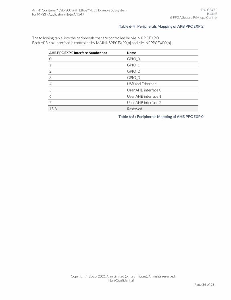
Table 6-4 : Peripherals Mapping of APB PPC EXP 2
The following table lists the peripherals that are controlled by MAIN PPC EXP 0.
Each APB <n> interface is controlled by MAINNSPPCEXP0[n] and MAINPPPCEXP0[n].
AHB PPC EXP 0 Interface Number <n> Name
0 GPIO_0
1 GPIO_1
2 GPIO_2
3 GPIO_3
4 USB and Ethernet
5 User AHB interface 0
6 User AHB interface 1
7 User AHB interface 2
15:8 Reserved
Table 6-5 : Peripherals Mapping of AHB PPC EXP 0
Arm® Corstone™ SSE-300 with Ethos™-U55 Example Subsystem for MPS3 - Application Note AN547
DAI 0547B Issue B
7 Interrupt Map
Copyright © 2020, 2021 Arm Limited (or its affiliates). All rights reserved. Non-Confidential
Page 37 of 53
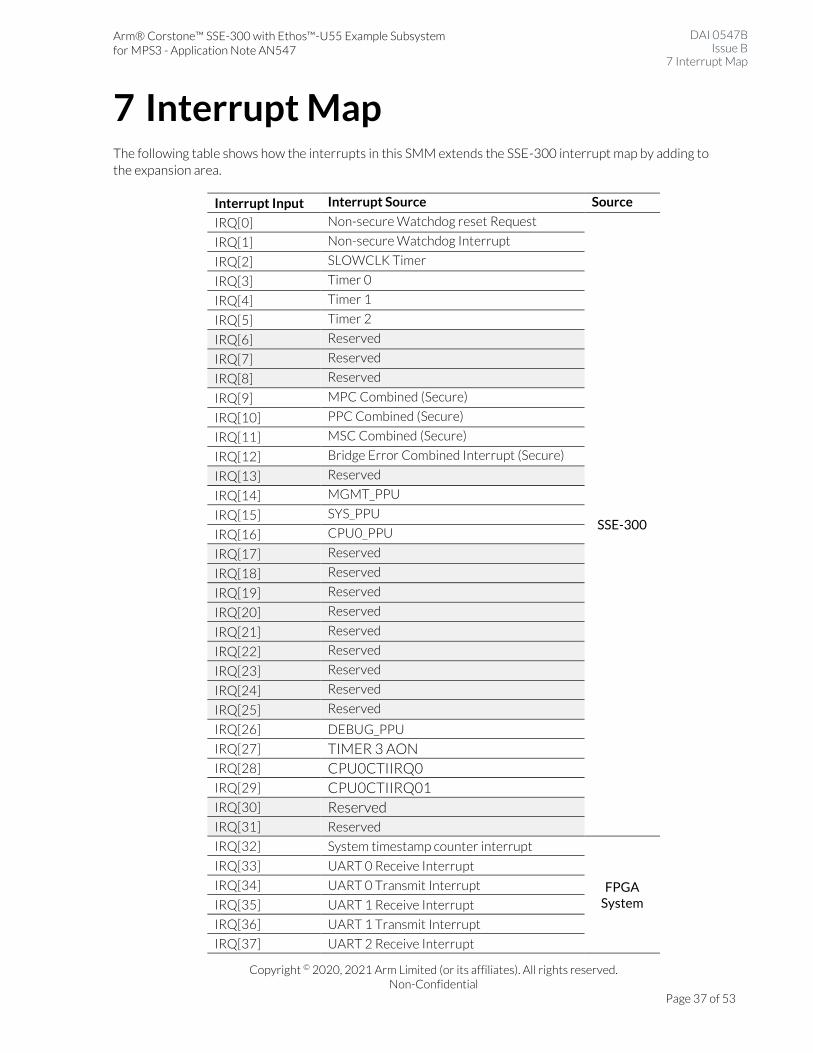
7 Interrupt Map The following table shows how the interrupts in this SMM extends the SSE-300 interrupt map by adding to
the expansion area.
Interrupt Input Interrupt Source Source
IRQ[0] Non-secure Watchdog reset Request
SSE-300
IRQ[1] Non-secure Watchdog Interrupt
IRQ[2] SLOWCLK Timer
IRQ[3] Timer 0
IRQ[4] Timer 1
IRQ[5] Timer 2
IRQ[6] Reserved
IRQ[7] Reserved
IRQ[8] Reserved
IRQ[9] MPC Combined (Secure)
IRQ[10] PPC Combined (Secure)
IRQ[11] MSC Combined (Secure)
IRQ[12] Bridge Error Combined Interrupt (Secure)
IRQ[13] Reserved
IRQ[14] MGMT_PPU
IRQ[15] SYS_PPU
IRQ[16] CPU0_PPU
IRQ[17] Reserved
IRQ[18] Reserved
IRQ[19] Reserved
IRQ[20] Reserved
IRQ[21] Reserved
IRQ[22] Reserved
IRQ[23] Reserved
IRQ[24] Reserved
IRQ[25] Reserved
IRQ[26] DEBUG_PPU
IRQ[27] TIMER 3 AON
IRQ[28] CPU0CTIIRQ0
IRQ[29] CPU0CTIIRQ01
IRQ[30] Reserved
IRQ[31] Reserved
IRQ[32] System timestamp counter interrupt
FPGA System
IRQ[33] UART 0 Receive Interrupt
IRQ[34] UART 0 Transmit Interrupt
IRQ[35] UART 1 Receive Interrupt
IRQ[36] UART 1 Transmit Interrupt
IRQ[37] UART 2 Receive Interrupt
Arm® Corstone™ SSE-300 with Ethos™-U55 Example Subsystem for MPS3 - Application Note AN547
DAI 0547B Issue B
7 Interrupt Map
Copyright © 2020, 2021 Arm Limited (or its affiliates). All rights reserved. Non-Confidential
Page 38 of 53
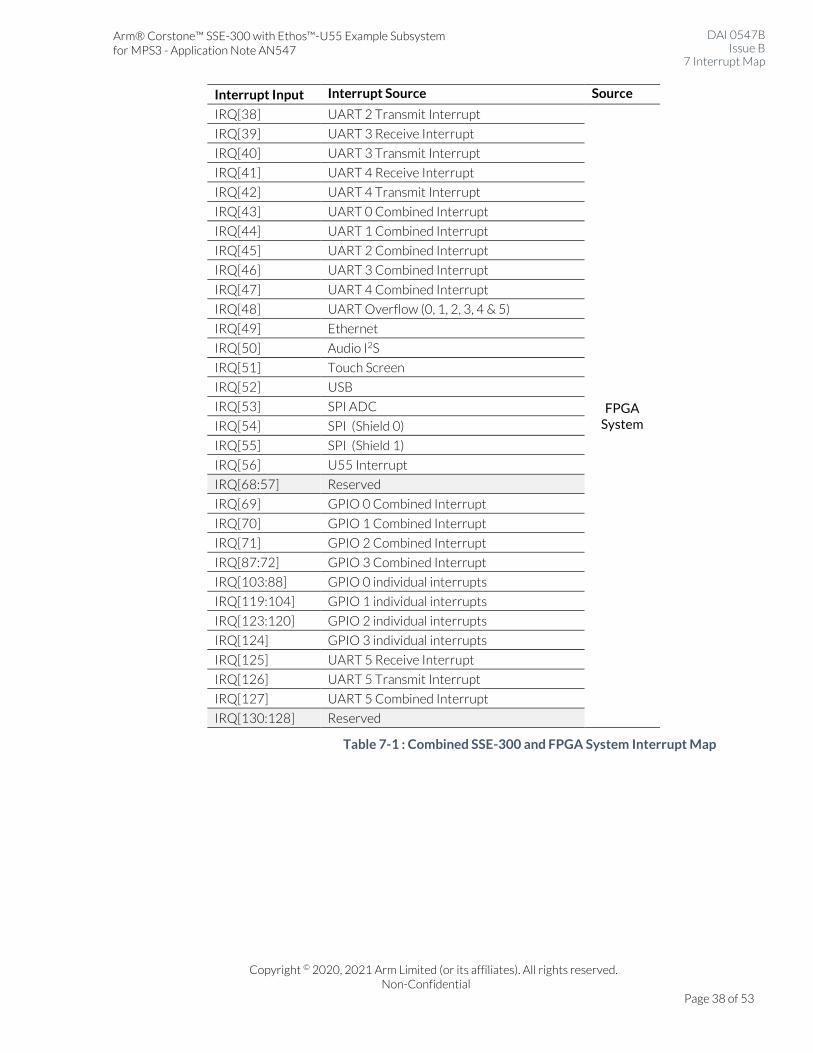
Interrupt Input Interrupt Source Source
IRQ[38] UART 2 Transmit Interrupt
FPGA System
IRQ[39] UART 3 Receive Interrupt
IRQ[40] UART 3 Transmit Interrupt
IRQ[41] UART 4 Receive Interrupt
IRQ[42] UART 4 Transmit Interrupt
IRQ[43] UART 0 Combined Interrupt
IRQ[44] UART 1 Combined Interrupt
IRQ[45] UART 2 Combined Interrupt
IRQ[46] UART 3 Combined Interrupt
IRQ[47] UART 4 Combined Interrupt
IRQ[48] UART Overflow (0, 1, 2, 3, 4 & 5)
IRQ[49] Ethernet
IRQ[50] Audio I2S
IRQ[51] Touch Screen
IRQ[52] USB
IRQ[53] SPI ADC
IRQ[54] SPI (Shield 0)
IRQ[55] SPI (Shield 1)
IRQ[56] U55 Interrupt
IRQ[68:57] Reserved
IRQ[69] GPIO 0 Combined Interrupt
IRQ[70] GPIO 1 Combined Interrupt
IRQ[71] GPIO 2 Combined Interrupt
IRQ[87:72] GPIO 3 Combined Interrupt
IRQ[103:88] GPIO 0 individual interrupts
IRQ[119:104] GPIO 1 individual interrupts
IRQ[123:120] GPIO 2 individual interrupts
IRQ[124] GPIO 3 individual interrupts
IRQ[125] UART 5 Receive Interrupt
IRQ[126] UART 5 Transmit Interrupt
IRQ[127] UART 5 Combined Interrupt
IRQ[130:128] Reserved
Table 7-1 : Combined SSE-300 and FPGA System Interrupt Map
Arm® Corstone™ SSE-300 with Ethos™-U55 Example Subsystem for MPS3 - Application Note AN547
DAI 0547B Issue B
7 Interrupt Map
Copyright © 2020, 2021 Arm Limited (or its affiliates). All rights reserved. Non-Confidential
Page 39 of 53
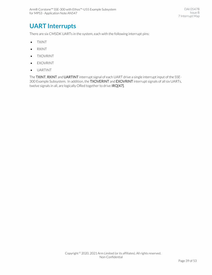
UART Interrupts There are six CMSDK UARTs in the system, each with the following interrupt pins:
• TXINT
• RXINT
• TXOVRINT
• EXOVRINT
• UARTINT
The TXINT, RXINT and UARTINT interrupt signal of each UART drive a single interrupt input of the SSE-
300 Example Subsystem. In addition, the TXOVERINT and EXOVRINT interrupt signals of all six UARTs,
twelve signals in all, are logically ORed together to drive IRQ[47].
Arm® Corstone™ SSE-300 with Ethos™-U55 Example Subsystem for MPS3 Application Note AN547
DAI 0547B Issue B
8 Shield Support
Copyright © 2020, 2021 Arm Limited (or its affiliates). All rights reserved. Non-Confidential
Page 40 of 53
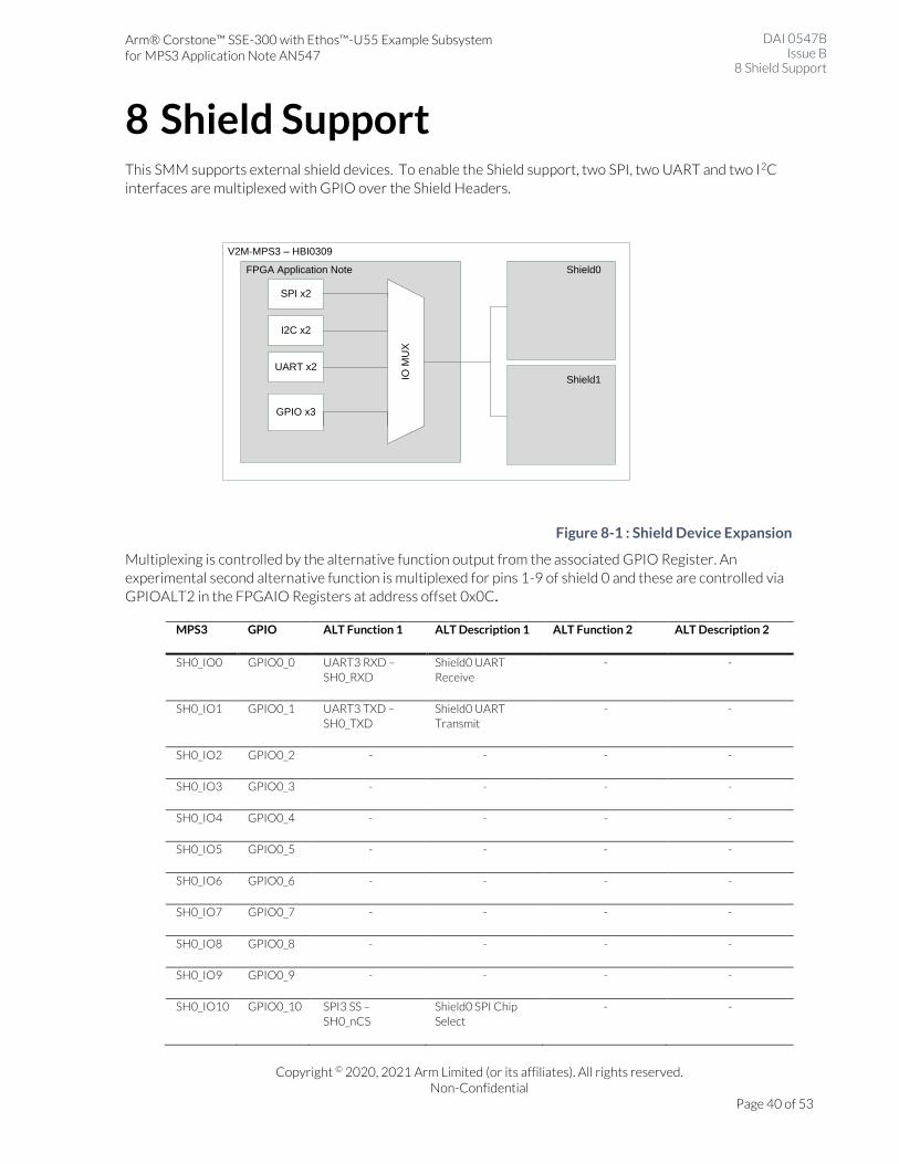
8 Shield Support This SMM supports external shield devices. To enable the Shield support, two SPI, two UART and two I2C
interfaces are multiplexed with GPIO over the Shield Headers.
GPIO x3
UART x2
SPI x2
I2C x2
IO M
UX
V2M-MPS3 – HBI0309
FPGA Application Note Shield0
Shield1
Figure 8-1 : Shield Device Expansion
Multiplexing is controlled by the alternative function output from the associated GPIO Register. An
experimental second alternative function is multiplexed for pins 1-9 of shield 0 and these are controlled via
GPIOALT2 in the FPGAIO Registers at address offset 0x0C.
MPS3 GPIO ALT Function 1 ALT Description 1 ALT Function 2 ALT Description 2
SH0_IO0 GPIO0_0 UART3 RXD –
SH0_RXD
Shield0 UART
Receive
- -
SH0_IO1 GPIO0_1 UART3 TXD –
SH0_TXD
Shield0 UART
Transmit
- -
SH0_IO2 GPIO0_2 - - - -
SH0_IO3 GPIO0_3 - - - -
SH0_IO4 GPIO0_4 - - - -
SH0_IO5 GPIO0_5 - - - -
SH0_IO6 GPIO0_6 - - - -
SH0_IO7 GPIO0_7 - - - -
SH0_IO8 GPIO0_8 - - - -
SH0_IO9 GPIO0_9 - - - -
SH0_IO10 GPIO0_10 SPI3 SS –
SH0_nCS
Shield0 SPI Chip
Select
- -
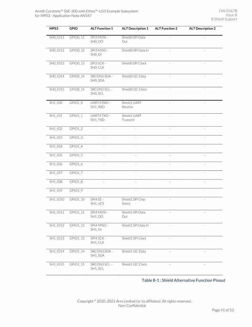
Arm® Corstone™ SSE-300 with Ethos™-U55 Example Subsystem for MPS3 - Application Note AN547
DAI 0547B Issue B
8 Shield Support
Copyright © 2020, 2021 Arm Limited (or its affiliates). All rights reserved. Non-Confidential
Page 41 of 53
MPS3 GPIO ALT Function 1 ALT Description 1 ALT Function 2 ALT Description 2
SH0_IO11 GPIO0_11 SPI3 MOSI –
SH0_DO
Shield0 SPI Data
Out
- -
SH0_IO12 GPIO0_12 SPI3 MISO –
SH0_DI
Shield0 SPI Data In - -
SH0_IO13 GPIO0_13 SPI3 SCK –
SH0_CLK
Shield0 SPI Clock - -
SH0_IO14 GPIO0_14 SBCON2 SDA –
SH0_SDA
Shield0 I2C Data - -
SH0_IO15 GPIO0_15 SBCON2 SCL –
SH0_SCL
Shield0 I2C Clock - -
SH1_IO0 GPIO1_0 UART4 RXD –
SH1_RXD
Shield1 UART
Receive
- -
SH1_IO1 GPIO1_1 UART4 TXD –
SH1_TXD
Shield1 UART
Transmit
- -
SH1_IO2 GPIO1_2 - - - -
SH1_IO3 GPIO1_3 - - - -
SH1_IO4 GPIO1_4 - - - -
SH1_IO5 GPIO1_5 - - - -
SH1_IO6 GPIO1_6 - - - -
SH1_IO7 GPIO1_7 - - - -
SH1_IO8 GPIO1_8 - - - -
SH1_IO9 GPIO1_9 - - - -
SH1_IO10 GPIO1_10 SPI4 SS –
SH1_nCS
Shield1 SPI Chip
Select
- -
SH1_IO11 GPIO1_11 SPI4 MOSI –
SH1_DO
Shield1 SPI Data
Out
- -
SH1_IO12 GPIO1_12 SPI4 MISO –
SH1_DI
Shield1 SPI Data In - -
SH1_IO13 GPIO1_13 SPI4 SCK –
SH1_CLK
Shield1 SPI Clock - -
SH1_IO14 GPIO1_14 SBCON3 SDA –
SH1_SDA
Shield1 I2C Data - -
SH1_IO15 GPIO1_15 SBCON3 SCL –
SH1_SCL
Shield1 I2C Clock - -
Table 8-1 : Shield Alternative Function Pinout
Arm® Corstone™ SSE-300 with Ethos™-U55 Example Subsystem for MPS3 - Application Note AN547
DAI 0547B Issue B
9 Using AN547 on the MPS3 Board
Copyright © 2020, 2021 Arm Limited (or its affiliates). All rights reserved. Non-Confidential
Page 42 of 53
9 Using AN547 on the MPS3 Board
9.1 Pre-Requisites Familiarity with MPS3:
• Familiarisation with the Arm® MPS3 FPGA Prototyping Board Technical Reference Manual.
• Understanding of the configuration and boot flow described in the MPS3 TRM.
Ensure you have gained familiarity with the MPS3 board and are able to:
1. Connect a PC to the MPS3 board using a USB connection (which is required to load files onto the MPS3 board SD card to run the built .bit file from the FPGA build flow).
2. Power the MPS3 board.
3. The MPS3 board appears as a mapped drive named “V2M_MPS3”.
4. Understand how to power up, reset and establish a serial terminal over the USB connection to a host PC.
9.2 Loading a prebuilt image onto the MPS3 Board To load the prebuilt AN547 image, follow these steps:
1. Power up the MPS3 board using the PBON push button and wait for the V2M_MPS3 drive to appear.
2. Format the V2M_MPS3 drive and copy the contents of <install_dir>/Boardfiles and paste them
into the root directory of the attached V2M_MPS3 drive.
Note: You might want to manually modify and merge the contents for certain configuration files. Alternatively, you can restore the existing configuration files from the /Boardfiles directory. The affected
configuration files are:
a. <install_dir>/Boardfiles/config.txt
b. <install_dir>/Boardfiles/MB/HBI0309C/board.txt
3. Eject the V2M_MPS3 volume from your computer to unmount the drive.
4. Power cycle the MPS3 board using the PBRST push button and then launch MCC firmware update and FPGA configuration by pressing PBON push button. The LEDs flash rapidly to indicate that a new MCC firmware is being downloaded, (this only occurs the first time the MCC firmware is updated), and that the prebuilt image is being downloaded onto the board. When the bar LEDs next to PBRST button show green and user LED’s UL0-7 are alternatively lit, the FPGA is programmed.
5. The color LCD touch screen shows the MPS3 splash screen. Simultaneously, if you have configured the UART to run, the debug UART terminal shows the selftest menu for Application Note AN547.
6. If the MPS3 board does not boot correctly, refer to the log.txt in the root directory of the MPS3 board
which provides a log file of the files loaded at bootup.
Arm® Corstone™ SSE-300 with Ethos™-U55 Example Subsystem for MPS3 - Application Note AN547
DAI 0547B Issue B
9 Using AN547 on the MPS3 Board
Copyright © 2020, 2021 Arm Limited (or its affiliates). All rights reserved. Non-Confidential
Page 43 of 53
9.3 UART Serial Ports Four serial ports are supported on this implementation and are accessible through the MPS3 board Debug USB
port:
• Serial Port 0 is connected to the MCC and outputs debug information about the status of the MCC.
• Serial Port 1 is connected to the UART 0.
• Serial Port 2 is connected to the UART 1.
• Serial Port 3 is connected to the UART 2.
Note
The logical<>physical mapping of the serial ports on a host PC can be confusing due to the way the driver may
allocate the port numbers. The serial port presented with the lowest number aligns to Serial Port 0 above.
9.4 UART Serial Port Terminal Emulator Settings All serial ports on this implementation use the following terminal/serial port settings:
Baud Rate: 115200 bps
New-Line: CR (Serial port 0) And LF (Serial Port 1,2 and 3 Only)
Data: 8 bits
Parity: none
Stop: 1 bit
Flow control: none
9.5 MPS3 USB Serial port drivers for Windows Information on installing drivers to support USB serial port on MPS3 can be found at:
https://community.arm.com/dev-platforms/w/docs/381/accessing-mps3-serial-ports-in-windows-10
Arm® Corstone™ SSE-300 with Ethos™-U55 Example Subsystem for MPS3 - Application Note AN547
DAI 0547B Issue B
10 Software
Copyright © 2020, 2021 Arm Limited (or its affiliates). All rights reserved. Non-Confidential
Page 44 of 53
10 Software
10.1 Rebuilding software Requirements:
• The software directory from the download
• Keil uVision 5.31 or later
The following instructions apply to the software package provided:
1. Navigate to <install_dir>/Software/selftest/Build_Keil/
2. Load selftest_mpb.uvprojx in Keil uVision
3. Once loaded, the project can be rebuilt by selecting either:
o Project - > Build Target
o Project - > Rebuild all target files
• The output can then be found in <install_dir>/Software/selftest/Build_Keil/an547_st.axf
10.2 Loading software on the MPS3 board Requirements:
• MPS3 board powered and USB cable connected
• MPS3 USB mass storage open in a file explorer
The following instructions apply to all versions of software:
1. Copy the software <install_dir>/Software/selftest/Build_Keil/an547_st.axf to the
board <MPS3_dir>/Software folder
2. Navigate to <MPS3_dir>MB/HBI0309C/AN547 and open the images.txt file in a text editor
3. Add a new line for the new software you wish to run and make sure the other lines are commented out, for example :
;IMAGE0FILE: \SOFTWARE\selftest.axf; - selftest uSD
IMAGE0FILE: \SOFTWARE\an547_st.axf ; - selftest uSD
(the compiled an547_st.axf image is uncommented, which is therefore selected and selftest.axf
is commented out)
The MPS3 can now be booted according to the instructions in the Arm® MPS3 FPGA Prototyping Board Getting
Started Guide accompanying the MPS3 board.
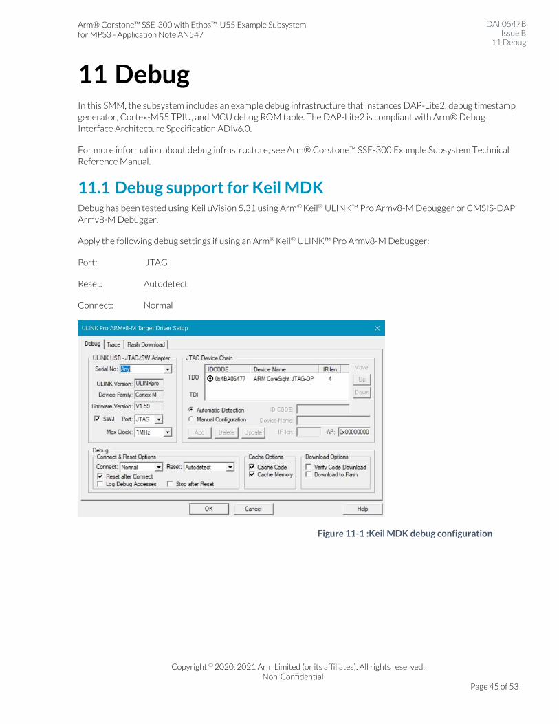
Arm® Corstone™ SSE-300 with Ethos™-U55 Example Subsystem for MPS3 - Application Note AN547
DAI 0547B Issue B
11 Debug
Copyright © 2020, 2021 Arm Limited (or its affiliates). All rights reserved. Non-Confidential
Page 45 of 53
11 Debug In this SMM, the subsystem includes an example debug infrastructure that instances DAP-Lite2, debug timestamp
generator, Cortex-M55 TPIU, and MCU debug ROM table. The DAP-Lite2 is compliant with Arm® Debug
Interface Architecture Specification ADIv6.0.
For more information about debug infrastructure, see Arm® Corstone™ SSE-300 Example Subsystem Technical
Reference Manual.
11.1 Debug support for Keil MDK Debug has been tested using Keil uVision 5.31 using Arm® Keil® ULINK™ Pro Armv8-M Debugger or CMSIS-DAP
Armv8-M Debugger.
Apply the following debug settings if using an Arm® Keil® ULINK™ Pro Armv8-M Debugger:
Port: JTAG
Reset: Autodetect
Connect: Normal
Figure 11-1 :Keil MDK debug configuration
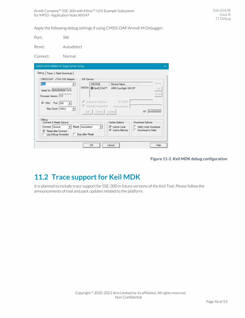
Arm® Corstone™ SSE-300 with Ethos™-U55 Example Subsystem for MPS3 - Application Note AN547
DAI 0547B Issue B
11 Debug
Copyright © 2020, 2021 Arm Limited (or its affiliates). All rights reserved. Non-Confidential
Page 46 of 53
Apply the following debug settings if using CMSIS-DAP Armv8-M Debugger:
Port: SW
Reset: Autodetect
Connect: Normal
Figure 11-2 :Keil MDK debug configuration
11.2 Trace support for Keil MDK It is planned to include trace support for SSE-300 in future versions of the Keil Tool. Please follow the
announcements of tool and pack updates related to the platform.
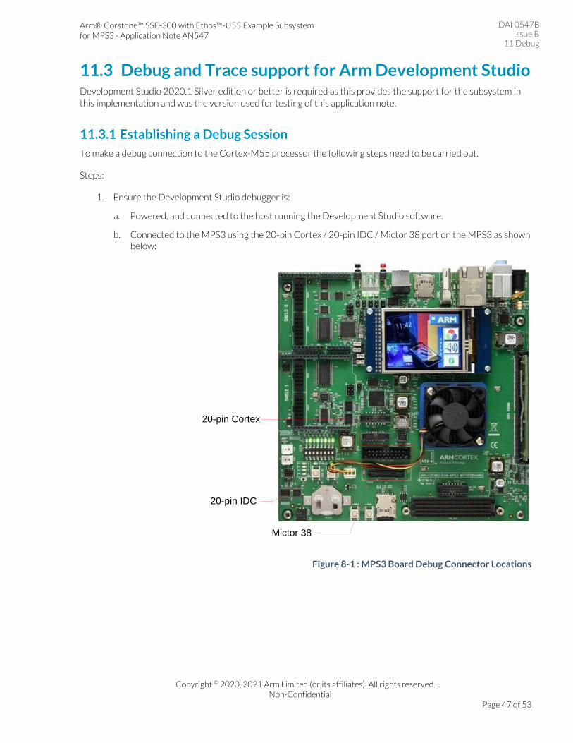
Arm® Corstone™ SSE-300 with Ethos™-U55 Example Subsystem for MPS3 - Application Note AN547
DAI 0547B Issue B
11 Debug
Copyright © 2020, 2021 Arm Limited (or its affiliates). All rights reserved. Non-Confidential
Page 47 of 53
11.3 Debug and Trace support for Arm Development Studio Development Studio 2020.1 Silver edition or better is required as this provides the support for the subsystem in
this implementation and was the version used for testing of this application note.
11.3.1 Establishing a Debug Session
To make a debug connection to the Cortex-M55 processor the following steps need to be carried out.
Steps:
1. Ensure the Development Studio debugger is:
a. Powered, and connected to the host running the Development Studio software.
b. Connected to the MPS3 using the 20-pin Cortex / 20-pin IDC / Mictor 38 port on the MPS3 as shown below:
20-pin Cortex
20-pin IDC
Mictor 38
Figure 8-1 : MPS3 Board Debug Connector Locations
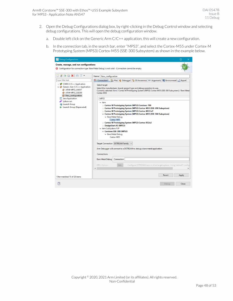
Arm® Corstone™ SSE-300 with Ethos™-U55 Example Subsystem for MPS3 - Application Note AN547
DAI 0547B Issue B
11 Debug
Copyright © 2020, 2021 Arm Limited (or its affiliates). All rights reserved. Non-Confidential
Page 48 of 53
2. Open the Debug Configurations dialog box, by right-clicking in the Debug Control window and selecting debug configurations. This will open the debug configuration window.
a. Double left click on the Generic Arm C/C++ application, this will create a new configuration.
b. In the connection tab, in the search bar, enter “MPS3”, and select the Cortex-M55 under Cortex-M Prototyping System (MPS3) Cortex-M55 (SSE-300 Subsystem) as shown in the example below.
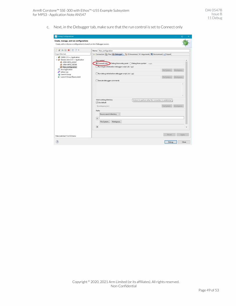
Arm® Corstone™ SSE-300 with Ethos™-U55 Example Subsystem for MPS3 - Application Note AN547
DAI 0547B Issue B
11 Debug
Copyright © 2020, 2021 Arm Limited (or its affiliates). All rights reserved. Non-Confidential
Page 49 of 53
c. Next, in the Debugger tab, make sure that the run control is set to Connect only
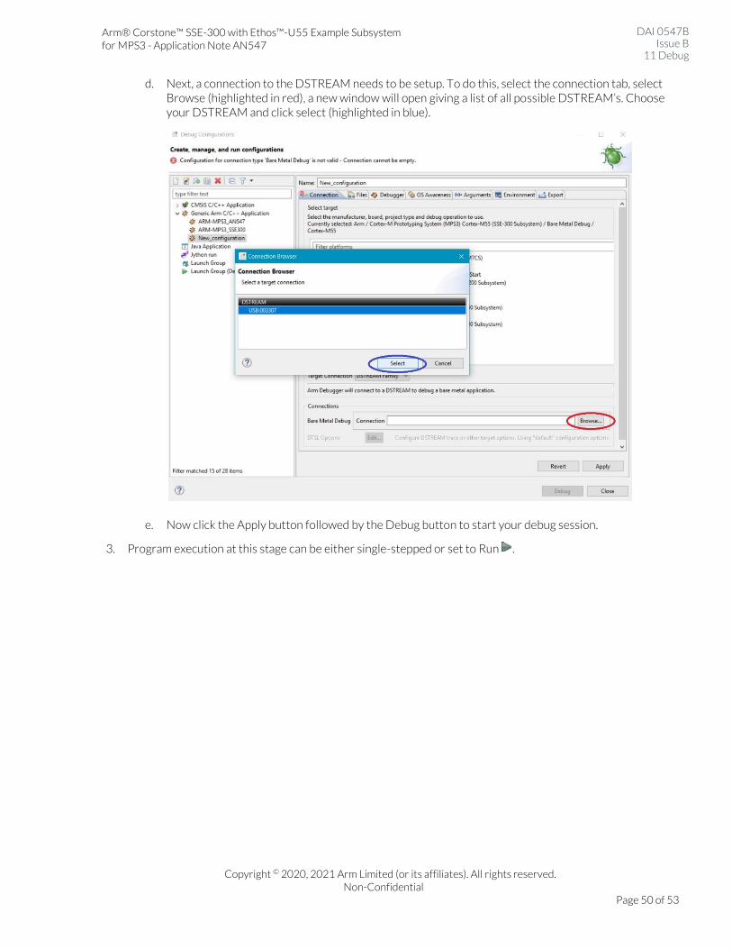
Arm® Corstone™ SSE-300 with Ethos™-U55 Example Subsystem for MPS3 - Application Note AN547
DAI 0547B Issue B
11 Debug
Copyright © 2020, 2021 Arm Limited (or its affiliates). All rights reserved. Non-Confidential
Page 50 of 53
d. Next, a connection to the DSTREAM needs to be setup. To do this, select the connection tab, select Browse (highlighted in red), a new window will open giving a list of all possible DSTREAM’s. Choose your DSTREAM and click select (highlighted in blue).
e. Now click the Apply button followed by the Debug button to start your debug session.
3. Program execution at this stage can be either single-stepped or set to Run .
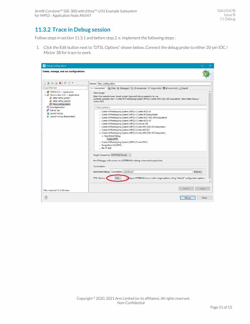
Arm® Corstone™ SSE-300 with Ethos™-U55 Example Subsystem for MPS3 - Application Note AN547
DAI 0547B Issue B
11 Debug
Copyright © 2020, 2021 Arm Limited (or its affiliates). All rights reserved. Non-Confidential
Page 51 of 53
11.3.2 Trace in Debug session
Follow steps in section 11.3.1 and before step 2. e. implement the following steps :
1. Click the Edit button next to “DTSL Options” shown below. Connect the debug probe to either 20-pin IDC /
Mictor 38 for trace to work.
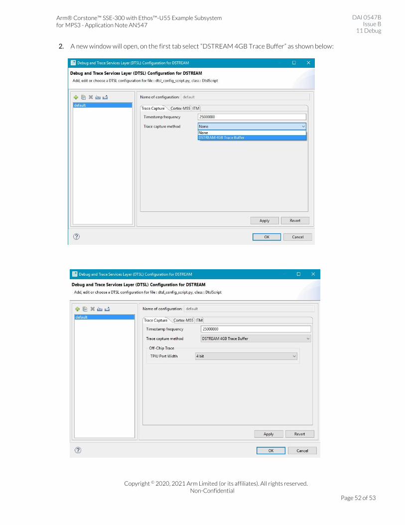
Arm® Corstone™ SSE-300 with Ethos™-U55 Example Subsystem for MPS3 - Application Note AN547
DAI 0547B Issue B
11 Debug
Copyright © 2020, 2021 Arm Limited (or its affiliates). All rights reserved. Non-Confidential
Page 52 of 53
2. A new window will open, on the first tab select “DSTREAM 4GB Trace Buffer” as shown below:
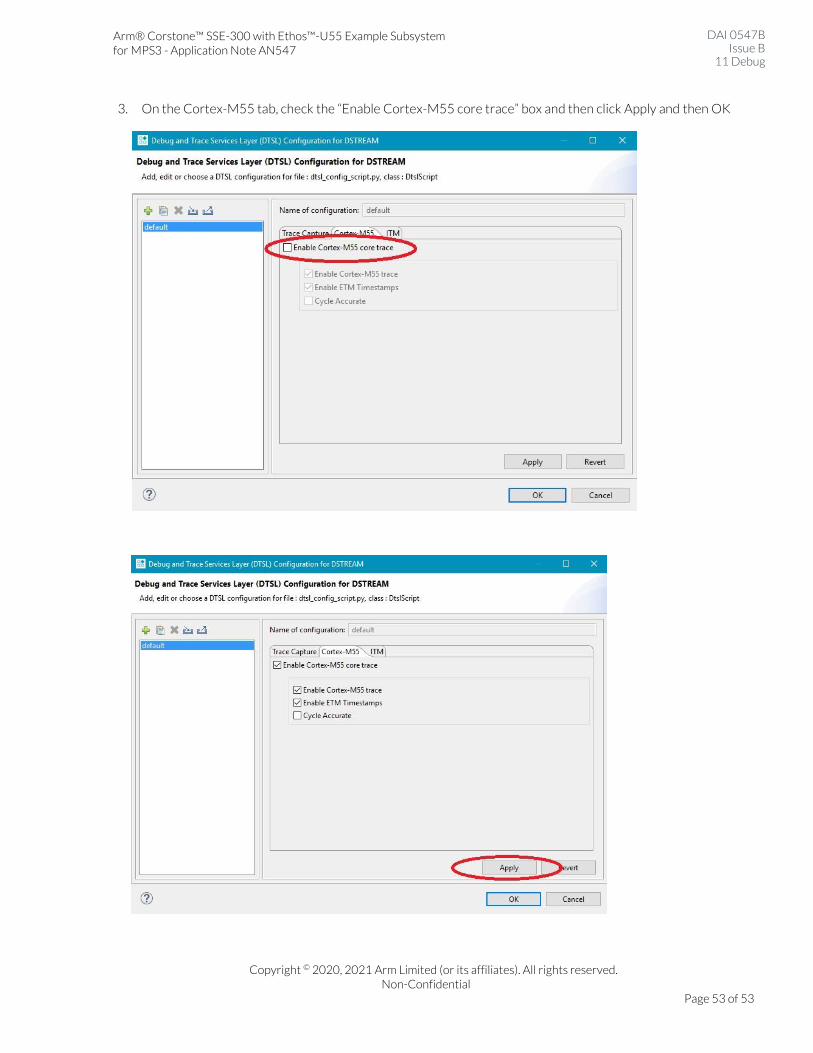
Arm® Corstone™ SSE-300 with Ethos™-U55 Example Subsystem for MPS3 - Application Note AN547
DAI 0547B Issue B
11 Debug
Copyright © 2020, 2021 Arm Limited (or its affiliates). All rights reserved. Non-Confidential
Page 53 of 53
3. On the Cortex-M55 tab, check the “Enable Cortex-M55 core trace” box and then click Apply and then OK