Embed Size (px)
Citation preview
This is information on a product in full production.
February 2021 DS11532 Rev 7 1/252
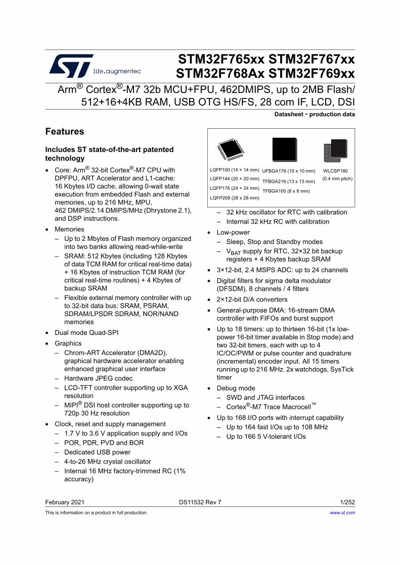
STM32F765xx STM32F767xx STM32F768Ax STM32F769xx
Arm® Cortex®-M7 32b MCU+FPU, 462DMIPS, up to 2MB Flash/ 512+16+4KB RAM, USB OTG HS/FS, 28 com IF, LCD, DSI
Datasheet - production data
Features
Includes ST state-of-the-art patented technology
• Core: Arm® 32-bit Cortex®-M7 CPU with DPFPU, ART Accelerator and L1-cache: 16 Kbytes I/D cache, allowing 0-wait state execution from embedded Flash and external memories, up to 216 MHz, MPU, 462 DMIPS/2.14 DMIPS/MHz (Dhrystone 2.1), and DSP instructions.
• Memories
– Up to 2 Mbytes of Flash memory organized into two banks allowing read-while-write
– SRAM: 512 Kbytes (including 128 Kbytes of data TCM RAM for critical real-time data) + 16 Kbytes of instruction TCM RAM (for critical real-time routines) + 4 Kbytes of backup SRAM
– Flexible external memory controller with up to 32-bit data bus: SRAM, PSRAM, SDRAM/LPSDR SDRAM, NOR/NAND memories
• Dual mode Quad-SPI
• Graphics
– Chrom-ART Accelerator (DMA2D), graphical hardware accelerator enabling enhanced graphical user interface
– Hardware JPEG codec
– LCD-TFT controller supporting up to XGA resolution
– MIPI® DSI host controller supporting up to 720p 30 Hz resolution
• Clock, reset and supply management
– 1.7 V to 3.6 V application supply and I/Os
– POR, PDR, PVD and BOR
– Dedicated USB power
– 4-to-26 MHz crystal oscillator
– Internal 16 MHz factory-trimmed RC (1% accuracy)
– 32 kHz oscillator for RTC with calibration
– Internal 32 kHz RC with calibration
• Low-power
– Sleep, Stop and Standby modes
– VBAT supply for RTC, 32×32 bit backup registers + 4 Kbytes backup SRAM
• 3×12-bit, 2.4 MSPS ADC: up to 24 channels
• Digital filters for sigma delta modulator (DFSDM), 8 channels / 4 filters
• 2×12-bit D/A converters
• General-purpose DMA: 16-stream DMA controller with FIFOs and burst support
• Up to 18 timers: up to thirteen 16-bit (1x low- power 16-bit timer available in Stop mode) and two 32-bit timers, each with up to 4 IC/OC/PWM or pulse counter and quadrature (incremental) encoder input. All 15 timers running up to 216 MHz. 2x watchdogs, SysTick timer
• Debug mode
– SWD and JTAG interfaces
– Cortex®-M7 Trace Macrocell™
• Up to 168 I/O ports with interrupt capability
– Up to 164 fast I/Os up to 108 MHz
– Up to 166 5 V-tolerant I/Os
LQFP100 (14 × 14 mm) UFBGA176 (10 x 10 mm)
TFBGA216 (13 x 13 mm)
LQFP208 (28 x 28 mm)
WLCSP180
(0.4 mm pitch)
LQFP176 (24 × 24 mm)
LQFP144 (20 × 20 mm)
TFBGA100 (8 x 8 mm)
www.st.com
STM32F765xx STM32F767xx STM32F768Ax STM32F769xx
2/252 DS11532 Rev 7
• Up to 28 communication interfaces
– Up to 4 I2C interfaces (SMBus/PMBus)
– Up to 4 USARTs/4 UARTs (12.5 Mbit/s, ISO7816 interface, LIN, IrDA, modem control)
– Up to 6 SPIs (up to 54 Mbit/s), 3 with muxed simplex I2S for audio
– 2 x SAIs (serial audio interface)
– 3 × CANs (2.0B Active) and 2x SDMMCs
– SPDIFRX interface
– HDMI-CEC
– MDIO slave interface
• Advanced connectivity
– USB 2.0 full-speed device/host/OTG controller with on-chip PHY
– USB 2.0 high-speed/full-speed device/host/OTG controller with dedicated DMA, on-chip full-speed PHY and ULPI
– 10/100 Ethernet MAC with dedicated DMA: supports IEEE 1588v2 hardware, MII/RMII
• 8- to 14-bit camera interface up to 54 Mbyte/s
• True random number generator
• CRC calculation unit
• RTC: subsecond accuracy, hardware calendar
• 96-bit unique ID
Table 1. Device summary
Reference Part number
STM32F765xx STM32F765BI, STM32F765BG, STM32F765NI, STM32F765NG, STM32F765II, STM32F765IG, STM32F765ZI, STM32F765ZG, STM32F765VI, STM32F765VG
STM32F767xx STM32F767BG, STM32F767BI, STM32F767IG, STM32F767II, STM32F767NG, STM32F767NI, STM32F767VG, STM32F767VI, STM32F767ZG, STM32F767ZI
STM32F768Ax STM32F768AI
STM32F769xx STM32F769AG, STM32F769AI, STM32F769BG, STM32F769BI, STM32F769IG, STM32F769II, STM32F769NG, STM32F769NI
DS11532 Rev 7 3/252
STM32F765xx STM32F767xx STM32F768Ax STM32F769xx Contents
6
Contents
1 Introduction . . . . . . . . . . . . . . . . . . . . . . . . . . . . . . . . . . . . . . . . . . . . . . . 14
2 Description . . . . . . . . . . . . . . . . . . . . . . . . . . . . . . . . . . . . . . . . . . . . . . . . 15
3 Functional overview . . . . . . . . . . . . . . . . . . . . . . . . . . . . . . . . . . . . . . . . 21
3.1 Arm® Cortex®-M7 with FPU . . . . . . . . . . . . . . . . . . . . . . . . . . . . . . . . . . . 21
3.2 Memory protection unit . . . . . . . . . . . . . . . . . . . . . . . . . . . . . . . . . . . . . . . 21
3.3 Embedded Flash memory . . . . . . . . . . . . . . . . . . . . . . . . . . . . . . . . . . . . 22
3.4 CRC (cyclic redundancy check) calculation unit . . . . . . . . . . . . . . . . . . . 22
3.5 Embedded SRAM . . . . . . . . . . . . . . . . . . . . . . . . . . . . . . . . . . . . . . . . . . . 22
3.6 AXI-AHB bus matrix . . . . . . . . . . . . . . . . . . . . . . . . . . . . . . . . . . . . . . . . . 23
3.7 DMA controller (DMA) . . . . . . . . . . . . . . . . . . . . . . . . . . . . . . . . . . . . . . . 24
3.8 Flexible memory controller (FMC) . . . . . . . . . . . . . . . . . . . . . . . . . . . . . . 25
3.9 Quad-SPI memory interface (QUADSPI) . . . . . . . . . . . . . . . . . . . . . . . . . 25
3.10 LCD-TFT controller . . . . . . . . . . . . . . . . . . . . . . . . . . . . . . . . . . . . . . . . . . 26
3.11 Chrom-ART Accelerator (DMA2D) . . . . . . . . . . . . . . . . . . . . . . . . . . . . . . 26
3.12 Nested vectored interrupt controller (NVIC) . . . . . . . . . . . . . . . . . . . . . . . 26
3.13 JPEG codec (JPEG) . . . . . . . . . . . . . . . . . . . . . . . . . . . . . . . . . . . . . . . . . 27
3.14 External interrupt/event controller (EXTI) . . . . . . . . . . . . . . . . . . . . . . . . . 27
3.15 Clocks and startup . . . . . . . . . . . . . . . . . . . . . . . . . . . . . . . . . . . . . . . . . . 27
3.16 Boot modes . . . . . . . . . . . . . . . . . . . . . . . . . . . . . . . . . . . . . . . . . . . . . . . 28
3.17 Power supply schemes . . . . . . . . . . . . . . . . . . . . . . . . . . . . . . . . . . . . . . 28
3.18 Power supply supervisor . . . . . . . . . . . . . . . . . . . . . . . . . . . . . . . . . . . . . 30
3.18.1 Internal reset ON . . . . . . . . . . . . . . . . . . . . . . . . . . . . . . . . . . . . . . . . . . 30
3.18.2 Internal reset OFF . . . . . . . . . . . . . . . . . . . . . . . . . . . . . . . . . . . . . . . . . 31
3.19 Voltage regulator . . . . . . . . . . . . . . . . . . . . . . . . . . . . . . . . . . . . . . . . . . . 32
3.19.1 Regulator ON . . . . . . . . . . . . . . . . . . . . . . . . . . . . . . . . . . . . . . . . . . . . . 32
3.19.2 Regulator OFF . . . . . . . . . . . . . . . . . . . . . . . . . . . . . . . . . . . . . . . . . . . . 33
3.19.3 Regulator ON/OFF and internal reset ON/OFF availability . . . . . . . . . . 36
3.20 Real-time clock (RTC), backup SRAM and backup registers . . . . . . . . . . 36
3.21 Low-power modes . . . . . . . . . . . . . . . . . . . . . . . . . . . . . . . . . . . . . . . . . . 37
3.22 VBAT operation . . . . . . . . . . . . . . . . . . . . . . . . . . . . . . . . . . . . . . . . . . . . . 38
Contents STM32F765xx STM32F767xx STM32F768Ax STM32F769xx
4/252 DS11532 Rev 7
3.23 Timers and watchdogs . . . . . . . . . . . . . . . . . . . . . . . . . . . . . . . . . . . . . . . 38
3.23.1 Advanced-control timers (TIM1, TIM8) . . . . . . . . . . . . . . . . . . . . . . . . . 40
3.23.2 General-purpose timers (TIMx) . . . . . . . . . . . . . . . . . . . . . . . . . . . . . . . 40
3.23.3 Basic timers TIM6 and TIM7 . . . . . . . . . . . . . . . . . . . . . . . . . . . . . . . . . 40
3.23.4 Low-power timer (LPTIM1) . . . . . . . . . . . . . . . . . . . . . . . . . . . . . . . . . . 41
3.23.5 Independent watchdog . . . . . . . . . . . . . . . . . . . . . . . . . . . . . . . . . . . . . 41
3.23.6 Window watchdog . . . . . . . . . . . . . . . . . . . . . . . . . . . . . . . . . . . . . . . . . 41
3.23.7 SysTick timer . . . . . . . . . . . . . . . . . . . . . . . . . . . . . . . . . . . . . . . . . . . . . 41
3.24 Inter-integrated circuit interface (I2C) . . . . . . . . . . . . . . . . . . . . . . . . . . . . 42
3.25 Universal synchronous/asynchronous receiver transmitters (USART) . . 43
3.26 Serial peripheral interface (SPI)/inter- integrated sound interfaces (I2S) . 44
3.27 Serial audio interface (SAI) . . . . . . . . . . . . . . . . . . . . . . . . . . . . . . . . . . . 44
3.28 SPDIFRX Receiver Interface (SPDIFRX) . . . . . . . . . . . . . . . . . . . . . . . . . 45
3.29 Audio PLL (PLLI2S) . . . . . . . . . . . . . . . . . . . . . . . . . . . . . . . . . . . . . . . . . 45
3.30 Audio and LCD PLL (PLLSAI) . . . . . . . . . . . . . . . . . . . . . . . . . . . . . . . . . 45
3.31 SD/SDIO/MMC card host interface (SDMMC) . . . . . . . . . . . . . . . . . . . . . 46
3.32 Ethernet MAC interface with dedicated DMA and IEEE 1588 support . . . 46
3.33 Controller area network (bxCAN) . . . . . . . . . . . . . . . . . . . . . . . . . . . . . . . 47
3.34 Universal serial bus on-the-go full-speed (OTG_FS) . . . . . . . . . . . . . . . . 47
3.35 Universal serial bus on-the-go high-speed (OTG_HS) . . . . . . . . . . . . . . . 47
3.36 High-definition multimedia interface (HDMI) - consumer electronics control (CEC) . . . . . . . . . . . . . . . . . . . . . . . . . . . . . . . . . . . . 48
3.37 Digital camera interface (DCMI) . . . . . . . . . . . . . . . . . . . . . . . . . . . . . . . . 48
3.38 Management Data Input/Output (MDIO) slaves . . . . . . . . . . . . . . . . . . . . 49
3.39 Random number generator (RNG) . . . . . . . . . . . . . . . . . . . . . . . . . . . . . . 49
3.40 General-purpose input/outputs (GPIOs) . . . . . . . . . . . . . . . . . . . . . . . . . . 49
3.41 Analog-to-digital converters (ADCs) . . . . . . . . . . . . . . . . . . . . . . . . . . . . . 49
3.42 Digital filter for Sigma-Delta Modulators (DFSDM) . . . . . . . . . . . . . . . . . . 50
3.43 Temperature sensor . . . . . . . . . . . . . . . . . . . . . . . . . . . . . . . . . . . . . . . . . 52
3.44 Digital-to-analog converter (DAC) . . . . . . . . . . . . . . . . . . . . . . . . . . . . . . 52
3.45 Serial wire JTAG debug port (SWJ-DP) . . . . . . . . . . . . . . . . . . . . . . . . . . 52
3.46 Embedded Trace Macrocell™ . . . . . . . . . . . . . . . . . . . . . . . . . . . . . . . . . 52
3.47 DSI Host (DSIHOST) . . . . . . . . . . . . . . . . . . . . . . . . . . . . . . . . . . . . . . . . 53
DS11532 Rev 7 5/252
STM32F765xx STM32F767xx STM32F768Ax STM32F769xx Contents
6
4 Pinouts and pin description . . . . . . . . . . . . . . . . . . . . . . . . . . . . . . . . . . 55
5 Memory mapping . . . . . . . . . . . . . . . . . . . . . . . . . . . . . . . . . . . . . . . . . . 103
6 Electrical characteristics . . . . . . . . . . . . . . . . . . . . . . . . . . . . . . . . . . . 104
6.1 Parameter conditions . . . . . . . . . . . . . . . . . . . . . . . . . . . . . . . . . . . . . . . 104
6.1.1 Minimum and maximum values . . . . . . . . . . . . . . . . . . . . . . . . . . . . . . 104
6.1.2 Typical values . . . . . . . . . . . . . . . . . . . . . . . . . . . . . . . . . . . . . . . . . . . 104
6.1.3 Typical curves . . . . . . . . . . . . . . . . . . . . . . . . . . . . . . . . . . . . . . . . . . . 104
6.1.4 Loading capacitor . . . . . . . . . . . . . . . . . . . . . . . . . . . . . . . . . . . . . . . . 104
6.1.5 Pin input voltage . . . . . . . . . . . . . . . . . . . . . . . . . . . . . . . . . . . . . . . . . 104
6.1.6 Power supply scheme . . . . . . . . . . . . . . . . . . . . . . . . . . . . . . . . . . . . . 105
6.1.7 Current consumption measurement . . . . . . . . . . . . . . . . . . . . . . . . . . 107
6.2 Absolute maximum ratings . . . . . . . . . . . . . . . . . . . . . . . . . . . . . . . . . . . 107
6.3 Operating conditions . . . . . . . . . . . . . . . . . . . . . . . . . . . . . . . . . . . . . . . 109
6.3.1 General operating conditions . . . . . . . . . . . . . . . . . . . . . . . . . . . . . . . . 109
6.3.2 VCAP1/VCAP2 external capacitor . . . . . . . . . . . . . . . . . . . . . . . . . . . . 111
6.3.3 Operating conditions at power-up / power-down (regulator ON) . . . . . 112
6.3.4 Operating conditions at power-up / power-down (regulator OFF) . . . . 112
6.3.5 Reset and power control block characteristics . . . . . . . . . . . . . . . . . . 112
6.3.6 Over-drive switching characteristics . . . . . . . . . . . . . . . . . . . . . . . . . . 114
6.3.7 Supply current characteristics . . . . . . . . . . . . . . . . . . . . . . . . . . . . . . . 114
6.3.8 Wakeup time from low-power modes . . . . . . . . . . . . . . . . . . . . . . . . . . 132
6.3.9 External clock source characteristics . . . . . . . . . . . . . . . . . . . . . . . . . . 133
6.3.10 Internal clock source characteristics . . . . . . . . . . . . . . . . . . . . . . . . . . 138
6.3.11 PLL characteristics . . . . . . . . . . . . . . . . . . . . . . . . . . . . . . . . . . . . . . . . 140
6.3.12 PLL spread spectrum clock generation (SSCG) characteristics . . . . . 142
6.3.13 MIPI D-PHY characteristics . . . . . . . . . . . . . . . . . . . . . . . . . . . . . . . . . 144
6.3.14 MIPI D-PHY PLL characteristics . . . . . . . . . . . . . . . . . . . . . . . . . . . . . 147
6.3.15 MIPI D-PHY regulator characteristics . . . . . . . . . . . . . . . . . . . . . . . . . 148
6.3.16 Memory characteristics . . . . . . . . . . . . . . . . . . . . . . . . . . . . . . . . . . . . 149
6.3.17 EMC characteristics . . . . . . . . . . . . . . . . . . . . . . . . . . . . . . . . . . . . . . . 152
6.3.18 Absolute maximum ratings (electrical sensitivity) . . . . . . . . . . . . . . . . 153
6.3.19 I/O current injection characteristics . . . . . . . . . . . . . . . . . . . . . . . . . . . 154
6.3.20 I/O port characteristics . . . . . . . . . . . . . . . . . . . . . . . . . . . . . . . . . . . . . 155
6.3.21 NRST pin characteristics . . . . . . . . . . . . . . . . . . . . . . . . . . . . . . . . . . . 161
6.3.22 TIM timer characteristics . . . . . . . . . . . . . . . . . . . . . . . . . . . . . . . . . . . 162
Contents STM32F765xx STM32F767xx STM32F768Ax STM32F769xx
6/252 DS11532 Rev 7
6.3.23 RTC characteristics . . . . . . . . . . . . . . . . . . . . . . . . . . . . . . . . . . . . . . . 162
6.3.24 12-bit ADC characteristics . . . . . . . . . . . . . . . . . . . . . . . . . . . . . . . . . . 162
6.3.25 Temperature sensor characteristics . . . . . . . . . . . . . . . . . . . . . . . . . . . 168
6.3.26 VBAT monitoring characteristics . . . . . . . . . . . . . . . . . . . . . . . . . . . . . . 168
6.3.27 Reference voltage . . . . . . . . . . . . . . . . . . . . . . . . . . . . . . . . . . . . . . . . 168
6.3.28 DAC electrical characteristics . . . . . . . . . . . . . . . . . . . . . . . . . . . . . . . 169
6.3.29 Communications interfaces . . . . . . . . . . . . . . . . . . . . . . . . . . . . . . . . . 171
6.3.30 FMC characteristics . . . . . . . . . . . . . . . . . . . . . . . . . . . . . . . . . . . . . . . 188
6.3.31 Quad-SPI interface characteristics . . . . . . . . . . . . . . . . . . . . . . . . . . . 208
6.3.32 Camera interface (DCMI) timing specifications . . . . . . . . . . . . . . . . . . 211
6.3.33 LCD-TFT controller (LTDC) characteristics . . . . . . . . . . . . . . . . . . . . . 212
6.3.34 Digital filter for Sigma-Delta Modulators (DFSDM) characteristics . . . 214
6.3.35 DFSDM timing diagrams . . . . . . . . . . . . . . . . . . . . . . . . . . . . . . . . . . . 216
6.3.36 SD/SDIO MMC card host interface (SDMMC) characteristics . . . . . . . 217
7 Package information . . . . . . . . . . . . . . . . . . . . . . . . . . . . . . . . . . . . . . . 219
7.1 LQFP100 package information . . . . . . . . . . . . . . . . . . . . . . . . . . . . . . . . 219
7.2 TFBGA100 package information . . . . . . . . . . . . . . . . . . . . . . . . . . . . . . 222
7.3 LQFP144 package information . . . . . . . . . . . . . . . . . . . . . . . . . . . . . . . . 225
7.4 LQFP176 package information . . . . . . . . . . . . . . . . . . . . . . . . . . . . . . . . 229
7.5 UFBGA176+25 package information . . . . . . . . . . . . . . . . . . . . . . . . . . . 233
7.6 WLCSP180 package information . . . . . . . . . . . . . . . . . . . . . . . . . . . . . . 236
7.7 LQFP208 package information . . . . . . . . . . . . . . . . . . . . . . . . . . . . . . . . 239
7.8 TFBGA216 package information . . . . . . . . . . . . . . . . . . . . . . . . . . . . . . 243
7.9 Thermal characteristics . . . . . . . . . . . . . . . . . . . . . . . . . . . . . . . . . . . . . 246
8 Ordering information . . . . . . . . . . . . . . . . . . . . . . . . . . . . . . . . . . . . . . 247
Appendix A Recommendations when using internal reset OFF . . . . . . . . . . . 248
A.1 Operating conditions . . . . . . . . . . . . . . . . . . . . . . . . . . . . . . . . . . . . . . . . 248
Revision history . . . . . . . . . . . . . . . . . . . . . . . . . . . . . . . . . . . . . . . . . . . . . . . . . . . 249
DS11532 Rev 7 7/252
STM32F765xx STM32F767xx STM32F768Ax STM32F769xx List of tables
10
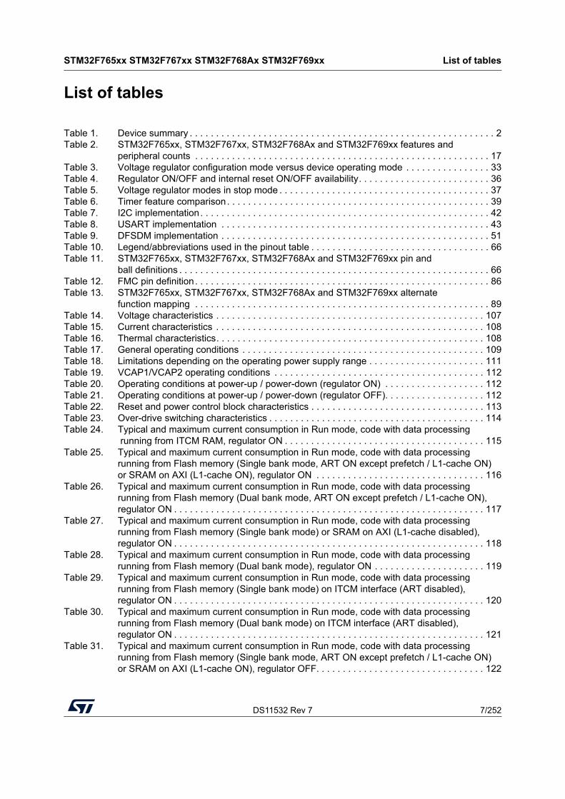
List of tables
Table 1. Device summary . . . . . . . . . . . . . . . . . . . . . . . . . . . . . . . . . . . . . . . . . . . . . . . . . . . . . . . . . . 2Table 2. STM32F765xx, STM32F767xx, STM32F768Ax and STM32F769xx features and
peripheral counts . . . . . . . . . . . . . . . . . . . . . . . . . . . . . . . . . . . . . . . . . . . . . . . . . . . . . . . . 17Table 3. Voltage regulator configuration mode versus device operating mode . . . . . . . . . . . . . . . . 33Table 4. Regulator ON/OFF and internal reset ON/OFF availability. . . . . . . . . . . . . . . . . . . . . . . . . 36Table 5. Voltage regulator modes in stop mode . . . . . . . . . . . . . . . . . . . . . . . . . . . . . . . . . . . . . . . . 37Table 6. Timer feature comparison. . . . . . . . . . . . . . . . . . . . . . . . . . . . . . . . . . . . . . . . . . . . . . . . . . 39Table 7. I2C implementation. . . . . . . . . . . . . . . . . . . . . . . . . . . . . . . . . . . . . . . . . . . . . . . . . . . . . . . 42Table 8. USART implementation . . . . . . . . . . . . . . . . . . . . . . . . . . . . . . . . . . . . . . . . . . . . . . . . . . . 43Table 9. DFSDM implementation . . . . . . . . . . . . . . . . . . . . . . . . . . . . . . . . . . . . . . . . . . . . . . . . . . . 51Table 10. Legend/abbreviations used in the pinout table . . . . . . . . . . . . . . . . . . . . . . . . . . . . . . . . . . 66Table 11. STM32F765xx, STM32F767xx, STM32F768Ax and STM32F769xx pin and
ball definitions . . . . . . . . . . . . . . . . . . . . . . . . . . . . . . . . . . . . . . . . . . . . . . . . . . . . . . . . . . . 66Table 12. FMC pin definition. . . . . . . . . . . . . . . . . . . . . . . . . . . . . . . . . . . . . . . . . . . . . . . . . . . . . . . . 86Table 13. STM32F765xx, STM32F767xx, STM32F768Ax and STM32F769xx alternate
function mapping . . . . . . . . . . . . . . . . . . . . . . . . . . . . . . . . . . . . . . . . . . . . . . . . . . . . . . . . 89Table 14. Voltage characteristics . . . . . . . . . . . . . . . . . . . . . . . . . . . . . . . . . . . . . . . . . . . . . . . . . . . 107Table 15. Current characteristics . . . . . . . . . . . . . . . . . . . . . . . . . . . . . . . . . . . . . . . . . . . . . . . . . . . 108Table 16. Thermal characteristics. . . . . . . . . . . . . . . . . . . . . . . . . . . . . . . . . . . . . . . . . . . . . . . . . . . 108Table 17. General operating conditions . . . . . . . . . . . . . . . . . . . . . . . . . . . . . . . . . . . . . . . . . . . . . . 109Table 18. Limitations depending on the operating power supply range . . . . . . . . . . . . . . . . . . . . . . 111Table 19. VCAP1/VCAP2 operating conditions . . . . . . . . . . . . . . . . . . . . . . . . . . . . . . . . . . . . . . . . 112Table 20. Operating conditions at power-up / power-down (regulator ON) . . . . . . . . . . . . . . . . . . . 112Table 21. Operating conditions at power-up / power-down (regulator OFF). . . . . . . . . . . . . . . . . . . 112Table 22. Reset and power control block characteristics . . . . . . . . . . . . . . . . . . . . . . . . . . . . . . . . . 113Table 23. Over-drive switching characteristics . . . . . . . . . . . . . . . . . . . . . . . . . . . . . . . . . . . . . . . . . 114Table 24. Typical and maximum current consumption in Run mode, code with data processing
running from ITCM RAM, regulator ON . . . . . . . . . . . . . . . . . . . . . . . . . . . . . . . . . . . . . . 115Table 25. Typical and maximum current consumption in Run mode, code with data processing
running from Flash memory (Single bank mode, ART ON except prefetch / L1-cache ON) or SRAM on AXI (L1-cache ON), regulator ON . . . . . . . . . . . . . . . . . . . . . . . . . . . . . . . . 116
Table 26. Typical and maximum current consumption in Run mode, code with data processing running from Flash memory (Dual bank mode, ART ON except prefetch / L1-cache ON), regulator ON . . . . . . . . . . . . . . . . . . . . . . . . . . . . . . . . . . . . . . . . . . . . . . . . . . . . . . . . . . . 117
Table 27. Typical and maximum current consumption in Run mode, code with data processing running from Flash memory (Single bank mode) or SRAM on AXI (L1-cache disabled), regulator ON . . . . . . . . . . . . . . . . . . . . . . . . . . . . . . . . . . . . . . . . . . . . . . . . . . . . . . . . . . . 118
Table 28. Typical and maximum current consumption in Run mode, code with data processing running from Flash memory (Dual bank mode), regulator ON . . . . . . . . . . . . . . . . . . . . . 119
Table 29. Typical and maximum current consumption in Run mode, code with data processing running from Flash memory (Single bank mode) on ITCM interface (ART disabled), regulator ON . . . . . . . . . . . . . . . . . . . . . . . . . . . . . . . . . . . . . . . . . . . . . . . . . . . . . . . . . . . 120
Table 30. Typical and maximum current consumption in Run mode, code with data processing running from Flash memory (Dual bank mode) on ITCM interface (ART disabled), regulator ON . . . . . . . . . . . . . . . . . . . . . . . . . . . . . . . . . . . . . . . . . . . . . . . . . . . . . . . . . . . 121
Table 31. Typical and maximum current consumption in Run mode, code with data processing running from Flash memory (Single bank mode, ART ON except prefetch / L1-cache ON) or SRAM on AXI (L1-cache ON), regulator OFF. . . . . . . . . . . . . . . . . . . . . . . . . . . . . . . . 122
List of tables STM32F765xx STM32F767xx STM32F768Ax STM32F769xx
8/252 DS11532 Rev 7
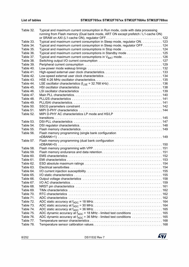
Table 32. Typical and maximum current consumption in Run mode, code with data processing running from Flash memory (Dual bank mode, ART ON except prefetch / L1-cache ON) or SRAM on AXI (L1-cache ON), regulator OFF. . . . . . . . . . . . . . . . . . . . . . . . . . . . . . . . 122
Table 33. Typical and maximum current consumption in Sleep mode, regulator ON. . . . . . . . . . . . 123Table 34. Typical and maximum current consumption in Sleep mode, regulator OFF. . . . . . . . . . . 124Table 35. Typical and maximum current consumptions in Stop mode . . . . . . . . . . . . . . . . . . . . . . . 124Table 36. Typical and maximum current consumptions in Standby mode . . . . . . . . . . . . . . . . . . . . 125Table 37. Typical and maximum current consumptions in VBAT mode. . . . . . . . . . . . . . . . . . . . . . . 126Table 38. Switching output I/O current consumption . . . . . . . . . . . . . . . . . . . . . . . . . . . . . . . . . . . . 127Table 39. Peripheral current consumption . . . . . . . . . . . . . . . . . . . . . . . . . . . . . . . . . . . . . . . . . . . . 129Table 40. Low-power mode wakeup timings . . . . . . . . . . . . . . . . . . . . . . . . . . . . . . . . . . . . . . . . . . 132Table 41. High-speed external user clock characteristics. . . . . . . . . . . . . . . . . . . . . . . . . . . . . . . . . 133Table 42. Low-speed external user clock characteristics . . . . . . . . . . . . . . . . . . . . . . . . . . . . . . . . . 134Table 43. HSE 4-26 MHz oscillator characteristics. . . . . . . . . . . . . . . . . . . . . . . . . . . . . . . . . . . . . . 135Table 44. LSE oscillator characteristics (fLSE = 32.768 kHz) . . . . . . . . . . . . . . . . . . . . . . . . . . . . . . 136Table 45. HSI oscillator characteristics . . . . . . . . . . . . . . . . . . . . . . . . . . . . . . . . . . . . . . . . . . . . . . 138Table 46. LSI oscillator characteristics . . . . . . . . . . . . . . . . . . . . . . . . . . . . . . . . . . . . . . . . . . . . . . 139Table 47. Main PLL characteristics. . . . . . . . . . . . . . . . . . . . . . . . . . . . . . . . . . . . . . . . . . . . . . . . . . 140Table 48. PLLI2S characteristics . . . . . . . . . . . . . . . . . . . . . . . . . . . . . . . . . . . . . . . . . . . . . . . . . . . 141Table 49. PLLISAI characteristics. . . . . . . . . . . . . . . . . . . . . . . . . . . . . . . . . . . . . . . . . . . . . . . . . . . 141Table 50. SSCG parameters constraint . . . . . . . . . . . . . . . . . . . . . . . . . . . . . . . . . . . . . . . . . . . . . . 142Table 51. MIPI D-PHY characteristics . . . . . . . . . . . . . . . . . . . . . . . . . . . . . . . . . . . . . . . . . . . . . . . 144Table 52. MIPI D-PHY AC characteristics LP mode and HS/LP
transitions . . . . . . . . . . . . . . . . . . . . . . . . . . . . . . . . . . . . . . . . . . . . . . . . . . . . . . . . . . . . . 145Table 53. DSI-PLL characteristics . . . . . . . . . . . . . . . . . . . . . . . . . . . . . . . . . . . . . . . . . . . . . . . . . . 147Table 54. DSI regulator characteristics. . . . . . . . . . . . . . . . . . . . . . . . . . . . . . . . . . . . . . . . . . . . . . . 148Table 55. Flash memory characteristics . . . . . . . . . . . . . . . . . . . . . . . . . . . . . . . . . . . . . . . . . . . . . . 149Table 56. Flash memory programming (single bank configuration
nDBANK=1) . . . . . . . . . . . . . . . . . . . . . . . . . . . . . . . . . . . . . . . . . . . . . . . . . . . . . . . . . . . 149Table 57. Flash memory programming (dual bank configuration
nDBANK=0) . . . . . . . . . . . . . . . . . . . . . . . . . . . . . . . . . . . . . . . . . . . . . . . . . . . . . . . . . . . 150Table 58. Flash memory programming with VPP . . . . . . . . . . . . . . . . . . . . . . . . . . . . . . . . . . . . . . . 151Table 59. Flash memory endurance and data retention . . . . . . . . . . . . . . . . . . . . . . . . . . . . . . . . . . 151Table 60. EMS characteristics . . . . . . . . . . . . . . . . . . . . . . . . . . . . . . . . . . . . . . . . . . . . . . . . . . . . . 152Table 61. EMI characteristics . . . . . . . . . . . . . . . . . . . . . . . . . . . . . . . . . . . . . . . . . . . . . . . . . . . . . . 153Table 62. ESD absolute maximum ratings . . . . . . . . . . . . . . . . . . . . . . . . . . . . . . . . . . . . . . . . . . . . 154Table 63. Electrical sensitivities . . . . . . . . . . . . . . . . . . . . . . . . . . . . . . . . . . . . . . . . . . . . . . . . . . . . 154Table 64. I/O current injection susceptibility . . . . . . . . . . . . . . . . . . . . . . . . . . . . . . . . . . . . . . . . . . . 155Table 65. I/O static characteristics . . . . . . . . . . . . . . . . . . . . . . . . . . . . . . . . . . . . . . . . . . . . . . . . . . 155Table 66. Output voltage characteristics . . . . . . . . . . . . . . . . . . . . . . . . . . . . . . . . . . . . . . . . . . . . . 158Table 67. I/O AC characteristics . . . . . . . . . . . . . . . . . . . . . . . . . . . . . . . . . . . . . . . . . . . . . . . . . . . . 159Table 68. NRST pin characteristics . . . . . . . . . . . . . . . . . . . . . . . . . . . . . . . . . . . . . . . . . . . . . . . . . 161Table 69. TIMx characteristics . . . . . . . . . . . . . . . . . . . . . . . . . . . . . . . . . . . . . . . . . . . . . . . . . . . . . 162Table 70. RTC characteristics . . . . . . . . . . . . . . . . . . . . . . . . . . . . . . . . . . . . . . . . . . . . . . . . . . . . . 162Table 71. ADC characteristics . . . . . . . . . . . . . . . . . . . . . . . . . . . . . . . . . . . . . . . . . . . . . . . . . . . . . 162Table 72. ADC static accuracy at fADC = 18 MHz. . . . . . . . . . . . . . . . . . . . . . . . . . . . . . . . . . . . . . . 164Table 73. ADC static accuracy at fADC = 30 MHz. . . . . . . . . . . . . . . . . . . . . . . . . . . . . . . . . . . . . . . 164Table 74. ADC static accuracy at fADC = 36 MHz. . . . . . . . . . . . . . . . . . . . . . . . . . . . . . . . . . . . . . . 165Table 75. ADC dynamic accuracy at fADC = 18 MHz - limited test conditions . . . . . . . . . . . . . . . . . 165Table 76. ADC dynamic accuracy at fADC = 36 MHz - limited test conditions . . . . . . . . . . . . . . . . . 165Table 77. Temperature sensor characteristics . . . . . . . . . . . . . . . . . . . . . . . . . . . . . . . . . . . . . . . . . 168Table 78. Temperature sensor calibration values. . . . . . . . . . . . . . . . . . . . . . . . . . . . . . . . . . . . . . . 168
DS11532 Rev 7 9/252
STM32F765xx STM32F767xx STM32F768Ax STM32F769xx List of tables
10
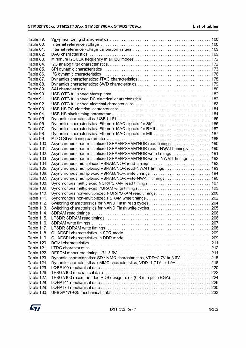
Table 79. VBAT monitoring characteristics . . . . . . . . . . . . . . . . . . . . . . . . . . . . . . . . . . . . . . . . . . . . 168Table 80. internal reference voltage . . . . . . . . . . . . . . . . . . . . . . . . . . . . . . . . . . . . . . . . . . . . . . . . 168Table 81. Internal reference voltage calibration values . . . . . . . . . . . . . . . . . . . . . . . . . . . . . . . . . . 169Table 82. DAC characteristics . . . . . . . . . . . . . . . . . . . . . . . . . . . . . . . . . . . . . . . . . . . . . . . . . . . . . 169Table 83. Minimum I2CCLK frequency in all I2C modes . . . . . . . . . . . . . . . . . . . . . . . . . . . . . . . . . 172Table 84. I2C analog filter characteristics. . . . . . . . . . . . . . . . . . . . . . . . . . . . . . . . . . . . . . . . . . . . . 172Table 85. SPI dynamic characteristics . . . . . . . . . . . . . . . . . . . . . . . . . . . . . . . . . . . . . . . . . . . . . . . 173Table 86. I2S dynamic characteristics . . . . . . . . . . . . . . . . . . . . . . . . . . . . . . . . . . . . . . . . . . . . . . . 176Table 87. Dynamics characteristics: JTAG characteristics . . . . . . . . . . . . . . . . . . . . . . . . . . . . . . . . 178Table 88. Dynamics characteristics: SWD characteristics . . . . . . . . . . . . . . . . . . . . . . . . . . . . . . . . 179Table 89. SAI characteristics . . . . . . . . . . . . . . . . . . . . . . . . . . . . . . . . . . . . . . . . . . . . . . . . . . . . . . 180Table 90. USB OTG full speed startup time . . . . . . . . . . . . . . . . . . . . . . . . . . . . . . . . . . . . . . . . . . . 182Table 91. USB OTG full speed DC electrical characteristics . . . . . . . . . . . . . . . . . . . . . . . . . . . . . . 182Table 92. USB OTG full speed electrical characteristics . . . . . . . . . . . . . . . . . . . . . . . . . . . . . . . . . 183Table 93. USB HS DC electrical characteristics . . . . . . . . . . . . . . . . . . . . . . . . . . . . . . . . . . . . . . . . 184Table 94. USB HS clock timing parameters . . . . . . . . . . . . . . . . . . . . . . . . . . . . . . . . . . . . . . . . . . . 184Table 95. Dynamic characteristics: USB ULPI . . . . . . . . . . . . . . . . . . . . . . . . . . . . . . . . . . . . . . . . . 185Table 96. Dynamics characteristics: Ethernet MAC signals for SMI. . . . . . . . . . . . . . . . . . . . . . . . . 186Table 97. Dynamics characteristics: Ethernet MAC signals for RMII . . . . . . . . . . . . . . . . . . . . . . . . 187Table 98. Dynamics characteristics: Ethernet MAC signals for MII . . . . . . . . . . . . . . . . . . . . . . . . . 187Table 99. MDIO Slave timing parameters. . . . . . . . . . . . . . . . . . . . . . . . . . . . . . . . . . . . . . . . . . . . . 188Table 100. Asynchronous non-multiplexed SRAM/PSRAM/NOR read timings . . . . . . . . . . . . . . . . . 190Table 101. Asynchronous non-multiplexed SRAM/PSRAM/NOR read - NWAIT timings . . . . . . . . . . 190Table 102. Asynchronous non-multiplexed SRAM/PSRAM/NOR write timings . . . . . . . . . . . . . . . . . 191Table 103. Asynchronous non-multiplexed SRAM/PSRAM/NOR write - NWAIT timings. . . . . . . . . . 192Table 104. Asynchronous multiplexed PSRAM/NOR read timings. . . . . . . . . . . . . . . . . . . . . . . . . . . 193Table 105. Asynchronous multiplexed PSRAM/NOR read-NWAIT timings . . . . . . . . . . . . . . . . . . . . 193Table 106. Asynchronous multiplexed PSRAM/NOR write timings . . . . . . . . . . . . . . . . . . . . . . . . . . 194Table 107. Asynchronous multiplexed PSRAM/NOR write-NWAIT timings . . . . . . . . . . . . . . . . . . . . 195Table 108. Synchronous multiplexed NOR/PSRAM read timings . . . . . . . . . . . . . . . . . . . . . . . . . . . 197Table 109. Synchronous multiplexed PSRAM write timings. . . . . . . . . . . . . . . . . . . . . . . . . . . . . . . . 199Table 110. Synchronous non-multiplexed NOR/PSRAM read timings . . . . . . . . . . . . . . . . . . . . . . . . 200Table 111. Synchronous non-multiplexed PSRAM write timings . . . . . . . . . . . . . . . . . . . . . . . . . . . . 202Table 112. Switching characteristics for NAND Flash read cycles . . . . . . . . . . . . . . . . . . . . . . . . . . . 204Table 113. Switching characteristics for NAND Flash write cycles. . . . . . . . . . . . . . . . . . . . . . . . . . . 205Table 114. SDRAM read timings . . . . . . . . . . . . . . . . . . . . . . . . . . . . . . . . . . . . . . . . . . . . . . . . . . . . 206Table 115. LPSDR SDRAM read timings . . . . . . . . . . . . . . . . . . . . . . . . . . . . . . . . . . . . . . . . . . . . . . 206Table 116. SDRAM write timings . . . . . . . . . . . . . . . . . . . . . . . . . . . . . . . . . . . . . . . . . . . . . . . . . . . . 207Table 117. LPSDR SDRAM write timings. . . . . . . . . . . . . . . . . . . . . . . . . . . . . . . . . . . . . . . . . . . . . . 208Table 118. QUADSPI characteristics in SDR mode . . . . . . . . . . . . . . . . . . . . . . . . . . . . . . . . . . . . . . 209Table 119. QUADSPI characteristics in DDR mode . . . . . . . . . . . . . . . . . . . . . . . . . . . . . . . . . . . . . . 209Table 120. DCMI characteristics. . . . . . . . . . . . . . . . . . . . . . . . . . . . . . . . . . . . . . . . . . . . . . . . . . . . . 211Table 121. LTDC characteristics . . . . . . . . . . . . . . . . . . . . . . . . . . . . . . . . . . . . . . . . . . . . . . . . . . . . 212Table 122. DFSDM measured timing 1.71-3.6V. . . . . . . . . . . . . . . . . . . . . . . . . . . . . . . . . . . . . . . . . 214Table 123. Dynamic characteristics: SD / MMC characteristics, VDD=2.7V to 3.6V . . . . . . . . . . . . . 218Table 124. Dynamic characteristics: eMMC characteristics, VDD=1.71V to 1.9V . . . . . . . . . . . . . . . 218Table 125. LQPF100 mechanical data . . . . . . . . . . . . . . . . . . . . . . . . . . . . . . . . . . . . . . . . . . . . . . . . 220Table 126. TFBGA100 mechanical data. . . . . . . . . . . . . . . . . . . . . . . . . . . . . . . . . . . . . . . . . . . . . . . 222Table 127. TFBGA100 recommended PCB design rules (0.8 mm pitch BGA). . . . . . . . . . . . . . . . . . 224Table 128. LQFP144 mechanical data . . . . . . . . . . . . . . . . . . . . . . . . . . . . . . . . . . . . . . . . . . . . . . . . 226Table 129. LQFP176 mechanical data . . . . . . . . . . . . . . . . . . . . . . . . . . . . . . . . . . . . . . . . . . . . . . . . 230Table 130. UFBGA176+25 mechanical data . . . . . . . . . . . . . . . . . . . . . . . . . . . . . . . . . . . . . . . . . . . 233
List of tables STM32F765xx STM32F767xx STM32F768Ax STM32F769xx
10/252 DS11532 Rev 7
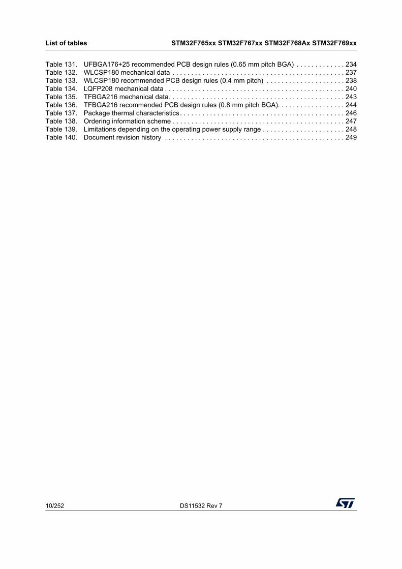
Table 131. UFBGA176+25 recommended PCB design rules (0.65 mm pitch BGA) . . . . . . . . . . . . . 234Table 132. WLCSP180 mechanical data . . . . . . . . . . . . . . . . . . . . . . . . . . . . . . . . . . . . . . . . . . . . . . 237Table 133. WLCSP180 recommended PCB design rules (0.4 mm pitch) . . . . . . . . . . . . . . . . . . . . . 238Table 134. LQFP208 mechanical data . . . . . . . . . . . . . . . . . . . . . . . . . . . . . . . . . . . . . . . . . . . . . . . . 240Table 135. TFBGA216 mechanical data. . . . . . . . . . . . . . . . . . . . . . . . . . . . . . . . . . . . . . . . . . . . . . . 243Table 136. TFBGA216 recommended PCB design rules (0.8 mm pitch BGA). . . . . . . . . . . . . . . . . . 244Table 137. Package thermal characteristics . . . . . . . . . . . . . . . . . . . . . . . . . . . . . . . . . . . . . . . . . . . . 246Table 138. Ordering information scheme . . . . . . . . . . . . . . . . . . . . . . . . . . . . . . . . . . . . . . . . . . . . . . 247Table 139. Limitations depending on the operating power supply range . . . . . . . . . . . . . . . . . . . . . . 248Table 140. Document revision history . . . . . . . . . . . . . . . . . . . . . . . . . . . . . . . . . . . . . . . . . . . . . . . . 249
DS11532 Rev 7 11/252
STM32F765xx STM32F767xx STM32F768Ax STM32F769xx List of figures
13
List of figures
Figure 1. Compatible board design for LQFP100 package . . . . . . . . . . . . . . . . . . . . . . . . . . . . . . . 19Figure 2. STM32F765xx, STM32F767xx, STM32F768Ax and STM32F769xx block diagram . . . . 20Figure 3. STM32F765xx, STM32F767xx, STM32F768Ax and STM32F769xx AXI-AHB
bus matrix architecture(1) . . . . . . . . . . . . . . . . . . . . . . . . . . . . . . . . . . . . . . . . . . . . . . . . . . 23Figure 4. VDDUSB connected to VDD power supply . . . . . . . . . . . . . . . . . . . . . . . . . . . . . . . . . . . . 29Figure 5. VDDUSB connected to external power supply . . . . . . . . . . . . . . . . . . . . . . . . . . . . . . . . . . 30Figure 6. Power supply supervisor interconnection with internal reset OFF . . . . . . . . . . . . . . . . . . . 31Figure 7. PDR_ON control with internal reset OFF . . . . . . . . . . . . . . . . . . . . . . . . . . . . . . . . . . . . . . 32Figure 8. Regulator OFF . . . . . . . . . . . . . . . . . . . . . . . . . . . . . . . . . . . . . . . . . . . . . . . . . . . . . . . . . . 34Figure 9. Startup in regulator OFF: slow VDD slope
- power-down reset risen after VCAP_1,VCAP_2 stabilization . . . . . . . . . . . . . . . . . . . . . . . . 35Figure 10. Startup in regulator OFF mode: fast VDD slope
- power-down reset risen before VCAP_1,VCAP_2 stabilization. . . . . . . . . . . . . . . . . . . . . . . 35Figure 11. STM32F76xxx LQFP100 pinout . . . . . . . . . . . . . . . . . . . . . . . . . . . . . . . . . . . . . . . . . . . . . 55Figure 12. STM32F76xxx TFBGA100 pinout . . . . . . . . . . . . . . . . . . . . . . . . . . . . . . . . . . . . . . . . . . . . 56Figure 13. STM32F76xxx LQFP144 pinout . . . . . . . . . . . . . . . . . . . . . . . . . . . . . . . . . . . . . . . . . . . . . 57Figure 14. STM32F76xxx LQFP176 pinout . . . . . . . . . . . . . . . . . . . . . . . . . . . . . . . . . . . . . . . . . . . . . 58Figure 15. STM32F769xx LQFP176 pinout . . . . . . . . . . . . . . . . . . . . . . . . . . . . . . . . . . . . . . . . . . . . . 59Figure 16. STM32F76xxx UFBGA176 ballout . . . . . . . . . . . . . . . . . . . . . . . . . . . . . . . . . . . . . . . . . . . 60Figure 17. STM32F769Ax/STM32F768Ax WLCSP180 ballout . . . . . . . . . . . . . . . . . . . . . . . . . . . . . . 61Figure 18. STM32F76xxx LQFP208 pinout . . . . . . . . . . . . . . . . . . . . . . . . . . . . . . . . . . . . . . . . . . . . . 62Figure 19. STM32F769xx LQFP208 pinout . . . . . . . . . . . . . . . . . . . . . . . . . . . . . . . . . . . . . . . . . . . . . 63Figure 20. STM32F76xxx TFBGA216 ballout . . . . . . . . . . . . . . . . . . . . . . . . . . . . . . . . . . . . . . . . . . . 64Figure 21. STM32F769xx TFBGA216 ballout . . . . . . . . . . . . . . . . . . . . . . . . . . . . . . . . . . . . . . . . . . . 65Figure 22. Pin loading conditions. . . . . . . . . . . . . . . . . . . . . . . . . . . . . . . . . . . . . . . . . . . . . . . . . . . . 104Figure 23. Pin input voltage . . . . . . . . . . . . . . . . . . . . . . . . . . . . . . . . . . . . . . . . . . . . . . . . . . . . . . . . 104Figure 24. STM32F769xx/STM32F779xx power supply scheme . . . . . . . . . . . . . . . . . . . . . . . . . . . 105Figure 25. STM32F765xx/STM32F767xx/STM32F777xx power supply scheme . . . . . . . . . . . . . . . 106Figure 26. Current consumption measurement scheme . . . . . . . . . . . . . . . . . . . . . . . . . . . . . . . . . . 107Figure 27. External capacitor CEXT . . . . . . . . . . . . . . . . . . . . . . . . . . . . . . . . . . . . . . . . . . . . . . . . . . 111Figure 28. High-speed external clock source AC timing diagram . . . . . . . . . . . . . . . . . . . . . . . . . . . 134Figure 29. Low-speed external clock source AC timing diagram. . . . . . . . . . . . . . . . . . . . . . . . . . . . 135Figure 30. Typical application with an 8 MHz crystal . . . . . . . . . . . . . . . . . . . . . . . . . . . . . . . . . . . . . 136Figure 31. Typical application with a 32.768 kHz crystal . . . . . . . . . . . . . . . . . . . . . . . . . . . . . . . . . . 137Figure 32. ACCHSI versus temperature . . . . . . . . . . . . . . . . . . . . . . . . . . . . . . . . . . . . . . . . . . . . . . 138Figure 33. LSI deviation versus temperature . . . . . . . . . . . . . . . . . . . . . . . . . . . . . . . . . . . . . . . . . . . 139Figure 34. PLL output clock waveforms in center spread mode . . . . . . . . . . . . . . . . . . . . . . . . . . . . 143Figure 35. PLL output clock waveforms in down spread mode . . . . . . . . . . . . . . . . . . . . . . . . . . . . . 144Figure 36. MIPI D-PHY HS/LP clock lane transition timing diagram . . . . . . . . . . . . . . . . . . . . . . . . . 147Figure 37. MIPI D-PHY HS/LP data lane transition timing diagram. . . . . . . . . . . . . . . . . . . . . . . . . . 147Figure 38. FT I/O input characteristics. . . . . . . . . . . . . . . . . . . . . . . . . . . . . . . . . . . . . . . . . . . . . . . . 157Figure 39. I/O AC characteristics definition . . . . . . . . . . . . . . . . . . . . . . . . . . . . . . . . . . . . . . . . . . . . 160Figure 40. Recommended NRST pin protection . . . . . . . . . . . . . . . . . . . . . . . . . . . . . . . . . . . . . . . . 161Figure 41. ADC accuracy characteristics . . . . . . . . . . . . . . . . . . . . . . . . . . . . . . . . . . . . . . . . . . . . . . 166Figure 42. Typical connection diagram using the ADC . . . . . . . . . . . . . . . . . . . . . . . . . . . . . . . . . . . 166Figure 43. Power supply and reference decoupling (VREF+ not connected to VDDA). . . . . . . . . . . . . 167Figure 44. Power supply and reference decoupling (VREF+ connected to VDDA). . . . . . . . . . . . . . . . 167Figure 45. 12-bit buffered /non-buffered DAC . . . . . . . . . . . . . . . . . . . . . . . . . . . . . . . . . . . . . . . . . . 171
List of figures STM32F765xx STM32F767xx STM32F768Ax STM32F769xx
12/252 DS11532 Rev 7
Figure 46. SPI timing diagram - slave mode and CPHA = 0 . . . . . . . . . . . . . . . . . . . . . . . . . . . . . . . 174Figure 47. SPI timing diagram - slave mode and CPHA = 1(1) . . . . . . . . . . . . . . . . . . . . . . . . . . . . . 175Figure 48. SPI timing diagram - master mode(1) . . . . . . . . . . . . . . . . . . . . . . . . . . . . . . . . . . . . . . . . 175Figure 49. I2S slave timing diagram (Philips protocol)(1) . . . . . . . . . . . . . . . . . . . . . . . . . . . . . . . . . . 177Figure 50. I2S master timing diagram (Philips protocol)(1) . . . . . . . . . . . . . . . . . . . . . . . . . . . . . . . . . 177Figure 51. JTAG timing diagram . . . . . . . . . . . . . . . . . . . . . . . . . . . . . . . . . . . . . . . . . . . . . . . . . . . . 179Figure 52. SWD timing diagram. . . . . . . . . . . . . . . . . . . . . . . . . . . . . . . . . . . . . . . . . . . . . . . . . . . . . 180Figure 53. SAI master timing waveforms . . . . . . . . . . . . . . . . . . . . . . . . . . . . . . . . . . . . . . . . . . . . . . 181Figure 54. SAI slave timing waveforms . . . . . . . . . . . . . . . . . . . . . . . . . . . . . . . . . . . . . . . . . . . . . . . 182Figure 55. USB OTG full speed timings: definition of data signal rise and fall time. . . . . . . . . . . . . . 183Figure 56. ULPI timing diagram . . . . . . . . . . . . . . . . . . . . . . . . . . . . . . . . . . . . . . . . . . . . . . . . . . . . . 185Figure 57. Ethernet SMI timing diagram . . . . . . . . . . . . . . . . . . . . . . . . . . . . . . . . . . . . . . . . . . . . . . 186Figure 58. Ethernet RMII timing diagram . . . . . . . . . . . . . . . . . . . . . . . . . . . . . . . . . . . . . . . . . . . . . . 186Figure 59. Ethernet MII timing diagram . . . . . . . . . . . . . . . . . . . . . . . . . . . . . . . . . . . . . . . . . . . . . . . 187Figure 60. MDIO Slave timing diagram . . . . . . . . . . . . . . . . . . . . . . . . . . . . . . . . . . . . . . . . . . . . . . . 188Figure 61. Asynchronous non-multiplexed SRAM/PSRAM/NOR read waveforms . . . . . . . . . . . . . . 189Figure 62. Asynchronous non-multiplexed SRAM/PSRAM/NOR write waveforms . . . . . . . . . . . . . . 191Figure 63. Asynchronous multiplexed PSRAM/NOR read waveforms. . . . . . . . . . . . . . . . . . . . . . . . 192Figure 64. Asynchronous multiplexed PSRAM/NOR write waveforms . . . . . . . . . . . . . . . . . . . . . . . 194Figure 65. Synchronous multiplexed NOR/PSRAM read timings . . . . . . . . . . . . . . . . . . . . . . . . . . . 196Figure 66. Synchronous multiplexed PSRAM write timings. . . . . . . . . . . . . . . . . . . . . . . . . . . . . . . . 198Figure 67. Synchronous non-multiplexed NOR/PSRAM read timings . . . . . . . . . . . . . . . . . . . . . . . . 200Figure 68. Synchronous non-multiplexed PSRAM write timings . . . . . . . . . . . . . . . . . . . . . . . . . . . . 201Figure 69. NAND controller waveforms for read access . . . . . . . . . . . . . . . . . . . . . . . . . . . . . . . . . . 203Figure 70. NAND controller waveforms for write access . . . . . . . . . . . . . . . . . . . . . . . . . . . . . . . . . . 203Figure 71. NAND controller waveforms for common memory read access . . . . . . . . . . . . . . . . . . . . 204Figure 72. NAND controller waveforms for common memory write access. . . . . . . . . . . . . . . . . . . . 204Figure 73. SDRAM read access waveforms (CL = 1) . . . . . . . . . . . . . . . . . . . . . . . . . . . . . . . . . . . . 205Figure 74. SDRAM write access waveforms . . . . . . . . . . . . . . . . . . . . . . . . . . . . . . . . . . . . . . . . . . . 207Figure 75. Quad-SPI timing diagram - SDR mode. . . . . . . . . . . . . . . . . . . . . . . . . . . . . . . . . . . . . . . 210Figure 76. Quad-SPI timing diagram - DDR mode . . . . . . . . . . . . . . . . . . . . . . . . . . . . . . . . . . . . . . 210Figure 77. DCMI timing diagram . . . . . . . . . . . . . . . . . . . . . . . . . . . . . . . . . . . . . . . . . . . . . . . . . . . . 211Figure 78. LCD-TFT horizontal timing diagram . . . . . . . . . . . . . . . . . . . . . . . . . . . . . . . . . . . . . . . . . 213Figure 79. LCD-TFT vertical timing diagram . . . . . . . . . . . . . . . . . . . . . . . . . . . . . . . . . . . . . . . . . . . 213Figure 80. Channel transceiver timing diagrams . . . . . . . . . . . . . . . . . . . . . . . . . . . . . . . . . . . . . . . . 216Figure 81. SDIO high-speed mode . . . . . . . . . . . . . . . . . . . . . . . . . . . . . . . . . . . . . . . . . . . . . . . . . . 217Figure 82. SD default mode . . . . . . . . . . . . . . . . . . . . . . . . . . . . . . . . . . . . . . . . . . . . . . . . . . . . . . . . 217Figure 83. LQFP100 outline. . . . . . . . . . . . . . . . . . . . . . . . . . . . . . . . . . . . . . . . . . . . . . . . . . . . . . . . 219Figure 84. LQFP100 recommended footprint . . . . . . . . . . . . . . . . . . . . . . . . . . . . . . . . . . . . . . . . . . 220Figure 85. LQFP100 top view example . . . . . . . . . . . . . . . . . . . . . . . . . . . . . . . . . . . . . . . . . . . . . . 221Figure 86. TFBGA100 outline . . . . . . . . . . . . . . . . . . . . . . . . . . . . . . . . . . . . . . . . . . . . . . . . . . . . . . 222Figure 87. TFBGA100 recommended footprint . . . . . . . . . . . . . . . . . . . . . . . . . . . . . . . . . . . . . . . . . 223Figure 88. TFBGA100 top view example . . . . . . . . . . . . . . . . . . . . . . . . . . . . . . . . . . . . . . . . . . . . . 224Figure 89. LQFP144 outline. . . . . . . . . . . . . . . . . . . . . . . . . . . . . . . . . . . . . . . . . . . . . . . . . . . . . . . . 225Figure 90. LQFP144 recommended footprint . . . . . . . . . . . . . . . . . . . . . . . . . . . . . . . . . . . . . . . . . . 227Figure 91. LQFP144 top view example . . . . . . . . . . . . . . . . . . . . . . . . . . . . . . . . . . . . . . . . . . . . . . 228Figure 92. LQFP176 outline. . . . . . . . . . . . . . . . . . . . . . . . . . . . . . . . . . . . . . . . . . . . . . . . . . . . . . . . 229Figure 93. LQFP176 recommended footprint . . . . . . . . . . . . . . . . . . . . . . . . . . . . . . . . . . . . . . . . . . 231Figure 94. LQFP176 top view example . . . . . . . . . . . . . . . . . . . . . . . . . . . . . . . . . . . . . . . . . . . . . . 232Figure 95. UFBGA176+25 outline . . . . . . . . . . . . . . . . . . . . . . . . . . . . . . . . . . . . . . . . . . . . . . . . . . . 233Figure 96. UFBGA176+25 recommended footprint . . . . . . . . . . . . . . . . . . . . . . . . . . . . . . . . . . . . . . 234Figure 97. UFBGA176+25 top view example . . . . . . . . . . . . . . . . . . . . . . . . . . . . . . . . . . . . . . . . . . 235
DS11532 Rev 7 13/252
STM32F765xx STM32F767xx STM32F768Ax STM32F769xx List of figures
13
Figure 98. WLCSP180 outline . . . . . . . . . . . . . . . . . . . . . . . . . . . . . . . . . . . . . . . . . . . . . . . . . . . . . . 236Figure 99. WLCSP180 recommended footprint . . . . . . . . . . . . . . . . . . . . . . . . . . . . . . . . . . . . . . . . . 237Figure 100. WLCSP180 top view example . . . . . . . . . . . . . . . . . . . . . . . . . . . . . . . . . . . . . . . . . . . . 238Figure 101. LQFP208 outline. . . . . . . . . . . . . . . . . . . . . . . . . . . . . . . . . . . . . . . . . . . . . . . . . . . . . . . . 239Figure 102. LQFP208 recommended footprint . . . . . . . . . . . . . . . . . . . . . . . . . . . . . . . . . . . . . . . . . . 241Figure 103. LQFP208 top view example . . . . . . . . . . . . . . . . . . . . . . . . . . . . . . . . . . . . . . . . . . . . . . 242Figure 104. TFBGA216 outline . . . . . . . . . . . . . . . . . . . . . . . . . . . . . . . . . . . . . . . . . . . . . . . . . . . . . . 243Figure 105. TFBGA216 recommended footprint . . . . . . . . . . . . . . . . . . . . . . . . . . . . . . . . . . . . . . . . . 244Figure 106. TFBGA216 top view example . . . . . . . . . . . . . . . . . . . . . . . . . . . . . . . . . . . . . . . . . . . . . 245
Introduction STM32F765xx STM32F767xx STM32F768Ax STM32F769xx
14/252 DS11532 Rev 7
1 Introduction
This document provides information on STM32F765xx, STM32F767xx, STM32F768Ax and STM32F769xx microcontrollers, such as description, functional overview, pin assignment and definition, electrical characteristics, packaging, and ordering information.
This document should be read in conjunction with the STM32F765xx, STM32F767xx, STM32F768Ax and STM32F769xx reference manual (RM0410), available from the STMicroelectronics website www.st.com.
For information on the Arm®(a) Cortex®-M7 core, please refer to the Cortex®-M7 Technical Reference Manual, available from the http://www.arm.com website.
a. Arm is a registered trademark of Arm Limited (or its subsidiaries) in the US and/or elsewhere.
DS11532 Rev 7 15/252
STM32F765xx STM32F767xx STM32F768Ax STM32F769xx Description
54
2 Description
The STM32F765xx, STM32F767xx, STM32F768Ax and STM32F769xx devices are based on the high-performance Arm® Cortex®-M7 32-bit RISC core operating at up to 216 MHz frequency. The Cortex®-M7 core features a floating point unit (FPU) which supports Arm® double-precision and single-precision data-processing instructions and data types. It also implements a full set of DSP instructions and a memory protection unit (MPU) which enhances the application security.
The STM32F765xx, STM32F767xx, STM32F768Ax and STM32F769xx devices incorporate high-speed embedded memories with a Flash memory up to 2 Mbytes, 512 Kbytes of SRAM (including 128 Kbytes of Data TCM RAM for critical real-time data), 16 Kbytes of instruction TCM RAM (for critical real-time routines), 4 Kbytes of backup SRAM available in the lowest power modes, and an extensive range of enhanced I/Os and peripherals connected to two APB buses, two AHB buses, a 32-bit multi-AHB bus matrix and a multi layer AXI interconnect supporting internal and external memories access.
All the devices offer three 12-bit ADCs, two DACs, a low-power RTC, twelve general-purpose 16-bit timers including two PWM timers for motor control, two general-purpose 32-bit timers, a true random number generator (RNG). They also feature standard and advanced communication interfaces:
- Up to four I2Cs
- Six SPIs, three I2Ss in half-duplex mode. To achieve audio class accuracy, the I2S peripherals can be clocked via a dedicated internal audio PLL or via an external clock to allow synchronization.
- Four USARTs plus four UARTs
- An USB OTG full-speed and a USB OTG high-speed with full-speed capability (with the ULPI)
- Three CANs
- Two SAI serial audio interfaces
- Two SDMMC host interfaces
- Ethernet and camera interfaces
- LCD-TFT display controller
- Chrom-ART Accelerator
- SPDIFRX interface
- HDMI-CEC
Advanced peripherals include two SDMMC interfaces, a flexible memory control (FMC) interface, a Quad-SPI Flash memory interface, a camera interface for CMOS sensors.
The STM32F765xx, STM32F767xx, STM32F768Ax and STM32F769xx devices operate in the –40 to +105 °C temperature range from a 1.7 to 3.6 V power supply. Dedicated supply inputs for USB (OTG_FS and OTG_HS) and SDMMC2 (clock, command and 4-bit data) are available on all the packages except LQFP100 for a greater power supply choice.
The supply voltage can drop to 1.7 V with the use of an external power supply supervisor. A comprehensive set of power-saving mode allows the design of low-power applications.
Description STM32F765xx STM32F767xx STM32F768Ax STM32F769xx
16/252 DS11532 Rev 7
The STM32F765xx, STM32F767xx, STM32F768Ax and STM32F769xx devices offer devices in 11 packages ranging from 100 pins to 216 pins. The set of included peripherals changes with the device chosen.
These features make the STM32F765xx, STM32F767xx, STM32F768Ax and STM32F769xx microcontrollers suitable for a wide range of applications:
- Motor drive and application control
- Medical equipment
- Industrial applications: PLC, inverters, circuit breakers
- Printers, and scanners
- Alarm systems, video intercom, and HVAC
- Home audio appliances
- Mobile applications, Internet of Things
- Wearable devices: smartwatches
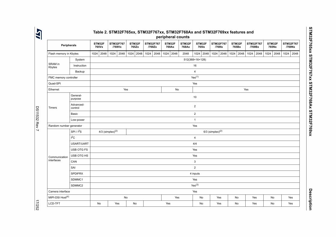
The following table lists the peripherals available on each part number.
ST
M3
2F7
65xx
ST
M3
2F7
67xx
ST
M3
2F7
68A
x S
TM
32F
769
xxD
esc
riptio
n
DS
11532 R
ev 717/252
Table 2. STM32F765xx, STM32F767xx, STM32F768Ax and STM32F769xx features andperipheral counts
PeripheralsSTM32F765Vx
STM32F767/769Vx
STM32F765Zx
STM32F767/769Zx
STM32F769Ax
STM32F768Ax
STM32F765Ix
STM32F767/769Ix
STM32F765Bx
STM32F767/769Bx
STM32F765Nx
STM32F767/769Nx
Flash memory in Kbytes 1024 2048 1024 2048 1024 2048 1024 2048 1024 2048 2048 1024 2048 1024 2048 1024 2048 1024 2048 1024 2048 1024 2048
SRAM in Kbytes
System 512(368+16+128)
Instruction 16
Backup 4
FMC memory controller Yes(1)
Quad-SPI Yes
Ethernet Yes No Yes
Timers
General-purpose
10
Advanced-control
2
Basic 2
Low-power 1
Random number generator Yes
Communication interfaces
SPI / I2S 4/3 (simplex)(2) 6/3 (simplex)(2)
I2C 4
USART/UART 4/4
USB OTG FS Yes
USB OTG HS Yes
CAN 3
SAI 2
SPDIFRX 4 inputs
SDMMC1 Yes
SDMMC2 Yes(3)
Camera interface Yes
MIPI-DSI Host(4) No Yes No Yes No Yes No Yes
LCD-TFT No Yes No Yes No Yes No Yes No Yes
Des
criptio
nS
TM
32F
765
xx S
TM
32F
767
xx S
TM
32F
768
Ax
ST
M32
F76
9xx
18/2
52D
S115
32 Rev 7
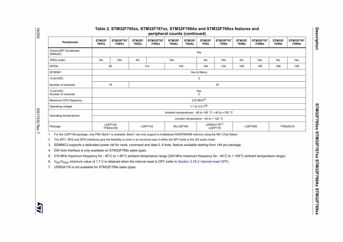
Chrom-ART Accelerator (DMA2D)
Yes
JPEG codec No Yes No Yes No Yes No Yes No Yes
GPIOs 82 114 129 140 132 168 159 168 159
DFSDM1 Yes (4 filters)
12-bit ADC
Number of channels
3
16 24
12-bit DAC Number of channels
Yes2
Maximum CPU frequency 216 MHz(5)
Operating voltage 1.7 to 3.6 V(6)
Operating temperaturesAmbient temperatures: –40 to +85 °C /–40 to +105 °C
Junction temperature: –40 to + 125 °C
PackageLQFP100
TFBGA100LQFP144 WLCSP180
UFBGA176(7) LQFP176
LQFP208 TFBGA216
1. For the LQFP100 package, only FMC Bank1 is available. Bank1 can only support a multiplexed NOR/PSRAM memory using the NE1 Chip Select.
2. The SPI1, SPI2 and SPI3 interfaces give the flexibility to work in an exclusive way in either the SPI mode or the I2S audio mode.
3. SDMMC2 supports a dedicated power rail for clock, command and data 0..4 lines, feature available starting from 144 pin package.
4. DSI host interface is only available on STM32F769x sales types.
5. 216 MHz maximum frequency for - 40°C to + 85°C ambient temperature range (200 MHz maximum frequency for - 40°C to + 105°C ambient temperature range).
6. VDD/VDDA minimum value of 1.7 V is obtained when the internal reset is OFF (refer to Section 3.18.2: Internal reset OFF).
7. UFBGA176 is not available for STM32F769x sales types.
Table 2. STM32F765xx, STM32F767xx, STM32F768Ax and STM32F769xx features andperipheral counts (continued)
PeripheralsSTM32F765Vx
STM32F767/769Vx
STM32F765Zx
STM32F767/769Zx
STM32F769Ax
STM32F768Ax
STM32F765Ix
STM32F767/769Ix
STM32F765Bx
STM32F767/769Bx
STM32F765Nx
STM32F767/769Nx
DS11532 Rev 7 19/252
STM32F765xx STM32F767xx STM32F768Ax STM32F769xx Description
54
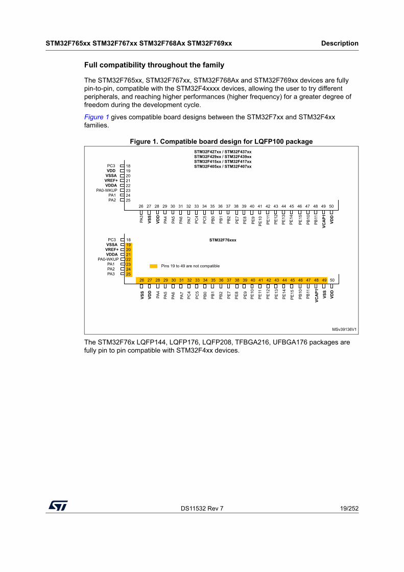
Full compatibility throughout the family
The STM32F765xx, STM32F767xx, STM32F768Ax and STM32F769xx devices are fully pin-to-pin, compatible with the STM32F4xxxx devices, allowing the user to try different peripherals, and reaching higher performances (higher frequency) for a greater degree of freedom during the development cycle.
Figure 1 gives compatible board designs between the STM32F7xx and STM32F4xx families.
Figure 1. Compatible board design for LQFP100 package
The STM32F76x LQFP144, LQFP176, LQFP208, TFBGA216, UFBGA176 packages are fully pin to pin compatible with STM32F4xx devices.
MSv39136V1
1819202122232425
PC3VDD
VSSAVREF+VDDA
26 27 28 29 30 31 32 33 34 35 36 37 38 39 40 41 42 43 44 45 46 47 48 49 50
PA3
VSS
VDD
PA4
PA5
PA6
PA7
PC
5
PB
0
PB
1
PB
2
PE
7
PE
8
PE
9
PE
10
PE
11
PE
12
PE
13
PE
14
PC
4
PB
10
PB
11
VCA
P1
VDD
PE
15
STM32F427xx / STM32F437xxSTM32F429xx / STM32F439xx STM32F415xx / STM32F417xx STM32F405xx / STM32F407xx
STM32F76xxx1819202122232425
26 27 28 29 30 31 32 33 34 35 36 37 38 39 40 41 42 43 44 45 46 47 48 49 50
VSS
VDD
VSS
PA4
PA5
PA6
PA7
PC
5
PB
0
PB
1
PB
2
PE
7
PE
8
PE
9
PE
10
PE
11
PE
12
PE
13
PE
14
PC
4
PB
10
PB
11
VCA
P1
VDD
PE
15
PC3VSSAVREF+VDDA
Pins 19 to 49 are not compatible
PA0-WKUP
PA1PA2PA3
PA0-WKUP
PA1PA2
Description STM32F765xx STM32F767xx STM32F768Ax STM32F769xx
20/252 DS11532 Rev 7
Figure 2. STM32F765xx, STM32F767xx, STM32F768Ax and STM32F769xx block diagram
1. The timers connected to APB2 are clocked from TIMxCLK up to 216 MHz, while the timers connected to APB1 are clocked from TIMxCLK either up to 108 MHz or 216 MHz depending on TIMPRE bit configuration in the RCC_DCKCFGR register.
MSv41056V2
GPIO PORT A
AHB/APB2
EXT IT. WKUP168 AF
PA[15:0]
TIM1 / PWM4 compl. chan. (TIM1_CH1[1:4]N),
4 chan. (TIM1_CH1[1:4]ETR, BKIN as AF
USART1RX, TX, SCK,CTS, RTS as AF
SPI1/I2S1
AP
B1
30
MH
z
8 analog inputs commonto the 3 ADCs
VDDREF_ADC
UART4
MOSI, MISO, SCKNSS as AF
SPI3/I2S3
TX, RXbxCAN2
DAC1as AF
ITF
WWDG
4 KB BKPRAM
OSC32_INOSC32_OUT
VDDA, VSSANRESET
smcardirDA
16b
SDMMC1D[7:0]CMD, CK as AF
VBAT = 1.8 to 3.6 V
GPDMA2
SCL, SDA, SMBAL as AFI2C3/SMBUS
Ethernet MAC10/100
DMA/FIFO
MII or RMII as AFMDIO as AF
USBOTG HS
DP, DMULPI:CK, D[7:0], DIR, STP, NXT
SCL/SDA, INT, ID, VBUSGP-DMA2
8 StreamsFIFO
ACCEL/CACHE
SRAM1 368KB
CLK, NE [3:0], A[23:0],D[31:0], NOEN, NWEN,NBL[3:0], SDCLKE[1:0], SDNE[1:0], SDNWE, NL
NWAIT, INTN
CameraITF
HSYNC, VSYNCPUIXCLK, D[13:0]
PH
YUSB
OTG FS
DPDMSCL, SDA, INT, ID, VBUSFI
FO
AHB1 216 MHz
PH
Y
FIFO
U S AR T 2 M B p sTemperature sensor
ADC1
ADC2
ADC3I FIF
POR/PDRBOR
SUPPLY SUPERVISION
PVD
Int
POR reset
XTAL 32 kHz
M G T
RTC
RC HS
RC LS
Standbyinterface
@VDDA
AWU
RCCReset & control
PLL1+PLL2+PLL3
AH
B1P
CLK
VDDUSB33 = 3.0 to 3.6 V
VSSVCAP1
VOLT. REG3.3V TO 1.2V
VDD12 BBgen + POWER MNGT
Backup register
AH
B b
us-m
atrix
8S
7M
AP
B2
108
MH
z (m
ax)
LS
TIM14TIM92 channels as AF
DAC1
FLASH 1MB
TIM6
TIM7
TIM2
TIM3
TIM4
TIM5
TIM12
AP
B1
54
MH
z (m
ax)
SRAM2 16 KB
AHB2 216 MHZDMA/FIFO
GP-DMA1
8 StreamsFIFO
PB[15:0]
PC[15:0]
PD[15:0]
PE[15:0]
PF[15:0]
PG[15:0]
PH[15:0]
PI[15:0]
GPIO PORT B
GPIO PORT C
GPIO PORT D
GPIO PORT E
GPIO PORT F
GPIO PORT G
GPIO PORT H
GPIO PORT I
TIM8 / PWM 16b
16b
TIM10 16b
TIM11 16b
smcardirDA
USART6
4 compl. chan.(TIM8_CH1[1:4]N),4 chan. (TIM8_CH1[1:4], ETR, BKIN as AF
1 channel as AF
1 channel as AF
RX, TX, SCK,CTS, RTS as AF
8 analog inputs commonto the ADC1 & 2
8 analog inputs for ADC3
DAC2as AF
16b
16b
bxCAN1
I2C2/SMBUS
I2C1/SMBUS
SCL, SDA, SMBAL as AF
SCL, SDA, SMBAL as AF
SPI2/I2S2MOSI, MISO, SCKNSS as AF
TX, RX
RX, TX as AF
RX, TX as AF
RX, TX, SCKCTS, RTS as AF
RX, TX, SCKCTS, RTS as AF
1 channel as AF
UART5
USART3
USART2
smcardirDA
smcardirDA
16b
16b
16b
1 channel as AFTIM13
2 channels as AF
32b
16b
16b
32b
4 channels
4 channels, ETR as AF
4 channels, ETR as AF
4 channels, ETR as AF
GPDMA1
AHB/APB1
LS
OSC_INOSC_OUT
AH
B2P
CLK
XTAL OSC4- 16MHz
FIFO
SPI4SCK, NSS as AFSPI5
SCK, NSS as AF
MOSI, MISO,
MOSI, MISO,SPI6
SCK, NSS as AFMOSI, MISO,
RX, TX as AFUART7
RX, TX as AFUART8
FIFOLCD-TFT
FIFOCHROM-ART
(DMA2D)
PJ[15:0] GPIO PORT J
PK[7:0] GPIO PORT K
SAI1SD, SCK, FS, MCLK as AF FIFO
NRAS, NCAS, NADV
LCD_R[7:0], LCD_G[7:0], LCD_B[7:0],LCD_HSYNC, LCD_VSYNC, LCD_DE,
LCD_CLK
RTC_TSRTC_TAMPxRTC_OUT
Arm CPUCortex-M7
AXIM
AHBPAHBS
DTCMICTMTRACECK
TRACED[3:0]
JTRST, JTDI,JTCK/SWCLK
JTDO/SWD, JTDO
JTAG & SWNVICETM
MPU FPU
DTCM RAM 128KB
ITCM RAM 16KB
Quad-SPICLK, CS,D[7:0]
AH
B B
US
-MAT
RIX
11S
8MVDDMMC33 = 1.8 to 3.6VWKUP[4:0]
LPTIM1 16b
HDMI_CEC as AFHDMI-CEC
SPDIFRX SPDIFRX[3:0] as AF
SCL, SDA, SMBAL as AFI2C4/SMBUS
SAI2SD, SCK, FS, MCLK as AF FIFO
EXT MEM CTL (FMC)SRAM, SDRAM, NOR-Flash, NAND-Flash, SDRAM
216MHz
I-Cache 16KBD-Cache 16KB
AH
B2A
XI
@VDDA
@VDD33
@VDD33
@VSW
Dig
ital f
ilter
@VDDA
@VDDA
FLASH 1MB
FIFO JPEG
SDMMC2D[7:0]CMD, CK as AF
DFSDM
MDIO Slave
CKIN[7:0]DATAIN[7:0]
CKOUTCKIN[7:0]
DATAIN[7:0]CKOUT
DAC2
DSI_DOP/N, DSI_D1P/NDSI_VCAP, DSI_CKP/NDSI_VDD12, DSI_VSS, DSI_TE as AF
PLL
@V
DD
A
DSI PHY
LDO
SYSCFG
DSI HOST
bxCAN3
FIFO
TX, RX
WDG32K
VDD = 1.8 to 3.6 V
PW
RC
TRL
FCLK
HC
LKA
PB
P2C
LKA
PB
P1C
LK
CRC
SCK, NSS as AFMOSI, MISO,
FIFO
RNG
DS11532 Rev 7 21/252
STM32F765xx STM32F767xx STM32F768Ax STM32F769xx Functional overview
54
3 Functional overview
3.1 Arm® Cortex®-M7 with FPU
The Arm® Cortex®-M7 with FPU processor is the latest generation of Arm processors for embedded systems. It was developed to provide a low-cost platform that meets the needs of MCU implementation, with a reduced pin count and low-power consumption, while delivering an outstanding computational performance and low interrupt latency.
The Cortex®-M7 processor is a highly efficient high-performance featuring:
– Six-stage dual-issue pipeline
– Dynamic branch prediction
– Harvard caches (16 Kbytes of I-cache and 16 Kbytes of D-cache)
– 64-bit AXI4 interface
– 64-bit ITCM interface
– 2x32-bit DTCM interfaces
The processor supports the following memory interfaces:
• Tightly Coupled Memory (TCM) interface.
• Harvard instruction and data caches and AXI master (AXIM) interface.
• Dedicated low-latency AHB-Lite peripheral (AHBP) interface.
The processor supports a set of DSP instructions which allow an efficient signal processing and a complex algorithm execution.
It supports single and double precision FPU (floating point unit), speeds up software development by using metalanguage development tools, while avoiding saturation.
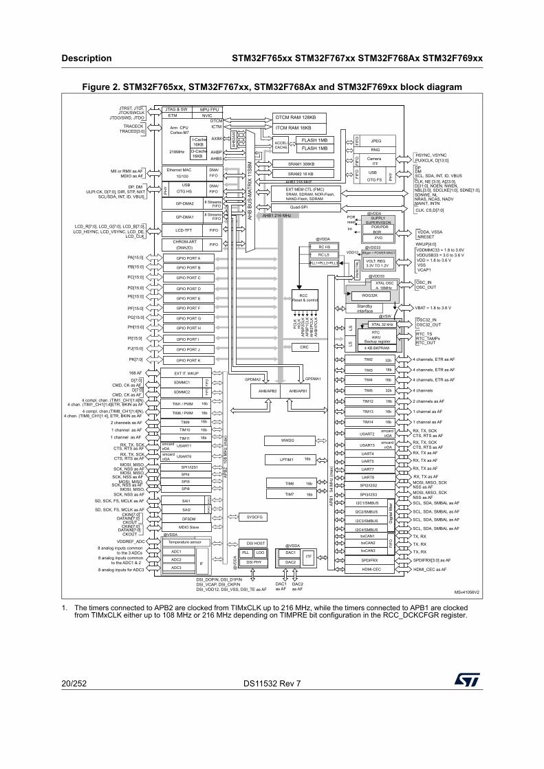
Figure 2 shows the general block diagram of the STM32F76xxx family.
Note: The Cortex®-M7 with FPU core is binary compatible with the Cortex®-M4 core.
3.2 Memory protection unit
The memory protection unit (MPU) is used to manage the CPU accesses to memory to prevent one task to accidentally corrupt the memory or resources used by any other active task. This memory area is organized into up to 8 protected areas that can in turn be divided up into 8 subareas. The protection area sizes are between 32 bytes and the whole 4 gigabytes of addressable memory.
The MPU is especially helpful for applications where some critical or certified code has to be protected against the misbehavior of other tasks. It is usually managed by an RTOS (real-time operating system). If a program accesses a memory location that is prohibited by the MPU, the RTOS can detect it and take action. In an RTOS environment, the kernel can dynamically update the MPU area setting, based on the process to be executed.
The MPU is optional and can be bypassed for applications that do not need it.
Functional overview STM32F765xx STM32F767xx STM32F768Ax STM32F769xx
22/252 DS11532 Rev 7
3.3 Embedded Flash memory
The STM32F765xx, STM32F767xx, STM32F768Ax and STM32F769xx devices embed a Flash memory of up to 2 Mbytes available for storing programs and data. The Flash interface features:
• Single /or Dual bank operating modes,
• Read-While-Write (RWW) in Dual bank mode.
3.4 CRC (cyclic redundancy check) calculation unit
The CRC (cyclic redundancy check) calculation unit is used to get a CRC code using a configurable generator polynomial value and size.
Among other applications, CRC-based techniques are used to verify data transmission or storage integrity. In the scope of the EN/IEC 60335-1 standard, they offer a means of verifying the Flash memory integrity. The CRC calculation unit helps compute a signature of the software during runtime, to be compared with a reference signature generated at link-time and stored at a given memory location.
3.5 Embedded SRAM
All the devices feature:
• System SRAM up to 512 Kbytes:
– SRAM1 on AHB bus Matrix: 368 Kbytes
– SRAM2 on AHB bus Matrix: 16 Kbytes
– DTCM-RAM on TCM interface (Tighly Coupled Memory interface): 128 Kbytes for critical real-time data.
• Instruction RAM (ITCM-RAM) 16 Kbytes:
– It is mapped on TCM interface and reserved only for CPU Execution/Instruction useful for critical real-time routines.
The Data TCM RAM is accessible by the GP-DMAs and peripherals DMAs through specific AHB slave of the CPU.The instruction TCM RAM is reserved only for CPU. It is accessed at CPU clock speed with 0 wait states.
• 4 Kbytes of backup SRAM
This area is accessible only from the CPU. Its content is protected against possible unwanted write accesses, and is retained in Standby or VBAT mode.
DS11532 Rev 7 23/252
STM32F765xx STM32F767xx STM32F768Ax STM32F769xx Functional overview
54
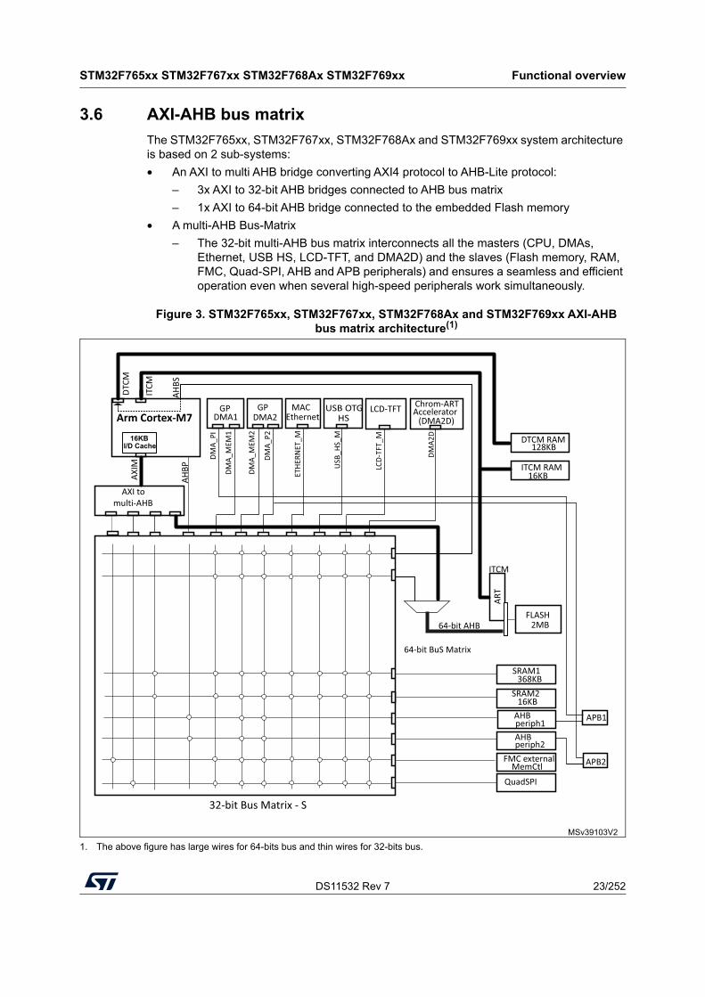
3.6 AXI-AHB bus matrix
The STM32F765xx, STM32F767xx, STM32F768Ax and STM32F769xx system architecture is based on 2 sub-systems:
• An AXI to multi AHB bridge converting AXI4 protocol to AHB-Lite protocol:
– 3x AXI to 32-bit AHB bridges connected to AHB bus matrix
– 1x AXI to 64-bit AHB bridge connected to the embedded Flash memory
• A multi-AHB Bus-Matrix
– The 32-bit multi-AHB bus matrix interconnects all the masters (CPU, DMAs, Ethernet, USB HS, LCD-TFT, and DMA2D) and the slaves (Flash memory, RAM, FMC, Quad-SPI, AHB and APB peripherals) and ensures a seamless and efficient operation even when several high-speed peripherals work simultaneously.
Figure 3. STM32F765xx, STM32F767xx, STM32F768Ax and STM32F769xx AXI-AHBbus matrix architecture(1)
1. The above figure has large wires for 64-bits bus and thin wires for 32-bits bus.
MSv39103V2
Arm Cortex-M7
32-bit Bus Matrix - S
ART
FLASH2MB
SRAM1 368KB
SRAM216KB
AHBperiph2
FMC externalMemCtl
QuadSPI
AHBP
AXI to multi-AHB
AHBperiph1
DTCM RAM
ITCM RAM
DTCM
ITCM
AXIM
16KB
128KB
64-bit AHB
64-bit BuS Matrix
ITCM
APB1
APB2
AHBS
I/D Cache16KB
GPDMA1
GPDMA2
MACEthernet
USB OTGHS
DMA_
PI
DMA_
MEM
1
DMA_
MEM
2
DMA_
P2
ETHE
RNET
_M
USB
_HS_
M
LCD-TFT Chrom-ART
LCD-
TFT_
M
DMA2
D
Accelerator (DMA2D)
Functional overview STM32F765xx STM32F767xx STM32F768Ax STM32F769xx
24/252 DS11532 Rev 7
3.7 DMA controller (DMA)
The devices feature two general-purpose dual-port DMAs (DMA1 and DMA2) with 8 streams each. They are able to manage memory-to-memory, peripheral-to-memory and memory-to-peripheral transfers. They feature dedicated FIFOs for APB/AHB peripherals, support burst transfer and are designed to provide the maximum peripheral bandwidth (AHB/APB).
The two DMA controllers support circular buffer management, so that no specific code is needed when the controller reaches the end of the buffer. The two DMA controllers also have a double buffering feature, which automates the use and switching of two memory buffers without requiring any special code.
Each stream is connected to dedicated hardware DMA requests, with support for software trigger on each stream. The configuration is made by software and the transfer sizes between the source and the destination are independent.
The DMA can be used with the main peripherals:
• SPI and I2S
• I2C
• USART
• General-purpose, basic and advanced-control timers TIMx
• DAC
• SDMMC
• Camera interface (DCMI)
• ADC
• SAI
• SPDIFRX
• Quad-SPI
• HDMI-CEC
• JPEG codec
• DFSDM1
DS11532 Rev 7 25/252
STM32F765xx STM32F767xx STM32F768Ax STM32F769xx Functional overview
54
3.8 Flexible memory controller (FMC)
The Flexible memory controller (FMC) includes three memory controllers:• The NOR/PSRAM memory controller
• The NAND/memory controller
• The Synchronous DRAM (SDRAM/Mobile LPSDR SDRAM) controller
The main features of the FMC controller are the following:• Interface with static-memory mapped devices including:
– Static random access memory (SRAM)
– NOR Flash memory/OneNAND Flash memory
– PSRAM (4 memory banks)
– NAND Flash memory with ECC hardware to check up to 8 Kbytes of data
• Interface with synchronous DRAM (SDRAM/Mobile LPSDR SDRAM) memories
• 8-,16-,32-bit data bus width
• Independent Chip Select control for each memory bank
• Independent configuration for each memory bank
• Write FIFO
• Read FIFO for SDRAM controller
• The maximum FMC_CLK/FMC_SDCLK frequency for synchronous accesses is HCLK/2
LCD parallel interface
The FMC can be configured to interface seamlessly with most graphic LCD controllers. It supports the Intel 8080 and Motorola 6800 modes, and is flexible enough to adapt to specific LCD interfaces. This LCD parallel interface capability makes it easy to build cost-effective graphic applications using LCD modules with embedded controllers or high performance solutions using external controllers with dedicated acceleration.
3.9 Quad-SPI memory interface (QUADSPI)
All the devices embed a Quad-SPI memory interface, which is a specialized communication interface targetting Single, Dual or Quad-SPI Flash memories. It can work in:
• Direct mode through registers
• External Flash status register polling mode
• Memory mapped mode.
Up to 256 Mbytes external Flash are memory mapped, supporting 8, 16 and 32-bit access. Code execution is supported.
The opcode and the frame format are fully programmable. The communication can be either in Single Data Rate or Dual Data Rate.
Functional overview STM32F765xx STM32F767xx STM32F768Ax STM32F769xx
26/252 DS11532 Rev 7
3.10 LCD-TFT controller
The LCD-TFT display controller provides a 24-bit parallel digital RGB (Red, Green, Blue) and delivers all signals to interface directly to a broad range of LCD and TFT panels up to XGA (1024x768) resolution with the following features:
• 2 display layers with dedicated FIFO (64x32-bit)
• Color Look-Up table (CLUT) up to 256 colors (256x24-bit) per layer
• Up to 8 input color formats selectable per layer
• Flexible blending between two layers using alpha value (per pixel or constant)
• Flexible programmable parameters for each layer
• Color keying (transparency color)
• Up to 4 programmable interrupt events
3.11 Chrom-ART Accelerator (DMA2D)
The Chrom-Art Accelerator (DMA2D) is a graphic accelerator which offers advanced bit blitting, row data copy and pixel format conversion. It supports the following functions:
• Rectangle filling with a fixed color
• Rectangle copy
• Rectangle copy with pixel format conversion
• Rectangle composition with blending and pixel format conversion
Various image format codings are supported, from indirect 4bpp color mode up to 32bpp direct color. It embeds dedicated memory to store color lookup tables.
An interrupt can be generated when an operation is complete or at a programmed watermark.
All the operations are fully automatized and are running independently from the CPU or the DMAs.
3.12 Nested vectored interrupt controller (NVIC)
The devices embed a nested vectored interrupt controller able to manage 16 priority levels, and handle up to 110 maskable interrupt channels plus the 16 interrupt lines of the Cortex®-M7 with FPU core.
• Closely coupled NVIC gives low-latency interrupt processing
• Interrupt entry vector table address passed directly to the core
• Allows early processing of interrupts
• Processing of late arriving, higher-priority interrupts
• Support tail chaining
• Processor state automatically saved
• Interrupt entry restored on interrupt exit with no instruction overhead
This hardware block provides flexible interrupt management features with minimum interrupt latency.
DS11532 Rev 7 27/252
STM32F765xx STM32F767xx STM32F768Ax STM32F769xx Functional overview
54
3.13 JPEG codec (JPEG)
The JPEG codec provides an fast and simple hardware compressor and decompressor of JPEG images with full management of JPEG headers.
The JPEG codec main features:
• 8-bit/channel pixel depths
• Single clock per pixel encoding and decoding
• Support for JPEG header generation and parsing
• Up to four programmable quantization tables
• Fully programmable Huffman tables (two AC and two DC)
• Fully programmable minimum coded unit (MCU)
• Encode/decode support (non simultaneous)
• Single clock Huffman coding and decoding
• Two-channel interface: Pixel/Compress In, Pixel/Compressed Out
• Stallable design
• Support for single, greyscale component
• Functionality to enable/disable header processing
• Internal register interface
• Fully synchronous design
• Configured for high-speed decode mode
3.14 External interrupt/event controller (EXTI)
The external interrupt/event controller consists of 25 edge-detector lines used to generate interrupt/event requests. Each line can be independently configured to select the trigger event (rising edge, falling edge, both) and can be masked independently. A pending register maintains the status of the interrupt requests. The EXTI can detect an external line with a pulse width shorter than the Internal APB2 clock period. Up to 168 GPIOs can be connected to the 16 external interrupt lines.
3.15 Clocks and startup
On reset the 16 MHz internal HSI RC oscillator is selected as the default CPU clock. The 16 MHz internal RC oscillator is factory-trimmed to offer 1% accuracy. The application can then select as system clock either the RC oscillator or an external 4-26 MHz clock source. This clock can be monitored for failure. If a failure is detected, the system automatically switches back to the internal RC oscillator and a software interrupt is generated (if enabled). This clock source is input to a PLL thus allowing to increase the frequency up to 216 MHz. Similarly, full interrupt management of the PLL clock entry is available when necessary (for example if an indirectly used external oscillator fails).
Several prescalers allow the configuration of the two AHB buses, the high-speed APB (APB2) and the low-speed APB (APB1) domains. The maximum frequency of the two AHB buses is 216 MHz while the maximum frequency of the high-speed APB domains is 108 MHz. The maximum allowed frequency of the low-speed APB domain is 54 MHz.
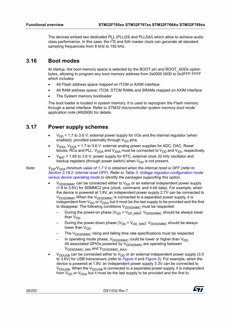
Functional overview STM32F765xx STM32F767xx STM32F768Ax STM32F769xx
28/252 DS11532 Rev 7
The devices embed two dedicated PLL (PLLI2S and PLLSAI) which allow to achieve audio class performance. In this case, the I2S and SAI master clock can generate all standard sampling frequencies from 8 kHz to 192 kHz.
3.16 Boot modes
At startup, the boot memory space is selected by the BOOT pin and BOOT_ADDx option bytes, allowing to program any boot memory address from 0x0000 0000 to 0x3FFF FFFF which includes:
• All Flash address space mapped on ITCM or AXIM interface
• All RAM address space: ITCM, DTCM RAMs and SRAMs mapped on AXIM interface
• The System memory bootloader
The boot loader is located in system memory. It is used to reprogram the Flash memory through a serial interface. Refer to STM32 microcontroller system memory boot mode application note (AN2606) for details.
3.17 Power supply schemes
• VDD = 1.7 to 3.6 V: external power supply for I/Os and the internal regulator (when enabled), provided externally through VDD pins.
• VSSA, VDDA = 1.7 to 3.6 V: external analog power supplies for ADC, DAC, Reset blocks, RCs and PLL. VDDA and VSSA must be connected to VDD and VSS, respectively.
• VBAT = 1.65 to 3.6 V: power supply for RTC, external clock 32 kHz oscillator and backup registers (through power switch) when VDD is not present.
Note: VDD/VDDA minimum value of 1.7 V is obtained when the internal reset is OFF (refer to Section 3.18.2: Internal reset OFF). Refer to Table 3: Voltage regulator configuration mode versus device operating mode to identify the packages supporting this option.
• VDDSDMMC can be connected either to VDD or an external independent power supply (1.8 to 3.6V) for SDMMC2 pins (clock, command, and 4-bit data). For example, when the device is powered at 1.8V, an independent power supply 2.7V can be connected to VDDSDMMC.When the VDDSDMMC is connected to a separated power supply, it is independent from VDD or VDDA but it must be the last supply to be provided and the first to disappear. The following conditions VDDSDMMC must be respected:
– During the power-on phase (VDD < VDD_MIN), VDDSDMMC should be always lower than VDD
– During the power-down phase (VDD < VDD_MIN), VDDSDMMC should be always lower than VDD
– The VDDSDMMC rising and falling time rate specifications must be respected
– In operating mode phase, VDDSDMMC could be lower or higher than VDD: All associated GPIOs powered by VDDSDMMC are operating between VDDSDMMC_MIN and VDDSDMMC_MAX.
• VDDUSB can be connected either to VDD or an external independent power supply (3.0 to 3.6V) for USB transceivers (refer to Figure 4 and Figure 5). For example, when the device is powered at 1.8V, an independent power supply 3.3V can be connected to VDDUSB. When the VDDUSB is connected to a separated power supply, it is independent from VDD or VDDA but it must be the last supply to be provided and the first to
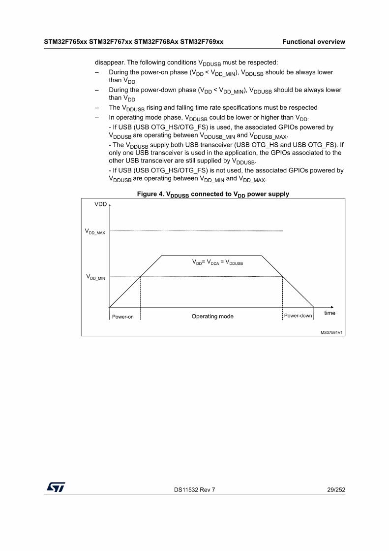
DS11532 Rev 7 29/252
STM32F765xx STM32F767xx STM32F768Ax STM32F769xx Functional overview
54
disappear. The following conditions VDDUSB must be respected:
– During the power-on phase (VDD < VDD_MIN), VDDUSB should be always lower than VDD
– During the power-down phase (VDD < VDD_MIN), VDDUSB should be always lower than VDD
– The VDDUSB rising and falling time rate specifications must be respected
– In operating mode phase, VDDUSB could be lower or higher than VDD:
- If USB (USB OTG_HS/OTG_FS) is used, the associated GPIOs powered by VDDUSB are operating between VDDUSB_MIN and VDDUSB_MAX.
- The VDDUSB supply both USB transceiver (USB OTG_HS and USB OTG_FS). If only one USB transceiver is used in the application, the GPIOs associated to the other USB transceiver are still supplied by VDDUSB.
- If USB (USB OTG_HS/OTG_FS) is not used, the associated GPIOs powered by VDDUSB are operating between VDD_MIN and VDD_MAX.
Figure 4. VDDUSB connected to VDD power supply
VDD_MIN
time
VDD= VDDA = VDDUSB
Power-on Power-downOperating mode
VDD_MAX
VDD
MS37591V1
Functional overview STM32F765xx STM32F767xx STM32F768Ax STM32F769xx
30/252 DS11532 Rev 7
Figure 5. VDDUSB connected to external power supply
The DSI (Display Serial Interface) sub-system uses several power supply pins which are
independent from the other supply pins:
• VDDDSI is an independent DSI power supply dedicated for DSI Regulator and MIPI D-PHY. This supply must be connected to global VDD.
• The VCAPDSI pin is the output of DSI Regulator (1.2V) which must be connected externally to VDD12DSI.
• The VDD12DSI pin is used to supply the MIPI D-PHY, and to supply the clock and data lanes pins. An external capacitor of 2.2 uF must be connected on the VDD12DSI pin.
• The VSSDSI pin is an isolated supply ground used for DSI sub-system.
• If the DSI functionality is not used at all, then:
– The VDDDSI pin must be connected to global VDD.
– The VCAPDSI pin must be connected externally to VDD12DSI but the external capacitor is no more needed.
– The VSSDSI pin must be grounded.
3.18 Power supply supervisor
3.18.1 Internal reset ON
On packages embedding the PDR_ON pin, the power supply supervisor is enabled by holding PDR_ON high. On the other packages, the power supply supervisor is always enabled.
The device has an integrated power-on reset (POR)/ power-down reset (PDR) circuitry coupled with a Brownout reset (BOR) circuitry. At power-on, POR/PDR is always active and ensures proper operation starting from 1.8 V. After the 1.8 V POR threshold level is reached, the option byte loading process starts, either to confirm or modify default BOR thresholds, or to disable BOR permanently. Three BOR thresholds are available through
MS37590V1
VDDUSB_MIN
VDD_MIN
time
VDDUSB_MAXUSB functional area
VDD = VDDA
USB nonfunctionalarea
VDDUSB
Power-on Power-downOperating mode
USB nonfunctionalarea
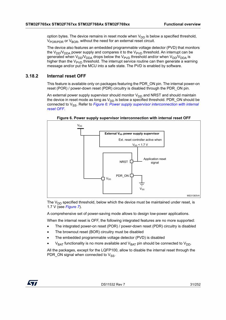
DS11532 Rev 7 31/252
STM32F765xx STM32F767xx STM32F768Ax STM32F769xx Functional overview
54
option bytes. The device remains in reset mode when VDD is below a specified threshold, VPOR/PDR or VBOR, without the need for an external reset circuit.
The device also features an embedded programmable voltage detector (PVD) that monitors the VDD/VDDA power supply and compares it to the VPVD threshold. An interrupt can be generated when VDD/VDDA drops below the VPVD threshold and/or when VDD/VDDA is higher than the VPVD threshold. The interrupt service routine can then generate a warning message and/or put the MCU into a safe state. The PVD is enabled by software.
3.18.2 Internal reset OFF
This feature is available only on packages featuring the PDR_ON pin. The internal power-on reset (POR) / power-down reset (PDR) circuitry is disabled through the PDR_ON pin.
An external power supply supervisor should monitor VDD and NRST and should maintain the device in reset mode as long as VDD is below a specified threshold. PDR_ON should be connected to VSS. Refer to Figure 6: Power supply supervisor interconnection with internal reset OFF.
Figure 6. Power supply supervisor interconnection with internal reset OFF
The VDD specified threshold, below which the device must be maintained under reset, is 1.7 V (see Figure 7).
A comprehensive set of power-saving mode allows to design low-power applications.
When the internal reset is OFF, the following integrated features are no more supported:
• The integrated power-on reset (POR) / power-down reset (PDR) circuitry is disabled
• The brownout reset (BOR) circuitry must be disabled
• The embedded programmable voltage detector (PVD) is disabled
• VBAT functionality is no more available and VBAT pin should be connected to VDD.
All the packages, except for the LQFP100, allow to disable the internal reset through the PDR_ON signal when connected to VSS.
MS31383V4
NRST
VDD
PDR_ON
External VDD power supply supervisor
Ext. reset controller active whenVDD < 1.7 V
VDD
Application resetsignal
VSS
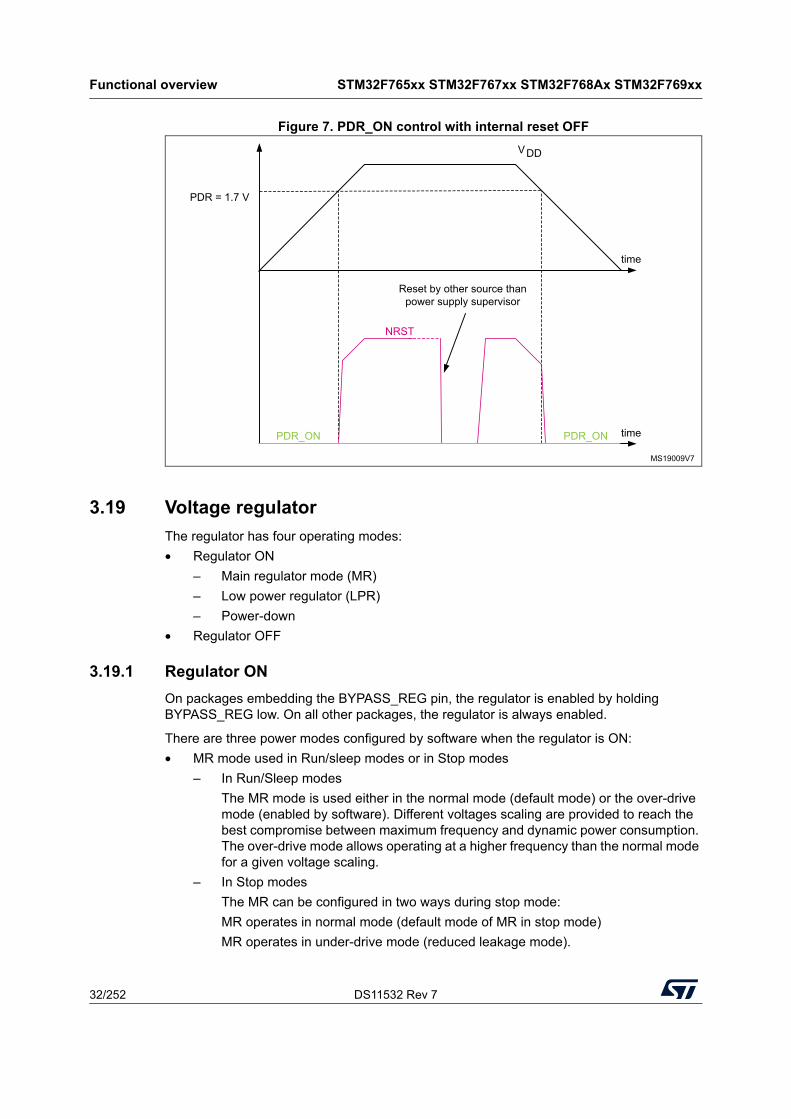
Functional overview STM32F765xx STM32F767xx STM32F768Ax STM32F769xx
32/252 DS11532 Rev 7
Figure 7. PDR_ON control with internal reset OFF
3.19 Voltage regulator
The regulator has four operating modes:
• Regulator ON
– Main regulator mode (MR)
– Low power regulator (LPR)
– Power-down
• Regulator OFF
3.19.1 Regulator ON
On packages embedding the BYPASS_REG pin, the regulator is enabled by holding BYPASS_REG low. On all other packages, the regulator is always enabled.
There are three power modes configured by software when the regulator is ON:
• MR mode used in Run/sleep modes or in Stop modes
– In Run/Sleep modes
The MR mode is used either in the normal mode (default mode) or the over-drive mode (enabled by software). Different voltages scaling are provided to reach the best compromise between maximum frequency and dynamic power consumption. The over-drive mode allows operating at a higher frequency than the normal mode for a given voltage scaling.
– In Stop modes
The MR can be configured in two ways during stop mode:
MR operates in normal mode (default mode of MR in stop mode)
MR operates in under-drive mode (reduced leakage mode).
MS19009V7
VDD
time
PDR = 1.7 V
time
NRST
PDR_ON PDR_ON
Reset by other source than power supply supervisor
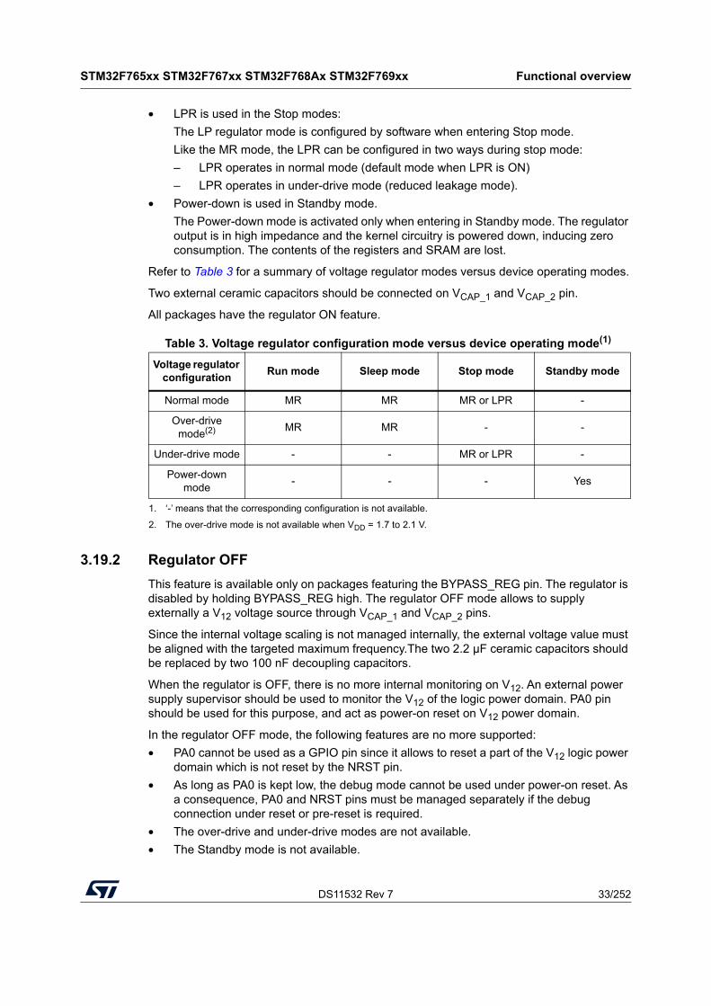
DS11532 Rev 7 33/252
STM32F765xx STM32F767xx STM32F768Ax STM32F769xx Functional overview
54
• LPR is used in the Stop modes:
The LP regulator mode is configured by software when entering Stop mode.
Like the MR mode, the LPR can be configured in two ways during stop mode:
– LPR operates in normal mode (default mode when LPR is ON)
– LPR operates in under-drive mode (reduced leakage mode).
• Power-down is used in Standby mode.
The Power-down mode is activated only when entering in Standby mode. The regulator output is in high impedance and the kernel circuitry is powered down, inducing zero consumption. The contents of the registers and SRAM are lost.
Refer to Table 3 for a summary of voltage regulator modes versus device operating modes.
Two external ceramic capacitors should be connected on VCAP_1 and VCAP_2 pin.
All packages have the regulator ON feature.
3.19.2 Regulator OFF
This feature is available only on packages featuring the BYPASS_REG pin. The regulator is disabled by holding BYPASS_REG high. The regulator OFF mode allows to supply externally a V12 voltage source through VCAP_1 and VCAP_2 pins.
Since the internal voltage scaling is not managed internally, the external voltage value must be aligned with the targeted maximum frequency.The two 2.2 µF ceramic capacitors should be replaced by two 100 nF decoupling capacitors.
When the regulator is OFF, there is no more internal monitoring on V12. An external power supply supervisor should be used to monitor the V12 of the logic power domain. PA0 pin should be used for this purpose, and act as power-on reset on V12 power domain.
In the regulator OFF mode, the following features are no more supported:
• PA0 cannot be used as a GPIO pin since it allows to reset a part of the V12 logic power domain which is not reset by the NRST pin.
• As long as PA0 is kept low, the debug mode cannot be used under power-on reset. As a consequence, PA0 and NRST pins must be managed separately if the debug connection under reset or pre-reset is required.
• The over-drive and under-drive modes are not available.
• The Standby mode is not available.
Table 3. Voltage regulator configuration mode versus device operating mode(1)
1. ‘-’ means that the corresponding configuration is not available.
Voltage regulator configuration
Run mode Sleep mode Stop mode Standby mode
Normal mode MR MR MR or LPR -
Over-drive mode(2)
2. The over-drive mode is not available when VDD = 1.7 to 2.1 V.
MR MR - -
Under-drive mode - - MR or LPR -
Power-down mode
- - - Yes
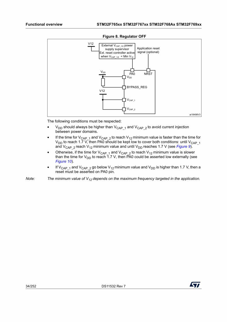
Functional overview STM32F765xx STM32F767xx STM32F768Ax STM32F769xx
34/252 DS11532 Rev 7
Figure 8. Regulator OFF
The following conditions must be respected:
• VDD should always be higher than VCAP_1 and VCAP_2 to avoid current injection between power domains.
• If the time for VCAP_1 and VCAP_2 to reach V12 minimum value is faster than the time for VDD to reach 1.7 V, then PA0 should be kept low to cover both conditions: until VCAP_1 and VCAP_2 reach V12 minimum value and until VDD reaches 1.7 V (see Figure 9).
• Otherwise, if the time for VCAP_1 and VCAP_2 to reach V12 minimum value is slower than the time for VDD to reach 1.7 V, then PA0 could be asserted low externally (see Figure 10).
• If VCAP_1 and VCAP_2 go below V12 minimum value and VDD is higher than 1.7 V, then a reset must be asserted on PA0 pin.
Note: The minimum value of V12 depends on the maximum frequency targeted in the application.
ai18498V3
BYPASS_REG
VCAP_1
VCAP_2
PA0
V12
VDD NRST VDD
Application reset signal (optional)
External VCAP_1/2 power supply supervisor
Ext. reset controller active when VCAP_1/2 < Min V12
V12
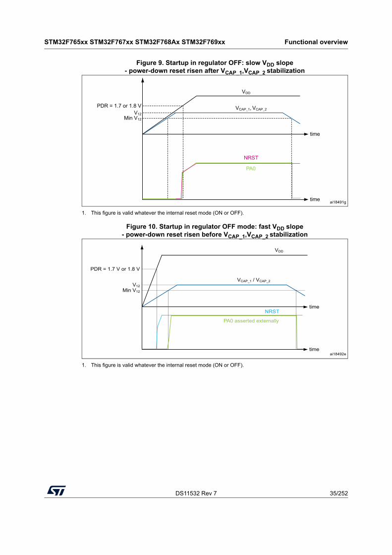
DS11532 Rev 7 35/252
STM32F765xx STM32F767xx STM32F768Ax STM32F769xx Functional overview
54
Figure 9. Startup in regulator OFF: slow VDD slope - power-down reset risen after VCAP_1,VCAP_2 stabilization
1. This figure is valid whatever the internal reset mode (ON or OFF).
Figure 10. Startup in regulator OFF mode: fast VDD slope - power-down reset risen before VCAP_1,VCAP_2 stabilization
1. This figure is valid whatever the internal reset mode (ON or OFF).
ai18491g
VDD
time
Min V12
PDR = 1.7 or 1.8 V VCAP_1, VCAP_2V12
NRST
time
PA0
VDD
time
Min V12
VCAP_1 / VCAP_2V12
PA0 asserted externally
NRST
timeai18492e
PDR = 1.7 V or 1.8 V
Functional overview STM32F765xx STM32F767xx STM32F768Ax STM32F769xx
36/252 DS11532 Rev 7
3.19.3 Regulator ON/OFF and internal reset ON/OFF availability
3.20 Real-time clock (RTC), backup SRAM and backup registers
The RTC is an independent BCD timer/counter. It supports the following features:
• Calendar with subsecond, seconds, minutes, hours (12 or 24 format), week day, date, month, year, in BCD (binary-coded decimal) format.
• Automatic correction for 28, 29 (leap year), 30, and 31 days of the month.
• Two programmable alarms.
• On-the-fly correction from 1 to 32767 RTC clock pulses. This can be used to synchronize it with a master clock.
• Reference clock detection: a more precise second source clock (50 or 60 Hz) can be used to enhance the calendar precision.
• Digital calibration circuit with 0.95 ppm resolution, to compensate for quartz crystal inaccuracy.
• Three anti-tamper detection pins with programmable filter.
• Timestamp feature which can be used to save the calendar content. This function can be triggered by an event on the timestamp pin, or by a tamper event, or by a switch to VBAT mode.
• 17-bit auto-reload wakeup timer (WUT) for periodic events with programmable resolution and period.
The RTC and the 32 backup registers are supplied through a switch that takes power either from the VDD supply when present or from the VBAT pin.
The backup registers are 32-bit registers used to store 128 bytes of user application data when VDD power is not present. They are not reset by a system or power reset, or when the device wakes up from Standby mode.
Table 4. Regulator ON/OFF and internal reset ON/OFF availability
Package Regulator ON Regulator OFF Internal reset ON Internal reset OFF
LQFP100
Yes No
Yes No
LQFP144, LQFP208
Yes
PDR_ON set to VDD
Yes
PDR_ON set to VSS
LQFP176,
UFBGA176,
TFBGA100,
TFBGA216
Yes
BYPASS_REG set to VSS
Yes
BYPASS_REG set to VDD
WLCSP180 Yes(1)
1. Available only on dedicated part number. Refer to Section 8: Ordering information.
DS11532 Rev 7 37/252
STM32F765xx STM32F767xx STM32F768Ax STM32F769xx Functional overview
54
The RTC clock sources can be:
• A 32.768 kHz external crystal (LSE)
• An external resonator or oscillator(LSE)
• The internal low power RC oscillator (LSI, with typical frequency of 32 kHz)
• The high-speed external clock (HSE) divided by 32
The RTC is functional in VBAT mode and in all low-power modes when it is clocked by the LSE. When clocked by the LSI, the RTC is not functional in VBAT mode, but is functional in all low-power modes.
All RTC events (Alarm, WakeUp Timer, Timestamp or Tamper) can generate an interrupt and wakeup the device from the low-power modes.
3.21 Low-power modes
The devices support three low-power modes to achieve the best compromise between low power consumption, short startup time and available wakeup sources:
• Sleep mode
In Sleep mode, only the CPU is stopped. All peripherals continue to operate and can wake up the CPU when an interrupt/event occurs.
• Stop mode
The Stop mode achieves the lowest power consumption while retaining the contents of SRAM and registers. All clocks in the 1.2 V domain are stopped, the PLL, the HSI RC and the HSE crystal oscillators are disabled.
The voltage regulator can be put either in main regulator mode (MR) or in low-power mode (LPR). Both modes can be configured as follows (see Table 5: Voltage regulator modes in stop mode):
– Normal mode (default mode when MR or LPR is enabled)
– Under-drive mode.
The device can be woken up from the Stop mode by any of the EXTI line (the EXTI line source can be one of the 16 external lines, the PVD output, the RTC alarm / wakeup / tamper / time stamp events, the USB OTG FS/HS wakeup or the Ethernet wakeup and LPTIM1 asynchronous interrupt).
• Standby mode
The Standby mode is used to achieve the lowest power consumption. The internal voltage regulator is switched off so that the entire 1.2 V domain is powered off. The PLL, the HSI RC and the HSE crystal oscillators are also switched off. After entering
Table 5. Voltage regulator modes in stop mode
Voltage regulator configuration
Main regulator (MR) Low-power regulator (LPR)
Normal mode MR ON LPR ON
Under-drive mode MR in under-drive mode LPR in under-drive mode
Functional overview STM32F765xx STM32F767xx STM32F768Ax STM32F769xx
38/252 DS11532 Rev 7
Standby mode, the SRAM and register contents are lost except for registers in the backup domain and the backup SRAM when selected.
The device exits the Standby mode when an external reset (NRST pin), an IWDG reset, a rising or falling edge on one of the 6 WKUP pins (PA0, PA2, PC1, PC13, PI8, PI11), or an RTC alarm / wakeup / tamper /time stamp event occurs.
The Standby mode is not supported when the embedded voltage regulator is bypassed and the 1.2 V domain is controlled by an external power.
3.22 VBAT operation
The VBAT pin allows to power the device VBAT domain from an external battery, an external supercapacitor, or from VDD when no external battery and an external supercapacitor are present.
VBAT operation is activated when VDD is not present.
The VBAT pin supplies the RTC, the backup registers and the backup SRAM.
Note: When the microcontroller is supplied from VBAT, external interrupts and RTC alarm/events do not exit it from VBAT operation.
When the PDR_ON pin is connected to VSS (Internal Reset OFF), the VBAT functionality is no more available and the VBAT pin should be connected to VDD.
3.23 Timers and watchdogs
The devices include two advanced-control timers, eight general-purpose timers, two basic timers and two watchdog timers.
All timer counters can be frozen in debug mode.
Table 6 compares the features of the advanced-control, general-purpose and basic timers.
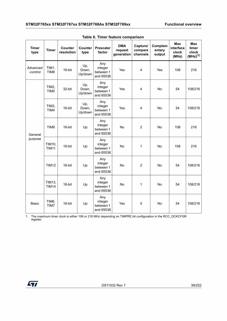
DS11532 Rev 7 39/252
STM32F765xx STM32F767xx STM32F768Ax STM32F769xx Functional overview
54
Table 6. Timer feature comparison
Timer type
TimerCounter
resolutionCounter
typePrescaler
factor
DMA request
generation
Capture/compare channels
Complementary output
Max interface
clock (MHz)
Max timer clock
(MHz)(1)
Advanced-control
TIM1, TIM8
16-bitUp,
Down, Up/down
Any integer
between 1 and 65536
Yes 4 Yes 108 216
General purpose
TIM2, TIM5
32-bitUp,
Down, Up/down
Any integer
between 1 and 65536
Yes 4 No 54 108/216
TIM3, TIM4
16-bitUp,
Down, Up/down
Any integer
between 1 and 65536
Yes 4 No 54 108/216
TIM9 16-bit Up
Any integer
between 1 and 65536
No 2 No 108 216
TIM10, TIM11
16-bit Up
Any integer
between 1 and 65536
No 1 No 108 216
TIM12 16-bit Up
Any integer
between 1 and 65536
No 2 No 54 108/216
TIM13, TIM14
16-bit Up
Any integer
between 1 and 65536
No 1 No 54 108/216
BasicTIM6, TIM7
16-bit Up
Any integer
between 1 and 65536
Yes 0 No 54 108/216
1. The maximum timer clock is either 108 or 216 MHz depending on TIMPRE bit configuration in the RCC_DCKCFGR register.
Functional overview STM32F765xx STM32F767xx STM32F768Ax STM32F769xx
40/252 DS11532 Rev 7
3.23.1 Advanced-control timers (TIM1, TIM8)
The advanced-control timers (TIM1, TIM8) can be seen as three-phase PWM generators multiplexed on 6 channels. They have complementary PWM outputs with programmable inserted dead times. They can also be considered as complete general-purpose timers. Their 4 independent channels can be used for:
• Input capture
• Output compare
• PWM generation (edge- or center-aligned modes)
• One-pulse mode output
If configured as standard 16-bit timers, they have the same features as the general-purpose TIMx timers. If configured as 16-bit PWM generators, they have full modulation capability (0-100%).
The advanced-control timer can work together with the TIMx timers via the Timer Link feature for synchronization or event chaining.
TIM1 and TIM8 support independent DMA request generation.
3.23.2 General-purpose timers (TIMx)
There are ten synchronizable general-purpose timers embedded in the STM32F76xxx devices (see Table 6 for differences).
• TIM2, TIM3, TIM4, TIM5
The STM32F76xxx include 4 full-featured general-purpose timers: TIM2, TIM5, TIM3, and TIM4.The TIM2 and TIM5 timers are based on a 32-bit auto-reload up/downcounter and a 16-bit prescaler. The TIM3 and TIM4 timers are based on a 16-bit auto-reload up/downcounter and a 16-bit prescaler. They all feature 4 independent channels for input capture/output compare, PWM or one-pulse mode output. This gives up to 16 input capture/output compare/PWMs on the largest packages.
The TIM2, TIM3, TIM4, TIM5 general-purpose timers can work together, or with the other general-purpose timers and the advanced-control timers TIM1 and TIM8 via the Timer Link feature for synchronization or event chaining.
Any of these general-purpose timers can be used to generate PWM outputs.
TIM2, TIM3, TIM4, TIM5 all have independent DMA request generation. They are capable of handling quadrature (incremental) encoder signals and the digital outputs from 1 to 4 hall-effect sensors.
• TIM9, TIM10, TIM11, TIM12, TIM13, and TIM14
These timers are based on a 16-bit auto-reload upcounter and a 16-bit prescaler. TIM10, TIM11, TIM13, and TIM14 feature one independent channel, whereas TIM9 and TIM12 have two independent channels for input capture/output compare, PWM or one-pulse mode output. They can be synchronized with the TIM2, TIM3, TIM4, TIM5 full-featured general-purpose timers. They can also be used as simple time bases.
3.23.3 Basic timers TIM6 and TIM7
These timers are mainly used for DAC trigger and waveform generation. They can also be used as a generic 16-bit time base.
TIM6 and TIM7 support independent DMA request generation.
DS11532 Rev 7 41/252
STM32F765xx STM32F767xx STM32F768Ax STM32F769xx Functional overview
54
3.23.4 Low-power timer (LPTIM1)
The low-power timer has an independent clock and is running also in Stop mode if it is clocked by LSE, LSI or an external clock. It is able to wakeup the devices from Stop mode.
This low-power timer supports the following features:
• 16-bit up counter with 16-bit autoreload register
• 16-bit compare register
• Configurable output: pulse, PWM
• Continuous / one-shot mode
• Selectable software / hardware input trigger
• Selectable clock source:
• Internal clock source: LSE, LSI, HSI or APB clock
• External clock source over LPTIM input (working even with no internal clock source running, used by the Pulse Counter Application)
• Programmable digital glitch filter
• Encoder mode
3.23.5 Independent watchdog
The independent watchdog is based on a 12-bit downcounter and 8-bit prescaler. It is clocked from an independent 32 kHz internal RC and as it operates independently from the main clock, it can operate in Stop and Standby modes. It can be used either as a watchdog to reset the device when a problem occurs, or as a free-running timer for application timeout management. It is hardware- or software-configurable through the option bytes.
3.23.6 Window watchdog
The window watchdog is based on a 7-bit downcounter that can be set as free-running. It can be used as a watchdog to reset the device when a problem occurs. It is clocked from the main clock. It has an early warning interrupt capability and the counter can be frozen in debug mode.
3.23.7 SysTick timer
This timer is dedicated to real-time operating systems, but could also be used as a standard downcounter. It features:
• A 24-bit downcounter
• Autoreload capability
• Maskable system interrupt generation when the counter reaches 0
• Programmable clock source
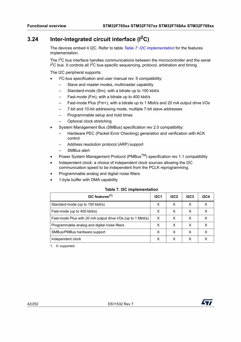
Functional overview STM32F765xx STM32F767xx STM32F768Ax STM32F769xx
42/252 DS11532 Rev 7
3.24 Inter-integrated circuit interface (I2C)
The devices embed 4 I2C. Refer to table Table 7: I2C implementation for the features implementation.
The I2C bus interface handles communications between the microcontroller and the serial I2C bus. It controls all I2C bus-specific sequencing, protocol, arbitration and timing.
The I2C peripheral supports:
• I2C-bus specification and user manual rev. 5 compatibility:
– Slave and master modes, multimaster capability
– Standard-mode (Sm), with a bitrate up to 100 kbit/s
– Fast-mode (Fm), with a bitrate up to 400 kbit/s
– Fast-mode Plus (Fm+), with a bitrate up to 1 Mbit/s and 20 mA output drive I/Os
– 7-bit and 10-bit addressing mode, multiple 7-bit slave addresses
– Programmable setup and hold times
– Optional clock stretching
• System Management Bus (SMBus) specification rev 2.0 compatibility:
– Hardware PEC (Packet Error Checking) generation and verification with ACK control
– Address resolution protocol (ARP) support
– SMBus alert
• Power System Management Protocol (PMBusTM) specification rev 1.1 compatibility
• Independent clock: a choice of independent clock sources allowing the I2C communication speed to be independent from the PCLK reprogramming.
• Programmable analog and digital noise filters
• 1-byte buffer with DMA capability
Table 7. I2C implementation
I2C features(1)
1. X: supported.
I2C1 I2C2 I2C3 I2C4
Standard-mode (up to 100 kbit/s) X X X X
Fast-mode (up to 400 kbit/s) X X X X
Fast-mode Plus with 20 mA output drive I/Os (up to 1 Mbit/s) X X X X
Programmable analog and digital noise filters X X X X
SMBus/PMBus hardware support X X X X
Independent clock X X X X
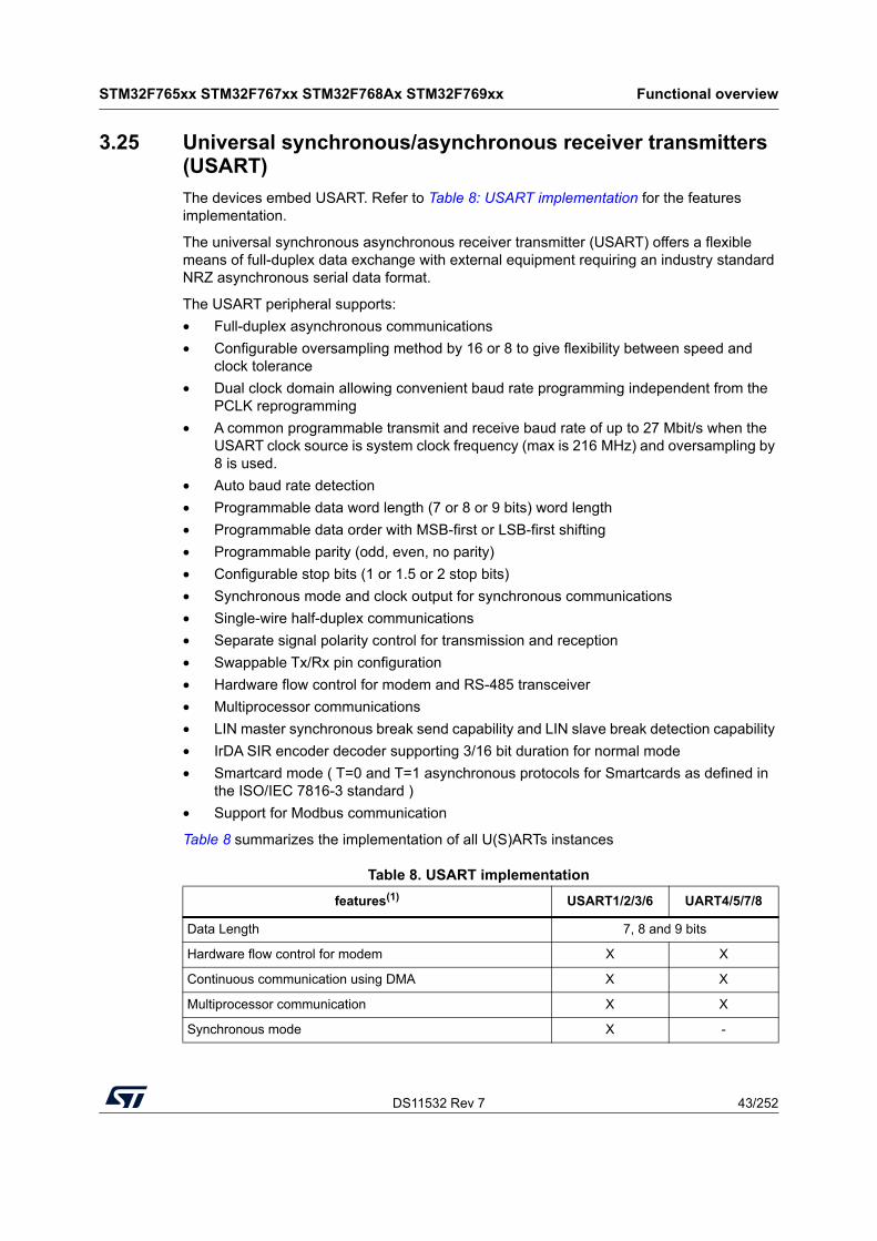
DS11532 Rev 7 43/252
STM32F765xx STM32F767xx STM32F768Ax STM32F769xx Functional overview
54
3.25 Universal synchronous/asynchronous receiver transmitters (USART)
The devices embed USART. Refer to Table 8: USART implementation for the features implementation.
The universal synchronous asynchronous receiver transmitter (USART) offers a flexible means of full-duplex data exchange with external equipment requiring an industry standard NRZ asynchronous serial data format.
The USART peripheral supports:
• Full-duplex asynchronous communications
• Configurable oversampling method by 16 or 8 to give flexibility between speed and clock tolerance
• Dual clock domain allowing convenient baud rate programming independent from the PCLK reprogramming
• A common programmable transmit and receive baud rate of up to 27 Mbit/s when the USART clock source is system clock frequency (max is 216 MHz) and oversampling by 8 is used.
• Auto baud rate detection
• Programmable data word length (7 or 8 or 9 bits) word length
• Programmable data order with MSB-first or LSB-first shifting
• Programmable parity (odd, even, no parity)
• Configurable stop bits (1 or 1.5 or 2 stop bits)
• Synchronous mode and clock output for synchronous communications
• Single-wire half-duplex communications
• Separate signal polarity control for transmission and reception
• Swappable Tx/Rx pin configuration
• Hardware flow control for modem and RS-485 transceiver
• Multiprocessor communications
• LIN master synchronous break send capability and LIN slave break detection capability
• IrDA SIR encoder decoder supporting 3/16 bit duration for normal mode
• Smartcard mode ( T=0 and T=1 asynchronous protocols for Smartcards as defined in the ISO/IEC 7816-3 standard )
• Support for Modbus communication
Table 8 summarizes the implementation of all U(S)ARTs instances
Table 8. USART implementation
features(1) USART1/2/3/6 UART4/5/7/8
Data Length 7, 8 and 9 bits
Hardware flow control for modem X X
Continuous communication using DMA X X
Multiprocessor communication X X
Synchronous mode X -
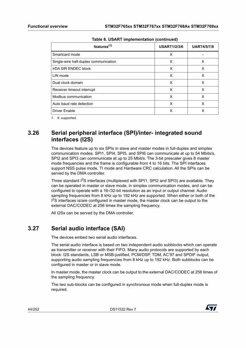
Functional overview STM32F765xx STM32F767xx STM32F768Ax STM32F769xx
44/252 DS11532 Rev 7
3.26 Serial peripheral interface (SPI)/inter- integrated sound interfaces (I2S)
The devices feature up to six SPIs in slave and master modes in full-duplex and simplex communication modes. SPI1, SPI4, SPI5, and SPI6 can communicate at up to 54 Mbits/s, SPI2 and SPI3 can communicate at up to 25 Mbit/s. The 3-bit prescaler gives 8 master mode frequencies and the frame is configurable from 4 to 16 bits. The SPI interfaces support NSS pulse mode, TI mode and Hardware CRC calculation. All the SPIs can be served by the DMA controller.
Three standard I2S interfaces (multiplexed with SPI1, SPI2 and SPI3) are available. They can be operated in master or slave mode, in simplex communication modes, and can be configured to operate with a 16-/32-bit resolution as an input or output channel. Audio sampling frequencies from 8 kHz up to 192 kHz are supported. When either or both of the I2S interfaces is/are configured in master mode, the master clock can be output to the external DAC/CODEC at 256 times the sampling frequency.
All I2Sx can be served by the DMA controller.
3.27 Serial audio interface (SAI)
The devices embed two serial audio interfaces.
The serial audio interface is based on two independent audio subblocks which can operate as transmitter or receiver with their FIFO. Many audio protocols are supported by each block: I2S standards, LSB or MSB-justified, PCM/DSP, TDM, AC’97 and SPDIF output, supporting audio sampling frequencies from 8 kHz up to 192 kHz. Both subblocks can be configured in master or in slave mode.
In master mode, the master clock can be output to the external DAC/CODEC at 256 times of the sampling frequency.
The two sub-blocks can be configured in synchronous mode when full-duplex mode is required.
Smartcard mode X -
Single-wire half-duplex communication X X
IrDA SIR ENDEC block X X
LIN mode X X
Dual clock domain X X
Receiver timeout interrupt X X
Modbus communication X X
Auto baud rate detection X X
Driver Enable X X
1. X: supported.
Table 8. USART implementation (continued)
features(1) USART1/2/3/6 UART4/5/7/8
DS11532 Rev 7 45/252
STM32F765xx STM32F767xx STM32F768Ax STM32F769xx Functional overview
54
SAI1 and SAI2 can be served by the DMA controller
3.28 SPDIFRX Receiver Interface (SPDIFRX)
The SPDIFRX peripheral, is designed to receive an S/PDIF flow compliant with IEC-60958 and IEC-61937. These standards support simple stereo streams up to high sample rate, and compressed multi-channel surround sound, such as those defined by Dolby or DTS (up to 5.1).
The main features of the SPDIFRX are the following:
• Up to 4 inputs available
• Automatic symbol rate detection
• Maximum symbol rate: 12.288 MHz
• Stereo stream from 32 to 192 kHz supported
• Supports Audio IEC-60958 and IEC-61937, consumer applications
• Parity bit management
• Communication using DMA for audio samples
• Communication using DMA for control and user channel information
• Interrupt capabilities
The SPDIFRX receiver provides all the necessary features to detect the symbol rate, and decode the incoming data stream. The user can select the wanted SPDIF input, and when a valid signal is available, the SPDIFRX re-samples the incoming signal, decodes the manchester stream, recognizes frames, sub-frames and blocks elements. It delivers to the CPU decoded data, and associated status flags.
The SPDIFRX also offers a signal named spdif_frame_sync, which toggles at the S/PDIF sub-frame rate that is used to compute the exact sample rate for clock drift algorithms.
3.29 Audio PLL (PLLI2S)
The devices feature an additional dedicated PLL for audio I2S and SAI applications. It allows to achieve error-free I2S sampling clock accuracy without compromising on the CPU performance, while using USB peripherals.
The PLLI2S configuration can be modified to manage an I2S/SAI sample rate change without disabling the main PLL (PLL) used for CPU, USB and Ethernet interfaces.
The audio PLL can be programmed with very low error to obtain sampling rates ranging from 8 KHz to 192 KHz.
In addition to the audio PLL, a master clock input pin can be used to synchronize the I2S/SAI flow with an external PLL (or Codec output).
3.30 Audio and LCD PLL (PLLSAI)
An additional PLL dedicated to audio and LCD-TFT is used for SAI1 peripheral in case the PLLI2S is programmed to achieve another audio sampling frequency (49.152 MHz or 11.2896 MHz) and the audio application requires both sampling frequencies simultaneously.
The PLLSAI is also used to generate the LCD-TFT clock.
Functional overview STM32F765xx STM32F767xx STM32F768Ax STM32F769xx
46/252 DS11532 Rev 7
3.31 SD/SDIO/MMC card host interface (SDMMC)
SDMMC host interfaces are available, that support the MultiMediaCard System Specification Version 4.2 in three different databus modes: 1-bit (default), 4-bit and 8-bit.
The interface allows data transfer at up to 50 MHz, and is compliant with the SD Memory Card Specification Version 2.0.
The SDMMC Card Specification Version 2.0 is also supported with two different databus modes: 1-bit (default) and 4-bit.
The current version supports only one SD/SDMMC/MMC4.2 card at any one time and a stack of MMC4.1 or previous.
The SDMMC can be served by the DMA controller
3.32 Ethernet MAC interface with dedicated DMA and IEEE 1588 support
The devices provide an IEEE-802.3-2002-compliant media access controller (MAC) for ethernet LAN communications through an industry-standard medium-independent interface (MII) or a reduced medium-independent interface (RMII). The microcontroller requires an external physical interface device (PHY) to connect to the physical LAN bus (twisted-pair, fiber, etc.). The PHY is connected to the device MII port using 17 signals for MII or 9 signals for RMII, and can be clocked using the 25 MHz (MII) from the microcontroller.
The devices include the following features:
• Supports 10 and 100 Mbit/s rates
• Dedicated DMA controller allowing high-speed transfers between the dedicated SRAM and the descriptors
• Tagged MAC frame support (VLAN support)
• Half-duplex (CSMA/CD) and full-duplex operation
• MAC control sublayer (control frames) support
• 32-bit CRC generation and removal
• Several address filtering modes for physical and multicast address (multicast and group addresses)
• 32-bit status code for each transmitted or received frame
• Internal FIFOs to buffer transmit and receive frames. The transmit FIFO and the receive FIFO are both 2 Kbytes.
• Supports hardware PTP (precision time protocol) in accordance with IEEE 1588 2008 (PTP V2) with the time stamp comparator connected to the TIM2 input
• Triggers interrupt when system time becomes greater than target time
DS11532 Rev 7 47/252
STM32F765xx STM32F767xx STM32F768Ax STM32F769xx Functional overview
54
3.33 Controller area network (bxCAN)
The three CANs are compliant with the 2.0A and B (active) specifications with a bit rate up to 1 Mbit/s. They can receive and transmit standard frames with 11-bit identifiers as well as extended frames with 29-bit identifiers. Each CAN has three transmit mailboxes, two receive FIFOS with 3 stages and 28 shared scalable filter banks (all of them can be used even if one CAN is used). 256 bytes of SRAM are allocated for CAN1 and CAN2. 512 bytes of SRAM are dedicated for CAN3.
3.34 Universal serial bus on-the-go full-speed (OTG_FS)
The devices embed an USB OTG full-speed device/host/OTG peripheral with integrated transceivers. The USB OTG FS peripheral is compliant with the USB 2.0 specification and with the OTG 2.0 specification. It has software-configurable endpoint setting and supports suspend/resume. The USB OTG controller requires a dedicated 48 MHz clock that is generated by a PLL connected to the HSE oscillator.
The major features are:
• Combined Rx and Tx FIFO size of 1.28 Kbytes with dynamic FIFO sizing
• Supports the session request protocol (SRP) and host negotiation protocol (HNP)
• 1 bidirectional control endpoint + 5 IN endpoints + 5 OUT endpoints
• 12 host channels with periodic OUT support
• Software configurable to OTG1.3 and OTG2.0 modes of operation
• USB 2.0 LPM (Link Power Management) support
• Battery Charging Specification Revision 1.2 support
• Internal FS OTG PHY support
• HNP/SNP/IP inside (no need for any external resistor)
For the OTG/Host modes, a power switch is needed in case bus-powered devices are connected
3.35 Universal serial bus on-the-go high-speed (OTG_HS)
The devices embed a USB OTG high-speed (up to 480 Mbit/s) device/host/OTG peripheral. The USB OTG HS supports both full-speed and high-speed operations. It integrates the transceivers for full-speed operation (12 Mbit/s) and features a UTMI low-pin interface (ULPI) for high-speed operation (480 Mbit/s). When using the USB OTG HS in HS mode, an external PHY device connected to the ULPI is required.
The USB OTG HS peripheral is compliant with the USB 2.0 specification and with the OTG 2.0 specification. It has software-configurable endpoint setting and supports suspend/resume. The USB OTG controller requires a dedicated 48 MHz clock that is generated by a PLL connected to the HSE oscillator.
The major features are:
• Combined Rx and Tx FIFO size of 4 Kbytes with dynamic FIFO sizing
• Supports the session request protocol (SRP) and host negotiation protocol (HNP)
• 8 bidirectional endpoints
• 16 host channels with periodic OUT support
Functional overview STM32F765xx STM32F767xx STM32F768Ax STM32F769xx
48/252 DS11532 Rev 7
• Software configurable to OTG1.3 and OTG2.0 modes of operation
• USB 2.0 LPM (Link Power Management) support
• Battery Charging Specification Revision 1.2 support
• Internal FS OTG PHY support
• External HS or HS OTG operation supporting ULPI in SDR mode. The OTG PHY is connected to the microcontroller ULPI port through 12 signals. It can be clocked using the 60 MHz output.
• Internal USB DMA
• HNP/SNP/IP inside (no need for any external resistor)
• for OTG/Host modes, a power switch is needed in case bus-powered devices are connected
3.36 High-definition multimedia interface (HDMI) - consumer electronics control (CEC)
The devices embed a HDMI-CEC controller that provides hardware support for the Consumer Electronics Control (CEC) protocol (Supplement 1 to the HDMI standard).
This protocol provides high-level control functions between all audiovisual products in an environment. It is specified to operate at low speeds with minimum processing and memory overhead. It has a clock domain independent from the CPU clock, allowing the HDMI-CEC controller to wakeup the MCU from Stop mode on data reception.
3.37 Digital camera interface (DCMI)
The devices embed a camera interface that can connect with camera modules and CMOS sensors through an 8-bit to 14-bit parallel interface, to receive video data. The camera interface can sustain a data transfer rate up to 54 Mbytes/s in 8-bit mode at 54 MHz. It features:
• Programmable polarity for the input pixel clock and synchronization signals
• Parallel data communication can be 8-, 10-, 12- or 14-bit
• Supports 8-bit progressive video monochrome or raw bayer format, YCbCr 4:2:2 progressive video, RGB 565 progressive video or compressed data (like JPEG)
• Supports continuous mode or snapshot (a single frame) mode
• Capability to automatically crop the image
DS11532 Rev 7 49/252
STM32F765xx STM32F767xx STM32F768Ax STM32F769xx Functional overview
54
3.38 Management Data Input/Output (MDIO) slaves
The devices embed a MDIO slave interface it includes the following features:
• 32 MDIO Registers addresses, each of which is managed using separate input and output data registers:
– 32 x 16-bit firmware read/write, MDIO read-only output data registers
– 32 x 16-bit firmware read-only, MDIO write-only input data registers
• Configurable slave (port) address
• Independently maskable interrupts/events:
– MDIO Register write
– MDIO Register read
– MDIO protocol error
• Able to operate in and wake up from STOP mode
3.39 Random number generator (RNG)
All the devices embed an RNG that delivers 32-bit random numbers generated by an integrated analog circuit.
3.40 General-purpose input/outputs (GPIOs)
Each of the GPIO pins can be configured by software as output (push-pull or open-drain, with or without pull-up or pull-down), as input (floating, with or without pull-up or pull-down) or as peripheral alternate function. Most of the GPIO pins are shared with digital or analog alternate functions. All GPIOs are high-current-capable and have speed selection to better manage internal noise, power consumption and electromagnetic emission.
The I/O configuration can be locked if needed by following a specific sequence in order to avoid spurious writing to the I/Os registers.
A fast I/O handling allows a maximum I/O toggling up to 108 MHz.
3.41 Analog-to-digital converters (ADCs)
Three 12-bit analog-to-digital converters are embedded and each ADC shares up to 16 external channels, performing conversions in the single-shot or scan mode. In scan mode, automatic conversion is performed on a selected group of analog inputs.
Additional logic functions embedded in the ADC interface allow:
• Simultaneous sample and hold
• Interleaved sample and hold
The ADC can be served by the DMA controller. An analog watchdog feature allows very precise monitoring of the converted voltage of one, some or all selected channels. An interrupt is generated when the converted voltage is outside the programmed thresholds.
To synchronize A/D conversion and timers, the ADCs could be triggered by any of TIM1, TIM2, TIM3, TIM4, TIM5, or TIM8 timer.
Functional overview STM32F765xx STM32F767xx STM32F768Ax STM32F769xx
50/252 DS11532 Rev 7
3.42 Digital filter for Sigma-Delta Modulators (DFSDM)
The devices embed one DFSDM with 4 digital filters modules and 8 external input serial channels (transceivers) or alternately 8 internal parallel inputs support. The DFSDM peripheral is dedicated to interface the external Σ∆ modulators to microcontroller and then to perform digital filtering of the received data streams (which represent analog value on Σ∆ modulators inputs). The DFSDM can also interface PDM (Pulse Density Modulation) microphones and perform PDM to PCM conversion and filtering in hardware. The DFSDM features optional parallel data stream inputs from microcontrollers memory (through DMA/CPU transfers into DFSDM). The DFSDM transceivers support several serial interface formats (to support various Σ∆ modulators). The DFSDM digital filter modules perform digital processing according user selected filter parameters with up to 24-bit final ADC resolution.
The DFSDM peripheral supports:
• 8 multiplexed input digital serial channels:
– Configurable SPI interface to connect various SD modulator(s)
– Configurable Manchester coded 1 wire interface support
– PDM (Pulse Density Modulation) microphone input support
– Maximum input clock frequency up to 20 MHz (10 MHz for Manchester coding)
– Clock output for SD modulator(s): 0..20 MHz
• Alternative inputs from 8 internal digital parallel channels (up to 16 bit input resolution):
– internal sources: device memory data streams (DMA)
• 4 digital filter modules with adjustable digital signal processing:
– Sincxfilter: filter order/type (1..5), oversampling ratio (up to 1..1024)
– integrator: oversampling ratio (1..256)
• Up to 24-bit output data resolution, signed output data format
• Automatic data offset correction (offset stored in register by user)
• Continuous or single conversion
• Start-of-conversion triggered by:
– Software trigger
– Internal timers
– External events
– Start-of-conversion synchronously with first digital filter module (DFSDM0)
• Analog watchdog feature:
– Low value and high value data threshold registers
– Dedicated configurable Sincx digital filter (order = 1..3, oversampling ratio = 1..32)
– Input from final output data or from selected input digital serial channels
– Continuous monitoring independently from standard conversion
• Short circuit detector to detect saturated analog input values (bottom and top range):
– Up to 8-bit counter to detect 1..256 consecutive 0’s or 1’s on serial data stream
– Monitoring continuously each input serial channel
• Break signal generation on analog watchdog event or on short circuit detector event
• Extremes detector:
– Storage of minimum and maximum values of final conversion data
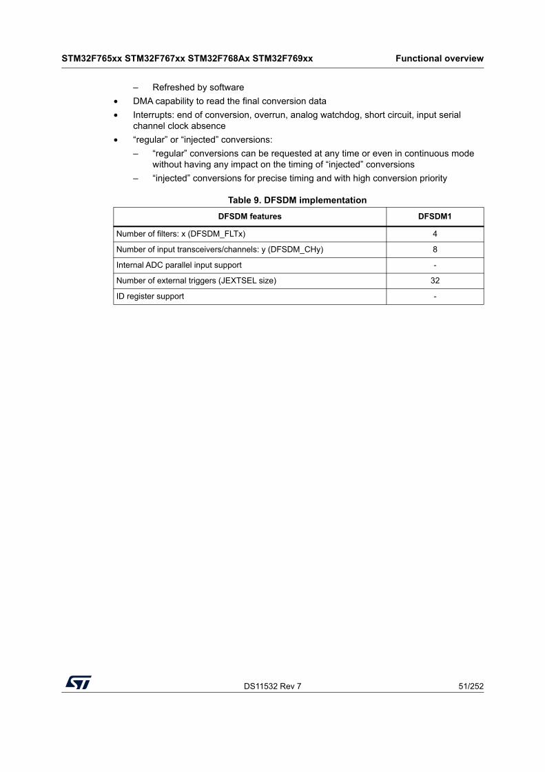
DS11532 Rev 7 51/252
STM32F765xx STM32F767xx STM32F768Ax STM32F769xx Functional overview
54
– Refreshed by software
• DMA capability to read the final conversion data
• Interrupts: end of conversion, overrun, analog watchdog, short circuit, input serial channel clock absence
• “regular” or “injected” conversions:
– “regular” conversions can be requested at any time or even in continuous mode without having any impact on the timing of “injected” conversions
– “injected” conversions for precise timing and with high conversion priority
Table 9. DFSDM implementation
DFSDM features DFSDM1
Number of filters: x (DFSDM_FLTx) 4
Number of input transceivers/channels: y (DFSDM_CHy) 8
Internal ADC parallel input support -
Number of external triggers (JEXTSEL size) 32
ID register support -
Functional overview STM32F765xx STM32F767xx STM32F768Ax STM32F769xx
52/252 DS11532 Rev 7
3.43 Temperature sensor
The temperature sensor has to generate a voltage that varies linearly with the temperature. The conversion range is between 1.7 V and 3.6 V. The temperature sensor is internally connected to the same input channel as VBAT, ADC1_IN18, which is used to convert the sensor output voltage into a digital value. When the temperature sensor and VBAT conversion are enabled at the same time, only VBAT conversion is performed.
As the offset of the temperature sensor varies from chip to chip due to process variation, the internal temperature sensor is mainly suitable for applications that detect temperature changes instead of absolute temperatures. If an accurate temperature reading is needed, then an external temperature sensor part should be used.
3.44 Digital-to-analog converter (DAC)
The two 12-bit buffered DAC channels can be used to convert two digital signals into two analog voltage signal outputs.
This dual digital Interface supports the following features:
• Two DAC converters: one for each output channel
• 8-bit or 12-bit monotonic output
• Left or right data alignment in 12-bit mode
• Synchronized update capability
• Noise-wave generation
• Triangular-wave generation
• Dual DAC channel independent or simultaneous conversions
• DMA capability for each channel
• External triggers for conversion
• Input voltage reference VREF+
Eight DAC trigger inputs are used in the device. The DAC channels are triggered through the timer update outputs that are also connected to different DMA streams.
3.45 Serial wire JTAG debug port (SWJ-DP)
The Arm SWJ-DP interface is embedded, and is a combined JTAG and serial wire debug port that enables either a serial wire debug or a JTAG probe to be connected to the target.
The debug is performed using 2 pins only instead of 5 required by the JTAG (JTAG pins could be re-use as GPIO with alternate function): the JTAG TMS and TCK pins are shared with SWDIO and SWCLK, respectively, and a specific sequence on the TMS pin is used to switch between JTAG-DP and SW-DP.
3.46 Embedded Trace Macrocell™
The Arm embedded trace Macrocell provides a greater visibility of the instruction and data flow inside the CPU core by streaming compressed data at a very high rate from the STM32F76xxx through a small number of ETM pins to an external hardware trace port analyzer (TPA) device. The TPA is connected to a host computer using USB, Ethernet, or
DS11532 Rev 7 53/252
STM32F765xx STM32F767xx STM32F768Ax STM32F769xx Functional overview
54
any other high-speed channel. Real-time instruction and data flow activity can be recorded and then formatted for display on the host computer that runs the debugger software. TPA hardware is commercially available from common development tool vendors.
The Embedded Trace Macrocell operates with third party debugger software tools.
3.47 DSI Host (DSIHOST)
The DSI Host is a dedicated peripheral for interfacing with MIPI® DSI compliant displays. It includes a dedicated video interface internally connected to the LTDC and a generic APB interface that can be used to transmit information to the display.
These interfaces are as follows:
• LTDC interface:
– Used to transmit information in Video mode, in which the transfers from the host processor to the peripheral take the form of a real-time pixel stream (DPI).
– Through a customized for mode, this interface can be used to transmit information in full bandwidth in the Adapted Command mode (DBI).
• APB slave interface:
– Allows the transmission of generic information in Command mode, and follows a proprietary register interface.
– Can operate concurrently with either LTDC interface in either Video mode or Adapted Command mode.
• Video mode pattern generator:
– Allows the transmission of horizontal/vertical color bar and D-PHY BER testing pattern without any kind of stimuli.
The DSI Host main features:
• Compliant with MIPI® Alliance standards
• Interface with MIPI® D-PHY
• Supports all commands defined in the MIPI® Alliance specification for DCS:
– Transmission of all Command mode packets through the APB interface
– Transmission of commands in low-power and high-speed during Video mode
• Supports up to two D-PHY data lanes
• Bidirectional communication and escape mode support through data lane 0
• Supports non-continuous clock in D-PHY clock lane for additional power saving
• Supports Ultra Low-power mode with PLL disabled
• ECC and Checksum capabilities
• Support for End of Transmission Packet (EoTp)
• Fault recovery schemes
• 3D transmission support
• Configurable selection of system interfaces:
– AMBA APB for control and optional support for Generic and DCS commands
– Video Mode interface through LTDC
– Adapted Command mode interface through LTDC
• Independently programmable Virtual Channel ID in
Functional overview STM32F765xx STM32F767xx STM32F768Ax STM32F769xx
54/252 DS11532 Rev 7
– Video mode
– Adapted Command mode
– APB Slave
Video Mode interfaces features:
• LTDC interface color coding mappings into 24-bit interface:
– 16-bit RGB, configurations 1, 2, and 3
– 18-bit RGB, configurations 1 and 2
– 24-bit RGB
• Programmable polarity of all LTDC interface signals
• Maximum resolution is limited by available DSI physical link bandwidth:
– Number of lanes: 2
– Maximum speed per lane: 500 Mbps1Gbps
Adapted interface features
Support for sending large amounts of data through the memory_write_start(WMS) and memory_write_continue(WMC) DCS commands
• LTDC interface color coding mappings into 24-bit interface:
– 16-bit RGB, configurations 1, 2, and 3
– 18-bit RGB, configurations 1 and 2
– 24-bit RGB
Video mode pattern generator:
• Vertical and horizontal color bar generation without LTDC stimuli
• BER pattern without LTDC stimuli
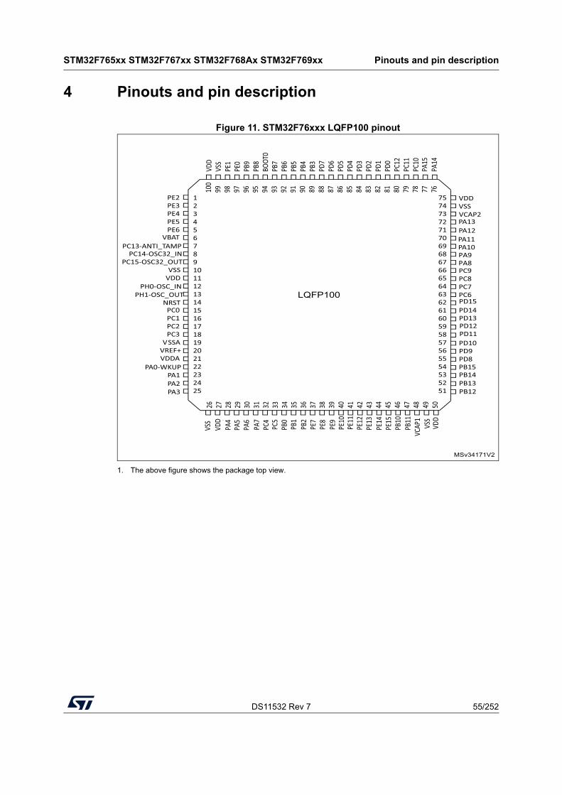
DS11532 Rev 7 55/252
STM32F765xx STM32F767xx STM32F768Ax STM32F769xx Pinouts and pin description
102
4 Pinouts and pin description
Figure 11. STM32F76xxx LQFP100 pinout
1. The above figure shows the package top view.
100
99 98 97 96 95 94 93 92 91 90 89 88 87 86 85 84 83 82 81 80 79 78 77 76
12345678910111213141516171819202122232425
75747372717069686766656463626160595857565554535251
PE2PE3PE4PE5PE6
PC14-OSC32_INPC15-OSC32_OUT
VSSVDD
PH0-OSC_IN
PC0PC1PC2PC3
VSSAVREF+VDDA
VDDVSSVCAP2
PC9PC8PC7PC6
VSS
VDD
PA4
PB1
PB2
PE7
PE8
PE9
VCAP
1
VDD
VDD
VSS
PD7
PD
6
PD5
PD
4
PD3
PD
2
PD1
PD
0
PC12
PC11
PC10
26 27 28 29 30 31 32 33 34 35 36 37 38 39 40 41 42 43 44 45 46 47 48 49 50
MSv34171V2
LQFP100
PC13-ANTI_TAMP
PH1-OSC_OUT
PA0-WKUPPA1PA2PA3
PA5
PA6
PA7
PC4
PB0
PC5
PE13
PE14
PE15
PB10
PB11
PE10
PE12
PE11
VSS
PD12PD11
PD8PB15PB14PB13PB12
PD9PD10
PD13PD14PD15
PA9PA8
PA10PA11PA12PA13
PA15
PA14
PE1
PE0
PB9
PB8
BOOT
0 PB
7 PB
6 PB
5 PB
4PB
3
VBAT
NRST
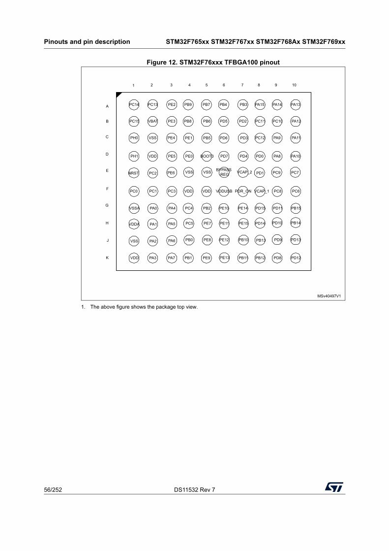
Pinouts and pin description STM32F765xx STM32F767xx STM32F768Ax STM32F769xx
56/252 DS11532 Rev 7
Figure 12. STM32F76xxx TFBGA100 pinout
1. The above figure shows the package top view.
MSv40497V1
A
B
E
D
C
F
G
H
J
K
PC14
NRST
PH1
PH0
PC15
VDDA
VSS
VDD
PC13
VSS
VBAT
VDD
PC2
PA1
PA2
PA3
PE2
PE4
PE3
PE5
PE6
PA5
PA6
PA7
PB9
PB8
PB1
PB7
PB6
PE9
PB4
PD5
PB3
PD2
PB11
PA15
PC11
PC12
PD1
PD0
PD14
PB13
PB12
PA14
PC10
PA9
PA8
PC9
PD10
PD9
PD8
PA13
PA12
PA11
PA10
PC7
PB14
PD13
PD12
2 3 4 5 6 7 8 9 101
PC0
VSSA
PC1
PA0
PC3
PA4
VDD
PC4
VDD
PB2
VDDUSB
PE10
PDR_ON
PE14
VCAP_1
PD15
PC8
PD11
PC6
PB15
PC5 PE7 PE11 PE15
PE1
PE0
PB5
BOOT0
PD6
PD7
PD3
PD4
VSS VSS BYPASS-REG VCAP_2
PB0 PE8 PE12 PB10
PE13
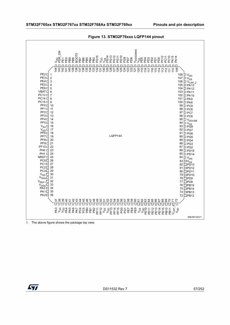
DS11532 Rev 7 57/252
STM32F765xx STM32F767xx STM32F768Ax STM32F769xx Pinouts and pin description
102
Figure 13. STM32F76xxx LQFP144 pinout
1. The above figure shows the package top view.
VD
DP
DR
_ON
PE
1P
E0
PB
9P
B8
BO
OT0
PB
7P
B6
PB
5P
B4
PB
3P
G15
VD
DV
SS
PG
14P
G13
PG
12P
G11
PG
10P
G9
PD
7P
D6
VD
DS
DM
MC
VS
SP
D5
PD
4P
D3
PD
2P
D1
PD
0P
C12
PC
11P
C10
PA15
PA14
PE2 VDDPE3 VSSPE4PE5 PA13PE6 PA12
VBAT PA11PC13 PA10PC14 PA9PC15 PA8
PF0 PC9PF1 PC8PF2 PC7PF3 PC6PF4 VDDUSBPF5 VSSVSS PG8VDD PG7PF6 PG6PF7 PG5PF8 PG4PF9 PG3
PF10 PG2PH0 PD15PH1 PD14
NRST VDDPC0 VSSPC1 PD13PC2 PD12PC3 PD11
VSSAPD10VDDPD9
VREF+ PD8VDDA PB15PA0 PB14PA1 PB13PA2 PB12
PA3
VS
SV
DD
PA4
PA5
PA6
PA7
PC
4P
C5
PB
0P
B1
PB
2P
F11
PF1
2
VD
DP
F13
PF1
4P
F15
PG
0P
G1
PE
7P
E8
PE
9V
SS
VD
DPE
10PE
11PE
12PE
13PE
14PE
15PB
10PB
11
VD
D
144
143
142
141
140
139
138
137
136
135
134
133
132
131
130
129
128
127
126
125
124
123
122
121
109
12345678910111213141516171819202122232425
108107106105104103102101100
99989796959493929190898887868584
37 38 39 40 41 42 43 44 45 46 47 48 49 50 51 52 53 54 55 56 57 58 59 60 72
LQFP14412
011
911
811
711
611
511
411
311
211
111
0
61 62 63 64 65 66 67 68 69 70 71
2627282930313233343536
8382818079787776757473
VCAP_2
VS
S
MS39132V1
VC
AP
_1
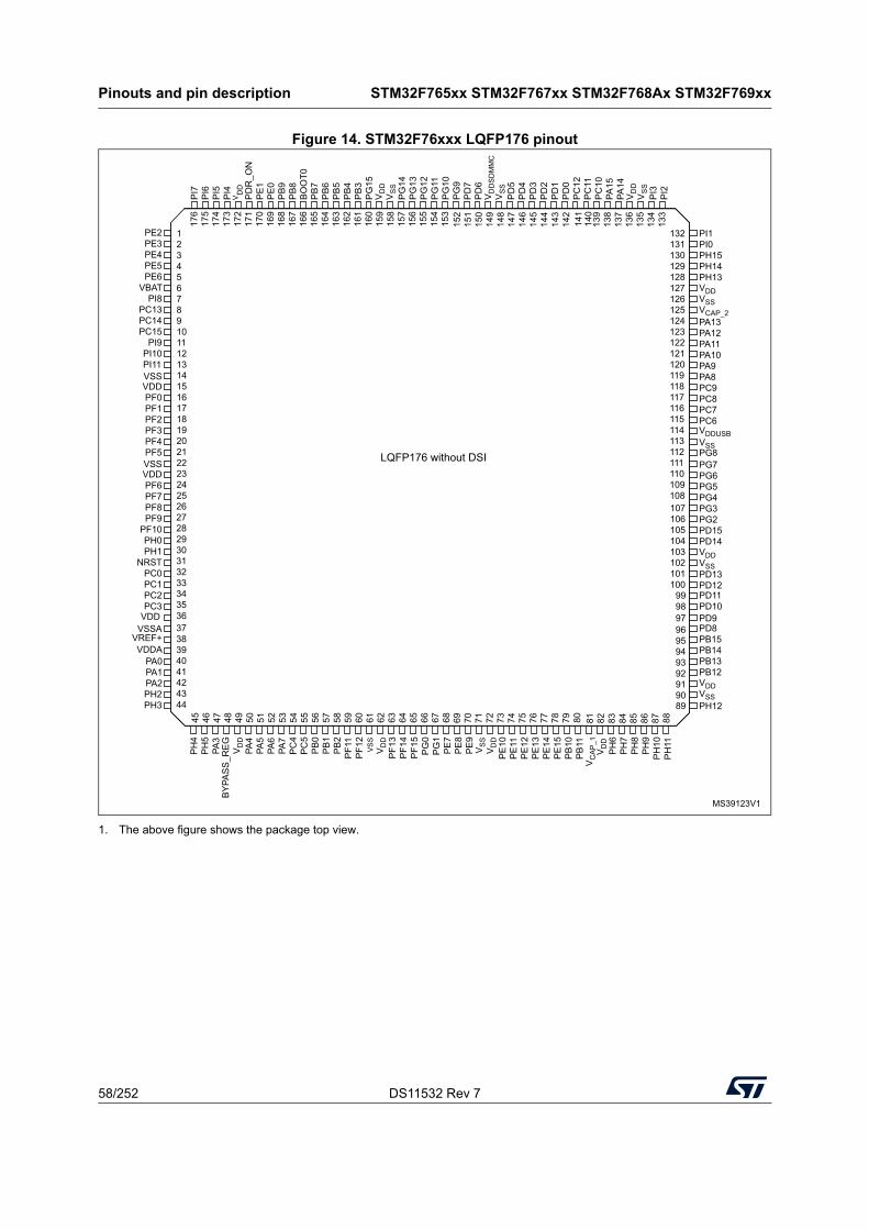
Pinouts and pin description STM32F765xx STM32F767xx STM32F768Ax STM32F769xx
58/252 DS11532 Rev 7
Figure 14. STM32F76xxx LQFP176 pinout
1. The above figure shows the package top view.
MS39123V1
PD
R_O
NV
DD
PE
1P
E0
PB
9P
B8
BO
OT0
PB
7P
B6
PB
5P
B4
PB
3P
G15
VD
DV
SS
PG
14P
G13
PG
12P
G11
PG
10P
G9
PD
7P
D6
VD
DS
DM
MC
VS
SP
D5
PD
4P
D3
PD
2P
D1
PD
0P
C12
PC
11P
C10
PI7
PI6
PE2
VDD
PE3
VSS
PE4PE5
PA13
PE6
PA12
VBAT
PA11
PI8
PA10
PC14
PA9
PC15
PA8
PF0PC9
PF1PC8
PF2PC7
PF3PC6
PF4VDDUSB
PF5VSSPG8PG7
PF6PG6
PF7PG5
PF8PG4
PF9PG3
PF10PG2
PH0PD15
PH1PD14
NRSTVDD
PC0VSS
PC1PD13
PC2PD12
PC3PD11PD10PD9
VREF+PD8PB15
PA0PB14
PA1PB13
PA2PB12
PA3
BY
PAS
S_R
EG
VD
DPA
4PA
5PA
6PA
7P
C4
PC
5P
B0
PB
1P
B2
PF1
1P
F12
VS
SV
DD
PF1
3P
F14
PF1
5P
G0
PG
1P
E7
PE
8P
E9
VS
SV
DD
PE
10P
E11
PE
12P
E13
PE
14P
E15
PB
10P
B11
VC
AP
_1V
DD
176
175
174
173
172
171
170
169
168
167
166
165
164
163
162
161
160
159
158
157
156
155
154
153
141
12345678910111213141516171819202122232425
132131130129128127126125124123122121120119118117116115114113112111110109108
45 46 47 48 49 50 51 52 53 54 55 56 57 58 59 60 61 62 63 64 65 66 67 68 80
LQFP176 without DSI15
215
115
014
914
814
714
614
514
414
314
2
69 70 71 72 73 74 75 76 77 78 79
2627282930313233343536
107106105104103102101100
9998
89
VCAP_2
PI4
PA15
PA14
VD
DV
SS
PI3
PI2
PI5
140
139
138
137
136
135
134
133
PH
4P
H5
PH
6P
H7
PH
8P
H9
PH
10P
H11
8881 82 83 84 85 86 87
PI1PI0PH15PH14PH13
VDDVSSPH12
96959493929190
973738394041424344
PC13
PI9PI10PI11VSS
PH2PH3
VDD
VSSVDD
VDDVSSA
VDDA
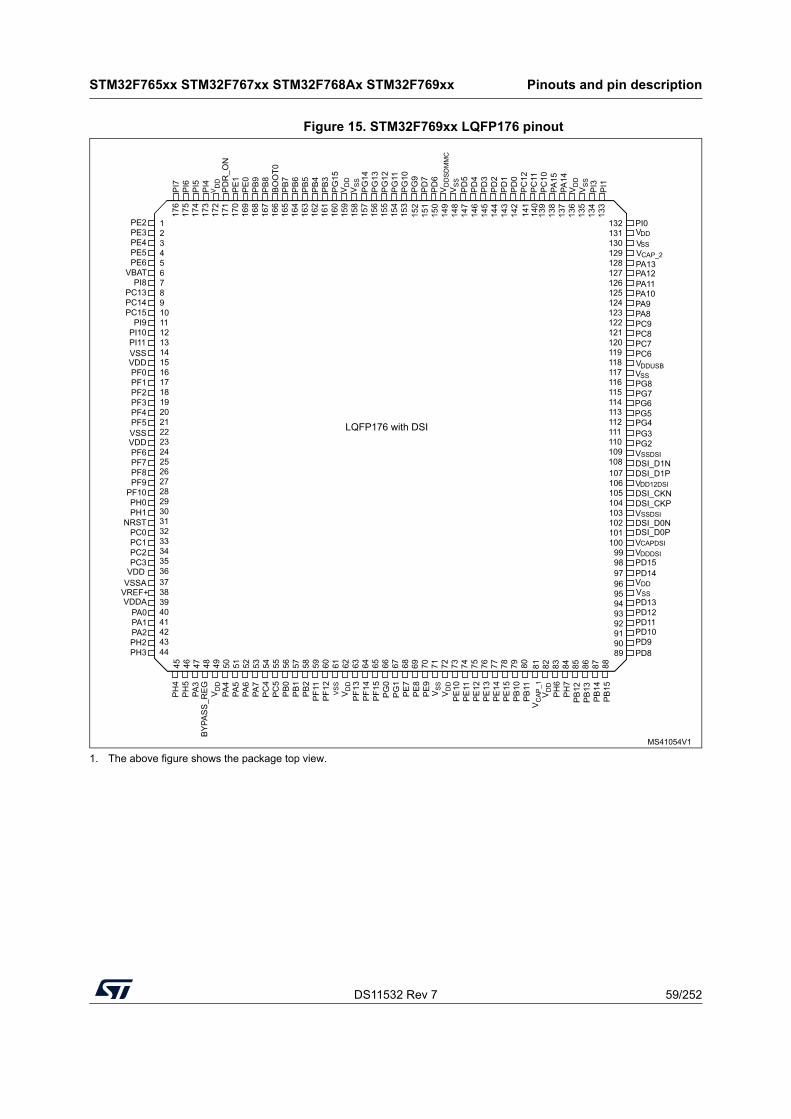
DS11532 Rev 7 59/252
STM32F765xx STM32F767xx STM32F768Ax STM32F769xx Pinouts and pin description
102
Figure 15. STM32F769xx LQFP176 pinout
1. The above figure shows the package top view.
MS41054V1
PD
R_O
NV
DD
PE
1P
E0
PB
9P
B8
BO
OT0
PB
7P
B6
PB
5P
B4
PB
3P
G15
VD
DV
SS
PG
14P
G13
PG
12P
G11
PG
10P
G9
PD
7P
D6
VD
DS
DM
MC
VS
SP
D5
PD
4P
D3
PD
2P
D1
PD
0P
C12
PC
11P
C10
PI7
PI6
PE2
VDDPE3 VSSPE4
PE5
PA9
PE6
PA8
VBAT
PC9
PI8
PC8
PC14
PC7
PC15
PC6
PF0
PA10
PF1V
PF2PG8
PF3PG7
PF4
VDDUSB
PF5
V
PG4PG3
PF6PG2
PF7V
PF8DSI_D1N
PF9DSI_D1P
PF10V
PH0DSI_CKN
PH1DSI_CKP
NRST
VDD
PC0 DSI_D0PPC1 VPC2
PG5
PC3VPD15PD14
VREF+
PA0PD13
PA1PD12
PA2PD11
PA3
BY
PAS
S_R
EG
VD
DPA
4PA
5PA
6PA
7P
C4
PC
5P
B0
PB
1P
B2
PF1
1P
F12
VS
SV
DD
PF1
3P
F14
PF1
5P
G0
PG
1P
E7
PE
8P
E9
VS
SV
DD
PE
10P
E11
PE
12P
E13
PE
14P
E15
PB
10P
B11
VC
AP
_1V
DD
176
175
174
173
172
171
170
169
168
167
166
165
164
163
162
161
160
159
158
157
156
155
154
153
141
12345678910111213141516171819202122232425
132131130129128127126125124123122121120119118117116115114113112111110109108
45 46 47 48 49 50 51 52 53 54 55 56 57 58 59 60 61 62 63 64 65 66 67 68 80
LQFP176 with DSI15
215
115
014
914
814
714
614
514
414
314
2
69 70 71 72 73 74 75 76 77 78 79
2627282930313233343536
107106105104103102101100
9998
89
VCAP_2
PI4
PA15
PA14
VD
DV
SS
PI3
PI1
PI5
140
139
138
137
136
135
134
133
PH
4P
H5
PH
6P
H7
PB
12P
B13
PB
14P
B15
8881 82 83 84 85 86 87
PI0
PA12PA13
PD10PD9PD8
96959493929190
973738394041424344
PC13
PI9PI10PI11VSS
PH2PH3
VDD
VSSVDD
VDDVSSA
VDDASS
DSI_D0N
PG6
SS
PA11
SSDSI
DD12DSI
DDDSI
VSSDSI
CAPDSI
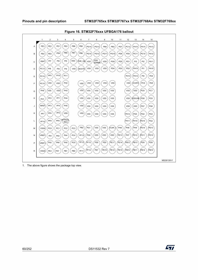
Pinouts and pin description STM32F765xx STM32F767xx STM32F768Ax STM32F769xx
60/252 DS11532 Rev 7
Figure 16. STM32F76xxx UFBGA176 ballout
1. The above figure shows the package top view.
MS39130V1
1 2 3 9 10 11 12 13 14 15
A PE3 PE2 PE1 PE0 PB8 PB5 PG14 PG13 PB4 PB3 PD7 PC12 PA15 PA14 PA13
B PE4 PE5 PE6 PB9 PB7 PB6 PG15 PG12 PG11 PG10 PD6 PD0 PC11 PC10 PA12
C VBAT PI7 PI6 PI5 PDR_ONVDD VDD VDD SDMMC VDD PG9 PD5 PD1 PI3 PI2 PA11
D PC13 PI8 PI9 PI4 BOOT0 VSS VSS VSS PD4 PD3 PD2 PH15 PI1 PA10
E PC14 PF0 PI10 PI11 PH13 PH14 PI0 PA9
F PC15 VSS VDD PH2 VSS VSS VSS VSS VSS VSS VCAP2 PC9 PA8
G PH0 VSS VDD PH3 VSS VSS VSS VSS VSS VSS VDD PC8 PC7
H PH1 PF2 PF1 PH4 VSS VSS VSS VSS VSS VSS VDDUSB PG8 PC6
J NRST PF3 PH5 VSS VSS VSS VSS VSS VDD VDD PG7 PG6
K PF7 PF6
PF4
VDD VSS VSS VSS VSS VSS PH12 PG5 PG4 PG3
L PF10 PF9
PF5
BYPASS_REG PH11 PH10 PD15 PG2
M VSSA PC0
PF8
PC1 PC2 PC3 PB2 PG1 VSS VSS VCAP_1 PH6 PH8 PH9 PD14 PD13
N VREF- PA0 PA4 PC4 PF13 PG0 VDD VDD VDD PE13 PH7 PD12 PD11 PD10
P VREF+ PA2 PA6 PA5 PC5 PF12 PF15 PE8 PE9 PE11 PE14 PB12 PB13 PD9 PD8
R VDDA PA3 PA7 PB1 PB0 PF11 PF14 PE7 PE10 PE12 PE15 PB10 PB11 PB14 PB15
VSS
4 5 6 7 8
PA1
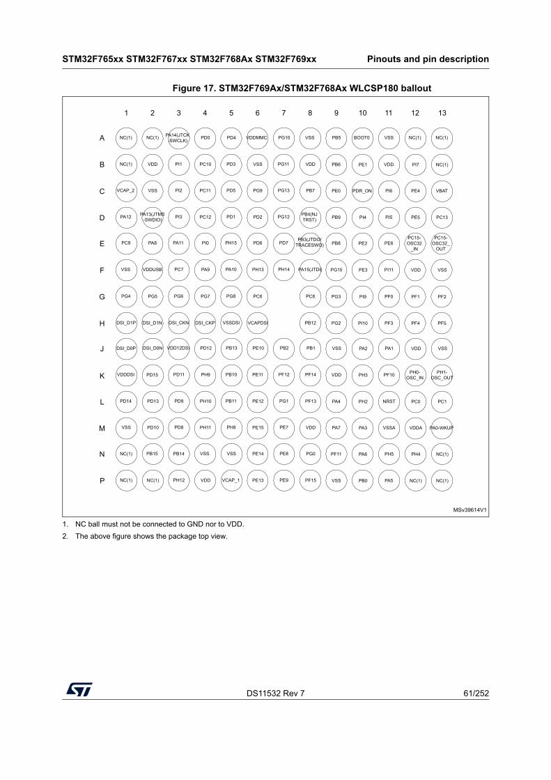
DS11532 Rev 7 61/252
STM32F765xx STM32F767xx STM32F768Ax STM32F769xx Pinouts and pin description
102
Figure 17. STM32F769Ax/STM32F768Ax WLCSP180 ballout
1. NC ball must not be connected to GND nor to VDD.
2. The above figure shows the package top view.
MSv39614V1
A
B
C
D
E
F
G
H
J
K
L
M
N
P
PA0-WKUP
121110987654321
NC(1)VSSBOOT0PB5VSSPG10VDDMMCPD4PD0PA14(JTCK-SWCLK)NC(1)NC(1)
PI7VDDPE1PB6VDDPG11VSSPD3PC10PI1VDDNC(1)
PE4PI6PDR_ONPE0PB7PG13PG9PD5PC11PI2VSSVCAP_2
PE5PI5PI4PB9PB4(NJTRST)PG12PD2PD1PC12PI3PA13(JTMS
-SWDIO)PA12
PC15-OSC32
_INPE6PE2PB8
PB3(JTDO/TRACESWO)PD7PD6PH15PI0PA11PA8PC9
VDDPI11PE3PG15PA15(JTDI)PH14PH13PA10PA9PC7VDDUSBVSS
PF1PF0PI9PG3PC8PC6PG8PG7PG6PG5PG4
PF4PF3PI10PG2PB12VCAPDSIVSSDSIDSI_CKPDSI_CKNDSI_D1NDSI_D1P
VDDPA1PA2VSSPB1PB2PE10PB13PD12VDD12DSIDSI_D0NDSI_D0P
PH0-OSC_INPF10PH3VDDPF14PF12PE11PB10PH9PD11PD15VDDDSI
PC0NRSTPH2PA4PF13PG1PE12PB11PH10PD9PD13PD14
VDDAVSSAPA3PA7VDDPE7PE15PH8PH11PD8PD10VSS
PH4PH5PA6PF11PG0PE8PE14VSSPB14PB15NC(1) VSS
NC(1)PA5PB0VSSPF15PE9PE13VCAP_1VDDPH12NC(1)NC(1)
NC(1)
NC(1)
VBAT
PC13
PC15-OSC32_
OUT
VSS
PF2
PF5
VSS
PH1-OSC_OUT
PC1
NC(1)
NC(1)
13
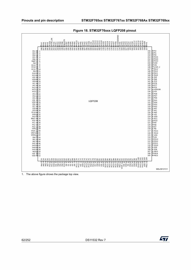
Pinouts and pin description STM32F765xx STM32F767xx STM32F768Ax STM32F769xx
62/252 DS11532 Rev 7
Figure 18. STM32F76xxx LQFP208 pinout
1. The above figure shows the package top view.
MSv39131V1
PI7
PI6
PI5
PI4
VDD
VSS
PE1
PE0
PB9
PB8
PB7
PB6
PB5
PB4
PB3
PG15
PK7
PK6
PK5
PK4
PK3
VDD
VSS
PG14
PG13
PG12
PG11
PG10
PG9
PJ15
PJ14
PJ13
PJ12
PD7
PD6
VDDS
DMM
CVS
SPD
5PD
4PD
3PD
2PD
1PD
0PC
12PC
11PC
10PA
15PA
14VD
DPI
3
1 1562 1553 1544 1535 1526 1517 1508 1499 148
10 14711 14612 14513 14414 14315 14216 14117 14018 13919 13820 13721 13622232425 LQFP208262728293031323334353637383940414243444546474849505152
53 54 55 56 57 58 59 60 61 62 63 64 65 66 67 68 69 70 71 72 73 74 75 76 77 78 79 80 81 82 83 84 85 86 87 88 89 90 91 92 93 94 95 96 97 98 99 100
101
102
103
104
PE2PE3PE4PE5PE6
VBATPI8
PC13PC14PC15
PI9PI10PI11VSSVDDPF0PF1PF2PI12PI13PI14PF3PF4PF5VSSVDDPF6PF7PF8PF9
PF10PH0PH1
NRSTPC0PC1PC2PC3VDD
VSSAVREF+VDDA
PA0PA1PA2PH2PH3PH4PH5PA3VSSVDD
PI2PI1PI0PH15PH14PH13VDDVSSVCAP_2PA13PA12PA11PA10PA9PA8PC9PC8PC7PC6VDDUSBVSSPG8PG7PG6PG5PG4PG3PG2PK2PK1PK0VSSVDDPJ11PJ10PJ9PJ8PJ7PJ6PD15PD14VDDVSSPD13PD12PD11PD10PD9PD8PB15PB14PB13
135134133132131130129128127126125124123122121120119118117116115114113112111110109108107106105
PDR_
ON
BOO
T0
208
207
206
205
204
203
202
201
200
199
198
197
196
195
194
193
192
191
190
189
188
187
186
185
184
183
182
181
180
179
178
177
176
175
174
173
172
171
170
169
168
167
166
165
164
163
162
161
160
159
158
157
PA4
PA5
PA6
PA7
PC4
PC5
VDD
VSS
PB0
PB1
PB2
PI15 PJ0
PJ1
PJ2
PJ3
PJ4
PF11
PF12
VSS
VDD
PF13
PF14
PF15
PG0
PG1
PE7
PE8
PE9
VSS
VDD
PE10
PE11
PE12
PE13
PE14
PE15
PB10
PB11
VCAP
_1VS
SVD
DPJ
5PH
6PH
7PH
8PH
9PH
10PH
11PH
12VD
DPB
12
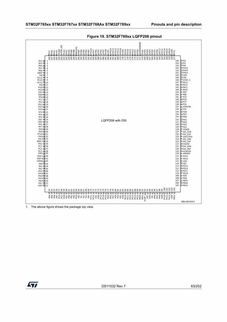
DS11532 Rev 7 63/252
STM32F765xx STM32F767xx STM32F768Ax STM32F769xx Pinouts and pin description
102
Figure 19. STM32F769xx LQFP208 pinout
1. The above figure shows the package top view.
MSv39124V1
PI7
PI6
PI5
PI4
VDD
VSS
PE1
PE0
PB9
PB8
PB7
PB6
PB5
PB4
PB3
PG15
PK7
PK6
PK5
PK4
PK3
VDD
VSS
PG14
PG13
PG12
PG11
PG10
PG9
PJ15
PJ14
PJ13
PJ12
PD7
PD6
VDDS
DMM
CVS
SPD
5PD
4PD
3PD
2PD
1PD
0PC
12PC
11PC
10PA
15PA
14VD
DPI
3
1 1562 1553 1544 1535 1526 1517 1508 1499 148
10 14711 14612 14513 14414 14315 14216 14117 14018 13919 13820 13721 13622232425 LQFP208 with DSI262728293031323334353637383940414243444546474849505152
53 54 55 56 57 58 59 60 61 62 63 64 65 66 67 68 69 70 71 72 73 74 75 76 77 78 79 80 81 82 83 84 85 86 87 88 89 90 91 92 93 94 95 96 97 98 99 100
101
102
103
104
PE2PE3PE4PE5PE6
VBATPI8
PC13PC14PC15
PI9PI10PI11VSSVDDPF0PF1PF2PI12PI13PI14PF3PF4PF5VSSVDDPF6PF7PF8PF9
PF10PH0PH1
NRSTPC0PC1PC2PC3VDD
VSSAVREF+VDDA
PA0PA1PA2PH2PH3PH4PH5PA3VSSVDD
PI2PI1PI0PH15PH14PH13VDDVSSVCAP_2PA13PA12PA11PA10PA9PA8PC9PC8PC7PC6VDDUSBVSSPG8PG7PG6PG5PG4PG3PG2VSSDSIDSI_D1NDSI_D1PVDD12DSIDSI_CKNDSI_CKPVSSDSIDSI_D0NDSI_D0PVCAPDSIVDDDSIPD15PD14VDDVSSPD13PD12PD11PD10PD9PD8PB15PB14PB13
135134133132131130129128127126125124123122121120119118117116115114113112111110109108107106105
PDR_
ON
BOO
T0
208
207
206
205
204
203
202
201
200
199
198
197
196
195
194
193
192
191
190
189
188
187
186
185
184
183
182
181
180
179
178
177
176
175
174
173
172
171
170
169
168
167
166
165
164
163
162
161
160
159
158
157
PA4
PA5
PA6
PA7
PC4
PC5
VDD
VSS
PB0
PB1
PB2
PI15 PJ0
PJ1
PJ2
PJ3
PJ4
PF11
PF12
VSS
VDD
PF13
PF14
PF15
PG0
PG1
PE7
PE8
PE9
VSS
VDD
PE10
PE11
PE12
PE13
PE14
PE15
PB10
PB11
VCAP
_1VS
SVD
DPJ
5PH
6PH
7PH
8PH
9PH
10PH
11PH
12VD
DPB
12
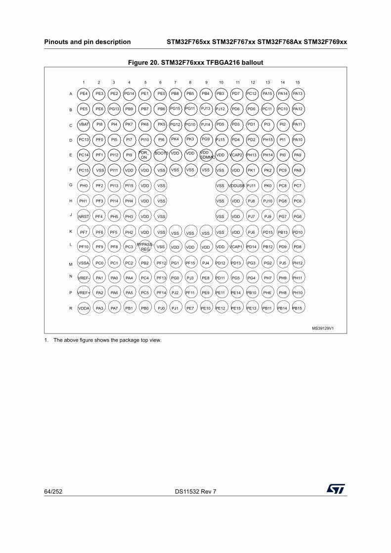
Pinouts and pin description STM32F765xx STM32F767xx STM32F768Ax STM32F769xx
64/252 DS11532 Rev 7
Figure 20. STM32F76xxx TFBGA216 ballout
1. The above figure shows the package top view.
MS39129V1
1 2 3 4 5 6 7 8 9 10 11 12 13 14 15
A PE4 PE3 PE2 PG14 PE1 PE0 PB8 PB5 PB4 PB3 PD7 PC12 PA15 PA14 PA13
B PE5 PE6 PG13 PB9 PB7 PB6 PG15 PG11 PJ13 PJ12 PD6 PD0 PC11 PC10 PA12
C VBAT PI8 PI4 PK7 PK6 PK5 PG12 PG10 PJ14 PD5 PD3 PD1 PI3 PI2 PA11
D PC13 PF0 PI5 PI7 PI10 PI6 PK4 PK3 PG9 PJ15 PD4 PD2 PH15 PI1 PA10
E PC14 PF1 PI12 PI9 PDR_ON
BOOT0 VDD VDD VDD SDMMC VDD VCAP2 PH13 PH14 PI0 PA9
F PC15 VSS PI11 VDD VDD VSS VSS VDD PK1 PK2 PC9 PA8
G PH0 PF2 PI13 PI15 VDD VSS VDDUSB PJ11 PK0 PC8 PC7
H PH1 PI14 PH4 VDD VSS VSS VDD PJ8 PJ10 PG8 PC6
J NRST PF4 PH5 PH3 VDD VSS VSS VDD PJ7 PJ9 PG7 PG6
K PF7 PF6 PF5 PH2 VDD VSS VSS VSS VSS VSS VDD PJ6 PD15 PB13 PD10
L PF10 PF9 PF8 PC3 BYPASS-REG VSS VDD VDD VDD VDD VCAP1 PD14 PB12 PD9 PD8
M VSSA PC0 PC1 PC2 PB2 PF12 PG1 PF15 PJ4 PD12 PD13 PG3 PG2 PJ5 PH12
N VREF- PA1 PA0 PA4 PC4 PF13 PG0 PJ3 PE8 PD11 PG5 PG4 PH7 PH9 PH11
VREF+ PA2 PA6 PA5 PC5 PF14 PJ2 PF11 PE9 PE11 PE14 PB10 PH6 PH8 PH10
PA3 PA7 PB1 PB0 PJ0 PJ1 PE7 PE10 PE12 PE15 PE13 PB11 PB14 PB15
VSS
PF3
P
R VDDA
VSS VSS VSS
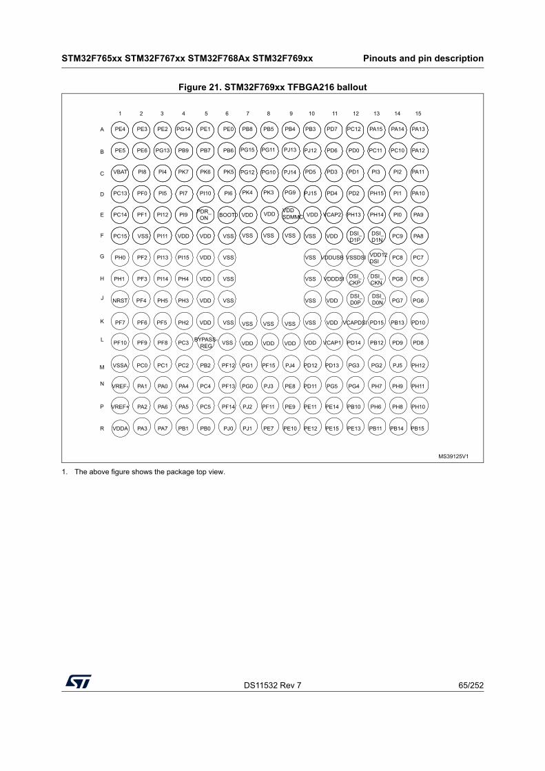
DS11532 Rev 7 65/252
STM32F765xx STM32F767xx STM32F768Ax STM32F769xx Pinouts and pin description
102
Figure 21. STM32F769xx TFBGA216 ballout
1. The above figure shows the package top view.
MS39125V1
1 2 3 4 5 6 7 8 9 10 11 12 13 14 15
A PE4 PE3 PE2 PG14 PE1 PE0 PB8 PB5 PB4 PB3 PD7 PC12 PA15 PA14 PA13
B PE5 PE6 PG13 PB9 PB7 PB6 PG15 PG11 PJ13 PJ12 PD6 PD0 PC11 PC10 PA12
C VBAT PI8 PI4 PK7 PK6 PK5 PG12 PG10 PJ14 PD5 PD3 PD1 PI3 PI2 PA11
D PC13 PF0 PI5 PI7 PI10 PI6 PK4 PK3 PG9 PJ15 PD4 PD2 PH15 PI1 PA10
E PC14 PF1 PI12 PI9 PDR_ON BOOT0 VDD VDD
VDD SDMMC VDD VCAP2 PH13 PH14 PI0 PA9
F PC15 VSS PI11 VDD VDD VSS VSS VDD DSI_ D1P
DSI_ D1N
PC9 PA8
G PH0 PF2 PI13 PI15 VDD VSS VDDUSB VSSDSI VDD12DSI
PC8 PC7
H PH1 PI14 PH4 VDD VSS VSS VDDDSI DSI_ CKP
DSI_CKN
PG8 PC6
J NRST PF4 PH5 PH3 VDD VSS VSS VDDDSI_D0P
DSI_D0N PG7 PG6
K PF7 PF6 PF5 PH2 VDD VSS VSS VSS VSS VSS VDD VCAPDSI PD15 PB13 PD10
L PF10 PF9 PF8 PC3 BYPASS-REG VSS VDD VDD VDD VDD VCAP1 PD14 PB12 PD9 PD8
M VSSA PC0 PC1 PC2 PB2 PF12 PG1 PF15 PJ4 PD12 PD13 PG3 PG2 PJ5 PH12
N VREF- PA1 PA0 PA4 PC4 PF13 PG0 PJ3 PE8 PD11 PG5 PG4 PH7 PH9 PH11
VREF+ PA2 PA6 PA5 PC5 PF14 PJ2 PF11 PE9 PE11 PE14 PB10 PH6 PH8 PH10
PA3 PA7 PB1 PB0 PJ0 PJ1 PE7 PE10 PE12 PE15 PE13 PB11 PB14 PB15
VSS
PF3
P
R VDDA
VSS VSS VSS
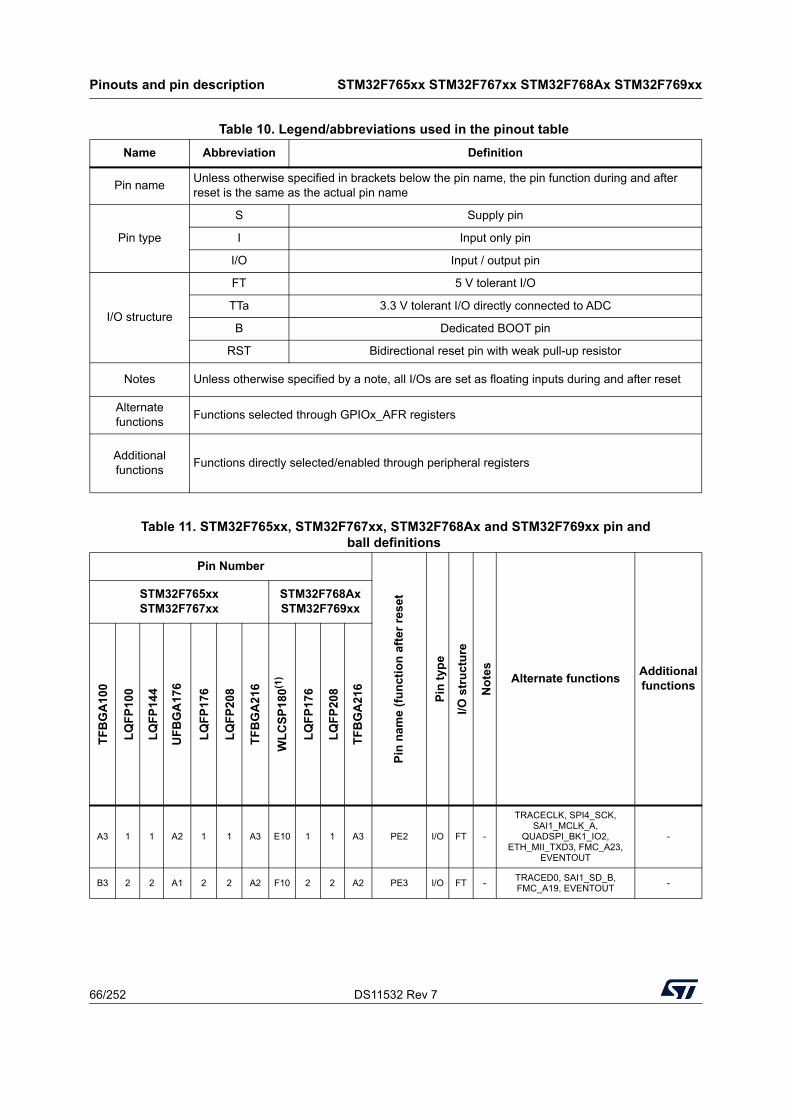
Pinouts and pin description STM32F765xx STM32F767xx STM32F768Ax STM32F769xx
66/252 DS11532 Rev 7
Table 10. Legend/abbreviations used in the pinout table
Name Abbreviation Definition
Pin nameUnless otherwise specified in brackets below the pin name, the pin function during and after reset is the same as the actual pin name
Pin type
S Supply pin
I Input only pin
I/O Input / output pin
I/O structure
FT 5 V tolerant I/O
TTa 3.3 V tolerant I/O directly connected to ADC
B Dedicated BOOT pin
RST Bidirectional reset pin with weak pull-up resistor
Notes Unless otherwise specified by a note, all I/Os are set as floating inputs during and after reset
Alternate functions
Functions selected through GPIOx_AFR registers
Additional functions
Functions directly selected/enabled through peripheral registers
Table 11. STM32F765xx, STM32F767xx, STM32F768Ax and STM32F769xx pin andball definitions
Pin Number
Pin
nam
e (f
un
ctio
n a
fter
res
et
Pin
typ
e
I/O s
tru
ctu
re
No
tes
Alternate functionsAdditional functions
STM32F765xxSTM32F767xx
STM32F768AxSTM32F769xx
TF
BG
A10
0
LQ
FP
100
LQ
FP
144
UF
BG
A17
6
LQ
FP
176
LQ
FP
208
TF
BG
A21
6
WL
CS
P18
0(1)
LQ
FP
176
LQ
FP
208
TF
BG
A21
6
A3 1 1 A2 1 1 A3 E10 1 1 A3 PE2 I/O FT -
TRACECLK, SPI4_SCK, SAI1_MCLK_A,
QUADSPI_BK1_IO2, ETH_MII_TXD3, FMC_A23,
EVENTOUT
-
B3 2 2 A1 2 2 A2 F10 2 2 A2 PE3 I/O FT -TRACED0, SAI1_SD_B, FMC_A19, EVENTOUT
-
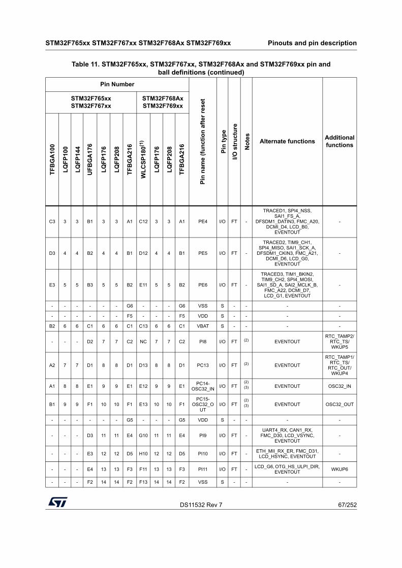
DS11532 Rev 7 67/252
STM32F765xx STM32F767xx STM32F768Ax STM32F769xx Pinouts and pin description
102
C3 3 3 B1 3 3 A1 C12 3 3 A1 PE4 I/O FT -
TRACED1, SPI4_NSS, SAI1_FS_A,
DFSDM1_DATIN3, FMC_A20, DCMI_D4, LCD_B0,
EVENTOUT
-
D3 4 4 B2 4 4 B1 D12 4 4 B1 PE5 I/O FT -
TRACED2, TIM9_CH1, SPI4_MISO, SAI1_SCK_A,
DFSDM1_CKIN3, FMC_A21, DCMI_D6, LCD_G0,
EVENTOUT
-
E3 5 5 B3 5 5 B2 E11 5 5 B2 PE6 I/O FT -
TRACED3, TIM1_BKIN2, TIM9_CH2, SPI4_MOSI,
SAI1_SD_A, SAI2_MCLK_B, FMC_A22, DCMI_D7, LCD_G1, EVENTOUT
-
- - - - - - G6 - - - G6 VSS S - - - -
- - - - - - F5 - - - F5 VDD S - - - -
B2 6 6 C1 6 6 C1 C13 6 6 C1 VBAT S - - - -
- - - D2 7 7 C2 NC 7 7 C2 PI8 I/O FT (2) EVENTOUTRTC_TAMP2/
RTC_TS/WKUP5
A2 7 7 D1 8 8 D1 D13 8 8 D1 PC13 I/O FT (2) EVENTOUT
RTC_TAMP1/RTC_TS/
RTC_OUT/WKUP4
A1 8 8 E1 9 9 E1 E12 9 9 E1PC14-
OSC32_INI/O FT
(2)
(3) EVENTOUT OSC32_IN
B1 9 9 F1 10 10 F1 E13 10 10 F1PC15-
OSC32_OUT
I/O FT(2)
(3) EVENTOUT OSC32_OUT
- - - - - - G5 - - - G5 VDD S - - - -
- - - D3 11 11 E4 G10 11 11 E4 PI9 I/O FT -UART4_RX, CAN1_RX,
FMC_D30, LCD_VSYNC, EVENTOUT
-
- - - E3 12 12 D5 H10 12 12 D5 PI10 I/O FT -ETH_MII_RX_ER, FMC_D31,
LCD_HSYNC, EVENTOUT-
- - - E4 13 13 F3 F11 13 13 F3 PI11 I/O FT -LCD_G6, OTG_HS_ULPI_DIR,
EVENTOUTWKUP6
- - - F2 14 14 F2 F13 14 14 F2 VSS S - - - -
Table 11. STM32F765xx, STM32F767xx, STM32F768Ax and STM32F769xx pin andball definitions (continued)
Pin Number
Pin
nam
e (f
un
ctio
n a
fte
r re
set
Pin
typ
e
I/O s
tru
ctu
re
No
tes
Alternate functionsAdditional functions
STM32F765xxSTM32F767xx
STM32F768AxSTM32F769xx
TF
BG
A10
0
LQ
FP
100
LQ
FP
144
UF
BG
A1
76
LQ
FP
176
LQ
FP
208
TF
BG
A21
6
WL
CS
P18
0(1)
LQ
FP
176
LQ
FP
208
TF
BG
A21
6
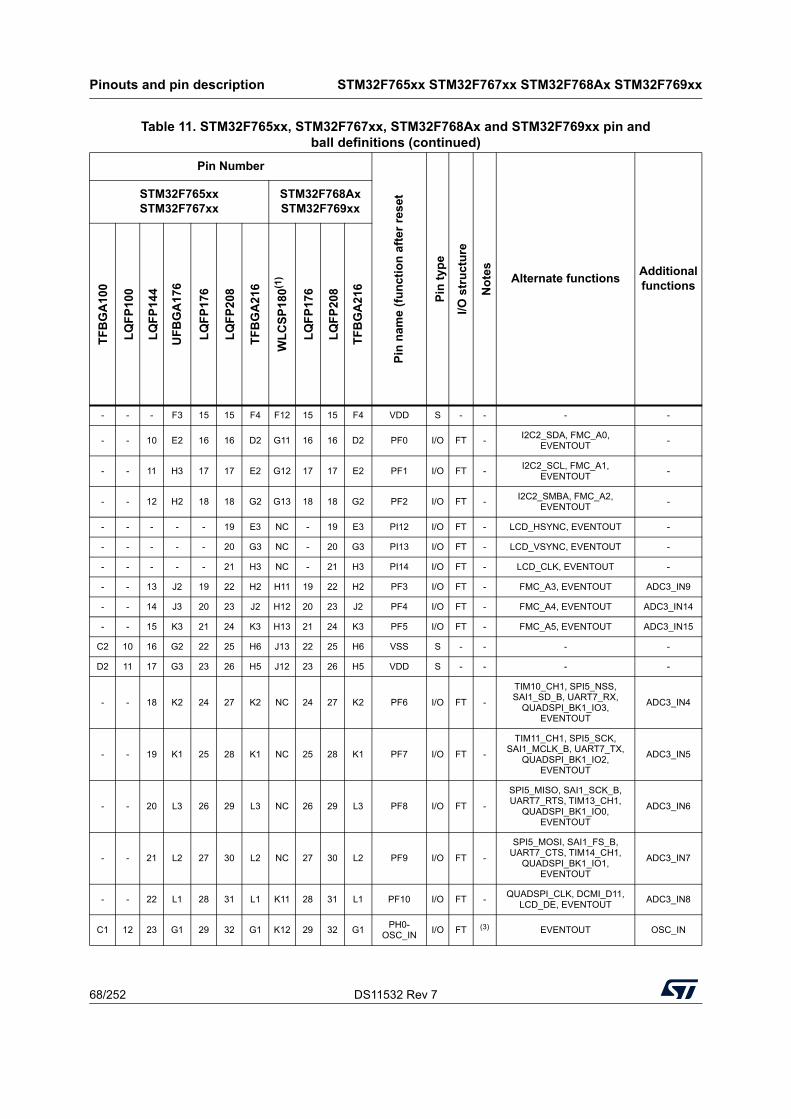
Pinouts and pin description STM32F765xx STM32F767xx STM32F768Ax STM32F769xx
68/252 DS11532 Rev 7
- - - F3 15 15 F4 F12 15 15 F4 VDD S - - - -
- - 10 E2 16 16 D2 G11 16 16 D2 PF0 I/O FT -I2C2_SDA, FMC_A0,
EVENTOUT-
- - 11 H3 17 17 E2 G12 17 17 E2 PF1 I/O FT -I2C2_SCL, FMC_A1,
EVENTOUT-
- - 12 H2 18 18 G2 G13 18 18 G2 PF2 I/O FT -I2C2_SMBA, FMC_A2,
EVENTOUT-
- - - - - 19 E3 NC - 19 E3 PI12 I/O FT - LCD_HSYNC, EVENTOUT -
- - - - - 20 G3 NC - 20 G3 PI13 I/O FT - LCD_VSYNC, EVENTOUT -
- - - - - 21 H3 NC - 21 H3 PI14 I/O FT - LCD_CLK, EVENTOUT -
- - 13 J2 19 22 H2 H11 19 22 H2 PF3 I/O FT - FMC_A3, EVENTOUT ADC3_IN9
- - 14 J3 20 23 J2 H12 20 23 J2 PF4 I/O FT - FMC_A4, EVENTOUT ADC3_IN14
- - 15 K3 21 24 K3 H13 21 24 K3 PF5 I/O FT - FMC_A5, EVENTOUT ADC3_IN15
C2 10 16 G2 22 25 H6 J13 22 25 H6 VSS S - - - -
D2 11 17 G3 23 26 H5 J12 23 26 H5 VDD S - - - -
- - 18 K2 24 27 K2 NC 24 27 K2 PF6 I/O FT -
TIM10_CH1, SPI5_NSS, SAI1_SD_B, UART7_RX,
QUADSPI_BK1_IO3, EVENTOUT
ADC3_IN4
- - 19 K1 25 28 K1 NC 25 28 K1 PF7 I/O FT -
TIM11_CH1, SPI5_SCK, SAI1_MCLK_B, UART7_TX,
QUADSPI_BK1_IO2, EVENTOUT
ADC3_IN5
- - 20 L3 26 29 L3 NC 26 29 L3 PF8 I/O FT -
SPI5_MISO, SAI1_SCK_B, UART7_RTS, TIM13_CH1,
QUADSPI_BK1_IO0, EVENTOUT
ADC3_IN6
- - 21 L2 27 30 L2 NC 27 30 L2 PF9 I/O FT -
SPI5_MOSI, SAI1_FS_B, UART7_CTS, TIM14_CH1,
QUADSPI_BK1_IO1, EVENTOUT
ADC3_IN7
- - 22 L1 28 31 L1 K11 28 31 L1 PF10 I/O FT -QUADSPI_CLK, DCMI_D11,
LCD_DE, EVENTOUTADC3_IN8
C1 12 23 G1 29 32 G1 K12 29 32 G1PH0-
OSC_INI/O FT (3) EVENTOUT OSC_IN
Table 11. STM32F765xx, STM32F767xx, STM32F768Ax and STM32F769xx pin andball definitions (continued)
Pin Number
Pin
nam
e (f
un
ctio
n a
fte
r re
set
Pin
typ
e
I/O s
tru
ctu
re
No
tes
Alternate functionsAdditional functions
STM32F765xxSTM32F767xx
STM32F768AxSTM32F769xx
TF
BG
A10
0
LQ
FP
100
LQ
FP
144
UF
BG
A1
76
LQ
FP
176
LQ
FP
208
TF
BG
A21
6
WL
CS
P18
0(1)
LQ
FP
176
LQ
FP
208
TF
BG
A21
6
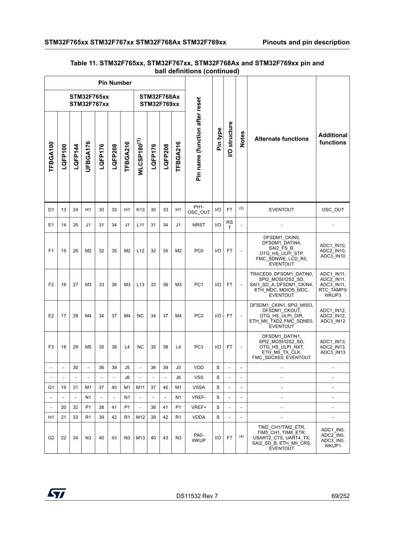
DS11532 Rev 7 69/252
STM32F765xx STM32F767xx STM32F768Ax STM32F769xx Pinouts and pin description
102
D1 13 24 H1 30 33 H1 K13 30 33 H1PH1-
OSC_OUTI/O FT (3) EVENTOUT OSC_OUT
E1 14 25 J1 31 34 J1 L11 31 34 J1 NRST I/ORST
- - -
F1 15 26 M2 32 35 M2 L12 32 35 M2 PC0 I/O FT -
DFSDM1_CKIN0, DFSDM1_DATIN4,
SAI2_FS_B, OTG_HS_ULPI_STP,
FMC_SDNWE, LCD_R5, EVENTOUT
ADC1_IN10, ADC2_IN10, ADC3_IN10
F2 16 27 M3 33 36 M3 L13 33 36 M3 PC1 I/O FT -
TRACED0, DFSDM1_DATIN0, SPI2_MOSI/I2S2_SD,
SAI1_SD_A, DFSDM1_CKIN4, ETH_MDC, MDIOS_MDC,
EVENTOUT
ADC1_IN11, ADC2_IN11, ADC3_IN11,
RTC_TAMP3/WKUP3
E2 17 28 M4 34 37 M4 NC 34 37 M4 PC2 I/O FT -
DFSDM1_CKIN1, SPI2_MISO, DFSDM1_CKOUT,
OTG_HS_ULPI_DIR, ETH_MII_TXD2, FMC_SDNE0,
EVENTOUT
ADC1_IN12, ADC2_IN12, ADC3_IN12
F3 18 29 M5 35 38 L4 NC 35 38 L4 PC3 I/O FT -
DFSDM1_DATIN1, SPI2_MOSI/I2S2_SD, OTG_HS_ULPI_NXT, ETH_MII_TX_CLK,
FMC_SDCKE0, EVENTOUT
ADC1_IN13, ADC2_IN13, ADC3_IN13
- - 30 - 36 39 J5 - 36 39 J5 VDD S - - - -
- - - - - - J6 - - - J6 VSS S - - - -
G1 19 31 M1 37 40 M1 M11 37 40 M1 VSSA S - - - -
- - - N1 - - N1 - - - N1 VREF- S - - - -
- 20 32 P1 38 41 P1 - 38 41 P1 VREF+ S - - - -
H1 21 33 R1 39 42 R1 M12 39 42 R1 VDDA S - - - -
G2 22 34 N3 40 43 N3 M13 40 43 N3PA0-
WKUPI/O FT (4)
TIM2_CH1/TIM2_ETR, TIM5_CH1, TIM8_ETR,
USART2_CTS, UART4_TX, SAI2_SD_B, ETH_MII_CRS,
EVENTOUT
ADC1_IN0, ADC2_IN0, ADC3_IN0,
WKUP1
Table 11. STM32F765xx, STM32F767xx, STM32F768Ax and STM32F769xx pin andball definitions (continued)
Pin Number
Pin
nam
e (f
un
ctio
n a
fte
r re
set
Pin
typ
e
I/O s
tru
ctu
re
No
tes
Alternate functionsAdditional functions
STM32F765xxSTM32F767xx
STM32F768AxSTM32F769xx
TF
BG
A10
0
LQ
FP
100
LQ
FP
144
UF
BG
A1
76
LQ
FP
176
LQ
FP
208
TF
BG
A21
6
WL
CS
P18
0(1)
LQ
FP
176
LQ
FP
208
TF
BG
A21
6
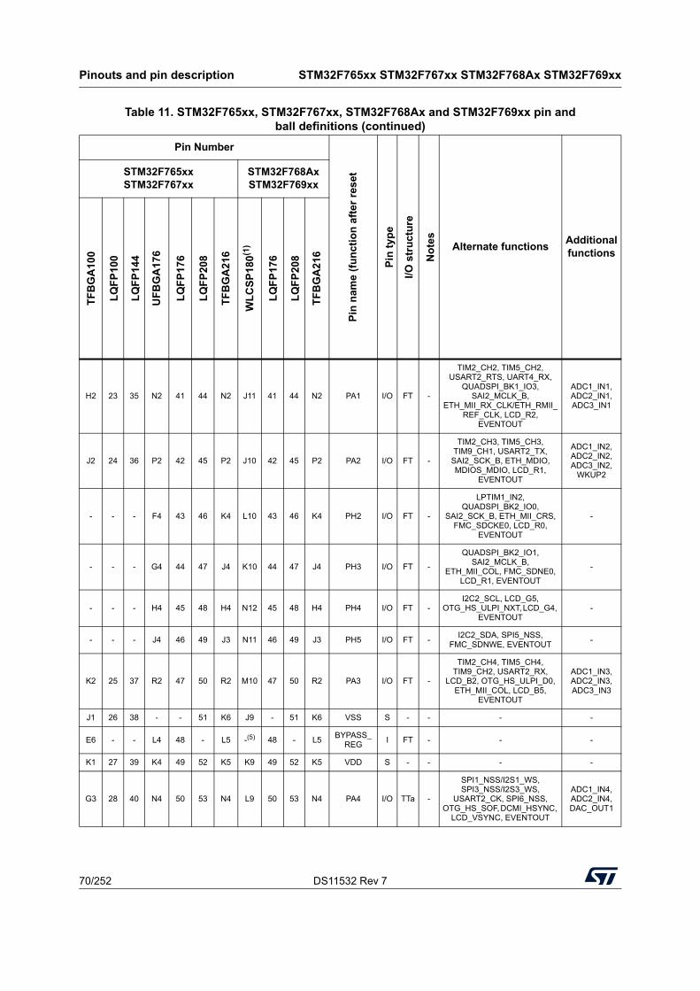
Pinouts and pin description STM32F765xx STM32F767xx STM32F768Ax STM32F769xx
70/252 DS11532 Rev 7
H2 23 35 N2 41 44 N2 J11 41 44 N2 PA1 I/O FT -
TIM2_CH2, TIM5_CH2, USART2_RTS, UART4_RX,
QUADSPI_BK1_IO3, SAI2_MCLK_B,
ETH_MII_RX_CLK/ETH_RMII_REF_CLK, LCD_R2,
EVENTOUT
ADC1_IN1, ADC2_IN1, ADC3_IN1
J2 24 36 P2 42 45 P2 J10 42 45 P2 PA2 I/O FT -
TIM2_CH3, TIM5_CH3, TIM9_CH1, USART2_TX,
SAI2_SCK_B, ETH_MDIO, MDIOS_MDIO, LCD_R1,
EVENTOUT
ADC1_IN2, ADC2_IN2, ADC3_IN2,
WKUP2
- - - F4 43 46 K4 L10 43 46 K4 PH2 I/O FT -
LPTIM1_IN2, QUADSPI_BK2_IO0,
SAI2_SCK_B, ETH_MII_CRS, FMC_SDCKE0, LCD_R0,
EVENTOUT
-
- - - G4 44 47 J4 K10 44 47 J4 PH3 I/O FT -
QUADSPI_BK2_IO1, SAI2_MCLK_B,
ETH_MII_COL, FMC_SDNE0, LCD_R1, EVENTOUT
-
- - - H4 45 48 H4 N12 45 48 H4 PH4 I/O FT -I2C2_SCL, LCD_G5,
OTG_HS_ULPI_NXT, LCD_G4, EVENTOUT
-
- - - J4 46 49 J3 N11 46 49 J3 PH5 I/O FT -I2C2_SDA, SPI5_NSS,
FMC_SDNWE, EVENTOUT-
K2 25 37 R2 47 50 R2 M10 47 50 R2 PA3 I/O FT -
TIM2_CH4, TIM5_CH4, TIM9_CH2, USART2_RX,
LCD_B2, OTG_HS_ULPI_D0, ETH_MII_COL, LCD_B5,
EVENTOUT
ADC1_IN3, ADC2_IN3, ADC3_IN3
J1 26 38 - - 51 K6 J9 - 51 K6 VSS S - - - -
E6 - - L4 48 - L5 -(5) 48 - L5BYPASS_
REGI FT - - -
K1 27 39 K4 49 52 K5 K9 49 52 K5 VDD S - - - -
G3 28 40 N4 50 53 N4 L9 50 53 N4 PA4 I/O TTa -
SPI1_NSS/I2S1_WS, SPI3_NSS/I2S3_WS,
USART2_CK, SPI6_NSS, OTG_HS_SOF, DCMI_HSYNC,
LCD_VSYNC, EVENTOUT
ADC1_IN4, ADC2_IN4, DAC_OUT1
Table 11. STM32F765xx, STM32F767xx, STM32F768Ax and STM32F769xx pin andball definitions (continued)
Pin Number
Pin
nam
e (f
un
ctio
n a
fte
r re
set
Pin
typ
e
I/O s
tru
ctu
re
No
tes
Alternate functionsAdditional functions
STM32F765xxSTM32F767xx
STM32F768AxSTM32F769xx
TF
BG
A10
0
LQ
FP
100
LQ
FP
144
UF
BG
A1
76
LQ
FP
176
LQ
FP
208
TF
BG
A21
6
WL
CS
P18
0(1)
LQ
FP
176
LQ
FP
208
TF
BG
A21
6
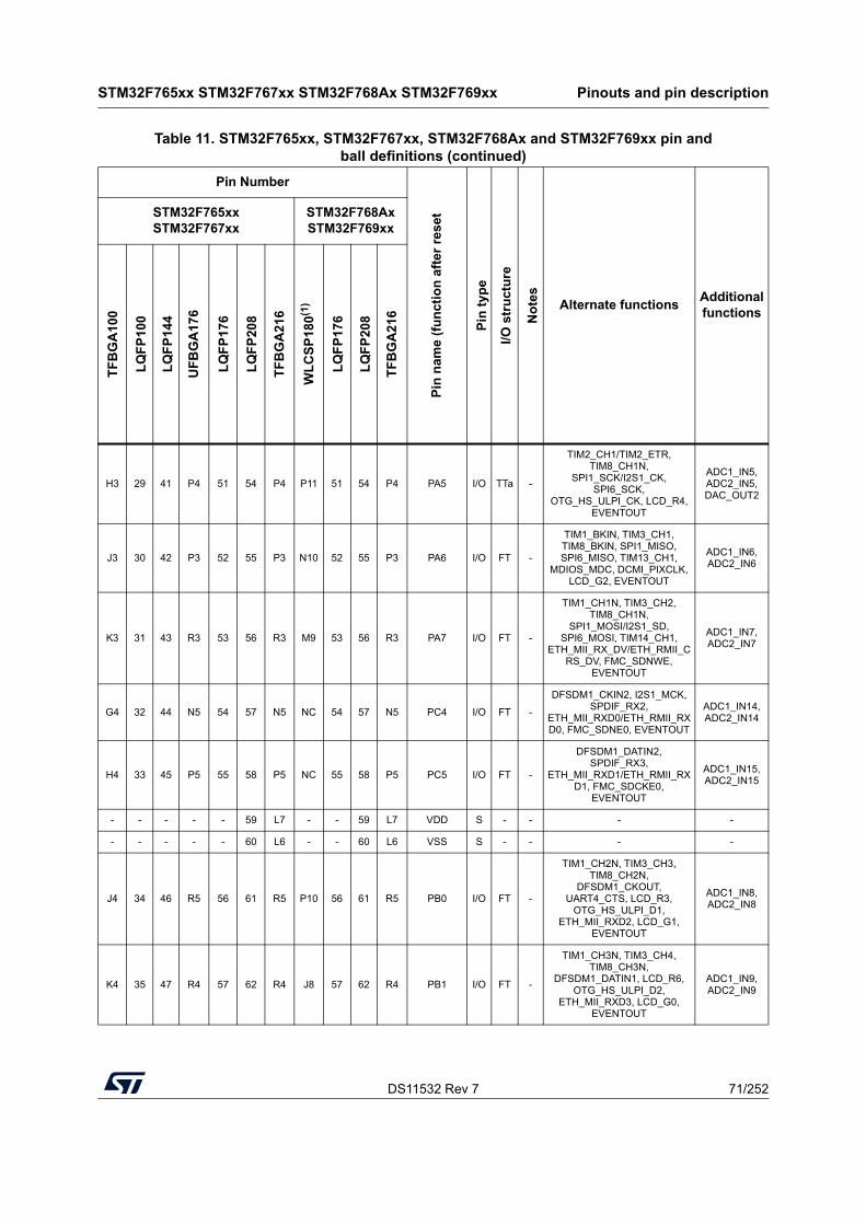
DS11532 Rev 7 71/252
STM32F765xx STM32F767xx STM32F768Ax STM32F769xx Pinouts and pin description
102
H3 29 41 P4 51 54 P4 P11 51 54 P4 PA5 I/O TTa -
TIM2_CH1/TIM2_ETR, TIM8_CH1N,
SPI1_SCK/I2S1_CK, SPI6_SCK,
OTG_HS_ULPI_CK, LCD_R4, EVENTOUT
ADC1_IN5, ADC2_IN5, DAC_OUT2
J3 30 42 P3 52 55 P3 N10 52 55 P3 PA6 I/O FT -
TIM1_BKIN, TIM3_CH1, TIM8_BKIN, SPI1_MISO, SPI6_MISO, TIM13_CH1,
MDIOS_MDC, DCMI_PIXCLK, LCD_G2, EVENTOUT
ADC1_IN6, ADC2_IN6
K3 31 43 R3 53 56 R3 M9 53 56 R3 PA7 I/O FT -
TIM1_CH1N, TIM3_CH2, TIM8_CH1N,
SPI1_MOSI/I2S1_SD, SPI6_MOSI, TIM14_CH1,
ETH_MII_RX_DV/ETH_RMII_CRS_DV, FMC_SDNWE,
EVENTOUT
ADC1_IN7, ADC2_IN7
G4 32 44 N5 54 57 N5 NC 54 57 N5 PC4 I/O FT -
DFSDM1_CKIN2, I2S1_MCK, SPDIF_RX2,
ETH_MII_RXD0/ETH_RMII_RXD0, FMC_SDNE0, EVENTOUT
ADC1_IN14, ADC2_IN14
H4 33 45 P5 55 58 P5 NC 55 58 P5 PC5 I/O FT -
DFSDM1_DATIN2, SPDIF_RX3,
ETH_MII_RXD1/ETH_RMII_RXD1, FMC_SDCKE0,
EVENTOUT
ADC1_IN15, ADC2_IN15
- - - - - 59 L7 - - 59 L7 VDD S - - - -
- - - - - 60 L6 - - 60 L6 VSS S - - - -
J4 34 46 R5 56 61 R5 P10 56 61 R5 PB0 I/O FT -
TIM1_CH2N, TIM3_CH3, TIM8_CH2N,
DFSDM1_CKOUT, UART4_CTS, LCD_R3,
OTG_HS_ULPI_D1, ETH_MII_RXD2, LCD_G1,
EVENTOUT
ADC1_IN8, ADC2_IN8
K4 35 47 R4 57 62 R4 J8 57 62 R4 PB1 I/O FT -
TIM1_CH3N, TIM3_CH4, TIM8_CH3N,
DFSDM1_DATIN1, LCD_R6, OTG_HS_ULPI_D2,
ETH_MII_RXD3, LCD_G0, EVENTOUT
ADC1_IN9, ADC2_IN9
Table 11. STM32F765xx, STM32F767xx, STM32F768Ax and STM32F769xx pin andball definitions (continued)
Pin Number
Pin
nam
e (f
un
ctio
n a
fte
r re
set
Pin
typ
e
I/O s
tru
ctu
re
No
tes
Alternate functionsAdditional functions
STM32F765xxSTM32F767xx
STM32F768AxSTM32F769xx
TF
BG
A10
0
LQ
FP
100
LQ
FP
144
UF
BG
A1
76
LQ
FP
176
LQ
FP
208
TF
BG
A21
6
WL
CS
P18
0(1)
LQ
FP
176
LQ
FP
208
TF
BG
A21
6
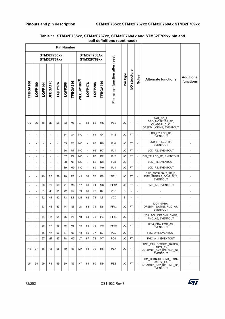
Pinouts and pin description STM32F765xx STM32F767xx STM32F768Ax STM32F769xx
72/252 DS11532 Rev 7
G5 36 48 M6 58 63 M5 J7 58 63 M5 PB2 I/O FT -
SAI1_SD_A, SPI3_MOSI/I2S3_SD,
QUADSPI_CLK, DFSDM1_CKIN1, EVENTOUT
-
- - - - - 64 G4 NC - 64 G4 PI15 I/O FT -LCD_G2, LCD_R0,
EVENTOUT-
- - - - - 65 R6 NC - 65 R6 PJ0 I/O FT -LCD_R7, LCD_R1,
EVENTOUT-
- - - - - 66 R7 NC - 66 R7 PJ1 I/O FT - LCD_R2, EVENTOUT -
- - - - - 67 P7 NC - 67 P7 PJ2 I/O FT - DSI_TE, LCD_R3, EVENTOUT -
- - - - - 68 N8 NC - 68 N8 PJ3 I/O FT - LCD_R4, EVENTOUT -
- - - - - 69 M9 NC - 69 M9 PJ4 I/O FT - LCD_R5, EVENTOUT -
- - 49 R6 59 70 P8 N9 59 70 P8 PF11 I/O FT -SPI5_MOSI, SAI2_SD_B,
FMC_SDNRAS, DCMI_D12, EVENTOUT
-
- - 50 P6 60 71 M6 K7 60 71 M6 PF12 I/O FT - FMC_A6, EVENTOUT -
- - 51 M8 61 72 K7 P9 61 72 K7 VSS S - - - -
- - 52 N8 62 73 L8 M8 62 73 L8 VDD S - - - -
- - 53 N6 63 74 N6 L8 63 74 N6 PF13 I/O FT -I2C4_SMBA,
DFSDM1_DATIN6, FMC_A7, EVENTOUT
-
- - 54 R7 64 75 P6 K8 64 75 P6 PF14 I/O FT -I2C4_SCL, DFSDM1_CKIN6,
FMC_A8, EVENTOUT-
- - 55 P7 65 76 M8 P8 65 76 M8 PF15 I/O FT -I2C4_SDA, FMC_A9,
EVENTOUT-
- - 56 N7 66 77 N7 N8 66 77 N7 PG0 I/O FT - FMC_A10, EVENTOUT -
- - 57 M7 67 78 M7 L7 67 78 M7 PG1 I/O FT - FMC_A11, EVENTOUT -
H5 37 58 R8 68 79 R8 M7 68 79 R8 PE7 I/O FT -
TIM1_ETR, DFSDM1_DATIN2, UART7_RX,
QUADSPI_BK2_IO0, FMC_D4, EVENTOUT
-
J5 38 59 P8 69 80 N9 N7 69 80 N9 PE8 I/O FT -
TIM1_CH1N, DFSDM1_CKIN2, UART7_TX,
QUADSPI_BK2_IO1, FMC_D5, EVENTOUT
-
Table 11. STM32F765xx, STM32F767xx, STM32F768Ax and STM32F769xx pin andball definitions (continued)
Pin Number
Pin
nam
e (f
un
ctio
n a
fte
r re
set
Pin
typ
e
I/O s
tru
ctu
re
No
tes
Alternate functionsAdditional functions
STM32F765xxSTM32F767xx
STM32F768AxSTM32F769xx
TF
BG
A10
0
LQ
FP
100
LQ
FP
144
UF
BG
A1
76
LQ
FP
176
LQ
FP
208
TF
BG
A21
6
WL
CS
P18
0(1)
LQ
FP
176
LQ
FP
208
TF
BG
A21
6
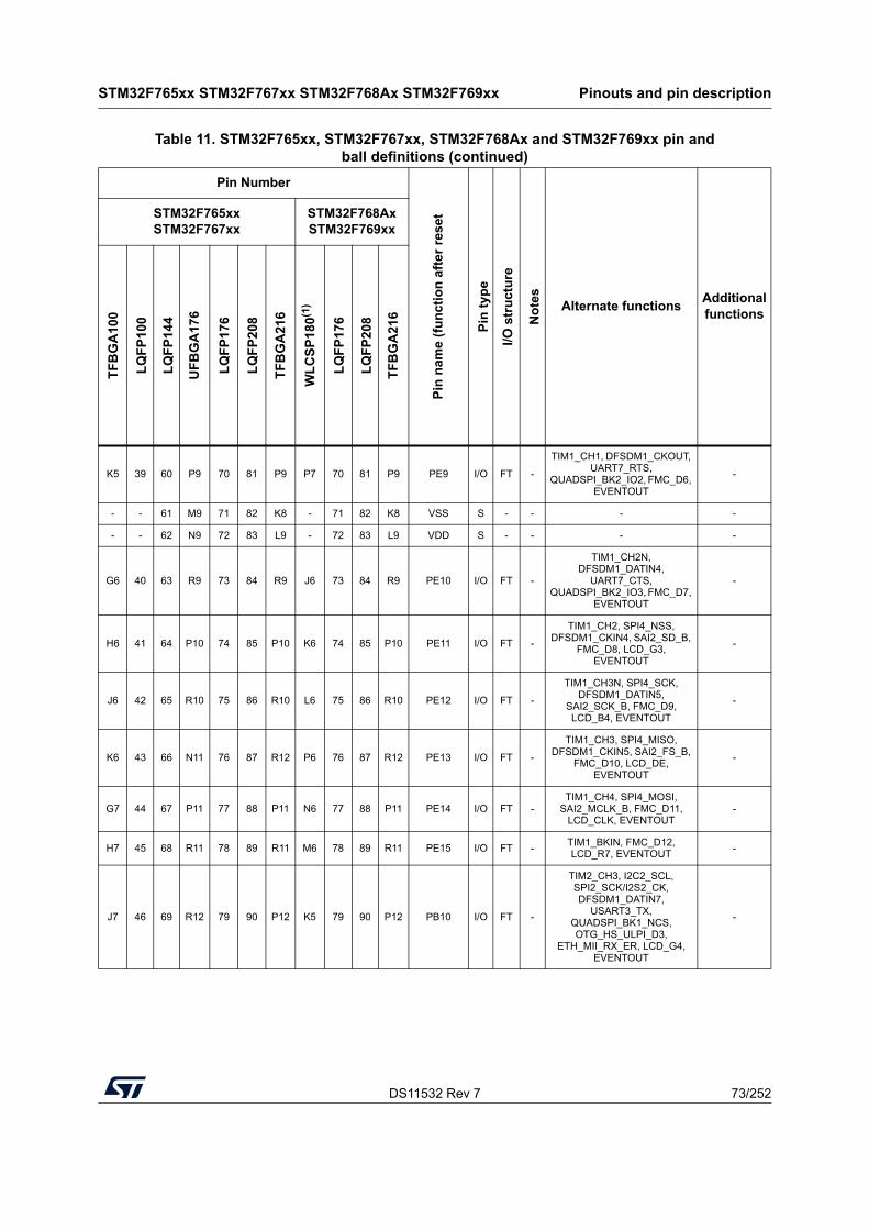
DS11532 Rev 7 73/252
STM32F765xx STM32F767xx STM32F768Ax STM32F769xx Pinouts and pin description
102
K5 39 60 P9 70 81 P9 P7 70 81 P9 PE9 I/O FT -
TIM1_CH1, DFSDM1_CKOUT, UART7_RTS,
QUADSPI_BK2_IO2, FMC_D6, EVENTOUT
-
- - 61 M9 71 82 K8 - 71 82 K8 VSS S - - - -
- - 62 N9 72 83 L9 - 72 83 L9 VDD S - - - -
G6 40 63 R9 73 84 R9 J6 73 84 R9 PE10 I/O FT -
TIM1_CH2N, DFSDM1_DATIN4,
UART7_CTS, QUADSPI_BK2_IO3, FMC_D7,
EVENTOUT
-
H6 41 64 P10 74 85 P10 K6 74 85 P10 PE11 I/O FT -
TIM1_CH2, SPI4_NSS, DFSDM1_CKIN4, SAI2_SD_B,
FMC_D8, LCD_G3, EVENTOUT
-
J6 42 65 R10 75 86 R10 L6 75 86 R10 PE12 I/O FT -
TIM1_CH3N, SPI4_SCK, DFSDM1_DATIN5,
SAI2_SCK_B, FMC_D9, LCD_B4, EVENTOUT
-
K6 43 66 N11 76 87 R12 P6 76 87 R12 PE13 I/O FT -
TIM1_CH3, SPI4_MISO, DFSDM1_CKIN5, SAI2_FS_B,
FMC_D10, LCD_DE, EVENTOUT
-
G7 44 67 P11 77 88 P11 N6 77 88 P11 PE14 I/O FT -TIM1_CH4, SPI4_MOSI,
SAI2_MCLK_B, FMC_D11, LCD_CLK, EVENTOUT
-
H7 45 68 R11 78 89 R11 M6 78 89 R11 PE15 I/O FT -TIM1_BKIN, FMC_D12, LCD_R7, EVENTOUT
-
J7 46 69 R12 79 90 P12 K5 79 90 P12 PB10 I/O FT -
TIM2_CH3, I2C2_SCL, SPI2_SCK/I2S2_CK, DFSDM1_DATIN7,
USART3_TX, QUADSPI_BK1_NCS, OTG_HS_ULPI_D3,
ETH_MII_RX_ER, LCD_G4, EVENTOUT
-
Table 11. STM32F765xx, STM32F767xx, STM32F768Ax and STM32F769xx pin andball definitions (continued)
Pin Number
Pin
nam
e (f
un
ctio
n a
fte
r re
set
Pin
typ
e
I/O s
tru
ctu
re
No
tes
Alternate functionsAdditional functions
STM32F765xxSTM32F767xx
STM32F768AxSTM32F769xx
TF
BG
A10
0
LQ
FP
100
LQ
FP
144
UF
BG
A1
76
LQ
FP
176
LQ
FP
208
TF
BG
A21
6
WL
CS
P18
0(1)
LQ
FP
176
LQ
FP
208
TF
BG
A21
6
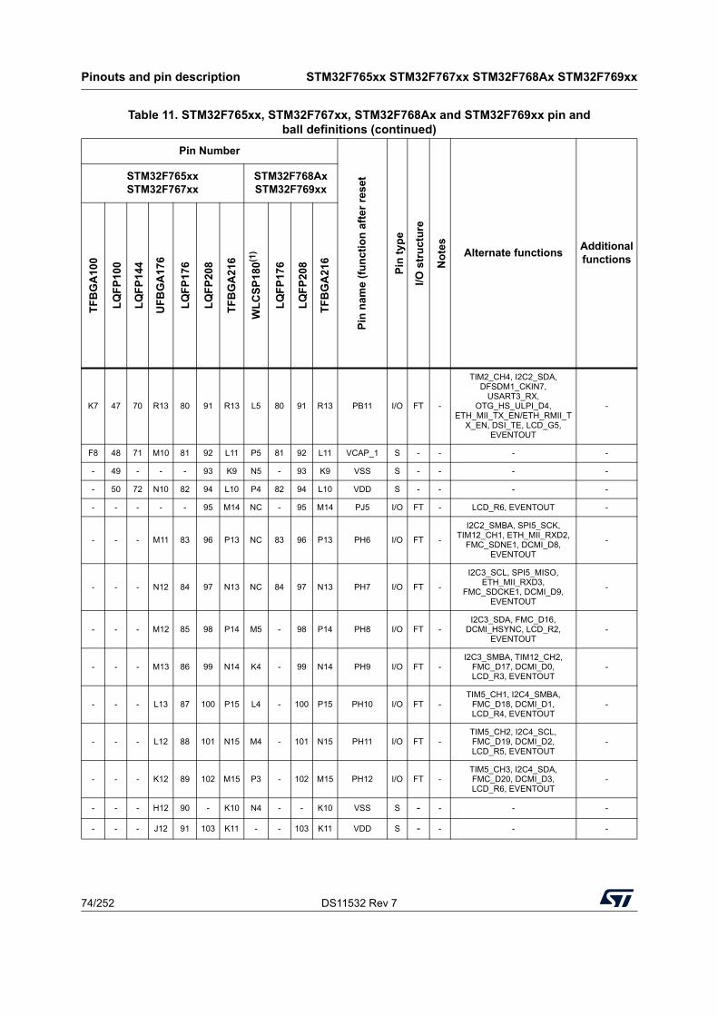
Pinouts and pin description STM32F765xx STM32F767xx STM32F768Ax STM32F769xx
74/252 DS11532 Rev 7
K7 47 70 R13 80 91 R13 L5 80 91 R13 PB11 I/O FT -
TIM2_CH4, I2C2_SDA, DFSDM1_CKIN7,
USART3_RX, OTG_HS_ULPI_D4,
ETH_MII_TX_EN/ETH_RMII_TX_EN, DSI_TE, LCD_G5,
EVENTOUT
-
F8 48 71 M10 81 92 L11 P5 81 92 L11 VCAP_1 S - - - -
- 49 - - - 93 K9 N5 - 93 K9 VSS S - - - -
- 50 72 N10 82 94 L10 P4 82 94 L10 VDD S - - - -
- - - - - 95 M14 NC - 95 M14 PJ5 I/O FT - LCD_R6, EVENTOUT -
- - - M11 83 96 P13 NC 83 96 P13 PH6 I/O FT -
I2C2_SMBA, SPI5_SCK, TIM12_CH1, ETH_MII_RXD2,
FMC_SDNE1, DCMI_D8, EVENTOUT
-
- - - N12 84 97 N13 NC 84 97 N13 PH7 I/O FT -
I2C3_SCL, SPI5_MISO, ETH_MII_RXD3,
FMC_SDCKE1, DCMI_D9, EVENTOUT
-
- - - M12 85 98 P14 M5 - 98 P14 PH8 I/O FT -I2C3_SDA, FMC_D16,
DCMI_HSYNC, LCD_R2, EVENTOUT
-
- - - M13 86 99 N14 K4 - 99 N14 PH9 I/O FT -I2C3_SMBA, TIM12_CH2,
FMC_D17, DCMI_D0, LCD_R3, EVENTOUT
-
- - - L13 87 100 P15 L4 - 100 P15 PH10 I/O FT -TIM5_CH1, I2C4_SMBA,
FMC_D18, DCMI_D1, LCD_R4, EVENTOUT
-
- - - L12 88 101 N15 M4 - 101 N15 PH11 I/O FT -TIM5_CH2, I2C4_SCL, FMC_D19, DCMI_D2, LCD_R5, EVENTOUT
-
- - - K12 89 102 M15 P3 - 102 M15 PH12 I/O FT -TIM5_CH3, I2C4_SDA, FMC_D20, DCMI_D3, LCD_R6, EVENTOUT
-
- - - H12 90 - K10 N4 - - K10 VSS S - - - -
- - - J12 91 103 K11 - - 103 K11 VDD S - - - -
Table 11. STM32F765xx, STM32F767xx, STM32F768Ax and STM32F769xx pin andball definitions (continued)
Pin Number
Pin
nam
e (f
un
ctio
n a
fte
r re
set
Pin
typ
e
I/O s
tru
ctu
re
No
tes
Alternate functionsAdditional functions
STM32F765xxSTM32F767xx
STM32F768AxSTM32F769xx
TF
BG
A10
0
LQ
FP
100
LQ
FP
144
UF
BG
A1
76
LQ
FP
176
LQ
FP
208
TF
BG
A21
6
WL
CS
P18
0(1)
LQ
FP
176
LQ
FP
208
TF
BG
A21
6
DS11532 Rev 7 75/252
STM32F765xx STM32F767xx STM32F768Ax STM32F769xx Pinouts and pin description
102
K8 51 73 P12 92 104 L13 H8 85 104 L13 PB12 I/O FT -
TIM1_BKIN, I2C2_SMBA, SPI2_NSS/I2S2_WS,
DFSDM1_DATIN1, USART3_CK, UART5_RX,
CAN2_RX, OTG_HS_ULPI_D5,
ETH_MII_TXD0/ETH_RMII_TXD0, OTG_HS_ID, EVENTOUT
-
J8 52 74 P13 93 105 K14 J5 86 105 K14 PB13 I/O FT -
TIM1_CH1N, SPI2_SCK/I2S2_CK,
DFSDM1_CKIN1, USART3_CTS, UART5_TX,
CAN2_TX, OTG_HS_ULPI_D6, ETH_MII_TXD1/ETH_RMII_TX
D1, EVENTOUT
OTG_HS_VBUS
H10 53 75 R14 94 106 R14 N3 87 106 R14 PB14 I/O FT -
TIM1_CH2N, TIM8_CH2N, USART1_TX, SPI2_MISO,
DFSDM1_DATIN2, USART3_RTS, UART4_RTS, TIM12_CH1, SDMMC2_D0, OTG_HS_DM, EVENTOUT
-
G10 54 76 R15 95 107 R15 N2 88 107 R15 PB15 I/O FT -
RTC_REFIN, TIM1_CH3N, TIM8_CH3N, USART1_RX,
SPI2_MOSI/I2S2_SD, DFSDM1_CKIN2,
UART4_CTS, TIM12_CH2, SDMMC2_D1, OTG_HS_DP,
EVENTOUT
-
K9 55 77 P15 96 108 L15 M3 89 108 L15 PD8 I/O FT -DFSDM1_CKIN3,
USART3_TX, SPDIF_RX1, FMC_D13, EVENTOUT
-
J9 56 78 P14 97 109 L14 L3 90 109 L14 PD9 I/O FT -DFSDM1_DATIN3,
USART3_RX, FMC_D14, EVENTOUT
-
H9 57 79 N15 98 110 K15 M2 91 110 K15 PD10 I/O FT -DFSDM1_CKOUT,
USART3_CK, FMC_D15, LCD_B3, EVENTOUT
-
G9 58 80 N14 99 111 N10 K3 92 111 N10 PD11 I/O FT -
I2C4_SMBA, USART3_CTS, QUADSPI_BK1_IO0,
SAI2_SD_A, FMC_A16/FMC_CLE,
EVENTOUT
-
Table 11. STM32F765xx, STM32F767xx, STM32F768Ax and STM32F769xx pin andball definitions (continued)
Pin Number
Pin
nam
e (f
un
ctio
n a
fte
r re
set
Pin
typ
e
I/O s
tru
ctu
re
No
tes
Alternate functionsAdditional functions
STM32F765xxSTM32F767xx
STM32F768AxSTM32F769xx
TF
BG
A10
0
LQ
FP
100
LQ
FP
144
UF
BG
A1
76
LQ
FP
176
LQ
FP
208
TF
BG
A21
6
WL
CS
P18
0(1)
LQ
FP
176
LQ
FP
208
TF
BG
A21
6
Pinouts and pin description STM32F765xx STM32F767xx STM32F768Ax STM32F769xx
76/252 DS11532 Rev 7
K10 59 81 N13 100 112 M10 J4 93 112 M10 PD12 I/O FT -
TIM4_CH1, LPTIM1_IN1, I2C4_SCL, USART3_RTS,
QUADSPI_BK1_IO1, SAI2_FS_A,
FMC_A17/FMC_ALE, EVENTOUT
-
J10 60 82 M15 101 113 M11 L2 94 113 M11 PD13 I/O FT -
TIM4_CH2, LPTIM1_OUT, I2C4_SDA,
QUADSPI_BK1_IO3, SAI2_SCK_A, FMC_A18,
EVENTOUT
-
- - 83 - 102 114 J10 M1 95 114 J10 VSS S - - - -
- - 84 J13 103 115 J11 - 96 115 J11 VDD S - - - -
H8 61 85 M14 104 116 L12 L1 97 116 L12 PD14 I/O FT -TIM4_CH3, UART8_CTS,
FMC_D0, EVENTOUT-
G8 62 86 L14 105 117 K13 K2 98 117 K13 PD15 I/O FT -TIM4_CH4, UART8_RTS,
FMC_D1, EVENTOUT-
- - - - - 118 K12 - - - - PJ6 I/O FT - LCD_R7, EVENTOUT -
- - - - - 119 J12 - - - - PJ7 I/O FT - LCD_G0, EVENTOUT -
- - - - - 120 H12 - - - - PJ8 I/O FT - LCD_G1, EVENTOUT -
- - - - - 121 J13 - - - - PJ9 I/O FT - LCD_G2, EVENTOUT -
- - - - - 122 H13 - - - - PJ10 I/O FT - LCD_G3, EVENTOUT -
- - - - - 123 G12 - - - - PJ11 I/O FT - LCD_G4, EVENTOUT -
- - - - - 124 H11 - - - - VDD S - - - -
- - - - - - - K1 99 118 H11 VDDDSI S - - - -
- - - - - 125 H10 - - - H10 VSS S - - - -
- - - - - - - H6 100 119 K12 VCAPDSI S - - - -
- - - - - - - J3 - - G13 VDD12DSI S - - - -
- - - - - - - J1 101 120 J12 DSI_D0P I/O - - - -
- - - - - - - J2 102 121 J13 DSI_D0N I/O - - - -
- - - - - - - H5 103 122 G12 VSSDSI S - - - -
- - - - - - - H4 104 123 H12 DSI_CKP I/O - - - -
Table 11. STM32F765xx, STM32F767xx, STM32F768Ax and STM32F769xx pin andball definitions (continued)
Pin Number
Pin
nam
e (f
un
ctio
n a
fte
r re
set
Pin
typ
e
I/O s
tru
ctu
re
No
tes
Alternate functionsAdditional functions
STM32F765xxSTM32F767xx
STM32F768AxSTM32F769xx
TF
BG
A10
0
LQ
FP
100
LQ
FP
144
UF
BG
A1
76
LQ
FP
176
LQ
FP
208
TF
BG
A21
6
WL
CS
P18
0(1)
LQ
FP
176
LQ
FP
208
TF
BG
A21
6
DS11532 Rev 7 77/252
STM32F765xx STM32F767xx STM32F768Ax STM32F769xx Pinouts and pin description
102
- - - - - - - H3 105 124 H13 DSI_CKN I/O - - - -
- - - - - - - - 106 125 - VDD12DSI S - - - -
- - - - - - - H1 107 126 F12 DSI_D1P I/O - - - -
- - - - - - - H2 108 127 F13 DSI_D1N I/O - - - -
- - - - - - - - 109 128 - VSSDSI S - - - -
- - - - - 126 G13 - - - - PK0 I/O FT - LCD_G5, EVENTOUT -
- - - - - 127 F12 - - - - PK1 I/O FT - LCD_G6, EVENTOUT -
- - - - - 128 F13 - - - - PK2 I/O FT - LCD_G7, EVENTOUT -
- - 87 L15 106 129 M13 H9 110 129 M13 PG2 I/O FT - FMC_A12, EVENTOUT -
- - 88 K15 107 130 M12 G9 111 130 M12 PG3 I/O FT - FMC_A13, EVENTOUT -
- - 89 K14 108 131 N12 G1 112 131 N12 PG4 I/O FT -FMC_A14/FMC_BA0,
EVENTOUT-
- - 90 K13 109 132 N11 G2 113 132 N11 PG5 I/O FT -FMC_A15/FMC_BA1,
EVENTOUT-
- - 91 J15 110 133 J15 G3 114 133 J15 PG6 I/O FT -FMC_NE3, DCMI_D12, LCD_R7, EVENTOUT
-
- - 92 J14 111 134 J14 G4 115 134 J14 PG7 I/O FT -SAI1_MCLK_A, USART6_CK,
FMC_INT, DCMI_D13, LCD_CLK, EVENTOUT
-
- - 93 H14 112 135 H14 G5 116 135 H14 PG8 I/O FT -
SPI6_NSS, SPDIF_RX2, USART6_RTS,
ETH_PPS_OUT, FMC_SDCLK, LCD_G7, EVENTOUT
-
- - 94 G12 113 136 G10 F1 117 136 G10 VSS S - - - -
F6 - 95 H13 114 137 G11 F2 118 137 G11 VDDUSB S - - - -
F10 63 96 H15 115 138 H15 G6 119 138 H15 PC6 I/O FT -
TIM3_CH1, TIM8_CH1, I2S2_MCK, DFSDM1_CKIN3, USART6_TX, FMC_NWAIT,
SDMMC2_D6, SDMMC1_D6, DCMI_D0, LCD_HSYNC,
EVENTOUT
-
Table 11. STM32F765xx, STM32F767xx, STM32F768Ax and STM32F769xx pin andball definitions (continued)
Pin Number
Pin
nam
e (f
un
ctio
n a
fte
r re
set
Pin
typ
e
I/O s
tru
ctu
re
No
tes
Alternate functionsAdditional functions
STM32F765xxSTM32F767xx
STM32F768AxSTM32F769xx
TF
BG
A10
0
LQ
FP
100
LQ
FP
144
UF
BG
A1
76
LQ
FP
176
LQ
FP
208
TF
BG
A21
6
WL
CS
P18
0(1)
LQ
FP
176
LQ
FP
208
TF
BG
A21
6
Pinouts and pin description STM32F765xx STM32F767xx STM32F768Ax STM32F769xx
78/252 DS11532 Rev 7
E10 64 97 G15 116 139 G15 F3 120 139 G15 PC7 I/O FT -
TIM3_CH2, TIM8_CH2, I2S3_MCK, DFSDM1_DATIN3,
USART6_RX, FMC_NE1, SDMMC2_D7, SDMMC1_D7,
DCMI_D1, LCD_G6, EVENTOUT
-
F9 65 98 G14 117 140 G14 G8 121 140 G14 PC8 I/O FT -
TRACED1, TIM3_CH3, TIM8_CH3, UART5_RTS,
USART6_CK, FMC_NE2/FMC_NCE,
SDMMC1_D0, DCMI_D2, EVENTOUT
-
E9 66 99 F14 118 141 F14 E1 122 141 F14 PC9 I/O FT -
MCO2, TIM3_CH4, TIM8_CH4, I2C3_SDA, I2S_CKIN,
UART5_CTS, QUADSPI_BK1_IO0, LCD_G3,
SDMMC1_D1, DCMI_D3, LCD_B2, EVENTOUT
--
D9 67 100 F15 119 142 F15 E2 123 142 F15 PA8 I/O FT -
MCO1, TIM1_CH1, TIM8_BKIN2, I2C3_SCL,
USART1_CK, OTG_FS_SOF, CAN3_RX, UART7_RX,
LCD_B3, LCD_R6, EVENTOUT
-
C9 68 101 E15 120 143 E15 F4 124 143 E15 PA9 I/O FT -
TIM1_CH2, I2C3_SMBA, SPI2_SCK/I2S2_CK,
USART1_TX, DCMI_D0, LCD_R5, EVENTOUT
OTG_FS_VBUS
D10 69 102 D15 121 144 D15 F5 125 144 D15 PA10 I/O FT -
TIM1_CH3, USART1_RX, LCD_B4, OTG_FS_ID,
MDIOS_MDIO, DCMI_D1, LCD_B1, EVENTOUT
-
C10 70 103 C15 122 145 C15 E3 126 145 C15 PA11 I/O FT -
TIM1_CH4, SPI2_NSS/I2S2_WS,
UART4_RX, USART1_CTS, CAN1_RX, OTG_FS_DM,
LCD_R4, EVENTOUT
-
B10 71 104 B15 123 146 B15 D1 127 146 B15 PA12 I/O FT -
TIM1_ETR, SPI2_SCK/I2S2_CK,
UART4_TX, USART1_RTS, SAI2_FS_B, CAN1_TX, OTG_FS_DP, LCD_R5,
EVENTOUT
-
Table 11. STM32F765xx, STM32F767xx, STM32F768Ax and STM32F769xx pin andball definitions (continued)
Pin Number
Pin
nam
e (f
un
ctio
n a
fte
r re
set
Pin
typ
e
I/O s
tru
ctu
re
No
tes
Alternate functionsAdditional functions
STM32F765xxSTM32F767xx
STM32F768AxSTM32F769xx
TF
BG
A10
0
LQ
FP
100
LQ
FP
144
UF
BG
A1
76
LQ
FP
176
LQ
FP
208
TF
BG
A21
6
WL
CS
P18
0(1)
LQ
FP
176
LQ
FP
208
TF
BG
A21
6
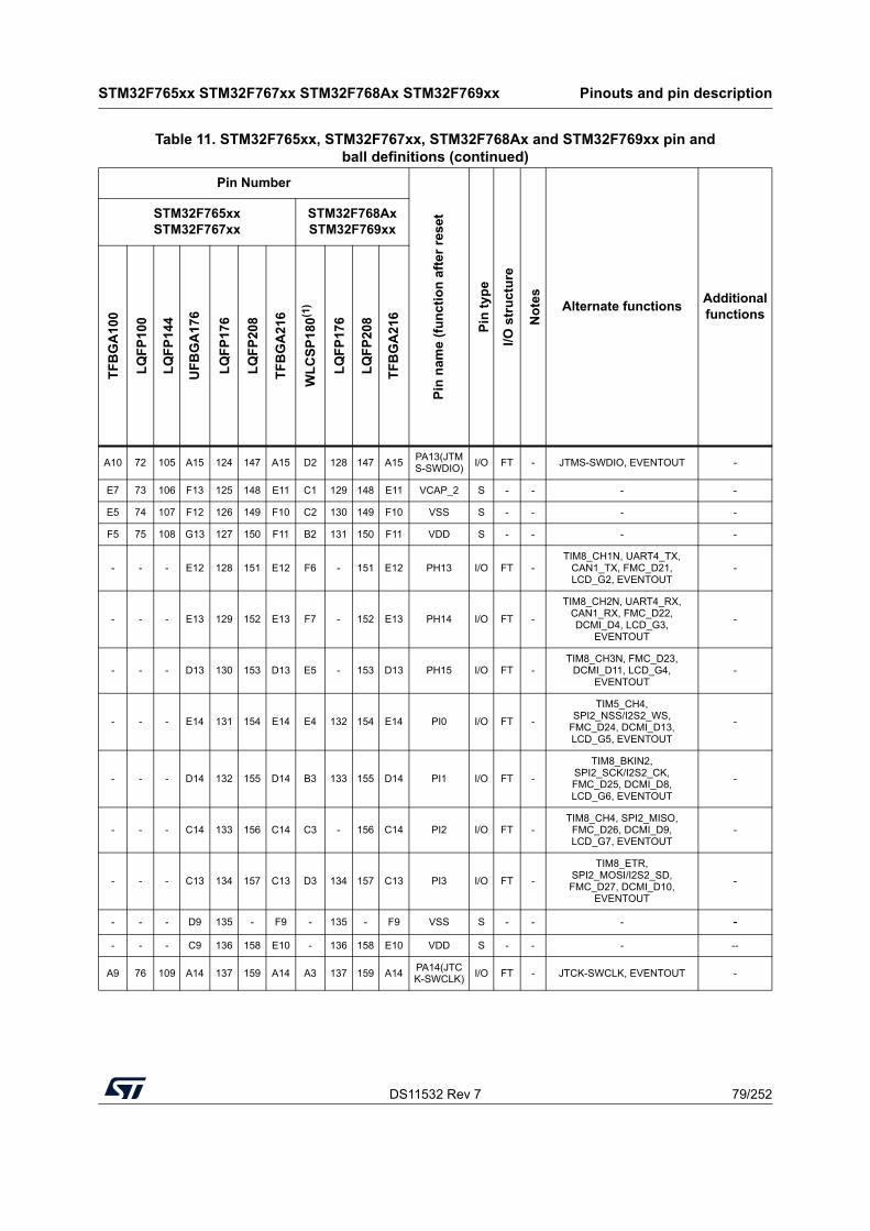
DS11532 Rev 7 79/252
STM32F765xx STM32F767xx STM32F768Ax STM32F769xx Pinouts and pin description
102
A10 72 105 A15 124 147 A15 D2 128 147 A15PA13(JTMS-SWDIO)
I/O FT - JTMS-SWDIO, EVENTOUT -
E7 73 106 F13 125 148 E11 C1 129 148 E11 VCAP_2 S - - - -
E5 74 107 F12 126 149 F10 C2 130 149 F10 VSS S - - - -
F5 75 108 G13 127 150 F11 B2 131 150 F11 VDD S - - - -
- - - E12 128 151 E12 F6 - 151 E12 PH13 I/O FT -TIM8_CH1N, UART4_TX,
CAN1_TX, FMC_D21, LCD_G2, EVENTOUT
-
- - - E13 129 152 E13 F7 - 152 E13 PH14 I/O FT -
TIM8_CH2N, UART4_RX, CAN1_RX, FMC_D22, DCMI_D4, LCD_G3,
EVENTOUT
-
- - - D13 130 153 D13 E5 - 153 D13 PH15 I/O FT -TIM8_CH3N, FMC_D23,
DCMI_D11, LCD_G4, EVENTOUT
-
- - - E14 131 154 E14 E4 132 154 E14 PI0 I/O FT -
TIM5_CH4, SPI2_NSS/I2S2_WS,
FMC_D24, DCMI_D13, LCD_G5, EVENTOUT
-
- - - D14 132 155 D14 B3 133 155 D14 PI1 I/O FT -
TIM8_BKIN2, SPI2_SCK/I2S2_CK, FMC_D25, DCMI_D8, LCD_G6, EVENTOUT
-
- - - C14 133 156 C14 C3 - 156 C14 PI2 I/O FT -TIM8_CH4, SPI2_MISO,
FMC_D26, DCMI_D9, LCD_G7, EVENTOUT
-
- - - C13 134 157 C13 D3 134 157 C13 PI3 I/O FT -
TIM8_ETR, SPI2_MOSI/I2S2_SD, FMC_D27, DCMI_D10,
EVENTOUT
-
- - - D9 135 - F9 - 135 - F9 VSS S - - - -
- - - C9 136 158 E10 - 136 158 E10 VDD S - - - --
A9 76 109 A14 137 159 A14 A3 137 159 A14PA14(JTCK-SWCLK)
I/O FT - JTCK-SWCLK, EVENTOUT -
Table 11. STM32F765xx, STM32F767xx, STM32F768Ax and STM32F769xx pin andball definitions (continued)
Pin Number
Pin
nam
e (f
un
ctio
n a
fte
r re
set
Pin
typ
e
I/O s
tru
ctu
re
No
tes
Alternate functionsAdditional functions
STM32F765xxSTM32F767xx
STM32F768AxSTM32F769xx
TF
BG
A10
0
LQ
FP
100
LQ
FP
144
UF
BG
A1
76
LQ
FP
176
LQ
FP
208
TF
BG
A21
6
WL
CS
P18
0(1)
LQ
FP
176
LQ
FP
208
TF
BG
A21
6
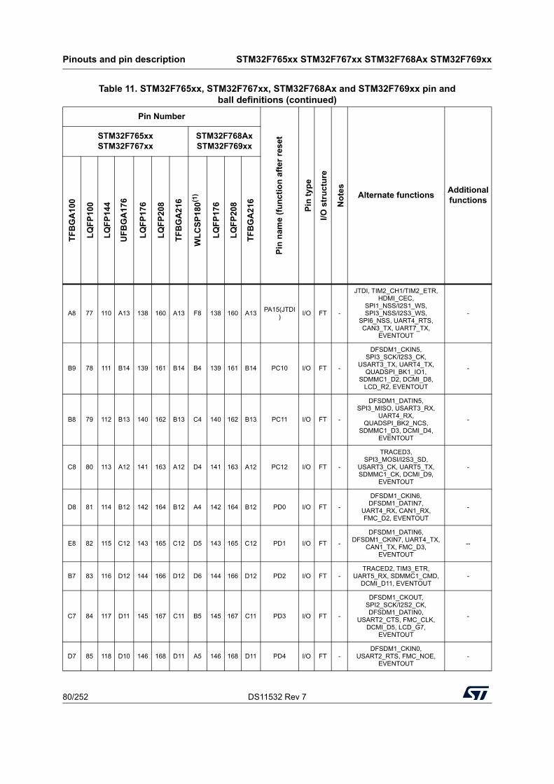
Pinouts and pin description STM32F765xx STM32F767xx STM32F768Ax STM32F769xx
80/252 DS11532 Rev 7
A8 77 110 A13 138 160 A13 F8 138 160 A13PA15(JTDI
)I/O FT -
JTDI, TIM2_CH1/TIM2_ETR, HDMI_CEC,
SPI1_NSS/I2S1_WS, SPI3_NSS/I2S3_WS,
SPI6_NSS, UART4_RTS, CAN3_TX, UART7_TX,
EVENTOUT
-
B9 78 111 B14 139 161 B14 B4 139 161 B14 PC10 I/O FT -
DFSDM1_CKIN5, SPI3_SCK/I2S3_CK,
USART3_TX, UART4_TX, QUADSPI_BK1_IO1,
SDMMC1_D2, DCMI_D8, LCD_R2, EVENTOUT
-
B8 79 112 B13 140 162 B13 C4 140 162 B13 PC11 I/O FT -
DFSDM1_DATIN5, SPI3_MISO, USART3_RX,
UART4_RX, QUADSPI_BK2_NCS,
SDMMC1_D3, DCMI_D4, EVENTOUT
-
C8 80 113 A12 141 163 A12 D4 141 163 A12 PC12 I/O FT -
TRACED3, SPI3_MOSI/I2S3_SD,
USART3_CK, UART5_TX, SDMMC1_CK, DCMI_D9,
EVENTOUT
-
D8 81 114 B12 142 164 B12 A4 142 164 B12 PD0 I/O FT -
DFSDM1_CKIN6, DFSDM1_DATIN7,
UART4_RX, CAN1_RX, FMC_D2, EVENTOUT
-
E8 82 115 C12 143 165 C12 D5 143 165 C12 PD1 I/O FT -
DFSDM1_DATIN6, DFSDM1_CKIN7, UART4_TX,
CAN1_TX, FMC_D3, EVENTOUT
--
B7 83 116 D12 144 166 D12 D6 144 166 D12 PD2 I/O FT -TRACED2, TIM3_ETR,
UART5_RX, SDMMC1_CMD, DCMI_D11, EVENTOUT
-
C7 84 117 D11 145 167 C11 B5 145 167 C11 PD3 I/O FT -
DFSDM1_CKOUT, SPI2_SCK/I2S2_CK, DFSDM1_DATIN0,
USART2_CTS, FMC_CLK, DCMI_D5, LCD_G7,
EVENTOUT
-
D7 85 118 D10 146 168 D11 A5 146 168 D11 PD4 I/O FT -DFSDM1_CKIN0,
USART2_RTS, FMC_NOE, EVENTOUT
-
Table 11. STM32F765xx, STM32F767xx, STM32F768Ax and STM32F769xx pin andball definitions (continued)
Pin Number
Pin
nam
e (f
un
ctio
n a
fte
r re
set
Pin
typ
e
I/O s
tru
ctu
re
No
tes
Alternate functionsAdditional functions
STM32F765xxSTM32F767xx
STM32F768AxSTM32F769xx
TF
BG
A10
0
LQ
FP
100
LQ
FP
144
UF
BG
A1
76
LQ
FP
176
LQ
FP
208
TF
BG
A21
6
WL
CS
P18
0(1)
LQ
FP
176
LQ
FP
208
TF
BG
A21
6
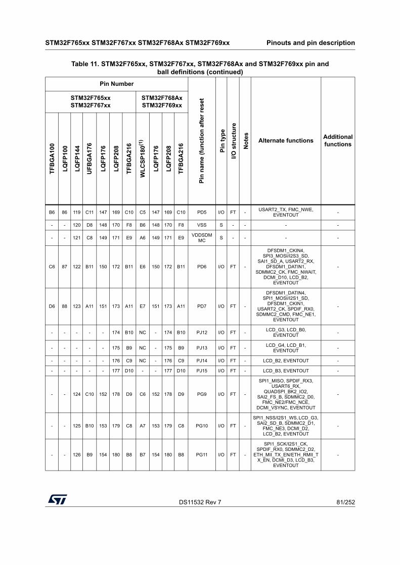
DS11532 Rev 7 81/252
STM32F765xx STM32F767xx STM32F768Ax STM32F769xx Pinouts and pin description
102
B6 86 119 C11 147 169 C10 C5 147 169 C10 PD5 I/O FT -USART2_TX, FMC_NWE,
EVENTOUT-
- - 120 D8 148 170 F8 B6 148 170 F8 VSS S - - - -
- - 121 C8 149 171 E9 A6 149 171 E9VDDSDM
MCS - - - -
C6 87 122 B11 150 172 B11 E6 150 172 B11 PD6 I/O FT -
DFSDM1_CKIN4, SPI3_MOSI/I2S3_SD,
SAI1_SD_A, USART2_RX, DFSDM1_DATIN1,
SDMMC2_CK, FMC_NWAIT, DCMI_D10, LCD_B2,
EVENTOUT
-
D6 88 123 A11 151 173 A11 E7 151 173 A11 PD7 I/O FT -
DFSDM1_DATIN4, SPI1_MOSI/I2S1_SD,
DFSDM1_CKIN1, USART2_CK, SPDIF_RX0, SDMMC2_CMD, FMC_NE1,
EVENTOUT
-
- - - - - 174 B10 NC - 174 B10 PJ12 I/O FT -LCD_G3, LCD_B0,
EVENTOUT-
- - - - - 175 B9 NC - 175 B9 PJ13 I/O FT -LCD_G4, LCD_B1,
EVENTOUT-
- - - - - 176 C9 NC - 176 C9 PJ14 I/O FT - LCD_B2, EVENTOUT -
- - - - - 177 D10 - - 177 D10 PJ15 I/O FT - LCD_B3, EVENTOUT -
- - 124 C10 152 178 D9 C6 152 178 D9 PG9 I/O FT -
SPI1_MISO, SPDIF_RX3, USART6_RX,
QUADSPI_BK2_IO2, SAI2_FS_B, SDMMC2_D0,
FMC_NE2/FMC_NCE, DCMI_VSYNC, EVENTOUT
-
- - 125 B10 153 179 C8 A7 153 179 C8 PG10 I/O FT -
SPI1_NSS/I2S1_WS, LCD_G3, SAI2_SD_B, SDMMC2_D1,
FMC_NE3, DCMI_D2, LCD_B2, EVENTOUT
-
- - 126 B9 154 180 B8 B7 154 180 B8 PG11 I/O FT -
SPI1_SCK/I2S1_CK, SPDIF_RX0, SDMMC2_D2,
ETH_MII_TX_EN/ETH_RMII_TX_EN, DCMI_D3, LCD_B3,
EVENTOUT
-
Table 11. STM32F765xx, STM32F767xx, STM32F768Ax and STM32F769xx pin andball definitions (continued)
Pin Number
Pin
nam
e (f
un
ctio
n a
fte
r re
set
Pin
typ
e
I/O s
tru
ctu
re
No
tes
Alternate functionsAdditional functions
STM32F765xxSTM32F767xx
STM32F768AxSTM32F769xx
TF
BG
A10
0
LQ
FP
100
LQ
FP
144
UF
BG
A1
76
LQ
FP
176
LQ
FP
208
TF
BG
A21
6
WL
CS
P18
0(1)
LQ
FP
176
LQ
FP
208
TF
BG
A21
6
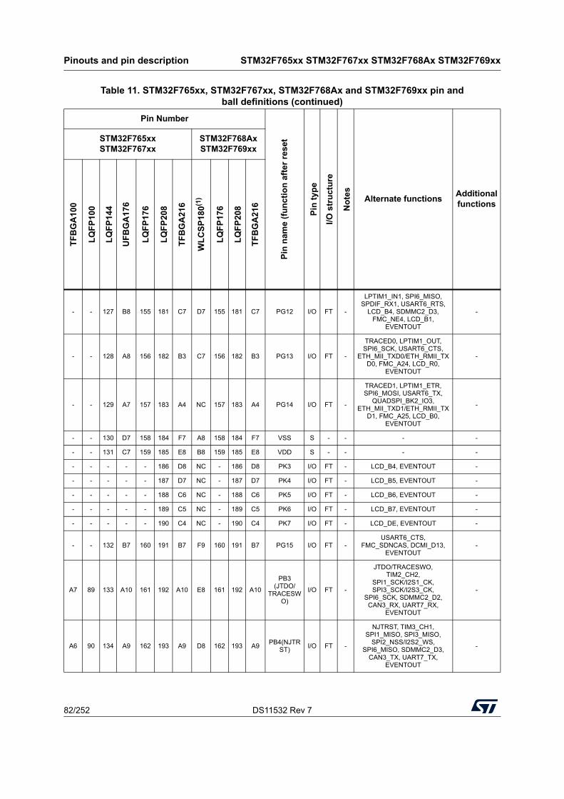
Pinouts and pin description STM32F765xx STM32F767xx STM32F768Ax STM32F769xx
82/252 DS11532 Rev 7
- - 127 B8 155 181 C7 D7 155 181 C7 PG12 I/O FT -
LPTIM1_IN1, SPI6_MISO, SPDIF_RX1, USART6_RTS,
LCD_B4, SDMMC2_D3, FMC_NE4, LCD_B1,
EVENTOUT
-
- - 128 A8 156 182 B3 C7 156 182 B3 PG13 I/O FT -
TRACED0, LPTIM1_OUT, SPI6_SCK, USART6_CTS,
ETH_MII_TXD0/ETH_RMII_TXD0, FMC_A24, LCD_R0,
EVENTOUT
-
- - 129 A7 157 183 A4 NC 157 183 A4 PG14 I/O FT -
TRACED1, LPTIM1_ETR, SPI6_MOSI, USART6_TX,
QUADSPI_BK2_IO3, ETH_MII_TXD1/ETH_RMII_TX
D1, FMC_A25, LCD_B0, EVENTOUT
-
- - 130 D7 158 184 F7 A8 158 184 F7 VSS S - - - -
- - 131 C7 159 185 E8 B8 159 185 E8 VDD S - - - -
- - - - - 186 D8 NC - 186 D8 PK3 I/O FT - LCD_B4, EVENTOUT -
- - - - - 187 D7 NC - 187 D7 PK4 I/O FT - LCD_B5, EVENTOUT -
- - - - - 188 C6 NC - 188 C6 PK5 I/O FT - LCD_B6, EVENTOUT -
- - - - - 189 C5 NC - 189 C5 PK6 I/O FT - LCD_B7, EVENTOUT -
- - - - - 190 C4 NC - 190 C4 PK7 I/O FT - LCD_DE, EVENTOUT -
- - 132 B7 160 191 B7 F9 160 191 B7 PG15 I/O FT -USART6_CTS,
FMC_SDNCAS, DCMI_D13, EVENTOUT
-
A7 89 133 A10 161 192 A10 E8 161 192 A10
PB3 (JTDO/
TRACESWO)
I/O FT -
JTDO/TRACESWO, TIM2_CH2,
SPI1_SCK/I2S1_CK, SPI3_SCK/I2S3_CK,
SPI6_SCK, SDMMC2_D2, CAN3_RX, UART7_RX,
EVENTOUT
-
A6 90 134 A9 162 193 A9 D8 162 193 A9PB4(NJTR
ST)I/O FT -
NJTRST, TIM3_CH1, SPI1_MISO, SPI3_MISO,
SPI2_NSS/I2S2_WS, SPI6_MISO, SDMMC2_D3,
CAN3_TX, UART7_TX, EVENTOUT
-
Table 11. STM32F765xx, STM32F767xx, STM32F768Ax and STM32F769xx pin andball definitions (continued)
Pin Number
Pin
nam
e (f
un
ctio
n a
fte
r re
set
Pin
typ
e
I/O s
tru
ctu
re
No
tes
Alternate functionsAdditional functions
STM32F765xxSTM32F767xx
STM32F768AxSTM32F769xx
TF
BG
A10
0
LQ
FP
100
LQ
FP
144
UF
BG
A1
76
LQ
FP
176
LQ
FP
208
TF
BG
A21
6
WL
CS
P18
0(1)
LQ
FP
176
LQ
FP
208
TF
BG
A21
6
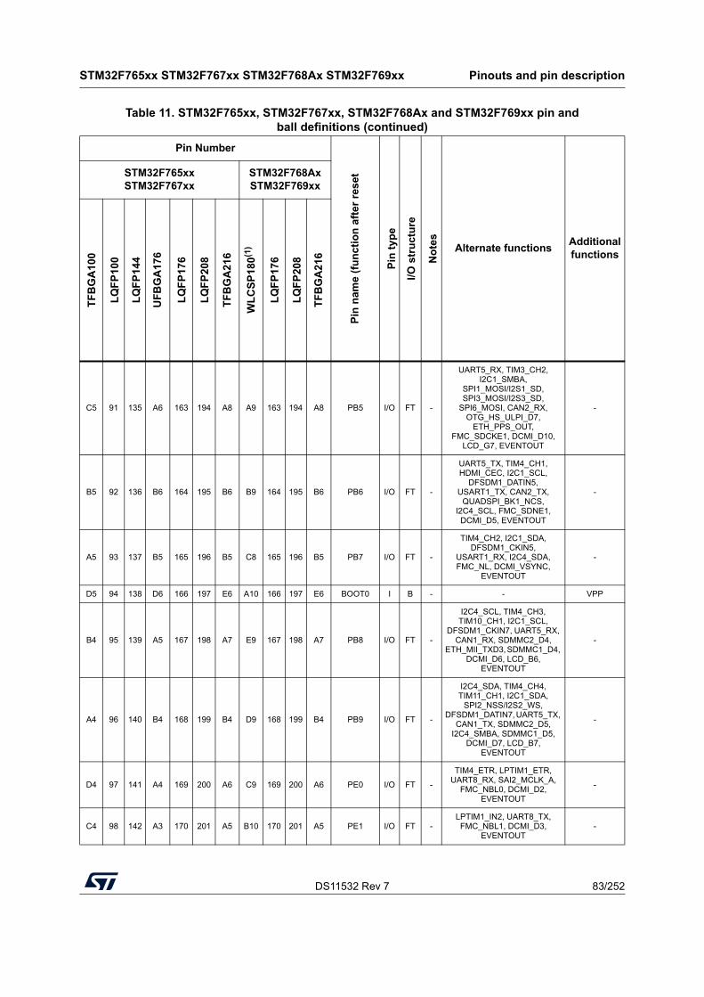
DS11532 Rev 7 83/252
STM32F765xx STM32F767xx STM32F768Ax STM32F769xx Pinouts and pin description
102
C5 91 135 A6 163 194 A8 A9 163 194 A8 PB5 I/O FT -
UART5_RX, TIM3_CH2, I2C1_SMBA,
SPI1_MOSI/I2S1_SD, SPI3_MOSI/I2S3_SD,
SPI6_MOSI, CAN2_RX, OTG_HS_ULPI_D7,
ETH_PPS_OUT, FMC_SDCKE1, DCMI_D10,
LCD_G7, EVENTOUT
-
B5 92 136 B6 164 195 B6 B9 164 195 B6 PB6 I/O FT -
UART5_TX, TIM4_CH1, HDMI_CEC, I2C1_SCL,
DFSDM1_DATIN5, USART1_TX, CAN2_TX,
QUADSPI_BK1_NCS, I2C4_SCL, FMC_SDNE1,
DCMI_D5, EVENTOUT
-
A5 93 137 B5 165 196 B5 C8 165 196 B5 PB7 I/O FT -
TIM4_CH2, I2C1_SDA, DFSDM1_CKIN5,
USART1_RX, I2C4_SDA, FMC_NL, DCMI_VSYNC,
EVENTOUT
-
D5 94 138 D6 166 197 E6 A10 166 197 E6 BOOT0 I B - - VPP
B4 95 139 A5 167 198 A7 E9 167 198 A7 PB8 I/O FT -
I2C4_SCL, TIM4_CH3, TIM10_CH1, I2C1_SCL,
DFSDM1_CKIN7, UART5_RX, CAN1_RX, SDMMC2_D4,
ETH_MII_TXD3, SDMMC1_D4, DCMI_D6, LCD_B6,
EVENTOUT
-
A4 96 140 B4 168 199 B4 D9 168 199 B4 PB9 I/O FT -
I2C4_SDA, TIM4_CH4, TIM11_CH1, I2C1_SDA,
SPI2_NSS/I2S2_WS, DFSDM1_DATIN7, UART5_TX,
CAN1_TX, SDMMC2_D5, I2C4_SMBA, SDMMC1_D5,
DCMI_D7, LCD_B7, EVENTOUT
-
D4 97 141 A4 169 200 A6 C9 169 200 A6 PE0 I/O FT -
TIM4_ETR, LPTIM1_ETR, UART8_RX, SAI2_MCLK_A,
FMC_NBL0, DCMI_D2, EVENTOUT
-
C4 98 142 A3 170 201 A5 B10 170 201 A5 PE1 I/O FT -LPTIM1_IN2, UART8_TX, FMC_NBL1, DCMI_D3,
EVENTOUT-
Table 11. STM32F765xx, STM32F767xx, STM32F768Ax and STM32F769xx pin andball definitions (continued)
Pin Number
Pin
nam
e (f
un
ctio
n a
fte
r re
set
Pin
typ
e
I/O s
tru
ctu
re
No
tes
Alternate functionsAdditional functions
STM32F765xxSTM32F767xx
STM32F768AxSTM32F769xx
TF
BG
A10
0
LQ
FP
100
LQ
FP
144
UF
BG
A1
76
LQ
FP
176
LQ
FP
208
TF
BG
A21
6
WL
CS
P18
0(1)
LQ
FP
176
LQ
FP
208
TF
BG
A21
6
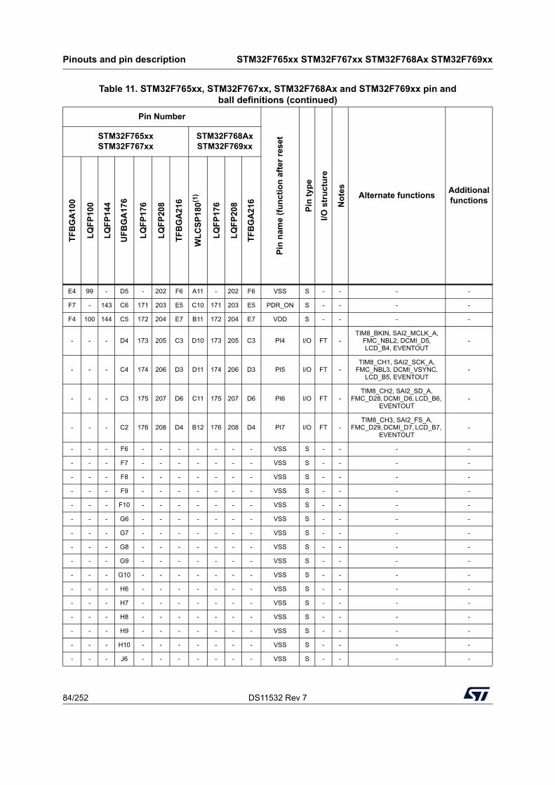
Pinouts and pin description STM32F765xx STM32F767xx STM32F768Ax STM32F769xx
84/252 DS11532 Rev 7
E4 99 - D5 - 202 F6 A11 - 202 F6 VSS S - - - -
F7 - 143 C6 171 203 E5 C10 171 203 E5 PDR_ON S - - - -
F4 100 144 C5 172 204 E7 B11 172 204 E7 VDD S - - - -
- - - D4 173 205 C3 D10 173 205 C3 PI4 I/O FT -TIM8_BKIN, SAI2_MCLK_A,
FMC_NBL2, DCMI_D5, LCD_B4, EVENTOUT
-
- - - C4 174 206 D3 D11 174 206 D3 PI5 I/O FT -TIM8_CH1, SAI2_SCK_A,
FMC_NBL3, DCMI_VSYNC, LCD_B5, EVENTOUT
-
- - - C3 175 207 D6 C11 175 207 D6 PI6 I/O FT -TIM8_CH2, SAI2_SD_A,
FMC_D28, DCMI_D6, LCD_B6, EVENTOUT
-
- - - C2 176 208 D4 B12 176 208 D4 PI7 I/O FT -TIM8_CH3, SAI2_FS_A,
FMC_D29, DCMI_D7, LCD_B7, EVENTOUT
-
- - - F6 - - - - - - - VSS S - - - -
- - - F7 - - - - - - - VSS S - - - -
- - - F8 - - - - - - - VSS S - - - -
- - - F9 - - - - - - - VSS S - - - -
- - - F10 - - - - - - - VSS S - - - -
- - - G6 - - - - - - - VSS S - - - -
- - - G7 - - - - - - - VSS S - - - -
- - - G8 - - - - - - - VSS S - - - -
- - - G9 - - - - - - - VSS S - - - -
- - - G10 - - - - - - - VSS S - - - -
- - - H6 - - - - - - - VSS S - - - -
- - - H7 - - - - - - - VSS S - - - -
- - - H8 - - - - - - - VSS S - - - -
- - - H9 - - - - - - - VSS S - - - -
- - - H10 - - - - - - - VSS S - - - -
- - - J6 - - - - - - - VSS S - - - -
Table 11. STM32F765xx, STM32F767xx, STM32F768Ax and STM32F769xx pin andball definitions (continued)
Pin Number
Pin
nam
e (f
un
ctio
n a
fte
r re
set
Pin
typ
e
I/O s
tru
ctu
re
No
tes
Alternate functionsAdditional functions
STM32F765xxSTM32F767xx
STM32F768AxSTM32F769xx
TF
BG
A10
0
LQ
FP
100
LQ
FP
144
UF
BG
A1
76
LQ
FP
176
LQ
FP
208
TF
BG
A21
6
WL
CS
P18
0(1)
LQ
FP
176
LQ
FP
208
TF
BG
A21
6
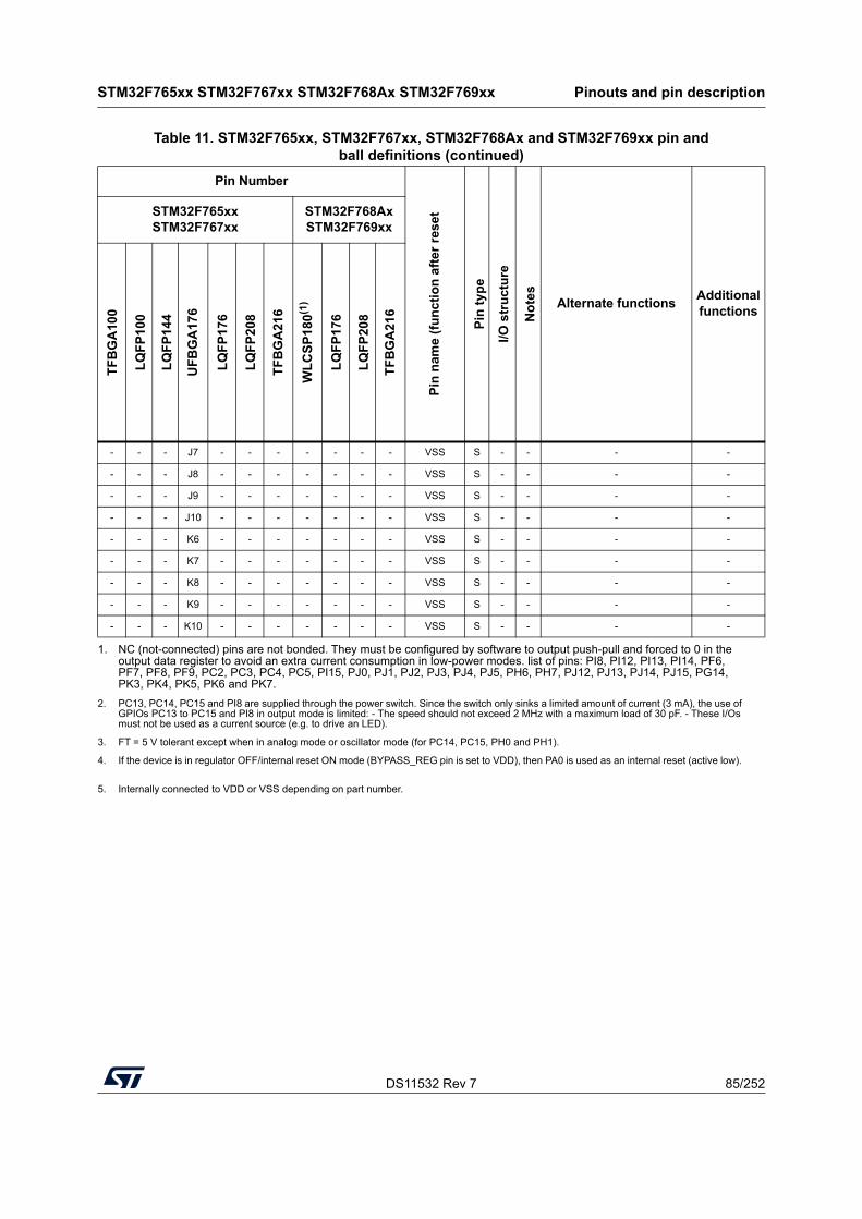
DS11532 Rev 7 85/252
STM32F765xx STM32F767xx STM32F768Ax STM32F769xx Pinouts and pin description
102
- - - J7 - - - - - - - VSS S - - - -
- - - J8 - - - - - - - VSS S - - - -
- - - J9 - - - - - - - VSS S - - - -
- - - J10 - - - - - - - VSS S - - - -
- - - K6 - - - - - - - VSS S - - - -
- - - K7 - - - - - - - VSS S - - - -
- - - K8 - - - - - - - VSS S - - - -
- - - K9 - - - - - - - VSS S - - - -
- - - K10 - - - - - - - VSS S - - - -
1. NC (not-connected) pins are not bonded. They must be configured by software to output push-pull and forced to 0 in the output data register to avoid an extra current consumption in low-power modes. list of pins: PI8, PI12, PI13, PI14, PF6, PF7, PF8, PF9, PC2, PC3, PC4, PC5, PI15, PJ0, PJ1, PJ2, PJ3, PJ4, PJ5, PH6, PH7, PJ12, PJ13, PJ14, PJ15, PG14, PK3, PK4, PK5, PK6 and PK7.
2. PC13, PC14, PC15 and PI8 are supplied through the power switch. Since the switch only sinks a limited amount of current (3 mA), the use of GPIOs PC13 to PC15 and PI8 in output mode is limited: - The speed should not exceed 2 MHz with a maximum load of 30 pF. - These I/Os must not be used as a current source (e.g. to drive an LED).
3. FT = 5 V tolerant except when in analog mode or oscillator mode (for PC14, PC15, PH0 and PH1).
4. If the device is in regulator OFF/internal reset ON mode (BYPASS_REG pin is set to VDD), then PA0 is used as an internal reset (active low).
5. Internally connected to VDD or VSS depending on part number.
Table 11. STM32F765xx, STM32F767xx, STM32F768Ax and STM32F769xx pin andball definitions (continued)
Pin Number
Pin
nam
e (f
un
ctio
n a
fte
r re
set
Pin
typ
e
I/O s
tru
ctu
re
No
tes
Alternate functionsAdditional functions
STM32F765xxSTM32F767xx
STM32F768AxSTM32F769xx
TF
BG
A10
0
LQ
FP
100
LQ
FP
144
UF
BG
A1
76
LQ
FP
176
LQ
FP
208
TF
BG
A21
6
WL
CS
P18
0(1)
LQ
FP
176
LQ
FP
208
TF
BG
A21
6
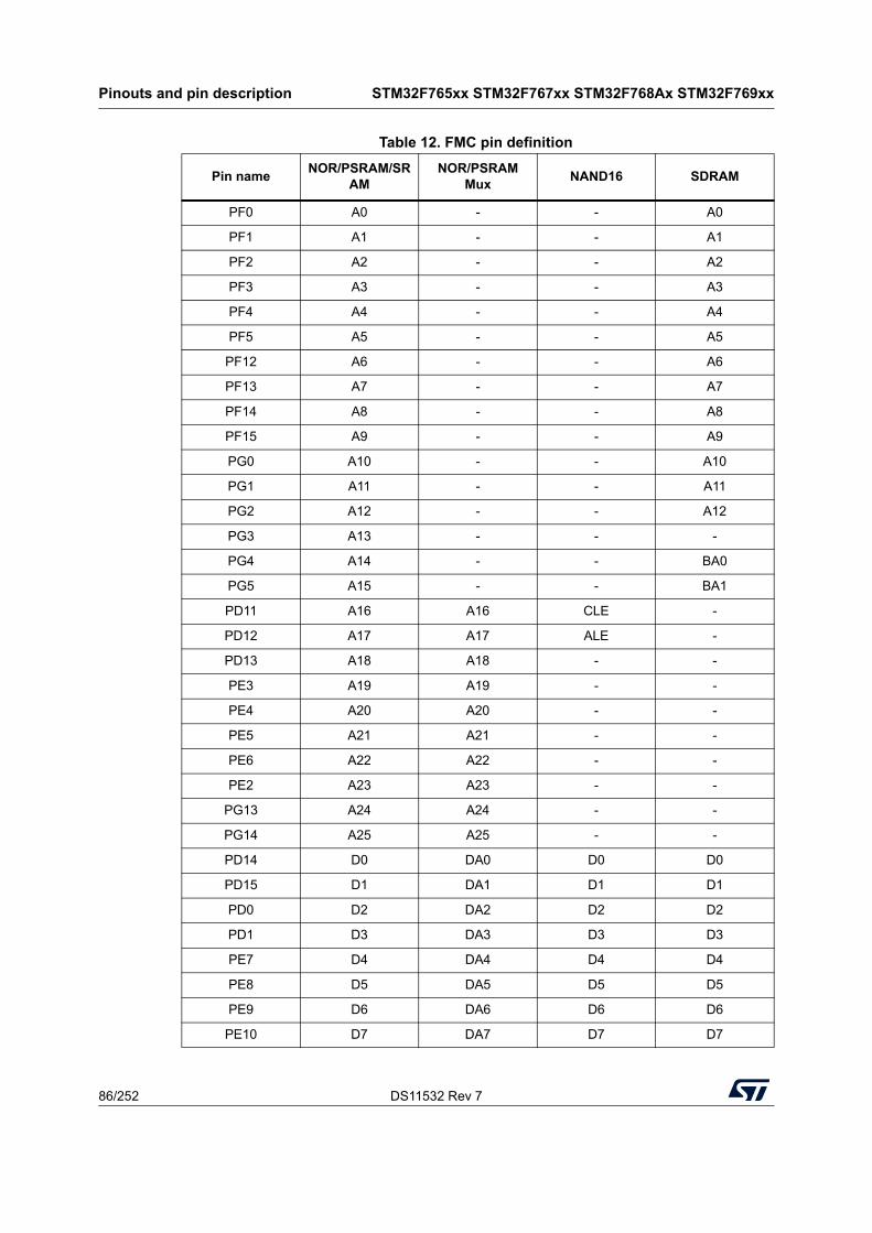
Pinouts and pin description STM32F765xx STM32F767xx STM32F768Ax STM32F769xx
86/252 DS11532 Rev 7
Table 12. FMC pin definition
Pin nameNOR/PSRAM/SR
AMNOR/PSRAM
MuxNAND16 SDRAM
PF0 A0 - - A0
PF1 A1 - - A1
PF2 A2 - - A2
PF3 A3 - - A3
PF4 A4 - - A4
PF5 A5 - - A5
PF12 A6 - - A6
PF13 A7 - - A7
PF14 A8 - - A8
PF15 A9 - - A9
PG0 A10 - - A10
PG1 A11 - - A11
PG2 A12 - - A12
PG3 A13 - - -
PG4 A14 - - BA0
PG5 A15 - - BA1
PD11 A16 A16 CLE -
PD12 A17 A17 ALE -
PD13 A18 A18 - -
PE3 A19 A19 - -
PE4 A20 A20 - -
PE5 A21 A21 - -
PE6 A22 A22 - -
PE2 A23 A23 - -
PG13 A24 A24 - -
PG14 A25 A25 - -
PD14 D0 DA0 D0 D0
PD15 D1 DA1 D1 D1
PD0 D2 DA2 D2 D2
PD1 D3 DA3 D3 D3
PE7 D4 DA4 D4 D4
PE8 D5 DA5 D5 D5
PE9 D6 DA6 D6 D6
PE10 D7 DA7 D7 D7
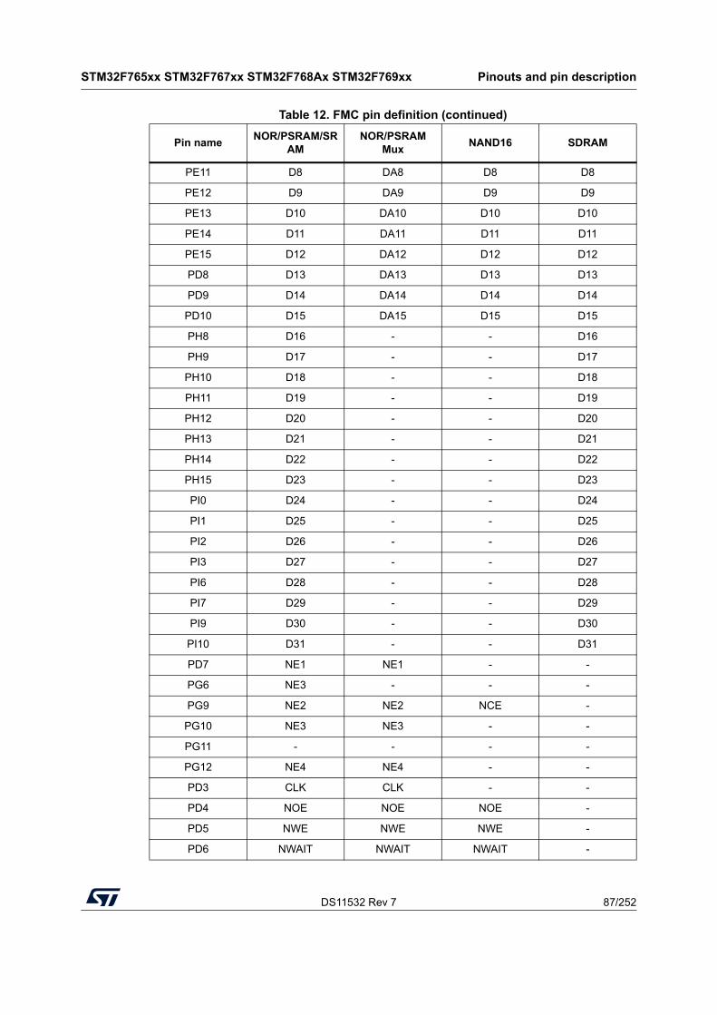
DS11532 Rev 7 87/252
STM32F765xx STM32F767xx STM32F768Ax STM32F769xx Pinouts and pin description
102
PE11 D8 DA8 D8 D8
PE12 D9 DA9 D9 D9
PE13 D10 DA10 D10 D10
PE14 D11 DA11 D11 D11
PE15 D12 DA12 D12 D12
PD8 D13 DA13 D13 D13
PD9 D14 DA14 D14 D14
PD10 D15 DA15 D15 D15
PH8 D16 - - D16
PH9 D17 - - D17
PH10 D18 - - D18
PH11 D19 - - D19
PH12 D20 - - D20
PH13 D21 - - D21
PH14 D22 - - D22
PH15 D23 - - D23
PI0 D24 - - D24
PI1 D25 - - D25
PI2 D26 - - D26
PI3 D27 - - D27
PI6 D28 - - D28
PI7 D29 - - D29
PI9 D30 - - D30
PI10 D31 - - D31
PD7 NE1 NE1 - -
PG6 NE3 - - -
PG9 NE2 NE2 NCE -
PG10 NE3 NE3 - -
PG11 - - - -
PG12 NE4 NE4 - -
PD3 CLK CLK - -
PD4 NOE NOE NOE -
PD5 NWE NWE NWE -
PD6 NWAIT NWAIT NWAIT -
Table 12. FMC pin definition (continued)
Pin nameNOR/PSRAM/SR
AMNOR/PSRAM
MuxNAND16 SDRAM
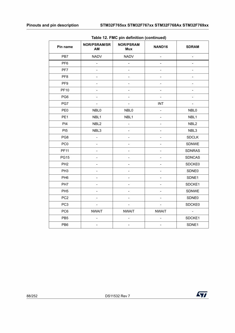
Pinouts and pin description STM32F765xx STM32F767xx STM32F768Ax STM32F769xx
88/252 DS11532 Rev 7
PB7 NADV NADV - -
PF6 - - - -
PF7 - - - -
PF8 - - - -
PF9 - - - -
PF10 - - - -
PG6 - - - -
PG7 - - INT -
PE0 NBL0 NBL0 - NBL0
PE1 NBL1 NBL1 - NBL1
PI4 NBL2 - - NBL2
PI5 NBL3 - - NBL3
PG8 - - - SDCLK
PC0 - - - SDNWE
PF11 - - - SDNRAS
PG15 - - - SDNCAS
PH2 - - - SDCKE0
PH3 - - - SDNE0
PH6 - - - SDNE1
PH7 - - - SDCKE1
PH5 - - - SDNWE
PC2 - - - SDNE0
PC3 - - - SDCKE0
PC6 NWAIT NWAIT NWAIT -
PB5 - - - SDCKE1
PB6 - - - SDNE1
Table 12. FMC pin definition (continued)
Pin nameNOR/PSRAM/SR
AMNOR/PSRAM
MuxNAND16 SDRAM
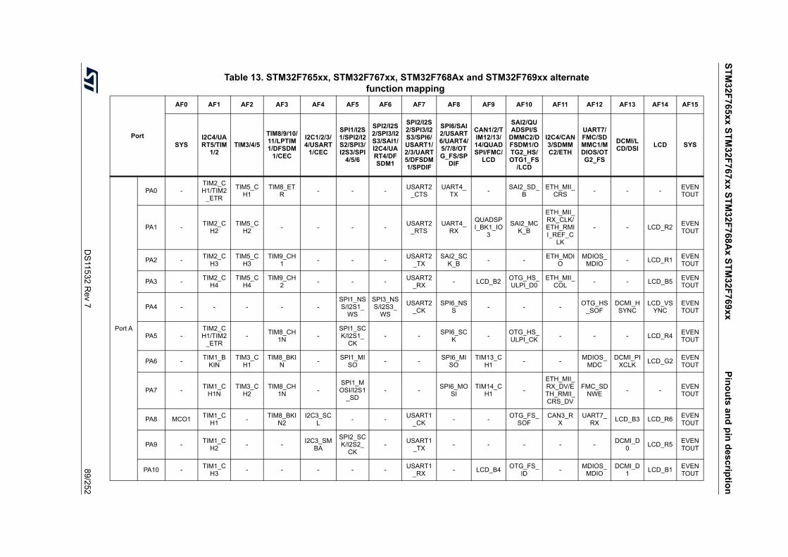
ST
M3
2F7
65xx
ST
M3
2F7
67xx
ST
M3
2F7
68A
x S
TM
32F
769
xxP
ino
uts
an
d p
in d
esc
riptio
n
DS
11532 R
ev 789/252
Table 13. STM32F765xx, STM32F767xx, STM32F768Ax and STM32F769xx alternatefunction mapping
Port
AF0 AF1 AF2 AF3 AF4 AF5 AF6 AF7 AF8 AF9 AF10 AF11 AF12 AF13 AF14 AF15
SYSI2C4/UART5/TIM
1/2TIM3/4/5
TIM8/9/10/11/LPTIM1/DFSDM
1/CEC
I2C1/2/3/4/USART
1/CEC
SPI1/I2S1/SPI2/I2S2/SPI3/I2S3/SPI
4/5/6
SPI2/I2S2/SPI3/I2S3/SAI1/I2C4/UART4/DFSDM1
SPI2/I2S2/SPI3/I2S3/SPI6/USART1/2/3/UART5/DFSDM1/SPDIF
SPI6/SAI2/USART6/UART4/5/7/8/OTG_FS/SP
DIF
CAN1/2/TIM12/13/14/QUADSPI/FMC/
LCD
SAI2/QUADSPI/S
DMMC2/DFSDM1/OTG2_HS/OTG1_FS
/LCD
I2C4/CAN3/SDMMC2/ETH
UART7/FMC/SDMMC1/MDIOS/OTG2_FS
DCMI/LCD/DSI
LCD SYS
Port A
PA0 -TIM2_CH1/TIM2
_ETR
TIM5_CH1
TIM8_ETR
- - -USART2
_CTSUART4_
TX-
SAI2_SD_B
ETH_MII_CRS
- - -EVENTOUT
PA1 -TIM2_C
H2TIM5_C
H2- - - -
USART2_RTS
UART4_RX
QUADSPI_BK1_IO
3
SAI2_MCK_B
ETH_MII_RX_CLK/ETH_RMII_REF_C
LK
- - LCD_R2EVENTOUT
PA2 -TIM2_C
H3TIM5_C
H3TIM9_CH
1- - -
USART2_TX
SAI2_SCK_B
- -ETH_MDI
OMDIOS_
MDIO- LCD_R1
EVENTOUT
PA3 -TIM2_C
H4TIM5_C
H4TIM9_CH
2- - -
USART2_RX
- LCD_B2OTG_HS_ULPI_D0
ETH_MII_COL
- - LCD_B5EVENTOUT
PA4 - - - - -SPI1_NSS/I2S1_
WS
SPI3_NSS/I2S3_
WS
USART2_CK
SPI6_NSS
- - -OTG_HS
_SOFDCMI_HSYNC
LCD_VSYNC
EVENTOUT
PA5 -TIM2_CH1/TIM2
_ETR-
TIM8_CH1N
-SPI1_SCK/I2S1_
CK- -
SPI6_SCK
-OTG_HS_ULPI_CK
- - - LCD_R4EVENTOUT
PA6 -TIM1_B
KINTIM3_C
H1TIM8_BKI
N-
SPI1_MISO
- -SPI6_MI
SOTIM13_C
H1- -
MDIOS_MDC
DCMI_PIXCLK
LCD_G2EVENTOUT
PA7 -TIM1_C
H1NTIM3_C
H2TIM8_CH
1N-
SPI1_MOSI/I2S1
_SD- -
SPI6_MOSI
TIM14_CH1
-
ETH_MII_RX_DV/ETH_RMII_CRS_DV
FMC_SDNWE
- -EVENTOUT
PA8 MCO1TIM1_C
H1-
TIM8_BKIN2
I2C3_SCL
- -USART1
_CK- -
OTG_FS_SOF
CAN3_RX
UART7_RX
LCD_B3 LCD_R6EVENTOUT
PA9 -TIM1_C
H2- -
I2C3_SMBA
SPI2_SCK/I2S2_
CK-
USART1_TX
- - - - -DCMI_D
0LCD_R5
EVENTOUT
PA10 -TIM1_C
H3- - - - -
USART1_RX
- LCD_B4OTG_FS_
ID-
MDIOS_MDIO
DCMI_D1
LCD_B1EVENTOUT
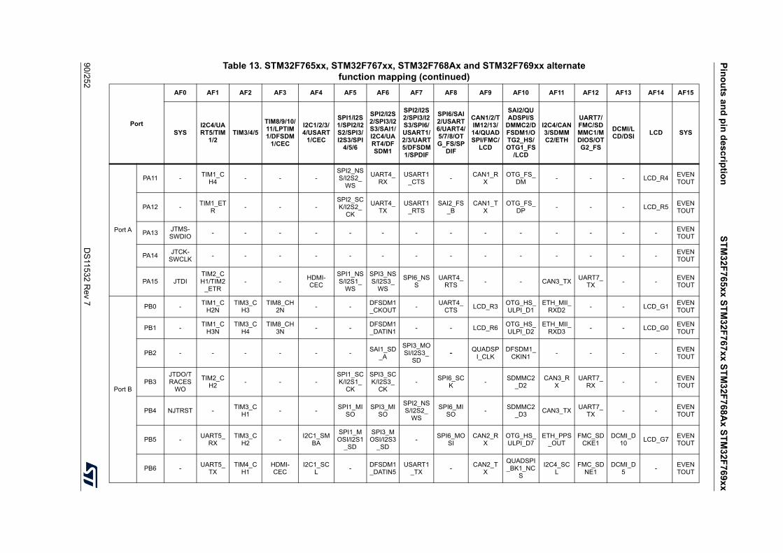
Pin
ou
ts a
nd
pin
de
scrip
tion
ST
M32
F76
5xx
ST
M32
F76
7xx
ST
M3
2F7
68A
x S
TM
32F
769x
x
90/2
52D
S115
32 Rev 7
Port A
PA11 -TIM1_C
H4- - -
SPI2_NSS/I2S2_
WS
UART4_RX
USART1_CTS
-CAN1_R
XOTG_FS_
DM- - - LCD_R4
EVENTOUT
PA12 -TIM1_ET
R- - -
SPI2_SCK/I2S2_
CK
UART4_TX
USART1_RTS
SAI2_FS_B
CAN1_TX
OTG_FS_DP
- - - LCD_R5EVENTOUT
PA13JTMS-SWDIO
- - - - - - - - - - - - - -EVENTOUT
PA14JTCK-
SWCLK- - - - - - - - - - - - - -
EVENTOUT
PA15 JTDITIM2_CH1/TIM2
_ETR- -
HDMI-CEC
SPI1_NSS/I2S1_
WS
SPI3_NSS/I2S3_
WS
SPI6_NSS
UART4_RTS
- - CAN3_TXUART7_
TX- -
EVENTOUT
Port B
PB0 -TIM1_C
H2NTIM3_C
H3TIM8_CH
2N- -
DFSDM1_CKOUT
-UART4_
CTSLCD_R3
OTG_HS_ULPI_D1
ETH_MII_RXD2
- - LCD_G1EVENTOUT
PB1 -TIM1_C
H3NTIM3_C
H4TIM8_CH
3N- -
DFSDM1_DATIN1
- - LCD_R6OTG_HS_ULPI_D2
ETH_MII_RXD3
- - LCD_G0EVENTOUT
PB2 - - - - - -SAI1_SD
_A
SPI3_MOSI/I2S3_
SD- QUADSP
I_CLKDFSDM1_
CKIN1- - - -
EVENTOUT
PB3JTDO/TRACES
WO
TIM2_CH2
- - -SPI1_SCK/I2S1_
CK
SPI3_SCK/I2S3_
CK-
SPI6_SCK
-SDMMC2
_D2CAN3_R
XUART7_
RX- -
EVENTOUT
PB4 NJTRST -TIM3_C
H1- -
SPI1_MISO
SPI3_MISO
SPI2_NSS/I2S2_
WS
SPI6_MISO
-SDMMC2
_D3CAN3_TX
UART7_TX
- -EVENTOUT
PB5 -UART5_
RXTIM3_C
H2-
I2C1_SMBA
SPI1_MOSI/I2S1
_SD
SPI3_MOSI/I2S3
_SD-
SPI6_MOSI
CAN2_RX
OTG_HS_ULPI_D7
ETH_PPS_OUT
FMC_SDCKE1
DCMI_D10
LCD_G7EVENTOUT
PB6 -UART5_
TXTIM4_C
H1HDMI-CEC
I2C1_SCL
-DFSDM1_DATIN5
USART1_TX
-CAN2_T
X
QUADSPI_BK1_NC
S
I2C4_SCL
FMC_SDNE1
DCMI_D5
-EVENTOUT
Table 13. STM32F765xx, STM32F767xx, STM32F768Ax and STM32F769xx alternatefunction mapping (continued)
Port
AF0 AF1 AF2 AF3 AF4 AF5 AF6 AF7 AF8 AF9 AF10 AF11 AF12 AF13 AF14 AF15
SYSI2C4/UART5/TIM
1/2TIM3/4/5
TIM8/9/10/11/LPTIM1/DFSDM
1/CEC
I2C1/2/3/4/USART
1/CEC
SPI1/I2S1/SPI2/I2S2/SPI3/I2S3/SPI
4/5/6
SPI2/I2S2/SPI3/I2S3/SAI1/I2C4/UART4/DFSDM1
SPI2/I2S2/SPI3/I2S3/SPI6/USART1/2/3/UART5/DFSDM1/SPDIF
SPI6/SAI2/USART6/UART4/5/7/8/OTG_FS/SP
DIF
CAN1/2/TIM12/13/14/QUADSPI/FMC/
LCD
SAI2/QUADSPI/S
DMMC2/DFSDM1/OTG2_HS/OTG1_FS
/LCD
I2C4/CAN3/SDMMC2/ETH
UART7/FMC/SDMMC1/MDIOS/OTG2_FS
DCMI/LCD/DSI
LCD SYS
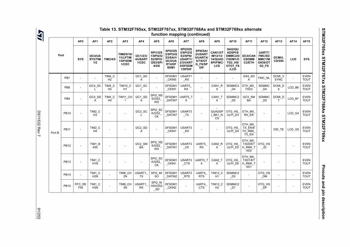
ST
M3
2F7
65xx
ST
M3
2F7
67xx
ST
M3
2F7
68A
x S
TM
32F
769
xxP
ino
uts
an
d p
in d
esc
riptio
n
DS
11532 R
ev 791/252
Port B
PB7 - -TIM4_C
H2-
I2C1_SDA
-DFSDM1_CKIN5
USART1_RX
- - -I2S4_SD
AFMC_NL
DCMI_VSYNC
-EVENTOUT
PB8 -I2C4_SC
LTIM4_C
H3TIM10_C
H1I2C1_SC
L-
DFSDM1_CKIN7
UART5_RX
-CAN1_R
XSDMMC2
_D4ETH_MII_
TXD3SDMMC
_D4DCMI_D
6LCD_B6
EVENTOUT
PB9 -I2C4_SD
ATIM4_C
H4TIM11_CH
1I2C1_SD
A
SPI2_NSS/I2S2_
WS
DFSDM1_DATIN7
UART5_TX
-CAN1_T
XSDMMC2
_D5I2C4_SM
BASDMMC
_D5DCMI_D
7LCD_B7
EVENTOUT
PB10 -TIM2_C
H3- -
I2C2_SCL
SPI2_SCK/I2S2_
CK
DFSDM1_DATIN7
USART3_TX
-
-QUADSPI_BK1_N
CS
OTG_HS_ULPI_D3
ETH_MII_RX_ER
- - LCD_G4EVENTOUT
PB11 -TIM2_C
H4- -
I2C2_SDA
-DFSDM1_CKIN7
USART3_RX
- -OTG_HS_ULPI_D4
ETH_MII_TX_EN/ETH_RMII_
TX_EN
- DSI_TE LCD_G5EVENTOUT
PB12 -TIM1_B
KIN- -
I2C2_SMBA
SPI2_NSS/I2S2_
WS
DFSDM1_DATIN1
USART3_CK
UART5_RX
CAN2_RX
OTG_HS_ULPI_D5
ETH_MII_TXD0/ETH_RMII_T
XD0
OTG_HS_ID
- -EVENTOUT
PB13 -TIM1_C
H1N- - -
SPI2_SCK/I2S2_
CK
DFSDM1_CKIN1
USART3_CTS
UART5_TX
CAN2_TX
OTG_HS_ULPI_D6
ETH_MII_TXD1/ETH_RMII_T
XD1
- - -EVENTOUT
PB14 -TIM1_C
H2N-
TIM8_CH2N
USART1_TX
SPI2_MISO
DFSDM1_DATIN2
USART3_RTS
UART4_RTS
TIM12_CH1
SDMMC2_D0
-OTG_HS
_DM- -
EVENTOUT
PB15RTC_RE
FINTIM1_C
H3N-
TIM8_CH3N
USART1_RX
SPI2_MOSI/I2S2
_SD
DFSDM1_CKIN2
-UART4_
CTSTIM12_C
H2SDMMC2
_D1-
OTG_HS_DP
- -EVENTOUT
Table 13. STM32F765xx, STM32F767xx, STM32F768Ax and STM32F769xx alternatefunction mapping (continued)
Port
AF0 AF1 AF2 AF3 AF4 AF5 AF6 AF7 AF8 AF9 AF10 AF11 AF12 AF13 AF14 AF15
SYSI2C4/UART5/TIM
1/2TIM3/4/5
TIM8/9/10/11/LPTIM1/DFSDM
1/CEC
I2C1/2/3/4/USART
1/CEC
SPI1/I2S1/SPI2/I2S2/SPI3/I2S3/SPI
4/5/6
SPI2/I2S2/SPI3/I2S3/SAI1/I2C4/UART4/DFSDM1
SPI2/I2S2/SPI3/I2S3/SPI6/USART1/2/3/UART5/DFSDM1/SPDIF
SPI6/SAI2/USART6/UART4/5/7/8/OTG_FS/SP
DIF
CAN1/2/TIM12/13/14/QUADSPI/FMC/
LCD
SAI2/QUADSPI/S
DMMC2/DFSDM1/OTG2_HS/OTG1_FS
/LCD
I2C4/CAN3/SDMMC2/ETH
UART7/FMC/SDMMC1/MDIOS/OTG2_FS
DCMI/LCD/DSI
LCD SYS
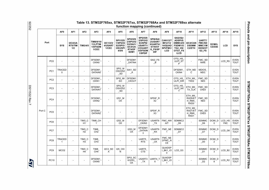
Pin
ou
ts a
nd
pin
de
scrip
tion
ST
M32
F76
5xx
ST
M32
F76
7xx
ST
M3
2F7
68A
x S
TM
32F
769x
x
92/2
52D
S115
32 Rev 7
Port C
PC0 - - -DFSDM1_
CKIN0- -
DFSDM1_DATIN4
-SAI2_FS
_B-
OTG_HS_ULPI_ST
P-
FMC_SDNWE
- LCD_R5EVENTOUT
PC1TRACED
0- -
DFSDM1_DATAIN0
-SPI2_MOSI/I2S2
_SD
SAI1_SD_A
- - -DFSDM1_
CKIN4ETH_MD
CMDIOS_
MDC- -
EVENTOUT
PC2 - - -DFSDM1_
CKIN1-
SPI2_MISO
DFSDM1_CKOUT
- - -OTG_HS_ULPI_DIR
ETH_MII_TXD2
FMC_SDNE0
- -EVENTOUT
PC3 - - -DFSDM1_DATAIN1
-SPI2_MOSI/I2S2
_SD- - - -
OTG_HS_ULPI_NX
T
ETH_MII_TX_CLK
FMC_SDCKE0
- -EVENTOUT
PC4 - - -DFSDM1_
CKIN2-
I2S1_MCK
- -SPDIF_R
X2- -
ETH_MII_RXD0/ETH_RMII_
RXD0
FMC_SDNE0
- -EVENTOUT
PC5 - - -DFSDM1_DATAIN2
- - - -SPDIF_R
X3- -
ETH_MII_RXD1/ETH_RMII_
RXD1
FMC_SDCKE0
- -EVENTOUT
PC6 - -TIM3_C
H1TIM8_CH
1-
I2S2_MCK
-DFSDM1_CKIN3
USART6_TX
FMC_NWAIT
SDMMC2_D6
-SDMMC
_D6DCMI_D
0LCD_HS
YNCEVENTOUT
PC7 - -TIM3_C
H2TIM8_CH2
- -I2S3_M
CK
DFSDM1_DATAIN
3
USART6_RX
FMC_NE1
SDMMC2_D7
-SDMMC
_D7DCMI_D
1LCD_G6
EVENTOUT
PC8TRACED
1-
TIM3_CH3
TIM8_CH3
- - -UART5_
RTSUSART6
_CK
FMC_NE2/FMC_N
CE- -
SDMMC_D0
DCMI_D2
-EVENTOUT
PC9 MCO2 -TIM3_C
H4TIM8_CH4
I2C3_SDA
I2S_CKIN
-UART5_
CTS-
QUADSPI_BK1_IO
0LCD_G3 -
SDMMC_D1
DCMI_D3
LCD_B2EVENTOUT
PC10 - - -DFSDM1_
CKIN5- -
SPI3_SCK/I2S3_
CK
USART3_TX
UART4_TX
QUADSPI_BK1_IO
1- -
SDMMC_D2
DCMI_D8
LCD_R2EVENTOUT
Table 13. STM32F765xx, STM32F767xx, STM32F768Ax and STM32F769xx alternatefunction mapping (continued)
Port
AF0 AF1 AF2 AF3 AF4 AF5 AF6 AF7 AF8 AF9 AF10 AF11 AF12 AF13 AF14 AF15
SYSI2C4/UART5/TIM
1/2TIM3/4/5
TIM8/9/10/11/LPTIM1/DFSDM
1/CEC
I2C1/2/3/4/USART
1/CEC
SPI1/I2S1/SPI2/I2S2/SPI3/I2S3/SPI
4/5/6
SPI2/I2S2/SPI3/I2S3/SAI1/I2C4/UART4/DFSDM1
SPI2/I2S2/SPI3/I2S3/SPI6/USART1/2/3/UART5/DFSDM1/SPDIF
SPI6/SAI2/USART6/UART4/5/7/8/OTG_FS/SP
DIF
CAN1/2/TIM12/13/14/QUADSPI/FMC/
LCD
SAI2/QUADSPI/S
DMMC2/DFSDM1/OTG2_HS/OTG1_FS
/LCD
I2C4/CAN3/SDMMC2/ETH
UART7/FMC/SDMMC1/MDIOS/OTG2_FS
DCMI/LCD/DSI
LCD SYS
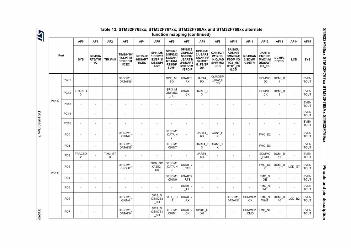
ST
M3
2F7
65xx
ST
M3
2F7
67xx
ST
M3
2F7
68A
x S
TM
32F
769
xxP
ino
uts
an
d p
in d
esc
riptio
n
DS
11532 R
ev 793/252
Port C
PC11 - - -DFSDM1_DATAIN5
- -SPI3_MI
SOUSART3
_RXUART4_
RX
QUADSPI_BK2_N
CS- -
SDMMC_D3
DCMI_D4
-EVENTOUT
PC12TRACED
3- - - - -
SPI3_MOSI/I2S3
_SD
USART3_CK
UART5_TX
- - -SDMMC
_CKDCMI_D
9-
EVENTOUT
PC13 - - - - - - - - - - - - - - -EVENTOUT
PC14 - - - - - - - - - - - - - - -EVENTOUT
PC15 - - - - - - - - - - - - - - -EVENTOUT
Port D
PD0 - - -DFSDM1_
CKIN6- -
DFSDM1_DATAIN
7-
UART4_RX
CAN1_RX
- - FMC_D2 - -EVENTOUT
PD1 - - -DFSDM1_DATAIN6
- -DFSDM1_CKIN7
-UART4_T
XCAN1_T
X- - FMC_D3 - -
EVENTOUT
PD2TRACED
2-
TIM3_ETR
- - - - -UART5_
RX- - -
SDMMC_CMD
DCMI_D11
-EVENTOUT
PD3 - - -DFSDM1_
CKOUT-
SPI2_SCK/I2S2_
CK
DFSDM1_DATAIN
0
USART2_CTS
- - - -FMC_CL
KDCMI_D
5LCD_G7
EVENTOUT
PD4 - - - - - -DFSDM1_CKIN0
USART2_RTS
- - - -FMC_N
OE- -
EVENTOUT
PD5 - - - - - - -USART2
_TX- - - -
FMC_NWE
- -EVENTOUT
PD6 - - -DFSDM1_
CKIN4-
SPI3_MOSI/I2S3
_SD
SAI1_SD_A
USART2_RX
- -DFSDM1_DATAIN1
SDMMC2_CK
FMC_NWAIT
DCMI_D10
LCD_B2EVENTOUT
PD7 - - -DFSDM1_DATAIN4
-SPI1_MOSI/I2S1
_SD
DFSDM1_CKIN1
USART2_CK
SPDIF_RX0
- -SDMMC2
_CMDFMC_NE
1- -
EVENTOUT
Table 13. STM32F765xx, STM32F767xx, STM32F768Ax and STM32F769xx alternatefunction mapping (continued)
Port
AF0 AF1 AF2 AF3 AF4 AF5 AF6 AF7 AF8 AF9 AF10 AF11 AF12 AF13 AF14 AF15
SYSI2C4/UART5/TIM
1/2TIM3/4/5
TIM8/9/10/11/LPTIM1/DFSDM
1/CEC
I2C1/2/3/4/USART
1/CEC
SPI1/I2S1/SPI2/I2S2/SPI3/I2S3/SPI
4/5/6
SPI2/I2S2/SPI3/I2S3/SAI1/I2C4/UART4/DFSDM1
SPI2/I2S2/SPI3/I2S3/SPI6/USART1/2/3/UART5/DFSDM1/SPDIF
SPI6/SAI2/USART6/UART4/5/7/8/OTG_FS/SP
DIF
CAN1/2/TIM12/13/14/QUADSPI/FMC/
LCD
SAI2/QUADSPI/S
DMMC2/DFSDM1/OTG2_HS/OTG1_FS
/LCD
I2C4/CAN3/SDMMC2/ETH
UART7/FMC/SDMMC1/MDIOS/OTG2_FS
DCMI/LCD/DSI
LCD SYS
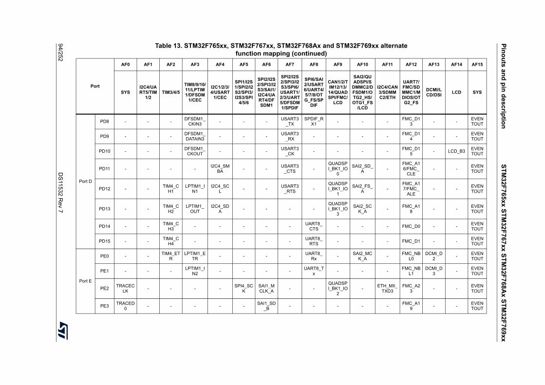
Pin
ou
ts a
nd
pin
de
scrip
tion
ST
M32
F76
5xx
ST
M32
F76
7xx
ST
M3
2F7
68A
x S
TM
32F
769x
x
94/2
52D
S115
32 Rev 7
Port D
PD8 - - -DFSDM1_
CKIN3- - -
USART3_TX
SPDIF_RX1
- - -FMC_D1
3- -
EVENTOUT
PD9 - - -DFSDM1_DATAIN3
- - -USART3
_RX- - - -
FMC_D14
- -EVENTOUT
PD10 - - -DFSDM1_
CKOUT- - -
USART3_CK
- - - -FMC_D1
5- LCD_B3
EVENTOUT
PD11 - - - -I2C4_SM
BA- -
USART3_CTS
-QUADSPI_BK1_IO
0
SAI2_SD_A
-FMC_A16/FMC_
CLE- -
EVENTOUT
PD12 - -TIM4_C
H1LPTIM1_I
N1I2C4_SC
L- -
USART3_RTS
-QUADSPI_BK1_IO
1
SAI2_FS_A
-FMC_A17/FMC_
ALE- -
EVENTOUT
PD13 - -TIM4_C
H2LPTIM1_
OUTI2C4_SD
A- - - -
QUADSPI_BK1_IO
3
SAI2_SCK_A
-FMC_A1
8- -
EVENTOUT
PD14 - -TIM4_C
H3- - - - -
UART8_CTS
- - - FMC_D0 - -EVENTOUT
PD15 - -TIM4_C
H4- - - - -
UART8_RTS
- - - FMC_D1 - -EVENTOUT
Port E
PE0 - -TIM4_ET
RLPTIM1_E
TR- - - -
UART8_Rx
-SAI2_MC
K_A-
FMC_NBL0
DCMI_D2
-EVENTOUT
PE1 - - -LPTIM1_I
N2- - - -
UART8_Tx
- - -FMC_NB
L1DCMI_D
3-
EVENTOUT
PE2TRACEC
LK- - - -
SPI4_SCK
SAI1_MCLK_A
- -QUADSPI_BK1_IO
2-
ETH_MII_TXD3
FMC_A23
- -EVENTOUT
PE3TRACED
0- - - - -
SAI1_SD_B
- - - - -FMC_A1
9- -
EVENTOUT
Table 13. STM32F765xx, STM32F767xx, STM32F768Ax and STM32F769xx alternatefunction mapping (continued)
Port
AF0 AF1 AF2 AF3 AF4 AF5 AF6 AF7 AF8 AF9 AF10 AF11 AF12 AF13 AF14 AF15
SYSI2C4/UART5/TIM
1/2TIM3/4/5
TIM8/9/10/11/LPTIM1/DFSDM
1/CEC
I2C1/2/3/4/USART
1/CEC
SPI1/I2S1/SPI2/I2S2/SPI3/I2S3/SPI
4/5/6
SPI2/I2S2/SPI3/I2S3/SAI1/I2C4/UART4/DFSDM1
SPI2/I2S2/SPI3/I2S3/SPI6/USART1/2/3/UART5/DFSDM1/SPDIF
SPI6/SAI2/USART6/UART4/5/7/8/OTG_FS/SP
DIF
CAN1/2/TIM12/13/14/QUADSPI/FMC/
LCD
SAI2/QUADSPI/S
DMMC2/DFSDM1/OTG2_HS/OTG1_FS
/LCD
I2C4/CAN3/SDMMC2/ETH
UART7/FMC/SDMMC1/MDIOS/OTG2_FS
DCMI/LCD/DSI
LCD SYS
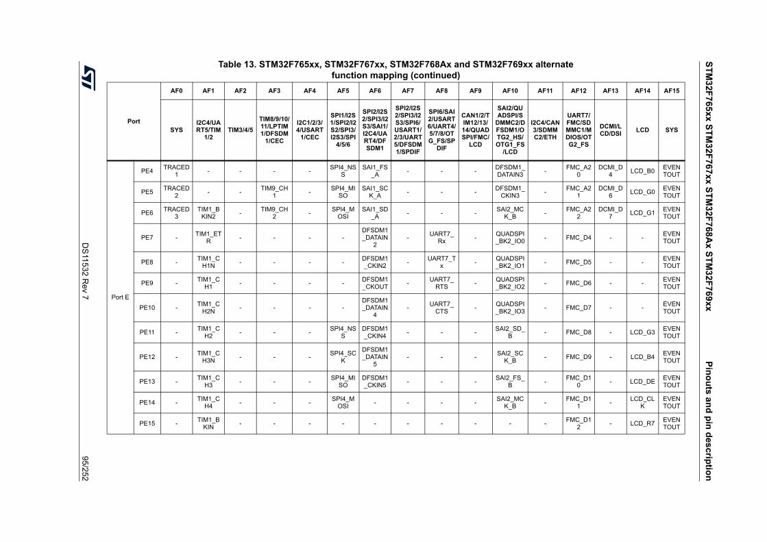
ST
M3
2F7
65xx
ST
M3
2F7
67xx
ST
M3
2F7
68A
x S
TM
32F
769
xxP
ino
uts
an
d p
in d
esc
riptio
n
DS
11532 R
ev 795/252
Port E
PE4TRACED
1- - - -
SPI4_NSS
SAI1_FS_A
- - -DFSDM1_DATAIN3
-FMC_A2
0DCMI_D
4LCD_B0
EVENTOUT
PE5TRACED
2- -
TIM9_CH1
-SPI4_MI
SOSAI1_SC
K_A- - -
DFSDM1_CKIN3
-FMC_A2
1DCMI_D
6LCD_G0
EVENTOUT
PE6TRACED
3TIM1_B
KIN2-
TIM9_CH2
-SPI4_M
OSISAI1_SD
_A- - -
SAI2_MCK_B
-FMC_A2
2DCMI_D
7LCD_G1
EVENTOUT
PE7 -TIM1_ET
R- - - -
DFSDM1_DATAIN
2-
UART7_Rx
-QUADSPI_BK2_IO0
- FMC_D4 - -EVENTOUT
PE8 -TIM1_C
H1N- - - -
DFSDM1_CKIN2
-UART7_T
x-
QUADSPI_BK2_IO1
- FMC_D5 - -EVENTOUT
PE9 -TIM1_C
H1- - - -
DFSDM1_CKOUT
-UART7_
RTS-
QUADSPI_BK2_IO2
- FMC_D6 - -EVENTOUT
PE10 -TIM1_C
H2N- - - -
DFSDM1_DATAIN
4-
UART7_CTS
-QUADSPI_BK2_IO3
- FMC_D7 - -EVENTOUT
PE11 -TIM1_C
H2- - -
SPI4_NSS
DFSDM1_CKIN4
- - -SAI2_SD_
B- FMC_D8 - LCD_G3
EVENTOUT
PE12 -TIM1_C
H3N- - -
SPI4_SCK
DFSDM1_DATAIN
5- - -
SAI2_SCK_B
- FMC_D9 - LCD_B4EVENTOUT
PE13 -TIM1_C
H3- - -
SPI4_MISO
DFSDM1_CKIN5
- - -SAI2_FS_
B-
FMC_D10
- LCD_DEEVENTOUT
PE14 -TIM1_C
H4- - -
SPI4_MOSI
- - - -SAI2_MC
K_B-
FMC_D11
-LCD_CL
KEVENTOUT
PE15 -TIM1_B
KIN- - - - - - - - - -
FMC_D12
- LCD_R7EVENTOUT
Table 13. STM32F765xx, STM32F767xx, STM32F768Ax and STM32F769xx alternatefunction mapping (continued)
Port
AF0 AF1 AF2 AF3 AF4 AF5 AF6 AF7 AF8 AF9 AF10 AF11 AF12 AF13 AF14 AF15
SYSI2C4/UART5/TIM
1/2TIM3/4/5
TIM8/9/10/11/LPTIM1/DFSDM
1/CEC
I2C1/2/3/4/USART
1/CEC
SPI1/I2S1/SPI2/I2S2/SPI3/I2S3/SPI
4/5/6
SPI2/I2S2/SPI3/I2S3/SAI1/I2C4/UART4/DFSDM1
SPI2/I2S2/SPI3/I2S3/SPI6/USART1/2/3/UART5/DFSDM1/SPDIF
SPI6/SAI2/USART6/UART4/5/7/8/OTG_FS/SP
DIF
CAN1/2/TIM12/13/14/QUADSPI/FMC/
LCD
SAI2/QUADSPI/S
DMMC2/DFSDM1/OTG2_HS/OTG1_FS
/LCD
I2C4/CAN3/SDMMC2/ETH
UART7/FMC/SDMMC1/MDIOS/OTG2_FS
DCMI/LCD/DSI
LCD SYS
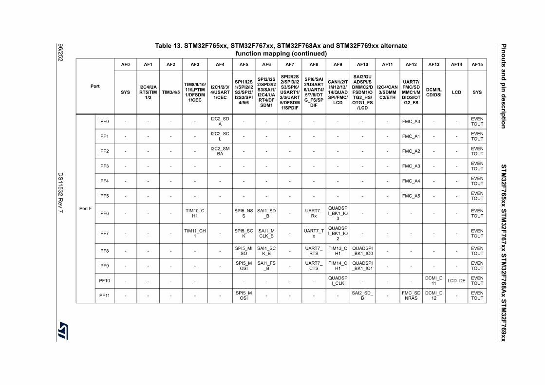
Pin
ou
ts a
nd
pin
de
scrip
tion
ST
M32
F76
5xx
ST
M32
F76
7xx
ST
M3
2F7
68A
x S
TM
32F
769x
x
96/2
52D
S115
32 Rev 7 Port F
PF0 - - - -I2C2_SD
A- - - - - - - FMC_A0 - -
EVENTOUT
PF1 - - - -I2C2_SC
L- - - - - - - FMC_A1 - -
EVENTOUT
PF2 - - - -I2C2_SM
BA- - - - - - - FMC_A2 - -
EVENTOUT
PF3 - - - - - - - - - - - - FMC_A3 - -EVENTOUT
PF4 - - - - - - - - - - - - FMC_A4 - -EVENTOUT
PF5 - - - - - - - - - - - - FMC_A5 - -EVENTOUT
PF6 - - -TIM10_C
H1-
SPI5_NSS
SAI1_SD_B
-UART7_
Rx
QUADSPI_BK1_IO
3- - - - -
EVENTOUT
PF7 - - -TIM11_CH
1-
SPI5_SCK
SAI1_MCLK_B
-UART7_T
x
QUADSPI_BK1_IO
2- - - - -
EVENTOUT
PF8 - - - - -SPI5_MI
SOSAI1_SC
K_B-
UART7_RTS
TIM13_CH1
QUADSPI_BK1_IO0
- - - -EVENTOUT
PF9 - - - - -SPI5_M
OSISAI1_FS
_B-
UART7_CTS
TIM14_CH1
QUADSPI_BK1_IO1
- - - -EVENTOUT
PF10 - - - - - - - - -QUADSP
I_CLK- - -
DCMI_D11
LCD_DEEVENTOUT
PF11 - - - - -SPI5_M
OSI- - - -
SAI2_SD_B
-FMC_SD
NRASDCMI_D
12-
EVENTOUT
Table 13. STM32F765xx, STM32F767xx, STM32F768Ax and STM32F769xx alternatefunction mapping (continued)
Port
AF0 AF1 AF2 AF3 AF4 AF5 AF6 AF7 AF8 AF9 AF10 AF11 AF12 AF13 AF14 AF15
SYSI2C4/UART5/TIM
1/2TIM3/4/5
TIM8/9/10/11/LPTIM1/DFSDM
1/CEC
I2C1/2/3/4/USART
1/CEC
SPI1/I2S1/SPI2/I2S2/SPI3/I2S3/SPI
4/5/6
SPI2/I2S2/SPI3/I2S3/SAI1/I2C4/UART4/DFSDM1
SPI2/I2S2/SPI3/I2S3/SPI6/USART1/2/3/UART5/DFSDM1/SPDIF
SPI6/SAI2/USART6/UART4/5/7/8/OTG_FS/SP
DIF
CAN1/2/TIM12/13/14/QUADSPI/FMC/
LCD
SAI2/QUADSPI/S
DMMC2/DFSDM1/OTG2_HS/OTG1_FS
/LCD
I2C4/CAN3/SDMMC2/ETH
UART7/FMC/SDMMC1/MDIOS/OTG2_FS
DCMI/LCD/DSI
LCD SYS
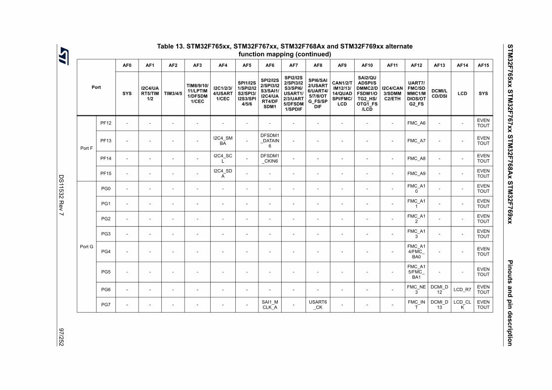
ST
M3
2F7
65xx
ST
M3
2F7
67xx
ST
M3
2F7
68A
x S
TM
32F
769
xxP
ino
uts
an
d p
in d
esc
riptio
n
DS
11532 R
ev 797/252
Port F
PF12 - - - - - - - - - - - - FMC_A6 - -EVENTOUT
PF13 - - - -I2C4_SM
BA-
DFSDM1_DATAIN
6- - - - - FMC_A7 - -
EVENTOUT
PF14 - - - -I2C4_SC
L-
DFSDM1_CKIN6
- - - - - FMC_A8 - -EVENTOUT
PF15 - - - -I2C4_SD
A- - - - - - - FMC_A9 - -
EVENTOUT
Port G
PG0 - - - - - - - - - - - -FMC_A1
0- -
EVENTOUT
PG1 - - - - - - - - - - - -FMC_A1
1- -
EVENTOUT
PG2 - - - - - - - - - - - -FMC_A1
2- -
EVENTOUT
PG3 - - - - - - - - - - - -FMC_A1
3- -
EVENTOUT
PG4 - - - - - - - - - - - -FMC_A14/FMC_
BA0- -
EVENTOUT
PG5 - - - - - - - - - - - -FMC_A15/FMC_
BA1- -
EVENTOUT
PG6 - - - - - - - - - - - -FMC_NE
3DCMI_D
12LCD_R7
EVENTOUT
PG7 - - - - - -SAI1_MCLK_A
-USART6
_CK- - -
FMC_INT
DCMI_D13
LCD_CLK
EVENTOUT
Table 13. STM32F765xx, STM32F767xx, STM32F768Ax and STM32F769xx alternatefunction mapping (continued)
Port
AF0 AF1 AF2 AF3 AF4 AF5 AF6 AF7 AF8 AF9 AF10 AF11 AF12 AF13 AF14 AF15
SYSI2C4/UART5/TIM
1/2TIM3/4/5
TIM8/9/10/11/LPTIM1/DFSDM
1/CEC
I2C1/2/3/4/USART
1/CEC
SPI1/I2S1/SPI2/I2S2/SPI3/I2S3/SPI
4/5/6
SPI2/I2S2/SPI3/I2S3/SAI1/I2C4/UART4/DFSDM1
SPI2/I2S2/SPI3/I2S3/SPI6/USART1/2/3/UART5/DFSDM1/SPDIF
SPI6/SAI2/USART6/UART4/5/7/8/OTG_FS/SP
DIF
CAN1/2/TIM12/13/14/QUADSPI/FMC/
LCD
SAI2/QUADSPI/S
DMMC2/DFSDM1/OTG2_HS/OTG1_FS
/LCD
I2C4/CAN3/SDMMC2/ETH
UART7/FMC/SDMMC1/MDIOS/OTG2_FS
DCMI/LCD/DSI
LCD SYS
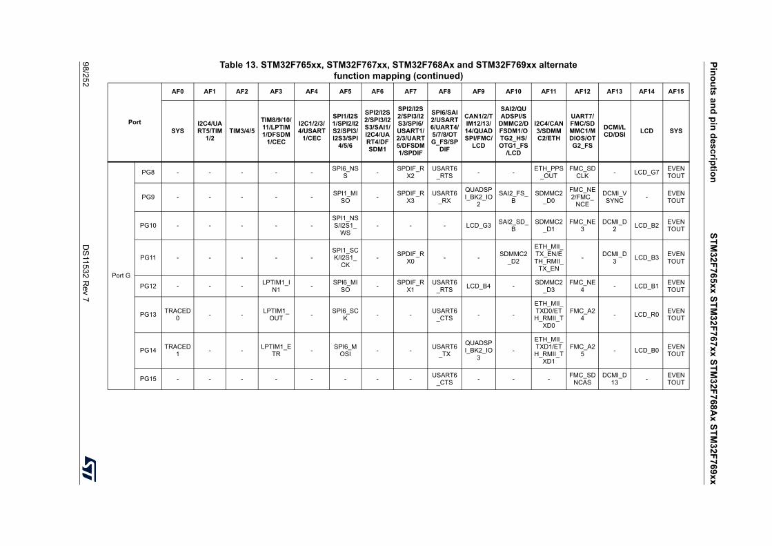
Pin
ou
ts a
nd
pin
de
scrip
tion
ST
M32
F76
5xx
ST
M32
F76
7xx
ST
M3
2F7
68A
x S
TM
32F
769x
x
98/2
52D
S115
32 Rev 7
Port G
PG8 - - - - -SPI6_NS
S-
SPDIF_RX2
USART6_RTS
- -ETH_PPS
_OUTFMC_SD
CLK- LCD_G7
EVENTOUT
PG9 - - - - -SPI1_MI
SO-
SPDIF_RX3
USART6_RX
QUADSPI_BK2_IO
2
SAI2_FS_B
SDMMC2_D0
FMC_NE2/FMC_
NCE
DCMI_VSYNC
-EVENTOUT
PG10 - - - - -SPI1_NSS/I2S1_
WS- - - LCD_G3
SAI2_SD_B
SDMMC2_D1
FMC_NE3
DCMI_D2
LCD_B2EVENTOUT
PG11 - - - - -SPI1_SCK/I2S1_
CK-
SPDIF_RX0
- -SDMMC2
_D2
ETH_MII_TX_EN/ETH_RMII_
TX_EN
-DCMI_D
3LCD_B3
EVENTOUT
PG12 - - -LPTIM1_I
N1-
SPI6_MISO
-SPDIF_R
X1USART6
_RTSLCD_B4 -
SDMMC2_D3
FMC_NE4
- LCD_B1EVENTOUT
PG13TRACED
0- -
LPTIM1_OUT
-SPI6_SC
K- -
USART6_CTS
- -
ETH_MII_TXD0/ETH_RMII_T
XD0
FMC_A24
- LCD_R0EVENTOUT
PG14TRACED
1- -
LPTIM1_ETR
-SPI6_M
OSI- -
USART6_TX
QUADSPI_BK2_IO
3-
ETH_MII_TXD1/ETH_RMII_T
XD1
FMC_A25
- LCD_B0EVENTOUT
PG15 - - - - - - - -USART6
_CTS- - -
FMC_SDNCAS
DCMI_D13
-EVENTOUT
Table 13. STM32F765xx, STM32F767xx, STM32F768Ax and STM32F769xx alternatefunction mapping (continued)
Port
AF0 AF1 AF2 AF3 AF4 AF5 AF6 AF7 AF8 AF9 AF10 AF11 AF12 AF13 AF14 AF15
SYSI2C4/UART5/TIM
1/2TIM3/4/5
TIM8/9/10/11/LPTIM1/DFSDM
1/CEC
I2C1/2/3/4/USART
1/CEC
SPI1/I2S1/SPI2/I2S2/SPI3/I2S3/SPI
4/5/6
SPI2/I2S2/SPI3/I2S3/SAI1/I2C4/UART4/DFSDM1
SPI2/I2S2/SPI3/I2S3/SPI6/USART1/2/3/UART5/DFSDM1/SPDIF
SPI6/SAI2/USART6/UART4/5/7/8/OTG_FS/SP
DIF
CAN1/2/TIM12/13/14/QUADSPI/FMC/
LCD
SAI2/QUADSPI/S
DMMC2/DFSDM1/OTG2_HS/OTG1_FS
/LCD
I2C4/CAN3/SDMMC2/ETH
UART7/FMC/SDMMC1/MDIOS/OTG2_FS
DCMI/LCD/DSI
LCD SYS
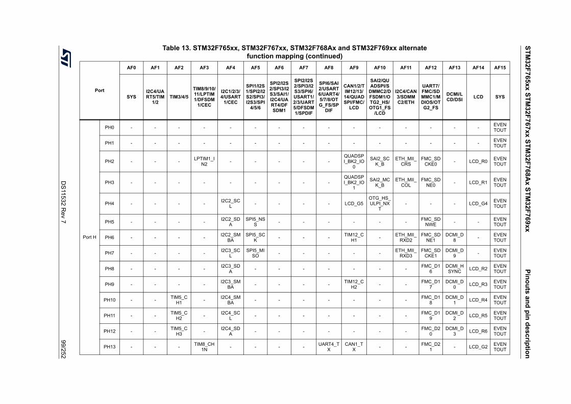
ST
M3
2F7
65xx
ST
M3
2F7
67xx
ST
M3
2F7
68A
x S
TM
32F
769
xxP
ino
uts
an
d p
in d
esc
riptio
n
DS
11532 R
ev 799/252
Port H
PH0 - - - - - - - - - - - - - - -EVENTOUT
PH1 - - - - - - - - - - - - - - -EVENTOUT
PH2 - - -LPTIM1_I
N2- - - - -
QUADSPI_BK2_IO
0
SAI2_SCK_B
ETH_MII_CRS
FMC_SDCKE0
- LCD_R0EVENTOUT
PH3 - - - - - - - - -QUADSPI_BK2_IO
1
SAI2_MCK_B
ETH_MII_COL
FMC_SDNE0
- LCD_R1EVENTOUT
PH4 - - - -I2C2_SC
L- - - - LCD_G5
OTG_HS_ULPI_NX
T- - - LCD_G4
EVENTOUT
PH5 - - - -I2C2_SD
ASPI5_NS
S- - - - - -
FMC_SDNWE
- -EVENTOUT
PH6 - - - -I2C2_SM
BASPI5_SC
K- - -
TIM12_CH1
-ETH_MII_
RXD2FMC_SD
NE1DCMI_D
8-
EVENTOUT
PH7 - - - -I2C3_SC
LSPI5_MI
SO- - - - -
ETH_MII_RXD3
FMC_SDCKE1
DCMI_D9
-EVENTOUT
PH8 - - - -I2C3_SD
A- - - - - - -
FMC_D16
DCMI_HSYNC
LCD_R2EVENTOUT
PH9 - - - -I2C3_SM
BA- - - -
TIM12_CH2
- -FMC_D1
7DCMI_D
0LCD_R3
EVENTOUT
PH10 - -TIM5_C
H1-
I2C4_SMBA
- - - - - - -FMC_D1
8DCMI_D
1LCD_R4
EVENTOUT
PH11 - -TIM5_C
H2-
I2C4_SCL
- - - - - - -FMC_D1
9DCMI_D
2LCD_R5
EVENTOUT
PH12 - -TIM5_C
H3-
I2C4_SDA
- - - - - - -FMC_D2
0DCMI_D
3LCD_R6
EVENTOUT
PH13 - - -TIM8_CH
1N- - - -
UART4_TX
CAN1_TX
- -FMC_D2
1- LCD_G2
EVENTOUT
Table 13. STM32F765xx, STM32F767xx, STM32F768Ax and STM32F769xx alternatefunction mapping (continued)
Port
AF0 AF1 AF2 AF3 AF4 AF5 AF6 AF7 AF8 AF9 AF10 AF11 AF12 AF13 AF14 AF15
SYSI2C4/UART5/TIM
1/2TIM3/4/5
TIM8/9/10/11/LPTIM1/DFSDM
1/CEC
I2C1/2/3/4/USART
1/CEC
SPI1/I2S1/SPI2/I2S2/SPI3/I2S3/SPI
4/5/6
SPI2/I2S2/SPI3/I2S3/SAI1/I2C4/UART4/DFSDM1
SPI2/I2S2/SPI3/I2S3/SPI6/USART1/2/3/UART5/DFSDM1/SPDIF
SPI6/SAI2/USART6/UART4/5/7/8/OTG_FS/SP
DIF
CAN1/2/TIM12/13/14/QUADSPI/FMC/
LCD
SAI2/QUADSPI/S
DMMC2/DFSDM1/OTG2_HS/OTG1_FS
/LCD
I2C4/CAN3/SDMMC2/ETH
UART7/FMC/SDMMC1/MDIOS/OTG2_FS
DCMI/LCD/DSI
LCD SYS
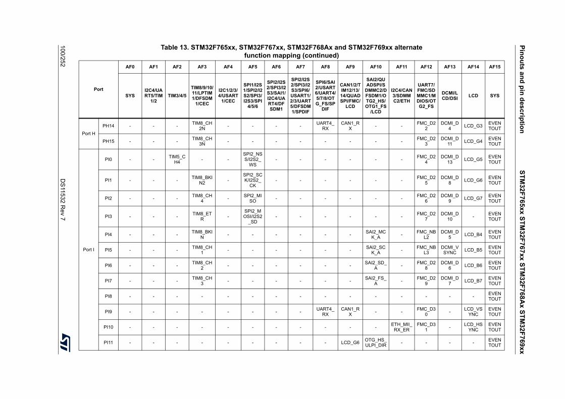
Pin
ou
ts a
nd
pin
de
scrip
tion
ST
M32
F76
5xx
ST
M32
F76
7xx
ST
M3
2F7
68A
x S
TM
32F
769x
x
100/252
DS
11532 R
ev 7
Port H
PH14 - - -TIM8_CH
2N- - - -
UART4_RX
CAN1_RX
- -FMC_D2
2DCMI_D
4LCD_G3
EVENTOUT
PH15 - - -TIM8_CH
3N- - - - - - - -
FMC_D23
DCMI_D11
LCD_G4EVENTOUT
Port I
PI0 - -TIM5_C
H4- -
SPI2_NSS/I2S2_
WS- - - - - -
FMC_D24
DCMI_D13
LCD_G5EVENTOUT
PI1 - - -TIM8_BKI
N2-
SPI2_SCK/I2S2_
CK- - - - - -
FMC_D25
DCMI_D8
LCD_G6EVENTOUT
PI2 - - -TIM8_CH
4-
SPI2_MISO
- - - - - -FMC_D2
6DCMI_D
9LCD_G7
EVENTOUT
PI3 - - -TIM8_ET
R-
SPI2_MOSI/I2S2
_SD- - - - - -
FMC_D27
DCMI_D10
-EVENTOUT
PI4 - - -TIM8_BKI
N- - - - - -
SAI2_MCK_A
-FMC_NB
L2DCMI_D
5LCD_B4
EVENTOUT
PI5 - - -TIM8_CH
1- - - - - -
SAI2_SCK_A
-FMC_NB
L3DCMI_VSYNC
LCD_B5EVENTOUT
PI6 - - -TIM8_CH
2- - - - - -
SAI2_SD_A
-FMC_D2
8DCMI_D
6LCD_B6
EVENTOUT
PI7 - - -TIM8_CH
3- - - - - -
SAI2_FS_A
-FMC_D2
9DCMI_D
7LCD_B7
EVENTOUT
PI8 - - - - - - - - - - - - - - -EVENTOUT
PI9 - - - - - - - -UART4_
RXCAN1_R
X- -
FMC_D30
-LCD_VS
YNCEVENTOUT
PI10 - - - - - - - - - - -ETH_MII_
RX_ERFMC_D3
1-
LCD_HSYNC
EVENTOUT
PI11 - - - - - - - - - LCD_G6OTG_HS_ULPI_DIR
- - - -EVENTOUT
Table 13. STM32F765xx, STM32F767xx, STM32F768Ax and STM32F769xx alternatefunction mapping (continued)
Port
AF0 AF1 AF2 AF3 AF4 AF5 AF6 AF7 AF8 AF9 AF10 AF11 AF12 AF13 AF14 AF15
SYSI2C4/UART5/TIM
1/2TIM3/4/5
TIM8/9/10/11/LPTIM1/DFSDM
1/CEC
I2C1/2/3/4/USART
1/CEC
SPI1/I2S1/SPI2/I2S2/SPI3/I2S3/SPI
4/5/6
SPI2/I2S2/SPI3/I2S3/SAI1/I2C4/UART4/DFSDM1
SPI2/I2S2/SPI3/I2S3/SPI6/USART1/2/3/UART5/DFSDM1/SPDIF
SPI6/SAI2/USART6/UART4/5/7/8/OTG_FS/SP
DIF
CAN1/2/TIM12/13/14/QUADSPI/FMC/
LCD
SAI2/QUADSPI/S
DMMC2/DFSDM1/OTG2_HS/OTG1_FS
/LCD
I2C4/CAN3/SDMMC2/ETH
UART7/FMC/SDMMC1/MDIOS/OTG2_FS
DCMI/LCD/DSI
LCD SYS
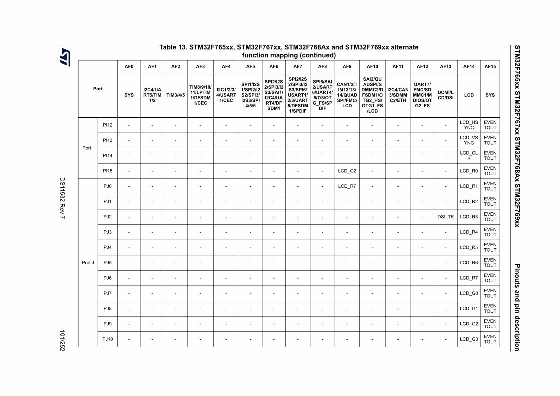
ST
M3
2F7
65xx
ST
M3
2F7
67xx
ST
M3
2F7
68A
x S
TM
32F
769
xxP
ino
uts
an
d p
in d
esc
riptio
n
DS
11532 R
ev 71
01/252
Port I
PI12 - - - - - - - - - - - - - -LCD_HS
YNCEVENTOUT
PI13 - - - - - - - - - - - - - -LCD_VS
YNCEVENTOUT
PI14 - - - - - - - - - - - - - -LCD_CL
KEVENTOUT
PI15 - - - - - - - - - LCD_G2 - - - - LCD_R0EVENTOUT
Port J
PJ0 - - - - - - - - - LCD_R7 - - - - LCD_R1EVENTOUT
PJ1 - - - - - - - - - - - - - - LCD_R2EVENTOUT
PJ2 - - - - - - - - - - - - - DSI_TE LCD_R3EVENTOUT
PJ3 - - - - - - - - - - - - - - LCD_R4EVENTOUT
PJ4 - - - - - - - - - - - - - - LCD_R5EVENTOUT
PJ5 - - - - - - - - - - - - - - LCD_R6EVENTOUT
PJ6 - - - - - - - - - - - - - - LCD_R7EVENTOUT
PJ7 - - - - - - - - - - - - - - LCD_G0EVENTOUT
PJ8 - - - - - - - - - - - - - - LCD_G1EVENTOUT
PJ9 - - - - - - - - - - - - - - LCD_G2EVENTOUT
PJ10 - - - - - - - - - - - - - - LCD_G3EVENTOUT
Table 13. STM32F765xx, STM32F767xx, STM32F768Ax and STM32F769xx alternatefunction mapping (continued)
Port
AF0 AF1 AF2 AF3 AF4 AF5 AF6 AF7 AF8 AF9 AF10 AF11 AF12 AF13 AF14 AF15
SYSI2C4/UART5/TIM
1/2TIM3/4/5
TIM8/9/10/11/LPTIM1/DFSDM
1/CEC
I2C1/2/3/4/USART
1/CEC
SPI1/I2S1/SPI2/I2S2/SPI3/I2S3/SPI
4/5/6
SPI2/I2S2/SPI3/I2S3/SAI1/I2C4/UART4/DFSDM1
SPI2/I2S2/SPI3/I2S3/SPI6/USART1/2/3/UART5/DFSDM1/SPDIF
SPI6/SAI2/USART6/UART4/5/7/8/OTG_FS/SP
DIF
CAN1/2/TIM12/13/14/QUADSPI/FMC/
LCD
SAI2/QUADSPI/S
DMMC2/DFSDM1/OTG2_HS/OTG1_FS
/LCD
I2C4/CAN3/SDMMC2/ETH
UART7/FMC/SDMMC1/MDIOS/OTG2_FS
DCMI/LCD/DSI
LCD SYS
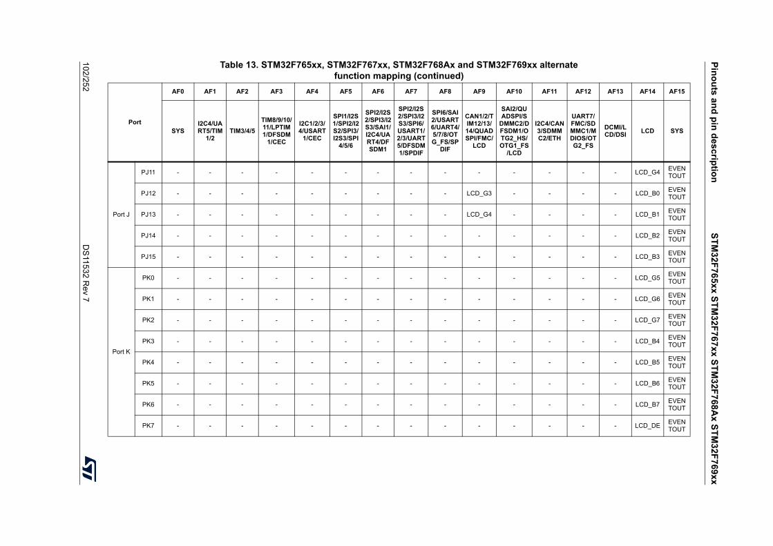
Pin
ou
ts a
nd
pin
de
scrip
tion
ST
M32
F76
5xx
ST
M32
F76
7xx
ST
M3
2F7
68A
x S
TM
32F
769x
x
102/252
DS
11532 R
ev 7
Port J
PJ11 - - - - - - - - - - - - - - LCD_G4EVENTOUT
PJ12 - - - - - - - - - LCD_G3 - - - - LCD_B0EVENTOUT
PJ13 - - - - - - - - - LCD_G4 - - - - LCD_B1EVENTOUT
PJ14 - - - - - - - - - - - - - - LCD_B2EVENTOUT
PJ15 - - - - - - - - - - - - - - LCD_B3EVENTOUT
Port K
PK0 - - - - - - - - - - - - - - LCD_G5EVENTOUT
PK1 - - - - - - - - - - - - - - LCD_G6EVENTOUT
PK2 - - - - - - - - - - - - - - LCD_G7EVENTOUT
PK3 - - - - - - - - - - - - - - LCD_B4EVENTOUT
PK4 - - - - - - - - - - - - - - LCD_B5EVENTOUT
PK5 - - - - - - - - - - - - - - LCD_B6EVENTOUT
PK6 - - - - - - - - - - - - - - LCD_B7EVENTOUT
PK7 - - - - - - - - - - - - - - LCD_DEEVENTOUT
Table 13. STM32F765xx, STM32F767xx, STM32F768Ax and STM32F769xx alternatefunction mapping (continued)
Port
AF0 AF1 AF2 AF3 AF4 AF5 AF6 AF7 AF8 AF9 AF10 AF11 AF12 AF13 AF14 AF15
SYSI2C4/UART5/TIM
1/2TIM3/4/5
TIM8/9/10/11/LPTIM1/DFSDM
1/CEC
I2C1/2/3/4/USART
1/CEC
SPI1/I2S1/SPI2/I2S2/SPI3/I2S3/SPI
4/5/6
SPI2/I2S2/SPI3/I2S3/SAI1/I2C4/UART4/DFSDM1
SPI2/I2S2/SPI3/I2S3/SPI6/USART1/2/3/UART5/DFSDM1/SPDIF
SPI6/SAI2/USART6/UART4/5/7/8/OTG_FS/SP
DIF
CAN1/2/TIM12/13/14/QUADSPI/FMC/
LCD
SAI2/QUADSPI/S
DMMC2/DFSDM1/OTG2_HS/OTG1_FS
/LCD
I2C4/CAN3/SDMMC2/ETH
UART7/FMC/SDMMC1/MDIOS/OTG2_FS
DCMI/LCD/DSI
LCD SYS
DS11532 Rev 7 103/252
STM32F765xx STM32F767xx STM32F768Ax STM32F769xx Memory mapping
103
5 Memory mapping
Refer to the product line reference manual for details on the memory mapping as well as the boundary addresses for all peripherals.
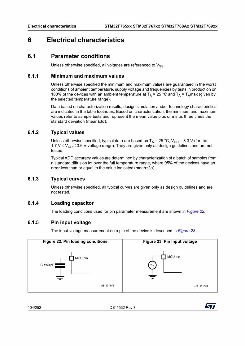
Electrical characteristics STM32F765xx STM32F767xx STM32F768Ax STM32F769xx
104/252 DS11532 Rev 7
6 Electrical characteristics
6.1 Parameter conditions
Unless otherwise specified, all voltages are referenced to VSS.
6.1.1 Minimum and maximum values
Unless otherwise specified the minimum and maximum values are guaranteed in the worst conditions of ambient temperature, supply voltage and frequencies by tests in production on 100% of the devices with an ambient temperature at TA = 25 °C and TA = TAmax (given by the selected temperature range).
Data based on characterization results, design simulation and/or technology characteristics are indicated in the table footnotes. Based on characterization, the minimum and maximum values refer to sample tests and represent the mean value plus or minus three times the standard deviation (mean±3σ).
6.1.2 Typical values
Unless otherwise specified, typical data are based on TA = 25 °C, VDD = 3.3 V (for the 1.7 V ≤ VDD ≤ 3.6 V voltage range). They are given only as design guidelines and are not tested.
Typical ADC accuracy values are determined by characterization of a batch of samples from a standard diffusion lot over the full temperature range, where 95% of the devices have an error less than or equal to the value indicated (mean±2σ).
6.1.3 Typical curves
Unless otherwise specified, all typical curves are given only as design guidelines and are not tested.
6.1.4 Loading capacitor
The loading conditions used for pin parameter measurement are shown in Figure 22.
6.1.5 Pin input voltage
The input voltage measurement on a pin of the device is described in Figure 23.
Figure 22. Pin loading conditions Figure 23. Pin input voltage
MS19011V2
C = 50 pF
MCU pin
MS19010V2
MCU pin
VIN

DS11532 Rev 7 105/252
STM32F765xx STM32F767xx STM32F768Ax STM32F769xx Electrical characteristics
218
6.1.6 Power supply scheme
Figure 24. STM32F769xx/STM32F779xx power supply scheme
MSv39619V1
Analog: RCs, PLL,
...
VBAT
Backup circuitry(OSC32K,RTC,
Backup registers,backup RAM)
Wakeup logicVBAT =
1.65 to 3.6V
VDDA
VREF+
VREF-
VSSA
ADC+ 1 μF
VREF
100 nF+ 1 μF
VDD
PDR_ONReset
controller
100 nF
2.2 μFDSI
PHY
DSI voltage regulator
VCAPDSI
VDD12DSI
VSSDSI
VDDDSI
VDD1/2/...14/20
Kernel logic (CPU, digital
& RAM)
20 × 100 nF+ 1 × 4.7 μF
Voltageregulator
VSS 1/2/...14/20
Leve
l shi
fter
VDD
Flash memory
CAP_1VCAP_22 × 2.2 μF
BYPASS_REG
OTG FS PHY100 nF
VDDUSB
+ 1 μF
VDDUSB
OUT
IN
IO
V
DDSDMMC
PG[9..12], PD[6,7]Logic
GP I/Os
OUT
IN
IOLogic
Leve
l shi
fter
V
Power switch
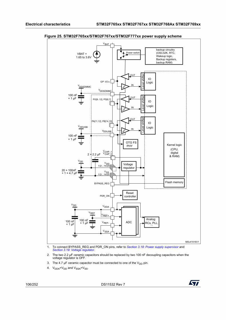
Electrical characteristics STM32F765xx STM32F767xx STM32F768Ax STM32F769xx
106/252 DS11532 Rev 7
Figure 25. STM32F765xx/STM32F767xx/STM32F777xx power supply scheme
1. To connect BYPASS_REG and PDR_ON pins, refer to Section 3.18: Power supply supervisor and Section 3.19: Voltage regulator.
2. The two 2.2 µF ceramic capacitors should be replaced by two 100 nF decoupling capacitors when the voltage regulator is OFF.
3. The 4.7 µF ceramic capacitor must be connected to one of the VDD pin.
4. VDDA=VDD and VSSA=VSS.
MSv41016V1
Analog:RCs, PLL,...
VDDA
VREF+
VREF-
VSSA
ADC+ 1 μF
VREF
100 nF+ 1 μF
VDD
PDR_ONReset
controller
100 nF
VDD1/2/...14/20
VBAT
Kernel logic (CPU, digital
& RAM)
backup circuitry (OSC32K, RTC, Wakeup logic, Backup registers, backup RAM)
20 × 100nF + 1 × 4.7 μF
VBAT =1.65 to 3.6V
Voltageregulator
VSS 1/2/...14/20
Leve
l shi
fter
VDD
Flash memory
CAP_1VCAP_22 × 2.2 μF
BYPASS_REG
OTG FS PHY
100 nF
VDDUSB
+ 1 μF
VDDUSB
OUT
IN
IO
V
DDSDMMC
PG[9..12], PD[6,7]
Logic
GP I/O s
OUT
IN
IOLogic
Leve
l shi
fter
V
Leve
l shi
fter
OUT
IN
IOPA[11,12], PB[14,15]
Logic
100 nF
VDDSDMMC
+ 1 μF
Power switch
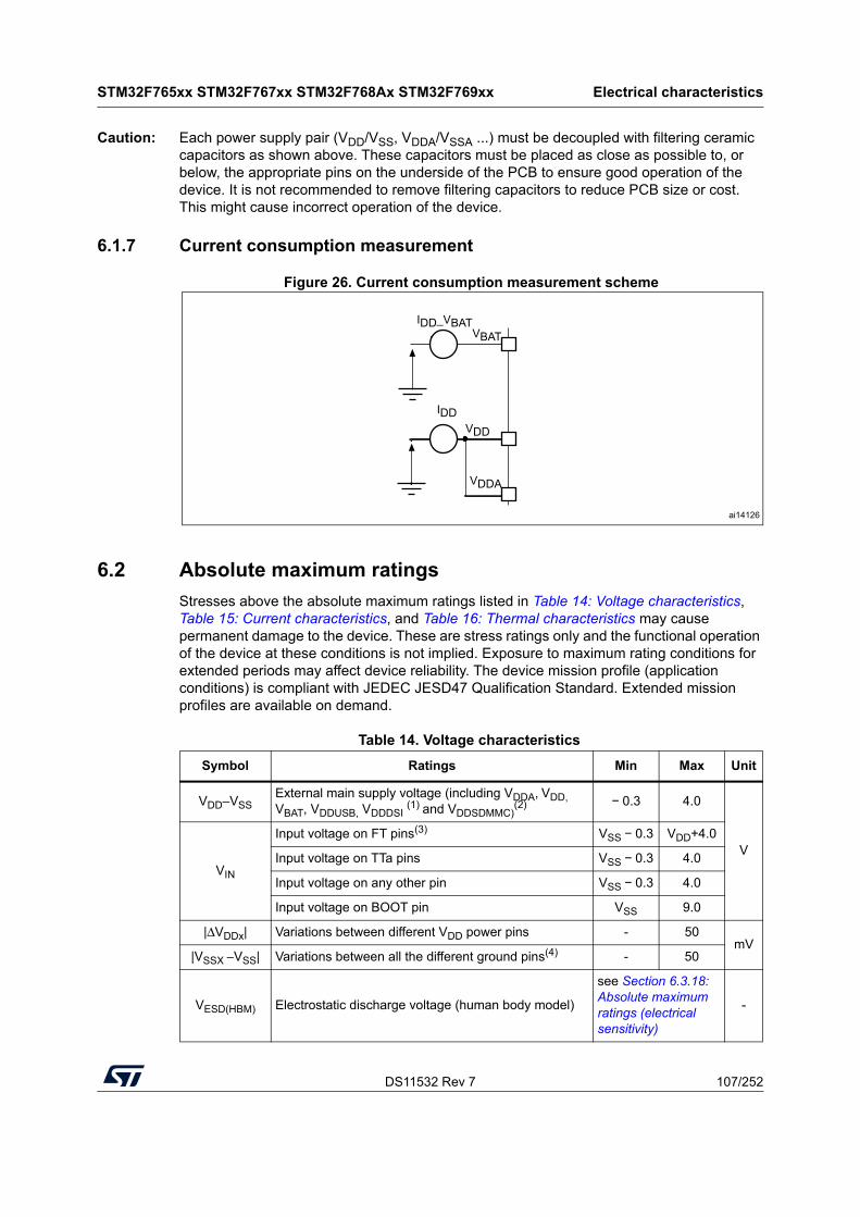
DS11532 Rev 7 107/252
STM32F765xx STM32F767xx STM32F768Ax STM32F769xx Electrical characteristics
218
Caution: Each power supply pair (VDD/VSS, VDDA/VSSA ...) must be decoupled with filtering ceramic capacitors as shown above. These capacitors must be placed as close as possible to, or below, the appropriate pins on the underside of the PCB to ensure good operation of the device. It is not recommended to remove filtering capacitors to reduce PCB size or cost. This might cause incorrect operation of the device.
6.1.7 Current consumption measurement
Figure 26. Current consumption measurement scheme
6.2 Absolute maximum ratings
Stresses above the absolute maximum ratings listed in Table 14: Voltage characteristics, Table 15: Current characteristics, and Table 16: Thermal characteristics may cause permanent damage to the device. These are stress ratings only and the functional operation of the device at these conditions is not implied. Exposure to maximum rating conditions for extended periods may affect device reliability. The device mission profile (application conditions) is compliant with JEDEC JESD47 Qualification Standard. Extended mission profiles are available on demand.
ai14126
VBAT
VDD
VDDA
IDD_VBAT
IDD
Table 14. Voltage characteristics
Symbol Ratings Min Max Unit
VDD–VSSExternal main supply voltage (including VDDA, VDD, VBAT, VDDUSB, VDDDSI
(1) and VDDSDMMC)(2) − 0.3 4.0
V
VIN
Input voltage on FT pins(3) VSS − 0.3 VDD+4.0
Input voltage on TTa pins VSS − 0.3 4.0
Input voltage on any other pin VSS − 0.3 4.0
Input voltage on BOOT pin VSS 9.0
|ΔVDDx| Variations between different VDD power pins - 50mV
|VSSX −VSS| Variations between all the different ground pins(4) - 50
VESD(HBM) Electrostatic discharge voltage (human body model)
see Section 6.3.18: Absolute maximum ratings (electrical sensitivity)
-
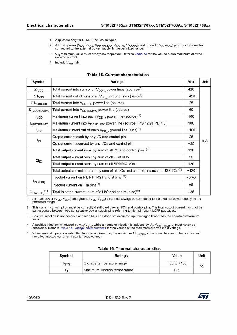
Electrical characteristics STM32F765xx STM32F767xx STM32F768Ax STM32F769xx
108/252 DS11532 Rev 7
1. Applicable only for STM32F7x9 sales types.
2. All main power (VDD, VDDA, VDDSDMMC, VDDUSB, VDDDSI) and ground (VSS, VSSA) pins must always be connected to the external power supply, in the permitted range.
3. VIN maximum value must always be respected. Refer to Table 15 for the values of the maximum allowed injected current.
4. Include VREF- pin.
Table 15. Current characteristics
Symbol Ratings Max. Unit
ΣIVDD Total current into sum of all VDD_x power lines (source)(1) 420
mA
Σ IVSS Total current out of sum of all VSS_x ground lines (sink)(1) −420
Σ IVDDUSB Total current into VDDUSB power line (source) 25
Σ IVDDSDMMC Total current into VDDSDMMC power line (source) 60
IVDD Maximum current into each VDD_x power line (source)(1) 100
IVDDSDMMC Maximum current into VDDSDMMC power line (source): PG[12:9], PD[7:6] 100
IVSS Maximum current out of each VSS_x ground line (sink)(1) −100
IIOOutput current sunk by any I/O and control pin 25
Output current sourced by any I/Os and control pin −25
ΣIIO
Total output current sunk by sum of all I/O and control pins (2) 120
Total output current sunk by sum of all USB I/Os 25
Total output current sunk by sum of all SDMMC I/Os 120
Total output current sourced by sum of all I/Os and control pins except USB I/Os(2) −120
IINJ(PIN)
Injected current on FT, FTf, RST and B pins (3) −5/+0
Injected current on TTa pins(4) ±5
ΣIINJ(PIN)(4) Total injected current (sum of all I/O and control pins)(5) ±25
1. All main power (VDD, VDDA) and ground (VSS, VSSA) pins must always be connected to the external power supply, in the permitted range.
2. This current consumption must be correctly distributed over all I/Os and control pins. The total output current must not be sunk/sourced between two consecutive power supply pins referring to high pin count LQFP packages.
3. Positive injection is not possible on these I/Os and does not occur for input voltages lower than the specified maximum value.
4. A positive injection is induced by VIN>VDDA while a negative injection is induced by VIN<VSS. IINJ(PIN) must never be exceeded. Refer to Table 14: Voltage characteristics for the values of the maximum allowed input voltage.
5. When several inputs are submitted to a current injection, the maximum ΣIINJ(PIN) is the absolute sum of the positive and negative injected currents (instantaneous values).
Table 16. Thermal characteristics
Symbol Ratings Value Unit
TSTG Storage temperature range − 65 to +150°C
TJ Maximum junction temperature 125
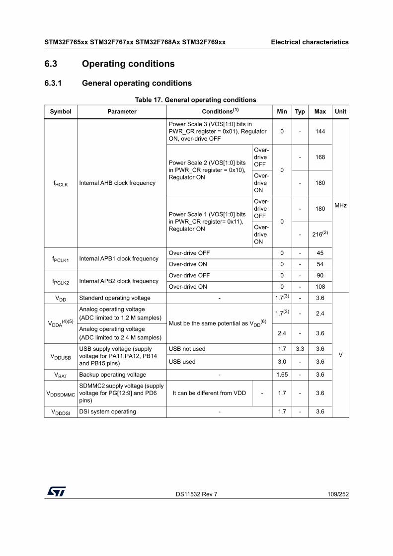
DS11532 Rev 7 109/252
STM32F765xx STM32F767xx STM32F768Ax STM32F769xx Electrical characteristics
218
6.3 Operating conditions
6.3.1 General operating conditions
Table 17. General operating conditions
Symbol Parameter Conditions(1) Min Typ Max Unit
fHCLK Internal AHB clock frequency
Power Scale 3 (VOS[1:0] bits in PWR_CR register = 0x01), Regulator ON, over-drive OFF
0 - 144
MHz
Power Scale 2 (VOS[1:0] bits in PWR_CR register = 0x10), Regulator ON
Over-drive OFF
0
- 168
Over-drive ON
- 180
Power Scale 1 (VOS[1:0] bits in PWR_CR register= 0x11), Regulator ON
Over-drive OFF
0
- 180
Over-drive ON
- 216(2)
fPCLK1 Internal APB1 clock frequencyOver-drive OFF 0 - 45
Over-drive ON 0 - 54
fPCLK2 Internal APB2 clock frequencyOver-drive OFF 0 - 90
Over-drive ON 0 - 108
VDD Standard operating voltage - 1.7(3) - 3.6
V
VDDA(4)(5)
Analog operating voltage
(ADC limited to 1.2 M samples)Must be the same potential as VDD
(6)
1.7(3) - 2.4
Analog operating voltage
(ADC limited to 2.4 M samples)2.4 - 3.6
VDDUSB
USB supply voltage (supply voltage for PA11,PA12, PB14 and PB15 pins)
USB not used 1.7 3.3 3.6
USB used 3.0 - 3.6
VBAT Backup operating voltage - 1.65 - 3.6
VDDSDMMC
SDMMC2 supply voltage (supply voltage for PG[12:9] and PD6 pins)
It can be different from VDD - 1.7 - 3.6
VDDDSI DSI system operating - 1.7 - 3.6
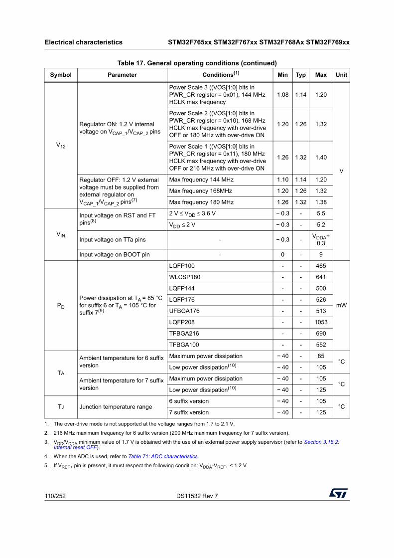
Electrical characteristics STM32F765xx STM32F767xx STM32F768Ax STM32F769xx
110/252 DS11532 Rev 7
V12
Regulator ON: 1.2 V internal voltage on VCAP_1/VCAP_2 pins
Power Scale 3 ((VOS[1:0] bits in PWR_CR register = 0x01), 144 MHz HCLK max frequency
1.08 1.14 1.20
V
Power Scale 2 ((VOS[1:0] bits in PWR_CR register = 0x10), 168 MHz HCLK max frequency with over-drive OFF or 180 MHz with over-drive ON
1.20 1.26 1.32
Power Scale 1 ((VOS[1:0] bits in PWR_CR register = 0x11), 180 MHz HCLK max frequency with over-drive OFF or 216 MHz with over-drive ON
1.26 1.32 1.40
Regulator OFF: 1.2 V external voltage must be supplied from external regulator on VCAP_1/VCAP_2 pins(7)
Max frequency 144 MHz 1.10 1.14 1.20
Max frequency 168MHz 1.20 1.26 1.32
Max frequency 180 MHz 1.26 1.32 1.38
VIN
Input voltage on RST and FT pins(8)
2 V ≤ VDD ≤ 3.6 V − 0.3 - 5.5
VDD ≤ 2 V − 0.3 - 5.2
Input voltage on TTa pins - − 0.3 -VDDA+
0.3
Input voltage on BOOT pin - 0 - 9
PD
Power dissipation at TA = 85 °C for suffix 6 or TA = 105 °C for suffix 7(9)
LQFP100 - - 465
mW
WLCSP180 - - 641
LQFP144 - - 500
LQFP176 - - 526
UFBGA176 - - 513
LQFP208 - - 1053
TFBGA216 - - 690
TFBGA100 - - 552
TA
Ambient temperature for 6 suffix version
Maximum power dissipation − 40 - 85°C
Low power dissipation(10) − 40 - 105
Ambient temperature for 7 suffix version
Maximum power dissipation − 40 - 105°C
Low power dissipation(10) − 40 - 125
TJ Junction temperature range6 suffix version − 40 - 105
°C7 suffix version − 40 - 125
1. The over-drive mode is not supported at the voltage ranges from 1.7 to 2.1 V.
2. 216 MHz maximum frequency for 6 suffix version (200 MHz maximum frequency for 7 suffix version).
3. VDD/VDDA minimum value of 1.7 V is obtained with the use of an external power supply supervisor (refer to Section 3.18.2: Internal reset OFF).
4. When the ADC is used, refer to Table 71: ADC characteristics.
5. If VREF+ pin is present, it must respect the following condition: VDDA-VREF+ < 1.2 V.
Table 17. General operating conditions (continued)
Symbol Parameter Conditions(1) Min Typ Max Unit
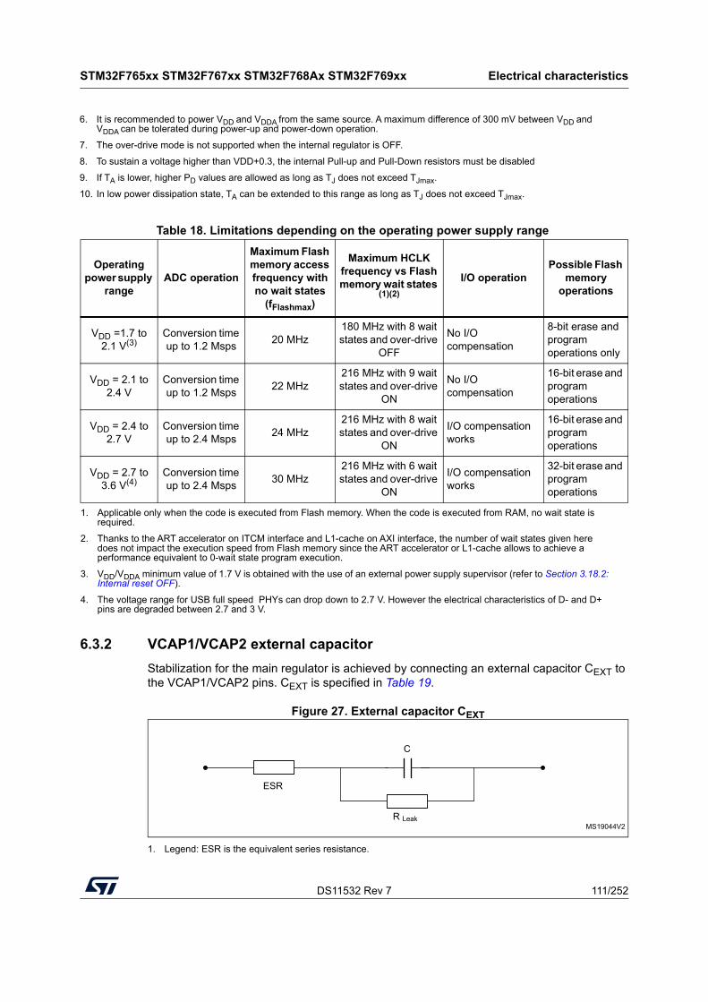
DS11532 Rev 7 111/252
STM32F765xx STM32F767xx STM32F768Ax STM32F769xx Electrical characteristics
218
6.3.2 VCAP1/VCAP2 external capacitor
Stabilization for the main regulator is achieved by connecting an external capacitor CEXT to the VCAP1/VCAP2 pins. CEXT is specified in Table 19.
Figure 27. External capacitor CEXT
1. Legend: ESR is the equivalent series resistance.
6. It is recommended to power VDD and VDDA from the same source. A maximum difference of 300 mV between VDD and VDDA can be tolerated during power-up and power-down operation.
7. The over-drive mode is not supported when the internal regulator is OFF.
8. To sustain a voltage higher than VDD+0.3, the internal Pull-up and Pull-Down resistors must be disabled
9. If TA is lower, higher PD values are allowed as long as TJ does not exceed TJmax.
10. In low power dissipation state, TA can be extended to this range as long as TJ does not exceed TJmax.
Table 18. Limitations depending on the operating power supply range
Operating power supply
rangeADC operation
Maximum Flash memory access frequency with no wait states
(fFlashmax)
Maximum HCLK frequency vs Flash memory wait states
(1)(2)
I/O operationPossible Flash
memory operations
VDD =1.7 to 2.1 V(3)
Conversion time up to 1.2 Msps
20 MHz180 MHz with 8 wait states and over-drive
OFF
No I/O compensation
8-bit erase and program operations only
VDD = 2.1 to 2.4 V
Conversion time up to 1.2 Msps
22 MHz216 MHz with 9 wait states and over-drive
ON
No I/O compensation
16-bit erase and program operations
VDD = 2.4 to 2.7 V
Conversion time up to 2.4 Msps
24 MHz 216 MHz with 8 wait states and over-drive
ON
I/O compensation works
16-bit erase and program operations
VDD = 2.7 to 3.6 V(4)
Conversion time up to 2.4 Msps
30 MHz216 MHz with 6 wait states and over-drive
ON
I/O compensation works
32-bit erase and program operations
1. Applicable only when the code is executed from Flash memory. When the code is executed from RAM, no wait state is required.
2. Thanks to the ART accelerator on ITCM interface and L1-cache on AXI interface, the number of wait states given here does not impact the execution speed from Flash memory since the ART accelerator or L1-cache allows to achieve a performance equivalent to 0-wait state program execution.
3. VDD/VDDA minimum value of 1.7 V is obtained with the use of an external power supply supervisor (refer to Section 3.18.2: Internal reset OFF).
4. The voltage range for USB full speed PHYs can drop down to 2.7 V. However the electrical characteristics of D- and D+ pins are degraded between 2.7 and 3 V.
MS19044V2
ESR
R Leak
C
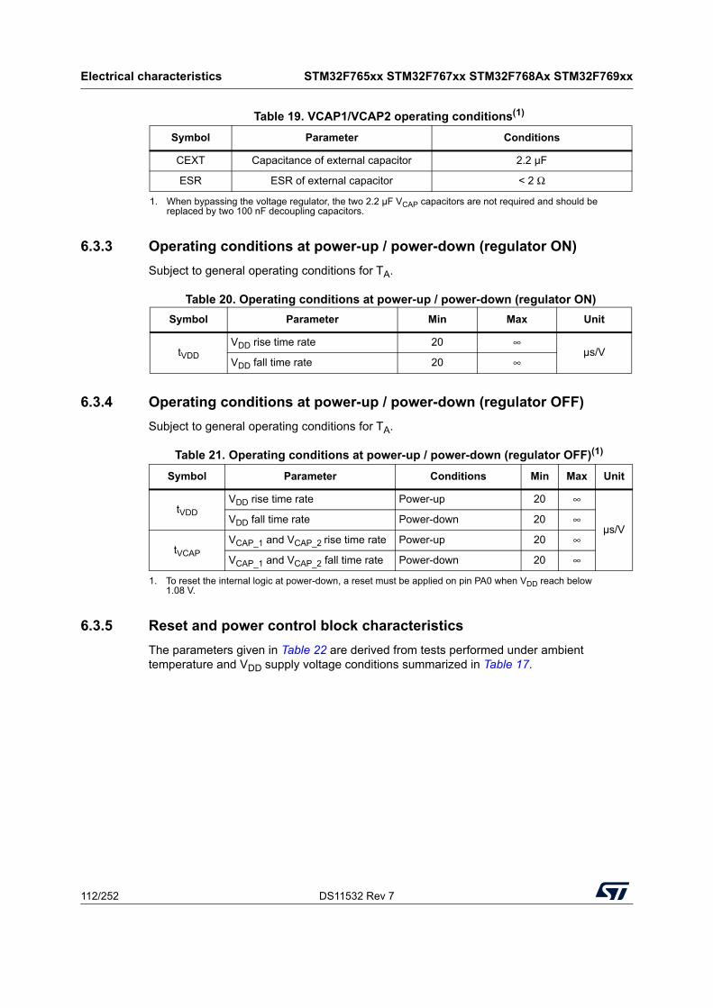
Electrical characteristics STM32F765xx STM32F767xx STM32F768Ax STM32F769xx
112/252 DS11532 Rev 7
6.3.3 Operating conditions at power-up / power-down (regulator ON)
Subject to general operating conditions for TA.
Table 20. Operating conditions at power-up / power-down (regulator ON)
6.3.4 Operating conditions at power-up / power-down (regulator OFF)
Subject to general operating conditions for TA.
6.3.5 Reset and power control block characteristics
The parameters given in Table 22 are derived from tests performed under ambient temperature and VDD supply voltage conditions summarized in Table 17.
Table 19. VCAP1/VCAP2 operating conditions(1)
1. When bypassing the voltage regulator, the two 2.2 µF VCAP capacitors are not required and should be replaced by two 100 nF decoupling capacitors.
Symbol Parameter Conditions
CEXT Capacitance of external capacitor 2.2 µF
ESR ESR of external capacitor < 2 Ω
Symbol Parameter Min Max Unit
tVDD
VDD rise time rate 20 ∞µs/V
VDD fall time rate 20 ∞
Table 21. Operating conditions at power-up / power-down (regulator OFF)(1)
1. To reset the internal logic at power-down, a reset must be applied on pin PA0 when VDD reach below 1.08 V.
Symbol Parameter Conditions Min Max Unit
tVDD
VDD rise time rate Power-up 20 ∞
µs/VVDD fall time rate Power-down 20 ∞
tVCAP
VCAP_1 and VCAP_2 rise time rate Power-up 20 ∞
VCAP_1 and VCAP_2 fall time rate Power-down 20 ∞
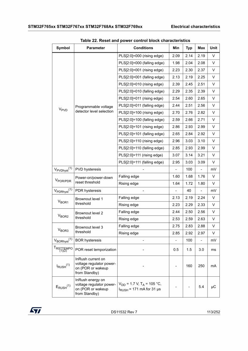
DS11532 Rev 7 113/252
STM32F765xx STM32F767xx STM32F768Ax STM32F769xx Electrical characteristics
218
Table 22. Reset and power control block characteristics
Symbol Parameter Conditions Min Typ Max Unit
VPVDProgrammable voltage detector level selection
PLS[2:0]=000 (rising edge) 2.09 2.14 2.19 V
PLS[2:0]=000 (falling edge) 1.98 2.04 2.08 V
PLS[2:0]=001 (rising edge) 2.23 2.30 2.37 V
PLS[2:0]=001 (falling edge) 2.13 2.19 2.25 V
PLS[2:0]=010 (rising edge) 2.39 2.45 2.51 V
PLS[2:0]=010 (falling edge) 2.29 2.35 2.39 V
PLS[2:0]=011 (rising edge) 2.54 2.60 2.65 V
PLS[2:0]=011 (falling edge) 2.44 2.51 2.56 V
PLS[2:0]=100 (rising edge) 2.70 2.76 2.82 V
PLS[2:0]=100 (falling edge) 2.59 2.66 2.71 V
PLS[2:0]=101 (rising edge) 2.86 2.93 2.99 V
PLS[2:0]=101 (falling edge) 2.65 2.84 2.92 V
PLS[2:0]=110 (rising edge) 2.96 3.03 3.10 V
PLS[2:0]=110 (falling edge) 2.85 2.93 2.99 V
PLS[2:0]=111 (rising edge) 3.07 3.14 3.21 V
PLS[2:0]=111 (falling edge) 2.95 3.03 3.09 V
VPVDhyst(1) PVD hysteresis - - 100 - mV
VPOR/PDRPower-on/power-down reset threshold
Falling edge 1.60 1.68 1.76 V
Rising edge 1.64 1.72 1.80 V
VPDRhyst(1) PDR hysteresis - - 40 - mV
VBOR1Brownout level 1 threshold
Falling edge 2.13 2.19 2.24 V
Rising edge 2.23 2.29 2.33 V
VBOR2Brownout level 2 threshold
Falling edge 2.44 2.50 2.56 V
Rising edge 2.53 2.59 2.63 V
VBOR3Brownout level 3 threshold
Falling edge 2.75 2.83 2.88 V
Rising edge 2.85 2.92 2.97 V
VBORhyst(1) BOR hysteresis - - 100 - mV
TRSTTEMPO(1)(2) POR reset temporization - 0.5 1.5 3.0 ms
IRUSH(1)
InRush current on voltage regulator power-on (POR or wakeup from Standby)
- - 160 250 mA
ERUSH(1)
InRush energy on voltage regulator power-on (POR or wakeup from Standby)
VDD = 1.7 V, TA = 105 °C,
IRUSH = 171 mA for 31 µs- - 5.4 µC
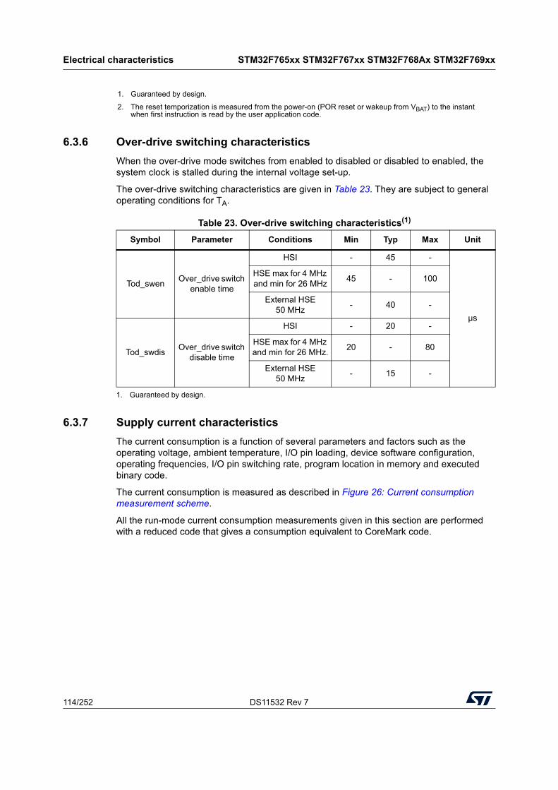
Electrical characteristics STM32F765xx STM32F767xx STM32F768Ax STM32F769xx
114/252 DS11532 Rev 7
6.3.6 Over-drive switching characteristics
When the over-drive mode switches from enabled to disabled or disabled to enabled, the system clock is stalled during the internal voltage set-up.
The over-drive switching characteristics are given in Table 23. They are subject to general operating conditions for TA.
6.3.7 Supply current characteristics
The current consumption is a function of several parameters and factors such as the operating voltage, ambient temperature, I/O pin loading, device software configuration, operating frequencies, I/O pin switching rate, program location in memory and executed binary code.
The current consumption is measured as described in Figure 26: Current consumption measurement scheme.
All the run-mode current consumption measurements given in this section are performed with a reduced code that gives a consumption equivalent to CoreMark code.
1. Guaranteed by design.
2. The reset temporization is measured from the power-on (POR reset or wakeup from VBAT) to the instant when first instruction is read by the user application code.
Table 23. Over-drive switching characteristics(1)
1. Guaranteed by design.
Symbol Parameter Conditions Min Typ Max Unit
Tod_swenOver_drive switch
enable time
HSI - 45 -
µs
HSE max for 4 MHz and min for 26 MHz
45 - 100
External HSE 50 MHz
- 40 -
Tod_swdisOver_drive switch
disable time
HSI - 20 -
HSE max for 4 MHz and min for 26 MHz.
20 - 80
External HSE 50 MHz
- 15 -
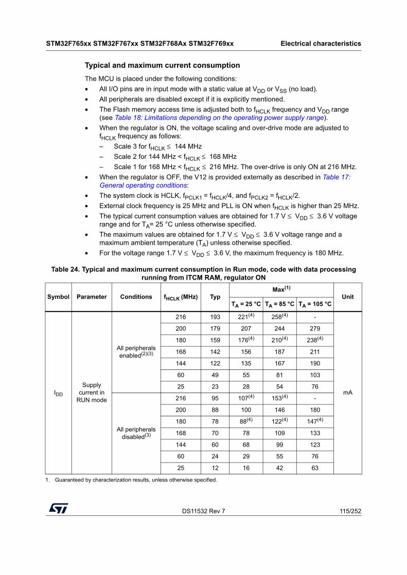
DS11532 Rev 7 115/252
STM32F765xx STM32F767xx STM32F768Ax STM32F769xx Electrical characteristics
218
Typical and maximum current consumption
The MCU is placed under the following conditions:
• All I/O pins are in input mode with a static value at VDD or VSS (no load).
• All peripherals are disabled except if it is explicitly mentioned.
• The Flash memory access time is adjusted both to fHCLK frequency and VDD range (see Table 18: Limitations depending on the operating power supply range).
• When the regulator is ON, the voltage scaling and over-drive mode are adjusted to fHCLK frequency as follows:
– Scale 3 for fHCLK ≤ 144 MHz
– Scale 2 for 144 MHz < fHCLK ≤ 168 MHz
– Scale 1 for 168 MHz < fHCLK ≤ 216 MHz. The over-drive is only ON at 216 MHz.
• When the regulator is OFF, the V12 is provided externally as described in Table 17: General operating conditions:
• The system clock is HCLK, fPCLK1 = fHCLK/4, and fPCLK2 = fHCLK/2.
• External clock frequency is 25 MHz and PLL is ON when fHCLK is higher than 25 MHz.
• The typical current consumption values are obtained for 1.7 V ≤ VDD ≤ 3.6 V voltage range and for TA= 25 °C unless otherwise specified.
• The maximum values are obtained for 1.7 V ≤ VDD ≤ 3.6 V voltage range and a maximum ambient temperature (TA) unless otherwise specified.
• For the voltage range 1.7 V ≤ VDD ≤ 3.6 V, the maximum frequency is 180 MHz.
Table 24. Typical and maximum current consumption in Run mode, code with data processing running from ITCM RAM, regulator ON
Symbol Parameter Conditions fHCLK (MHz) TypMax(1)
UnitTA = 25 °C TA = 85 °C TA = 105 °C
IDD
Supply current in
RUN mode
All peripherals enabled(2)(3)
216 193 221(4) 258(4) -
mA
200 179 207 244 279
180 159 176(4) 210(4) 238(4)
168 142 156 187 211
144 122 135 167 190
60 49 55 81 103
25 23 28 54 76
All peripherals disabled(3)
216 95 107(4) 153(4) -
200 88 100 146 180
180 78 88(4) 122(4) 147(4)
168 70 78 109 133
144 60 68 99 123
60 24 29 55 76
25 12 16 42 63
1. Guaranteed by characterization results, unless otherwise specified.
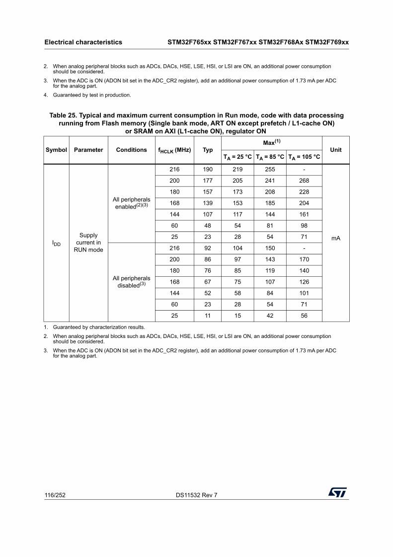
Electrical characteristics STM32F765xx STM32F767xx STM32F768Ax STM32F769xx
116/252 DS11532 Rev 7
2. When analog peripheral blocks such as ADCs, DACs, HSE, LSE, HSI, or LSI are ON, an additional power consumption should be considered.
3. When the ADC is ON (ADON bit set in the ADC_CR2 register), add an additional power consumption of 1.73 mA per ADC for the analog part.
4. Guaranteed by test in production.
Table 25. Typical and maximum current consumption in Run mode, code with data processingrunning from Flash memory (Single bank mode, ART ON except prefetch / L1-cache ON)
or SRAM on AXI (L1-cache ON), regulator ON
Symbol Parameter Conditions fHCLK (MHz) TypMax(1)
UnitTA = 25 °C TA = 85 °C TA = 105 °C
IDD
Supply current in
RUN mode
All peripherals enabled(2)(3)
216 190 219 255 -
mA
200 177 205 241 268
180 157 173 208 228
168 139 153 185 204
144 107 117 144 161
60 48 54 81 98
25 23 28 54 71
All peripherals disabled(3)
216 92 104 150 -
200 86 97 143 170
180 76 85 119 140
168 67 75 107 126
144 52 58 84 101
60 23 28 54 71
25 11 15 42 56
1. Guaranteed by characterization results.
2. When analog peripheral blocks such as ADCs, DACs, HSE, LSE, HSI, or LSI are ON, an additional power consumption should be considered.
3. When the ADC is ON (ADON bit set in the ADC_CR2 register), add an additional power consumption of 1.73 mA per ADC for the analog part.
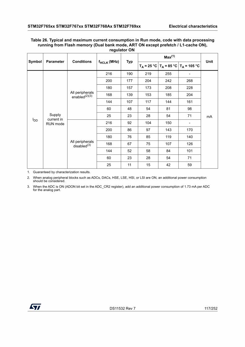
DS11532 Rev 7 117/252
STM32F765xx STM32F767xx STM32F768Ax STM32F769xx Electrical characteristics
218
Table 26. Typical and maximum current consumption in Run mode, code with data processingrunning from Flash memory (Dual bank mode, ART ON except prefetch / L1-cache ON),
regulator ON
Symbol Parameter Conditions fHCLK (MHz) TypMax(1)
UnitTA = 25 °C TA = 85 °C TA = 105 °C
IDD
Supply current in
RUN mode
All peripherals enabled(2)(3)
216 190 219 255 -
mA
200 177 204 242 268
180 157 173 208 228
168 139 153 185 204
144 107 117 144 161
60 48 54 81 98
25 23 28 54 71
All peripherals disabled(3)
216 92 104 150 -
200 86 97 143 170
180 76 85 119 140
168 67 75 107 126
144 52 58 84 101
60 23 28 54 71
25 11 15 42 59
1. Guaranteed by characterization results.
2. When analog peripheral blocks such as ADCs, DACs, HSE, LSE, HSI, or LSI are ON, an additional power consumption should be considered.
3. When the ADC is ON (ADON bit set in the ADC_CR2 register), add an additional power consumption of 1.73 mA per ADC for the analog part.
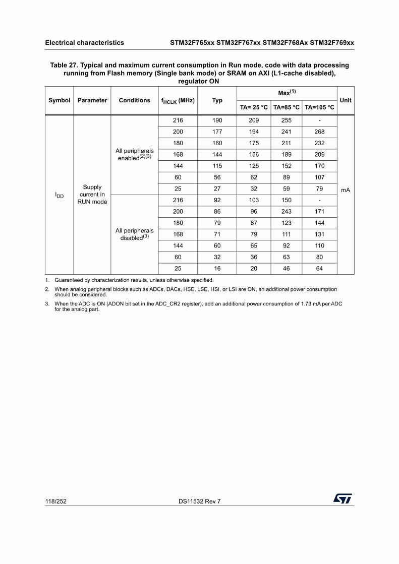
Electrical characteristics STM32F765xx STM32F767xx STM32F768Ax STM32F769xx
118/252 DS11532 Rev 7
Table 27. Typical and maximum current consumption in Run mode, code with data processingrunning from Flash memory (Single bank mode) or SRAM on AXI (L1-cache disabled),
regulator ON
Symbol Parameter Conditions fHCLK (MHz) TypMax(1)
UnitTA= 25 °C TA=85 °C TA=105 °C
IDD
Supply current in
RUN mode
All peripherals enabled(2)(3)
216 190 209 255 -
mA
200 177 194 241 268
180 160 175 211 232
168 144 156 189 209
144 115 125 152 170
60 56 62 89 107
25 27 32 59 79
All peripherals disabled(3)
216 92 103 150 -
200 86 96 243 171
180 79 87 123 144
168 71 79 111 131
144 60 65 92 110
60 32 36 63 80
25 16 20 46 64
1. Guaranteed by characterization results, unless otherwise specified.
2. When analog peripheral blocks such as ADCs, DACs, HSE, LSE, HSI, or LSI are ON, an additional power consumption should be considered.
3. When the ADC is ON (ADON bit set in the ADC_CR2 register), add an additional power consumption of 1.73 mA per ADC for the analog part.
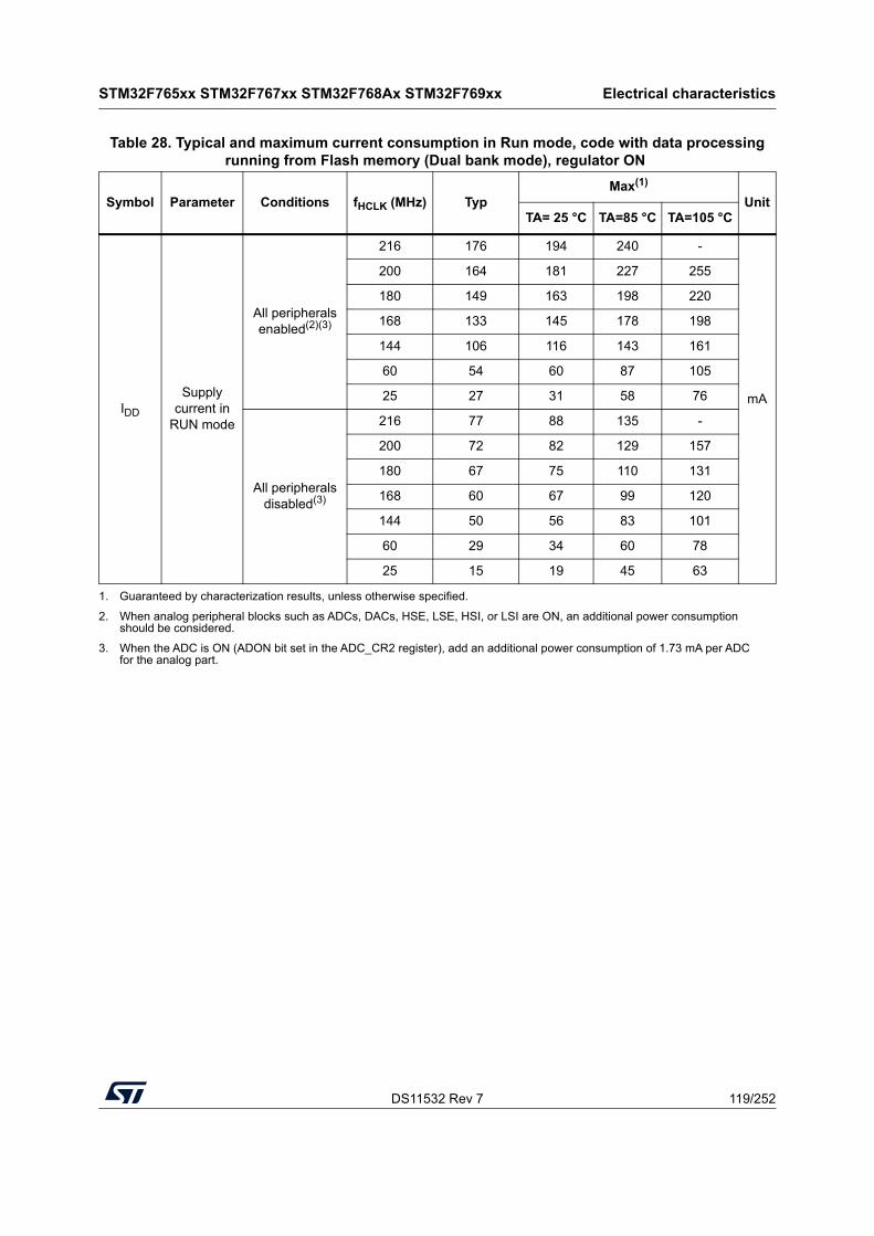
DS11532 Rev 7 119/252
STM32F765xx STM32F767xx STM32F768Ax STM32F769xx Electrical characteristics
218
Table 28. Typical and maximum current consumption in Run mode, code with data processingrunning from Flash memory (Dual bank mode), regulator ON
Symbol Parameter Conditions fHCLK (MHz) TypMax(1)
UnitTA= 25 °C TA=85 °C TA=105 °C
IDD
Supply current in
RUN mode
All peripherals enabled(2)(3)
216 176 194 240 -
mA
200 164 181 227 255
180 149 163 198 220
168 133 145 178 198
144 106 116 143 161
60 54 60 87 105
25 27 31 58 76
All peripherals disabled(3)
216 77 88 135 -
200 72 82 129 157
180 67 75 110 131
168 60 67 99 120
144 50 56 83 101
60 29 34 60 78
25 15 19 45 63
1. Guaranteed by characterization results, unless otherwise specified.
2. When analog peripheral blocks such as ADCs, DACs, HSE, LSE, HSI, or LSI are ON, an additional power consumption should be considered.
3. When the ADC is ON (ADON bit set in the ADC_CR2 register), add an additional power consumption of 1.73 mA per ADC for the analog part.
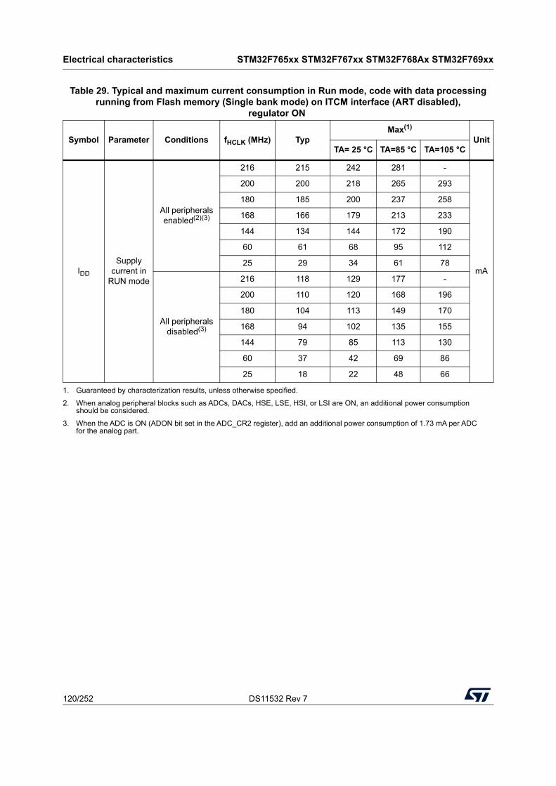
Electrical characteristics STM32F765xx STM32F767xx STM32F768Ax STM32F769xx
120/252 DS11532 Rev 7
Table 29. Typical and maximum current consumption in Run mode, code with data processingrunning from Flash memory (Single bank mode) on ITCM interface (ART disabled),
regulator ON
Symbol Parameter Conditions fHCLK (MHz) TypMax(1)
UnitTA= 25 °C TA=85 °C TA=105 °C
IDD
Supply current in
RUN mode
All peripherals enabled(2)(3)
216 215 242 281 -
mA
200 200 218 265 293
180 185 200 237 258
168 166 179 213 233
144 134 144 172 190
60 61 68 95 112
25 29 34 61 78
All peripherals disabled(3)
216 118 129 177 -
200 110 120 168 196
180 104 113 149 170
168 94 102 135 155
144 79 85 113 130
60 37 42 69 86
25 18 22 48 66
1. Guaranteed by characterization results, unless otherwise specified.
2. When analog peripheral blocks such as ADCs, DACs, HSE, LSE, HSI, or LSI are ON, an additional power consumption should be considered.
3. When the ADC is ON (ADON bit set in the ADC_CR2 register), add an additional power consumption of 1.73 mA per ADC for the analog part.
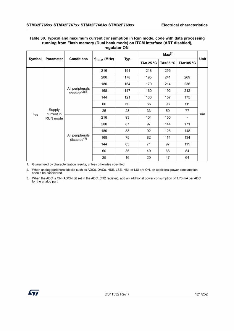
DS11532 Rev 7 121/252
STM32F765xx STM32F767xx STM32F768Ax STM32F769xx Electrical characteristics
218
Table 30. Typical and maximum current consumption in Run mode, code with data processingrunning from Flash memory (Dual bank mode) on ITCM interface (ART disabled),
regulator ON
Symbol Parameter Conditions fHCLK (MHz) TypMax(1)
UnitTA= 25 °C TA=85 °C TA=105 °C
IDD
Supply current in
RUN mode
All peripherals enabled(2)(3)
216 191 218 255 -
mA
200 178 195 241 269
180 164 179 214 236
168 147 160 192 212
144 121 130 157 175
60 60 66 93 111
25 28 33 59 77
All peripherals disabled(3)
216 93 104 150 -
200 87 97 144 171
180 83 92 126 148
168 75 82 114 134
144 65 71 97 115
60 35 40 66 84
25 16 20 47 64
1. Guaranteed by characterization results, unless otherwise specified.
2. When analog peripheral blocks such as ADCs, DACs, HSE, LSE, HSI, or LSI are ON, an additional power consumption should be considered.
3. When the ADC is ON (ADON bit set in the ADC_CR2 register), add an additional power consumption of 1.73 mA per ADC for the analog part.
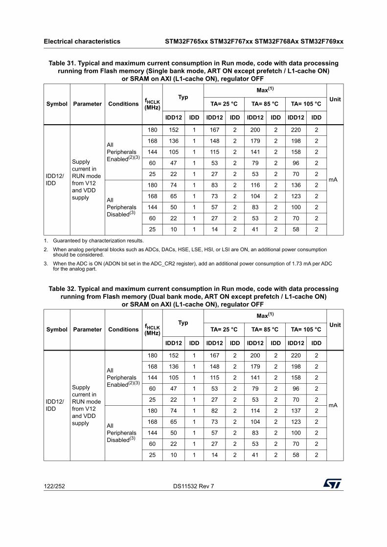
Electrical characteristics STM32F765xx STM32F767xx STM32F768Ax STM32F769xx
122/252 DS11532 Rev 7
Table 31. Typical and maximum current consumption in Run mode, code with data processingrunning from Flash memory (Single bank mode, ART ON except prefetch / L1-cache ON)
or SRAM on AXI (L1-cache ON), regulator OFF
Symbol Parameter ConditionsfHCLK (MHz)
TypMax(1)
UnitTA= 25 °C TA= 85 °C TA= 105 °C
IDD12 IDD IDD12 IDD IDD12 IDD IDD12 IDD
IDD12/ IDD
Supply current in RUN mode from V12 and VDD supply
All Peripherals Enabled(2)(3)
180 152 1 167 2 200 2 220 2
mA
168 136 1 148 2 179 2 198 2
144 105 1 115 2 141 2 158 2
60 47 1 53 2 79 2 96 2
25 22 1 27 2 53 2 70 2
All Peripherals Disabled(3)
180 74 1 83 2 116 2 136 2
168 65 1 73 2 104 2 123 2
144 50 1 57 2 83 2 100 2
60 22 1 27 2 53 2 70 2
25 10 1 14 2 41 2 58 2
1. Guaranteed by characterization results.
2. When analog peripheral blocks such as ADCs, DACs, HSE, LSE, HSI, or LSI are ON, an additional power consumption should be considered.
3. When the ADC is ON (ADON bit set in the ADC_CR2 register), add an additional power consumption of 1.73 mA per ADC for the analog part.
Table 32. Typical and maximum current consumption in Run mode, code with data processingrunning from Flash memory (Dual bank mode, ART ON except prefetch / L1-cache ON)
or SRAM on AXI (L1-cache ON), regulator OFF
Symbol Parameter ConditionsfHCLK (MHz)
TypMax(1)
UnitTA= 25 °C TA= 85 °C TA= 105 °C
IDD12 IDD IDD12 IDD IDD12 IDD IDD12 IDD
IDD12/ IDD
Supply current in RUN mode from V12 and VDD supply
All Peripherals Enabled(2)(3)
180 152 1 167 2 200 2 220 2
mA
168 136 1 148 2 179 2 198 2
144 105 1 115 2 141 2 158 2
60 47 1 53 2 79 2 96 2
25 22 1 27 2 53 2 70 2
All Peripherals Disabled(3)
180 74 1 82 2 114 2 137 2
168 65 1 73 2 104 2 123 2
144 50 1 57 2 83 2 100 2
60 22 1 27 2 53 2 70 2
25 10 1 14 2 41 2 58 2
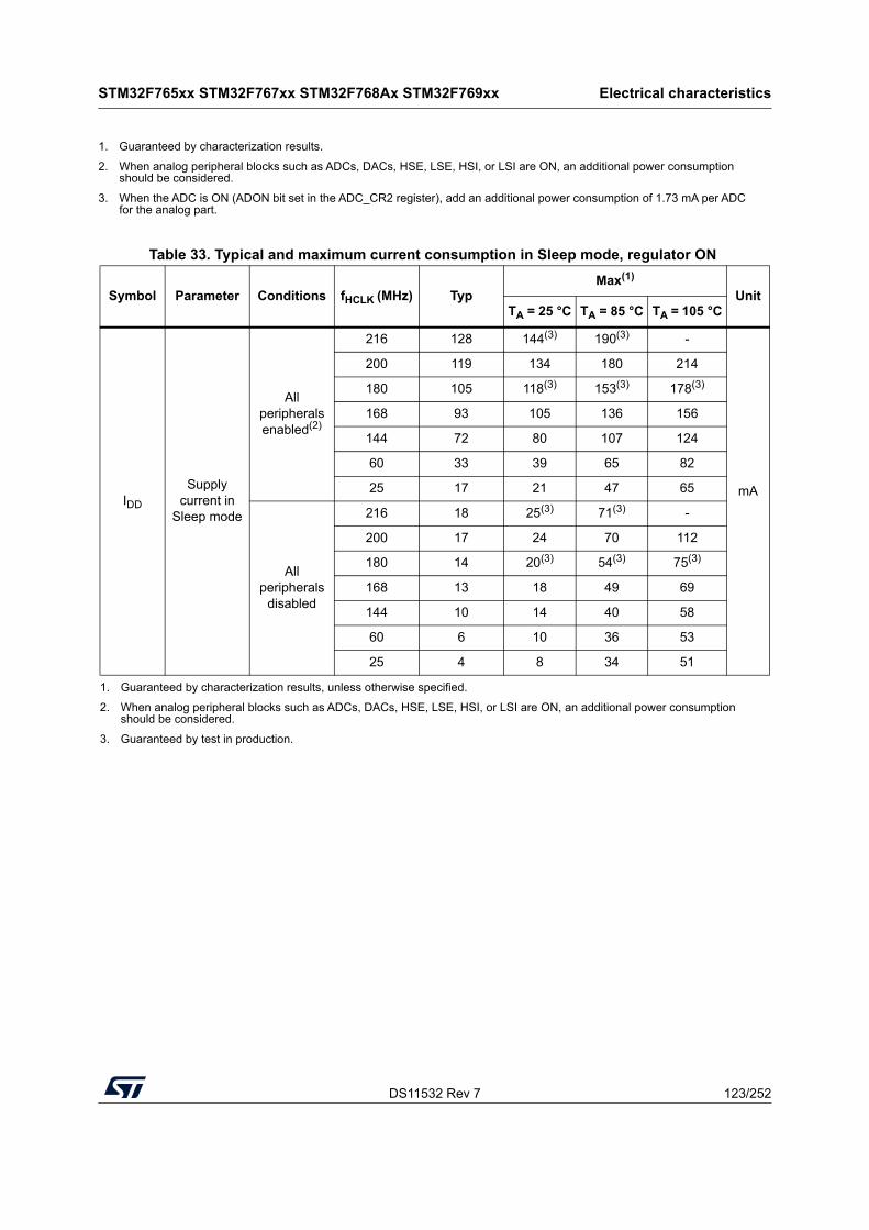
DS11532 Rev 7 123/252
STM32F765xx STM32F767xx STM32F768Ax STM32F769xx Electrical characteristics
218
1. Guaranteed by characterization results.
2. When analog peripheral blocks such as ADCs, DACs, HSE, LSE, HSI, or LSI are ON, an additional power consumption should be considered.
3. When the ADC is ON (ADON bit set in the ADC_CR2 register), add an additional power consumption of 1.73 mA per ADC for the analog part.
Table 33. Typical and maximum current consumption in Sleep mode, regulator ON
Symbol Parameter Conditions fHCLK (MHz) TypMax(1)
UnitTA = 25 °C TA = 85 °C TA = 105 °C
IDD
Supply current in
Sleep mode
All peripherals enabled(2)
216 128 144(3) 190(3) -
mA
200 119 134 180 214
180 105 118(3) 153(3) 178(3)
168 93 105 136 156
144 72 80 107 124
60 33 39 65 82
25 17 21 47 65
All peripherals
disabled
216 18 25(3) 71(3) -
200 17 24 70 112
180 14 20(3) 54(3) 75(3)
168 13 18 49 69
144 10 14 40 58
60 6 10 36 53
25 4 8 34 51
1. Guaranteed by characterization results, unless otherwise specified.
2. When analog peripheral blocks such as ADCs, DACs, HSE, LSE, HSI, or LSI are ON, an additional power consumption should be considered.
3. Guaranteed by test in production.
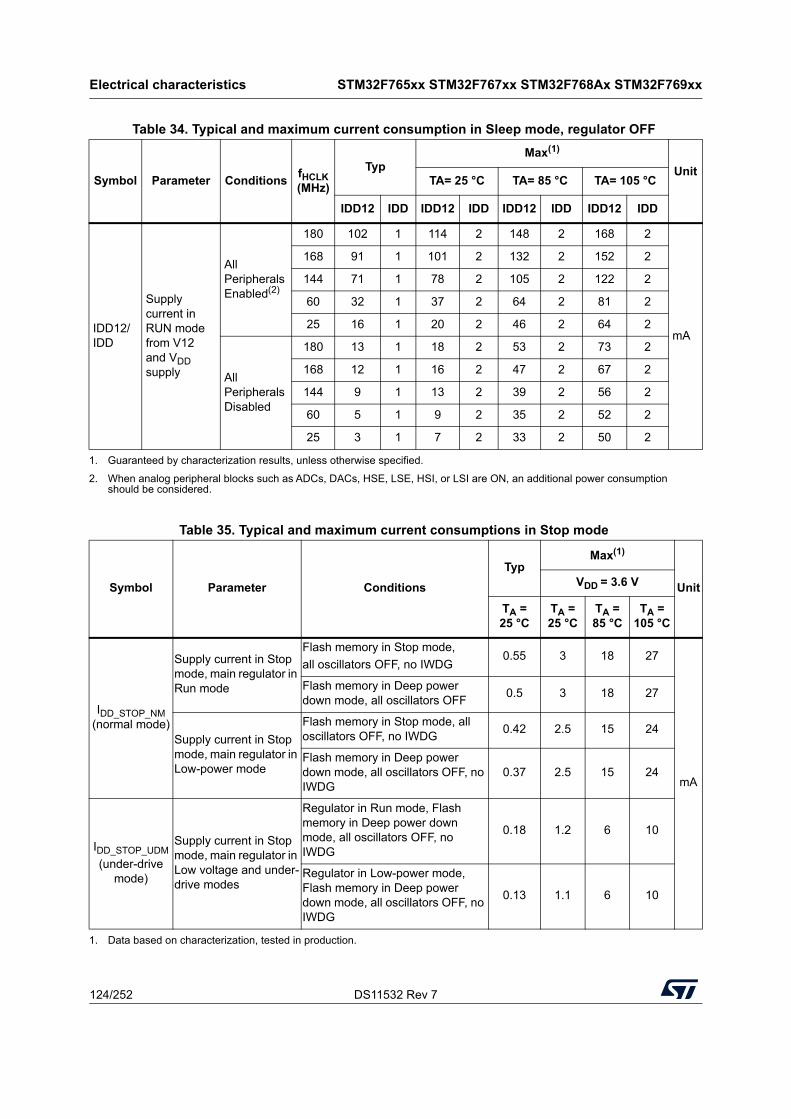
Electrical characteristics STM32F765xx STM32F767xx STM32F768Ax STM32F769xx
124/252 DS11532 Rev 7
Table 34. Typical and maximum current consumption in Sleep mode, regulator OFF
Symbol Parameter ConditionsfHCLK (MHz)
TypMax(1)
UnitTA= 25 °C TA= 85 °C TA= 105 °C
IDD12 IDD IDD12 IDD IDD12 IDD IDD12 IDD
IDD12/ IDD
Supply current in RUN mode from V12 and VDD supply
All Peripherals Enabled(2)
180 102 1 114 2 148 2 168 2
mA
168 91 1 101 2 132 2 152 2
144 71 1 78 2 105 2 122 2
60 32 1 37 2 64 2 81 2
25 16 1 20 2 46 2 64 2
All Peripherals Disabled
180 13 1 18 2 53 2 73 2
168 12 1 16 2 47 2 67 2
144 9 1 13 2 39 2 56 2
60 5 1 9 2 35 2 52 2
25 3 1 7 2 33 2 50 2
1. Guaranteed by characterization results, unless otherwise specified.
2. When analog peripheral blocks such as ADCs, DACs, HSE, LSE, HSI, or LSI are ON, an additional power consumption should be considered.
Table 35. Typical and maximum current consumptions in Stop mode
Symbol Parameter Conditions
TypMax(1)
UnitVDD = 3.6 V
TA = 25 °C
TA = 25 °C
TA = 85 °C
TA = 105 °C
IDD_STOP_NM (normal mode)
Supply current in Stop mode, main regulator in Run mode
Flash memory in Stop mode,
all oscillators OFF, no IWDG0.55 3 18 27
mA
Flash memory in Deep power down mode, all oscillators OFF
0.5 3 18 27
Supply current in Stop mode, main regulator in Low-power mode
Flash memory in Stop mode, all oscillators OFF, no IWDG
0.42 2.5 15 24
Flash memory in Deep power down mode, all oscillators OFF, no IWDG
0.37 2.5 15 24
IDD_STOP_UDM
(under-drive mode)
Supply current in Stop mode, main regulator in Low voltage and under-drive modes
Regulator in Run mode, Flash memory in Deep power down mode, all oscillators OFF, no IWDG
0.18 1.2 6 10
Regulator in Low-power mode, Flash memory in Deep power down mode, all oscillators OFF, no IWDG
0.13 1.1 6 10
1. Data based on characterization, tested in production.
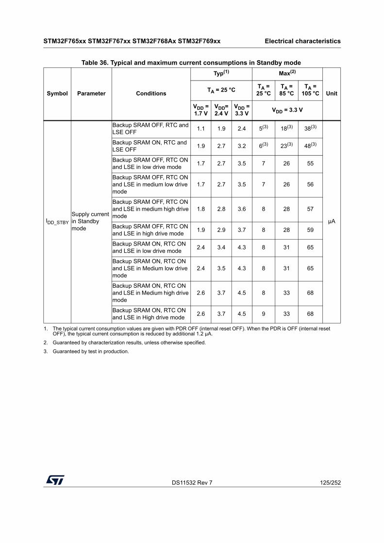
DS11532 Rev 7 125/252
STM32F765xx STM32F767xx STM32F768Ax STM32F769xx Electrical characteristics
218
Table 36. Typical and maximum current consumptions in Standby mode
Symbol Parameter Conditions
Typ(1) Max(2)
UnitTA = 25 °C
TA = 25 °C
TA = 85 °C
TA = 105 °C
VDD = 1.7 V
VDD= 2.4 V
VDD = 3.3 V
VDD = 3.3 V
IDD_STBY
Supply current in Standby mode
Backup SRAM OFF, RTC and LSE OFF
1.1 1.9 2.4 5(3) 18(3) 38(3)
µA
Backup SRAM ON, RTC and LSE OFF
1.9 2.7 3.2 6(3) 23(3) 48(3)
Backup SRAM OFF, RTC ON and LSE in low drive mode
1.7 2.7 3.5 7 26 55
Backup SRAM OFF, RTC ON and LSE in medium low drive mode
1.7 2.7 3.5 7 26 56
Backup SRAM OFF, RTC ON and LSE in medium high drive mode
1.8 2.8 3.6 8 28 57
Backup SRAM OFF, RTC ON and LSE in high drive mode
1.9 2.9 3.7 8 28 59
Backup SRAM ON, RTC ON and LSE in low drive mode
2.4 3.4 4.3 8 31 65
Backup SRAM ON, RTC ON and LSE in Medium low drive mode
2.4 3.5 4.3 8 31 65
Backup SRAM ON, RTC ON and LSE in Medium high drive mode
2.6 3.7 4.5 8 33 68
Backup SRAM ON, RTC ON and LSE in High drive mode
2.6 3.7 4.5 9 33 68
1. The typical current consumption values are given with PDR OFF (internal reset OFF). When the PDR is OFF (internal reset OFF), the typical current consumption is reduced by additional 1.2 µA.
2. Guaranteed by characterization results, unless otherwise specified.
3. Guaranteed by test in production.
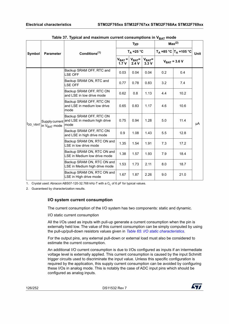
Electrical characteristics STM32F765xx STM32F767xx STM32F768Ax STM32F769xx
126/252 DS11532 Rev 7
I/O system current consumption
The current consumption of the I/O system has two components: static and dynamic.
I/O static current consumption
All the I/Os used as inputs with pull-up generate a current consumption when the pin is externally held low. The value of this current consumption can be simply computed by using the pull-up/pull-down resistors values given in Table 65: I/O static characteristics.
For the output pins, any external pull-down or external load must also be considered to estimate the current consumption.
An additional I/O current consumption is due to I/Os configured as inputs if an intermediate voltage level is externally applied. This current consumption is caused by the input Schmitt trigger circuits used to discriminate the input value. Unless this specific configuration is required by the application, this supply current consumption can be avoided by configuring these I/Os in analog mode. This is notably the case of ADC input pins which should be configured as analog inputs.
Table 37. Typical and maximum current consumptions in VBAT mode
Symbol Parameter Conditions(1)
Typ Max(2)
UnitTA =25 °C TA =85 °C TA =105 °C
VBAT = 1.7 V
VBAT= 2.4 V
VBAT= 3.3 V
VBAT = 3.6 V
IDD_VBATSupply current in VBAT mode
Backup SRAM OFF, RTC and LSE OFF
0.03 0.04 0.04 0.2 0.4
µA
Backup SRAM ON, RTC and LSE OFF
0.77 0.78 0.83 3.2 7.4
Backup SRAM OFF, RTC ON and LSE in low drive mode
0.62 0.8 1.13 4.4 10.2
Backup SRAM OFF, RTC ON and LSE in medium low drive mode
0.65 0.83 1.17 4.6 10.6
Backup SRAM OFF, RTC ON and LSE in medium high drive mode
0.75 0.94 1.28 5.0 11.4
Backup SRAM OFF, RTC ON and LSE in high drive mode
0.9 1.08 1.43 5.5 12.8
Backup SRAM ON, RTC ON and LSE in low drive mode
1.35 1.54 1.91 7.3 17.2
Backup SRAM ON, RTC ON and LSE in Medium low drive mode
1.38 1.57 1.93 7.9 18.4
Backup SRAM ON, RTC ON and LSE in Medium high drive mode
1.53 1.73 2.11 8.0 18.7
Backup SRAM ON, RTC ON and LSE in High drive mode
1.67 1.87 2.26 9.0 21.0
1. Crystal used: Abracon ABS07-120-32.768 kHz-T with a CL of 6 pF for typical values.
2. Guaranteed by characterization results.
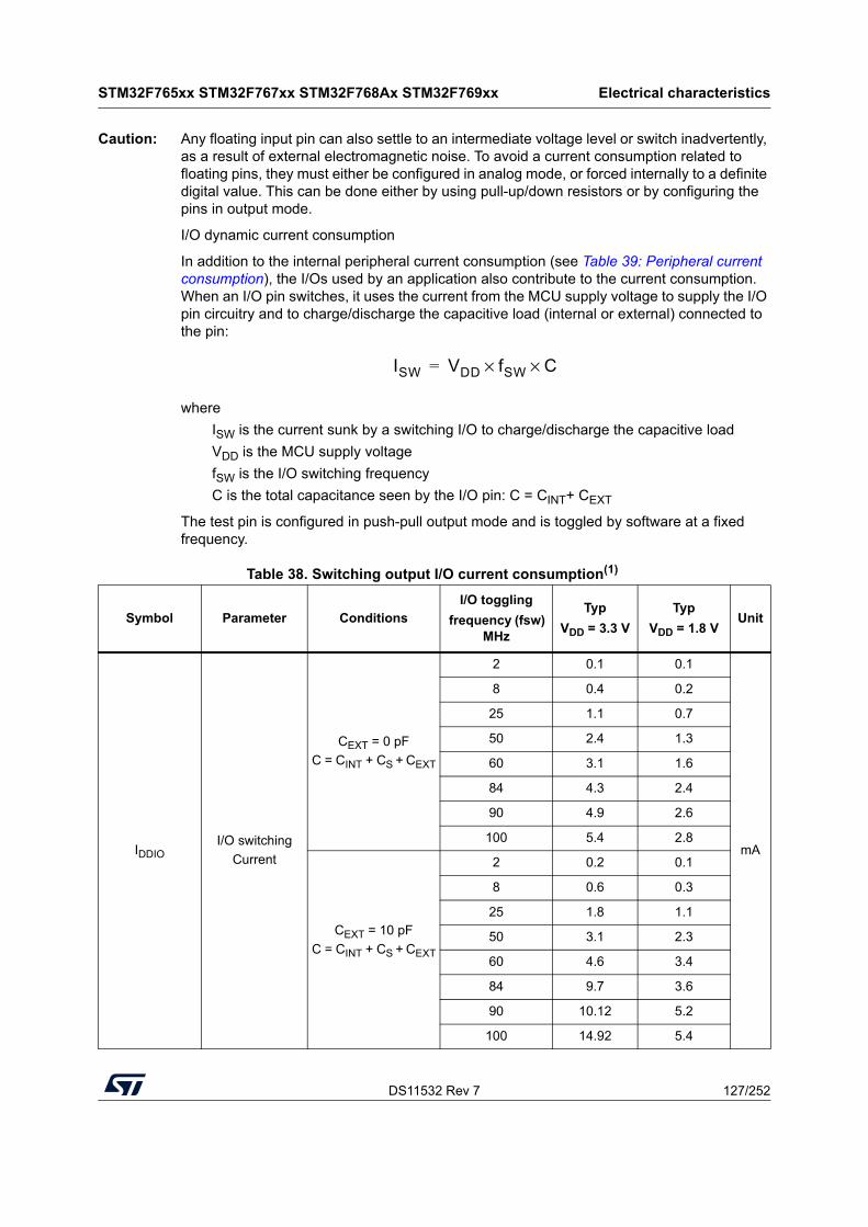
DS11532 Rev 7 127/252
STM32F765xx STM32F767xx STM32F768Ax STM32F769xx Electrical characteristics
218
Caution: Any floating input pin can also settle to an intermediate voltage level or switch inadvertently, as a result of external electromagnetic noise. To avoid a current consumption related to floating pins, they must either be configured in analog mode, or forced internally to a definite digital value. This can be done either by using pull-up/down resistors or by configuring the pins in output mode.
I/O dynamic current consumption
In addition to the internal peripheral current consumption (see Table 39: Peripheral current consumption), the I/Os used by an application also contribute to the current consumption. When an I/O pin switches, it uses the current from the MCU supply voltage to supply the I/O pin circuitry and to charge/discharge the capacitive load (internal or external) connected to the pin:
where
ISW is the current sunk by a switching I/O to charge/discharge the capacitive load
VDD is the MCU supply voltage
fSW is the I/O switching frequency
C is the total capacitance seen by the I/O pin: C = CINT+ CEXT
The test pin is configured in push-pull output mode and is toggled by software at a fixed frequency.
ISW VDD fSW C××=
Table 38. Switching output I/O current consumption(1)
Symbol Parameter ConditionsI/O toggling
frequency (fsw) MHz
Typ
VDD = 3.3 V
Typ
VDD = 1.8 VUnit
IDDIOI/O switching
Current
CEXT = 0 pF
C = CINT + CS + CEXT
2 0.1 0.1
mA
8 0.4 0.2
25 1.1 0.7
50 2.4 1.3
60 3.1 1.6
84 4.3 2.4
90 4.9 2.6
100 5.4 2.8
CEXT = 10 pF
C = CINT + CS + CEXT
2 0.2 0.1
8 0.6 0.3
25 1.8 1.1
50 3.1 2.3
60 4.6 3.4
84 9.7 3.6
90 10.12 5.2
100 14.92 5.4
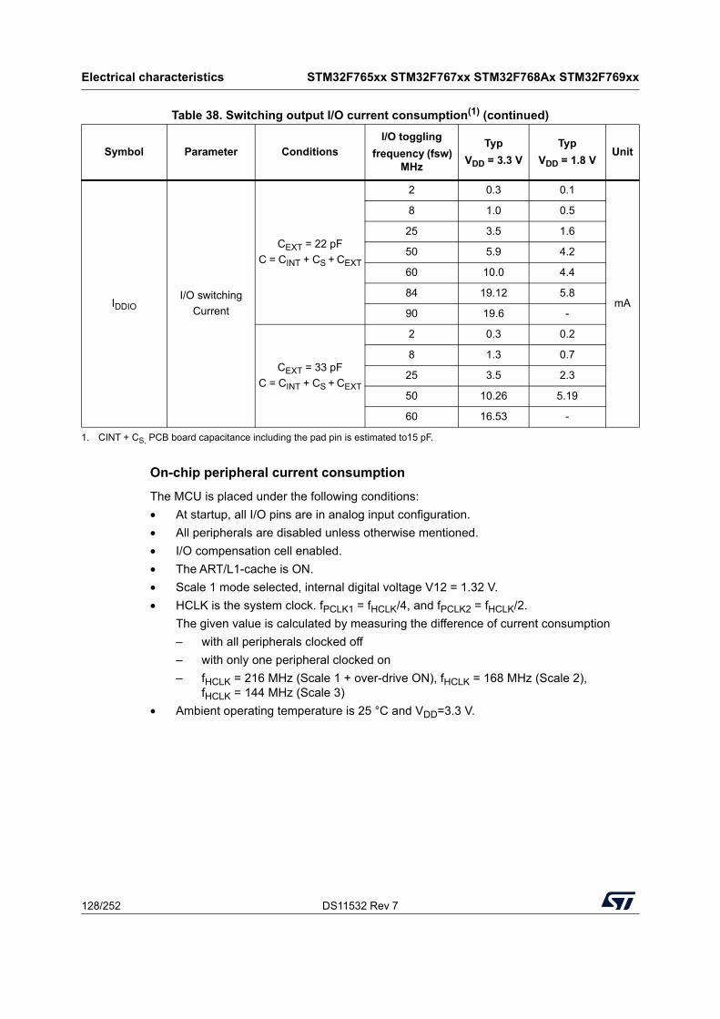
Electrical characteristics STM32F765xx STM32F767xx STM32F768Ax STM32F769xx
128/252 DS11532 Rev 7
On-chip peripheral current consumption
The MCU is placed under the following conditions:
• At startup, all I/O pins are in analog input configuration.
• All peripherals are disabled unless otherwise mentioned.
• I/O compensation cell enabled.
• The ART/L1-cache is ON.
• Scale 1 mode selected, internal digital voltage V12 = 1.32 V.
• HCLK is the system clock. fPCLK1 = fHCLK/4, and fPCLK2 = fHCLK/2.
The given value is calculated by measuring the difference of current consumption
– with all peripherals clocked off
– with only one peripheral clocked on
– fHCLK = 216 MHz (Scale 1 + over-drive ON), fHCLK = 168 MHz (Scale 2), fHCLK = 144 MHz (Scale 3)
• Ambient operating temperature is 25 °C and VDD=3.3 V.
IDDIOI/O switching
Current
CEXT = 22 pF
C = CINT + CS + CEXT
2 0.3 0.1
mA
8 1.0 0.5
25 3.5 1.6
50 5.9 4.2
60 10.0 4.4
84 19.12 5.8
90 19.6 -
CEXT = 33 pF
C = CINT + CS + CEXT
2 0.3 0.2
8 1.3 0.7
25 3.5 2.3
50 10.26 5.19
60 16.53 -
1. CINT + CS, PCB board capacitance including the pad pin is estimated to15 pF.
Table 38. Switching output I/O current consumption(1) (continued)
Symbol Parameter ConditionsI/O toggling
frequency (fsw) MHz
Typ
VDD = 3.3 V
Typ
VDD = 1.8 VUnit
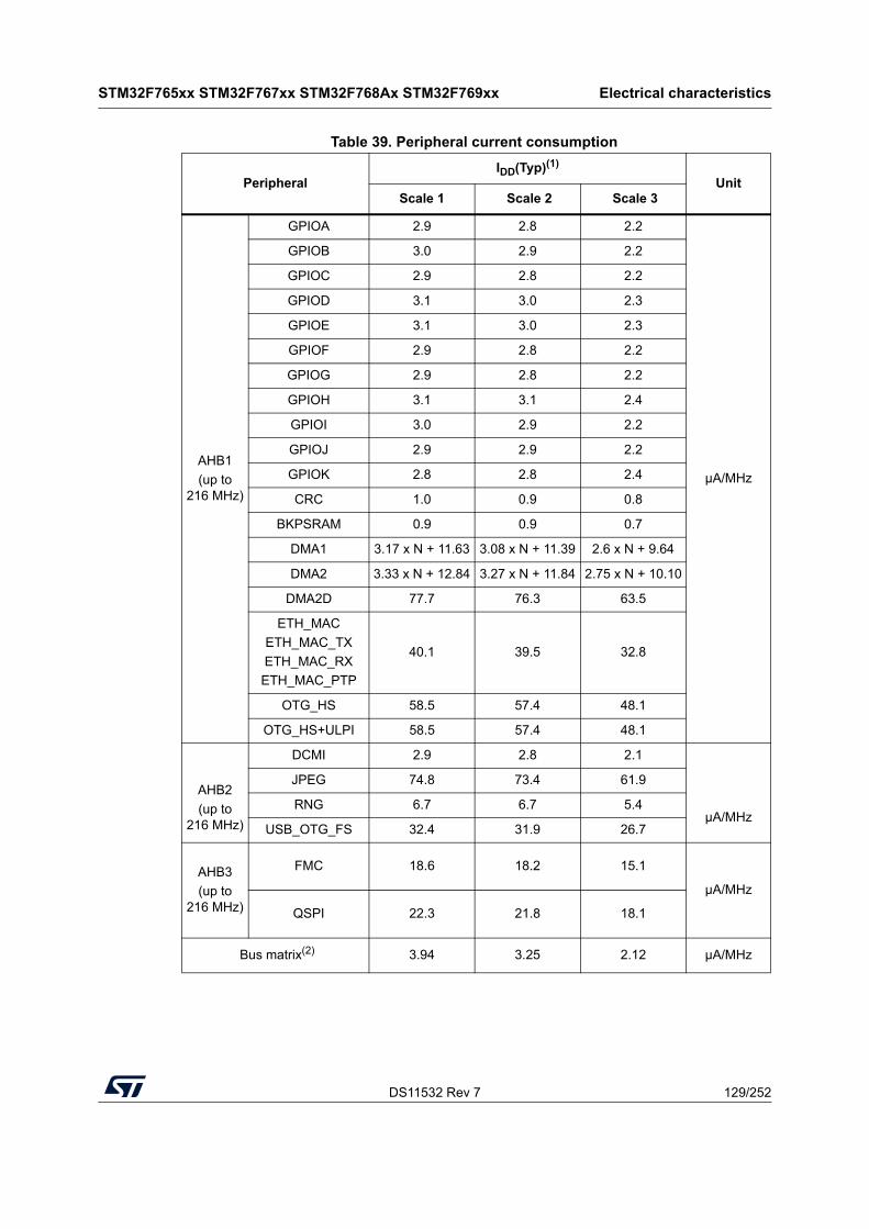
DS11532 Rev 7 129/252
STM32F765xx STM32F767xx STM32F768Ax STM32F769xx Electrical characteristics
218
Table 39. Peripheral current consumption
PeripheralIDD(Typ)(1)
UnitScale 1 Scale 2 Scale 3
AHB1
(up to 216 MHz)
GPIOA 2.9 2.8 2.2
µA/MHz
GPIOB 3.0 2.9 2.2
GPIOC 2.9 2.8 2.2
GPIOD 3.1 3.0 2.3
GPIOE 3.1 3.0 2.3
GPIOF 2.9 2.8 2.2
GPIOG 2.9 2.8 2.2
GPIOH 3.1 3.1 2.4
GPIOI 3.0 2.9 2.2
GPIOJ 2.9 2.9 2.2
GPIOK 2.8 2.8 2.4
CRC 1.0 0.9 0.8
BKPSRAM 0.9 0.9 0.7
DMA1 3.17 x N + 11.63 3.08 x N + 11.39 2.6 x N + 9.64
DMA2 3.33 x N + 12.84 3.27 x N + 11.84 2.75 x N + 10.10
DMA2D 77.7 76.3 63.5
ETH_MAC
ETH_MAC_TX
ETH_MAC_RX
ETH_MAC_PTP
40.1 39.5 32.8
OTG_HS 58.5 57.4 48.1
OTG_HS+ULPI 58.5 57.4 48.1
AHB2
(up to 216 MHz)
DCMI 2.9 2.8 2.1
µA/MHz
JPEG 74.8 73.4 61.9
RNG 6.7 6.7 5.4
USB_OTG_FS 32.4 31.9 26.7
AHB3
(up to 216 MHz)
FMC 18.6 18.2 15.1
µA/MHz
QSPI 22.3 21.8 18.1
Bus matrix(2) 3.94 3.25 2.12 µA/MHz
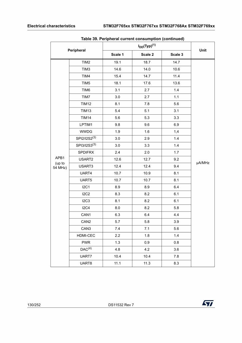
Electrical characteristics STM32F765xx STM32F767xx STM32F768Ax STM32F769xx
130/252 DS11532 Rev 7
APB1
(up to 54 MHz)
TIM2 19.1 18.7 14.7
µA/MHz
TIM3 14.6 14.0 10.6
TIM4 15.4 14.7 11.4
TIM5 18.1 17.6 13.6
TIM6 3.1 2.7 1.4
TIM7 3.0 2.7 1.1
TIM12 8.1 7.8 5.6
TIM13 5.4 5.1 3.1
TIM14 5.6 5.3 3.3
LPTIM1 9.8 9.6 6.9
WWDG 1.9 1.6 1,4
SPI2/I2S2(3) 3.0 2.9 1.4
SPI3/I2S3(3) 3.0 3.3 1.4
SPDIFRX 2.4 2.0 1.7
USART2 12.6 12.7 9.2
USART3 12.4 12.4 9.4
UART4 10.7 10.9 8.1
UART5 10.7 10.7 8.1
I2C1 8.9 8.9 6.4
I2C2 8.3 8.2 6.1
I2C3 8.1 8.2 6.1
I2C4 8.0 8.2 5.8
CAN1 6.3 6.4 4.4
CAN2 5.7 5.8 3.9
CAN3 7.4 7.1 5.6
HDMI-CEC 2.2 1.8 1.4
PWR 1.3 0.9 0.8
DAC(4) 4.8 4.2 3.6
UART7 10.4 10.4 7.8
UART8 11.1 11.3 8.3
Table 39. Peripheral current consumption (continued)
PeripheralIDD(Typ)(1)
UnitScale 1 Scale 2 Scale 3
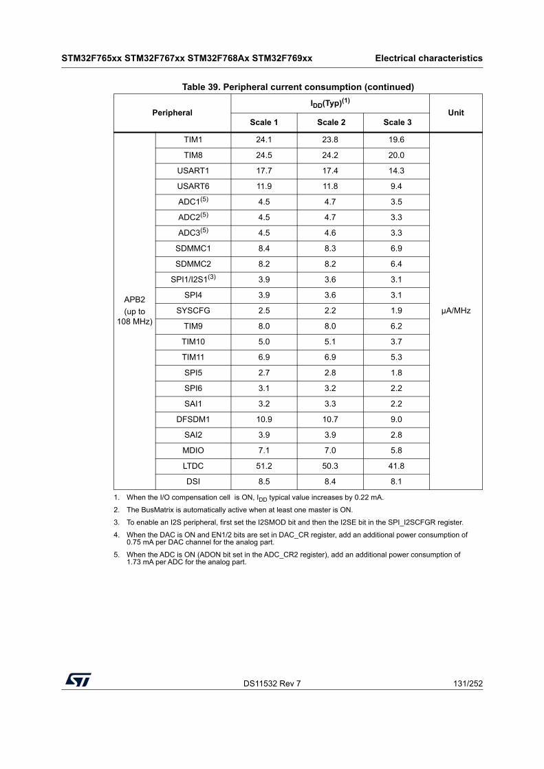
DS11532 Rev 7 131/252
STM32F765xx STM32F767xx STM32F768Ax STM32F769xx Electrical characteristics
218
APB2
(up to 108 MHz)
TIM1 24.1 23.8 19.6
µA/MHz
TIM8 24.5 24.2 20.0
USART1 17.7 17.4 14.3
USART6 11.9 11.8 9.4
ADC1(5) 4.5 4.7 3.5
ADC2(5) 4.5 4.7 3.3
ADC3(5) 4.5 4.6 3.3
SDMMC1 8.4 8.3 6.9
SDMMC2 8.2 8.2 6.4
SPI1/I2S1(3) 3.9 3.6 3.1
SPI4 3.9 3.6 3.1
SYSCFG 2.5 2.2 1.9
TIM9 8.0 8.0 6.2
TIM10 5.0 5.1 3.7
TIM11 6.9 6.9 5.3
SPI5 2.7 2.8 1.8
SPI6 3.1 3.2 2.2
SAI1 3.2 3.3 2.2
DFSDM1 10.9 10.7 9.0
SAI2 3.9 3.9 2.8
MDIO 7.1 7.0 5.8
LTDC 51.2 50.3 41.8
DSI 8.5 8.4 8.1
1. When the I/O compensation cell is ON, IDD typical value increases by 0.22 mA.
2. The BusMatrix is automatically active when at least one master is ON.
3. To enable an I2S peripheral, first set the I2SMOD bit and then the I2SE bit in the SPI_I2SCFGR register.
4. When the DAC is ON and EN1/2 bits are set in DAC_CR register, add an additional power consumption of 0.75 mA per DAC channel for the analog part.
5. When the ADC is ON (ADON bit set in the ADC_CR2 register), add an additional power consumption of 1.73 mA per ADC for the analog part.
Table 39. Peripheral current consumption (continued)
PeripheralIDD(Typ)(1)
UnitScale 1 Scale 2 Scale 3
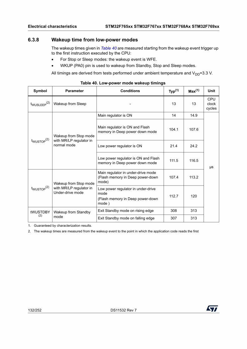
Electrical characteristics STM32F765xx STM32F767xx STM32F768Ax STM32F769xx
132/252 DS11532 Rev 7
6.3.8 Wakeup time from low-power modes
The wakeup times given in Table 40 are measured starting from the wakeup event trigger up to the first instruction executed by the CPU:
• For Stop or Sleep modes: the wakeup event is WFE.
• WKUP (PA0) pin is used to wakeup from Standby, Stop and Sleep modes.
All timings are derived from tests performed under ambient temperature and VDD=3.3 V.
Table 40. Low-power mode wakeup timings
Symbol Parameter Conditions Typ(1) Max(1) Unit
tWUSLEEP(2) Wakeup from Sleep - 13 13
CPU clock cycles
tWUSTOP(2)
Wakeup from Stop mode with MR/LP regulator in normal mode
Main regulator is ON 14 14.9
µs
Main regulator is ON and Flash memory in Deep power down mode
104.1 107.6
Low power regulator is ON 21.4 24.2
Low power regulator is ON and Flash memory in Deep power down mode
111.5 116.5
tWUSTOP(2)
Wakeup from Stop mode with MR/LP regulator in Under-drive mode
Main regulator in under-drive mode (Flash memory in Deep power-down mode)
107.4 113.2
Low power regulator in under-drive mode
(Flash memory in Deep power-down mode )
112.7 120
tWUSTDBY (2)
Wakeup from Standby mode
Exit Standby mode on rising edge 308 313
Exit Standby mode on falling edge 307 313
1. Guaranteed by characterization results.
2. The wakeup times are measured from the wakeup event to the point in which the application code reads the first
DS11532 Rev 7 133/252
STM32F765xx STM32F767xx STM32F768Ax STM32F769xx Electrical characteristics
218
6.3.9 External clock source characteristics
High-speed external user clock generated from an external source
In bypass mode the HSE oscillator is switched off and the input pin is a standard I/O. The external clock signal has to respect the Table 65: I/O static characteristics. However, the recommended clock input waveform is shown in Figure 28.
The characteristics given in Table 41 result from tests performed using an high-speed external clock source, and under ambient temperature and supply voltage conditions summarized in Table 17.
Low-speed external user clock generated from an external source
In bypass mode the LSE oscillator is switched off and the input pin is a standard I/O. The external clock signal has to respect the Table 65: I/O static characteristics. However, the recommended clock input waveform is shown in Figure 29.
The characteristics given in Table 42 result from tests performed using an low-speed external clock source, and under ambient temperature and supply voltage conditions summarized in Table 17.
Table 41. High-speed external user clock characteristics
Symbol Parameter Conditions Min Typ Max Unit
fHSE_extExternal user clock source frequency(1)
-
1 - 50 MHz
VHSEH OSC_IN input pin high level voltage 0.7VDD - VDDV
VHSEL OSC_IN input pin low level voltage VSS - 0.3VDD
tw(HSE)tw(HSE)
OSC_IN high or low time(1)
1. Guaranteed by design.
5 - -
nstr(HSE)tf(HSE)
OSC_IN rise or fall time(1) - - 10
Cin(HSE) OSC_IN input capacitance(1) - - 5 - pF
DuCy(HSE) Duty cycle - 45 - 55 %
IL OSC_IN Input leakage current VSS ≤ VIN ≤ VDD - - ±1 µA
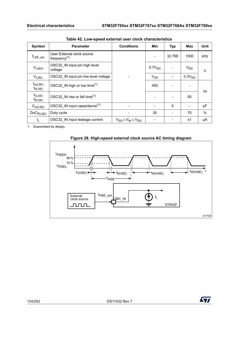
Electrical characteristics STM32F765xx STM32F767xx STM32F768Ax STM32F769xx
134/252 DS11532 Rev 7
Figure 28. High-speed external clock source AC timing diagram
Table 42. Low-speed external user clock characteristics
Symbol Parameter Conditions Min Typ Max Unit
fLSE_extUser External clock source frequency(1)
-
- 32.768 1000 kHz
VLSEHOSC32_IN input pin high level voltage
0.7VDD - VDDV
VLSEL OSC32_IN input pin low level voltage VSS - 0.3VDD
tw(LSE)tf(LSE)
OSC32_IN high or low time(1) 450 - -
nstr(LSE)tf(LSE)
OSC32_IN rise or fall time(1) - - 50
Cin(LSE) OSC32_IN input capacitance(1) - - 5 - pF
DuCy(LSE) Duty cycle - 30 - 70 %
IL OSC32_IN Input leakage current VSS ≤ VIN ≤ VDD - - ±1 µA
1. Guaranteed by design.
ai17528
OSC_INExternal
STM32F
clock source
VHSEH
tf(HSE) tW(HSE)
IL
90 %10 %
THSE
ttr(HSE) tW(HSE)
fHSE_ext
VHSEL
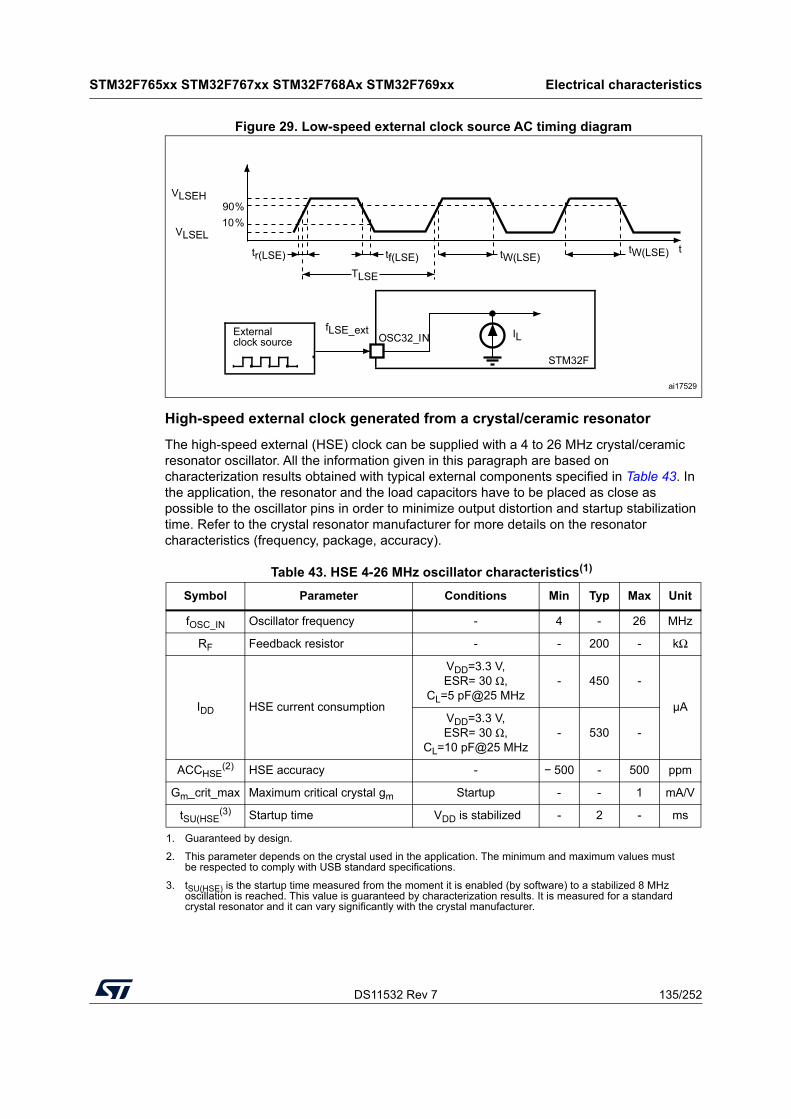
DS11532 Rev 7 135/252
STM32F765xx STM32F767xx STM32F768Ax STM32F769xx Electrical characteristics
218
Figure 29. Low-speed external clock source AC timing diagram
High-speed external clock generated from a crystal/ceramic resonator
The high-speed external (HSE) clock can be supplied with a 4 to 26 MHz crystal/ceramic resonator oscillator. All the information given in this paragraph are based on characterization results obtained with typical external components specified in Table 43. In the application, the resonator and the load capacitors have to be placed as close as possible to the oscillator pins in order to minimize output distortion and startup stabilization time. Refer to the crystal resonator manufacturer for more details on the resonator characteristics (frequency, package, accuracy).
Table 43. HSE 4-26 MHz oscillator characteristics(1)
1. Guaranteed by design.
Symbol Parameter Conditions Min Typ Max Unit
fOSC_IN Oscillator frequency - 4 - 26 MHz
RF Feedback resistor - - 200 - kΩ
IDD HSE current consumption
VDD=3.3 V, ESR= 30 Ω,
CL=5 pF@25 MHz- 450 -
µAVDD=3.3 V, ESR= 30 Ω,
CL=10 pF@25 MHz- 530 -
ACCHSE(2)
2. This parameter depends on the crystal used in the application. The minimum and maximum values must be respected to comply with USB standard specifications.
HSE accuracy - − 500 - 500 ppm
Gm_crit_max Maximum critical crystal gm Startup - - 1 mA/V
tSU(HSE(3)
3. tSU(HSE) is the startup time measured from the moment it is enabled (by software) to a stabilized 8 MHz oscillation is reached. This value is guaranteed by characterization results. It is measured for a standard crystal resonator and it can vary significantly with the crystal manufacturer.
Startup time VDD is stabilized - 2 - ms
ai17529
OSC32_INExternal
STM32F
clock source
VLSEH
tf(LSE) tW(LSE)
IL
90%10%
TLSE
ttr(LSE) tW(LSE)
fLSE_ext
VLSEL
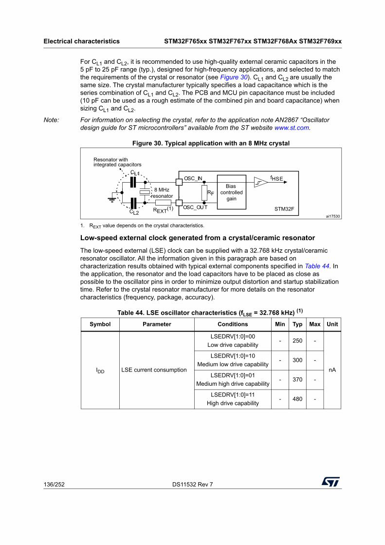
Electrical characteristics STM32F765xx STM32F767xx STM32F768Ax STM32F769xx
136/252 DS11532 Rev 7
For CL1 and CL2, it is recommended to use high-quality external ceramic capacitors in the 5 pF to 25 pF range (typ.), designed for high-frequency applications, and selected to match the requirements of the crystal or resonator (see Figure 30). CL1 and CL2 are usually the same size. The crystal manufacturer typically specifies a load capacitance which is the series combination of CL1 and CL2. The PCB and MCU pin capacitance must be included (10 pF can be used as a rough estimate of the combined pin and board capacitance) when sizing CL1 and CL2.
Note: For information on selecting the crystal, refer to the application note AN2867 “Oscillator design guide for ST microcontrollers” available from the ST website www.st.com.
Figure 30. Typical application with an 8 MHz crystal
1. REXT value depends on the crystal characteristics.
Low-speed external clock generated from a crystal/ceramic resonator
The low-speed external (LSE) clock can be supplied with a 32.768 kHz crystal/ceramic resonator oscillator. All the information given in this paragraph are based on characterization results obtained with typical external components specified in Table 44. In the application, the resonator and the load capacitors have to be placed as close as possible to the oscillator pins in order to minimize output distortion and startup stabilization time. Refer to the crystal resonator manufacturer for more details on the resonator characteristics (frequency, package, accuracy).
Table 44. LSE oscillator characteristics (fLSE = 32.768 kHz) (1)
Symbol Parameter Conditions Min Typ Max Unit
IDD LSE current consumption
LSEDRV[1:0]=00
Low drive capability- 250 -
nA
LSEDRV[1:0]=10
Medium low drive capability- 300 -
LSEDRV[1:0]=01
Medium high drive capability- 370 -
LSEDRV[1:0]=11
High drive capability- 480 -
ai17530
OSC_OUT
OSC_IN fHSECL1
RF
STM32F
8 MHzresonator
Resonator withintegrated capacitors
Bias controlled
gain
REXT(1) CL2
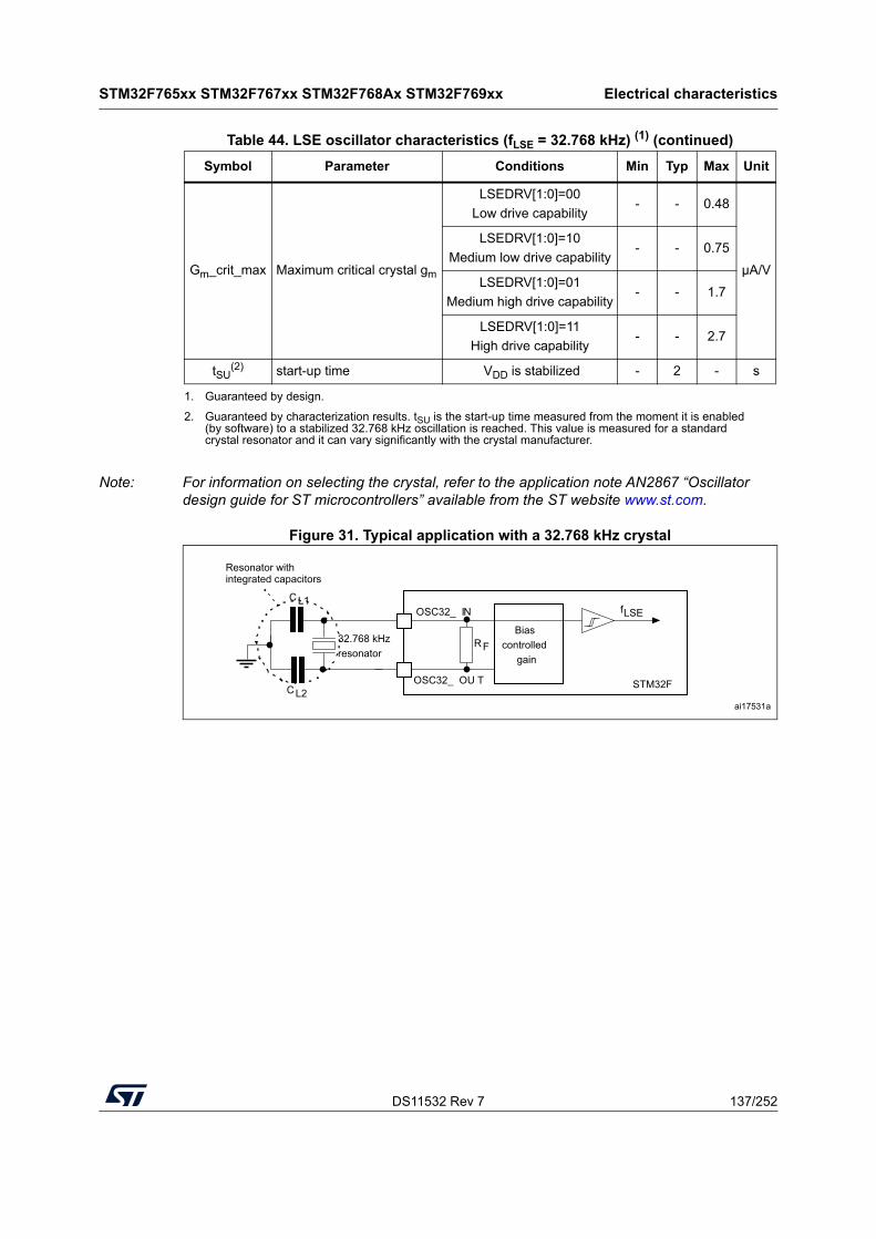
DS11532 Rev 7 137/252
STM32F765xx STM32F767xx STM32F768Ax STM32F769xx Electrical characteristics
218
Note: For information on selecting the crystal, refer to the application note AN2867 “Oscillator design guide for ST microcontrollers” available from the ST website www.st.com.
Figure 31. Typical application with a 32.768 kHz crystal
Gm_crit_max Maximum critical crystal gm
LSEDRV[1:0]=00
Low drive capability- - 0.48
µA/V
LSEDRV[1:0]=10
Medium low drive capability- - 0.75
LSEDRV[1:0]=01
Medium high drive capability- - 1.7
LSEDRV[1:0]=11
High drive capability- - 2.7
tSU(2) start-up time VDD is stabilized - 2 - s
1. Guaranteed by design.
2. Guaranteed by characterization results. tSU is the start-up time measured from the moment it is enabled (by software) to a stabilized 32.768 kHz oscillation is reached. This value is measured for a standard crystal resonator and it can vary significantly with the crystal manufacturer.
Table 44. LSE oscillator characteristics (fLSE = 32.768 kHz) (1) (continued)
Symbol Parameter Conditions Min Typ Max Unit
ai17531a
OSC32_ OU T
OSC32_ IN fLSECL1
RF
STM32F
32.768 kHzresonator
Resonator withintegrated capacitors
Bias controlled
gain
CL2
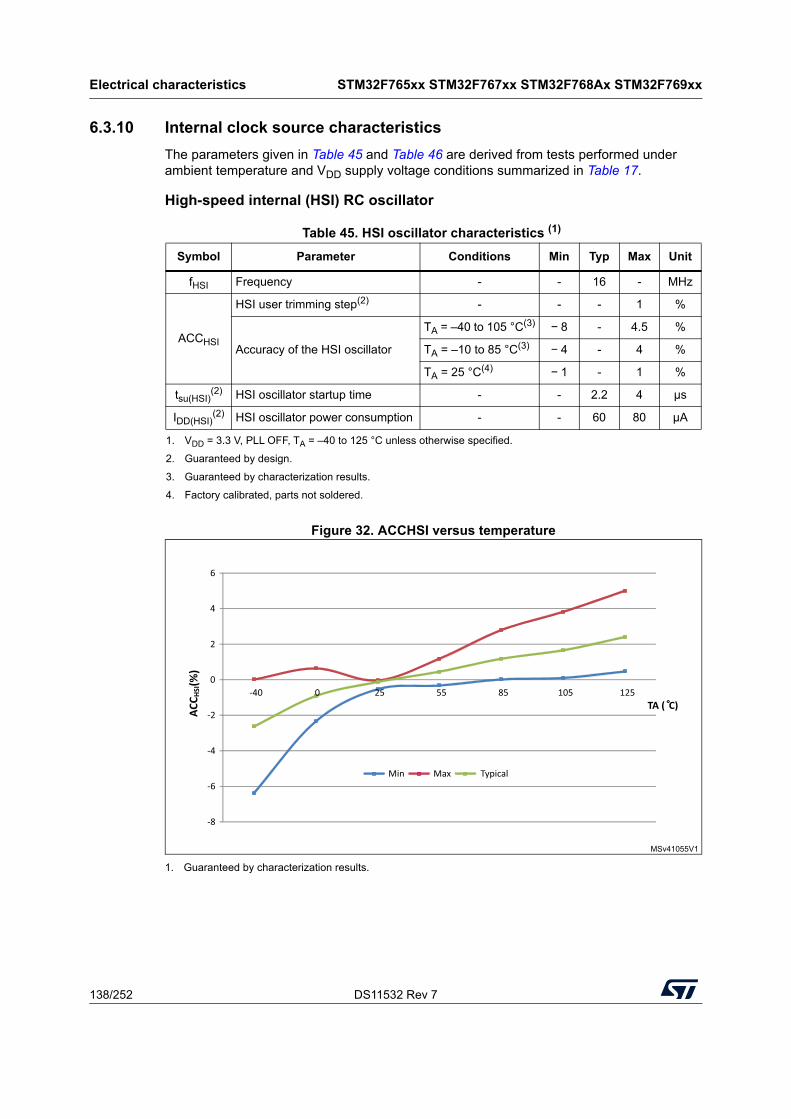
Electrical characteristics STM32F765xx STM32F767xx STM32F768Ax STM32F769xx
138/252 DS11532 Rev 7
6.3.10 Internal clock source characteristics
The parameters given in Table 45 and Table 46 are derived from tests performed under ambient temperature and VDD supply voltage conditions summarized in Table 17.
High-speed internal (HSI) RC oscillator
Figure 32. ACCHSI versus temperature
1. Guaranteed by characterization results.
Table 45. HSI oscillator characteristics (1)
1. VDD = 3.3 V, PLL OFF, TA = –40 to 125 °C unless otherwise specified.
Symbol Parameter Conditions Min Typ Max Unit
fHSI Frequency - - 16 - MHz
ACCHSI
HSI user trimming step(2)
2. Guaranteed by design.
- - - 1 %
Accuracy of the HSI oscillator
TA = –40 to 105 °C(3)
3. Guaranteed by characterization results.
− 8 - 4.5 %
TA = –10 to 85 °C(3) − 4 - 4 %
TA = 25 °C(4)
4. Factory calibrated, parts not soldered.
− 1 - 1 %
tsu(HSI)(2) HSI oscillator startup time - - 2.2 4 µs
IDD(HSI)(2) HSI oscillator power consumption - - 60 80 µA
MSv41055V1
-8
-6
-4
-2
0
2
4
6
-40 0 25 55 85 105 125
ACC H
SI(%
)
TA ( °C)
Min Max Typical
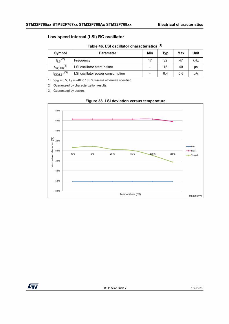
DS11532 Rev 7 139/252
STM32F765xx STM32F767xx STM32F768Ax STM32F769xx Electrical characteristics
218
Low-speed internal (LSI) RC oscillator
Figure 33. LSI deviation versus temperature
Table 46. LSI oscillator characteristics (1)
1. VDD = 3 V, TA = –40 to 105 °C unless otherwise specified.
Symbol Parameter Min Typ Max Unit
fLSI(2)
2. Guaranteed by characterization results.
Frequency 17 32 47 kHz
tsu(LSI)(3)
3. Guaranteed by design.
LSI oscillator startup time - 15 40 µs
IDD(LSI)(3) LSI oscillator power consumption - 0.4 0.6 µA
MS37554V1Temperature (°C)-8.0%
-6.0%
-4.0%
-2.0%
0.0%
2.0%
4.0%
6.0%
8.0%
-40°C 0°C 25°C 85°C 105°C 125°C
Min
Max
Typical
Nor
mal
ized
dev
iatio
n (%
)
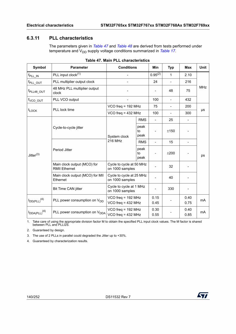
Electrical characteristics STM32F765xx STM32F767xx STM32F768Ax STM32F769xx
140/252 DS11532 Rev 7
6.3.11 PLL characteristics
The parameters given in Table 47 and Table 48 are derived from tests performed under temperature and VDD supply voltage conditions summarized in Table 17.
Table 47. Main PLL characteristics
Symbol Parameter Conditions Min Typ Max Unit
fPLL_IN PLL input clock(1) - 0.95(2) 1 2.10
MHz
fPLL_OUT PLL multiplier output clock - 24 - 216
fPLL48_OUT48 MHz PLL multiplier output clock
- - 48 75
fVCO_OUT PLL VCO output - 100 - 432
tLOCK PLL lock timeVCO freq = 192 MHz 75 - 200
µsVCO freq = 432 MHz 100 - 300
Jitter(3)
Cycle-to-cycle jitter
System clock 216 MHz
RMS - 25 -
ps
peak to peak
- ±150 -
Period Jitter
RMS - 15 -
peak to peak
- ±200 -
Main clock output (MCO) for RMII Ethernet
Cycle to cycle at 50 MHz on 1000 samples
- 32 -
Main clock output (MCO) for MII Ethernet
Cycle to cycle at 25 MHz on 1000 samples
- 40 -
Bit Time CAN jitterCycle to cycle at 1 MHz on 1000 samples
- 330 -
IDD(PLL)(4) PLL power consumption on VDD
VCO freq = 192 MHz
VCO freq = 432 MHz
0.15
0.45-
0.40
0.75mA
IDDA(PLL)(4) PLL power consumption on VDDA
VCO freq = 192 MHz
VCO freq = 432 MHz
0.30
0.55-
0.40
0.85mA
1. Take care of using the appropriate division factor M to obtain the specified PLL input clock values. The M factor is shared between PLL and PLLI2S.
2. Guaranteed by design.
3. The use of 2 PLLs in parallel could degraded the Jitter up to +30%.
4. Guaranteed by characterization results.
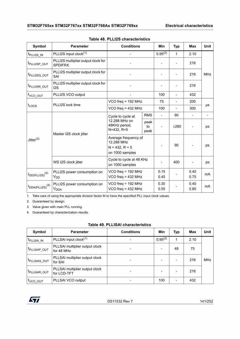
DS11532 Rev 7 141/252
STM32F765xx STM32F767xx STM32F768Ax STM32F769xx Electrical characteristics
218
Table 48. PLLI2S characteristics
Symbol Parameter Conditions Min Typ Max Unit
fPLLI2S_IN PLLI2S input clock(1) - 0.95(2) 1 2.10
MHz
fPLLI2SP_OUTPLLI2S multiplier output clock for SPDIFRX
- - - 216
fPLLI2SQ_OUTPLLI2S multiplier output clock for SAI
- - - 216
fPLLI2SR_OUTPLLI2S multiplier output clock for I2S
- - - 216
fVCO_OUT PLLI2S VCO output - 100 - 432
tLOCK PLLI2S lock timeVCO freq = 192 MHz 75 - 200
µsVCO freq = 432 MHz 100 - 300
Jitter(3)
Master I2S clock jitter
Cycle to cycle at 12.288 MHz on 48KHz period, N=432, R=5
RMS - 90 - -
peak to
peak- ±280 - ps
Average frequency of 12.288 MHz
N = 432, R = 5
on 1000 samples
- 90 - ps
WS I2S clock jitterCycle to cycle at 48 KHz
on 1000 samples- 400 - ps
IDD(PLLI2S)(4) PLLI2S power consumption on
VDD
VCO freq = 192 MHz
VCO freq = 432 MHz
0.15
0.45-
0.40
0.75mA
IDDA(PLLI2S)(4) PLLI2S power consumption on
VDDA
VCO freq = 192 MHz
VCO freq = 432 MHz
0.30
0.55-
0.40
0.85mA
1. Take care of using the appropriate division factor M to have the specified PLL input clock values.
2. Guaranteed by design.
3. Value given with main PLL running.
4. Guaranteed by characterization results.
Table 49. PLLISAI characteristics
Symbol Parameter Conditions Min Typ Max Unit
fPLLSAI_IN PLLSAI input clock(1) - 0.95(2) 1 2.10
MHz
fPLLSAIP_OUTPLLSAI multiplier output clock for 48 MHz
- - 48 75
fPLLSAIQ_OUTPLLSAI multiplier output clock for SAI
- - - 216
fPLLSAIR_OUTPLLSAI multiplier output clock for LCD-TFT
- - - 216
fVCO_OUT PLLSAI VCO output - 100 - 432
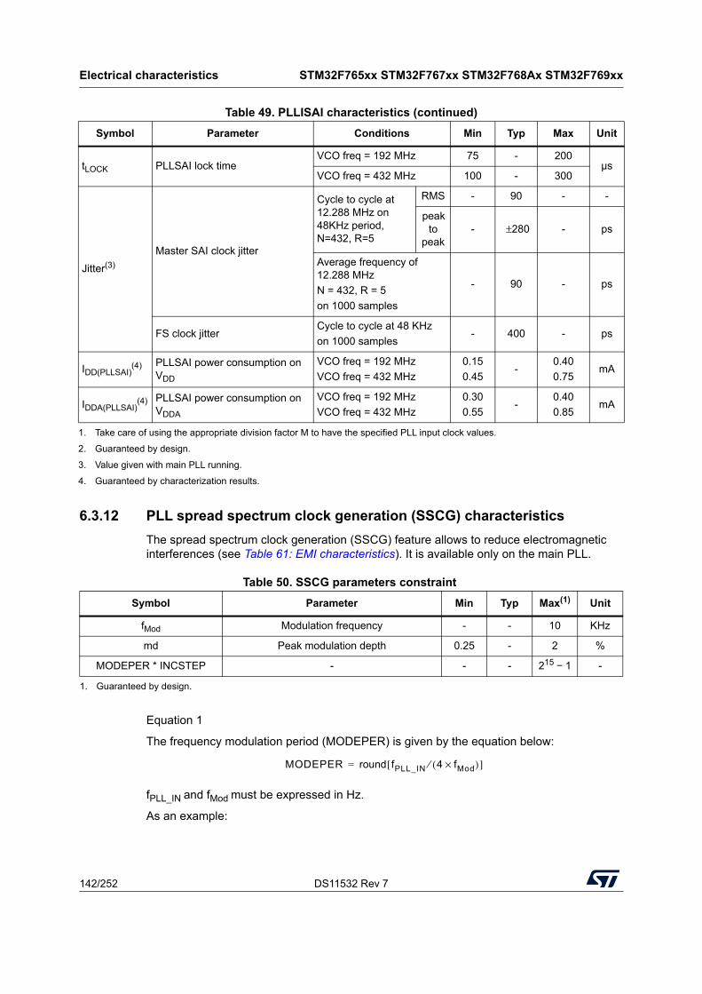
Electrical characteristics STM32F765xx STM32F767xx STM32F768Ax STM32F769xx
142/252 DS11532 Rev 7
6.3.12 PLL spread spectrum clock generation (SSCG) characteristics
The spread spectrum clock generation (SSCG) feature allows to reduce electromagnetic interferences (see Table 61: EMI characteristics). It is available only on the main PLL.
Equation 1
The frequency modulation period (MODEPER) is given by the equation below:
fPLL_IN and fMod must be expressed in Hz.
As an example:
tLOCK PLLSAI lock timeVCO freq = 192 MHz 75 - 200
µsVCO freq = 432 MHz 100 - 300
Jitter(3)
Master SAI clock jitter
Cycle to cycle at 12.288 MHz on 48KHz period, N=432, R=5
RMS - 90 - -
peak to
peak- ±280 - ps
Average frequency of 12.288 MHz
N = 432, R = 5
on 1000 samples
- 90 - ps
FS clock jitterCycle to cycle at 48 KHz
on 1000 samples- 400 - ps
IDD(PLLSAI)(4) PLLSAI power consumption on
VDD
VCO freq = 192 MHz
VCO freq = 432 MHz
0.15
0.45-
0.40
0.75mA
IDDA(PLLSAI)(4) PLLSAI power consumption on
VDDA
VCO freq = 192 MHz
VCO freq = 432 MHz
0.30
0.55-
0.40
0.85mA
1. Take care of using the appropriate division factor M to have the specified PLL input clock values.
2. Guaranteed by design.
3. Value given with main PLL running.
4. Guaranteed by characterization results.
Table 49. PLLISAI characteristics (continued)
Symbol Parameter Conditions Min Typ Max Unit
Table 50. SSCG parameters constraint
Symbol Parameter Min Typ Max(1) Unit
fMod Modulation frequency - - 10 KHz
md Peak modulation depth 0.25 - 2 %
MODEPER * INCSTEP - - - 215 − 1 -
1. Guaranteed by design.
MODEPER round fPLL_IN 4 fMod×( )⁄[ ]=
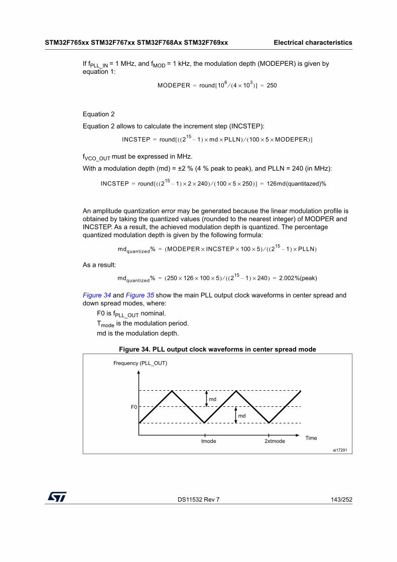
DS11532 Rev 7 143/252
STM32F765xx STM32F767xx STM32F768Ax STM32F769xx Electrical characteristics
218
If fPLL_IN = 1 MHz, and fMOD = 1 kHz, the modulation depth (MODEPER) is given by equation 1:
Equation 2
Equation 2 allows to calculate the increment step (INCSTEP):
fVCO_OUT must be expressed in MHz.
With a modulation depth (md) = ±2 % (4 % peak to peak), and PLLN = 240 (in MHz):
An amplitude quantization error may be generated because the linear modulation profile is obtained by taking the quantized values (rounded to the nearest integer) of MODPER and INCSTEP. As a result, the achieved modulation depth is quantized. The percentage quantized modulation depth is given by the following formula:
As a result:
Figure 34 and Figure 35 show the main PLL output clock waveforms in center spread and down spread modes, where:
F0 is fPLL_OUT nominal.
Tmode is the modulation period.
md is the modulation depth.
Figure 34. PLL output clock waveforms in center spread mode
MODEPER round 106
4 103×( )⁄[ ] 250= =
INCSTEP round 215
1–( ) md PLLN××( ) 100 5× MODEPER×( )⁄[ ]=
INCSTEP round 215
1–( ) 2 240××( ) 100 5× 250×( )⁄[ ] 126md(quantitazed)%= =
mdquantized% MODEPER INCSTEP× 100× 5×( ) 215
1–( ) PLLN×( )⁄=
mdquantized% 250 126× 100× 5×( ) 215
1–( ) 240×( )⁄ 2.002%(peak)= =
Frequency (PLL_OUT)
Time
F0
tmode 2xtmode
md
ai17291
md
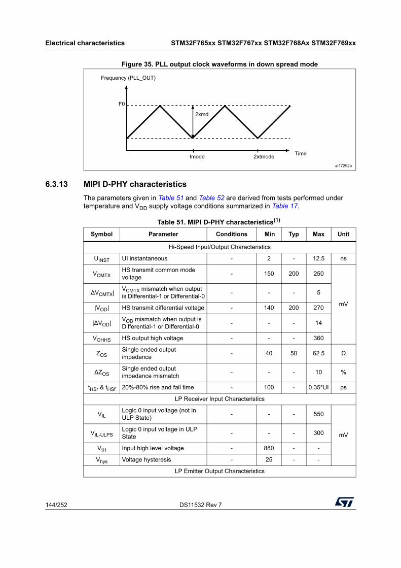
Electrical characteristics STM32F765xx STM32F767xx STM32F768Ax STM32F769xx
144/252 DS11532 Rev 7
Figure 35. PLL output clock waveforms in down spread mode
6.3.13 MIPI D-PHY characteristics
The parameters given in Table 51 and Table 52 are derived from tests performed under temperature and VDD supply voltage conditions summarized in Table 17.
Frequency (PLL_OUT)
Time
F0
tmode 2xtmode
2xmd
ai17292b
Table 51. MIPI D-PHY characteristics(1)
Symbol Parameter Conditions Min Typ Max Unit
Hi-Speed Input/Output Characteristics
UINST UI instantaneous - 2 - 12.5 ns
VCMTXHS transmit common mode voltage
- 150 200 250
mV
|∆VCMTX|VCMTX mismatch when output is Differential-1 or Differential-0
- - - 5
|VOD| HS transmit differential voltage - 140 200 270
|∆VOD|VOD mismatch when output is Differential-1 or Differential-0
- - - 14
VOHHS HS output high voltage - - - 360
ZOSSingle ended output impedance
- 40 50 62.5 Ω
∆ZOSSingle ended output impedance mismatch
- - - 10 %
tHSr & tHSf 20%-80% rise and fall time - 100 - 0.35*UI ps
LP Receiver Input Characteristics
VILLogic 0 input voltage (not in ULP State)
- - - 550
mVVIL-ULPSLogic 0 input voltage in ULP State
- - - 300
VIH Input high level voltage - 880 - -
Vhys Voltage hysteresis - 25 - -
LP Emitter Output Characteristics
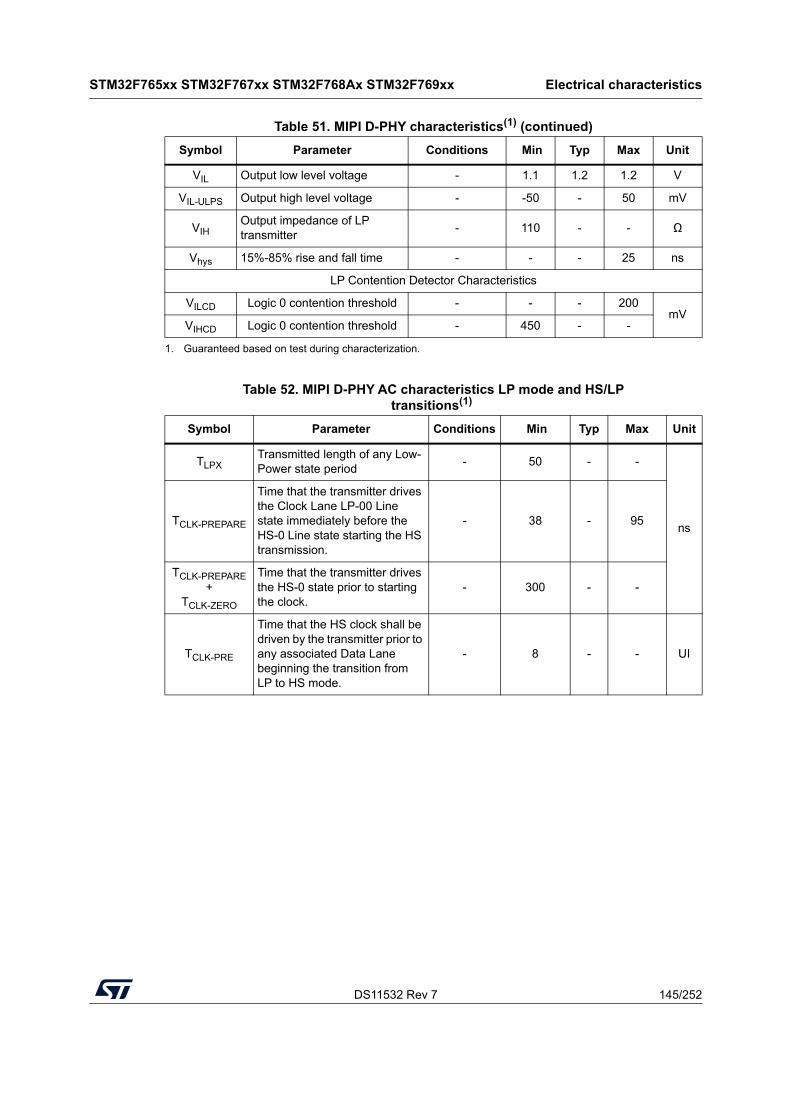
DS11532 Rev 7 145/252
STM32F765xx STM32F767xx STM32F768Ax STM32F769xx Electrical characteristics
218
VIL Output low level voltage - 1.1 1.2 1.2 V
VIL-ULPS Output high level voltage - -50 - 50 mV
VIHOutput impedance of LP transmitter
- 110 - - Ω
Vhys 15%-85% rise and fall time - - - 25 ns
LP Contention Detector Characteristics
VILCD Logic 0 contention threshold - - - 200mV
VIHCD Logic 0 contention threshold - 450 - -
1. Guaranteed based on test during characterization.
Table 52. MIPI D-PHY AC characteristics LP mode and HS/LP transitions(1)
Symbol Parameter Conditions Min Typ Max Unit
TLPXTransmitted length of any Low-Power state period
- 50 - -
nsTCLK-PREPARE
Time that the transmitter drives the Clock Lane LP-00 Line state immediately before the HS-0 Line state starting the HS transmission.
- 38 - 95
TCLK-PREPARE+
TCLK-ZERO
Time that the transmitter drives the HS-0 state prior to starting the clock.
- 300 - -
TCLK-PRE
Time that the HS clock shall be driven by the transmitter prior to any associated Data Lane beginning the transition from LP to HS mode.
- 8 - - UI
Table 51. MIPI D-PHY characteristics(1) (continued)
Symbol Parameter Conditions Min Typ Max Unit
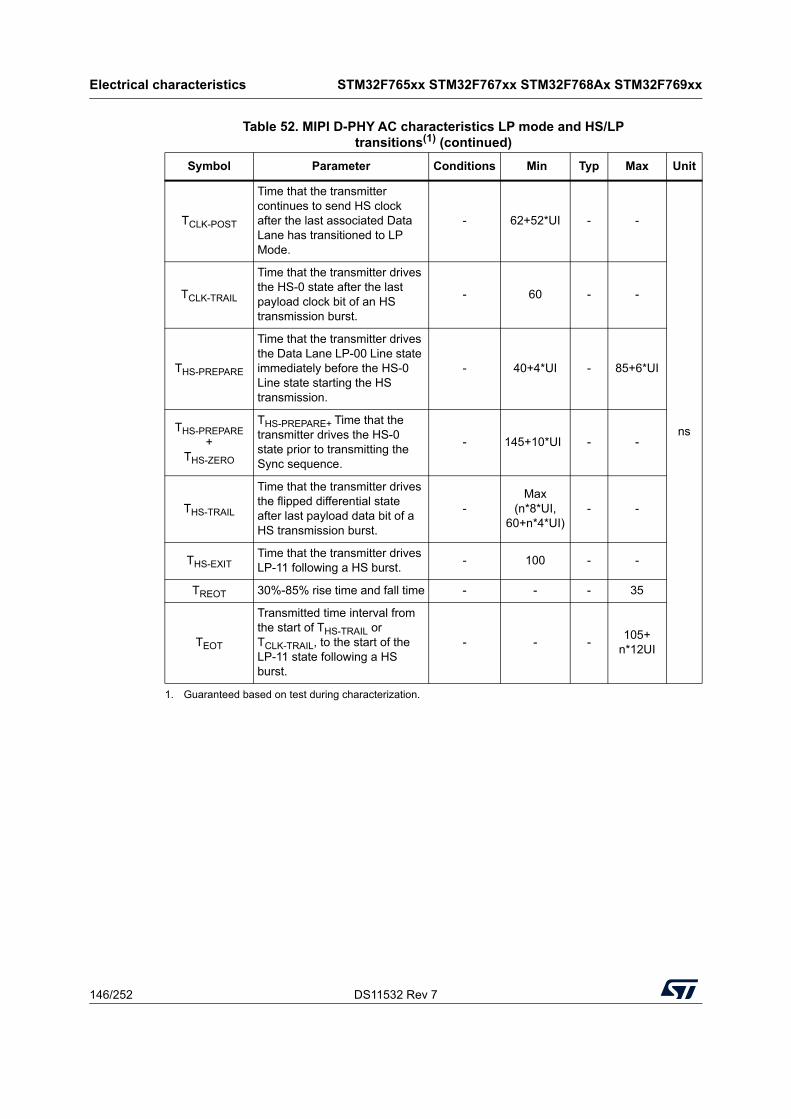
Electrical characteristics STM32F765xx STM32F767xx STM32F768Ax STM32F769xx
146/252 DS11532 Rev 7
TCLK-POST
Time that the transmitter continues to send HS clock after the last associated Data Lane has transitioned to LP Mode.
- 62+52*UI - -
ns
TCLK-TRAIL
Time that the transmitter drives the HS-0 state after the last payload clock bit of an HS transmission burst.
- 60 - -
THS-PREPARE
Time that the transmitter drives the Data Lane LP-00 Line state immediately before the HS-0 Line state starting the HS transmission.
- 40+4*UI - 85+6*UI
THS-PREPARE+
THS-ZERO
THS-PREPARE+ Time that the transmitter drives the HS-0 state prior to transmitting the Sync sequence.
- 145+10*UI - -
THS-TRAIL
Time that the transmitter drives the flipped differential state after last payload data bit of a HS transmission burst.
-Max
(n*8*UI,60+n*4*UI)
- -
THS-EXITTime that the transmitter drives LP-11 following a HS burst.
- 100 - -
TREOT 30%-85% rise time and fall time - - - 35
TEOT
Transmitted time interval from the start of THS-TRAIL or TCLK-TRAIL, to the start of the LP-11 state following a HS burst.
- - -105+
n*12UI
1. Guaranteed based on test during characterization.
Table 52. MIPI D-PHY AC characteristics LP mode and HS/LP transitions(1) (continued)
Symbol Parameter Conditions Min Typ Max Unit
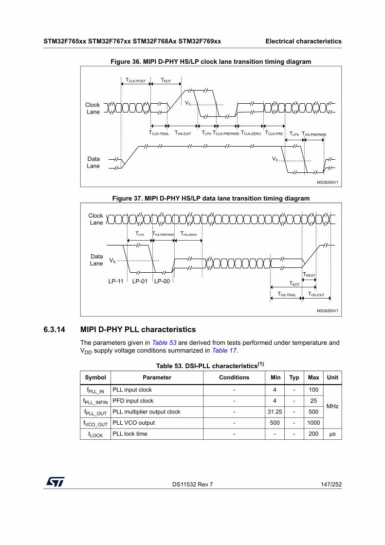
DS11532 Rev 7 147/252
STM32F765xx STM32F767xx STM32F768Ax STM32F769xx Electrical characteristics
218
Figure 36. MIPI D-PHY HS/LP clock lane transition timing diagram
Figure 37. MIPI D-PHY HS/LP data lane transition timing diagram
6.3.14 MIPI D-PHY PLL characteristics
The parameters given in Table 53 are derived from tests performed under temperature and VDD supply voltage conditions summarized in Table 17.
MS38282V1
ClockLane
DataLane
TLPX THS-PREPARETCLK-PRETCLK-ZEROTCLK-PREPARETLPXTHS-EXITTCLK-TRAIL
TCLK-POST
VIL
VIL
TEOT
MS38283V1
ClockLane
THS-PREPARETLPX
THS-TRAIL THS-EXIT
LP-01 LP-00LP-11
DataLane VIL
TREOT
TEOT
THS-ZERO
Table 53. DSI-PLL characteristics(1)
Symbol Parameter Conditions Min Typ Max Unit
fPLL_IN PLL input clock - 4 - 100
MHzfPLL_INFIN PFD input clock - 4 - 25
fPLL_OUT PLL multiplier output clock - 31.25 - 500
fVCO_OUT PLL VCO output - 500 - 1000
tLOCK PLL lock time - - - 200 µs
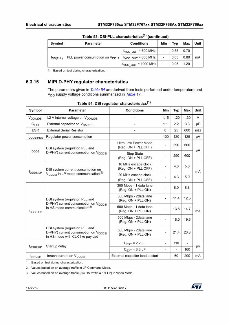
Electrical characteristics STM32F765xx STM32F767xx STM32F768Ax STM32F769xx
148/252 DS11532 Rev 7
6.3.15 MIPI D-PHY regulator characteristics
The parameters given in Table 54 are derived from tests performed under temperature and VDD supply voltage conditions summarized in Table 17.
IDD(PLL) PLL power consumption on VDD12
fVCO_OUT = 500 MHz - 0.55 0.70
mAfVCO_OUT = 600 MHz - 0.65 0.80
fVCO_OUT = 1000 MHz - 0.95 1.20
1. Based on test during characterization.
Table 53. DSI-PLL characteristics(1) (continued)
Symbol Parameter Conditions Min Typ Max Unit
Table 54. DSI regulator characteristics(1)
Symbol Parameter Conditions Min Typ Max Unit
VDD12DSI 1.2 V internal voltage on VDD12DSI - 1.15 1.20 1.30 V
CEXT External capacitor on VCAPDSI - 1.1 2.2 3.3 μF
ESR External Serial Resistor - 0 25 600 mΩ
IDDDSIREG Regulator power consumption - 100 120 125 µA
IDDDSIDSI system (regulator, PLL and D-PHY) current consumption on VDDDSI
Ultra Low Power Mode(Reg. ON + PLL OFF)
- 290 600
µAStop State
(Reg. ON + PLL OFF)- 290 600
IDDDSILPDSI system current consumption on VDDDSI in LP mode communication(2)
10 MHz escape clock(Reg. ON + PLL OFF)
- 4.3 5.0
mA20 MHz escape clock
(Reg. ON + PLL OFF)- 4.3 5.0
IDDDSIHS
DSI system (regulator, PLL and D-PHY) current consumption on VDDDSI in HS mode communication(3)
300 Mbps - 1 data lane(Reg. ON + PLL ON)
- 8.0 8.8
mA
300 Mbps - 2data lane(Reg. ON + PLL ON)
- 11.4 12.5
500 Mbps - 1 data lane(Reg. ON + PLL ON)
- 13.5 14.7
500 Mbps - 2data lane(Reg. ON + PLL ON)
- 18.0 19.6
DSI system (regulator, PLL and D-PHY) current consumption on VDDDSI in HS mode with CLK like payload
500 Mbps - 2data lane(Reg. ON + PLL ON)
- 21.4 23.3
tWAKEUP Startup delayCEXT = 2.2 µF - 110 -
µsCEXT = 3.3 µF - - 160
IINRUSH Inrush current on VDDDSI External capacitor load at start - 60 200 mA
1. Based on test during characterization.
2. Values based on an average traffic in LP Command Mode.
3. Values based on an average traffic (3/4 HS traffic & 1/4 LP) in Video Mode.
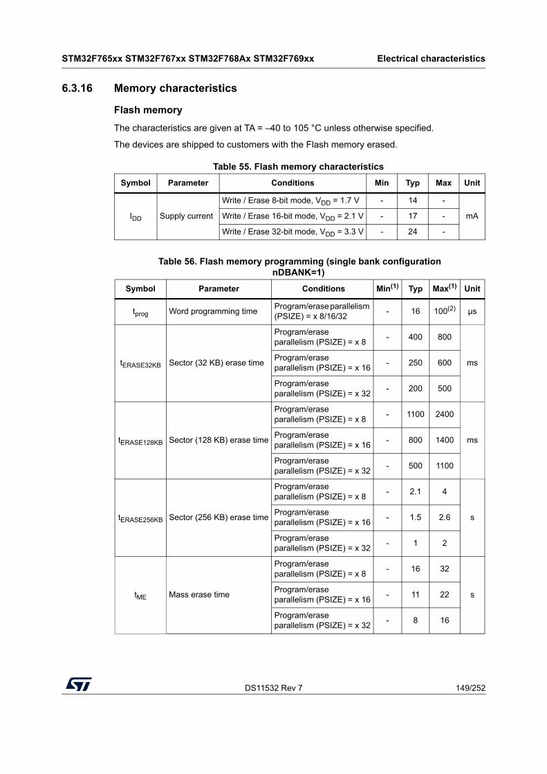
DS11532 Rev 7 149/252
STM32F765xx STM32F767xx STM32F768Ax STM32F769xx Electrical characteristics
218
6.3.16 Memory characteristics
Flash memory
The characteristics are given at TA = –40 to 105 °C unless otherwise specified.
The devices are shipped to customers with the Flash memory erased.
Table 55. Flash memory characteristics
Symbol Parameter Conditions Min Typ Max Unit
IDD Supply current
Write / Erase 8-bit mode, VDD = 1.7 V - 14 -
mAWrite / Erase 16-bit mode, VDD = 2.1 V - 17 -
Write / Erase 32-bit mode, VDD = 3.3 V - 24 -
Table 56. Flash memory programming (single bank configurationnDBANK=1)
Symbol Parameter Conditions Min(1) Typ Max(1) Unit
tprog Word programming timeProgram/erase parallelism (PSIZE) = x 8/16/32
- 16 100(2) µs
tERASE32KB Sector (32 KB) erase time
Program/erase parallelism (PSIZE) = x 8
- 400 800
msProgram/erase parallelism (PSIZE) = x 16
- 250 600
Program/erase parallelism (PSIZE) = x 32
- 200 500
tERASE128KB Sector (128 KB) erase time
Program/erase parallelism (PSIZE) = x 8
- 1100 2400
msProgram/erase parallelism (PSIZE) = x 16
- 800 1400
Program/erase parallelism (PSIZE) = x 32
- 500 1100
tERASE256KB Sector (256 KB) erase time
Program/erase parallelism (PSIZE) = x 8
- 2.1 4
sProgram/erase parallelism (PSIZE) = x 16
- 1.5 2.6
Program/erase parallelism (PSIZE) = x 32
- 1 2
tME Mass erase time
Program/erase parallelism (PSIZE) = x 8
- 16 32
sProgram/erase parallelism (PSIZE) = x 16
- 11 22
Program/erase parallelism (PSIZE) = x 32
- 8 16
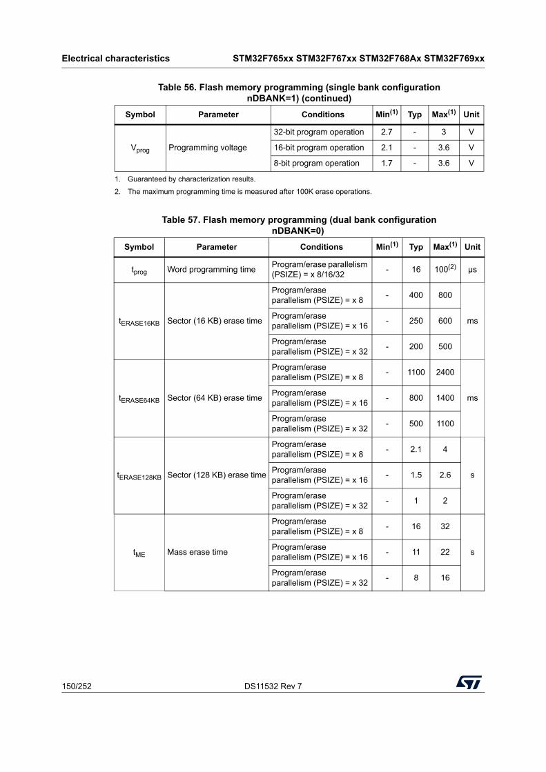
Electrical characteristics STM32F765xx STM32F767xx STM32F768Ax STM32F769xx
150/252 DS11532 Rev 7
Vprog Programming voltage
32-bit program operation 2.7 - 3 V
16-bit program operation 2.1 - 3.6 V
8-bit program operation 1.7 - 3.6 V
1. Guaranteed by characterization results.
2. The maximum programming time is measured after 100K erase operations.
Table 57. Flash memory programming (dual bank configuration nDBANK=0)
Symbol Parameter Conditions Min(1) Typ Max(1) Unit
tprog Word programming timeProgram/erase parallelism (PSIZE) = x 8/16/32
- 16 100(2) µs
tERASE16KB Sector (16 KB) erase time
Program/erase parallelism (PSIZE) = x 8
- 400 800
msProgram/erase parallelism (PSIZE) = x 16
- 250 600
Program/erase parallelism (PSIZE) = x 32
- 200 500
tERASE64KB Sector (64 KB) erase time
Program/erase parallelism (PSIZE) = x 8
- 1100 2400
msProgram/erase parallelism (PSIZE) = x 16
- 800 1400
Program/erase parallelism (PSIZE) = x 32
- 500 1100
tERASE128KB Sector (128 KB) erase time
Program/erase parallelism (PSIZE) = x 8
- 2.1 4
sProgram/erase parallelism (PSIZE) = x 16
- 1.5 2.6
Program/erase parallelism (PSIZE) = x 32
- 1 2
tME Mass erase time
Program/erase parallelism (PSIZE) = x 8
- 16 32
sProgram/erase parallelism (PSIZE) = x 16
- 11 22
Program/erase parallelism (PSIZE) = x 32
- 8 16
Table 56. Flash memory programming (single bank configurationnDBANK=1) (continued)
Symbol Parameter Conditions Min(1) Typ Max(1) Unit
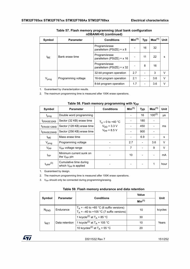
DS11532 Rev 7 151/252
STM32F765xx STM32F767xx STM32F768Ax STM32F769xx Electrical characteristics
218
tBE Bank erase time
Program/erase parallelism (PSIZE) = x 8
- 16 32
sProgram/erase parallelism (PSIZE) = x 16
- 11 22
Program/erase parallelism (PSIZE) = x 32
- 8 16
Vprog Programming voltage
32-bit program operation 2.7 - 3 V
16-bit program operation 2.1 - 3.6 V
8-bit program operation 1.7 - 3.6 V
1. Guaranteed by characterization results.
2. The maximum programming time is measured after 100K erase operations.
Table 58. Flash memory programming with VPP
Symbol Parameter Conditions Min(1) Typ Max(1)
1. Guaranteed by design.
Unit
tprog Double word programming
TA = 0 to +40 °C
VDD = 3.3 V
VPP = 8.5 V
- 16 100(2)
2. The maximum programming time is measured after 100K erase operations.
µs
tERASE32KB Sector (32 KB) erase time - 180 -
mstERASE128KB Sector (128 KB) erase time - 450 -
tERASE256KB Sector (256 KB) erase time - 900 -
tME Mass erase time - 6.9 - s
Vprog Programming voltage - 2.7 - 3.6 V
VPP VPP voltage range - 7 - 9 V
IPPMinimum current sunk on the VPP pin
- 10 - - mA
tVPP(3)
3. VPP should only be connected during programming/erasing.
Cumulative time during which VPP is applied
- - - 1 hour
Table 59. Flash memory endurance and data retention
Symbol Parameter ConditionsValue
UnitMin(1)
NEND EnduranceTA = –40 to +85 °C (6 suffix versions)
TA = –40 to +105 °C (7 suffix versions)10 kcycles
tRET Data retention
1 kcycle(2) at TA = 85 °C 30
Years1 kcycle(2) at TA = 105 °C 10
10 kcycles(2) at TA = 55 °C 20
Table 57. Flash memory programming (dual bank configuration nDBANK=0) (continued)
Symbol Parameter Conditions Min(1) Typ Max(1) Unit
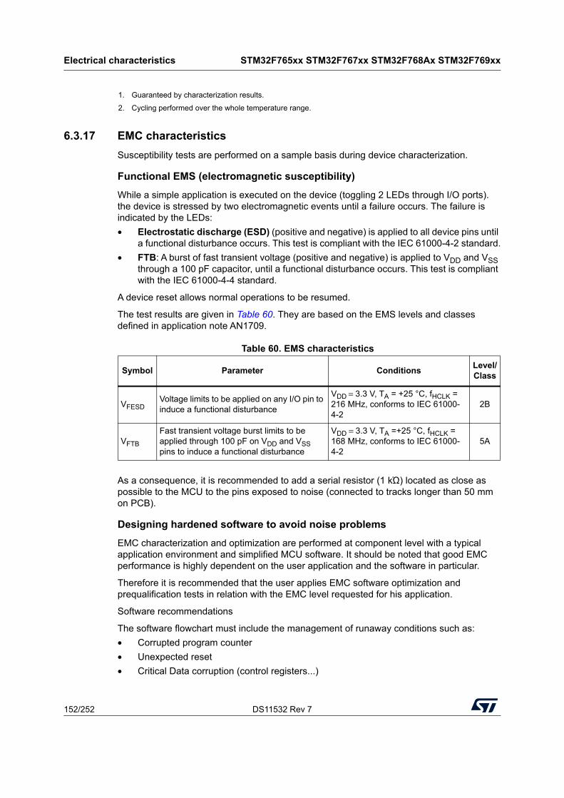
Electrical characteristics STM32F765xx STM32F767xx STM32F768Ax STM32F769xx
152/252 DS11532 Rev 7
6.3.17 EMC characteristics
Susceptibility tests are performed on a sample basis during device characterization.
Functional EMS (electromagnetic susceptibility)
While a simple application is executed on the device (toggling 2 LEDs through I/O ports). the device is stressed by two electromagnetic events until a failure occurs. The failure is indicated by the LEDs:
• Electrostatic discharge (ESD) (positive and negative) is applied to all device pins until a functional disturbance occurs. This test is compliant with the IEC 61000-4-2 standard.
• FTB: A burst of fast transient voltage (positive and negative) is applied to VDD and VSS through a 100 pF capacitor, until a functional disturbance occurs. This test is compliant with the IEC 61000-4-4 standard.
A device reset allows normal operations to be resumed.
The test results are given in Table 60. They are based on the EMS levels and classes defined in application note AN1709.
As a consequence, it is recommended to add a serial resistor (1 kΏ) located as close as possible to the MCU to the pins exposed to noise (connected to tracks longer than 50 mm on PCB).
Designing hardened software to avoid noise problems
EMC characterization and optimization are performed at component level with a typical application environment and simplified MCU software. It should be noted that good EMC performance is highly dependent on the user application and the software in particular.
Therefore it is recommended that the user applies EMC software optimization and prequalification tests in relation with the EMC level requested for his application.
Software recommendations
The software flowchart must include the management of runaway conditions such as:
• Corrupted program counter
• Unexpected reset
• Critical Data corruption (control registers...)
1. Guaranteed by characterization results.
2. Cycling performed over the whole temperature range.
Table 60. EMS characteristics
Symbol Parameter ConditionsLevel/Class
VFESDVoltage limits to be applied on any I/O pin to induce a functional disturbance
VDD = 3.3 V, TA = +25 °C, fHCLK = 216 MHz, conforms to IEC 61000-4-2
2B
VFTB
Fast transient voltage burst limits to be applied through 100 pF on VDD and VSS pins to induce a functional disturbance
VDD = 3.3 V, TA =+25 °C, fHCLK = 168 MHz, conforms to IEC 61000-4-2
5A
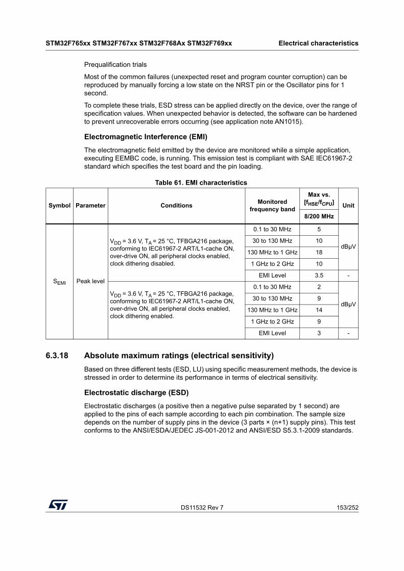
DS11532 Rev 7 153/252
STM32F765xx STM32F767xx STM32F768Ax STM32F769xx Electrical characteristics
218
Prequalification trials
Most of the common failures (unexpected reset and program counter corruption) can be reproduced by manually forcing a low state on the NRST pin or the Oscillator pins for 1 second.
To complete these trials, ESD stress can be applied directly on the device, over the range of specification values. When unexpected behavior is detected, the software can be hardened to prevent unrecoverable errors occurring (see application note AN1015).
Electromagnetic Interference (EMI)
The electromagnetic field emitted by the device are monitored while a simple application, executing EEMBC code, is running. This emission test is compliant with SAE IEC61967-2 standard which specifies the test board and the pin loading.
6.3.18 Absolute maximum ratings (electrical sensitivity)
Based on three different tests (ESD, LU) using specific measurement methods, the device is stressed in order to determine its performance in terms of electrical sensitivity.
Electrostatic discharge (ESD)
Electrostatic discharges (a positive then a negative pulse separated by 1 second) are applied to the pins of each sample according to each pin combination. The sample size depends on the number of supply pins in the device (3 parts × (n+1) supply pins). This test conforms to the ANSI/ESDA/JEDEC JS-001-2012 and ANSI/ESD S5.3.1-2009 standards.
Table 61. EMI characteristics
Symbol Parameter ConditionsMonitored
frequency band
Max vs. [fHSE/fCPU] Unit
8/200 MHz
SEMI Peak level
VDD = 3.6 V, TA = 25 °C, TFBGA216 package, conforming to IEC61967-2 ART/L1-cache ON, over-drive ON, all peripheral clocks enabled, clock dithering disabled.
0.1 to 30 MHz 5
dBµV30 to 130 MHz 10
130 MHz to 1 GHz 18
1 GHz to 2 GHz 10
EMI Level 3.5 -
VDD = 3.6 V, TA = 25 °C, TFBGA216 package, conforming to IEC61967-2 ART/L1-cache ON, over-drive ON, all peripheral clocks enabled, clock dithering enabled.
0.1 to 30 MHz 2
dBµV30 to 130 MHz 9
130 MHz to 1 GHz 14
1 GHz to 2 GHz 9
EMI Level 3 -
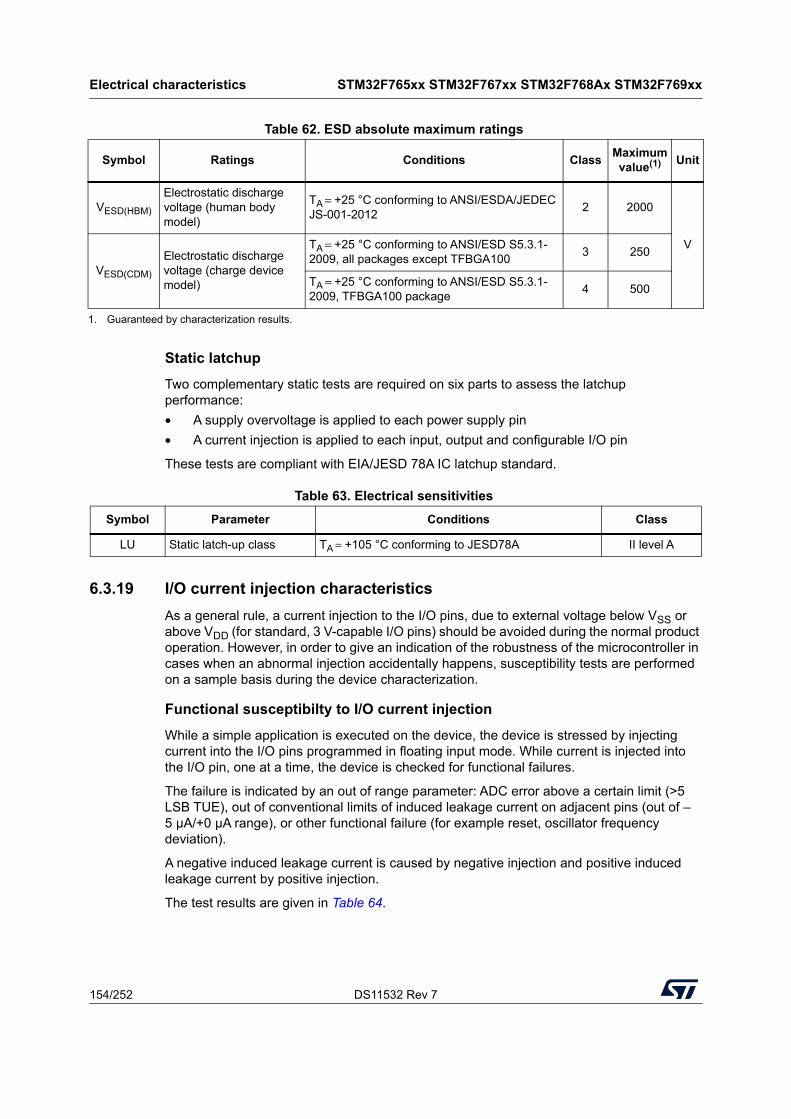
Electrical characteristics STM32F765xx STM32F767xx STM32F768Ax STM32F769xx
154/252 DS11532 Rev 7
Static latchup
Two complementary static tests are required on six parts to assess the latchup performance:
• A supply overvoltage is applied to each power supply pin
• A current injection is applied to each input, output and configurable I/O pin
These tests are compliant with EIA/JESD 78A IC latchup standard.
6.3.19 I/O current injection characteristics
As a general rule, a current injection to the I/O pins, due to external voltage below VSS or above VDD (for standard, 3 V-capable I/O pins) should be avoided during the normal product operation. However, in order to give an indication of the robustness of the microcontroller in cases when an abnormal injection accidentally happens, susceptibility tests are performed on a sample basis during the device characterization.
Functional susceptibilty to I/O current injection
While a simple application is executed on the device, the device is stressed by injecting current into the I/O pins programmed in floating input mode. While current is injected into the I/O pin, one at a time, the device is checked for functional failures.
The failure is indicated by an out of range parameter: ADC error above a certain limit (>5 LSB TUE), out of conventional limits of induced leakage current on adjacent pins (out of –5 µA/+0 µA range), or other functional failure (for example reset, oscillator frequency deviation).
A negative induced leakage current is caused by negative injection and positive induced leakage current by positive injection.
The test results are given in Table 64.
Table 62. ESD absolute maximum ratings
Symbol Ratings Conditions ClassMaximum value(1) Unit
VESD(HBM)
Electrostatic discharge voltage (human body model)
TA = +25 °C conforming to ANSI/ESDA/JEDEC JS-001-2012
2 2000
V
VESD(CDM)
Electrostatic discharge voltage (charge device model)
TA = +25 °C conforming to ANSI/ESD S5.3.1-2009, all packages except TFBGA100
3 250
TA = +25 °C conforming to ANSI/ESD S5.3.1-2009, TFBGA100 package
4 500
1. Guaranteed by characterization results.
Table 63. Electrical sensitivities
Symbol Parameter Conditions Class
LU Static latch-up class TA = +105 °C conforming to JESD78A II level A
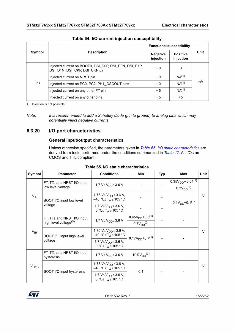
DS11532 Rev 7 155/252
STM32F765xx STM32F767xx STM32F768Ax STM32F769xx Electrical characteristics
218
Note: It is recommended to add a Schottky diode (pin to ground) to analog pins which may potentially inject negative currents.
6.3.20 I/O port characteristics
General input/output characteristics
Unless otherwise specified, the parameters given in Table 65: I/O static characteristics are derived from tests performed under the conditions summarized in Table 17. All I/Os are CMOS and TTL compliant.
Table 64. I/O current injection susceptibility
Symbol Description
Functional susceptibility
UnitNegative injection
Positive injection
IINJ
Injected current on BOOT0, DSI_D0P, DSI_D0N, DSI_D1P, DSI_D1N, DSI_CKP, DSI_CKN pin
− 0 0
mAInjected current on NRST pin − 0 NA(1)
Injected current on PC0, PC2, PH1_OSCOUT pins − 0 NA(1)
Injected current on any other FT pin − 5 NA(1)
Injected current on any other pins − 5 +5
1. Injection is not possible.
Table 65. I/O static characteristics
Symbol Parameter Conditions Min Typ Max Unit
VIL
FT, TTa and NRST I/O input low level voltage
1.7 V≤ VDD≤ 3.6 V - -0.35VDD−0.04(1)
V
0.3VDD(2)
BOOT I/O input low level voltage
1.75 V≤ VDD ≤ 3.6 V, –40 °C≤ TA ≤ 105 °C
- -
0.1VDD+0.1(1)
1.7 V≤ VDD ≤ 3.6 V, 0 °C≤ TA ≤ 105 °C
- -
VIH
FT, TTa and NRST I/O input high level voltage(5) 1.7 V≤ VDD≤ 3.6 V
0.45VDD+0.3(1)
- -
V
0.7VDD(2)
BOOT I/O input high level voltage
1.75 V≤ VDD ≤ 3.6 V, –40 °C≤ TA ≤ 105 °C
0.17VDD+0.7(1) - -1.7 V≤ VDD ≤ 3.6 V, 0 °C≤ TA ≤ 105 °C
VHYS
FT, TTa and NRST I/O input hysteresis
1.7 V≤ VDD≤ 3.6 V 10%VDD(3) - -
V
BOOT I/O input hysteresis
1.75 V≤ VDD ≤ 3.6 V, –40 °C≤ TA ≤ 105 °C
0.1 - -1.7 V≤ VDD ≤ 3.6 V, 0 °C≤ TA ≤ 105 °C
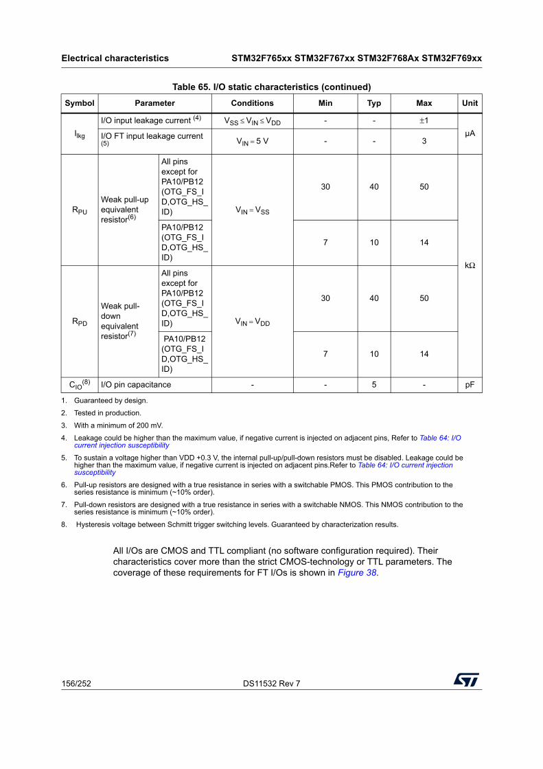
Electrical characteristics STM32F765xx STM32F767xx STM32F768Ax STM32F769xx
156/252 DS11532 Rev 7
All I/Os are CMOS and TTL compliant (no software configuration required). Their characteristics cover more than the strict CMOS-technology or TTL parameters. The coverage of these requirements for FT I/Os is shown in Figure 38.
Ilkg
I/O input leakage current (4) VSS ≤ VIN ≤ VDD - - ±1
µAI/O FT input leakage current (5) VIN = 5 V - - 3
RPU
Weak pull-up equivalent resistor(6)
All pins except for PA10/PB12 (OTG_FS_ID,OTG_HS_ID) VIN = VSS
30 40 50
kΩ
PA10/PB12 (OTG_FS_ID,OTG_HS_ID)
7 10 14
RPD
Weak pull-down equivalent resistor(7)
All pins except for PA10/PB12 (OTG_FS_ID,OTG_HS_ID) VIN = VDD
30 40 50
PA10/PB12 (OTG_FS_ID,OTG_HS_ID)
7 10 14
CIO(8) I/O pin capacitance - - 5 - pF
1. Guaranteed by design.
2. Tested in production.
3. With a minimum of 200 mV.
4. Leakage could be higher than the maximum value, if negative current is injected on adjacent pins, Refer to Table 64: I/O current injection susceptibility
5. To sustain a voltage higher than VDD +0.3 V, the internal pull-up/pull-down resistors must be disabled. Leakage could be higher than the maximum value, if negative current is injected on adjacent pins.Refer to Table 64: I/O current injection susceptibility
6. Pull-up resistors are designed with a true resistance in series with a switchable PMOS. This PMOS contribution to the series resistance is minimum (~10% order).
7. Pull-down resistors are designed with a true resistance in series with a switchable NMOS. This NMOS contribution to the series resistance is minimum (~10% order).
8. Hysteresis voltage between Schmitt trigger switching levels. Guaranteed by characterization results.
Table 65. I/O static characteristics (continued)
Symbol Parameter Conditions Min Typ Max Unit
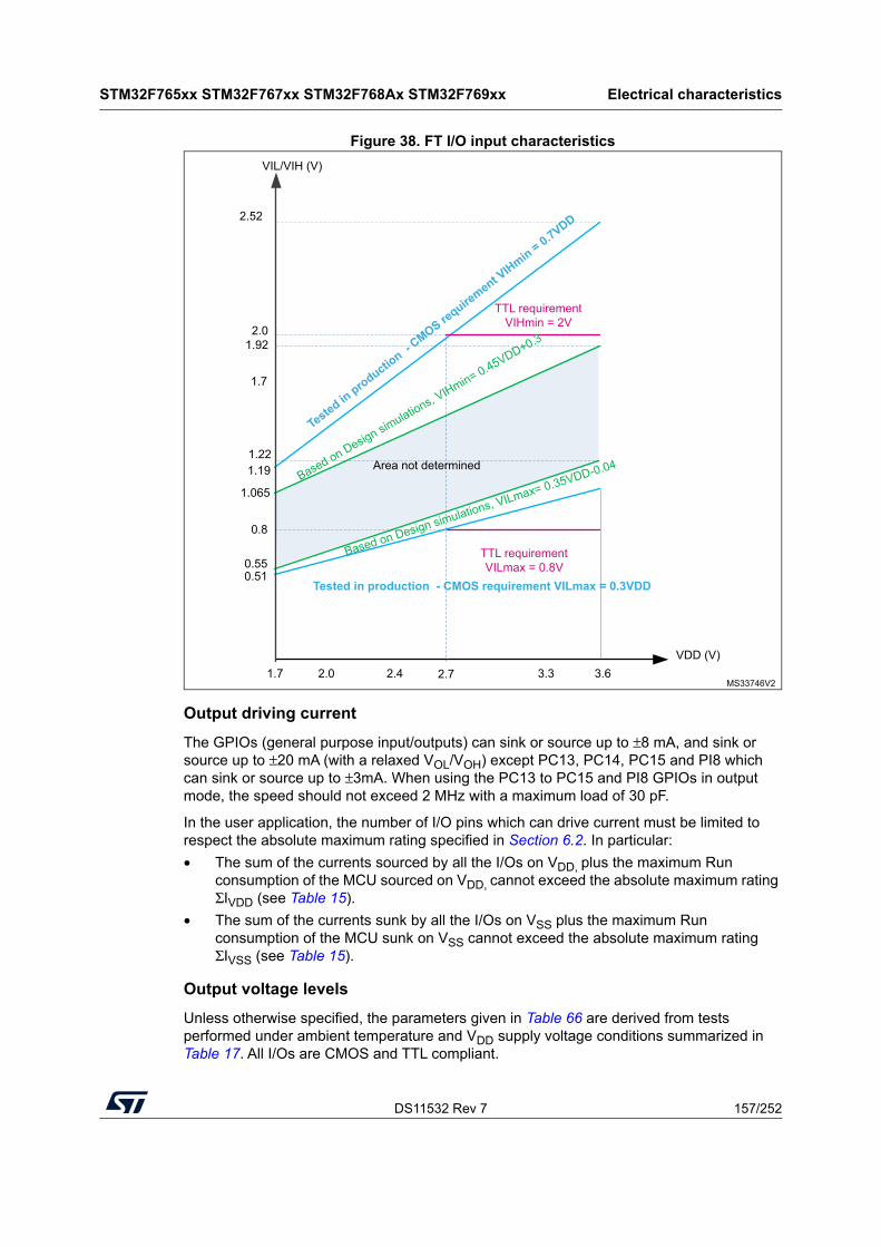
DS11532 Rev 7 157/252
STM32F765xx STM32F767xx STM32F768Ax STM32F769xx Electrical characteristics
218
Figure 38. FT I/O input characteristics
Output driving current
The GPIOs (general purpose input/outputs) can sink or source up to ±8 mA, and sink or source up to ±20 mA (with a relaxed VOL/VOH) except PC13, PC14, PC15 and PI8 which can sink or source up to ±3mA. When using the PC13 to PC15 and PI8 GPIOs in output mode, the speed should not exceed 2 MHz with a maximum load of 30 pF.
In the user application, the number of I/O pins which can drive current must be limited to respect the absolute maximum rating specified in Section 6.2. In particular:
• The sum of the currents sourced by all the I/Os on VDD, plus the maximum Run consumption of the MCU sourced on VDD, cannot exceed the absolute maximum rating ΣIVDD (see Table 15).
• The sum of the currents sunk by all the I/Os on VSS plus the maximum Run consumption of the MCU sunk on VSS cannot exceed the absolute maximum rating ΣIVSS (see Table 15).
Output voltage levels
Unless otherwise specified, the parameters given in Table 66 are derived from tests performed under ambient temperature and VDD supply voltage conditions summarized in Table 17. All I/Os are CMOS and TTL compliant.
MS33746V2
1.92
1.065
1.22
1.7 2.0 2.4 2.7 3.3 3.6
2.0
0.55
0.8
VDD (V)
VIL/VIH (V)
Tested in productio
n - CMOS re
quirement V
IHmin = 0.7VDD
Tested in production - CMOS requirement VILmax = 0.3VDD
Based on Design simulations, VILmax= 0.35VDD-0.04
TTL requirement VIHmin = 2V
TTL requirement VILmax = 0.8V
0.51
2.52
Area not determined1.19
1.7
Based on Design simulations, VIHmin= 0.45VDD+0.3
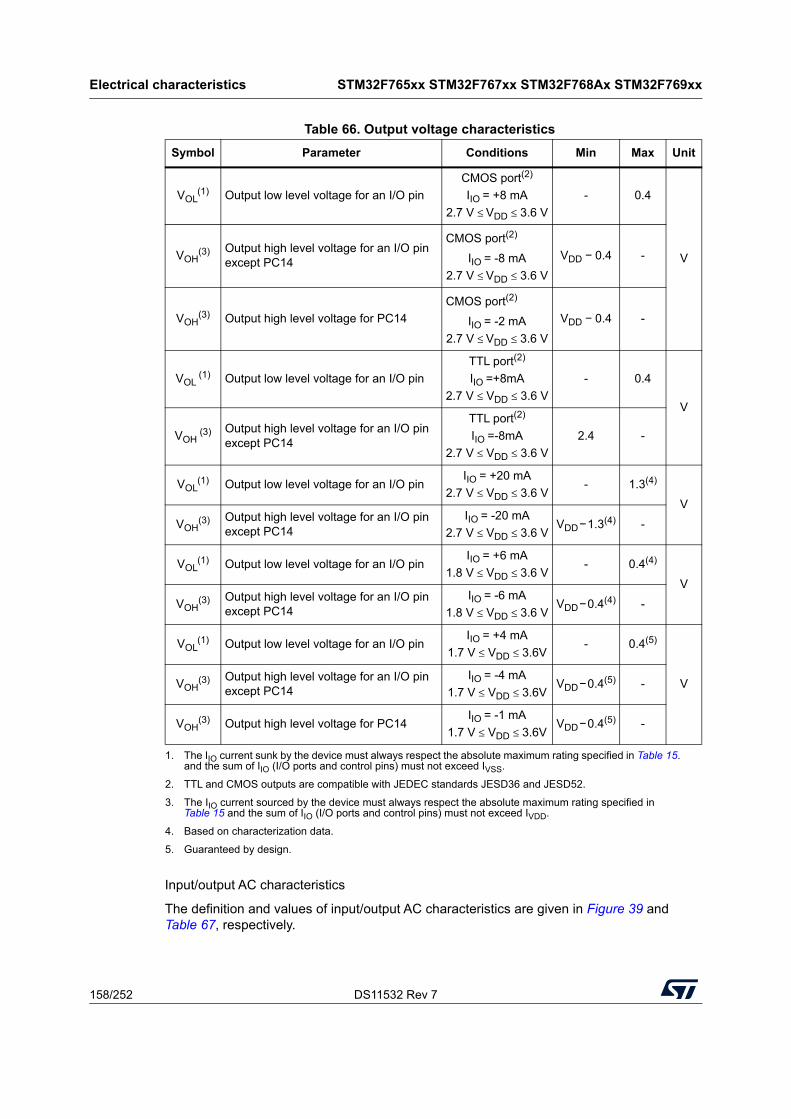
Electrical characteristics STM32F765xx STM32F767xx STM32F768Ax STM32F769xx
158/252 DS11532 Rev 7
Input/output AC characteristics
The definition and values of input/output AC characteristics are given in Figure 39 and Table 67, respectively.
Table 66. Output voltage characteristics
Symbol Parameter Conditions Min Max Unit
VOL(1)
1. The IIO current sunk by the device must always respect the absolute maximum rating specified in Table 15. and the sum of IIO (I/O ports and control pins) must not exceed IVSS.
Output low level voltage for an I/O pin
CMOS port(2)
IIO = +8 mA
2.7 V ≤ VDD ≤ 3.6 V
2. TTL and CMOS outputs are compatible with JEDEC standards JESD36 and JESD52.
- 0.4
VVOH(3)
3. The IIO current sourced by the device must always respect the absolute maximum rating specified in Table 15 and the sum of IIO (I/O ports and control pins) must not exceed IVDD.
Output high level voltage for an I/O pin except PC14
CMOS port(2)
IIO = -8 mA
2.7 V ≤ VDD ≤ 3.6 V
VDD − 0.4 -
VOH(3) Output high level voltage for PC14
CMOS port(2)
IIO = -2 mA
2.7 V ≤ VDD ≤ 3.6 V
VDD − 0.4 -
VOL (1) Output low level voltage for an I/O pin
TTL port(2)
IIO =+8mA
2.7 V ≤ VDD ≤ 3.6 V
- 0.4
V
VOH (3) Output high level voltage for an I/O pin
except PC14
TTL port(2)
IIO =-8mA
2.7 V ≤ VDD ≤ 3.6 V
2.4 -
VOL(1) Output low level voltage for an I/O pin
IIO = +20 mA
2.7 V ≤ VDD ≤ 3.6 V- 1.3(4)
4. Based on characterization data.
V
VOH(3) Output high level voltage for an I/O pin
except PC14IIO = -20 mA
2.7 V ≤ VDD ≤ 3.6 VVDD−1.3(4) -
VOL(1) Output low level voltage for an I/O pin
IIO = +6 mA
1.8 V ≤ VDD ≤ 3.6 V- 0.4(4)
V
VOH(3) Output high level voltage for an I/O pin
except PC14IIO = -6 mA
1.8 V ≤ VDD ≤ 3.6 VVDD−0.4(4) -
VOL(1) Output low level voltage for an I/O pin
IIO = +4 mA
1.7 V ≤ VDD ≤ 3.6V- 0.4(5)
5. Guaranteed by design.
VVOH(3) Output high level voltage for an I/O pin
except PC14IIO = -4 mA
1.7 V ≤ VDD ≤ 3.6VVDD−0.4(5) -
VOH(3) Output high level voltage for PC14
IIO = -1 mA
1.7 V ≤ VDD ≤ 3.6VVDD−0.4(5) -
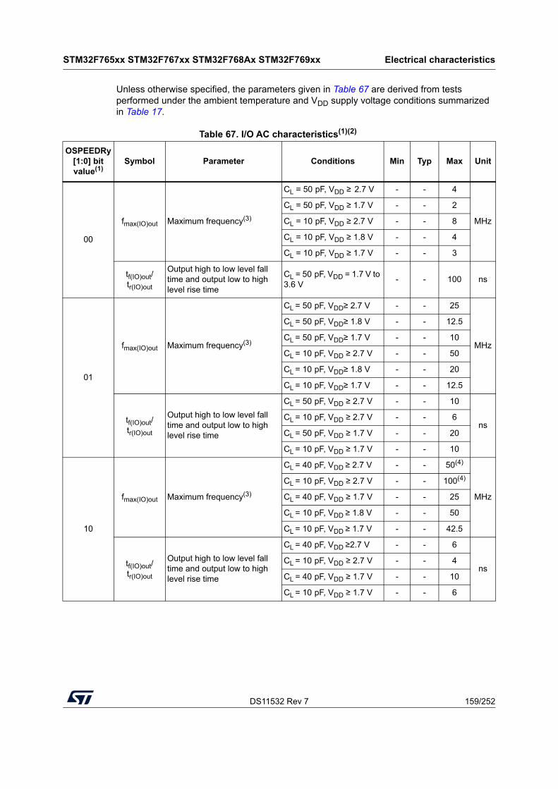
DS11532 Rev 7 159/252
STM32F765xx STM32F767xx STM32F768Ax STM32F769xx Electrical characteristics
218
Unless otherwise specified, the parameters given in Table 67 are derived from tests performed under the ambient temperature and VDD supply voltage conditions summarized in Table 17.
Table 67. I/O AC characteristics(1)(2)
OSPEEDRy[1:0] bit value(1)
Symbol Parameter Conditions Min Typ Max Unit
00
fmax(IO)out Maximum frequency(3)
CL = 50 pF, VDD ≥ 2.7 V - - 4
MHz
CL = 50 pF, VDD ≥ 1.7 V - - 2
CL = 10 pF, VDD ≥ 2.7 V - - 8
CL = 10 pF, VDD ≥ 1.8 V - - 4
CL = 10 pF, VDD ≥ 1.7 V - - 3
tf(IO)out/tr(IO)out
Output high to low level fall time and output low to high level rise time
CL = 50 pF, VDD = 1.7 V to 3.6 V
- - 100 ns
01
fmax(IO)out Maximum frequency(3)
CL = 50 pF, VDD≥ 2.7 V - - 25
MHz
CL = 50 pF, VDD≥ 1.8 V - - 12.5
CL = 50 pF, VDD≥ 1.7 V - - 10
CL = 10 pF, VDD ≥ 2.7 V - - 50
CL = 10 pF, VDD≥ 1.8 V - - 20
CL = 10 pF, VDD≥ 1.7 V - - 12.5
tf(IO)out/tr(IO)out
Output high to low level fall time and output low to high level rise time
CL = 50 pF, VDD ≥ 2.7 V - - 10
nsCL = 10 pF, VDD ≥ 2.7 V - - 6
CL = 50 pF, VDD ≥ 1.7 V - - 20
CL = 10 pF, VDD ≥ 1.7 V - - 10
10
fmax(IO)out Maximum frequency(3)
CL = 40 pF, VDD ≥ 2.7 V - - 50(4)
MHz
CL = 10 pF, VDD ≥ 2.7 V - - 100(4)
CL = 40 pF, VDD ≥ 1.7 V - - 25
CL = 10 pF, VDD ≥ 1.8 V - - 50
CL = 10 pF, VDD ≥ 1.7 V - - 42.5
tf(IO)out/tr(IO)out
Output high to low level fall time and output low to high level rise time
CL = 40 pF, VDD ≥2.7 V - - 6
nsCL = 10 pF, VDD ≥ 2.7 V - - 4
CL = 40 pF, VDD ≥ 1.7 V - - 10
CL = 10 pF, VDD ≥ 1.7 V - - 6
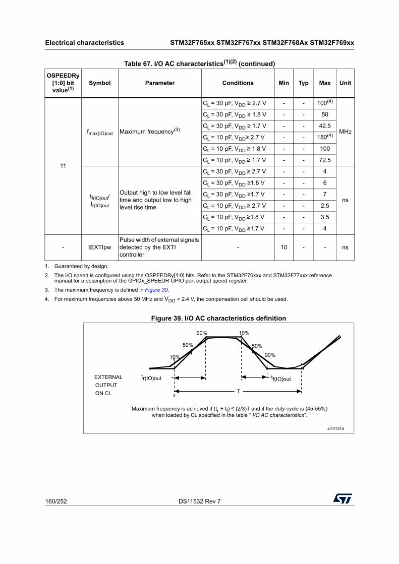
Electrical characteristics STM32F765xx STM32F767xx STM32F768Ax STM32F769xx
160/252 DS11532 Rev 7
Figure 39. I/O AC characteristics definition
11
fmax(IO)out Maximum frequency(3)
CL = 30 pF, VDD ≥ 2.7 V - - 100(4)
MHz
CL = 30 pF, VDD ≥ 1.8 V - - 50
CL = 30 pF, VDD ≥ 1.7 V - - 42.5
CL = 10 pF, VDD≥ 2.7 V - - 180(4)
CL = 10 pF, VDD ≥ 1.8 V - - 100
CL = 10 pF, VDD ≥ 1.7 V - - 72.5
tf(IO)out/tr(IO)out
Output high to low level fall time and output low to high level rise time
CL = 30 pF, VDD ≥ 2.7 V - - 4
ns
CL = 30 pF, VDD ≥1.8 V - - 6
CL = 30 pF, VDD ≥1.7 V - - 7
CL = 10 pF, VDD ≥ 2.7 V - - 2.5
CL = 10 pF, VDD ≥1.8 V - - 3.5
CL = 10 pF, VDD ≥1.7 V - - 4
- tEXTIpwPulse width of external signals detected by the EXTI controller
- 10 - - ns
1. Guaranteed by design.
2. The I/O speed is configured using the OSPEEDRy[1:0] bits. Refer to the STM32F76xxx and STM32F77xxx reference manual for a description of the GPIOx_SPEEDR GPIO port output speed register.
3. The maximum frequency is defined in Figure 39.
4. For maximum frequencies above 50 MHz and VDD > 2.4 V, the compensation cell should be used.
Table 67. I/O AC characteristics(1)(2) (continued)
OSPEEDRy[1:0] bit value(1)
Symbol Parameter Conditions Min Typ Max Unit
ai14131d
10%
90%
50%
tr(IO)outOUTPUTEXTERNAL
ON CL
Maximum frequency is achieved if (tr + tf) ≤ (2/3)T and if the duty cycle is (45-55%) when loaded by CL specified in the table “ I/O AC characteristics”.
10%
50%
90%
T
tf(IO)out
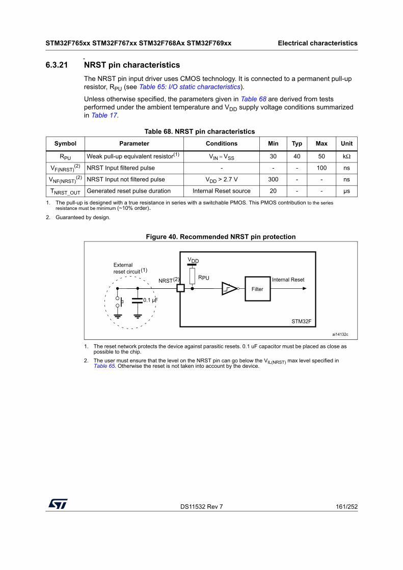
DS11532 Rev 7 161/252
STM32F765xx STM32F767xx STM32F768Ax STM32F769xx Electrical characteristics
218
6.3.21 NRST pin characteristics
The NRST pin input driver uses CMOS technology. It is connected to a permanent pull-up resistor, RPU (see Table 65: I/O static characteristics).
Unless otherwise specified, the parameters given in Table 68 are derived from tests performed under the ambient temperature and VDD supply voltage conditions summarized in Table 17.
Figure 40. Recommended NRST pin protection
1. The reset network protects the device against parasitic resets. 0.1 uF capacitor must be placed as close as possible to the chip.
2. The user must ensure that the level on the NRST pin can go below the VIL(NRST) max level specified in Table 65. Otherwise the reset is not taken into account by the device.
Table 68. NRST pin characteristics
Symbol Parameter Conditions Min Typ Max Unit
RPU Weak pull-up equivalent resistor(1) VIN = VSS 30 40 50 kΩ
VF(NRST)(2) NRST Input filtered pulse - - - 100 ns
VNF(NRST)(2) NRST Input not filtered pulse VDD > 2.7 V 300 - - ns
TNRST_OUT Generated reset pulse duration Internal Reset source 20 - - µs
1. The pull-up is designed with a true resistance in series with a switchable PMOS. This PMOS contribution to the series resistance must be minimum (~10% order).
2. Guaranteed by design.
ai14132c
STM32F
RPUNRST(2)
VDD
Filter
Internal Reset
0.1 μF
Externalreset circuit (1)
Electrical characteristics STM32F765xx STM32F767xx STM32F768Ax STM32F769xx
162/252 DS11532 Rev 7
6.3.22 TIM timer characteristics
The parameters given in Table 69 are guaranteed by design.
Refer to Section 6.3.20: I/O port characteristics for details on the input/output alternate function characteristics (output compare, input capture, external clock, PWM output).
6.3.23 RTC characteristics
6.3.24 12-bit ADC characteristics
Unless otherwise specified, the parameters given in Table 71 are derived from tests performed under the ambient temperature, fPCLK2 frequency and VDDA supply voltage conditions summarized in Table 17.
Table 69. TIMx characteristics(1)(2)
1. TIMx is used as a general term to refer to the TIM1 to TIM12 timers.
2. Guaranteed by design.
Symbol Parameter Conditions(3)
3. The maximum timer frequency on APB1 or APB2 is up to 216 MHz, by setting the TIMPRE bit in the RCC_DCKCFGR register, if APBx prescaler is 1 or 2 or 4, then TIMxCLK = HCLK, otherwise TIMxCLK = 4x PCLKx.
Min Max Unit
tres(TIM) Timer resolution time
AHB/APBx prescaler=1 or 2 or 4, fTIMxCLK =
216 MHz1 - tTIMxCLK
AHB/APBx prescaler>4, fTIMxCLK =
100 MHz1 - tTIMxCLK
fEXTTimer external clock frequency on CH1 to CH4 fTIMxCLK = 216 MHz
0 fTIMxCLK/2 MHz
ResTIM Timer resolution - 16/32 bit
tMAX_COUNTMaximum possible count with 32-bit counter
- -65536 × 65536
tTIMxCLK
Table 70. RTC characteristics
Symbol Parameter Conditions Min Max
- fPCLK1/RTCCLK frequency ratioAny read/write operation from/to an RTC register
4 -
Table 71. ADC characteristics
Symbol Parameter Conditions Min Typ Max Unit
VDDA Power supply VDDA − VREF+ < 1.2 V
1.7(1) - 3.6 V
VREF+ Positive reference voltage 1.7(1) - VDDA V
fADC ADC clock frequencyVDDA = 1.7(1) to 2.4 V 0.6 15 18 MHz
VDDA = 2.4 to 3.6 V 0.6 30 36 MHz
DS11532 Rev 7 163/252
STM32F765xx STM32F767xx STM32F768Ax STM32F769xx Electrical characteristics
218
fTRIG(2) External trigger frequency
fADC = 30 MHz, 12-bit resolution
- - 1764 kHz
- - - 17 1/fADC
VAIN Conversion voltage range(3) -0
(VSSA or VREF- tied to ground)
- VREF+ V
RAIN(2) External input impedance
See Equation 1 for details
- - 50 kΩ
RADC(2)(4) Sampling switch resistance - 1.5 - 6 kΩ
CADC(2) Internal sample and hold
capacitor - - 4 7 pF
tlat(2) Injection trigger conversion
latency
fADC = 30 MHz - - 0.100 µs
- - - 3(5) 1/fADC
tlatr(2) Regular trigger conversion
latency
fADC = 30 MHz - - 0.067 µs
- - - 2(5) 1/fADC
tS(2) Sampling time
fADC = 30 MHz 0.100 - 16 µs
- 3 - 480 1/fADC
tSTAB(2) Power-up time - - 2 3 µs
tCONV(2) Total conversion time (including
sampling time)
fADC = 30 MHz
12-bit resolution0.50 - 16.40 µs
fADC = 30 MHz
10-bit resolution0.43 - 16.34 µs
fADC = 30 MHz
8-bit resolution0.37 - 16.27 µs
fADC = 30 MHz
6-bit resolution0.30 - 16.20 µs
9 to 492 (tS for sampling +n-bit resolution for successive approximation)
1/fADC
fS(2)
Sampling rate
(fADC = 36 MHz, and tS = 3 ADC cycles)
12-bit resolution
Single ADC- - 2.4 Msps
12-bit resolution
Interleave Dual ADC mode
- - 4.5 Msps
12-bit resolution
Interleave Triple ADC mode
- - 7.2 Msps
Table 71. ADC characteristics (continued)
Symbol Parameter Conditions Min Typ Max Unit
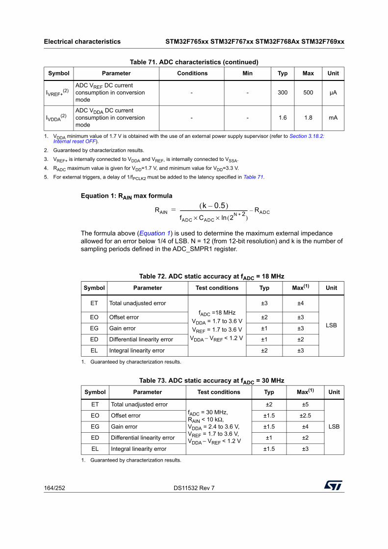
Electrical characteristics STM32F765xx STM32F767xx STM32F768Ax STM32F769xx
164/252 DS11532 Rev 7
Equation 1: RAIN max formula
The formula above (Equation 1) is used to determine the maximum external impedance allowed for an error below 1/4 of LSB. N = 12 (from 12-bit resolution) and k is the number of sampling periods defined in the ADC_SMPR1 register.
IVREF+(2)
ADC VREF DC current consumption in conversion mode
- - 300 500 µA
IVDDA(2)
ADC VDDA DC current consumption in conversion mode
- - 1.6 1.8 mA
1. VDDA minimum value of 1.7 V is obtained with the use of an external power supply supervisor (refer to Section 3.18.2: Internal reset OFF).
2. Guaranteed by characterization results.
3. VREF+ is internally connected to VDDA and VREF- is internally connected to VSSA.
4. RADC maximum value is given for VDD=1.7 V, and minimum value for VDD=3.3 V.
5. For external triggers, a delay of 1/fPCLK2 must be added to the latency specified in Table 71.
Table 71. ADC characteristics (continued)
Symbol Parameter Conditions Min Typ Max Unit
Table 72. ADC static accuracy at fADC = 18 MHz
Symbol Parameter Test conditions Typ Max(1)
1. Guaranteed by characterization results.
Unit
ET Total unadjusted error
fADC =18 MHz
VDDA = 1.7 to 3.6 V
VREF = 1.7 to 3.6 V
VDDA − VREF < 1.2 V
±3 ±4
LSBEO Offset error ±2 ±3
EG Gain error ±1 ±3
ED Differential linearity error ±1 ±2
EL Integral linearity error ±2 ±3
Table 73. ADC static accuracy at fADC = 30 MHz
Symbol Parameter Test conditions Typ Max(1)
1. Guaranteed by characterization results.
Unit
ET Total unadjusted errorfADC = 30 MHz, RAIN < 10 kΩ, VDDA = 2.4 to 3.6 V, VREF = 1.7 to 3.6 V, VDDA − VREF < 1.2 V
±2 ±5
LSB
EO Offset error ±1.5 ±2.5
EG Gain error ±1.5 ±4
ED Differential linearity error ±1 ±2
EL Integral linearity error ±1.5 ±3
RAINk 0.5–( )
fADC CADC 2N 2+( )ln××
-------------------------------------------------------------- RADC–=
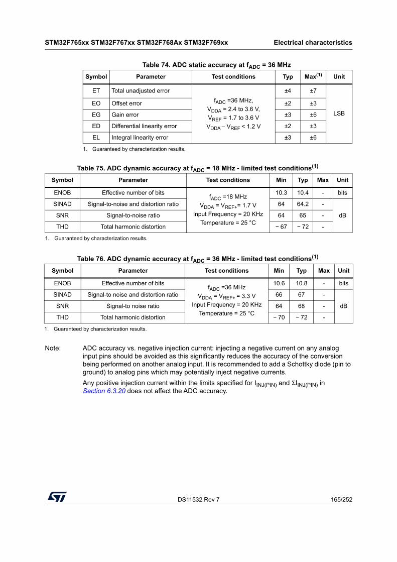
DS11532 Rev 7 165/252
STM32F765xx STM32F767xx STM32F768Ax STM32F769xx Electrical characteristics
218
Note: ADC accuracy vs. negative injection current: injecting a negative current on any analog input pins should be avoided as this significantly reduces the accuracy of the conversion being performed on another analog input. It is recommended to add a Schottky diode (pin to ground) to analog pins which may potentially inject negative currents.
Any positive injection current within the limits specified for IINJ(PIN) and ΣIINJ(PIN) in Section 6.3.20 does not affect the ADC accuracy.
Table 74. ADC static accuracy at fADC = 36 MHz
Symbol Parameter Test conditions Typ Max(1)
1. Guaranteed by characterization results.
Unit
ET Total unadjusted error
fADC =36 MHz,
VDDA = 2.4 to 3.6 V,
VREF = 1.7 to 3.6 V
VDDA − VREF < 1.2 V
±4 ±7
LSB
EO Offset error ±2 ±3
EG Gain error ±3 ±6
ED Differential linearity error ±2 ±3
EL Integral linearity error ±3 ±6
Table 75. ADC dynamic accuracy at fADC = 18 MHz - limited test conditions(1)
Symbol Parameter Test conditions Min Typ Max Unit
ENOB Effective number of bitsfADC =18 MHz
VDDA = VREF+= 1.7 V
Input Frequency = 20 KHz
Temperature = 25 °C
10.3 10.4 - bits
SINAD Signal-to-noise and distortion ratio 64 64.2 -
dBSNR Signal-to-noise ratio 64 65 -
THD Total harmonic distortion − 67 − 72 -
1. Guaranteed by characterization results.
Table 76. ADC dynamic accuracy at fADC = 36 MHz - limited test conditions(1)
Symbol Parameter Test conditions Min Typ Max Unit
ENOB Effective number of bitsfADC =36 MHz
VDDA = VREF+ = 3.3 V
Input Frequency = 20 KHz
Temperature = 25 °C
10.6 10.8 - bits
SINAD Signal-to noise and distortion ratio 66 67 -
dBSNR Signal-to noise ratio 64 68 -
THD Total harmonic distortion − 70 − 72 -
1. Guaranteed by characterization results.
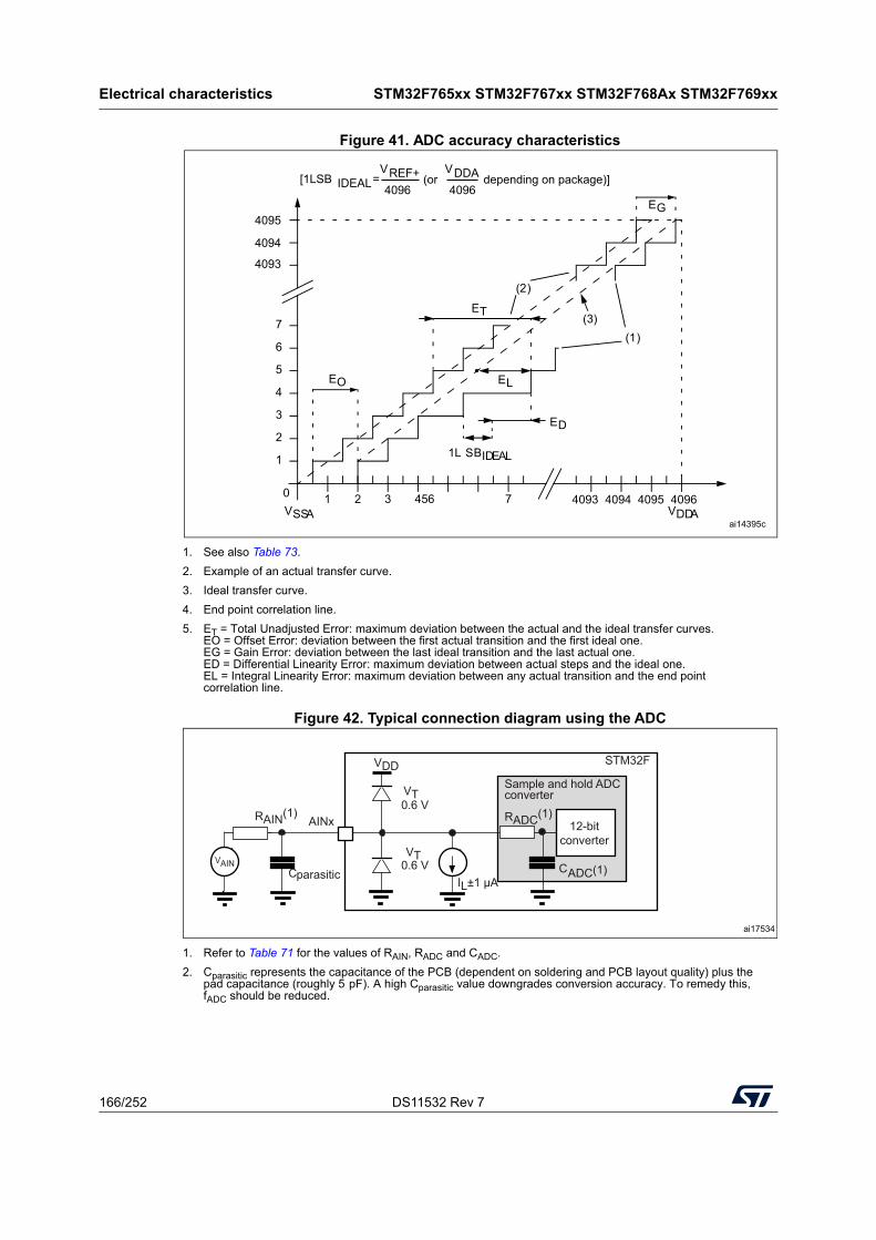
Electrical characteristics STM32F765xx STM32F767xx STM32F768Ax STM32F769xx
166/252 DS11532 Rev 7
Figure 41. ADC accuracy characteristics
1. See also Table 73.
2. Example of an actual transfer curve.
3. Ideal transfer curve.
4. End point correlation line.
5. ET = Total Unadjusted Error: maximum deviation between the actual and the ideal transfer curves. EO = Offset Error: deviation between the first actual transition and the first ideal one. EG = Gain Error: deviation between the last ideal transition and the last actual one. ED = Differential Linearity Error: maximum deviation between actual steps and the ideal one. EL = Integral Linearity Error: maximum deviation between any actual transition and the end point correlation line.
Figure 42. Typical connection diagram using the ADC
1. Refer to Table 71 for the values of RAIN, RADC and CADC.
2. Cparasitic represents the capacitance of the PCB (dependent on soldering and PCB layout quality) plus the pad capacitance (roughly 5 pF). A high Cparasitic value downgrades conversion accuracy. To remedy this, fADC should be reduced.
ai14395c
EO
EG
1L SBIDEAL
4095
4094
4093
5
4
3
2
1
0
7
6
1 2 3 456 7 4093 4094 4095 4096
(1)
(2)
ET
ED
EL
(3)
VDDAVSSA
VREF+4096
(or depending on package)]VDDA4096
[1LSB IDEAL =
ai17534
STM32FVDD
AINx
IL±1 μA0.6 VVT
RAIN(1)
CparasiticVAIN
0.6 VVT
RADC(1)
CADC(1)
12-bitconverter
Sample and hold ADC converter
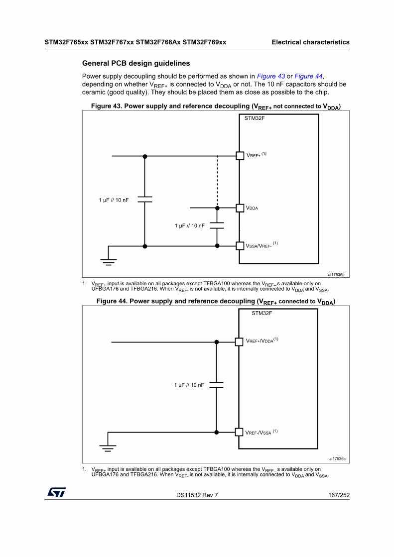
DS11532 Rev 7 167/252
STM32F765xx STM32F767xx STM32F768Ax STM32F769xx Electrical characteristics
218
General PCB design guidelines
Power supply decoupling should be performed as shown in Figure 43 or Figure 44, depending on whether VREF+ is connected to VDDA or not. The 10 nF capacitors should be ceramic (good quality). They should be placed them as close as possible to the chip.
Figure 43. Power supply and reference decoupling (VREF+ not connected to VDDA)
1. VREF+ input is available on all packages except TFBGA100 whereas the VREF– s available only on UFBGA176 and TFBGA216. When VREF- is not available, it is internally connected to VDDA and VSSA.
Figure 44. Power supply and reference decoupling (VREF+ connected to VDDA)
1. VREF+ input is available on all packages except TFBGA100 whereas the VREF– s available only on UFBGA176 and TFBGA216. When VREF- is not available, it is internally connected to VDDA and VSSA.
STM32F
1 μF // 10 nF
1 μF // 10 nF
VREF+ (1)
VDDA
VSSA/VREF- (1)
ai17535b
STM32F
1 μF // 10 nF
ai17536c
VREF+/VDDA
VREF-/VSSA (1)
(1)
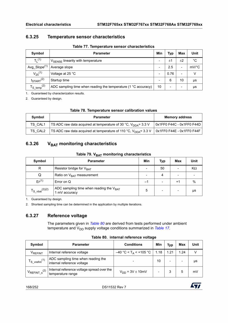
Electrical characteristics STM32F765xx STM32F767xx STM32F768Ax STM32F769xx
168/252 DS11532 Rev 7
6.3.25 Temperature sensor characteristics
6.3.26 VBAT monitoring characteristics
6.3.27 Reference voltage
The parameters given in Table 80 are derived from tests performed under ambient temperature and VDD supply voltage conditions summarized in Table 17.
Table 77. Temperature sensor characteristics
Symbol Parameter Min Typ Max Unit
TL(1) VSENSE linearity with temperature - ±1 ±2 °C
Avg_Slope(1) Average slope - 2.5 - mV/°C
V25(1) Voltage at 25 °C - 0.76 - V
tSTART(2) Startup time - 6 10 µs
TS_temp(2) ADC sampling time when reading the temperature (1 °C accuracy) 10 - - µs
1. Guaranteed by characterization results.
2. Guaranteed by design.
Table 78. Temperature sensor calibration values
Symbol Parameter Memory address
TS_CAL1 TS ADC raw data acquired at temperature of 30 °C, VDDA= 3.3 V 0x1FF0 F44C - 0x1FF0 F44D
TS_CAL2 TS ADC raw data acquired at temperature of 110 °C, VDDA= 3.3 V 0x1FF0 F44E - 0x1FF0 F44F
Table 79. VBAT monitoring characteristics
Symbol Parameter Min Typ Max Unit
R Resistor bridge for VBAT - 50 - KΩ
Q Ratio on VBAT measurement - 4 - -
Er(1) Error on Q –1 - +1 %
TS_vbat(2)(2) ADC sampling time when reading the VBAT
1 mV accuracy 5 - - µs
1. Guaranteed by design.
2. Shortest sampling time can be determined in the application by multiple iterations.
Table 80. internal reference voltage
Symbol Parameter Conditions Min Typ Max Unit
VREFINT Internal reference voltage –40 °C < TA < +105 °C 1.18 1.21 1.24 V
TS_vrefint(1) ADC sampling time when reading the
internal reference voltage- 10 - - µs
VREFINT_s(2) Internal reference voltage spread over the
temperature rangeVDD = 3V ± 10mV - 3 5 mV
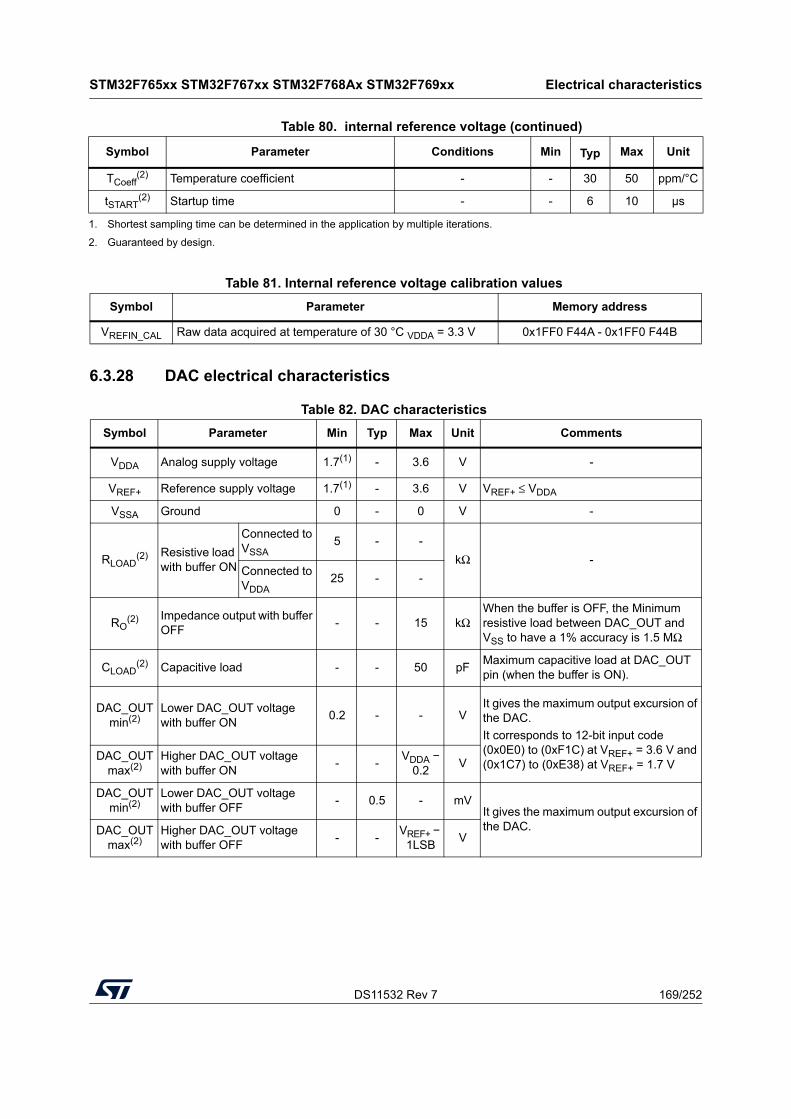
DS11532 Rev 7 169/252
STM32F765xx STM32F767xx STM32F768Ax STM32F769xx Electrical characteristics
218
6.3.28 DAC electrical characteristics
TCoeff(2) Temperature coefficient - - 30 50 ppm/°C
tSTART(2) Startup time - - 6 10 µs
1. Shortest sampling time can be determined in the application by multiple iterations.
2. Guaranteed by design.
Table 80. internal reference voltage (continued)
Symbol Parameter Conditions Min Typ Max Unit
Table 81. Internal reference voltage calibration values
Symbol Parameter Memory address
VREFIN_CAL Raw data acquired at temperature of 30 °C VDDA = 3.3 V 0x1FF0 F44A - 0x1FF0 F44B
Table 82. DAC characteristics
Symbol Parameter Min Typ Max Unit Comments
VDDA Analog supply voltage 1.7(1) - 3.6 V -
VREF+ Reference supply voltage 1.7(1) - 3.6 V VREF+ ≤ VDDA
VSSA Ground 0 - 0 V -
RLOAD(2) Resistive load
with buffer ON
Connected to VSSA
5 - -
kΩ -Connected to VDDA
25 - -
RO(2) Impedance output with buffer
OFF- - 15 kΩ
When the buffer is OFF, the Minimum resistive load between DAC_OUT and VSS to have a 1% accuracy is 1.5 MΩ
CLOAD(2) Capacitive load - - 50 pF
Maximum capacitive load at DAC_OUT pin (when the buffer is ON).
DAC_OUT min(2)
Lower DAC_OUT voltage with buffer ON
0.2 - - VIt gives the maximum output excursion of the DAC.
It corresponds to 12-bit input code (0x0E0) to (0xF1C) at VREF+ = 3.6 V and (0x1C7) to (0xE38) at VREF+ = 1.7 V
DAC_OUT max(2)
Higher DAC_OUT voltage with buffer ON
- -VDDA −
0.2 V
DAC_OUT min(2)
Lower DAC_OUT voltage with buffer OFF
- 0.5 - mVIt gives the maximum output excursion of the DAC.DAC_OUT
max(2)Higher DAC_OUT voltage with buffer OFF
- -VREF+ −
1LSBV
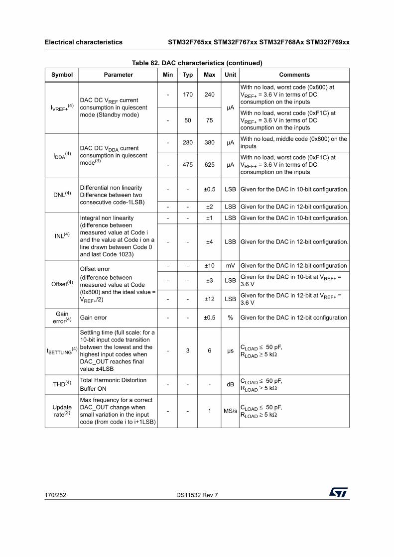
Electrical characteristics STM32F765xx STM32F767xx STM32F768Ax STM32F769xx
170/252 DS11532 Rev 7
IVREF+(4)
DAC DC VREF current consumption in quiescent mode (Standby mode)
- 170 240
µA
With no load, worst code (0x800) at VREF+ = 3.6 V in terms of DC consumption on the inputs
- 50 75With no load, worst code (0xF1C) at VREF+ = 3.6 V in terms of DC consumption on the inputs
IDDA(4)
DAC DC VDDA current consumption in quiescent mode(3)
- 280 380 µAWith no load, middle code (0x800) on the inputs
- 475 625 µAWith no load, worst code (0xF1C) at VREF+ = 3.6 V in terms of DC consumption on the inputs
DNL(4)Differential non linearity Difference between two consecutive code-1LSB)
- - ±0.5 LSB Given for the DAC in 10-bit configuration.
- - ±2 LSB Given for the DAC in 12-bit configuration.
INL(4)
Integral non linearity (difference between measured value at Code i and the value at Code i on a line drawn between Code 0 and last Code 1023)
- - ±1 LSB Given for the DAC in 10-bit configuration.
- - ±4 LSB Given for the DAC in 12-bit configuration.
Offset(4)
Offset error
(difference between measured value at Code (0x800) and the ideal value = VREF+/2)
- - ±10 mV Given for the DAC in 12-bit configuration
- - ±3 LSBGiven for the DAC in 10-bit at VREF+ = 3.6 V
- - ±12 LSBGiven for the DAC in 12-bit at VREF+ = 3.6 V
Gain error(4) Gain error - - ±0.5 % Given for the DAC in 12-bit configuration
tSETTLING(4)
Settling time (full scale: for a 10-bit input code transition between the lowest and the highest input codes when DAC_OUT reaches final value ±4LSB
- 3 6 µsCLOAD ≤ 50 pF, RLOAD ≥ 5 kΩ
THD(4) Total Harmonic Distortion
Buffer ON- - - dB
CLOAD ≤ 50 pF, RLOAD ≥ 5 kΩ
Update rate(2)
Max frequency for a correct DAC_OUT change when small variation in the input code (from code i to i+1LSB)
- - 1 MS/sCLOAD ≤ 50 pF, RLOAD ≥ 5 kΩ
Table 82. DAC characteristics (continued)
Symbol Parameter Min Typ Max Unit Comments

DS11532 Rev 7 171/252
STM32F765xx STM32F767xx STM32F768Ax STM32F769xx Electrical characteristics
218
Figure 45. 12-bit buffered /non-buffered DAC
1. The DAC integrates an output buffer that can be used to reduce the output impedance and to drive external loads directly without the use of an external operational amplifier. The buffer can be bypassed by configuring the BOFFx bit in the DAC_CR register.
6.3.29 Communications interfaces
I2C interface characteristics
The I2C interface meets the timings requirements of the I2C-bus specification and user manual rev. 03 for:
• Standard-mode (Sm): with a bit rate up to 100 kbit/s
• Fast-mode (Fm): with a bit rate up to 400 kbit/s.
• Fast-mode Plus (Fm+): with a bit rate up to 1Mbit/s.
The I2C timings requirements are guaranteed by design when the I2C peripheral is properly configured (refer to RM0410 reference manual) and when the I2CCLK frequency is greater than the minimum shown in the table below:
tWAKEUP(4)
Wakeup time from off state (Setting the ENx bit in the DAC Control register)
- 6.5 10 µsCLOAD ≤ 50 pF, RLOAD ≥ 5 kΩinput code between lowest and highest possible ones.
PSRR+ (2)Power supply rejection ratio (to VDDA) (static DC measurement)
- –67 –40 dB No RLOAD, CLOAD = 50 pF
1. VDDA minimum value of 1.7 V is obtained with the use of an external power supply supervisor (refer to Section 3.18.2: Internal reset OFF).
2. Guaranteed by design.
3. The quiescent mode corresponds to a state where the DAC maintains a stable output level to ensure that no dynamic consumption occurs.
4. Guaranteed by characterization results.
Table 82. DAC characteristics (continued)
Symbol Parameter Min Typ Max Unit Comments
R L
C L
Buffered/Non-buffered DAC
DAC_OUTx
Buffer(1)
12-bit digital to analog converter
ai17157V3
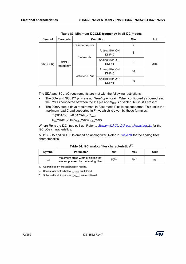
Electrical characteristics STM32F765xx STM32F767xx STM32F768Ax STM32F769xx
172/252 DS11532 Rev 7
The SDA and SCL I/O requirements are met with the following restrictions:
• The SDA and SCL I/O pins are not “true” open-drain. When configured as open-drain, the PMOS connected between the I/O pin and VDD is disabled, but is still present.
• The 20mA output drive requirement in Fast-mode Plus is not supported. This limits the maximum load Cload supported in Fm+, which is given by these formulas:
Tr(SDA/SCL)=0.8473xRpxCload
Rp(min)= (VDD-VOL(max))/IOL(max)
Where Rp is the I2C lines pull-up. Refer to Section 6.3.20: I/O port characteristics for the I2C I/Os characteristics.
All I2C SDA and SCL I/Os embed an analog filter. Refer to Table 84 for the analog filter characteristics:
Table 83. Minimum I2CCLK frequency in all I2C modes
Symbol Parameter Condition Min Unit
f(I2CCLK)I2CCLK
frequency
Standard-mode - 2
MHz
Fast-mode
Analog filter ON
DNF=08
Analog filter OFF
DNF=19
Fast-mode Plus
Analog filter ON
DNF=016
Analog filter OFF
DNF=116
Table 84. I2C analog filter characteristics(1)
1. Guaranteed by characterization results.
Symbol Parameter Min Max Unit
tAFMaximum pulse width of spikes that are suppressed by the analog filter
50(2)
2. Spikes with widths below tAF(min) are filtered.
70(3)
3. Spikes with widths above tAF(max) are not filtered.
ns
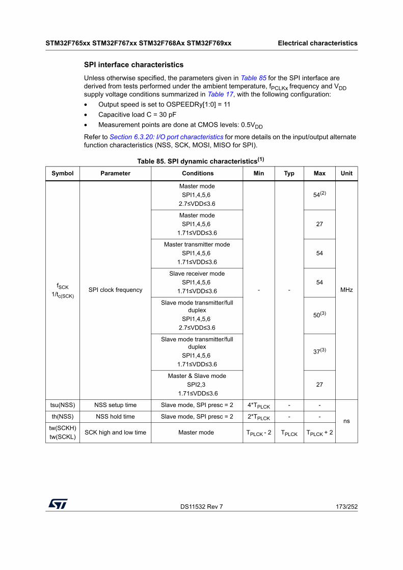
DS11532 Rev 7 173/252
STM32F765xx STM32F767xx STM32F768Ax STM32F769xx Electrical characteristics
218
SPI interface characteristics
Unless otherwise specified, the parameters given in Table 85 for the SPI interface are derived from tests performed under the ambient temperature, fPCLKx frequency and VDD supply voltage conditions summarized in Table 17, with the following configuration:
• Output speed is set to OSPEEDRy[1:0] = 11
• Capacitive load C = 30 pF
• Measurement points are done at CMOS levels: 0.5VDD
Refer to Section 6.3.20: I/O port characteristics for more details on the input/output alternate function characteristics (NSS, SCK, MOSI, MISO for SPI).
Table 85. SPI dynamic characteristics(1)
Symbol Parameter Conditions Min Typ Max Unit
fSCK
1/tc(SCK)SPI clock frequency
Master mode
SPI1,4,5,6
2.7≤VDD≤3.6
- -
54(2)
MHz
Master mode
SPI1,4,5,6
1.71≤VDD≤3.6
27
Master transmitter mode
SPI1,4,5,6
1.71≤VDD≤3.6
54
Slave receiver mode
SPI1,4,5,6
1.71≤VDD≤3.6
54
Slave mode transmitter/full duplex
SPI1,4,5,6
2.7≤VDD≤3.6
50(3)
Slave mode transmitter/full duplex
SPI1,4,5,6
1.71≤VDD≤3.6
37(3)
Master & Slave mode
SPI2,3
1.71≤VDD≤3.6
27
tsu(NSS) NSS setup time Slave mode, SPI presc = 2 4*TPLCK - -
nsth(NSS) NSS hold time Slave mode, SPI presc = 2 2*TPLCK - -
tw(SCKH)
tw(SCKL)SCK high and low time Master mode TPLCK - 2 TPLCK TPLCK + 2
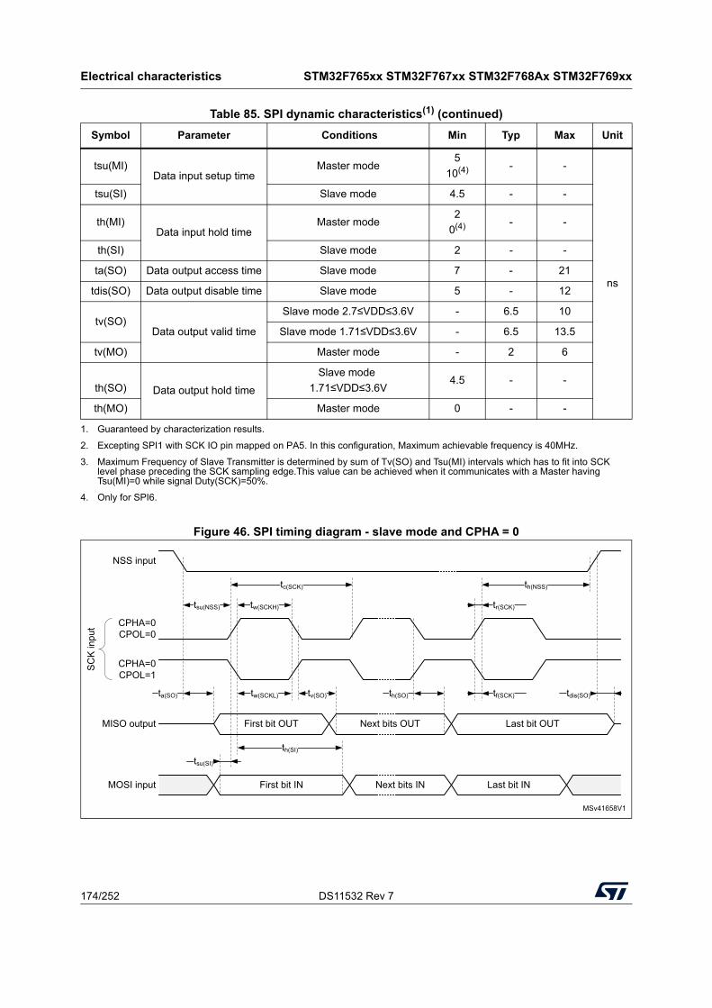
Electrical characteristics STM32F765xx STM32F767xx STM32F768Ax STM32F769xx
174/252 DS11532 Rev 7
Figure 46. SPI timing diagram - slave mode and CPHA = 0
tsu(MI)Data input setup time
Master mode5
10(4) - -
ns
tsu(SI) Slave mode 4.5 - -
th(MI)Data input hold time
Master mode2
0(4) - -
th(SI) Slave mode 2 - -
ta(SO) Data output access time Slave mode 7 - 21
tdis(SO) Data output disable time Slave mode 5 - 12
tv(SO)Data output valid time
Slave mode 2.7≤VDD≤3.6V - 6.5 10
Slave mode 1.71≤VDD≤3.6V - 6.5 13.5
tv(MO) Master mode - 2 6
th(SO) Data output hold time
Slave mode
1.71≤VDD≤3.6V4.5 - -
th(MO) Master mode 0 - -
1. Guaranteed by characterization results.
2. Excepting SPI1 with SCK IO pin mapped on PA5. In this configuration, Maximum achievable frequency is 40MHz.
3. Maximum Frequency of Slave Transmitter is determined by sum of Tv(SO) and Tsu(MI) intervals which has to fit into SCK level phase preceding the SCK sampling edge.This value can be achieved when it communicates with a Master having Tsu(MI)=0 while signal Duty(SCK)=50%.
4. Only for SPI6.
Table 85. SPI dynamic characteristics(1) (continued)
Symbol Parameter Conditions Min Typ Max Unit
MSv41658V1
NSS input
CPHA=0CPOL=0
SC
K in
put
CPHA=0CPOL=1
MISO output
MOSI input
tsu(SI)
th(SI)
tw(SCKL)
tw(SCKH)
tc(SCK)
tr(SCK)
th(NSS)
tdis(SO)
tsu(NSS)
ta(SO) tv(SO)
Next bits IN
Last bit OUT
First bit IN
First bit OUT Next bits OUT
th(SO) tf(SCK)
Last bit IN
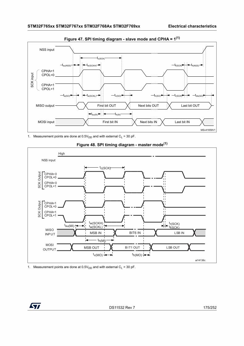
DS11532 Rev 7 175/252
STM32F765xx STM32F767xx STM32F768Ax STM32F769xx Electrical characteristics
218
Figure 47. SPI timing diagram - slave mode and CPHA = 1(1)
1. Measurement points are done at 0.5VDD and with external CL = 30 pF.
Figure 48. SPI timing diagram - master mode(1)
1. Measurement points are done at 0.5VDD and with external CL = 30 pF.
MSv41659V1
NSS input
CPHA=1CPOL=0
SC
K in
put
CPHA=1CPOL=1
MISO output
MOSI input
tsu(SI) th(SI)
tw(SCKL)
tw(SCKH)tsu(NSS)
tc(SCK)
ta(SO) tv(SO)
First bit OUT Next bits OUT
Next bits IN
Last bit OUT
th(SO) tr(SCK)
tf(SCK) th(NSS)
tdis(SO)
First bit IN Last bit IN
ai14136c
SCK
Out
put
CPHA=0
MOSIOUTPUT
MISOINPUT
CPHA=0
LSB OUT
LSB IN
CPOL=0
CPOL=1
BIT1 OUT
NSS input
tc(SCK)
tw(SCKH)tw(SCKL)
tr(SCK)tf(SCK)
th(MI)
High
SCK
Out
put
CPHA=1
CPHA=1
CPOL=0
CPOL=1
tsu(MI)
tv(MO) th(MO)
MSB IN BIT6 IN
MSB OUT
Electrical characteristics STM32F765xx STM32F767xx STM32F768Ax STM32F769xx
176/252 DS11532 Rev 7
I2S interface characteristics
Unless otherwise specified, the parameters given in Table 86 for the I2S interface are derived from tests performed under the ambient temperature, fPCLKx frequency and VDD supply voltage conditions summarized in Table 17, with the following configuration:
• Output speed is set to OSPEEDRy[1:0] = 10
• Capacitive load C = 30 pF
• Measurement points are done at CMOS levels: 0.5VDD
Refer to Section 6.3.20: I/O port characteristics for more details on the input/output alternate function characteristics (CK, SD, WS).
Note: Refer to RM0410 reference manual I2S section for more details about the sampling frequency (FS). fMCK, fCK, and DCK values reflect only the digital peripheral behavior. The values of these parameters might be slightly impacted by the source clock precision. DCK depends mainly on the value of ODD bit. The digital contribution leads to a minimum value of (I2SDIV/(2*I2SDIV+ODD) and a maximum value of (I2SDIV+ODD)/(2*I2SDIV+ODD). FS maximum value is supported for each mode/condition.
Table 86. I2S dynamic characteristics(1)
Symbol Parameter Conditions Min Max Unit
fMCK I2S Main clock output - 256x8K 256xFs(2) MHz
fCK I2S clock frequency Master data - 64xFs
MHzSlave data - 64xFs
DCK I2S clock frequency duty cycle Slave receiver 30 70 %
tv(WS) WS valid time Master mode - 3
ns
th(WS) WS hold time Master mode 0 -
tsu(WS) WS setup time Slave mode 5 -
th(WS) WS hold time Slave mode 2 -
tsu(SD_MR)Data input setup time
Master receiver 2.5 -
tsu(SD_SR) Slave receiver 2.5 -
th(SD_MR)Data input hold time
Master receiver 3.5 -
th(SD_SR) Slave receiver 2 -
tv(SD_ST)Data output valid time
Slave transmitter (after enable edge) - 12
tv(SD_MT) Master transmitter (after enable edge) - 3
th(SD_ST)Data output hold time
Slave transmitter (after enable edge) 5 -
th(SD_MT) Master transmitter (after enable edge) 0 -
1. Guaranteed by characterization results.
2. The maximum value of 256xFs is 49.152 MHz (APB1 maximum frequency).
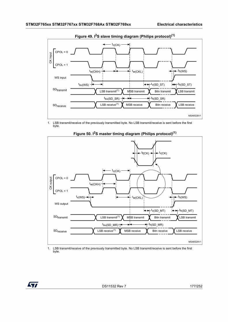
DS11532 Rev 7 177/252
STM32F765xx STM32F767xx STM32F768Ax STM32F769xx Electrical characteristics
218
Figure 49. I2S slave timing diagram (Philips protocol)(1)
1. LSB transmit/receive of the previously transmitted byte. No LSB transmit/receive is sent before the first byte.
Figure 50. I2S master timing diagram (Philips protocol)(1)
1. LSB transmit/receive of the previously transmitted byte. No LSB transmit/receive is sent before the first byte.
CK
Inpu
t CPOL = 0
CPOL = 1
tc(CK)
WS input
SDtransmit
SDreceive
tw(CKH) tw(CKL)
tsu(WS) tv(SD_ST) th(SD_ST)
th(WS)
tsu(SD_SR) th(SD_SR)
MSB receive Bitn receive LSB receive
MSB transmit Bitn transmit LSB transmit
MS46528V1
LSB receive(1)
LSB transmit(1)
CK
out
put CPOL = 0
CPOL = 1
tc(CK)
WS output
SDreceive
SDtransmit
tw(CKH)
tw(CKL)
tsu(SD_MR)
tv(SD_MT) th(SD_MT)
th(WS)
th(SD_MR)
MSB receive Bitn receive LSB receive
MSB transmit Bitn transmit LSB transmit
MS46529V1
tf(CK) tr(CK)
tv(WS)
LSB receive(1)
LSB transmit(1)
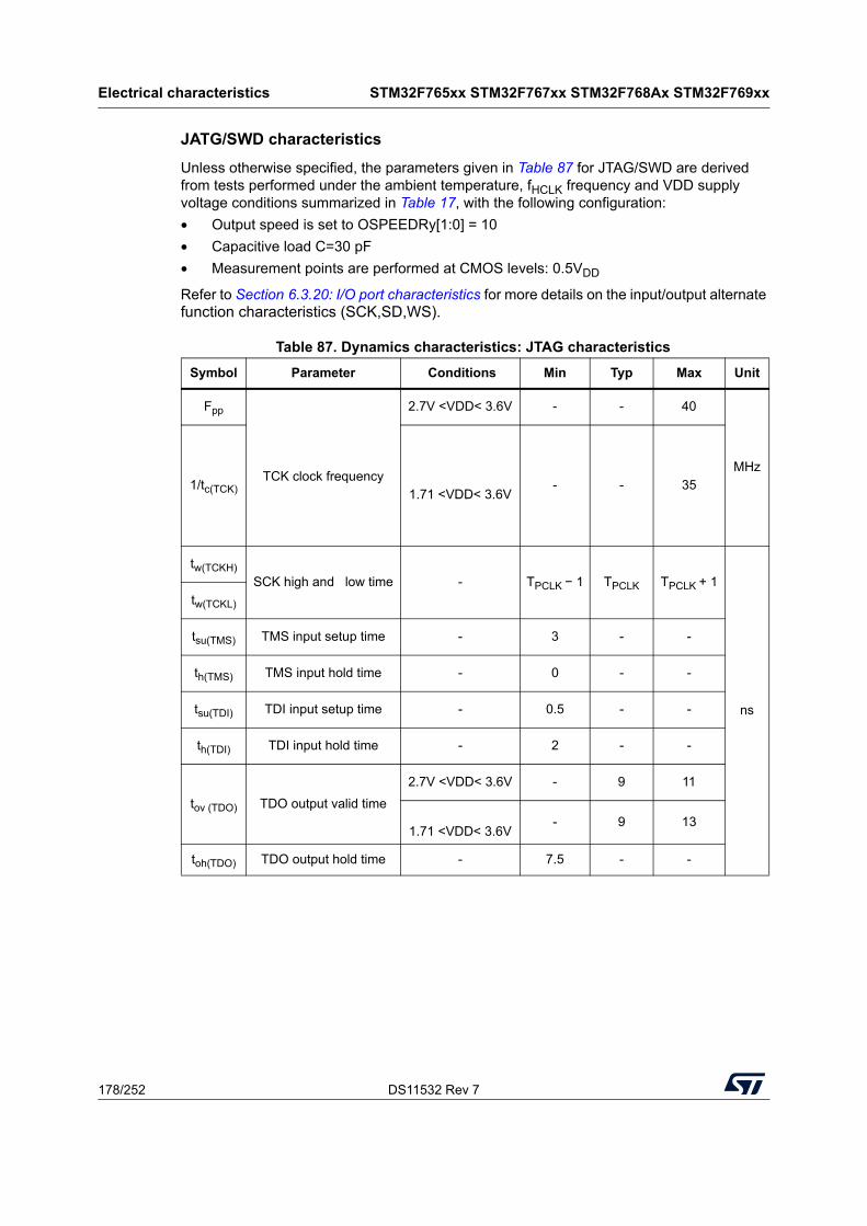
Electrical characteristics STM32F765xx STM32F767xx STM32F768Ax STM32F769xx
178/252 DS11532 Rev 7
JATG/SWD characteristics
Unless otherwise specified, the parameters given in Table 87 for JTAG/SWD are derived from tests performed under the ambient temperature, fHCLK frequency and VDD supply voltage conditions summarized in Table 17, with the following configuration:
• Output speed is set to OSPEEDRy[1:0] = 10
• Capacitive load C=30 pF
• Measurement points are performed at CMOS levels: 0.5VDD
Refer to Section 6.3.20: I/O port characteristics for more details on the input/output alternate function characteristics (SCK,SD,WS).
Table 87. Dynamics characteristics: JTAG characteristics
Symbol Parameter Conditions Min Typ Max Unit
Fpp
TCK clock frequency
2.7V <VDD< 3.6V - - 40
MHz1/tc(TCK) 1.71 <VDD< 3.6V
- - 35
tw(TCKH)
SCK high and low time - TPCLK − 1 TPCLK TPCLK + 1
ns
tw(TCKL)
tsu(TMS) TMS input setup time - 3 - -
th(TMS) TMS input hold time - 0 - -
tsu(TDI) TDI input setup time - 0.5 - -
th(TDI) TDI input hold time - 2 - -
tov (TDO) TDO output valid time
2.7V <VDD< 3.6V - 9 11
1.71 <VDD< 3.6V- 9 13
toh(TDO) TDO output hold time - 7.5 - -
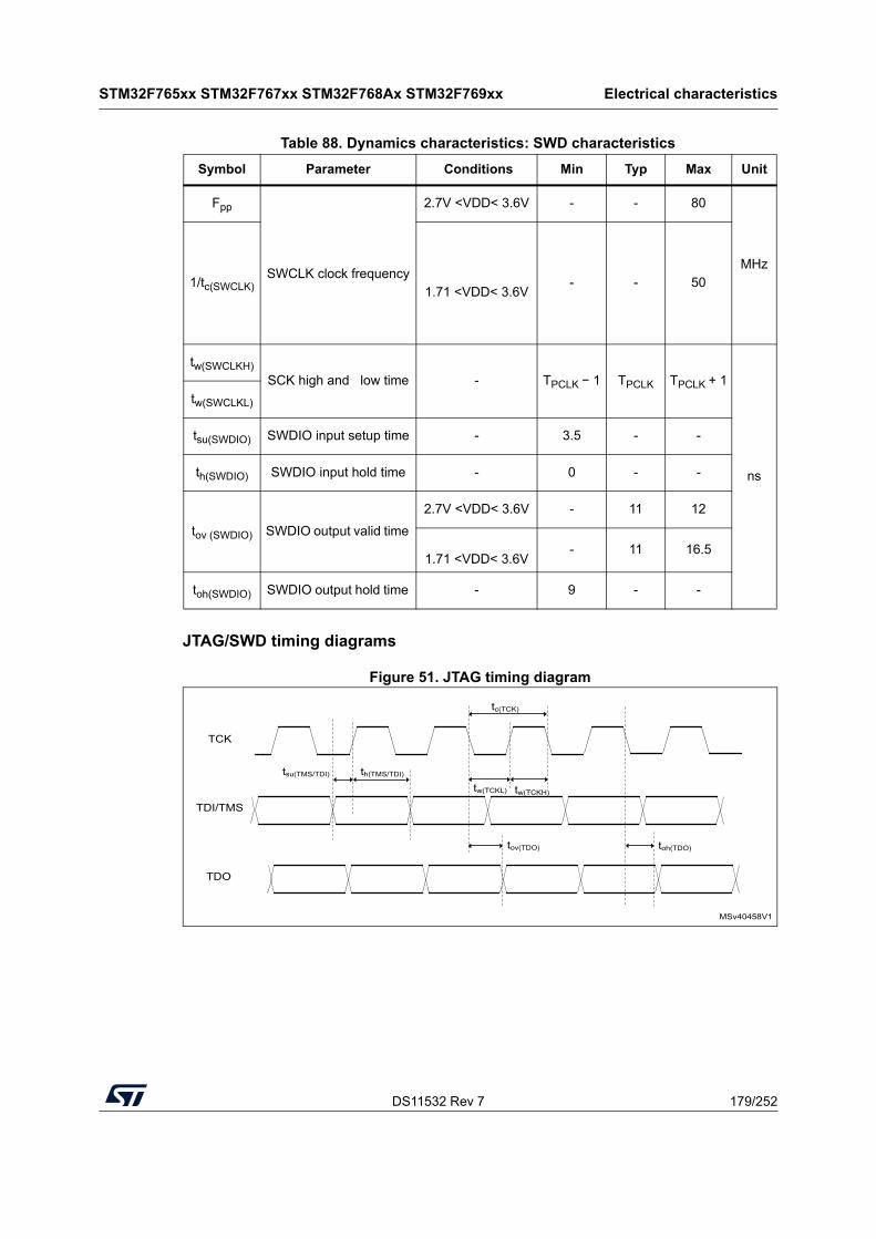
DS11532 Rev 7 179/252
STM32F765xx STM32F767xx STM32F768Ax STM32F769xx Electrical characteristics
218
JTAG/SWD timing diagrams
Figure 51. JTAG timing diagram
Table 88. Dynamics characteristics: SWD characteristics
Symbol Parameter Conditions Min Typ Max Unit
Fpp
SWCLK clock frequency
2.7V <VDD< 3.6V - - 80
MHz1/tc(SWCLK) 1.71 <VDD< 3.6V
- - 50
tw(SWCLKH)
SCK high and low time - TPCLK − 1 TPCLK TPCLK + 1
ns
tw(SWCLKL)
tsu(SWDIO) SWDIO input setup time - 3.5 - -
th(SWDIO) SWDIO input hold time - 0 - -
tov (SWDIO) SWDIO output valid time
2.7V <VDD< 3.6V - 11 12
1.71 <VDD< 3.6V- 11 16.5
toh(SWDIO) SWDIO output hold time - 9 - -
MSv40458V1
TDI/TMS
TCK
TDO
tc(TCK)
tw(TCKL) tw(TCKH)
th(TMS/TDI)tsu(TMS/TDI)
tov(TDO) toh(TDO)
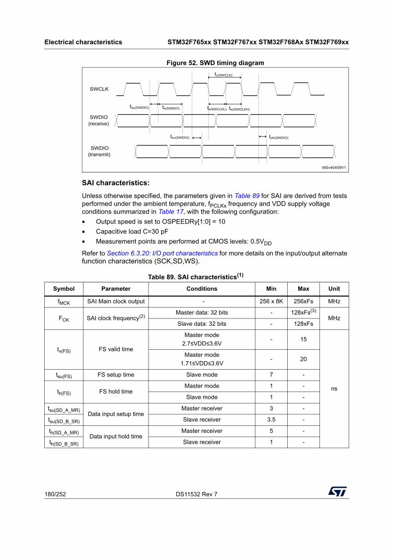
Electrical characteristics STM32F765xx STM32F767xx STM32F768Ax STM32F769xx
180/252 DS11532 Rev 7
Figure 52. SWD timing diagram
SAI characteristics:
Unless otherwise specified, the parameters given in Table 89 for SAI are derived from tests performed under the ambient temperature, fPCLKx frequency and VDD supply voltage conditions summarized in Table 17, with the following configuration:
• Output speed is set to OSPEEDRy[1:0] = 10
• Capacitive load C=30 pF
• Measurement points are performed at CMOS levels: 0.5VDD
Refer to Section 6.3.20: I/O port characteristics for more details on the input/output alternate function characteristics (SCK,SD,WS).
MSv40459V1
SWDIO
SWCLK
SWDIO
tc(SWCLK)
twSWCLKL) tw(SWCLKH)th(SWDIO)tsu(SWDIO)
tov(SWDIO) toh(SWDIO)
(receive)
(transmit)
Table 89. SAI characteristics(1)
Symbol Parameter Conditions Min Max Unit
fMCK SAI Main clock output - 256 x 8K 256xFs MHz
FCK SAI clock frequency(2) Master data: 32 bits - 128xFs(3)
MHzSlave data: 32 bits - 128xFs
tv(FS) FS valid time
Master mode
2.7≤VDD≤3.6V- 15
ns
Master mode
1.71≤VDD≤3.6V- 20
tsu(FS) FS setup time Slave mode 7 -
th(FS) FS hold time Master mode 1 -
Slave mode 1 -
tsu(SD_A_MR)Data input setup time
Master receiver 3 -
tsu(SD_B_SR) Slave receiver 3.5 -
th(SD_A_MR)Data input hold time
Master receiver 5 -
th(SD_B_SR) Slave receiver 1 -
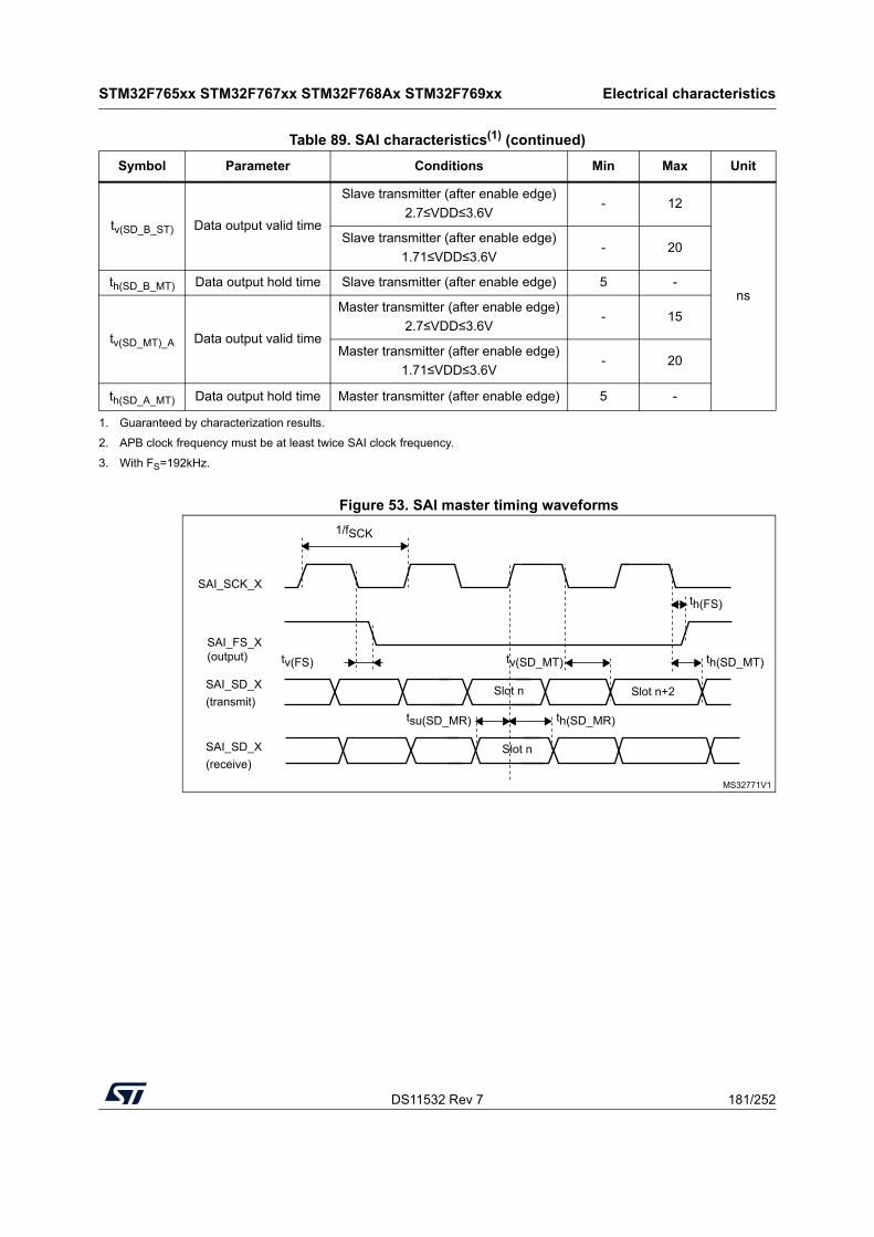
DS11532 Rev 7 181/252
STM32F765xx STM32F767xx STM32F768Ax STM32F769xx Electrical characteristics
218
Figure 53. SAI master timing waveforms
tv(SD_B_ST) Data output valid time
Slave transmitter (after enable edge)
2.7≤VDD≤3.6V- 12
ns
Slave transmitter (after enable edge)
1.71≤VDD≤3.6V- 20
th(SD_B_MT) Data output hold time Slave transmitter (after enable edge) 5 -
tv(SD_MT)_A Data output valid time
Master transmitter (after enable edge)
2.7≤VDD≤3.6V- 15
Master transmitter (after enable edge)
1.71≤VDD≤3.6V- 20
th(SD_A_MT) Data output hold time Master transmitter (after enable edge) 5 -
1. Guaranteed by characterization results.
2. APB clock frequency must be at least twice SAI clock frequency.
3. With FS=192kHz.
Table 89. SAI characteristics(1) (continued)
Symbol Parameter Conditions Min Max Unit
MS32771V1
SAI_SCK_X
SAI_FS_X(output)
1/fSCK
SAI_SD_X(transmit)
tv(FS)
Slot n
SAI_SD_X(receive)
th(FS)
Slot n+2
tv(SD_MT) th(SD_MT)
Slot n
tsu(SD_MR) th(SD_MR)
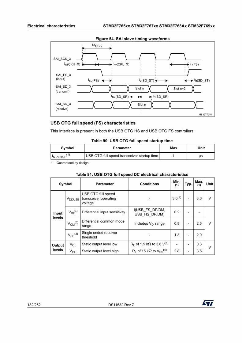
Electrical characteristics STM32F765xx STM32F767xx STM32F768Ax STM32F769xx
182/252 DS11532 Rev 7
Figure 54. SAI slave timing waveforms
USB OTG full speed (FS) characteristics
This interface is present in both the USB OTG HS and USB OTG FS controllers.
Table 90. USB OTG full speed startup time
Symbol Parameter Max Unit
tSTARTUP(1)
1. Guaranteed by design.
USB OTG full speed transceiver startup time 1 µs
Table 91. USB OTG full speed DC electrical characteristics
Symbol Parameter ConditionsMin.
(1) Typ.Max.
(1) Unit
Input levels
VDDUSB
USB OTG full speed transceiver operating voltage
- 3.0(2) - 3.6 V
VDI(3) Differential input sensitivity
I(USB_FS_DP/DM, USB_HS_DP/DM)
0.2 - -
VVCM(3) Differential common mode
rangeIncludes VDI range 0.8 - 2.5
VSE(3) Single ended receiver
threshold- 1.3 - 2.0
Output levels
VOL Static output level low RL of 1.5 kΩ to 3.6 V(4) - - 0.3V
VOH Static output level high RL of 15 kΩ to VSS(4) 2.8 - 3.6
MS32772V1
SAI_SCK_X
SAI_FS_X(input)
SAI_SD_X(transmit)
tsu(FS)
Slot n
SAI_SD_X(receive)
tw(CKH_X) th(FS)
Slot n+2
tv(SD_ST) th(SD_ST)
Slot n
tsu(SD_SR)
tw(CKL_X)
th(SD_SR)
1/fSCK
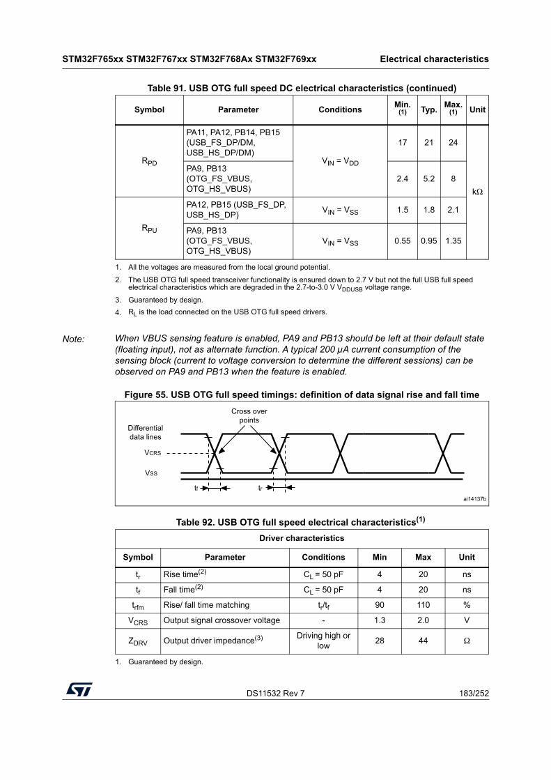
DS11532 Rev 7 183/252
STM32F765xx STM32F767xx STM32F768Ax STM32F769xx Electrical characteristics
218
Note: When VBUS sensing feature is enabled, PA9 and PB13 should be left at their default state (floating input), not as alternate function. A typical 200 µA current consumption of the sensing block (current to voltage conversion to determine the different sessions) can be observed on PA9 and PB13 when the feature is enabled.
Figure 55. USB OTG full speed timings: definition of data signal rise and fall time
RPD
PA11, PA12, PB14, PB15 (USB_FS_DP/DM, USB_HS_DP/DM)
VIN = VDD
17 21 24
kΩ
PA9, PB13 (OTG_FS_VBUS, OTG_HS_VBUS)
2.4 5.2 8
RPU
PA12, PB15 (USB_FS_DP, USB_HS_DP)
VIN = VSS 1.5 1.8 2.1
PA9, PB13 (OTG_FS_VBUS, OTG_HS_VBUS)
VIN = VSS 0.55 0.95 1.35
1. All the voltages are measured from the local ground potential.
2. The USB OTG full speed transceiver functionality is ensured down to 2.7 V but not the full USB full speed electrical characteristics which are degraded in the 2.7-to-3.0 V VDDUSB voltage range.
3. Guaranteed by design.
4. RL is the load connected on the USB OTG full speed drivers.
Table 91. USB OTG full speed DC electrical characteristics (continued)
Symbol Parameter ConditionsMin.
(1) Typ.Max.
(1) Unit
Table 92. USB OTG full speed electrical characteristics(1)
1. Guaranteed by design.
Driver characteristics
Symbol Parameter Conditions Min Max Unit
tr Rise time(2) CL = 50 pF 4 20 ns
tf Fall time(2) CL = 50 pF 4 20 ns
trfm Rise/ fall time matching tr/tf 90 110 %
VCRS Output signal crossover voltage - 1.3 2.0 V
ZDRV Output driver impedance(3) Driving high or low
28 44 Ω
ai14137b
Cross overpoints
Differentialdata lines
VCRS
VSS
tf tr
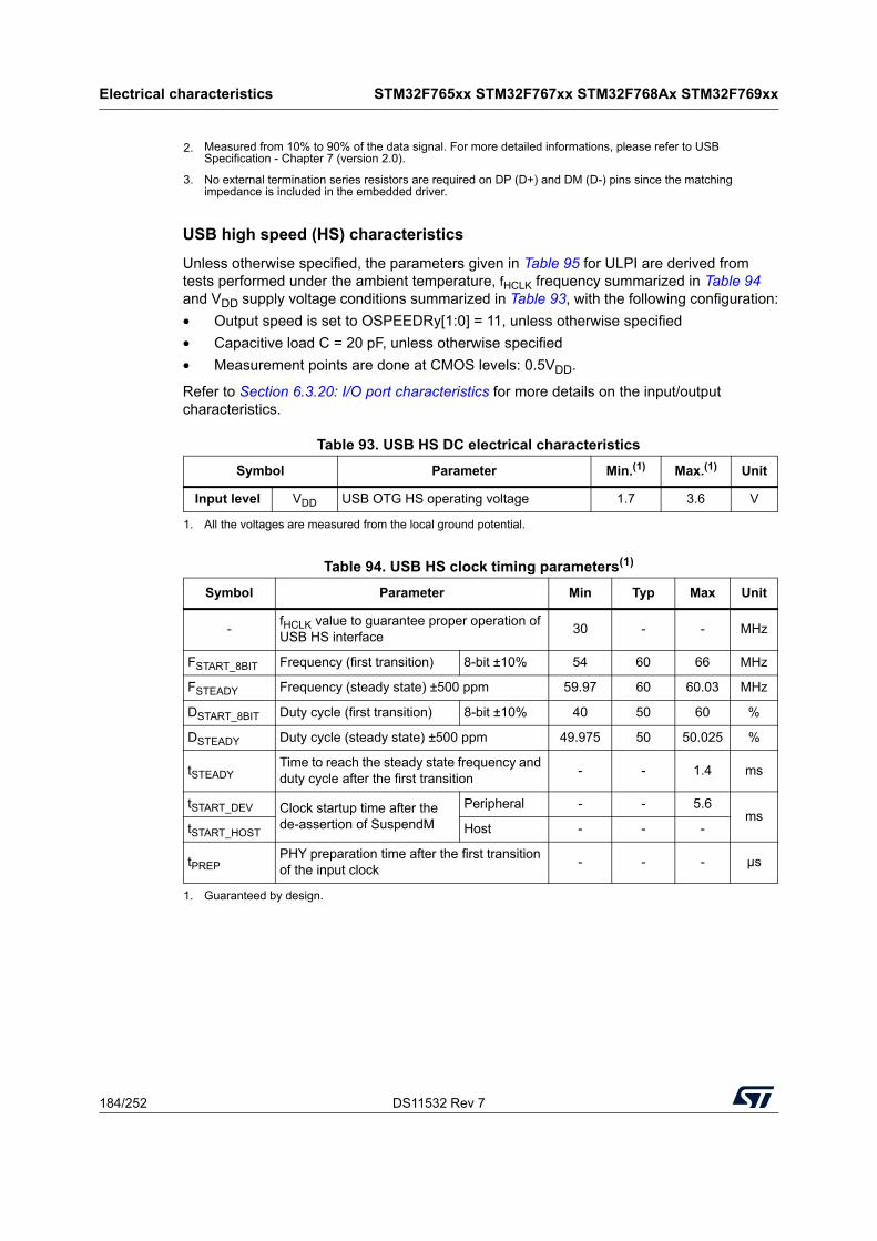
Electrical characteristics STM32F765xx STM32F767xx STM32F768Ax STM32F769xx
184/252 DS11532 Rev 7
USB high speed (HS) characteristics
Unless otherwise specified, the parameters given in Table 95 for ULPI are derived from tests performed under the ambient temperature, fHCLK frequency summarized in Table 94 and VDD supply voltage conditions summarized in Table 93, with the following configuration:
• Output speed is set to OSPEEDRy[1:0] = 11, unless otherwise specified
• Capacitive load C = 20 pF, unless otherwise specified
• Measurement points are done at CMOS levels: 0.5VDD.
Refer to Section 6.3.20: I/O port characteristics for more details on the input/output characteristics.
2. Measured from 10% to 90% of the data signal. For more detailed informations, please refer to USB Specification - Chapter 7 (version 2.0).
3. No external termination series resistors are required on DP (D+) and DM (D-) pins since the matching impedance is included in the embedded driver.
Table 93. USB HS DC electrical characteristics
Symbol Parameter Min.(1)
1. All the voltages are measured from the local ground potential.
Max.(1) Unit
Input level VDD USB OTG HS operating voltage 1.7 3.6 V
Table 94. USB HS clock timing parameters(1)
1. Guaranteed by design.
Symbol Parameter Min Typ Max Unit
-fHCLK value to guarantee proper operation of USB HS interface
30 - - MHz
FSTART_8BIT Frequency (first transition) 8-bit ±10% 54 60 66 MHz
FSTEADY Frequency (steady state) ±500 ppm 59.97 60 60.03 MHz
DSTART_8BIT Duty cycle (first transition) 8-bit ±10% 40 50 60 %
DSTEADY Duty cycle (steady state) ±500 ppm 49.975 50 50.025 %
tSTEADYTime to reach the steady state frequency and duty cycle after the first transition
- - 1.4 ms
tSTART_DEV Clock startup time after the de-assertion of SuspendM
Peripheral - - 5.6ms
tSTART_HOST Host - - -
tPREPPHY preparation time after the first transition of the input clock
- - - µs
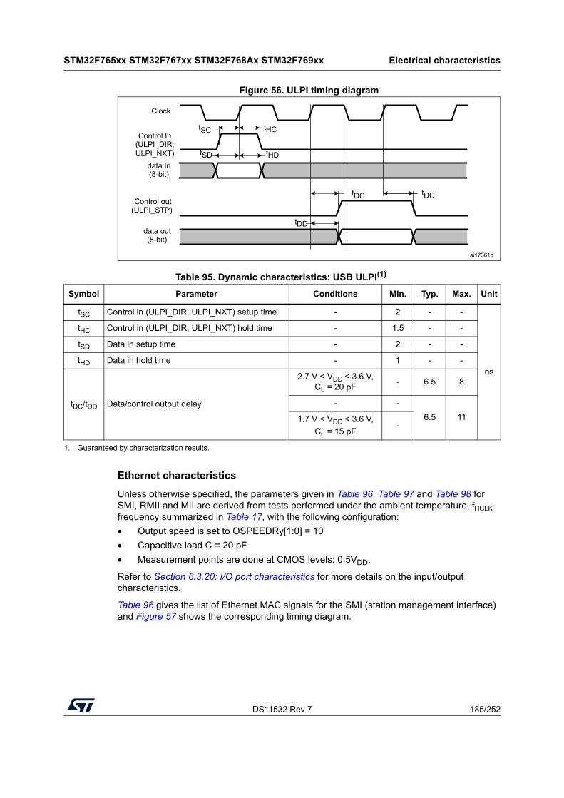
DS11532 Rev 7 185/252
STM32F765xx STM32F767xx STM32F768Ax STM32F769xx Electrical characteristics
218
Figure 56. ULPI timing diagram
Ethernet characteristics
Unless otherwise specified, the parameters given in Table 96, Table 97 and Table 98 for SMI, RMII and MII are derived from tests performed under the ambient temperature, fHCLK frequency summarized in Table 17, with the following configuration:
• Output speed is set to OSPEEDRy[1:0] = 10
• Capacitive load C = 20 pF
• Measurement points are done at CMOS levels: 0.5VDD.
Refer to Section 6.3.20: I/O port characteristics for more details on the input/output characteristics.
Table 96 gives the list of Ethernet MAC signals for the SMI (station management interface) and Figure 57 shows the corresponding timing diagram.
Clock
Control In(ULPI_DIR,ULPI_NXT)
data In(8-bit)
Control out(ULPI_STP)
data out(8-bit)
tDD
tDC
tHDtSD
tHCtSC
ai17361c
tDC
Table 95. Dynamic characteristics: USB ULPI(1)
Symbol Parameter Conditions Min. Typ. Max. Unit
tSC Control in (ULPI_DIR, ULPI_NXT) setup time - 2 - -
ns
tHC Control in (ULPI_DIR, ULPI_NXT) hold time - 1.5 - -
tSD Data in setup time - 2 - -
tHD Data in hold time - 1 - -
tDC/tDD Data/control output delay
2.7 V < VDD < 3.6 V, CL = 20 pF
- 6.5 8
- -
6.5 111.7 V < VDD < 3.6 V,
CL = 15 pF-
1. Guaranteed by characterization results.
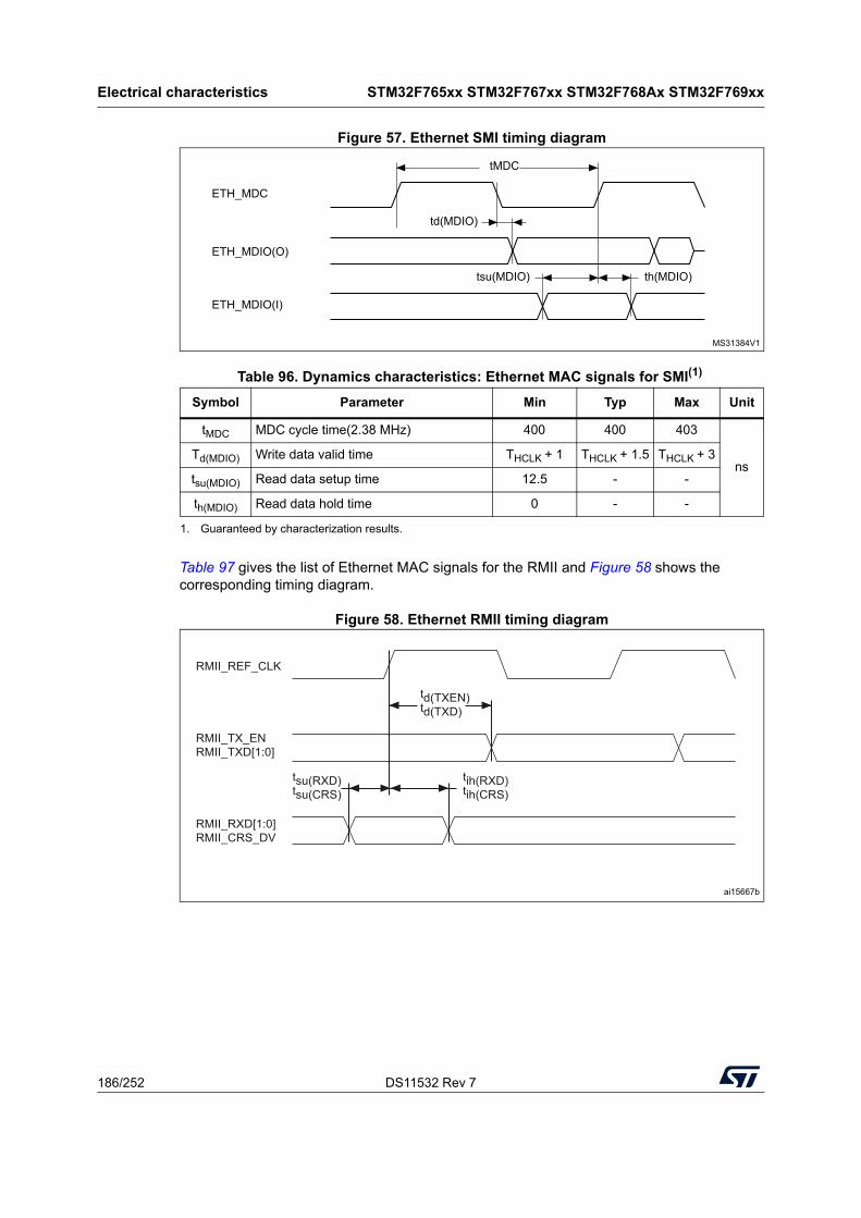
Electrical characteristics STM32F765xx STM32F767xx STM32F768Ax STM32F769xx
186/252 DS11532 Rev 7
Figure 57. Ethernet SMI timing diagram
Table 97 gives the list of Ethernet MAC signals for the RMII and Figure 58 shows the corresponding timing diagram.
Figure 58. Ethernet RMII timing diagram
Table 96. Dynamics characteristics: Ethernet MAC signals for SMI(1)
1. Guaranteed by characterization results.
Symbol Parameter Min Typ Max Unit
tMDC MDC cycle time(2.38 MHz) 400 400 403
nsTd(MDIO) Write data valid time THCLK + 1 THCLK + 1.5 THCLK + 3
tsu(MDIO) Read data setup time 12.5 - -
th(MDIO) Read data hold time 0 - -
MS31384V1
ETH_MDC
ETH_MDIO(O)
ETH_MDIO(I)
tMDC
td(MDIO)
tsu(MDIO) th(MDIO)
ai15667b
RMII_REF_CLK
RMII_TX_ENRMII_TXD[1:0]
RMII_RXD[1:0]RMII_CRS_DV
td(TXEN)td(TXD)
tsu(RXD)tsu(CRS)
tih(RXD)tih(CRS)
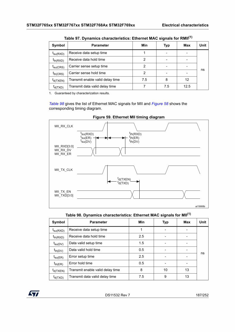
DS11532 Rev 7 187/252
STM32F765xx STM32F767xx STM32F768Ax STM32F769xx Electrical characteristics
218
Table 98 gives the list of Ethernet MAC signals for MII and Figure 58 shows the corresponding timing diagram.
Figure 59. Ethernet MII timing diagram
Table 97. Dynamics characteristics: Ethernet MAC signals for RMII(1)
1. Guaranteed by characterization results.
Symbol Parameter Min Typ Max Unit
tsu(RXD) Receive data setup time 1 - -
ns
tih(RXD) Receive data hold time 2 - -
tsu(CRS) Carrier sense setup time 2 - -
tih(CRS) Carrier sense hold time 2 - -
td(TXEN) Transmit enable valid delay time 7.5 8 12
td(TXD) Transmit data valid delay time 7 7.5 12.5
Table 98. Dynamics characteristics: Ethernet MAC signals for MII(1)
Symbol Parameter Min Typ Max Unit
tsu(RXD) Receive data setup time 1 - -
ns
tih(RXD) Receive data hold time 2.5 - -
tsu(DV) Data valid setup time 1.5 - -
tih(DV) Data valid hold time 0.5 - -
tsu(ER) Error setup time 2.5 - -
tih(ER) Error hold time 0.5 - -
td(TXEN) Transmit enable valid delay time 8 10 13
td(TXD) Transmit data valid delay time 7.5 9 13
ai15668b
MII_RX_CLK
MII_RXD[3:0]MII_RX_DVMII_RX_ER
td(TXEN)td(TXD)
tsu(RXD)tsu(ER)tsu(DV)
tih(RXD)tih(ER)tih(DV)
MII_TX_CLK
MII_TX_ENMII_TXD[3:0]
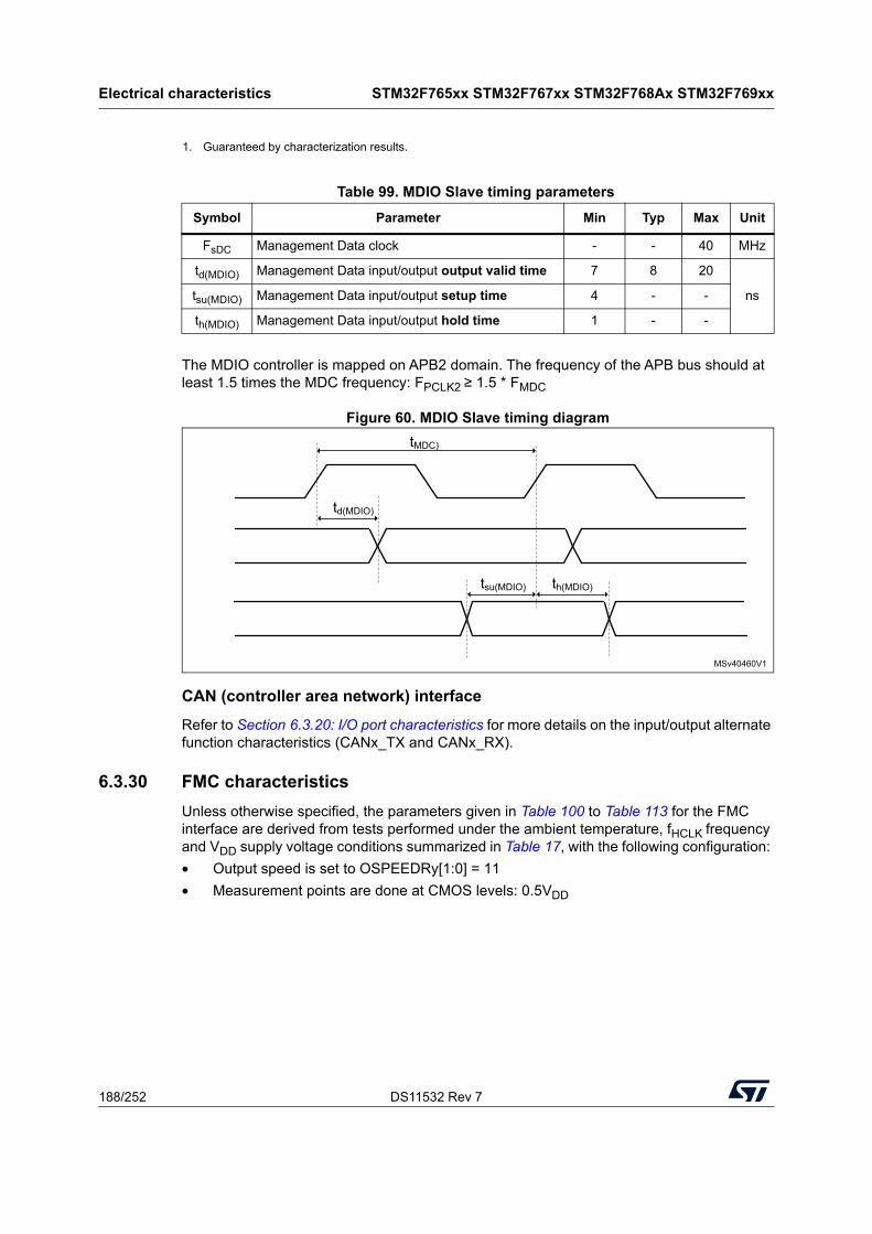
Electrical characteristics STM32F765xx STM32F767xx STM32F768Ax STM32F769xx
188/252 DS11532 Rev 7
The MDIO controller is mapped on APB2 domain. The frequency of the APB bus should at least 1.5 times the MDC frequency: FPCLK2 ≥ 1.5 * FMDC
Figure 60. MDIO Slave timing diagram
CAN (controller area network) interface
Refer to Section 6.3.20: I/O port characteristics for more details on the input/output alternate function characteristics (CANx_TX and CANx_RX).
6.3.30 FMC characteristics
Unless otherwise specified, the parameters given in Table 100 to Table 113 for the FMC interface are derived from tests performed under the ambient temperature, fHCLK frequency and VDD supply voltage conditions summarized in Table 17, with the following configuration:
• Output speed is set to OSPEEDRy[1:0] = 11
• Measurement points are done at CMOS levels: 0.5VDD
1. Guaranteed by characterization results.
Table 99. MDIO Slave timing parameters
Symbol Parameter Min Typ Max Unit
FsDC Management Data clock - - 40 MHz
td(MDIO) Management Data input/output output valid time 7 8 20
nstsu(MDIO) Management Data input/output setup time 4 - -
th(MDIO) Management Data input/output hold time 1 - -
MSv40460V1
tsu(MDIO)
tMDC)
th(MDIO)
td(MDIO)
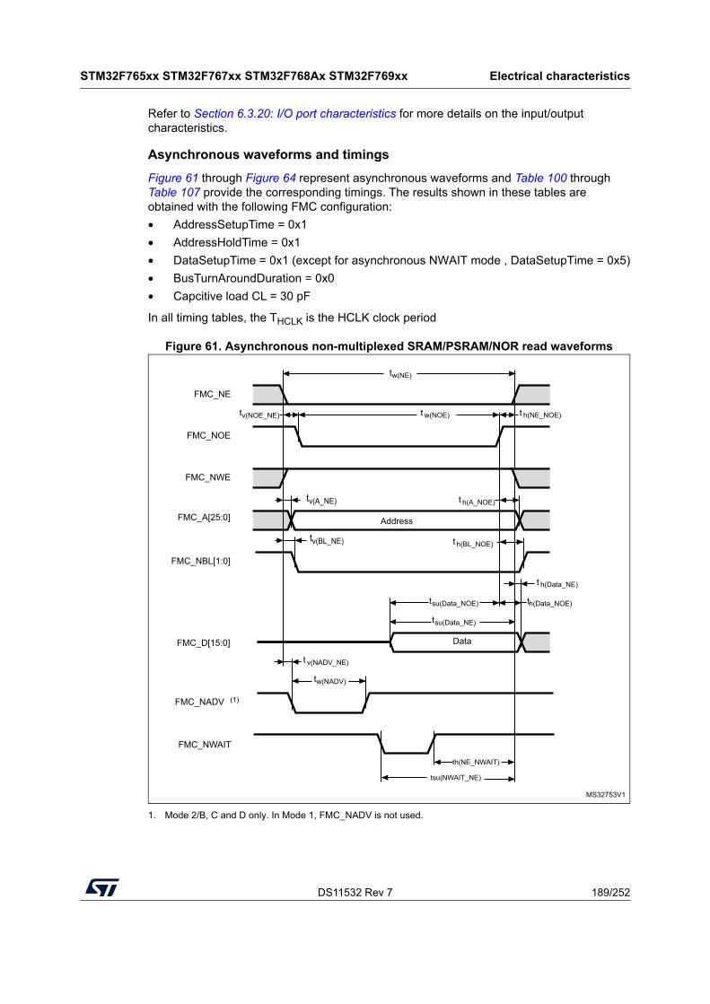
DS11532 Rev 7 189/252
STM32F765xx STM32F767xx STM32F768Ax STM32F769xx Electrical characteristics
218
Refer to Section 6.3.20: I/O port characteristics for more details on the input/output characteristics.
Asynchronous waveforms and timings
Figure 61 through Figure 64 represent asynchronous waveforms and Table 100 through Table 107 provide the corresponding timings. The results shown in these tables are obtained with the following FMC configuration:
• AddressSetupTime = 0x1
• AddressHoldTime = 0x1
• DataSetupTime = 0x1 (except for asynchronous NWAIT mode , DataSetupTime = 0x5)
• BusTurnAroundDuration = 0x0
• Capcitive load CL = 30 pF
In all timing tables, the THCLK is the HCLK clock period
Figure 61. Asynchronous non-multiplexed SRAM/PSRAM/NOR read waveforms
1. Mode 2/B, C and D only. In Mode 1, FMC_NADV is not used.
Data
FMC_NE
FMC_NBL[1:0]
FMC_D[15:0]
tv(BL_NE)
t h(Data_NE)
FMC_NOE
AddressFMC_A[25:0]
tv(A_NE)
FMC_NWE
tsu(Data_NE)
tw(NE)
MS32753V1
w(NOE)ttv(NOE_NE) t h(NE_NOE)
th(Data_NOE)
t h(A_NOE)
t h(BL_NOE)
tsu(Data_NOE)
FMC_NADV (1)
t v(NADV_NE)
tw(NADV)
FMC_NWAIT
tsu(NWAIT_NE)
th(NE_NWAIT)
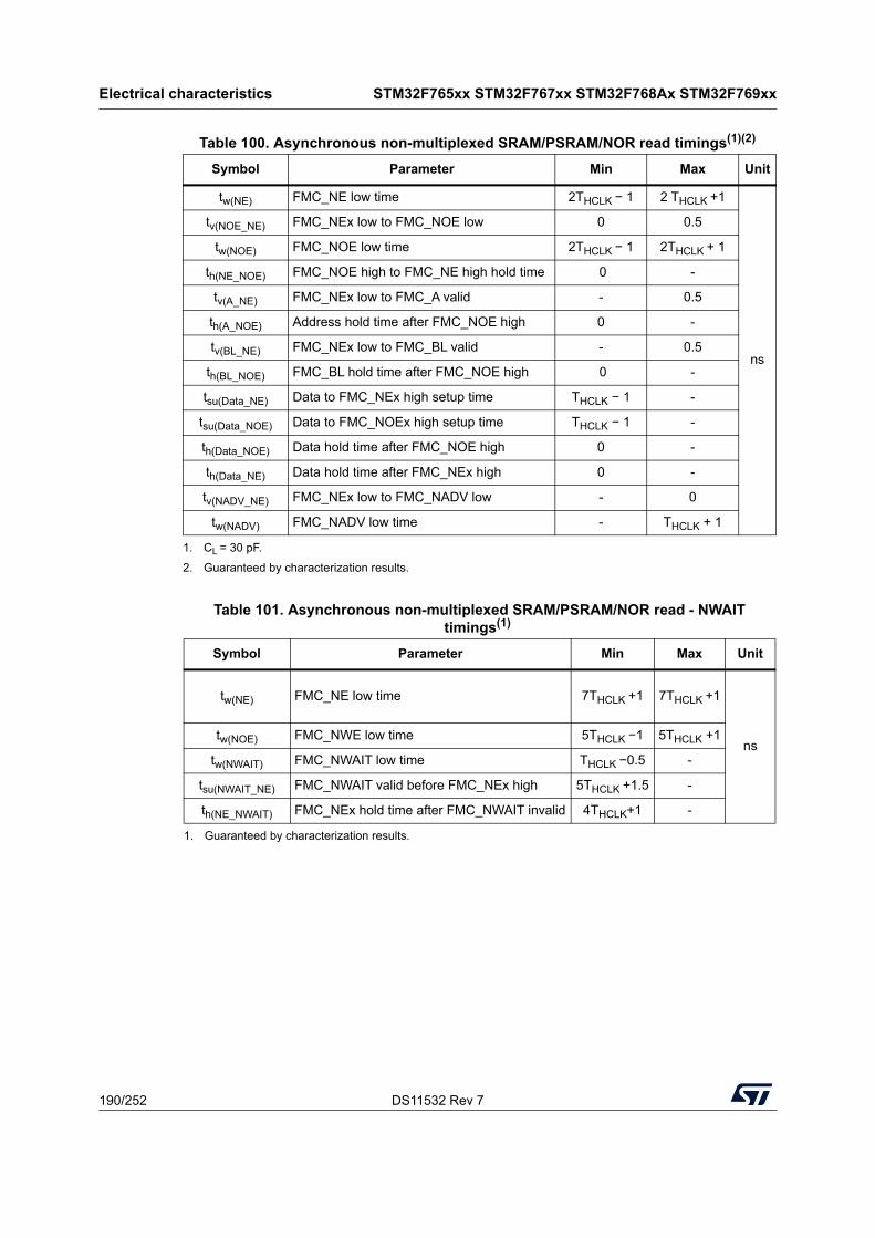
Electrical characteristics STM32F765xx STM32F767xx STM32F768Ax STM32F769xx
190/252 DS11532 Rev 7
Table 100. Asynchronous non-multiplexed SRAM/PSRAM/NOR read timings(1)(2)
1. CL = 30 pF.
2. Guaranteed by characterization results.
Symbol Parameter Min Max Unit
tw(NE) FMC_NE low time 2THCLK − 1 2 THCLK +1
ns
tv(NOE_NE) FMC_NEx low to FMC_NOE low 0 0.5
tw(NOE) FMC_NOE low time 2THCLK − 1 2THCLK + 1
th(NE_NOE) FMC_NOE high to FMC_NE high hold time 0 -
tv(A_NE) FMC_NEx low to FMC_A valid - 0.5
th(A_NOE) Address hold time after FMC_NOE high 0 -
tv(BL_NE) FMC_NEx low to FMC_BL valid - 0.5
th(BL_NOE) FMC_BL hold time after FMC_NOE high 0 -
tsu(Data_NE) Data to FMC_NEx high setup time THCLK − 1 -
tsu(Data_NOE) Data to FMC_NOEx high setup time THCLK − 1 -
th(Data_NOE) Data hold time after FMC_NOE high 0 -
th(Data_NE) Data hold time after FMC_NEx high 0 -
tv(NADV_NE) FMC_NEx low to FMC_NADV low - 0
tw(NADV) FMC_NADV low time - THCLK + 1
Table 101. Asynchronous non-multiplexed SRAM/PSRAM/NOR read - NWAIT timings(1)
1. Guaranteed by characterization results.
Symbol Parameter Min Max Unit
tw(NE) FMC_NE low time 7THCLK +1 7THCLK +1
nstw(NOE) FMC_NWE low time 5THCLK −1 5THCLK +1
tw(NWAIT) FMC_NWAIT low time THCLK −0.5 -
tsu(NWAIT_NE) FMC_NWAIT valid before FMC_NEx high 5THCLK +1.5 -
th(NE_NWAIT) FMC_NEx hold time after FMC_NWAIT invalid 4THCLK+1 -
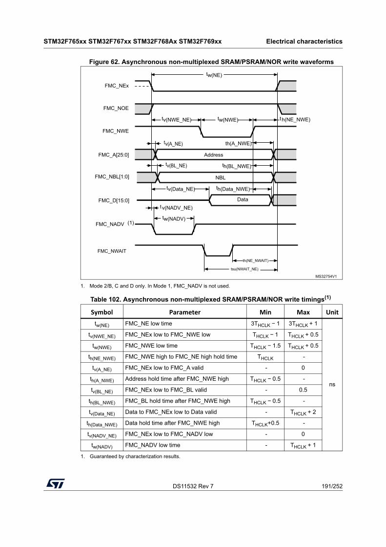
DS11532 Rev 7 191/252
STM32F765xx STM32F767xx STM32F768Ax STM32F769xx Electrical characteristics
218
Figure 62. Asynchronous non-multiplexed SRAM/PSRAM/NOR write waveforms
1. Mode 2/B, C and D only. In Mode 1, FMC_NADV is not used.
Table 102. Asynchronous non-multiplexed SRAM/PSRAM/NOR write timings(1)
1. Guaranteed by characterization results.
Symbol Parameter Min Max Unittw(NE) FMC_NE low time 3THCLK − 1 3THCLK + 1
ns
tv(NWE_NE) FMC_NEx low to FMC_NWE low THCLK − 1 THCLK + 0.5
tw(NWE) FMC_NWE low time THCLK − 1.5 THCLK + 0.5
th(NE_NWE) FMC_NWE high to FMC_NE high hold time THCLK -
tv(A_NE) FMC_NEx low to FMC_A valid - 0
th(A_NWE) Address hold time after FMC_NWE high THCLK − 0.5 -
tv(BL_NE) FMC_NEx low to FMC_BL valid - 0.5
th(BL_NWE) FMC_BL hold time after FMC_NWE high THCLK − 0.5 -
tv(Data_NE) Data to FMC_NEx low to Data valid - THCLK + 2
th(Data_NWE) Data hold time after FMC_NWE high THCLK+0.5 -
tv(NADV_NE) FMC_NEx low to FMC_NADV low - 0
tw(NADV) FMC_NADV low time - THCLK + 1
NBL
Data
FMC_NEx
FMC_NBL[1:0]
FMC_D[15:0]
tv(BL_NE)
th(Data_NWE)
FMC_NOE
AddressFMC_A[25:0]
tv(A_NE)
tw(NWE)
FMC_NWE
tv(NWE_NE) th(NE_NWE)
th(A_NWE)
th(BL_NWE)
tv(Data_NE)
tw(NE)
MS32754V1
FMC_NADV (1)
tv(NADV_NE)
tw(NADV)
FMC_NWAIT
tsu(NWAIT_NE)
th(NE_NWAIT)
Electrical characteristics STM32F765xx STM32F767xx STM32F768Ax STM32F769xx
192/252 DS11532 Rev 7
Figure 63. Asynchronous multiplexed PSRAM/NOR read waveforms
Table 103. Asynchronous non-multiplexed SRAM/PSRAM/NOR write - NWAIT timings(1)
1. Guaranteed by characterization results.
Symbol Parameter Min Max Unit
tw(NE) FMC_NE low time 8THCLK − 1 8THCLK + 1
nstw(NWE) FMC_NWE low time 6THCLK − 1.5 6THCLK + 0.5
tsu(NWAIT_NE) FMC_NWAIT valid before FMC_NEx high 6THCLK − 1 -
th(NE_NWAIT)FMC_NEx hold time after FMC_NWAIT invalid
4THCLK + 2 -
NBL
Data
FMC_ NBL[1:0]
FMC_ AD[15:0]
tv(BL_NE)
th(Data_NE)
AddressFMC_ A[25:16]
tv(A_NE)
FMC_NWE
tv(A_NE)
MS32755V1
Address
FMC_NADV
tv(NADV_NE)tw(NADV)
tsu(Data_NE)
th(AD_NADV)
FMC_ NE
FMC_NOE
tw(NE)
tw(NOE)
tv(NOE_NE) th(NE_NOE)
th(A_NOE)
th(BL_NOE)
tsu(Data_NOE) th(Data_NOE)
FMC_NWAIT
tsu(NWAIT_NE)
th(NE_NWAIT)
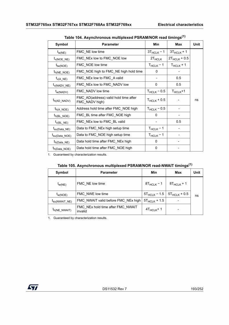
DS11532 Rev 7 193/252
STM32F765xx STM32F767xx STM32F768Ax STM32F769xx Electrical characteristics
218
Table 104. Asynchronous multiplexed PSRAM/NOR read timings(1)
1. Guaranteed by characterization results.
Symbol Parameter Min Max Unit
tw(NE) FMC_NE low time 3THCLK − 1 3THCLK + 1
ns
tv(NOE_NE) FMC_NEx low to FMC_NOE low 2THCLK 2THCLK + 0.5
ttw(NOE) FMC_NOE low time THCLK − 1 THCLK + 1
th(NE_NOE) FMC_NOE high to FMC_NE high hold time 0 -
tv(A_NE) FMC_NEx low to FMC_A valid - 0.5
tv(NADV_NE) FMC_NEx low to FMC_NADV low 0 0.5
tw(NADV) FMC_NADV low time THCLK − 0.5 THCLK+1
th(AD_NADV)FMC_AD(address) valid hold time after FMC_NADV high)
THCLK + 0.5 -
th(A_NOE) Address hold time after FMC_NOE high THCLK − 0.5 -
th(BL_NOE) FMC_BL time after FMC_NOE high 0 -
tv(BL_NE) FMC_NEx low to FMC_BL valid - 0.5
tsu(Data_NE) Data to FMC_NEx high setup time THCLK − 1 -
tsu(Data_NOE) Data to FMC_NOE high setup time THCLK − 1 -
th(Data_NE) Data hold time after FMC_NEx high 0 -
th(Data_NOE) Data hold time after FMC_NOE high 0 -
Table 105. Asynchronous multiplexed PSRAM/NOR read-NWAIT timings(1)
1. Guaranteed by characterization results.
Symbol Parameter Min Max Unit
tw(NE) FMC_NE low time 8THCLK − 1 8THCLK + 1
nstw(NOE) FMC_NWE low time 5THCLK − 1.5 5THCLK + 0.5
tsu(NWAIT_NE) FMC_NWAIT valid before FMC_NEx high 5THCLK + 1.5 -
th(NE_NWAIT)FMC_NEx hold time after FMC_NWAIT invalid
4THCLK+ 1 -
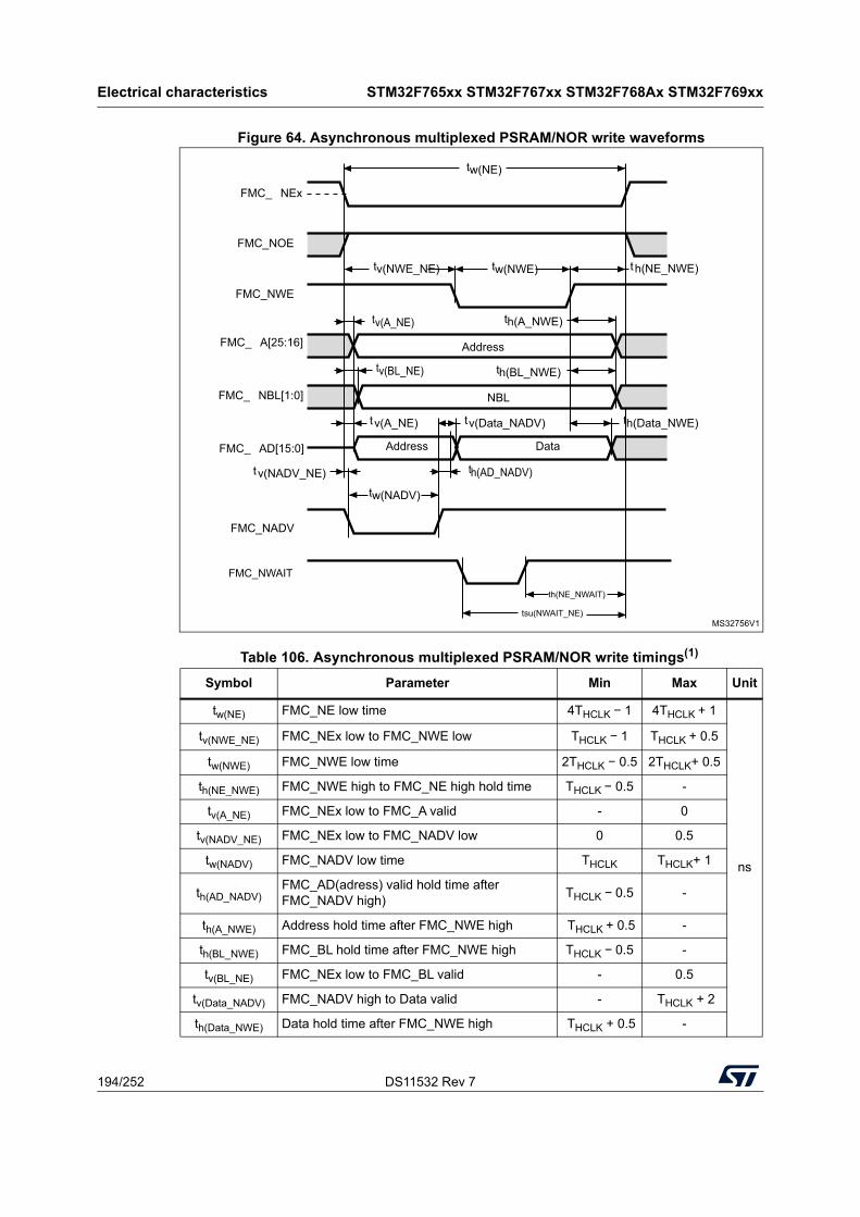
Electrical characteristics STM32F765xx STM32F767xx STM32F768Ax STM32F769xx
194/252 DS11532 Rev 7
Figure 64. Asynchronous multiplexed PSRAM/NOR write waveforms
Table 106. Asynchronous multiplexed PSRAM/NOR write timings(1)
Symbol Parameter Min Max Unit
tw(NE) FMC_NE low time 4THCLK − 1 4THCLK + 1
ns
tv(NWE_NE) FMC_NEx low to FMC_NWE low THCLK − 1 THCLK + 0.5
tw(NWE) FMC_NWE low time 2THCLK − 0.5 2THCLK+ 0.5
th(NE_NWE) FMC_NWE high to FMC_NE high hold time THCLK − 0.5 -
tv(A_NE) FMC_NEx low to FMC_A valid - 0
tv(NADV_NE) FMC_NEx low to FMC_NADV low 0 0.5
tw(NADV) FMC_NADV low time THCLK THCLK+ 1
th(AD_NADV)FMC_AD(adress) valid hold time after FMC_NADV high)
THCLK − 0.5 -
th(A_NWE) Address hold time after FMC_NWE high THCLK + 0.5 -
th(BL_NWE) FMC_BL hold time after FMC_NWE high THCLK − 0.5 -
tv(BL_NE) FMC_NEx low to FMC_BL valid - 0.5
tv(Data_NADV) FMC_NADV high to Data valid - THCLK + 2
th(Data_NWE) Data hold time after FMC_NWE high THCLK + 0.5 -
NBL
Data
FMC_ NEx
FMC_ NBL[1:0]
FMC_ AD[15:0]
tv(BL_NE)
th(Data_NWE)
FMC_NOE
AddressFMC_ A[25:16]
tv(A_NE)
tw(NWE)
FMC_NWE
tv(NWE_NE) th(NE_NWE)
th(A_NWE)
th(BL_NWE)
tv(A_NE)
tw(NE)
MS32756V1
Address
FMC_NADV
tv(NADV_NE)
tw(NADV)
tv(Data_NADV)
th(AD_NADV)
FMC_NWAIT
tsu(NWAIT_NE)
th(NE_NWAIT)
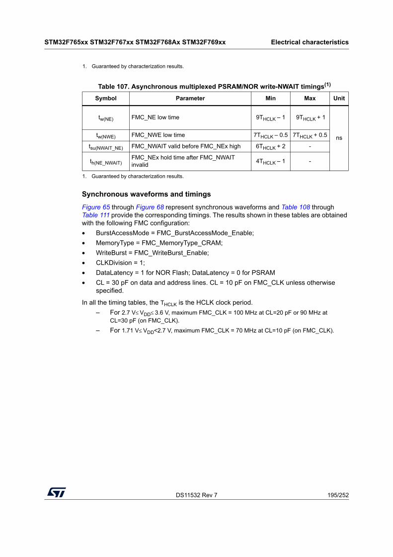
DS11532 Rev 7 195/252
STM32F765xx STM32F767xx STM32F768Ax STM32F769xx Electrical characteristics
218
Synchronous waveforms and timings
Figure 65 through Figure 68 represent synchronous waveforms and Table 108 through Table 111 provide the corresponding timings. The results shown in these tables are obtained with the following FMC configuration:
• BurstAccessMode = FMC_BurstAccessMode_Enable;
• MemoryType = FMC_MemoryType_CRAM;
• WriteBurst = FMC_WriteBurst_Enable;
• CLKDivision = 1;
• DataLatency = 1 for NOR Flash; DataLatency = 0 for PSRAM
• CL = 30 pF on data and address lines. CL = 10 pF on FMC_CLK unless otherwise specified.
In all the timing tables, the THCLK is the HCLK clock period.
– For 2.7 V≤ VDD≤ 3.6 V, maximum FMC_CLK = 100 MHz at CL=20 pF or 90 MHz at CL=30 pF (on FMC_CLK).
– For 1.71 V≤ VDD<2.7 V, maximum FMC_CLK = 70 MHz at CL=10 pF (on FMC_CLK).
1. Guaranteed by characterization results.
Table 107. Asynchronous multiplexed PSRAM/NOR write-NWAIT timings(1)
1. Guaranteed by characterization results.
Symbol Parameter Min Max Unit
tw(NE) FMC_NE low time 9THCLK – 1 9THCLK + 1
nstw(NWE) FMC_NWE low time 7THCLK – 0.5 7THCLK + 0.5
tsu(NWAIT_NE) FMC_NWAIT valid before FMC_NEx high 6THCLK + 2 -
th(NE_NWAIT)FMC_NEx hold time after FMC_NWAIT invalid
4THCLK – 1 -
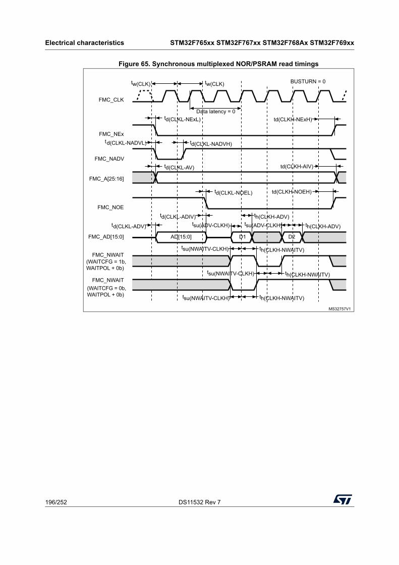
Electrical characteristics STM32F765xx STM32F767xx STM32F768Ax STM32F769xx
196/252 DS11532 Rev 7
Figure 65. Synchronous multiplexed NOR/PSRAM read timings
FMC_CLK
FMC_NEx
FMC_NADV
FMC_A[25:16]
FMC_NOE
FMC_AD[15:0] AD[15:0] D1 D2
FMC_NWAIT(WAITCFG = 1b, WAITPOL + 0b)
FMC_NWAIT(WAITCFG = 0b, WAITPOL + 0b)
tw(CLK) tw(CLK)
Data latency = 0
BUSTURN = 0
td(CLKL-NExL) td(CLKH-NExH)
td(CLKL-NADVL)
td(CLKL-AV)
td(CLKL-NADVH)
td(CLKH-AIV)
td(CLKL-NOEL) td(CLKH-NOEH)
td(CLKL-ADV)
td(CLKL-ADIV)tsu(ADV-CLKH)
th(CLKH-ADV)tsu(ADV-CLKH) th(CLKH-ADV)
tsu(NWAITV-CLKH) th(CLKH-NWAITV)
tsu(NWAITV-CLKH) th(CLKH-NWAITV)
tsu(NWAITV-CLKH) th(CLKH-NWAITV)
MS32757V1
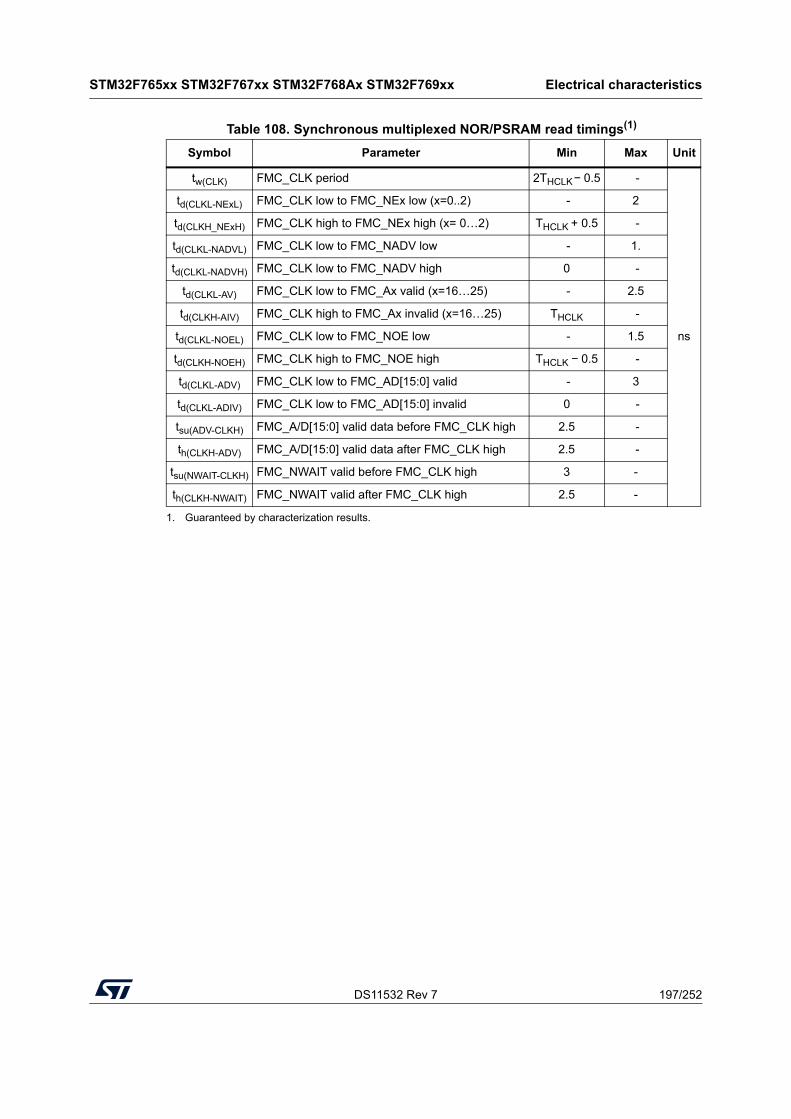
DS11532 Rev 7 197/252
STM32F765xx STM32F767xx STM32F768Ax STM32F769xx Electrical characteristics
218
Table 108. Synchronous multiplexed NOR/PSRAM read timings(1)
1. Guaranteed by characterization results.
Symbol Parameter Min Max Unit
tw(CLK) FMC_CLK period 2THCLK− 0.5 -
ns
td(CLKL-NExL) FMC_CLK low to FMC_NEx low (x=0..2) - 2
td(CLKH_NExH) FMC_CLK high to FMC_NEx high (x= 0…2) THCLK + 0.5 -
td(CLKL-NADVL) FMC_CLK low to FMC_NADV low - 1.
td(CLKL-NADVH) FMC_CLK low to FMC_NADV high 0 -
td(CLKL-AV) FMC_CLK low to FMC_Ax valid (x=16…25) - 2.5
td(CLKH-AIV) FMC_CLK high to FMC_Ax invalid (x=16…25) THCLK -
td(CLKL-NOEL) FMC_CLK low to FMC_NOE low - 1.5
td(CLKH-NOEH) FMC_CLK high to FMC_NOE high THCLK − 0.5 -
td(CLKL-ADV) FMC_CLK low to FMC_AD[15:0] valid - 3
td(CLKL-ADIV) FMC_CLK low to FMC_AD[15:0] invalid 0 -
tsu(ADV-CLKH) FMC_A/D[15:0] valid data before FMC_CLK high 2.5 -
th(CLKH-ADV) FMC_A/D[15:0] valid data after FMC_CLK high 2.5 -
tsu(NWAIT-CLKH) FMC_NWAIT valid before FMC_CLK high 3 -
th(CLKH-NWAIT) FMC_NWAIT valid after FMC_CLK high 2.5 -
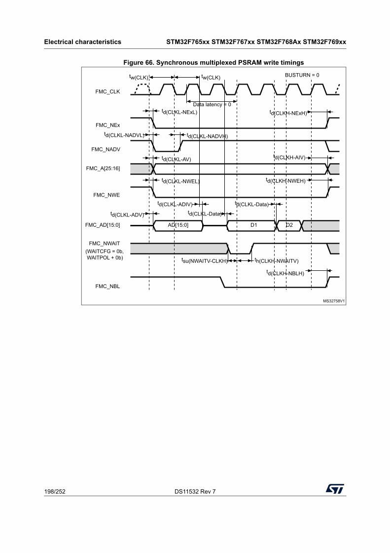
Electrical characteristics STM32F765xx STM32F767xx STM32F768Ax STM32F769xx
198/252 DS11532 Rev 7
Figure 66. Synchronous multiplexed PSRAM write timings
FMC_CLK
FMC_NEx
FMC_NADV
FMC_A[25:16]
FMC_NWE
FMC_AD[15:0] AD[15:0] D1 D2
FMC_NWAIT(WAITCFG = 0b, WAITPOL + 0b)
tw(CLK) tw(CLK)
Data latency = 0
BUSTURN = 0
td(CLKL-NExL) td(CLKH-NExH)
td(CLKL-NADVL)
td(CLKL-AV)
td(CLKL-NADVH)
td(CLKH-AIV)
td(CLKH-NWEH)td(CLKL-NWEL)
td(CLKH-NBLH)
td(CLKL-ADV)
td(CLKL-ADIV) td(CLKL-Data)
tsu(NWAITV-CLKH) th(CLKH-NWAITV)
MS32758V1
td(CLKL-Data)
FMC_NBL
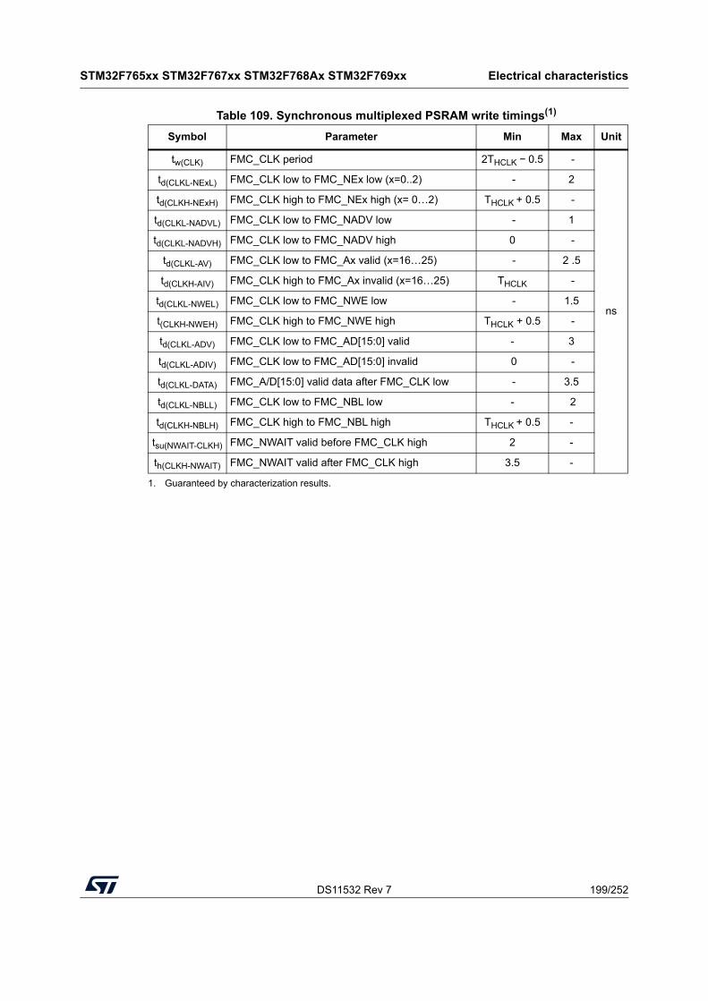
DS11532 Rev 7 199/252
STM32F765xx STM32F767xx STM32F768Ax STM32F769xx Electrical characteristics
218
Table 109. Synchronous multiplexed PSRAM write timings(1)
1. Guaranteed by characterization results.
Symbol Parameter Min Max Unit
tw(CLK) FMC_CLK period 2THCLK − 0.5 -
ns
td(CLKL-NExL) FMC_CLK low to FMC_NEx low (x=0..2) - 2
td(CLKH-NExH) FMC_CLK high to FMC_NEx high (x= 0…2) THCLK + 0.5 -
td(CLKL-NADVL) FMC_CLK low to FMC_NADV low - 1
td(CLKL-NADVH) FMC_CLK low to FMC_NADV high 0 -
td(CLKL-AV) FMC_CLK low to FMC_Ax valid (x=16…25) - 2 .5
td(CLKH-AIV) FMC_CLK high to FMC_Ax invalid (x=16…25) THCLK -
td(CLKL-NWEL) FMC_CLK low to FMC_NWE low - 1.5
t(CLKH-NWEH) FMC_CLK high to FMC_NWE high THCLK + 0.5 -
td(CLKL-ADV) FMC_CLK low to FMC_AD[15:0] valid - 3
td(CLKL-ADIV) FMC_CLK low to FMC_AD[15:0] invalid 0 -
td(CLKL-DATA) FMC_A/D[15:0] valid data after FMC_CLK low - 3.5
td(CLKL-NBLL) FMC_CLK low to FMC_NBL low - 2
td(CLKH-NBLH) FMC_CLK high to FMC_NBL high THCLK + 0.5 -
tsu(NWAIT-CLKH) FMC_NWAIT valid before FMC_CLK high 2 -
th(CLKH-NWAIT) FMC_NWAIT valid after FMC_CLK high 3.5 -
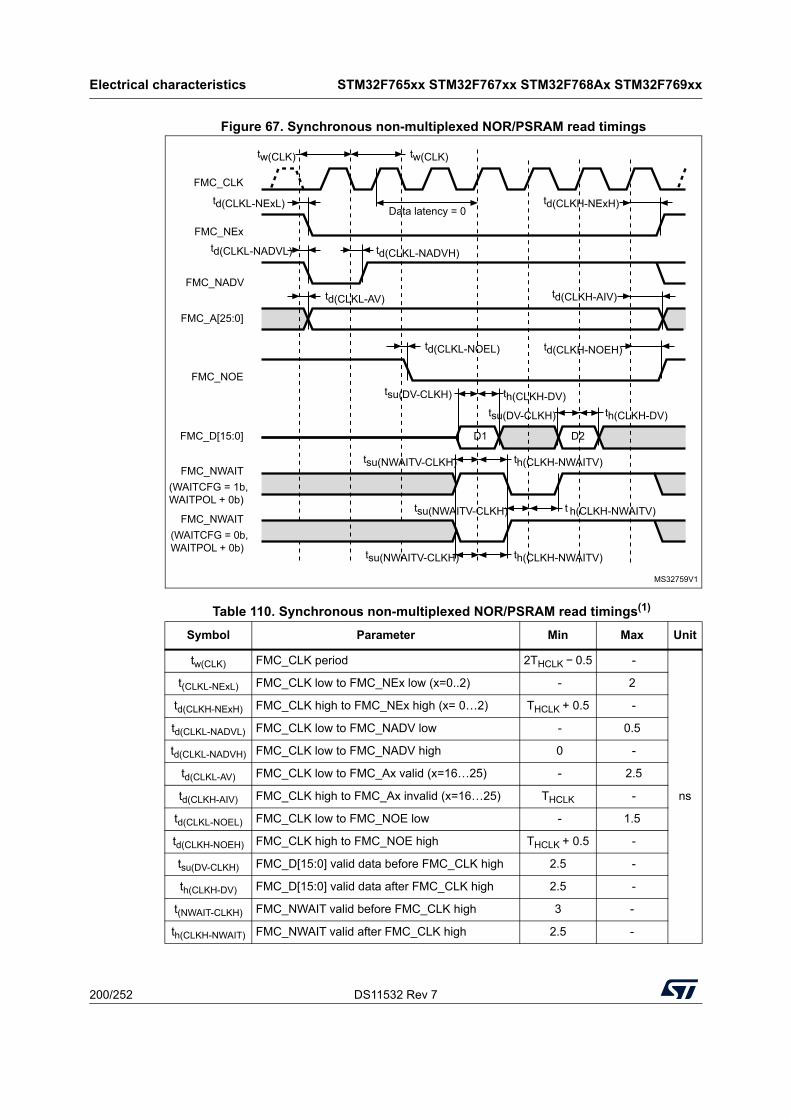
Electrical characteristics STM32F765xx STM32F767xx STM32F768Ax STM32F769xx
200/252 DS11532 Rev 7
Figure 67. Synchronous non-multiplexed NOR/PSRAM read timings
Table 110. Synchronous non-multiplexed NOR/PSRAM read timings(1)
Symbol Parameter Min Max Unit
tw(CLK) FMC_CLK period 2THCLK − 0.5 -
ns
t(CLKL-NExL) FMC_CLK low to FMC_NEx low (x=0..2) - 2
td(CLKH-NExH) FMC_CLK high to FMC_NEx high (x= 0…2) THCLK + 0.5 -
td(CLKL-NADVL) FMC_CLK low to FMC_NADV low - 0.5
td(CLKL-NADVH) FMC_CLK low to FMC_NADV high 0 -
td(CLKL-AV) FMC_CLK low to FMC_Ax valid (x=16…25) - 2.5
td(CLKH-AIV) FMC_CLK high to FMC_Ax invalid (x=16…25) THCLK -
td(CLKL-NOEL) FMC_CLK low to FMC_NOE low - 1.5
td(CLKH-NOEH) FMC_CLK high to FMC_NOE high THCLK + 0.5 -
tsu(DV-CLKH) FMC_D[15:0] valid data before FMC_CLK high 2.5 -
th(CLKH-DV) FMC_D[15:0] valid data after FMC_CLK high 2.5 -
t(NWAIT-CLKH) FMC_NWAIT valid before FMC_CLK high 3 -
th(CLKH-NWAIT) FMC_NWAIT valid after FMC_CLK high 2.5 -
FMC_CLK
FMC_NEx
FMC_A[25:0]
FMC_NOE
FMC_D[15:0] D1 D2
FMC_NWAIT(WAITCFG = 1b, WAITPOL + 0b)
FMC_NWAIT(WAITCFG = 0b, WAITPOL + 0b)
tw(CLK) tw(CLK)
Data latency = 0td(CLKL-NExL) td(CLKH-NExH)
td(CLKL-AV) td(CLKH-AIV)
td(CLKL-NOEL) td(CLKH-NOEH)
tsu(DV-CLKH) th(CLKH-DV)tsu(DV-CLKH) th(CLKH-DV)
tsu(NWAITV-CLKH) th(CLKH-NWAITV)
tsu(NWAITV-CLKH) t h(CLKH-NWAITV)
tsu(NWAITV-CLKH) th(CLKH-NWAITV)
MS32759V1
FMC_NADV
td(CLKL-NADVL) td(CLKL-NADVH)
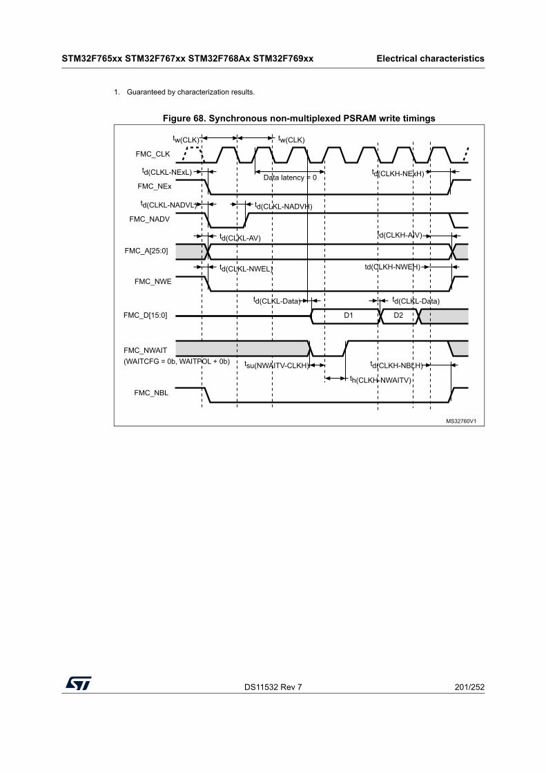
DS11532 Rev 7 201/252
STM32F765xx STM32F767xx STM32F768Ax STM32F769xx Electrical characteristics
218
Figure 68. Synchronous non-multiplexed PSRAM write timings
1. Guaranteed by characterization results.
MS32760V1
FMC_CLK
FMC_NEx
FMC_A[25:0]
FMC_NWE
FMC_D[15:0] D1 D2
FMC_NWAIT(WAITCFG = 0b, WAITPOL + 0b)
tw(CLK) tw(CLK)
Data latency = 0td(CLKL-NExL) td(CLKH-NExH)
td(CLKL-AV)td(CLKH-AIV)
td(CLKH-NWEH)td(CLKL-NWEL)
td(CLKL-Data)
tsu(NWAITV-CLKH)
th(CLKH-NWAITV)
FMC_NADV
td(CLKL-NADVL) td(CLKL-NADVH)
td(CLKL-Data)
FMC_NBL
td(CLKH-NBLH)
Electrical characteristics STM32F765xx STM32F767xx STM32F768Ax STM32F769xx
202/252 DS11532 Rev 7
NAND controller waveforms and timings
Figure 69 through Figure 72 represent synchronous waveforms, and Table 112 and Table 113 provide the corresponding timings. The results shown in this table are obtained with the following FMC configuration:
• COM.FMC_SetupTime = 0x01;
• COM.FMC_WaitSetupTime = 0x03;
• COM.FMC_HoldSetupTime = 0x02;
• COM.FMC_HiZSetupTime = 0x01;
• ATT.FMC_SetupTime = 0x01;
• ATT.FMC_WaitSetupTime = 0x03;
• ATT.FMC_HoldSetupTime = 0x02;
• ATT.FMC_HiZSetupTime = 0x01;
• Bank = FMC_Bank_NAND;
• MemoryDataWidth = FMC_MemoryDataWidth_16b;
• ECC = FMC_ECC_Enable;
• ECCPageSize = FMC_ECCPageSize_512Bytes;
• TCLRSetupTime = 0;
• TARSetupTime = 0.
In all timing tables, the THCLK is the HCLK clock period.
Table 111. Synchronous non-multiplexed PSRAM write timings(1)
1. Guaranteed by characterization results.
Symbol Parameter Min Max Unit
t(CLK) FMC_CLK period 2THCLK − 0.5 -
ns
td(CLKL-NExL) FMC_CLK low to FMC_NEx low (x=0..2) - 2
t(CLKH-NExH) FMC_CLK high to FMC_NEx high (x= 0…2) THCLK + 0.5 -
td(CLKL-NADVL) FMC_CLK low to FMC_NADV low - 0.5
td(CLKL-NADVH) FMC_CLK low to FMC_NADV high 0 -
td(CLKL-AV) FMC_CLK low to FMC_Ax valid (x=16…25) - 2.5
td(CLKH-AIV) FMC_CLK high to FMC_Ax invalid (x=16…25) THCLK -
td(CLKL-NWEL) FMC_CLK low to FMC_NWE low - 1.5
td(CLKH-NWEH) FMC_CLK high to FMC_NWE high THCLK + 1 -
td(CLKL-Data) FMC_D[15:0] valid data after FMC_CLK low - 3.5
td(CLKL-NBLL) FMC_CLK low to FMC_NBL low - 2
td(CLKH-NBLH) FMC_CLK high to FMC_NBL high THCLK + 1 -
tsu(NWAIT-CLKH) FMC_NWAIT valid before FMC_CLK high 2 -
th(CLKH-NWAIT) FMC_NWAIT valid after FMC_CLK high 3.5 -
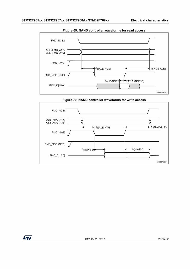
DS11532 Rev 7 203/252
STM32F765xx STM32F767xx STM32F768Ax STM32F769xx Electrical characteristics
218
Figure 69. NAND controller waveforms for read access
Figure 70. NAND controller waveforms for write access
FMC_NWE
FMC_NOE (NRE)
FMC_D[15:0]
tsu(D-NOE) th(NOE-D)
MS32767V1
ALE (FMC_A17)CLE (FMC_A16)
FMC_NCEx
td(ALE-NOE) th(NOE-ALE)
MS32768V1
th(NWE-D)tv(NWE-D)
FMC_NWE
FMC_NOE (NRE)
FMC_D[15:0]
ALE (FMC_A17)CLE (FMC_A16)
FMC_NCEx
td(ALE-NWE) th(NWE-ALE)
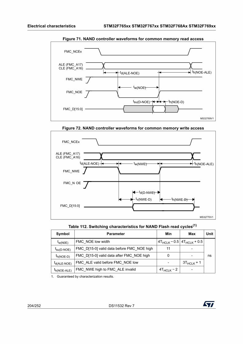
Electrical characteristics STM32F765xx STM32F767xx STM32F768Ax STM32F769xx
204/252 DS11532 Rev 7
Figure 71. NAND controller waveforms for common memory read access
Figure 72. NAND controller waveforms for common memory write access
Table 112. Switching characteristics for NAND Flash read cycles(1)
1. Guaranteed by characterization results.
Symbol Parameter Min Max Unit
tw(N0E) FMC_NOE low width 4THCLK − 0.5 4THCLK + 0.5
ns
tsu(D-NOE) FMC_D[15-0] valid data before FMC_NOE high 11 -
th(NOE-D) FMC_D[15-0] valid data after FMC_NOE high 0 -
td(ALE-NOE) FMC_ALE valid before FMC_NOE low - 3THCLK + 1
th(NOE-ALE) FMC_NWE high to FMC_ALE invalid 4THCLK − 2 -
MS32769V1
FMC_NWE
FMC_NOE
FMC_D[15:0]
tw(NOE)
tsu(D-NOE) th(NOE-D)
ALE (FMC_A17)CLE (FMC_A16)
FMC_NCEx
td(ALE-NOE) th(NOE-ALE)
MS32770V1
tw(NWE)
th(NWE-D)tv(NWE-D)
FMC_NWE
FMC_N OE
FMC_D[15:0]
td(D-NWE)
ALE (FMC_A17)CLE (FMC_A16)
FMC_NCEx
td(ALE-NOE) th(NOE-ALE)
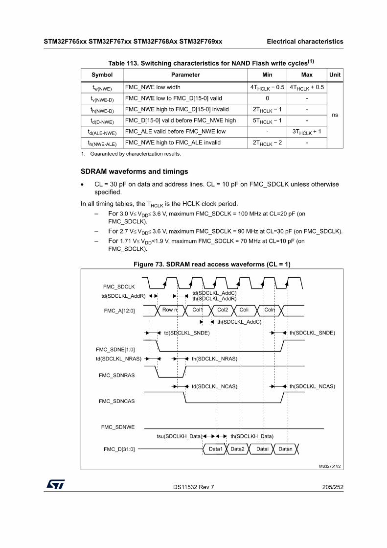
DS11532 Rev 7 205/252
STM32F765xx STM32F767xx STM32F768Ax STM32F769xx Electrical characteristics
218
SDRAM waveforms and timings
• CL = 30 pF on data and address lines. CL = 10 pF on FMC_SDCLK unless otherwise specified.
In all timing tables, the THCLK is the HCLK clock period.
– For 3.0 V≤ VDD≤ 3.6 V, maximum FMC_SDCLK = 100 MHz at CL=20 pF (on FMC_SDCLK).
– For 2.7 V≤ VDD≤ 3.6 V, maximum FMC_SDCLK = 90 MHz at CL=30 pF (on FMC_SDCLK).
– For 1.71 V≤ VDD<1.9 V, maximum FMC_SDCLK = 70 MHz at CL=10 pF (on FMC_SDCLK).
Figure 73. SDRAM read access waveforms (CL = 1)
Table 113. Switching characteristics for NAND Flash write cycles(1)
1. Guaranteed by characterization results.
Symbol Parameter Min Max Unit
tw(NWE) FMC_NWE low width 4THCLK − 0.5 4THCLK + 0.5
ns
tv(NWE-D) FMC_NWE low to FMC_D[15-0] valid 0 -
th(NWE-D) FMC_NWE high to FMC_D[15-0] invalid 2THCLK − 1 -
td(D-NWE) FMC_D[15-0] valid before FMC_NWE high 5THCLK − 1 -
td(ALE-NWE) FMC_ALE valid before FMC_NWE low - 3THCLK + 1
th(NWE-ALE) FMC_NWE high to FMC_ALE invalid 2THCLK − 2 -
MS32751V2
Row n Col1
FMC_SDCLK
FMC_A[12:0]
FMC_SDNRAS
FMC_SDNCAS
FMC_SDNWE
FMC_D[31:0]
FMC_SDNE[1:0]
td(SDCLKL_AddR) td(SDCLKL_AddC)th(SDCLKL_AddR)
th(SDCLKL_AddC)
td(SDCLKL_SNDE)
tsu(SDCLKH_Data) th(SDCLKH_Data)
Col2 Coli Coln
Data2 Datai DatanData1
th(SDCLKL_SNDE)
td(SDCLKL_NRAS)
td(SDCLKL_NCAS) th(SDCLKL_NCAS)
th(SDCLKL_NRAS)

Electrical characteristics STM32F765xx STM32F767xx STM32F768Ax STM32F769xx
206/252 DS11532 Rev 7
Table 114. SDRAM read timings(1)
1. Guaranteed by characterization results.
Symbol Parameter Min Max Unit
tw(SDCLK) FMC_SDCLK period 2THCLK − 0.5 2THCLK + 0.5
ns
tsu(SDCLKH _Data) Data input setup time 2.5 -
th(SDCLKH_Data) Data input hold time 0.5 -
td(SDCLKL_Add) Address valid time - 3.5
td(SDCLKL- SDNE) Chip select valid time - 1.5
th(SDCLKL_SDNE) Chip select hold time 0.5 -
td(SDCLKL_SDNRAS) SDNRAS valid time - 1
th(SDCLKL_SDNRAS) SDNRAS hold time 0.5 -
td(SDCLKL_SDNCAS) SDNCAS valid time - 0.5
th(SDCLKL_SDNCAS) SDNCAS hold time 0 -
Table 115. LPSDR SDRAM read timings(1)
1. Guaranteed by characterization results.
Symbol Parameter Min Max Unit
tW(SDCLK) FMC_SDCLK period 2THCLK − 0.5 2THCLK + 0.5
ns
tsu(SDCLKH_Data) Data input setup time 1 -
th(SDCLKH_Data) Data input hold time 3.5 -
td(SDCLKL_Add) Address valid time - 2.5
td(SDCLKL_SDNE) Chip select valid time - 2.5
th(SDCLKL_SDNE) Chip select hold time 0 -
td(SDCLKL_SDNRAS SDNRAS valid time - 0.5
th(SDCLKL_SDNRAS) SDNRAS hold time 0 -
td(SDCLKL_SDNCAS) SDNCAS valid time - 1.5
th(SDCLKL_SDNCAS) SDNCAS hold time 0 -
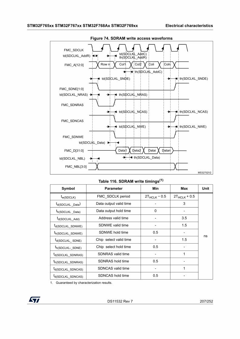
DS11532 Rev 7 207/252
STM32F765xx STM32F767xx STM32F768Ax STM32F769xx Electrical characteristics
218
Figure 74. SDRAM write access waveforms
Table 116. SDRAM write timings(1)
1. Guaranteed by characterization results.
Symbol Parameter Min Max Unit
tw(SDCLK) FMC_SDCLK period 2THCLK − 0.5 2THCLK + 0.5
ns
td(SDCLKL _Data) Data output valid time - 3
th(SDCLKL _Data) Data output hold time 0 -
td(SDCLKL_Add) Address valid time - 3.5
td(SDCLKL_SDNWE) SDNWE valid time - 1.5
th(SDCLKL_SDNWE) SDNWE hold time 0.5 -
td(SDCLKL_ SDNE) Chip select valid time - 1.5
th(SDCLKL-_SDNE) Chip select hold time 0.5 -
td(SDCLKL_SDNRAS) SDNRAS valid time - 1
th(SDCLKL_SDNRAS) SDNRAS hold time 0.5 -
td(SDCLKL_SDNCAS) SDNCAS valid time - 1
td(SDCLKL_SDNCAS) SDNCAS hold time 0.5 -
MS32752V2
Row n Col1
FMC_SDCLK
FMC_A[12:0]
FMC_SDNRAS
FMC_SDNCAS
FMC_SDNWE
FMC_D[31:0]
FMC_SDNE[1:0]
td(SDCLKL_AddR) td(SDCLKL_AddC)th(SDCLKL_AddR)
th(SDCLKL_AddC)
td(SDCLKL_SNDE)
td(SDCLKL_Data)
th(SDCLKL_Data)
Col2 Coli Coln
Data2 Datai DatanData1
th(SDCLKL_SNDE)
td(SDCLKL_NRAS)
td(SDCLKL_NCAS) th(SDCLKL_NCAS)
th(SDCLKL_NRAS)
td(SDCLKL_NWE) th(SDCLKL_NWE)
FMC_NBL[3:0]
td(SDCLKL_NBL)
Electrical characteristics STM32F765xx STM32F767xx STM32F768Ax STM32F769xx
208/252 DS11532 Rev 7
6.3.31 Quad-SPI interface characteristics
Unless otherwise specified, the parameters given in Table 118 and Table 119 for Quad-SPI are derived from tests performed under the ambient temperature, fAHB frequency and VDD
supply voltage conditions summarized in Table 17: General operating conditions, with the following configuration:• Output speed is set to OSPEEDRy[1:0] = 11
• Capacitive load C = 20 pF
• Measurement points are done at CMOS levels: 0.5 ₓ VDD
Refer to Section 6.3.20: I/O port characteristics for more details on the input/output alternate function characteristics.
Table 117. LPSDR SDRAM write timings(1)
1. Guaranteed by characterization results.
Symbol Parameter Min Max Unit
tw(SDCLK) FMC_SDCLK period 2THCLK − 0.5 2THCLK + 0.5
ns
td(SDCLKL _Data) Data output valid time - 2.5
th(SDCLKL _Data) Data output hold time 0 -
td(SDCLKL_Add) Address valid time - 2.5
td(SDCLKL-SDNWE) SDNWE valid time - 2.5
th(SDCLKL-SDNWE) SDNWE hold time 0 -
td(SDCLKL- SDNE) Chip select valid time - 0.5
th(SDCLKL- SDNE) Chip select hold time 0 -
td(SDCLKL-SDNRAS) SDNRAS valid time - 1.5
th(SDCLKL-SDNRAS) SDNRAS hold time 0 -
td(SDCLKL-SDNCAS) SDNCAS valid time - 1.5
td(SDCLKL-SDNCAS) SDNCAS hold time 0 -
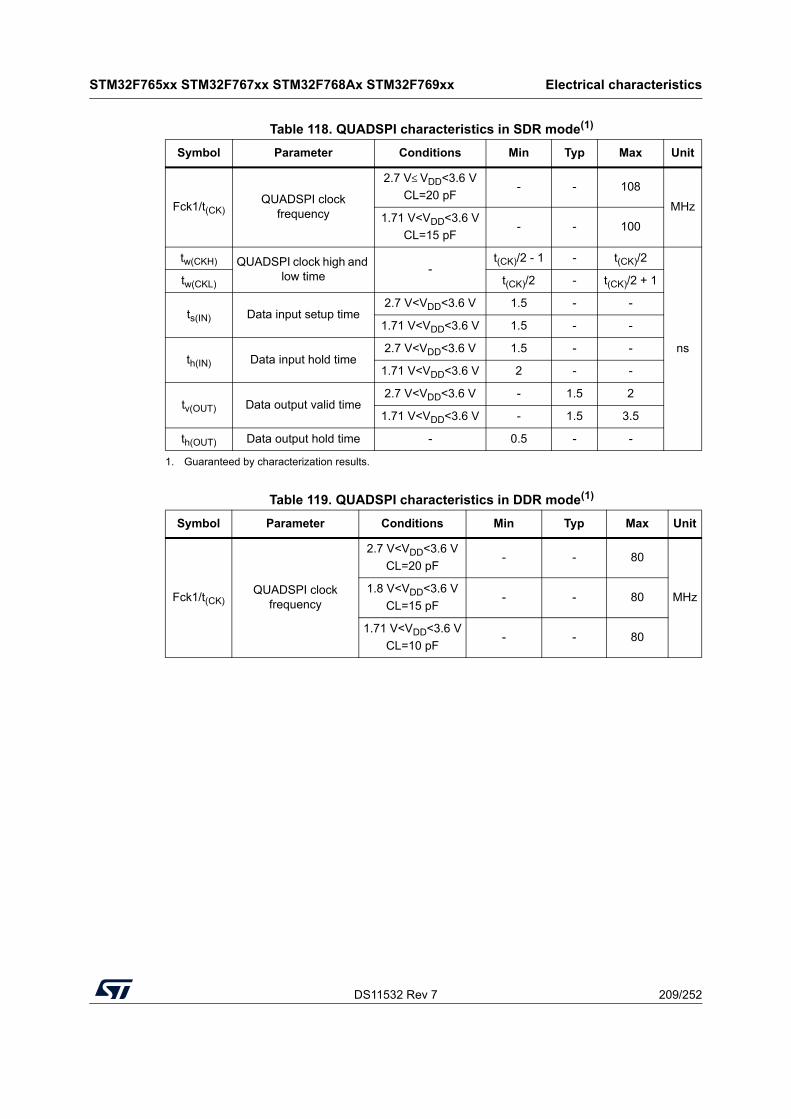
DS11532 Rev 7 209/252
STM32F765xx STM32F767xx STM32F768Ax STM32F769xx Electrical characteristics
218
Table 118. QUADSPI characteristics in SDR mode(1)
1. Guaranteed by characterization results.
Symbol Parameter Conditions Min Typ Max Unit
Fck1/t(CK)QUADSPI clock
frequency
2.7 V≤ VDD<3.6 V
CL=20 pF- - 108
MHz1.71 V<VDD<3.6 V
CL=15 pF- - 100
tw(CKH) QUADSPI clock high and low time
-t(CK)/2 - 1 - t(CK)/2
ns
tw(CKL) t(CK)/2 - t(CK)/2 + 1
ts(IN) Data input setup time2.7 V<VDD<3.6 V 1.5 - -
1.71 V<VDD<3.6 V 1.5 - -
th(IN) Data input hold time2.7 V<VDD<3.6 V 1.5 - -
1.71 V<VDD<3.6 V 2 - -
tv(OUT) Data output valid time2.7 V<VDD<3.6 V - 1.5 2
1.71 V<VDD<3.6 V - 1.5 3.5
th(OUT) Data output hold time - 0.5 - -
Table 119. QUADSPI characteristics in DDR mode(1)
Symbol Parameter Conditions Min Typ Max Unit
Fck1/t(CK)QUADSPI clock
frequency
2.7 V<VDD<3.6 V
CL=20 pF- - 80
MHz1.8 V<VDD<3.6 V
CL=15 pF- - 80
1.71 V<VDD<3.6 V
CL=10 pF- - 80
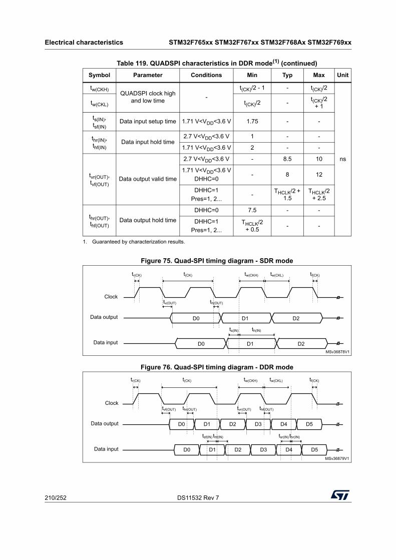
Electrical characteristics STM32F765xx STM32F767xx STM32F768Ax STM32F769xx
210/252 DS11532 Rev 7
Figure 75. Quad-SPI timing diagram - SDR mode
Figure 76. Quad-SPI timing diagram - DDR mode
tw(CKH)QUADSPI clock high
and low time-
t(CK)/2 - 1 - t(CK)/2
ns
tw(CKL) t(CK)/2 -t(CK)/2
+ 1
ts(IN),tsf(IN)
Data input setup time 1.71 V<VDD<3.6 V 1.75 - -
thr(IN), thf(IN)
Data input hold time2.7 V<VDD<3.6 V 1 - -
1.71 V<VDD<3.6 V 2 - -
tvr(OUT), tvf(OUT)
Data output valid time
2.7 V<VDD<3.6 V - 8.5 10
1.71 V<VDD<3.6 V
DHHC=0- 8 12
DHHC=1
Pres=1, 2...-
THCLK/2 + 1.5
THCLK/2 + 2.5
thr(OUT), thf(OUT)
Data output hold time
DHHC=0 7.5 - -
DHHC=1
Pres=1, 2...THCLK/2
+ 0.5- -
1. Guaranteed by characterization results.
Table 119. QUADSPI characteristics in DDR mode(1) (continued)
Symbol Parameter Conditions Min Typ Max Unit
MSv36878V1
Data output D0 D1 D2
Clock
Data input D0 D1 D2
t(CK) tw(CKH) tw(CKL)tr(CK) tf(CK)
ts(IN) th(IN)
tv(OUT) th(OUT)
MSv36879V1
Data output D0 D2 D4
Clock
Data input D0 D2 D4
t(CK) tw(CKH) tw(CKL)tr(CK) tf(CK)
tsf(IN) thf(IN)
tvf(OUT) thr(OUT)
D1 D3 D5
D1 D3 D5
tvr(OUT) thf(OUT)
tsr(IN) thr(IN)
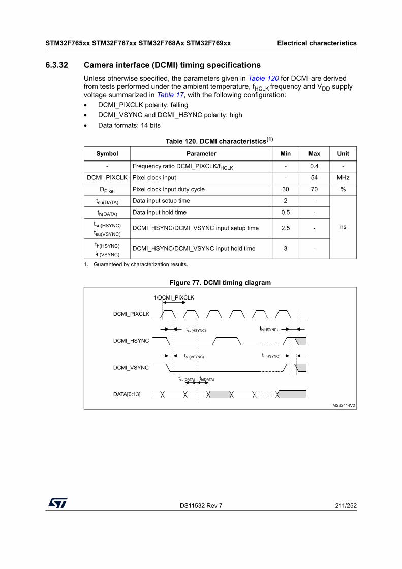
DS11532 Rev 7 211/252
STM32F765xx STM32F767xx STM32F768Ax STM32F769xx Electrical characteristics
218
6.3.32 Camera interface (DCMI) timing specifications
Unless otherwise specified, the parameters given in Table 120 for DCMI are derived from tests performed under the ambient temperature, fHCLK frequency and VDD supply voltage summarized in Table 17, with the following configuration:
• DCMI_PIXCLK polarity: falling
• DCMI_VSYNC and DCMI_HSYNC polarity: high
• Data formats: 14 bits
Figure 77. DCMI timing diagram
Table 120. DCMI characteristics(1)
1. Guaranteed by characterization results.
Symbol Parameter Min Max Unit
- Frequency ratio DCMI_PIXCLK/fHCLK - 0.4 -
DCMI_PIXCLK Pixel clock input - 54 MHz
DPixel Pixel clock input duty cycle 30 70 %
tsu(DATA) Data input setup time 2 -
ns
th(DATA) Data input hold time 0.5 -
tsu(HSYNC)
tsu(VSYNC)DCMI_HSYNC/DCMI_VSYNC input setup time 2.5 -
th(HSYNC)
th(VSYNC)DCMI_HSYNC/DCMI_VSYNC input hold time 3 -
MS32414V2
DCMI_PIXCLK
tsu(VSYNC)
tsu(HSYNC)
DCMI_HSYNC
DCMI_VSYNC
DATA[0:13]
1/DCMI_PIXCLK
th(HSYNC)
th(HSYNC)
tsu(DATA) th(DATA)
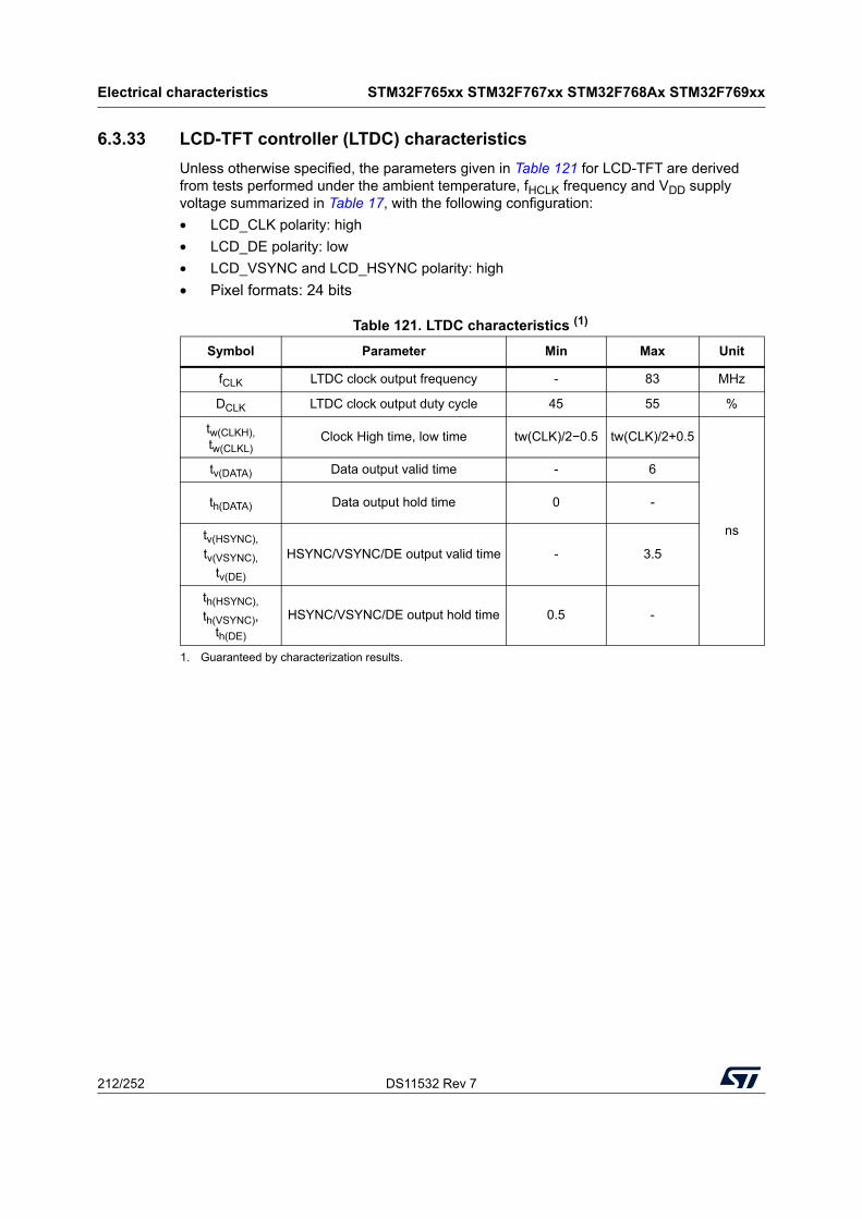
Electrical characteristics STM32F765xx STM32F767xx STM32F768Ax STM32F769xx
212/252 DS11532 Rev 7
6.3.33 LCD-TFT controller (LTDC) characteristics
Unless otherwise specified, the parameters given in Table 121 for LCD-TFT are derived from tests performed under the ambient temperature, fHCLK frequency and VDD supply voltage summarized in Table 17, with the following configuration:
• LCD_CLK polarity: high
• LCD_DE polarity: low
• LCD_VSYNC and LCD_HSYNC polarity: high
• Pixel formats: 24 bits
Table 121. LTDC characteristics (1)
1. Guaranteed by characterization results.
Symbol Parameter Min Max Unit
fCLK LTDC clock output frequency - 83 MHz
DCLK LTDC clock output duty cycle 45 55 %
tw(CLKH),tw(CLKL)
Clock High time, low time tw(CLK)/2−0.5 tw(CLK)/2+0.5
ns
tv(DATA) Data output valid time - 6
th(DATA) Data output hold time 0 -
tv(HSYNC),
tv(VSYNC),
tv(DE)
HSYNC/VSYNC/DE output valid time - 3.5
th(HSYNC),
th(VSYNC),th(DE)
HSYNC/VSYNC/DE output hold time 0.5 -
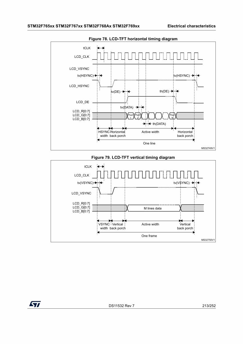
DS11532 Rev 7 213/252
STM32F765xx STM32F767xx STM32F768Ax STM32F769xx Electrical characteristics
218
Figure 78. LCD-TFT horizontal timing diagram
Figure 79. LCD-TFT vertical timing diagram
MS32749V1
LCD_CLK
tv(HSYNC)
LCD_HSYNC
LCD_DE
LCD_R[0:7]LCD_G[0:7]LCD_B[0:7]
tCLK
LCD_VSYNC
tv(HSYNC)
tv(DE) th(DE)
Pixel1
Pixel2
tv(DATA)
th(DATA)
PixelN
HSYNCwidth
Horizontalback porch
Active width Horizontalback porch
One line
MS32750V1
LCD_CLK
tv(VSYNC)
LCD_R[0:7]LCD_G[0:7]LCD_B[0:7]
tCLK
LCD_VSYNC
tv(VSYNC)
M lines data
VSYNCwidth
Verticalback porch
Active width Verticalback porch
One frame
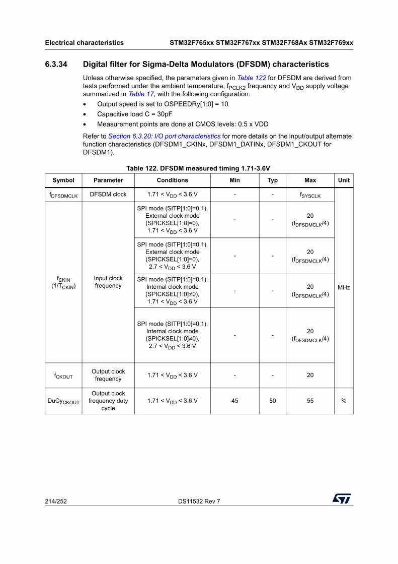
Electrical characteristics STM32F765xx STM32F767xx STM32F768Ax STM32F769xx
214/252 DS11532 Rev 7
6.3.34 Digital filter for Sigma-Delta Modulators (DFSDM) characteristics
Unless otherwise specified, the parameters given in Table 122 for DFSDM are derived from tests performed under the ambient temperature, fPCLK2 frequency and VDD supply voltage summarized in Table 17, with the following configuration:
• Output speed is set to OSPEEDRy[1:0] = 10
• Capacitive load C = 30pF
• Measurement points are done at CMOS levels: 0.5 x VDD
Refer to Section 6.3.20: I/O port characteristics for more details on the input/output alternate function characteristics (DFSDM1_CKINx, DFSDM1_DATINx, DFSDM1_CKOUT for DFSDM1).
Table 122. DFSDM measured timing 1.71-3.6V
Symbol Parameter Conditions Min Typ Max Unit
fDFSDMCLK DFSDM clock 1.71 < VDD < 3.6 V - - fSYSCLK
MHz
fCKIN(1/TCKIN)
Input clock frequency
SPI mode (SITP[1:0]=0,1),External clock mode (SPICKSEL[1:0]=0),1.71 < VDD < 3.6 V
- -20
(fDFSDMCLK/4)
SPI mode (SITP[1:0]=0,1),External clock mode (SPICKSEL[1:0]=0),2.7 < VDD < 3.6 V
- -20
(fDFSDMCLK/4)
SPI mode (SITP[1:0]=0,1),Internal clock mode (SPICKSEL[1:0]≠0),1.71 < VDD < 3.6 V
- -20
(fDFSDMCLK/4)
SPI mode (SITP[1:0]=0,1),Internal clock mode (SPICKSEL[1:0]≠0),
2.7 < VDD < 3.6 V
- -20
(fDFSDMCLK/4)
fCKOUTOutput clock
frequency1.71 < VDD < 3.6 V - - 20
DuCyCKOUT
Output clock frequency duty
cycle1.71 < VDD < 3.6 V 45 50 55 %
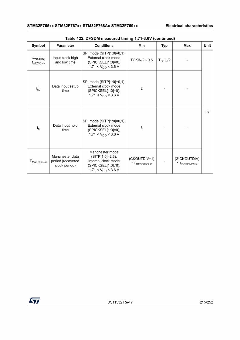
DS11532 Rev 7 215/252
STM32F765xx STM32F767xx STM32F768Ax STM32F769xx Electrical characteristics
218
twh(CKIN)twl(CKIN)
Input clock high and low time
SPI mode (SITP[1:0]=0,1),External clock mode (SPICKSEL[1:0]=0),1.71 < VDD < 3.6 V
TCKIN/2 - 0.5 TCKIN/2 -
ns
tsuData input setup
time
SPI mode (SITP[1:0]=0,1),External clock mode (SPICKSEL[1:0]=0),1.71 < VDD < 3.6 V
2 - -
thData input hold
time
SPI mode (SITP[1:0]=0,1),External clock mode (SPICKSEL[1:0]=0),1.71 < VDD < 3.6 V
3 - -
TManchester
Manchester data period (recovered
clock period)
Manchester mode (SITP[1:0]=2,3),
Internal clock mode (SPICKSEL[1:0]≠0),1.71 < VDD < 3.6 V
(CKOUTDIV+1) * TDFSDMCLK
-(2*CKOUTDIV)
* TDFSDMCLK
Table 122. DFSDM measured timing 1.71-3.6V (continued)
Symbol Parameter Conditions Min Typ Max Unit
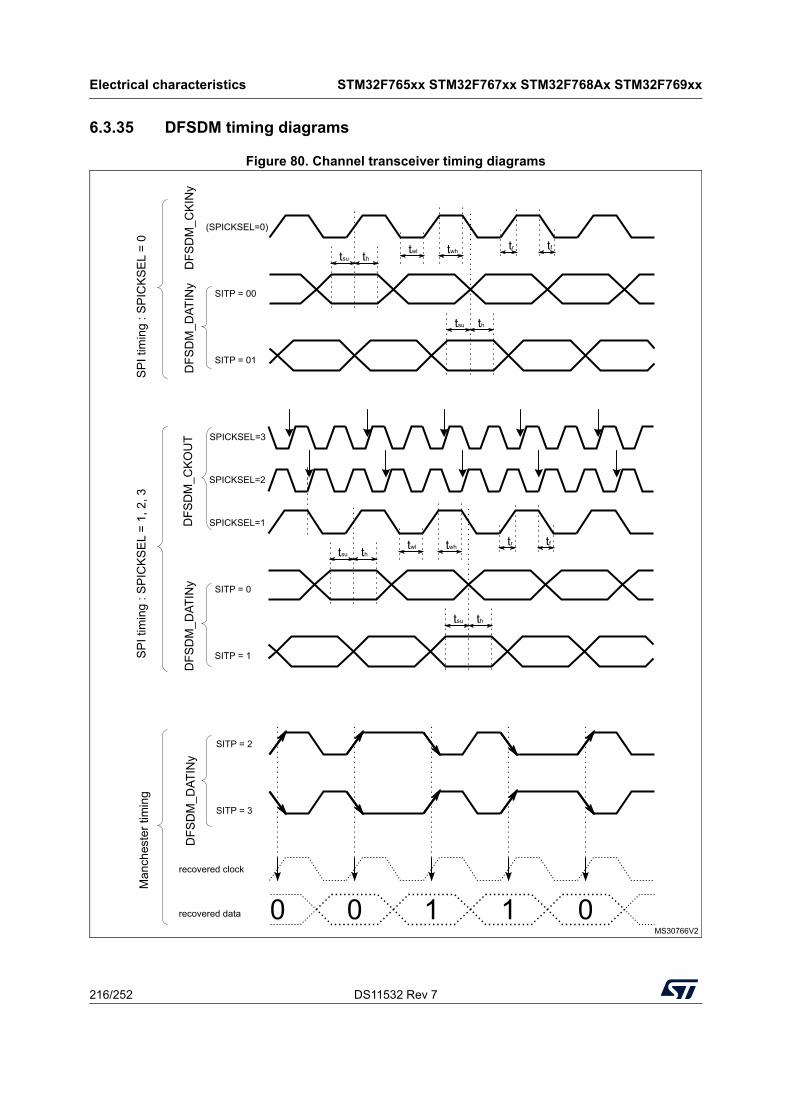
Electrical characteristics STM32F765xx STM32F767xx STM32F768Ax STM32F769xx
216/252 DS11532 Rev 7
6.3.35 DFSDM timing diagrams
Figure 80. Channel transceiver timing diagrams
MS30766V2
SITP = 0
DFS
DM
_CK
OU
TD
FSD
M_D
ATIN
y
SITP = 1
tsu th
tsu th
tftrtwl twh
SP
I tim
ing
: SP
ICK
SE
L =
1, 2
, 3
recovered clock
SITP = 2
DFS
DM
_DAT
INy
SITP = 3
Man
ches
ter t
imin
g
recovered data 1 1 000
SITP = 00
DFS
DM
_CK
INy
DFS
DM
_DAT
INy
SITP = 01
tsu th
tsu th
tftrtwl twh
SP
I tim
ing
: SP
ICK
SE
L =
0
SPICKSEL=2
SPICKSEL=1
(SPICKSEL=0)
SPICKSEL=3
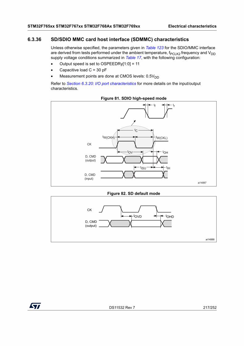
DS11532 Rev 7 217/252
STM32F765xx STM32F767xx STM32F768Ax STM32F769xx Electrical characteristics
218
6.3.36 SD/SDIO MMC card host interface (SDMMC) characteristics
Unless otherwise specified, the parameters given in Table 123 for the SDIO/MMC interface are derived from tests performed under the ambient temperature, fPCLK2 frequency and VDD supply voltage conditions summarized in Table 17, with the following configuration:
• Output speed is set to OSPEEDRy[1:0] = 11
• Capacitive load C = 30 pF
• Measurement points are done at CMOS levels: 0.5VDD
Refer to Section 6.3.20: I/O port characteristics for more details on the input/output characteristics.
Figure 81. SDIO high-speed mode
Figure 82. SD default mode
ai14888
CK
D, CMD(output)
tOVD tOHD
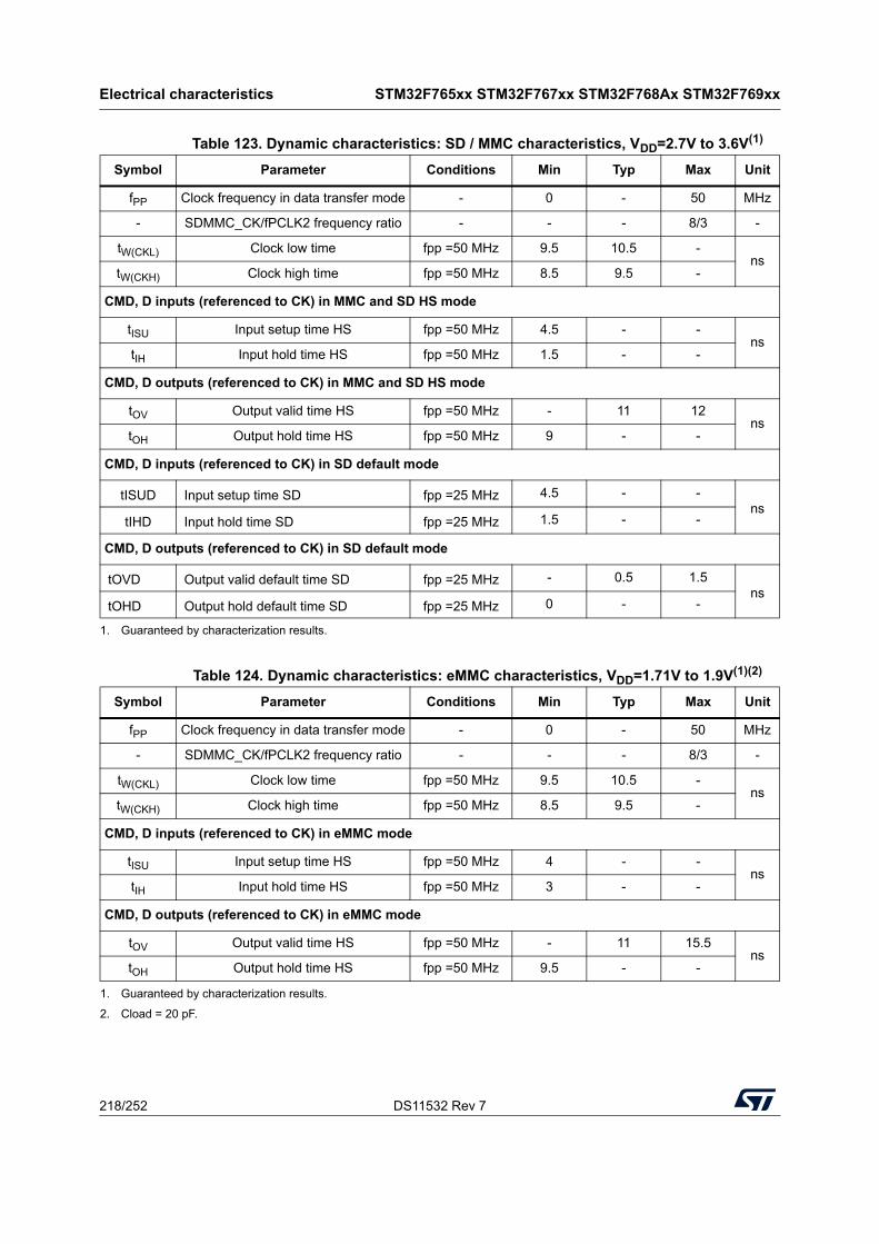
Electrical characteristics STM32F765xx STM32F767xx STM32F768Ax STM32F769xx
218/252 DS11532 Rev 7
Table 123. Dynamic characteristics: SD / MMC characteristics, VDD=2.7V to 3.6V(1)
Symbol Parameter Conditions Min Typ Max Unit
fPP Clock frequency in data transfer mode - 0 - 50 MHz
- SDMMC_CK/fPCLK2 frequency ratio - - - 8/3 -
tW(CKL) Clock low time fpp =50 MHz 9.5 10.5 -ns
tW(CKH) Clock high time fpp =50 MHz 8.5 9.5 -
CMD, D inputs (referenced to CK) in MMC and SD HS mode
tISU Input setup time HS fpp =50 MHz 4.5 - -ns
tIH Input hold time HS fpp =50 MHz 1.5 - -
CMD, D outputs (referenced to CK) in MMC and SD HS mode
tOV Output valid time HS fpp =50 MHz - 11 12ns
tOH Output hold time HS fpp =50 MHz 9 - -
CMD, D inputs (referenced to CK) in SD default mode
tISUD Input setup time SD fpp =25 MHz 4.5 - -ns
tIHD Input hold time SD fpp =25 MHz 1.5 - -
CMD, D outputs (referenced to CK) in SD default mode
tOVD Output valid default time SD fpp =25 MHz - 0.5 1.5ns
tOHD Output hold default time SD fpp =25 MHz 0 - -
1. Guaranteed by characterization results.
Table 124. Dynamic characteristics: eMMC characteristics, VDD=1.71V to 1.9V(1)(2)
Symbol Parameter Conditions Min Typ Max Unit
fPP Clock frequency in data transfer mode - 0 - 50 MHz
- SDMMC_CK/fPCLK2 frequency ratio - - - 8/3 -
tW(CKL) Clock low time fpp =50 MHz 9.5 10.5 -ns
tW(CKH) Clock high time fpp =50 MHz 8.5 9.5 -
CMD, D inputs (referenced to CK) in eMMC mode
tISU Input setup time HS fpp =50 MHz 4 - -ns
tIH Input hold time HS fpp =50 MHz 3 - -
CMD, D outputs (referenced to CK) in eMMC mode
tOV Output valid time HS fpp =50 MHz - 11 15.5ns
tOH Output hold time HS fpp =50 MHz 9.5 - -
1. Guaranteed by characterization results.
2. Cload = 20 pF.
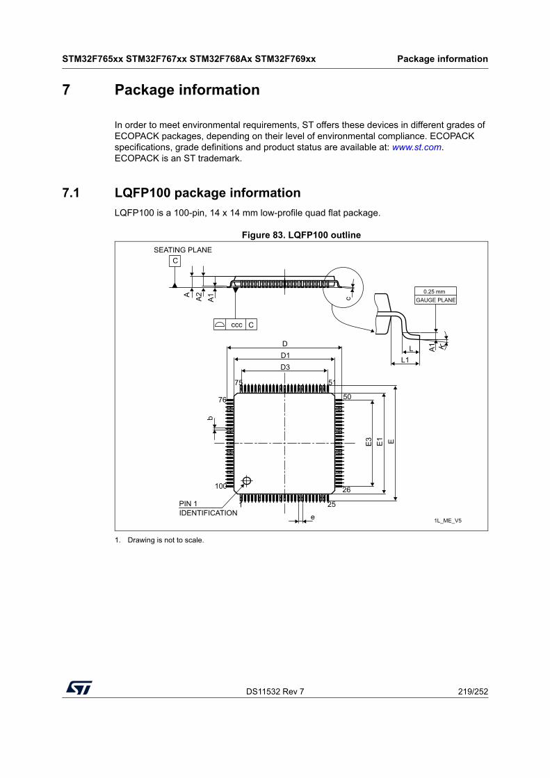
DS11532 Rev 7 219/252
STM32F765xx STM32F767xx STM32F768Ax STM32F769xx Package information
251
7 Package information
In order to meet environmental requirements, ST offers these devices in different grades of ECOPACK packages, depending on their level of environmental compliance. ECOPACK specifications, grade definitions and product status are available at: www.st.com. ECOPACK is an ST trademark.
7.1 LQFP100 package information
LQFP100 is a 100-pin, 14 x 14 mm low-profile quad flat package.
Figure 83. LQFP100 outline
1. Drawing is not to scale.
eIDENTIFICATIONPIN 1
GAUGE PLANE0.25 mm
SEATING PLANE
DD1D3
E3 E1 E
K
ccc C
C
1 25
26100
76
75 51
50
1L_ME_V5
A2A A1
L1L
c
b
A1
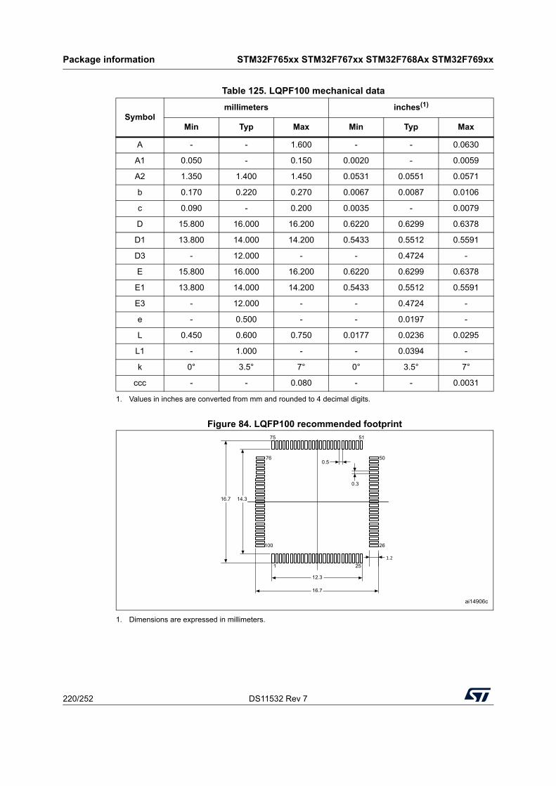
Package information STM32F765xx STM32F767xx STM32F768Ax STM32F769xx
220/252 DS11532 Rev 7
Figure 84. LQFP100 recommended footprint
1. Dimensions are expressed in millimeters.
Table 125. LQPF100 mechanical data
Symbolmillimeters inches(1)
1. Values in inches are converted from mm and rounded to 4 decimal digits.
Min Typ Max Min Typ Max
A - - 1.600 - - 0.0630
A1 0.050 - 0.150 0.0020 - 0.0059
A2 1.350 1.400 1.450 0.0531 0.0551 0.0571
b 0.170 0.220 0.270 0.0067 0.0087 0.0106
c 0.090 - 0.200 0.0035 - 0.0079
D 15.800 16.000 16.200 0.6220 0.6299 0.6378
D1 13.800 14.000 14.200 0.5433 0.5512 0.5591
D3 - 12.000 - - 0.4724 -
E 15.800 16.000 16.200 0.6220 0.6299 0.6378
E1 13.800 14.000 14.200 0.5433 0.5512 0.5591
E3 - 12.000 - - 0.4724 -
e - 0.500 - - 0.0197 -
L 0.450 0.600 0.750 0.0177 0.0236 0.0295
L1 - 1.000 - - 0.0394 -
k 0° 3.5° 7° 0° 3.5° 7°
ccc - - 0.080 - - 0.0031
75 51
50760.5
0.3
16.7 14.3
100 26
12.3
251.2
16.7
1
ai14906c
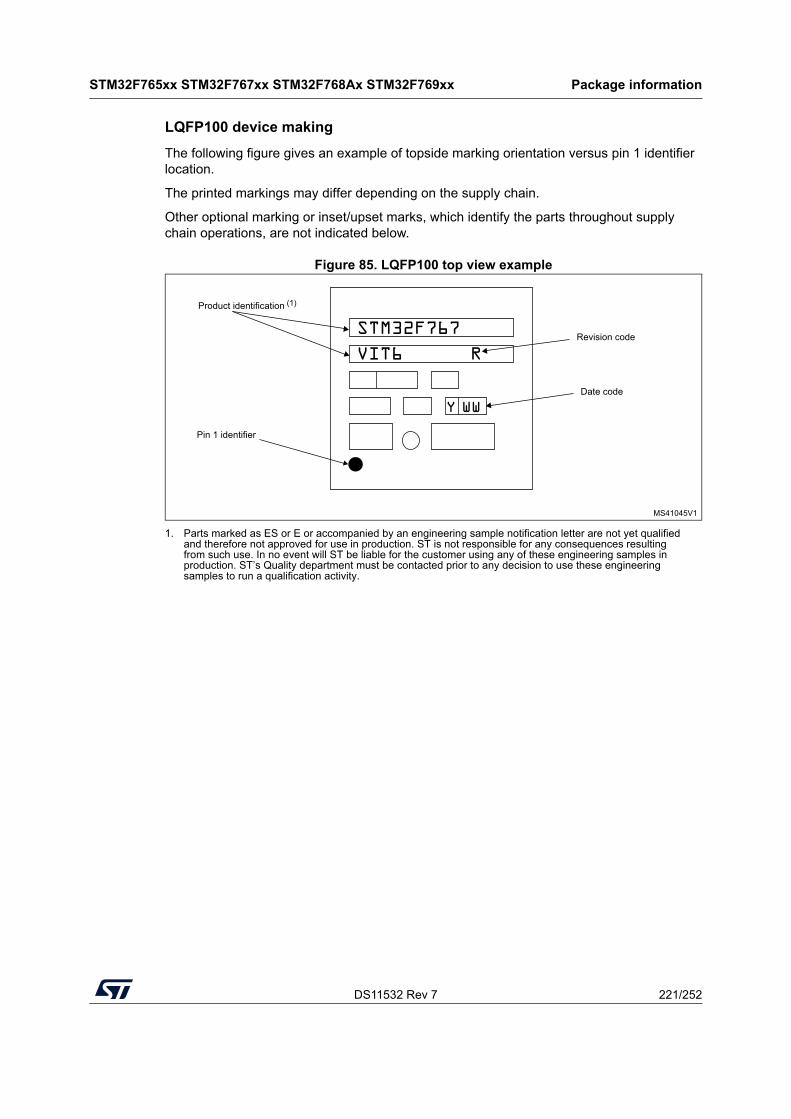
DS11532 Rev 7 221/252
STM32F765xx STM32F767xx STM32F768Ax STM32F769xx Package information
251
LQFP100 device making
The following figure gives an example of topside marking orientation versus pin 1 identifier location.
The printed markings may differ depending on the supply chain.
Other optional marking or inset/upset marks, which identify the parts throughout supply chain operations, are not indicated below.
Figure 85. LQFP100 top view example
1. Parts marked as ES or E or accompanied by an engineering sample notification letter are not yet qualified and therefore not approved for use in production. ST is not responsible for any consequences resulting from such use. In no event will ST be liable for the customer using any of these engineering samples in production. ST’s Quality department must be contacted prior to any decision to use these engineering samples to run a qualification activity.
MS41045V1
STM32F767
VIT6 R
Product identification (1)
Revision code
WWYDate code
Pin 1 identifier
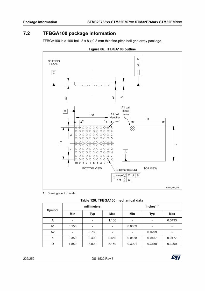
Package information STM32F765xx STM32F767xx STM32F768Ax STM32F769xx
222/252 DS11532 Rev 7
7.2 TFBGA100 package information
TFBGA100 is a 100-ball, 8 x 8 x 0.8 mm thin fine-pitch ball grid array package.
Figure 86. TFBGA100 outline
1. Drawing is not to scale.
Table 126. TFBGA100 mechanical data
Symbolmillimeters inches(1)
Min Typ Max Min Typ Max
A - - 1.100 - - 0.0433
A1 0.150 - - 0.0059 - -
A2 - 0.760 - - 0.0299 -
b 0.350 0.400 0.450 0.0138 0.0157 0.0177
D 7.850 8.000 8.150 0.3091 0.3150 0.3209
SEATINGPLANE
12345678910KJHGFEDCBA
A2 A1 A
C
ddd
C
(100 BALLS)b
eeefff
C A BC
D
E
Fe
B
Ge
A1 ball identifier
A1 ball index area
A
A08Q_ME_V1
D1
E1
BOTTOM VIEW TOP VIEW
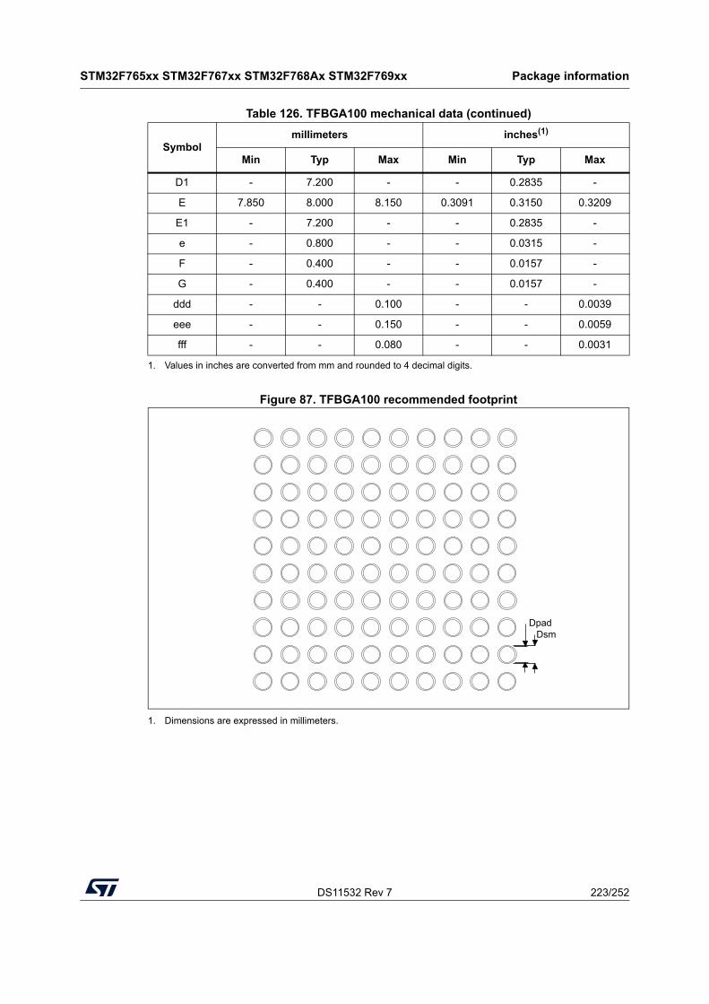
DS11532 Rev 7 223/252
STM32F765xx STM32F767xx STM32F768Ax STM32F769xx Package information
251
Figure 87. TFBGA100 recommended footprint
1. Dimensions are expressed in millimeters.
D1 - 7.200 - - 0.2835 -
E 7.850 8.000 8.150 0.3091 0.3150 0.3209
E1 - 7.200 - - 0.2835 -
e - 0.800 - - 0.0315 -
F - 0.400 - - 0.0157 -
G - 0.400 - - 0.0157 -
ddd - - 0.100 - - 0.0039
eee - - 0.150 - - 0.0059
fff - - 0.080 - - 0.0031
1. Values in inches are converted from mm and rounded to 4 decimal digits.
Table 126. TFBGA100 mechanical data (continued)
Symbolmillimeters inches(1)
Min Typ Max Min Typ Max
DpadDsm
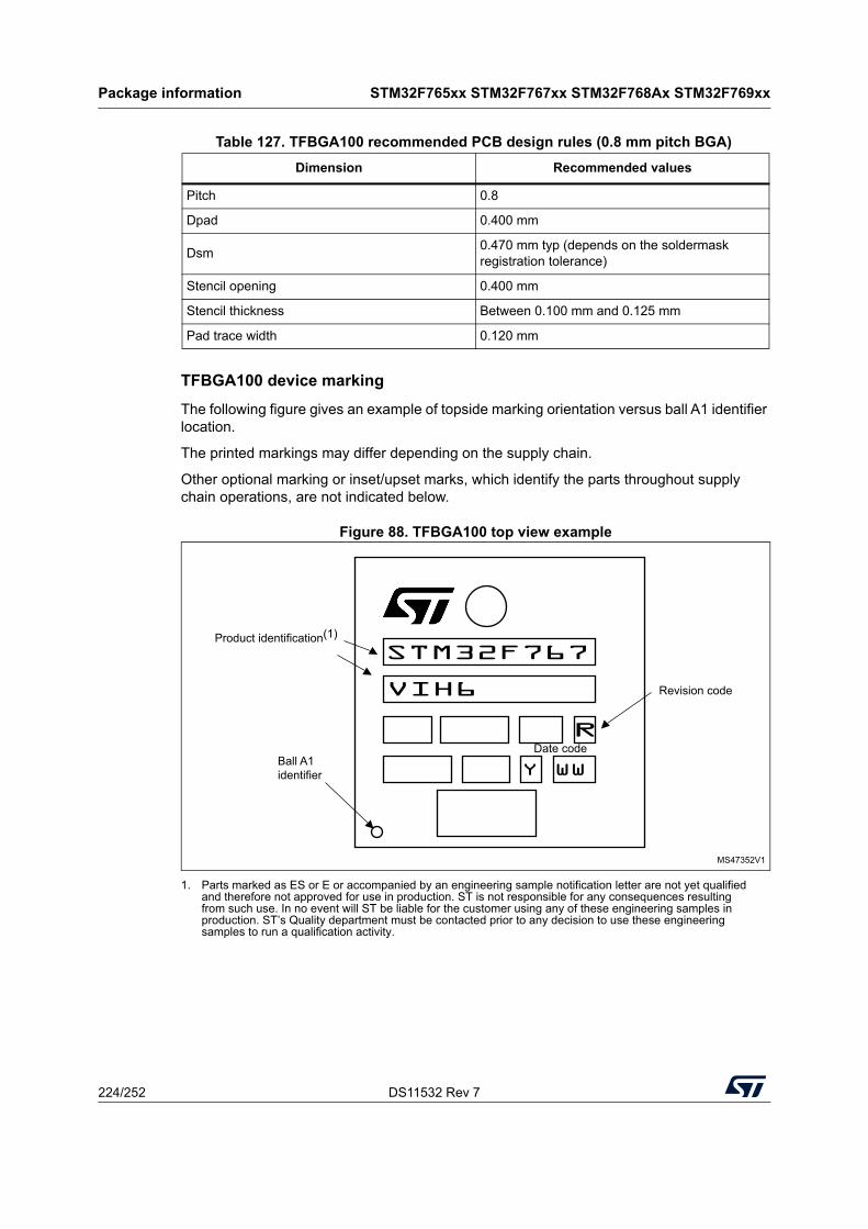
Package information STM32F765xx STM32F767xx STM32F768Ax STM32F769xx
224/252 DS11532 Rev 7
TFBGA100 device marking
The following figure gives an example of topside marking orientation versus ball A1 identifier location.
The printed markings may differ depending on the supply chain.
Other optional marking or inset/upset marks, which identify the parts throughout supply chain operations, are not indicated below.
Figure 88. TFBGA100 top view example
1. Parts marked as ES or E or accompanied by an engineering sample notification letter are not yet qualified and therefore not approved for use in production. ST is not responsible for any consequences resulting from such use. In no event will ST be liable for the customer using any of these engineering samples in production. ST’s Quality department must be contacted prior to any decision to use these engineering samples to run a qualification activity.
Table 127. TFBGA100 recommended PCB design rules (0.8 mm pitch BGA)
Dimension Recommended values
Pitch 0.8
Dpad 0.400 mm
Dsm0.470 mm typ (depends on the soldermask registration tolerance)
Stencil opening 0.400 mm
Stencil thickness Between 0.100 mm and 0.125 mm
Pad trace width 0.120 mm
MS47352V1
Ball A1identifier
Date code
Y WW
Revision code
Product identification(1)
R
STM32F767
VIH6
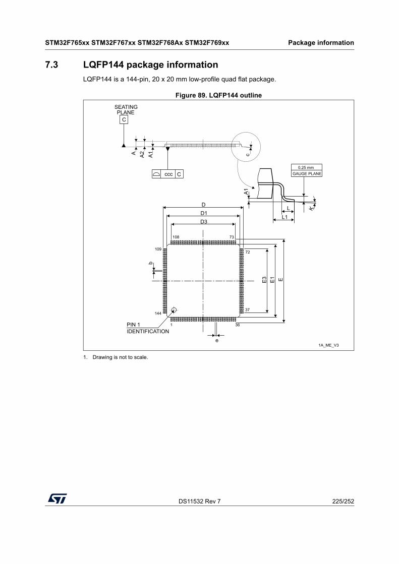
DS11532 Rev 7 225/252
STM32F765xx STM32F767xx STM32F768Ax STM32F769xx Package information
251
7.3 LQFP144 package information
LQFP144 is a 144-pin, 20 x 20 mm low-profile quad flat package.
Figure 89. LQFP144 outline
1. Drawing is not to scale.
eIDENTIFICATIONPIN 1
GAUGE PLANE0.25 mm
SEATINGPLANE
DD1D3
E3 E1 E
K
ccc C
C
1 36
37144
109
108 73
72
1A_ME_V3
A2A A1
L1L
c
b
A1
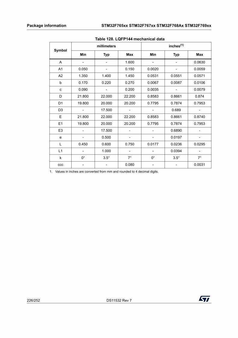
Package information STM32F765xx STM32F767xx STM32F768Ax STM32F769xx
226/252 DS11532 Rev 7
Table 128. LQFP144 mechanical data
Symbolmillimeters inches(1)
1. Values in inches are converted from mm and rounded to 4 decimal digits.
Min Typ Max Min Typ Max
A - - 1.600 - - 0.0630
A1 0.050 - 0.150 0.0020 - 0.0059
A2 1.350 1.400 1.450 0.0531 0.0551 0.0571
b 0.170 0.220 0.270 0.0067 0.0087 0.0106
c 0.090 - 0.200 0.0035 - 0.0079
D 21.800 22.000 22.200 0.8583 0.8661 0.874
D1 19.800 20.000 20.200 0.7795 0.7874 0.7953
D3 - 17.500 - - 0.689 -
E 21.800 22.000 22.200 0.8583 0.8661 0.8740
E1 19.800 20.000 20.200 0.7795 0.7874 0.7953
E3 - 17.500 - - 0.6890 -
e - 0.500 - - 0.0197 -
L 0.450 0.600 0.750 0.0177 0.0236 0.0295
L1 - 1.000 - - 0.0394 -
k 0° 3.5° 7° 0° 3.5° 7°
ccc - - 0.080 - - 0.0031
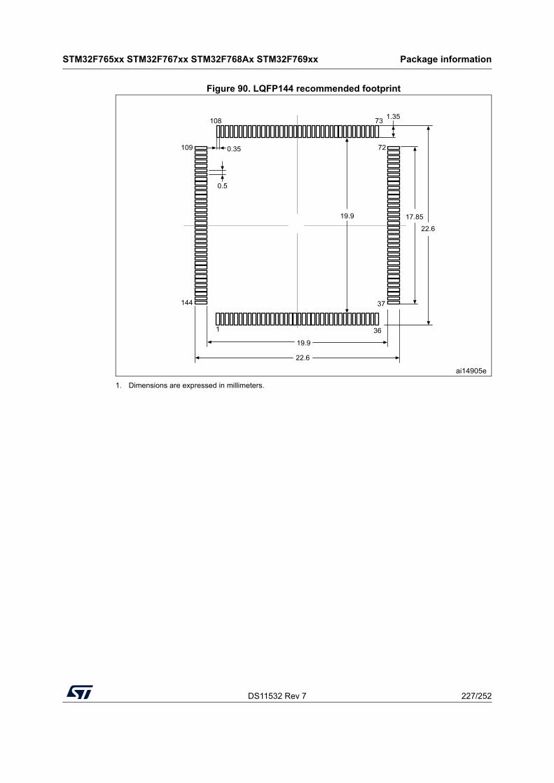
DS11532 Rev 7 227/252
STM32F765xx STM32F767xx STM32F768Ax STM32F769xx Package information
251
Figure 90. LQFP144 recommended footprint
1. Dimensions are expressed in millimeters.
0.5
0.35
19.9 17.85
22.6
1.35
22.6
19.9
ai14905e
1 36
37
72
73108
109
144
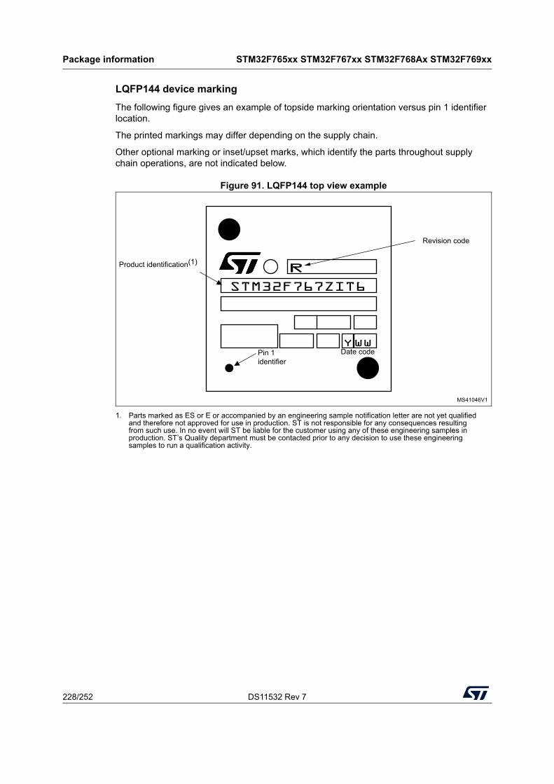
Package information STM32F765xx STM32F767xx STM32F768Ax STM32F769xx
228/252 DS11532 Rev 7
LQFP144 device marking
The following figure gives an example of topside marking orientation versus pin 1 identifier location.
The printed markings may differ depending on the supply chain.
Other optional marking or inset/upset marks, which identify the parts throughout supply chain operations, are not indicated below.
Figure 91. LQFP144 top view example
1. Parts marked as ES or E or accompanied by an engineering sample notification letter are not yet qualified and therefore not approved for use in production. ST is not responsible for any consequences resulting from such use. In no event will ST be liable for the customer using any of these engineering samples in production. ST’s Quality department must be contacted prior to any decision to use these engineering samples to run a qualification activity.
MS41046V1
Pin 1identifier
R
Revision code
Product identification(1)
Date codeYWW
STM32F767ZIT6
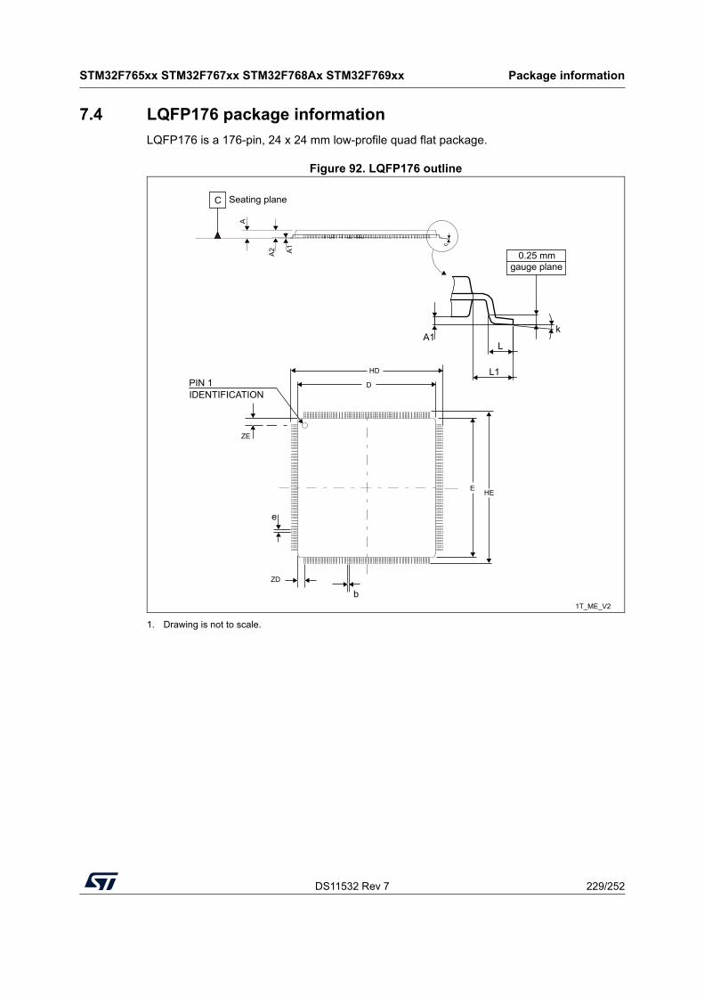
DS11532 Rev 7 229/252
STM32F765xx STM32F767xx STM32F768Ax STM32F769xx Package information
251
7.4 LQFP176 package information
LQFP176 is a 176-pin, 24 x 24 mm low-profile quad flat package.
Figure 92. LQFP176 outline
1. Drawing is not to scale.
1T_ME_V2
A2
A
e
E HE
D
HD
ZD
ZE
b
0.25 mmgauge plane
A1L
L1
k
c
IDENTIFICATIONPIN 1
Seating planeC
A1
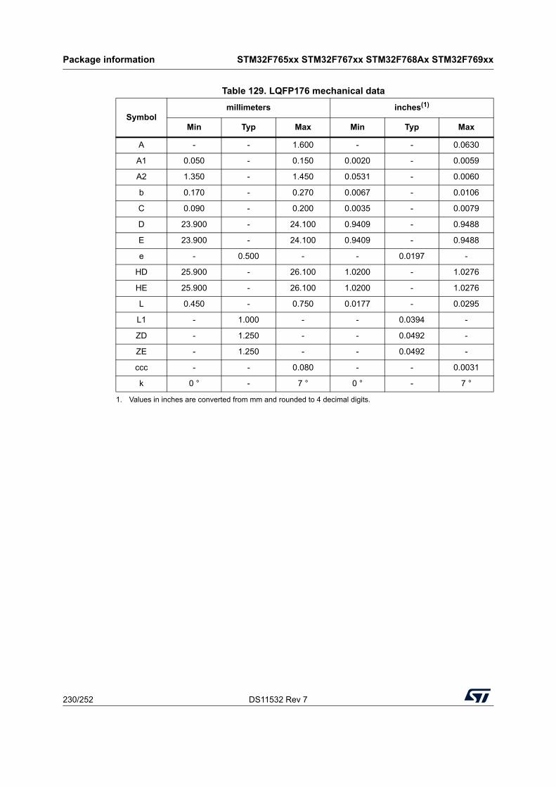
Package information STM32F765xx STM32F767xx STM32F768Ax STM32F769xx
230/252 DS11532 Rev 7
Table 129. LQFP176 mechanical data
Symbolmillimeters inches(1)
1. Values in inches are converted from mm and rounded to 4 decimal digits.
Min Typ Max Min Typ Max
A - - 1.600 - - 0.0630
A1 0.050 - 0.150 0.0020 - 0.0059
A2 1.350 - 1.450 0.0531 - 0.0060
b 0.170 - 0.270 0.0067 - 0.0106
C 0.090 - 0.200 0.0035 - 0.0079
D 23.900 - 24.100 0.9409 - 0.9488
E 23.900 - 24.100 0.9409 - 0.9488
e - 0.500 - - 0.0197 -
HD 25.900 - 26.100 1.0200 - 1.0276
HE 25.900 - 26.100 1.0200 - 1.0276
L 0.450 - 0.750 0.0177 - 0.0295
L1 - 1.000 - - 0.0394 -
ZD - 1.250 - - 0.0492 -
ZE - 1.250 - - 0.0492 -
ccc - - 0.080 - - 0.0031
k 0 ° - 7 ° 0 ° - 7 °
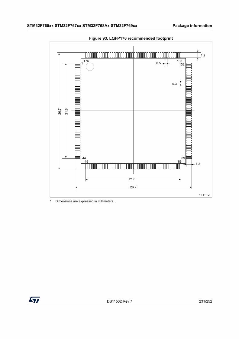
DS11532 Rev 7 231/252
STM32F765xx STM32F767xx STM32F768Ax STM32F769xx Package information
251
Figure 93. LQFP176 recommended footprint
1. Dimensions are expressed in millimeters.
1T_FP_V1
133132
1.2
0.3
0.5
8988
1.2
4445
21.8
26.7
1176
26.7
21.8
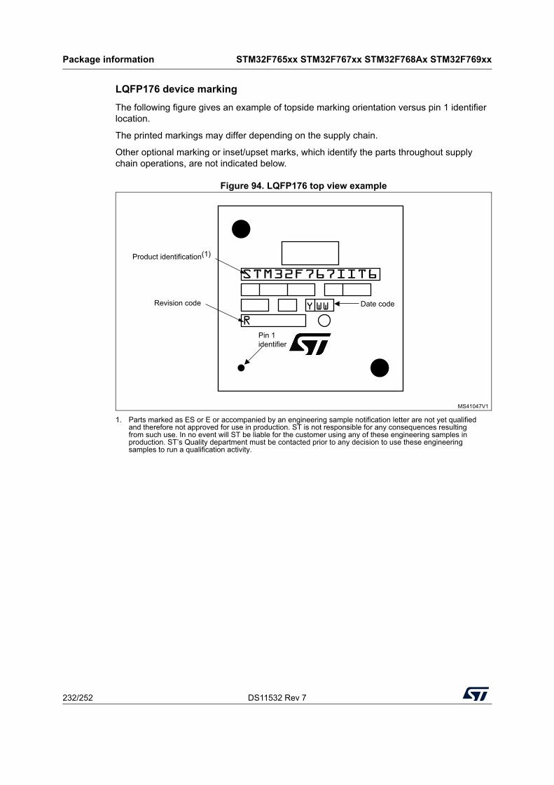
Package information STM32F765xx STM32F767xx STM32F768Ax STM32F769xx
232/252 DS11532 Rev 7
LQFP176 device marking
The following figure gives an example of topside marking orientation versus pin 1 identifier location.
The printed markings may differ depending on the supply chain.
Other optional marking or inset/upset marks, which identify the parts throughout supply chain operations, are not indicated below.
Figure 94. LQFP176 top view example
1. Parts marked as ES or E or accompanied by an engineering sample notification letter are not yet qualified and therefore not approved for use in production. ST is not responsible for any consequences resulting from such use. In no event will ST be liable for the customer using any of these engineering samples in production. ST’s Quality department must be contacted prior to any decision to use these engineering samples to run a qualification activity.
MS41047V1
WWY
Pin 1identifier
STM32F767IIT6
R
Date code
Product identification(1)
Revision code
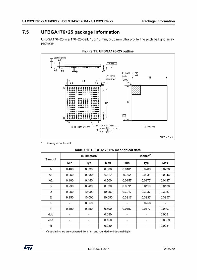
DS11532 Rev 7 233/252
STM32F765xx STM32F767xx STM32F768Ax STM32F769xx Package information
251
7.5 UFBGA176+25 package information
UFBGA176+25 is a 176+25-ball, 10 x 10 mm, 0.65 mm ultra profile fine pitch ball grid array package.
Figure 95. UFBGA176+25 outline
1. Drawing is not to scale.
Table 130. UFBGA176+25 mechanical data
Symbolmillimeters inches(1)
1. Values in inches are converted from mm and rounded to 4 decimal digits.
Min Typ Max Min Typ Max
A 0.460 0.530 0.600 0.0181 0.0209 0.0236
A1 0.050 0.080 0.110 0.002 0.0031 0.0043
A2 0.400 0.450 0.500 0.0157 0.0177 0.0197
b 0.230 0.280 0.330 0.0091 0.0110 0.0130
D 9.950 10.000 10.050 0.3917 0.3937 0.3957
E 9.950 10.000 10.050 0.3917 0.3937 0.3957
e - 0.650 - - 0.0256 -
F 0.400 0.450 0.500 0.0157 0.0177 0.0197
ddd - - 0.080 - - 0.0031
eee - - 0.150 - - 0.0059
fff - - 0.080 - - 0.0031
A0E7_ME_V10
Seating plane
A2
Cddd
A1A
e F
F
e
R
A
15 1
BOTTOM VIEW
E
D
TOP VIEWØb (176 + 25 balls)
B
A
BeeeØ MfffØ M
CC
A
C
A1 ball identifier
A1 ball index area
b
A4
E1
A3
D1
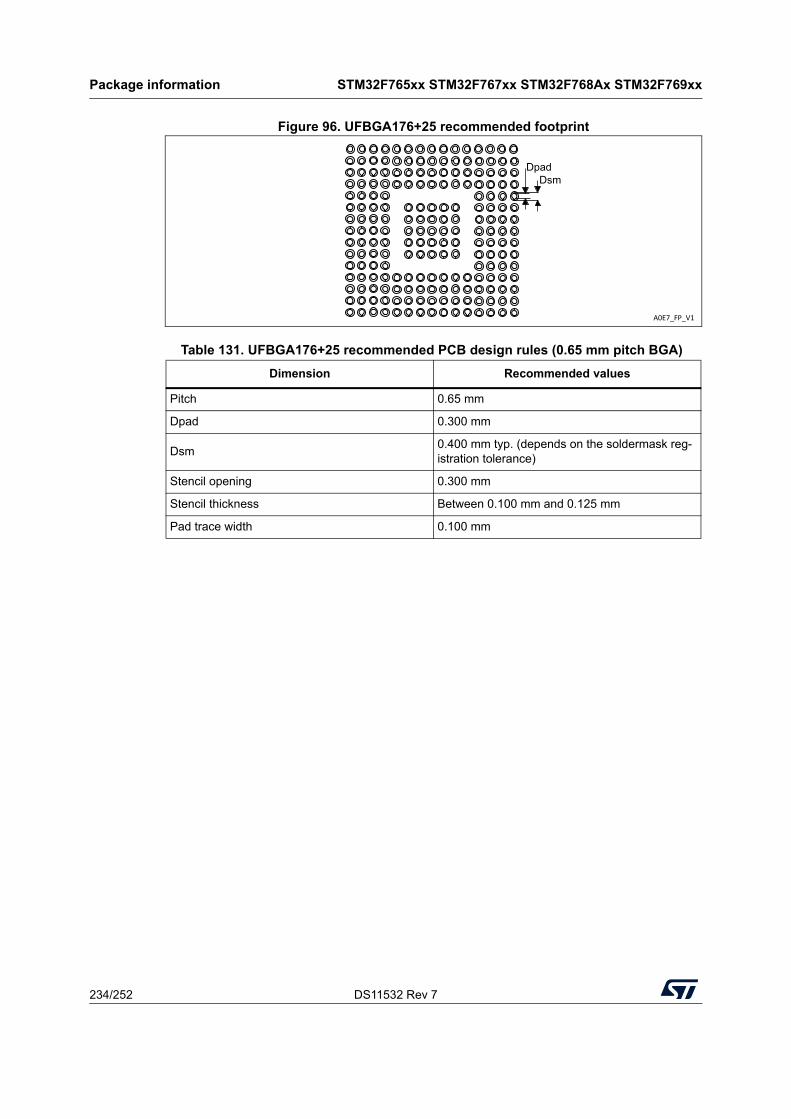
Package information STM32F765xx STM32F767xx STM32F768Ax STM32F769xx
234/252 DS11532 Rev 7
Figure 96. UFBGA176+25 recommended footprint
Table 131. UFBGA176+25 recommended PCB design rules (0.65 mm pitch BGA)
Dimension Recommended values
Pitch 0.65 mm
Dpad 0.300 mm
Dsm0.400 mm typ. (depends on the soldermask reg-istration tolerance)
Stencil opening 0.300 mm
Stencil thickness Between 0.100 mm and 0.125 mm
Pad trace width 0.100 mm
A0E7_FP_V1
DpadDsm
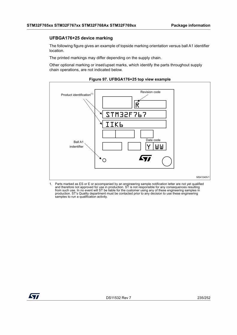
DS11532 Rev 7 235/252
STM32F765xx STM32F767xx STM32F768Ax STM32F769xx Package information
251
UFBGA176+25 device marking
The following figure gives an example of topside marking orientation versus ball A1 identifier location.
The printed markings may differ depending on the supply chain.
Other optional marking or inset/upset marks, which identify the parts throughout supply chain operations, are not indicated below.
Figure 97. UFBGA176+25 top view example
1. Parts marked as ES or E or accompanied by an engineering sample notification letter are not yet qualified and therefore not approved for use in production. ST is not responsible for any consequences resulting from such use. In no event will ST be liable for the customer using any of these engineering samples in production. ST’s Quality department must be contacted prior to any decision to use these engineering samples to run a qualification activity.
MS41049V1
Revision code
STM32F767
Product identification(1)
Date code
Y WWBall A1
indentifier
IIK6
R
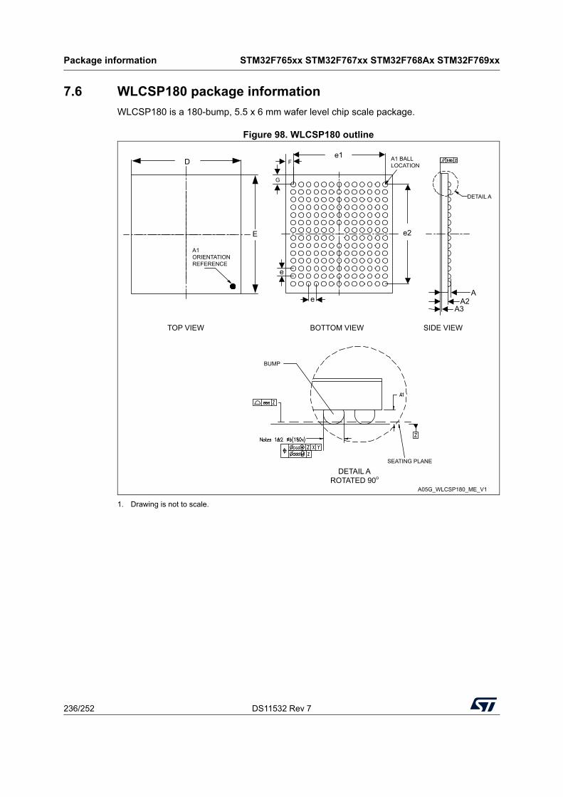
Package information STM32F765xx STM32F767xx STM32F768Ax STM32F769xx
236/252 DS11532 Rev 7
7.6 WLCSP180 package information
WLCSP180 is a 180-bump, 5.5 x 6 mm wafer level chip scale package.
Figure 98. WLCSP180 outline
1. Drawing is not to scale.
TOP VIEW BOTTOM VIEW
D
E
A1ORIENTATIONREFERENCE
G
Fe1 A1 BALL
LOCATION
e
e
e2
A3A2
A
DETAIL A
SIDE VIEW
A05G_WLCSP180_ME_V1
DETAIL AROTATED 90o
BUMP
SEATING PLANE
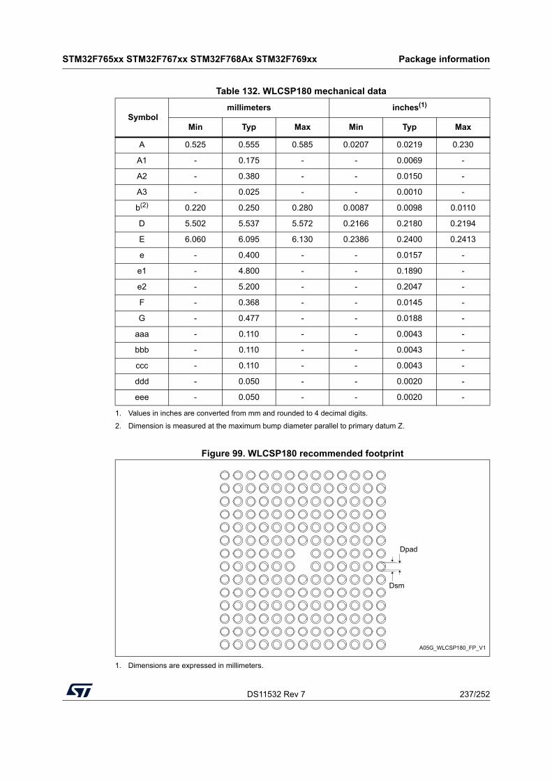
DS11532 Rev 7 237/252
STM32F765xx STM32F767xx STM32F768Ax STM32F769xx Package information
251
Figure 99. WLCSP180 recommended footprint
1. Dimensions are expressed in millimeters.
Table 132. WLCSP180 mechanical data
Symbolmillimeters inches(1)
1. Values in inches are converted from mm and rounded to 4 decimal digits.
Min Typ Max Min Typ Max
A 0.525 0.555 0.585 0.0207 0.0219 0.230
A1 - 0.175 - - 0.0069 -
A2 - 0.380 - - 0.0150 -
A3 - 0.025 - - 0.0010 -
b(2)
2. Dimension is measured at the maximum bump diameter parallel to primary datum Z.
0.220 0.250 0.280 0.0087 0.0098 0.0110
D 5.502 5.537 5.572 0.2166 0.2180 0.2194
E 6.060 6.095 6.130 0.2386 0.2400 0.2413
e - 0.400 - - 0.0157 -
e1 - 4.800 - - 0.1890 -
e2 - 5.200 - - 0.2047 -
F - 0.368 - - 0.0145 -
G - 0.477 - - 0.0188 -
aaa - 0.110 - - 0.0043 -
bbb - 0.110 - - 0.0043 -
ccc - 0.110 - - 0.0043 -
ddd - 0.050 - - 0.0020 -
eee - 0.050 - - 0.0020 -
Dpad
Dsm
A05G_WLCSP180_FP_V1
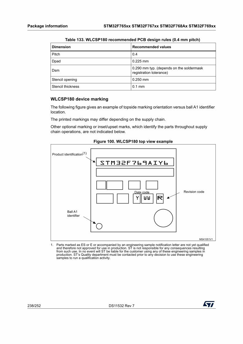
Package information STM32F765xx STM32F767xx STM32F768Ax STM32F769xx
238/252 DS11532 Rev 7
WLCSP180 device marking
The following figure gives an example of topside marking orientation versus ball A1 identifier location.
The printed markings may differ depending on the supply chain.
Other optional marking or inset/upset marks, which identify the parts throughout supply chain operations, are not indicated below.
Figure 100. WLCSP180 top view example
1. Parts marked as ES or E or accompanied by an engineering sample notification letter are not yet qualified and therefore not approved for use in production. ST is not responsible for any consequences resulting from such use. In no event will ST be liable for the customer using any of these engineering samples in production. ST’s Quality department must be contacted prior to any decision to use these engineering samples to run a qualification activity.
Table 133. WLCSP180 recommended PCB design rules (0.4 mm pitch)
Dimension Recommended values
Pitch 0.4
Dpad 0.225 mm
Dsm0.290 mm typ. (depends on the soldermask registration tolerance)
Stencil opening 0.250 mm
Stencil thickness 0.1 mm
MS41051V1
WW
Ball A1identifier
YDate code Revision code
Product identification(1)
R
STM32F769AIY6
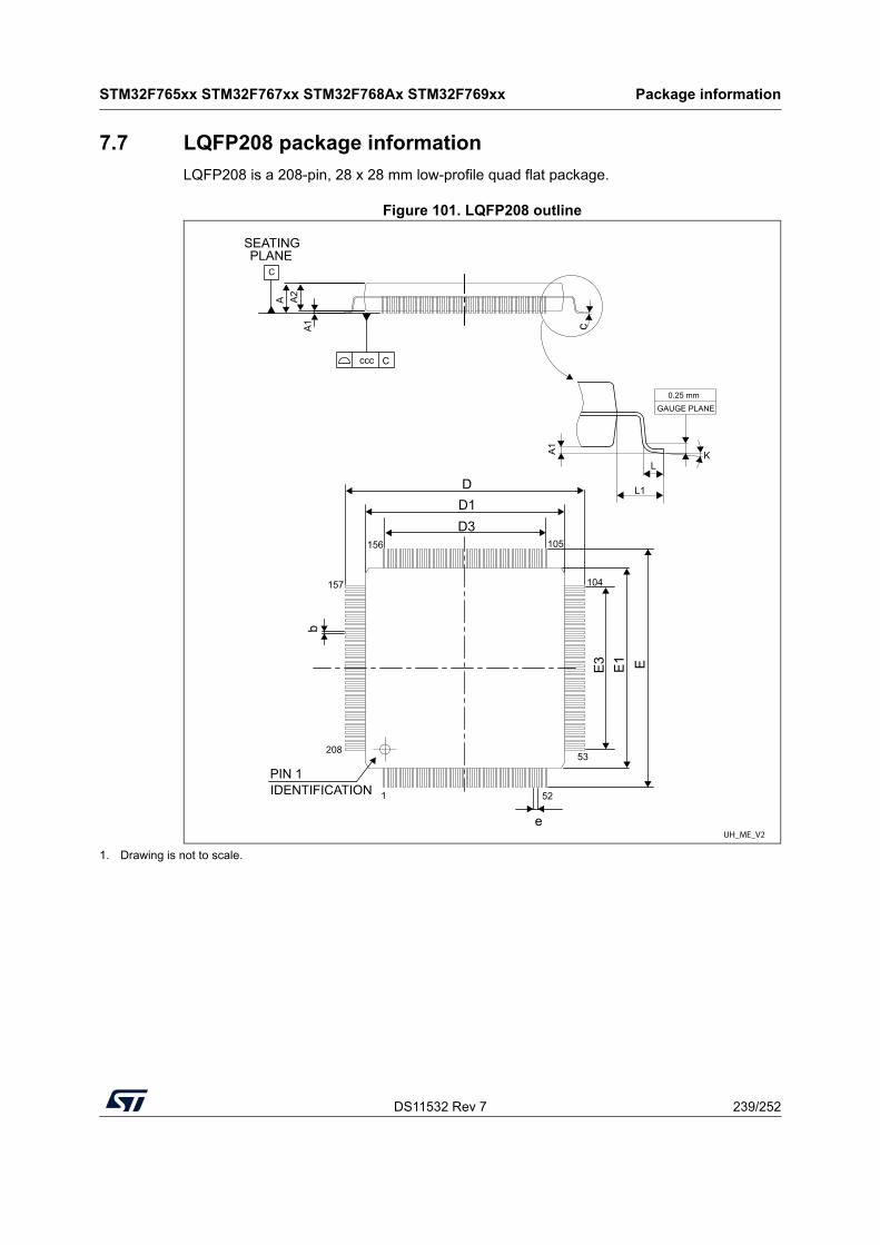
DS11532 Rev 7 239/252
STM32F765xx STM32F767xx STM32F768Ax STM32F769xx Package information
251
7.7 LQFP208 package information
LQFP208 is a 208-pin, 28 x 28 mm low-profile quad flat package.
Figure 101. LQFP208 outline
1. Drawing is not to scale.
DD1D3
E3 E1 E
e
L1
GAUGE PLANE0.25 mm
b
C
SEATINGPLANE
ccc C
IDENTIFICATIONPIN 1
1 52
53
104
105156
157
208
c
L
A1
A1
A A2
UH_ME_V2
K
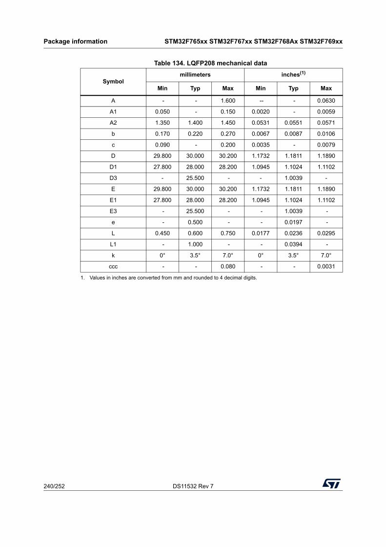
Package information STM32F765xx STM32F767xx STM32F768Ax STM32F769xx
240/252 DS11532 Rev 7
Table 134. LQFP208 mechanical data
Symbolmillimeters inches(1)
1. Values in inches are converted from mm and rounded to 4 decimal digits.
Min Typ Max Min Typ Max
A - - 1.600 -- - 0.0630
A1 0.050 - 0.150 0.0020 - 0.0059
A2 1.350 1.400 1.450 0.0531 0.0551 0.0571
b 0.170 0.220 0.270 0.0067 0.0087 0.0106
c 0.090 - 0.200 0.0035 - 0.0079
D 29.800 30.000 30.200 1.1732 1.1811 1.1890
D1 27.800 28.000 28.200 1.0945 1.1024 1.1102
D3 - 25.500 - - 1.0039 -
E 29.800 30.000 30.200 1.1732 1.1811 1.1890
E1 27.800 28.000 28.200 1.0945 1.1024 1.1102
E3 - 25.500 - - 1.0039 -
e - 0.500 - - 0.0197 -
L 0.450 0.600 0.750 0.0177 0.0236 0.0295
L1 - 1.000 - - 0.0394 -
k 0° 3.5° 7.0° 0° 3.5° 7.0°
ccc - - 0.080 - - 0.0031
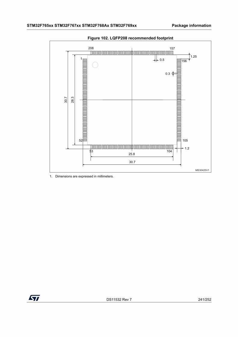
DS11532 Rev 7 241/252
STM32F765xx STM32F767xx STM32F768Ax STM32F769xx Package information
251
Figure 102. LQFP208 recommended footprint
1. Dimensions are expressed in millimeters.
MS30425V1
208 157
0.5
0.3
1
30.7
28.3
52
5325.8
30.7
1.2104
105
1.25156
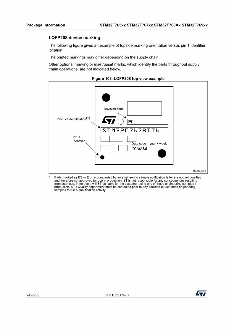
Package information STM32F765xx STM32F767xx STM32F768Ax STM32F769xx
242/252 DS11532 Rev 7
LQFP208 device marking
The following figure gives an example of topside marking orientation versus pin 1 identifier location.
The printed markings may differ depending on the supply chain.
Other optional marking or inset/upset marks, which identify the parts throughout supply chain operations, are not indicated below.
Figure 103. LQFP208 top view example
1. Parts marked as ES or E or accompanied by an engineering sample notification letter are not yet qualified and therefore not approved for use in production. ST is not responsible for any consequences resulting from such use. In no event will ST be liable for the customer using any of these engineering samples in production. ST’s Quality department must be contacted prior to any decision to use these engineering samples to run a qualification activity.
MS41048V1
WWY
Pin 1identifier
Date code = year + week
Revision code
Product identification(1)R
STM32F767BIT6
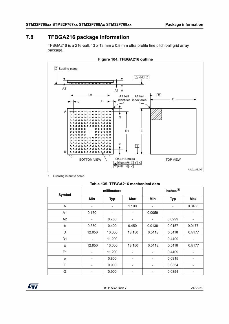
DS11532 Rev 7 243/252
STM32F765xx STM32F767xx STM32F768Ax STM32F769xx Package information
251
7.8 TFBGA216 package information
TFBGA216 is a 216-ball, 13 x 13 mm x 0.8 mm ultra profile fine pitch ball grid array package.
Figure 104. TFBGA216 outline
1. Drawing is not to scale.
Table 135. TFBGA216 mechanical data
Symbolmillimeters inches(1)
Min Typ Max Min Typ Max
A - - 1.100 - - 0.0433
A1 0.150 - - 0.0059 - -
A2 - 0.760 - - 0.0299 -
b 0.350 0.400 0.450 0.0138 0.0157 0.0177
D 12.850 13.000 13.150 0.5118 0.5118 0.5177
D1 - 11.200 - - 0.4409 -
E 12.850 13.000 13.150 0.5118 0.5118 0.5177
E1 - 11.200 - - 0.4409 -
e - 0.800 - - 0.0315 -
F - 0.900 - - 0.0354 -
G - 0.900 - - 0.0354 -
A0L2_ME_V3
Seating plane
A1
e F
G
D
R
Øb (216 balls)
A
E
TOP VIEWBOTTOM VIEW115
e
AA2
Y
X
Z
ddd Z
D1
E1
eee Z Y Xfff
ØØ
MM Z
A1 ball identifier
A1 ball index area
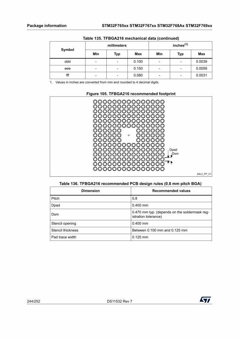
Package information STM32F765xx STM32F767xx STM32F768Ax STM32F769xx
244/252 DS11532 Rev 7
Figure 105. TFBGA216 recommended footprint
ddd - - 0.100 - - 0.0039
eee - - 0.150 - - 0.0059
fff - - 0.080 - - 0.0031
1. Values in inches are converted from mm and rounded to 4 decimal digits.
Table 136. TFBGA216 recommended PCB design rules (0.8 mm pitch BGA)
Dimension Recommended values
Pitch 0.8
Dpad 0.400 mm
Dsm0.470 mm typ. (depends on the soldermask reg-istration tolerance)
Stencil opening 0.400 mm
Stencil thickness Between 0.100 mm and 0.125 mm
Pad trace width 0.120 mm
Table 135. TFBGA216 mechanical data (continued)
Symbolmillimeters inches(1)
Min Typ Max Min Typ Max
A0L2_FP_V1
DpadDsm
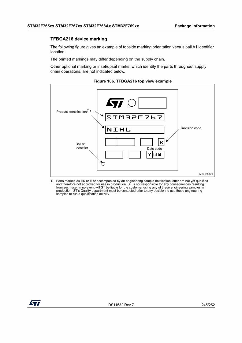
DS11532 Rev 7 245/252
STM32F765xx STM32F767xx STM32F768Ax STM32F769xx Package information
251
TFBGA216 device marking
The following figure gives an example of topside marking orientation versus ball A1 identifier location.
The printed markings may differ depending on the supply chain.
Other optional marking or inset/upset marks, which identify the parts throughout supply chain operations, are not indicated below.
Figure 106. TFBGA216 top view example
1. Parts marked as ES or E or accompanied by an engineering sample notification letter are not yet qualified and therefore not approved for use in production. ST is not responsible for any consequences resulting from such use. In no event will ST be liable for the customer using any of these engineering samples in production. ST’s Quality department must be contacted prior to any decision to use these engineering samples to run a qualification activity.
MS41050V1
Ball A1identifier Date code
Y WW
Revision code
Product identification(1)
STM32F767
NIH6
R
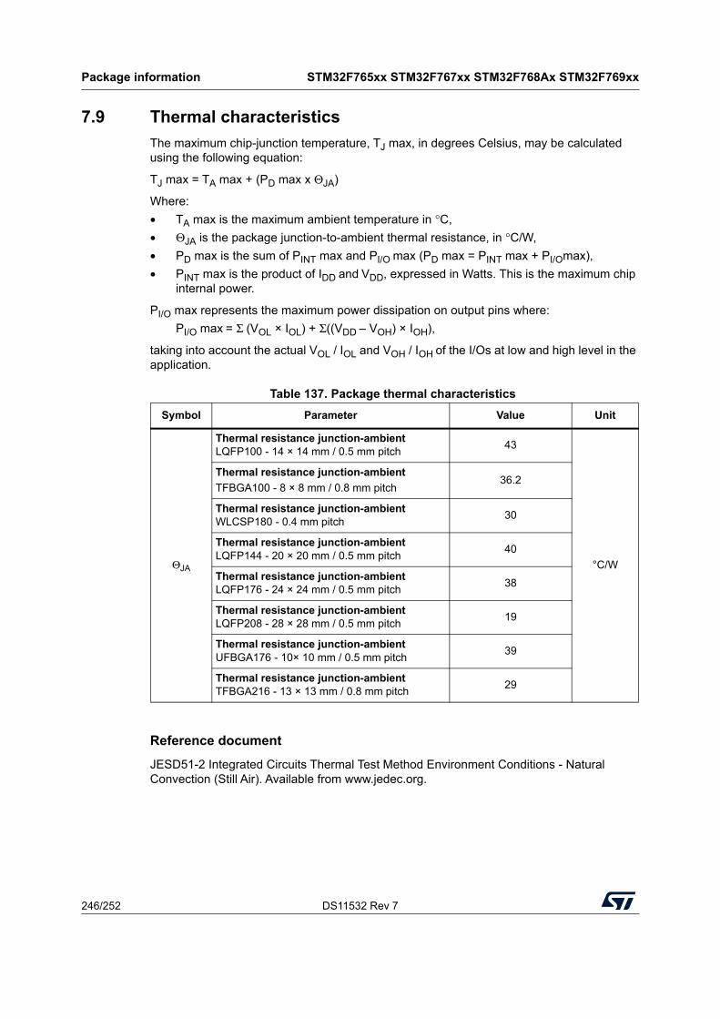
Package information STM32F765xx STM32F767xx STM32F768Ax STM32F769xx
246/252 DS11532 Rev 7
7.9 Thermal characteristics
The maximum chip-junction temperature, TJ max, in degrees Celsius, may be calculated using the following equation:
TJ max = TA max + (PD max x ΘJA)
Where:
• TA max is the maximum ambient temperature in °C,
• ΘJA is the package junction-to-ambient thermal resistance, in °C/W,
• PD max is the sum of PINT max and PI/O max (PD max = PINT max + PI/Omax),
• PINT max is the product of IDD and VDD, expressed in Watts. This is the maximum chip internal power.
PI/O max represents the maximum power dissipation on output pins where:
PI/O max = Σ (VOL × IOL) + Σ((VDD – VOH) × IOH),
taking into account the actual VOL / IOL and VOH / IOH of the I/Os at low and high level in the application.
Reference document
JESD51-2 Integrated Circuits Thermal Test Method Environment Conditions - Natural Convection (Still Air). Available from www.jedec.org.
Table 137. Package thermal characteristics
Symbol Parameter Value Unit
ΘJA
Thermal resistance junction-ambient LQFP100 - 14 × 14 mm / 0.5 mm pitch
43
°C/W
Thermal resistance junction-ambient
TFBGA100 - 8 × 8 mm / 0.8 mm pitch36.2
Thermal resistance junction-ambient WLCSP180 - 0.4 mm pitch
30
Thermal resistance junction-ambient LQFP144 - 20 × 20 mm / 0.5 mm pitch
40
Thermal resistance junction-ambient LQFP176 - 24 × 24 mm / 0.5 mm pitch
38
Thermal resistance junction-ambient LQFP208 - 28 × 28 mm / 0.5 mm pitch
19
Thermal resistance junction-ambient UFBGA176 - 10× 10 mm / 0.5 mm pitch
39
Thermal resistance junction-ambient TFBGA216 - 13 × 13 mm / 0.8 mm pitch
29
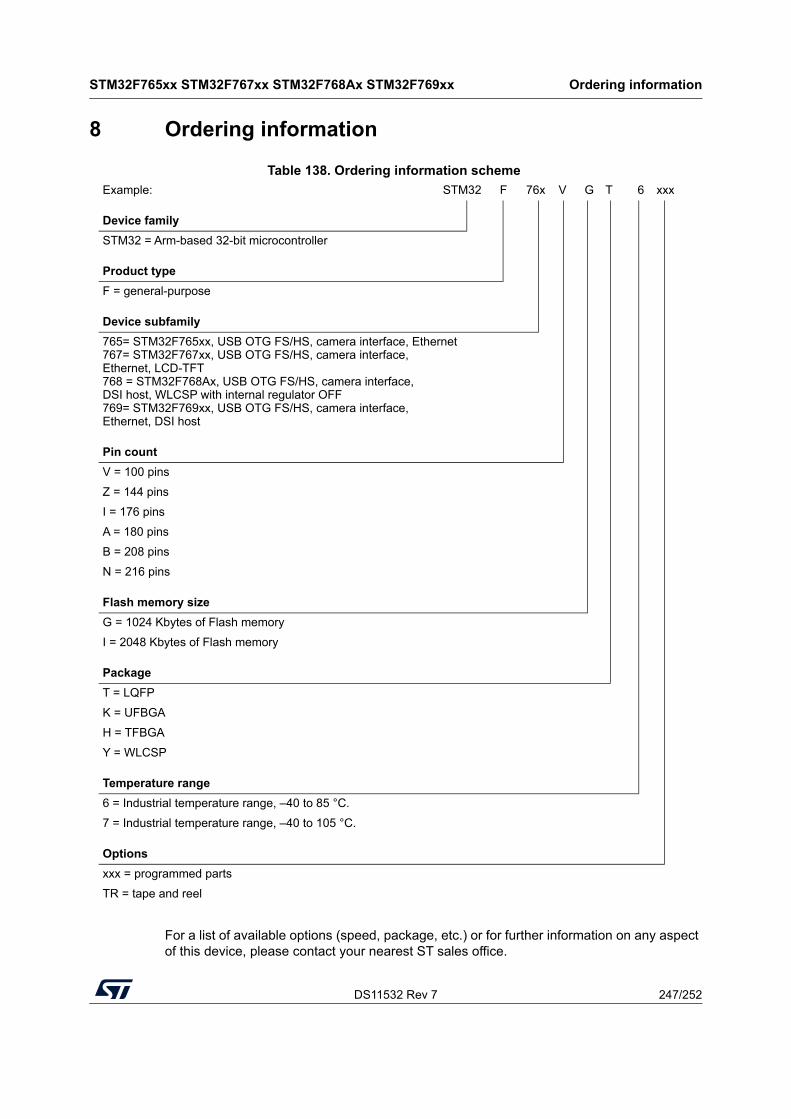
DS11532 Rev 7 247/252
STM32F765xx STM32F767xx STM32F768Ax STM32F769xx Ordering information
251
8 Ordering information
For a list of available options (speed, package, etc.) or for further information on any aspect of this device, please contact your nearest ST sales office.
Table 138. Ordering information scheme
Example: STM32 F 76x V G T 6 xxx
Device family
STM32 = Arm-based 32-bit microcontroller
Product type
F = general-purpose
Device subfamily
765= STM32F765xx, USB OTG FS/HS, camera interface, Ethernet767= STM32F767xx, USB OTG FS/HS, camera interface,Ethernet, LCD-TFT768 = STM32F768Ax, USB OTG FS/HS, camera interface, DSI host, WLCSP with internal regulator OFF769= STM32F769xx, USB OTG FS/HS, camera interface,Ethernet, DSI host
Pin count
V = 100 pins
Z = 144 pins
I = 176 pins
A = 180 pins
B = 208 pins
N = 216 pins
Flash memory size
G = 1024 Kbytes of Flash memory
I = 2048 Kbytes of Flash memory
Package
T = LQFP
K = UFBGA
H = TFBGA
Y = WLCSP
Temperature range
6 = Industrial temperature range, –40 to 85 °C.
7 = Industrial temperature range, –40 to 105 °C.
Options
xxx = programmed parts
TR = tape and reel
Recommendations when using internal reset OFF STM32F765xx STM32F767xx STM32F768Ax
248/252 DS11532 Rev 7
Appendix A Recommendations when using internal reset OFF
When the internal reset is OFF, the following integrated features are no longer supported:
• The integrated power-on reset (POR) / power-down reset (PDR) circuitry is disabled
• The brownout reset (BOR) circuitry must be disabled
• The embedded programmable voltage detector (PVD) is disabled
• VBAT functionality is no more available and VBAT pin should be connected to VDD
• The over-drive mode is not supported
A.1 Operating conditions
Table 139. Limitations depending on the operating power supply range
Operating power supply range
ADC operation
Maximum Flash
memory access
frequency with no wait
states (fFlashmax)
Maximum Flash memory access frequency with wait states (1)(2)
1. Applicable only when the code is executed from Flash memory. When the code is executed from RAM, no wait state is required.
2. Thanks to the ART accelerator on ITCM interface and L1-cache on AXI interface, the number of wait states given here does not impact the execution speed from the Flash memory since the ART accelerator or L1- cache allows to achieve a performance equivalent to 0-wait state program execution.
I/O operationPossible Flash
memory operations
VDD =1.7 to 2.1 V(3)
3. VDD/VDDA minimum value of 1.7 V, with the use of an external power supply supervisor (refer to Section 3.18.1: Internal reset ON).
Conversion time up to 1.2 Msps
20 MHz168 MHz with 8 wait states and over-drive OFF
– No I/O compensation
8-bit erase and program operations only
DS11532 Rev 7 249/252
STM32F765xx STM32F767xx STM32F768Ax STM32F769xx Revision history
251
Revision history
Table 140. Document revision history
Date Revision Changes
21-Mar-2016 1 Initial release.
26-Apr-2016 2
DFSDM replaced by DFSDM1 in:
– Table 11: STM32F765xx, STM32F767xx, STM32F768Ax and STM32F769xx pin and ball definitions.
– Table 13: STM32F765xx, STM32F767xx, STM32F768Ax and STM32F769xx alternate function mapping.
– Section 6.3.34: Digital filter for Sigma-Delta Modulators (DFSDM) characteristics.
Updated Table 2: STM32F765xx, STM32F767xx, STM32F768Ax and STM32F769xx features and peripheral counts adding DFSDM1 features.
Updated Table 39: Peripheral current consumption adding DFSDM1 current consumption.
Updated cover in 2 pages.
Update cover replacing for SPI ‘up to 50 Mbit/s’ by ‘up to 54 Mbit/s’.
06-May-2016 3
Updated Table 2: STM32F765xx, STM32F767xx, STM32F768Ax and STM32F769xx features and peripheral counts GPIO number.
Updated Table 13: STM32F765xx, STM32F767xx, STM32F768Ax and STM32F769xx alternate function mapping adding CAN3_RX alternate function on PA8/AF11.
22-Dec-2016 4
Updated Table 97: Dynamics characteristics: Ethernet MAC signals for RMII.
Updated Table 71: ADC characteristics sampling rate.
Updated all the notes removing ‘not tested in production’.
Updated Figure 46: SPI timing diagram - slave mode and CPHA = 0 and Figure 47: SPI timing diagram - slave mode and CPHA = 1(1) with modified NSS timing waveforms (among other changes).
Updated Table 121: LTDC characteristics clock output frequency at 65 MHz.
Updated Section 6.2: Absolute maximum ratings.
Updated Section 7: Package information adding information about other optional marking or inset/upset marks.
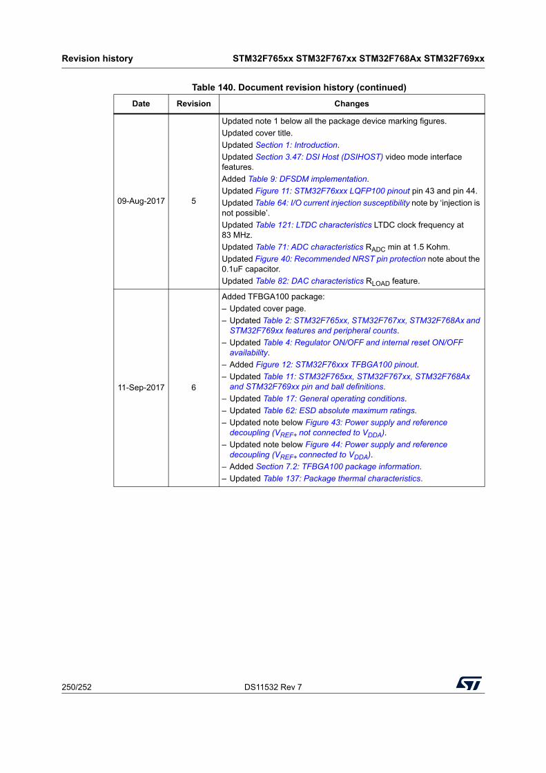
Revision history STM32F765xx STM32F767xx STM32F768Ax STM32F769xx
250/252 DS11532 Rev 7
09-Aug-2017 5
Updated note 1 below all the package device marking figures.
Updated cover title.
Updated Section 1: Introduction.
Updated Section 3.47: DSI Host (DSIHOST) video mode interface features.
Added Table 9: DFSDM implementation.
Updated Figure 11: STM32F76xxx LQFP100 pinout pin 43 and pin 44.
Updated Table 64: I/O current injection susceptibility note by ‘injection is not possible’.
Updated Table 121: LTDC characteristics LTDC clock frequency at 83 MHz.
Updated Table 71: ADC characteristics RADC min at 1.5 Kohm.
Updated Figure 40: Recommended NRST pin protection note about the 0.1uF capacitor.
Updated Table 82: DAC characteristics RLOAD feature.
11-Sep-2017 6
Added TFBGA100 package:
– Updated cover page.
– Updated Table 2: STM32F765xx, STM32F767xx, STM32F768Ax and STM32F769xx features and peripheral counts.
– Updated Table 4: Regulator ON/OFF and internal reset ON/OFF availability.
– Added Figure 12: STM32F76xxx TFBGA100 pinout.
– Updated Table 11: STM32F765xx, STM32F767xx, STM32F768Ax and STM32F769xx pin and ball definitions.
– Updated Table 17: General operating conditions.
– Updated Table 62: ESD absolute maximum ratings.
– Updated note below Figure 43: Power supply and reference decoupling (VREF+ not connected to VDDA).
– Updated note below Figure 44: Power supply and reference decoupling (VREF+ connected to VDDA).
– Added Section 7.2: TFBGA100 package information.
– Updated Table 137: Package thermal characteristics.
Table 140. Document revision history (continued)
Date Revision Changes
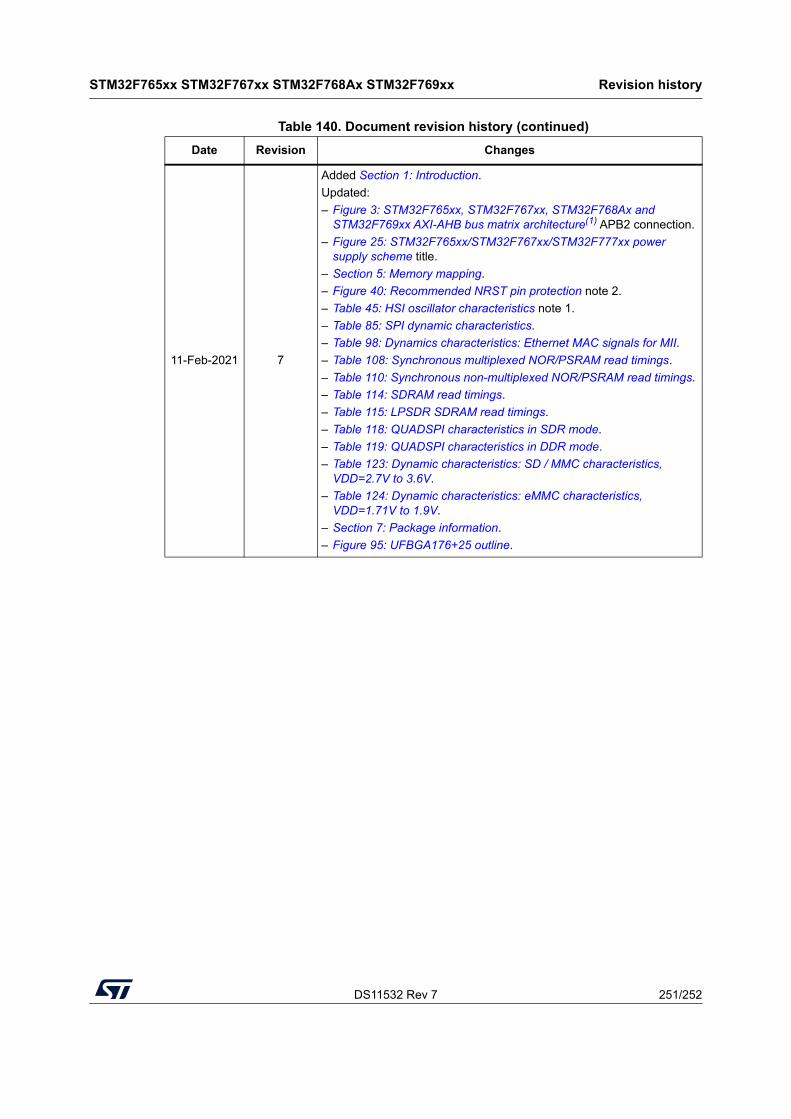
DS11532 Rev 7 251/252
STM32F765xx STM32F767xx STM32F768Ax STM32F769xx Revision history
251
11-Feb-2021 7
Added Section 1: Introduction.
Updated:
– Figure 3: STM32F765xx, STM32F767xx, STM32F768Ax and STM32F769xx AXI-AHB bus matrix architecture(1) APB2 connection.
– Figure 25: STM32F765xx/STM32F767xx/STM32F777xx power supply scheme title.
– Section 5: Memory mapping.
– Figure 40: Recommended NRST pin protection note 2.
– Table 45: HSI oscillator characteristics note 1.
– Table 85: SPI dynamic characteristics.
– Table 98: Dynamics characteristics: Ethernet MAC signals for MII.
– Table 108: Synchronous multiplexed NOR/PSRAM read timings.
– Table 110: Synchronous non-multiplexed NOR/PSRAM read timings.
– Table 114: SDRAM read timings.
– Table 115: LPSDR SDRAM read timings.
– Table 118: QUADSPI characteristics in SDR mode.
– Table 119: QUADSPI characteristics in DDR mode.
– Table 123: Dynamic characteristics: SD / MMC characteristics, VDD=2.7V to 3.6V.
– Table 124: Dynamic characteristics: eMMC characteristics, VDD=1.71V to 1.9V.
– Section 7: Package information.
– Figure 95: UFBGA176+25 outline.
Table 140. Document revision history (continued)
Date Revision Changes
STM32F765xx STM32F767xx STM32F768Ax STM32F769xx
252/252 DS11532 Rev 7
IMPORTANT NOTICE – PLEASE READ CAREFULLY
STMicroelectronics NV and its subsidiaries (“ST”) reserve the right to make changes, corrections, enhancements, modifications, and improvements to ST products and/or to this document at any time without notice. Purchasers should obtain the latest relevant information on ST products before placing orders. ST products are sold pursuant to ST’s terms and conditions of sale in place at the time of order acknowledgement.
Purchasers are solely responsible for the choice, selection, and use of ST products and ST assumes no liability for application assistance or the design of Purchasers’ products.
No license, express or implied, to any intellectual property right is granted by ST herein.
Resale of ST products with provisions different from the information set forth herein shall void any warranty granted by ST for such product.
ST and the ST logo are trademarks of ST. For additional information about ST trademarks, please refer to www.st.com/trademarks. All other product or service names are the property of their respective owners.
Information in this document supersedes and replaces information previously supplied in any prior versions of this document.
© 2021 STMicroelectronics – All rights reserved


![Modular Connected [2MB]](https://img.pdfslide.net/doc/110x75/58a2f86c1a28ab8e608c1e28/modular-connected-2mb.jpg)