Embed Size (px)
Citation preview
ARM Processors and Architectures
Tratto in parte da
ARM University Program
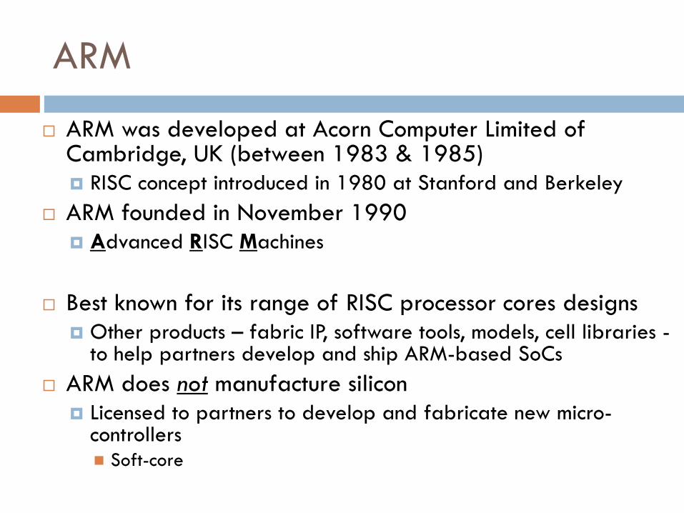
ARM
ARM was developed at Acorn Computer Limited of Cambridge, UK (between 1983 & 1985)
RISC concept introduced in 1980 at Stanford and Berkeley
ARM founded in November 1990
Advanced RISC Machines
Best known for its range of RISC processor cores designs
Other products – fabric IP, software tools, models, cell libraries - to help partners develop and ship ARM-based SoCs
ARM does not manufacture silicon
Licensed to partners to develop and fabricate new micro-controllers Soft-core
ARM architecture
Based upon RISC Architecture with enhancements to
meet requirements of embedded applications
A large uniform register file
Load-store architecture
Fixed length instructions
32-bit processor (v1-v7), 64-bit processor (v8)
Good speed/power
High code density
Enhancement to Basic RISC
Control over both ALU and shifter for every data
processing operations
Auto-increment and auto-decrement addressing
modes
To optimize program loops
Load/Store multiple data instructions
To maximize data throughput
Conditional execution of instructions
To maximize execution throughput
Embedded Processors
Application Processors
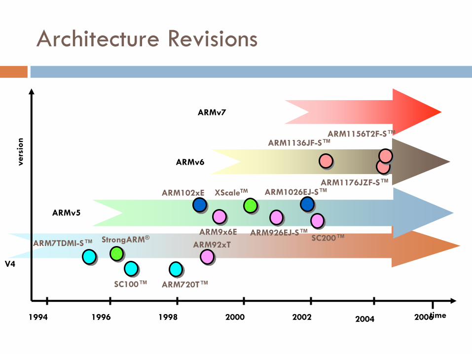
Architecture Revisions
1998 2000 2002 2004 time
vers
ion
ARMv5
ARMv6
1994 1996 2006
V4
StrongARM® ARM926EJ-S™
XScaleTM ARM102xE ARM1026EJ-S™
ARM9x6E
ARM92xT
ARM1136JF-S™
ARM7TDMI-S™
ARM720T™
ARMv7
SC100™
SC200™
ARM1176JZF-S™
ARM1156T2F-S™
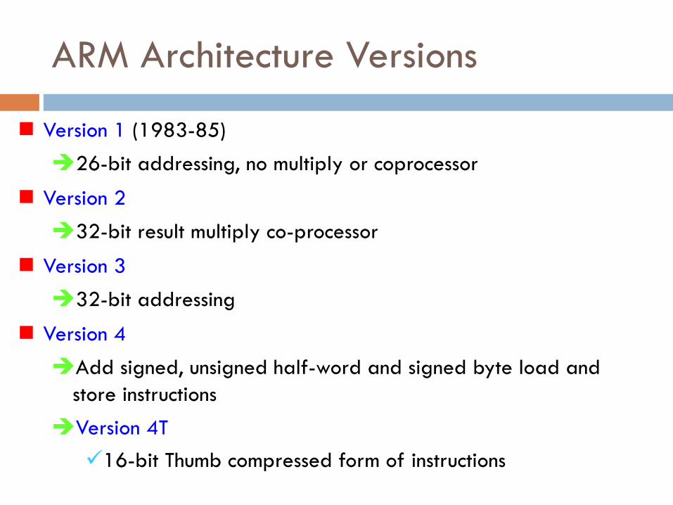
ARM Architecture Versions
Version 1 (1983-85)
26-bit addressing, no multiply or coprocessor
Version 2
32-bit result multiply co-processor
Version 3
32-bit addressing
Version 4
Add signed, unsigned half-word and signed byte load and
store instructions
Version 4T
16-bit Thumb compressed form of instructions
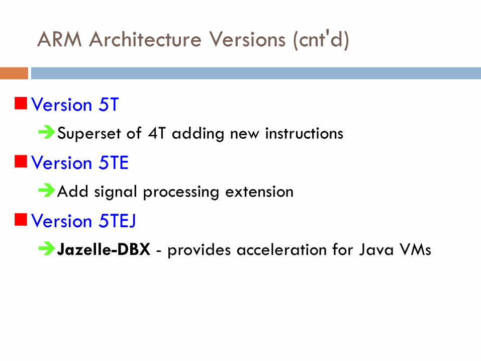
ARM Architecture Versions (cnt'd)
Version 5T
Superset of 4T adding new instructions
Version 5TE
Add signal processing extension
Version 5TEJ
Jazelle-DBX - provides acceleration for Java VMs
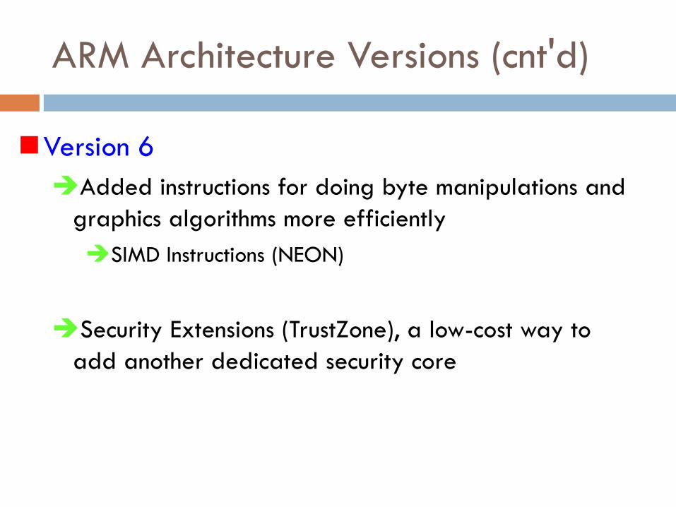
ARM Architecture Versions (cnt'd)
Version 6
Added instructions for doing byte manipulations and
graphics algorithms more efficiently
SIMD Instructions (NEON)
Security Extensions (TrustZone), a low-cost way to
add another dedicated security core
ARM Architecture Versions (cnt'd)
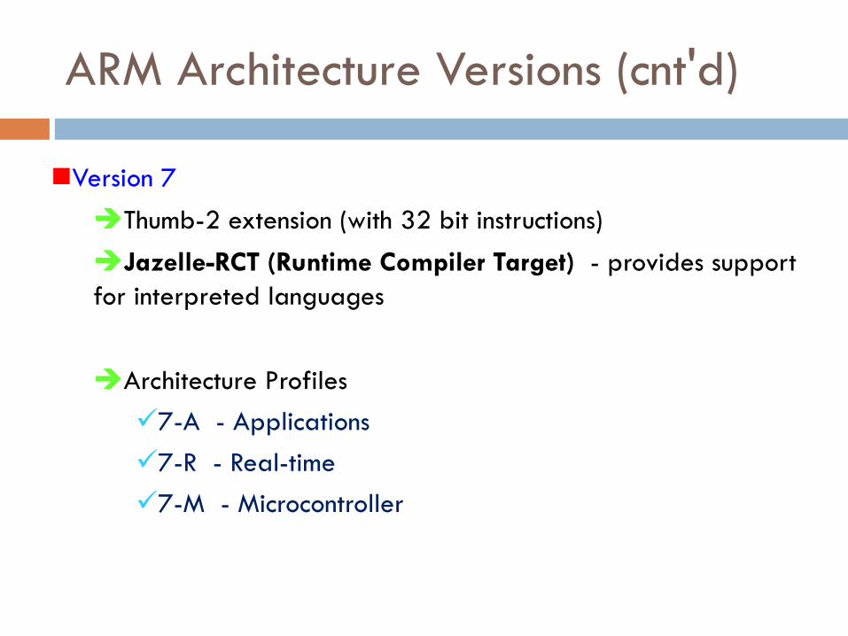
Version 7
Thumb-2 extension (with 32 bit instructions)
Jazelle-RCT (Runtime Compiler Target) - provides support
for interpreted languages
Architecture Profiles
7-A - Applications
7-R - Real-time
7-M - Microcontroller
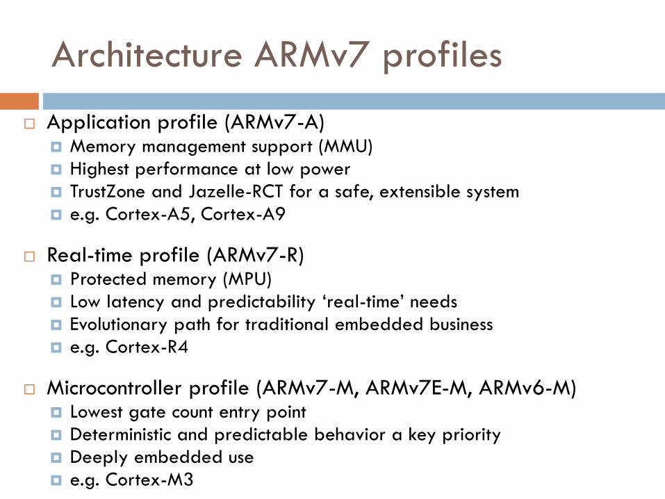
Architecture ARMv7 profiles
Application profile (ARMv7-A) Memory management support (MMU)
Highest performance at low power
TrustZone and Jazelle-RCT for a safe, extensible system
e.g. Cortex-A5, Cortex-A9
Real-time profile (ARMv7-R) Protected memory (MPU)
Low latency and predictability ‘real-time’ needs
Evolutionary path for traditional embedded business
e.g. Cortex-R4
Microcontroller profile (ARMv7-M, ARMv7E-M, ARMv6-M) Lowest gate count entry point
Deterministic and predictable behavior a key priority
Deeply embedded use
e.g. Cortex-M3
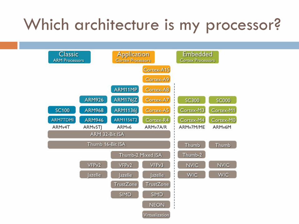
Which architecture is my processor?
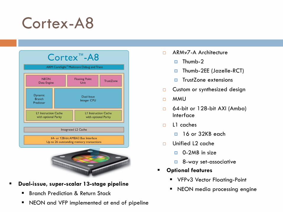
Cortex-A8
ARMv7-A Architecture
Thumb-2
Thumb-2EE (Jazelle-RCT)
TrustZone extensions
Custom or synthesized design
MMU
64-bit or 128-bit AXI (Amba) Interface
L1 caches
16 or 32KB each
Unified L2 cache
0-2MB in size
8-way set-associative
Optional features
VFPv3 Vector Floating-Point
NEON media processing engine
Dual-issue, super-scalar 13-stage pipeline
Branch Prediction & Return Stack
NEON and VFP implemented at end of pipeline
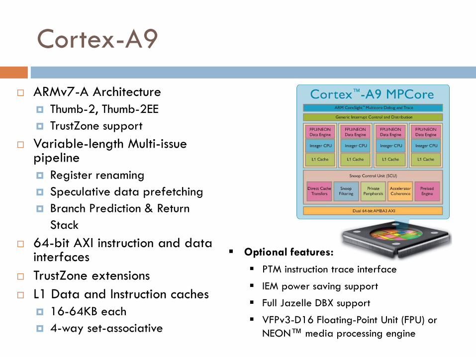
Cortex-A9
ARMv7-A Architecture
Thumb-2, Thumb-2EE
TrustZone support
Variable-length Multi-issue pipeline
Register renaming
Speculative data prefetching
Branch Prediction & Return
Stack
64-bit AXI instruction and data interfaces
TrustZone extensions
L1 Data and Instruction caches
16-64KB each
4-way set-associative
Optional features:
PTM instruction trace interface
IEM power saving support
Full Jazelle DBX support
VFPv3-D16 Floating-Point Unit (FPU) or
NEON™ media processing engine
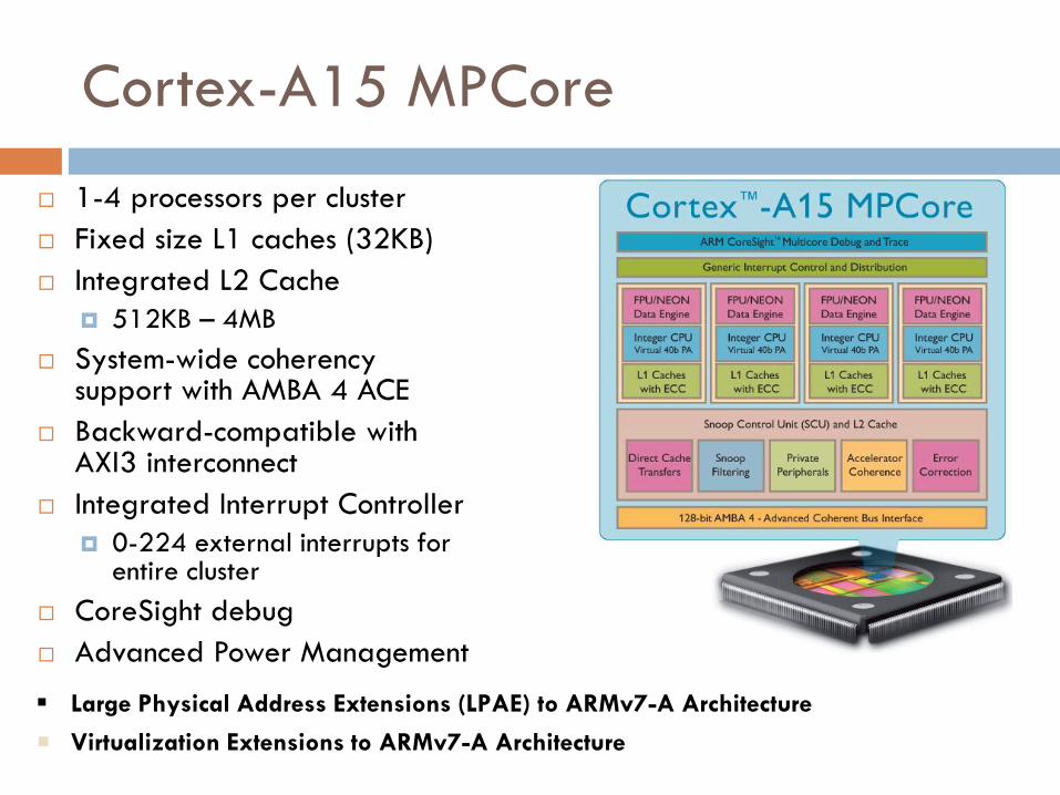
Cortex-A15 MPCore
1-4 processors per cluster
Fixed size L1 caches (32KB)
Integrated L2 Cache
512KB – 4MB
System-wide coherency support with AMBA 4 ACE
Backward-compatible with AXI3 interconnect
Integrated Interrupt Controller
0-224 external interrupts for entire cluster
CoreSight debug
Advanced Power Management
Large Physical Address Extensions (LPAE) to ARMv7-A Architecture
Virtualization Extensions to ARMv7-A Architecture
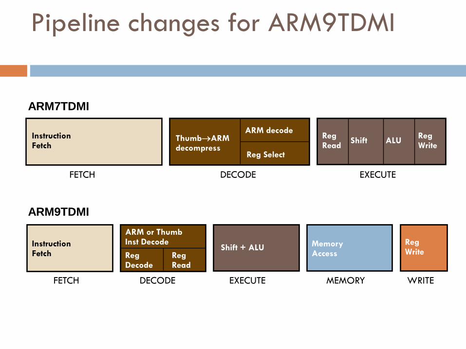
Pipeline changes for ARM9TDMI
Instruction Fetch
Shift + ALU Memory Access
Reg Write Reg
Read Reg Decode
FETCH DECODE EXECUTE MEMORY WRITE
ARM9TDMI
ARM or Thumb Inst Decode
Reg Select
Reg Read
Shift ALU Reg Write
ThumbARM decompress
ARM decode Instruction Fetch
FETCH DECODE EXECUTE
ARM7TDMI
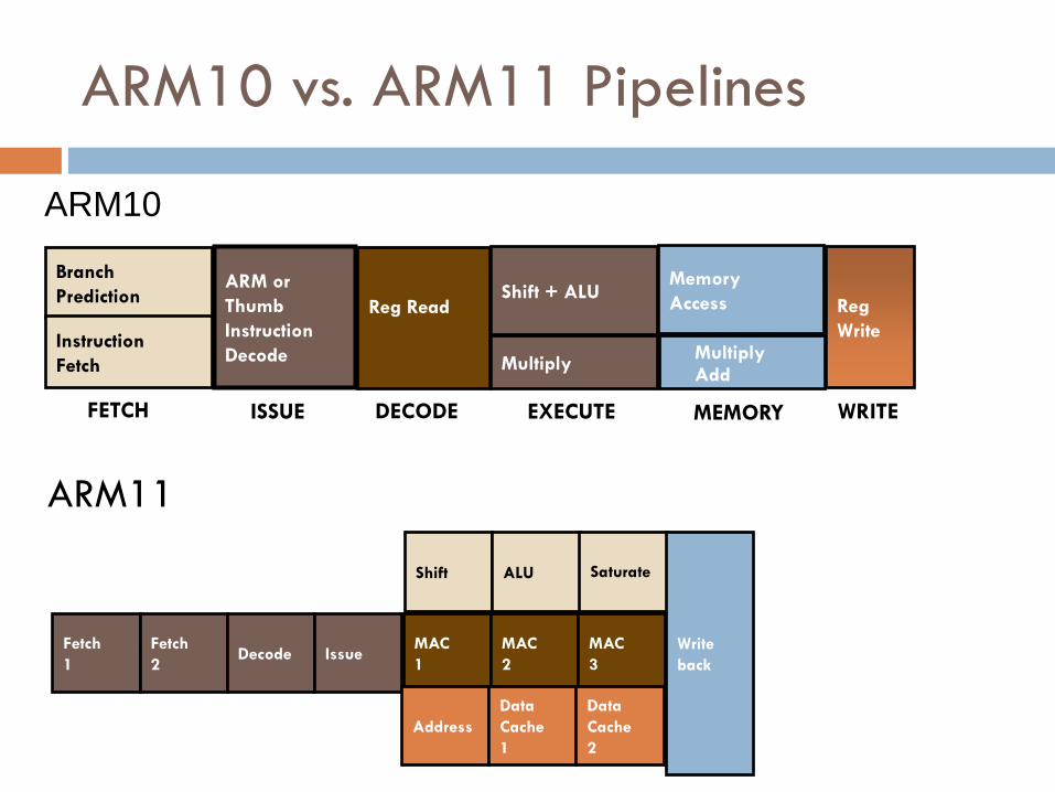
ARM10 vs. ARM11 Pipelines
ARM11
Fetch
1
Fetch
2 Decode Issue
Shift ALU Saturate
Write
back
MAC
1
MAC
2
MAC
3
Address
Data
Cache
1
Data
Cache
2
Shift + ALU Memory
Access Reg
Write
FETCH DECODE EXECUTE MEMORY WRITE
Reg Read
Multiply
Branch
Prediction
Instruction
Fetch
ISSUE
ARM or
Thumb
Instruction
Decode Multiply Add
ARM10
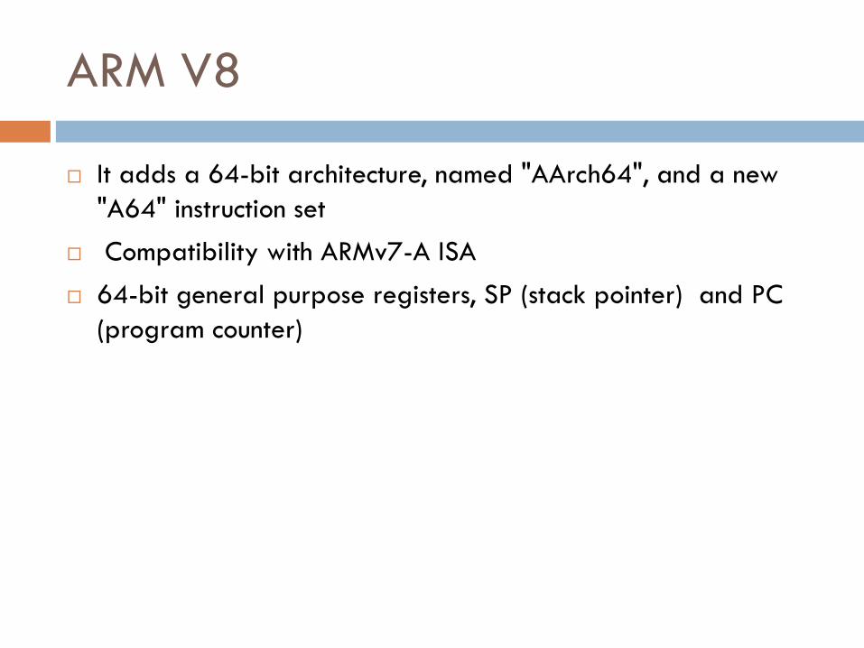
ARM V8
It adds a 64-bit architecture, named "AArch64", and a new
"A64" instruction set
Compatibility with ARMv7-A ISA
64-bit general purpose registers, SP (stack pointer) and PC
(program counter)
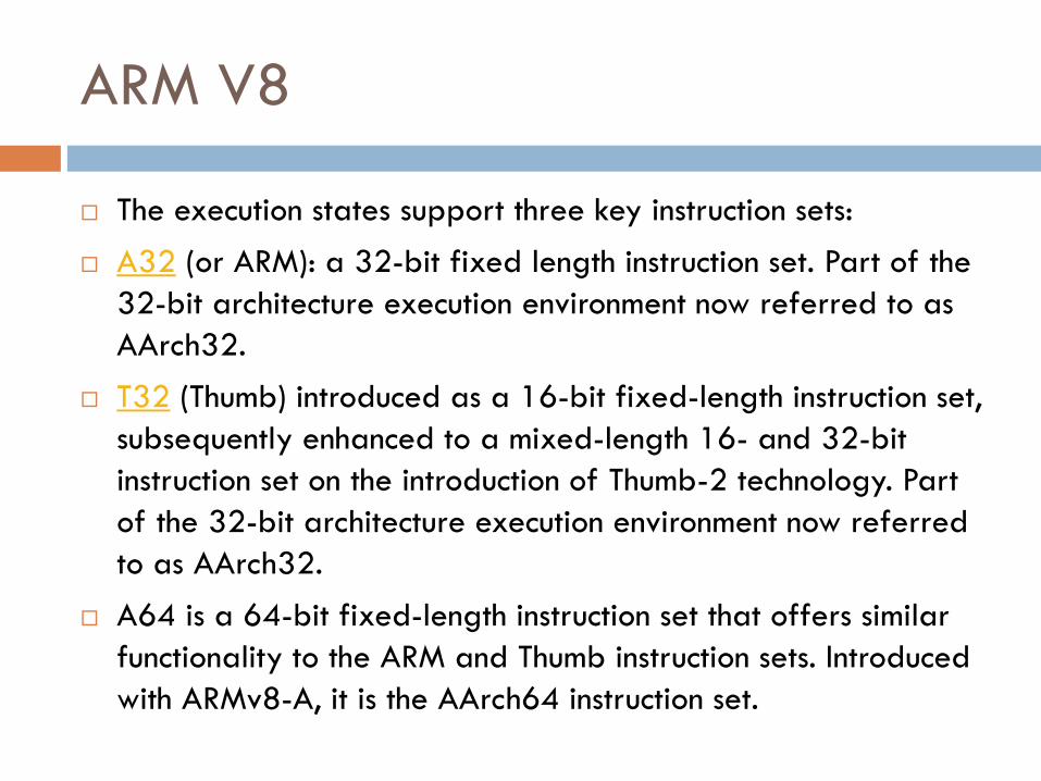
ARM V8
The execution states support three key instruction sets:
A32 (or ARM): a 32-bit fixed length instruction set. Part of the
32-bit architecture execution environment now referred to as
AArch32.
T32 (Thumb) introduced as a 16-bit fixed-length instruction set,
subsequently enhanced to a mixed-length 16- and 32-bit
instruction set on the introduction of Thumb-2 technology. Part
of the 32-bit architecture execution environment now referred
to as AArch32.
A64 is a 64-bit fixed-length instruction set that offers similar
functionality to the ARM and Thumb instruction sets. Introduced
with ARMv8-A, it is the AArch64 instruction set.
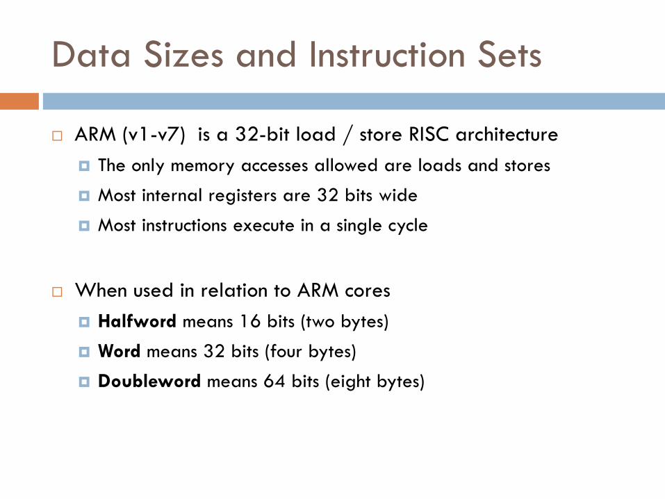
Data Sizes and Instruction Sets
ARM (v1-v7) is a 32-bit load / store RISC architecture
The only memory accesses allowed are loads and stores
Most internal registers are 32 bits wide
Most instructions execute in a single cycle
When used in relation to ARM cores
Halfword means 16 bits (two bytes)
Word means 32 bits (four bytes)
Doubleword means 64 bits (eight bytes)
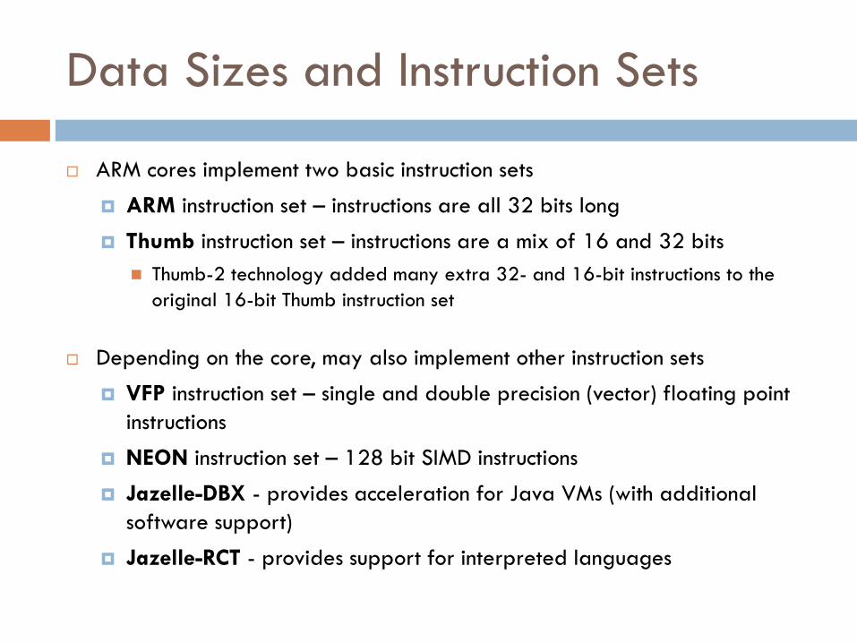
Data Sizes and Instruction Sets
ARM cores implement two basic instruction sets
ARM instruction set – instructions are all 32 bits long
Thumb instruction set – instructions are a mix of 16 and 32 bits
Thumb-2 technology added many extra 32- and 16-bit instructions to the
original 16-bit Thumb instruction set
Depending on the core, may also implement other instruction sets
VFP instruction set – single and double precision (vector) floating point
instructions
NEON instruction set – 128 bit SIMD instructions
Jazelle-DBX - provides acceleration for Java VMs (with additional
software support)
Jazelle-RCT - provides support for interpreted languages
Core Data Path
Data items are placed in register file
No data processing instructions directly manipulate
data in memory
Instructions typically use two source registers and a
single destination register
A barrel shifter on the data path can preprocess
data before it enters ALU
Increment/decrement logic can update register
content for sequential access independent of ALU
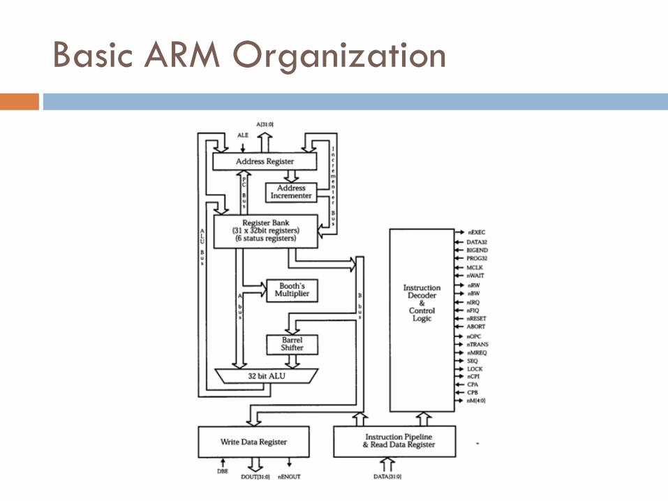
Basic ARM Organization
Registers
General Purpose registers hold either data or address
All registers are of 32 bits
In user mode 16 data registers and 2 status registers are visible
Data registers: r0 to r15
r13, r14, and r15 perform special functions
r13: stack pointer
r14: link register
r15: program counter
Registers
Depending upon context, registers r13 and r14 can
also be used as GPR
Two status registers
CPSR: Current Program Status Register
SPSR: Saved Program Status Register
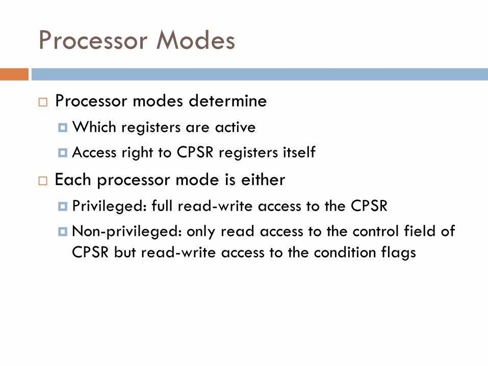
Processor Modes
Processor modes determine
Which registers are active
Access right to CPSR registers itself
Each processor mode is either
Privileged: full read-write access to the CPSR
Non-privileged: only read access to the control field of
CPSR but read-write access to the condition flags
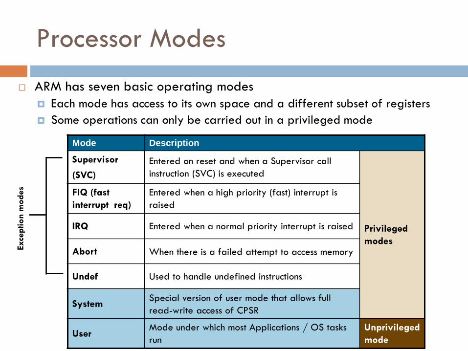
Processor Modes
ARM has seven basic operating modes
Each mode has access to its own space and a different subset of registers
Some operations can only be carried out in a privileged mode
Mode Description
Supervisor
(SVC)
Entered on reset and when a Supervisor call
instruction (SVC) is executed
Privileged
modes
FIQ (fast
interrupt req)
Entered when a high priority (fast) interrupt is
raised
IRQ Entered when a normal priority interrupt is raised
Abort When there is a failed attempt to access memory
Undef Used to handle undefined instructions
System Special version of user mode that allows full
read-write access of CPSR
User Mode under which most Applications / OS tasks
run
Unprivileged
mode
Exce
ption m
odes
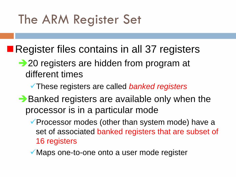
The ARM Register Set
Register files contains in all 37 registers
20 registers are hidden from program at
different times
These registers are called banked registers
Banked registers are available only when the
processor is in a particular mode
Processor modes (other than system mode) have a
set of associated banked registers that are subset of
16 registers
Maps one-to-one onto a user mode register
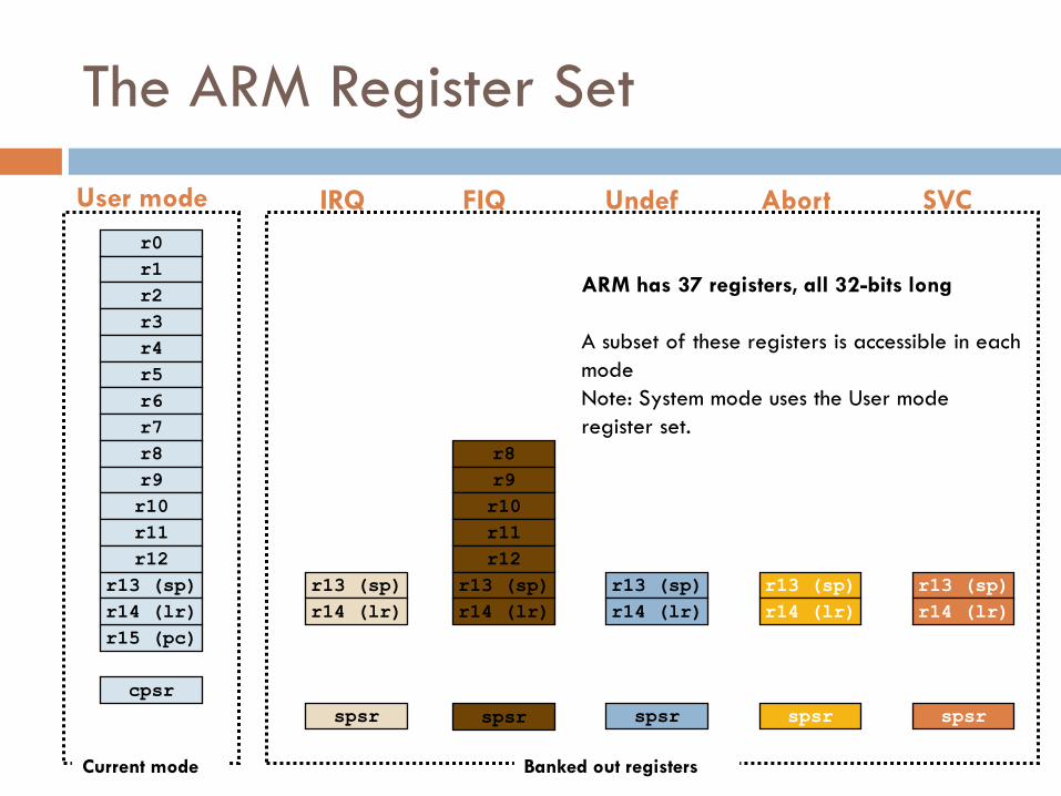
The ARM Register Set
r0
r1
r2
r3
r4
r5
r6
r7
r8
r9
r10
r11
r12
r15 (pc)
cpsr
r13 (sp)
r14 (lr)
User mode
spsr
r13 (sp)
r14 (lr)
IRQ FIQ
r8
r9
r10
r11
r12
r13 (sp)
r14 (lr)
spsr spsr
r13 (sp)
r14 (lr)
Undef
spsr
r13 (sp)
r14 (lr)
Abort
spsr
r13 (sp)
r14 (lr)
SVC
Current mode Banked out registers
ARM has 37 registers, all 32-bits long
A subset of these registers is accessible in each
mode
Note: System mode uses the User mode
register set.
SPSR
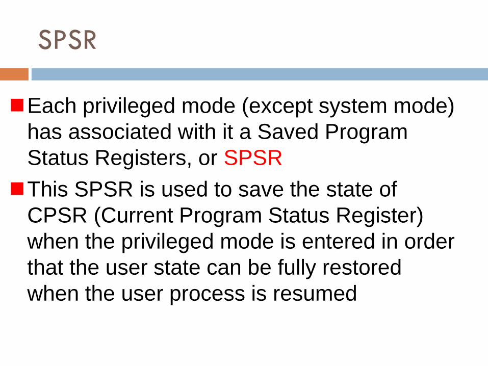
Each privileged mode (except system mode)
has associated with it a Saved Program
Status Registers, or SPSR
This SPSR is used to save the state of
CPSR (Current Program Status Register)
when the privileged mode is entered in order
that the user state can be fully restored
when the user process is resumed
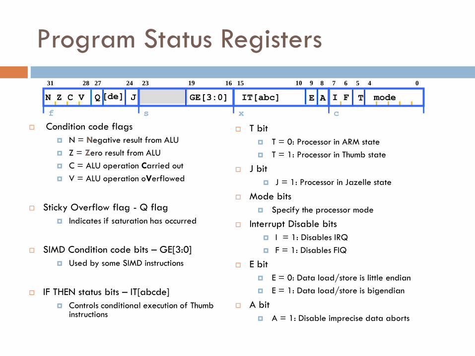
Program Status Registers
Condition code flags
N = Negative result from ALU
Z = Zero result from ALU
C = ALU operation Carried out
V = ALU operation oVerflowed
Sticky Overflow flag - Q flag
Indicates if saturation has occurred
SIMD Condition code bits – GE[3:0]
Used by some SIMD instructions
IF THEN status bits – IT[abcde]
Controls conditional execution of Thumb instructions
T bit
T = 0: Processor in ARM state
T = 1: Processor in Thumb state
J bit
J = 1: Processor in Jazelle state
Mode bits
Specify the processor mode
Interrupt Disable bits
I = 1: Disables IRQ
F = 1: Disables FIQ
E bit
E = 0: Data load/store is little endian
E = 1: Data load/store is bigendian
A bit
A = 1: Disable imprecise data aborts
f s x c
27 31 28 6 7 16 23
15
5 4 0 24
J
10 8 9 19
Q T I F mode N Z C V IT[abc] [de] E A GE[3:0]
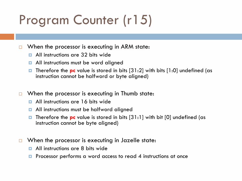
When the processor is executing in ARM state:
All instructions are 32 bits wide
All instructions must be word aligned
Therefore the pc value is stored in bits [31:2] with bits [1:0] undefined (as instruction cannot be halfword or byte aligned)
When the processor is executing in Thumb state:
All instructions are 16 bits wide
All instructions must be halfword aligned
Therefore the pc value is stored in bits [31:1] with bit [0] undefined (as instruction cannot be byte aligned)
When the processor is executing in Jazelle state:
All instructions are 8 bits wide
Processor performs a word access to read 4 instructions at once
Program Counter (r15)
Mode Changing
Mode changes by writing directly to CPSR or by
hardware when the processor responds to exception or
interrupt
To return to user mode a special return instruction is used
that instructs the core to restore the original CPSR and
banked registers
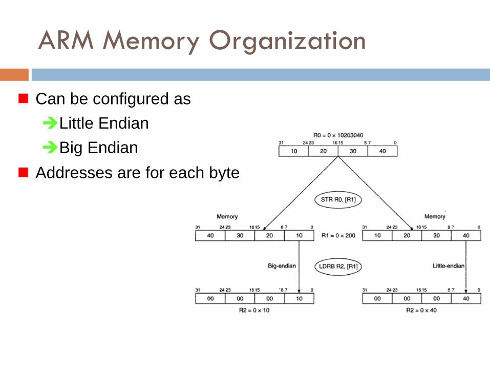
ARM Memory Organization
Can be configured as
Little Endian
Big Endian
Addresses are for each byte
ARM Instruction Set
Instruction Set basics
The ARM Architecture is a Load/Store architecture
No direct manipulation of memory contents
Memory must be loaded into the CPU to be modified, then written back out
Cores are either in ARM state or Thumb state
This determines which instruction set is being executed
An instruction must be executed to switch between states
The architecture allows programmers and compilation tools to reduce branching through the use of conditional execution
Method differs between ARM and Thumb, but the principle is that most (ARM) or all (Thumb) instructions can be executed conditionally.
Instructions
Instruction process data held in registers
and access memory with load and store
instructions
Classes of instructions
Data processing
Branch instructions
Load-store instructions
Software interrupt instruction
Program status register instructions
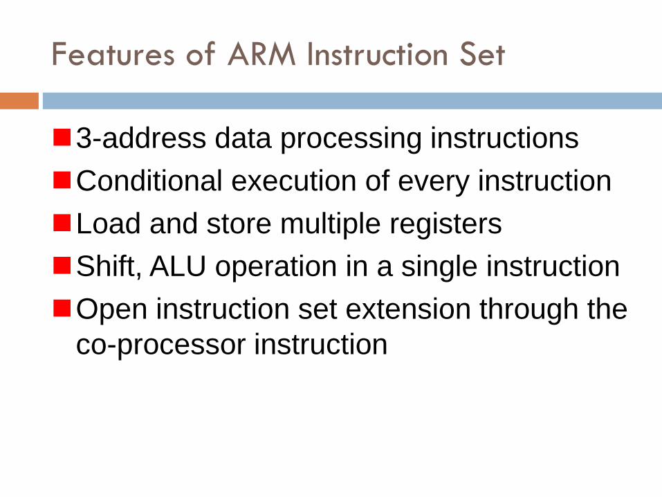
Features of ARM Instruction Set
3-address data processing instructions
Conditional execution of every instruction
Load and store multiple registers
Shift, ALU operation in a single instruction
Open instruction set extension through the
co-processor instruction
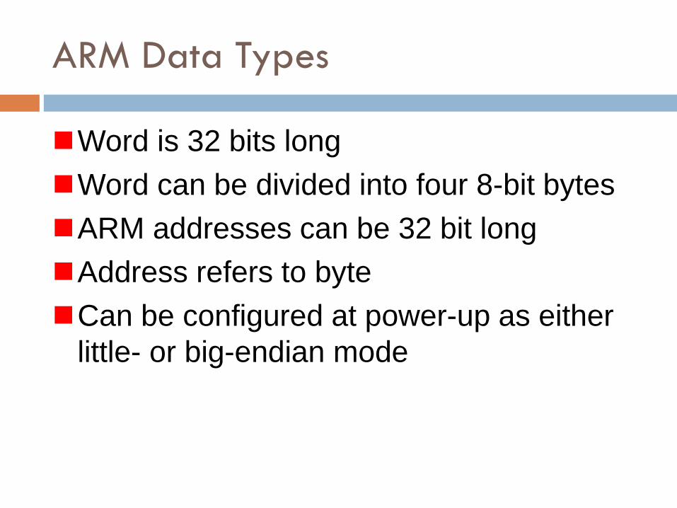
ARM Data Types
Word is 32 bits long
Word can be divided into four 8-bit bytes
ARM addresses can be 32 bit long
Address refers to byte
Can be configured at power-up as either
little- or big-endian mode
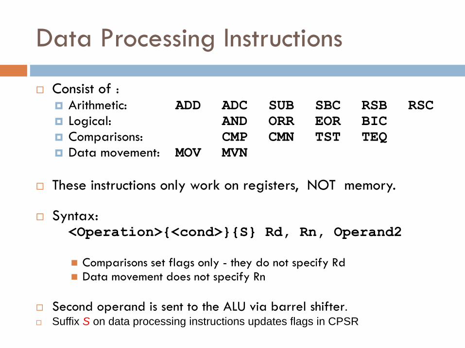
Data Processing Instructions
Consist of : Arithmetic: ADD ADC SUB SBC RSB RSC
Logical: AND ORR EOR BIC
Comparisons: CMP CMN TST TEQ
Data movement: MOV MVN
These instructions only work on registers, NOT memory.
Syntax: <Operation>{<cond>}{S} Rd, Rn, Operand2
Comparisons set flags only - they do not specify Rd Data movement does not specify Rn
Second operand is sent to the ALU via barrel shifter.
Suffix S on data processing instructions updates flags in CPSR
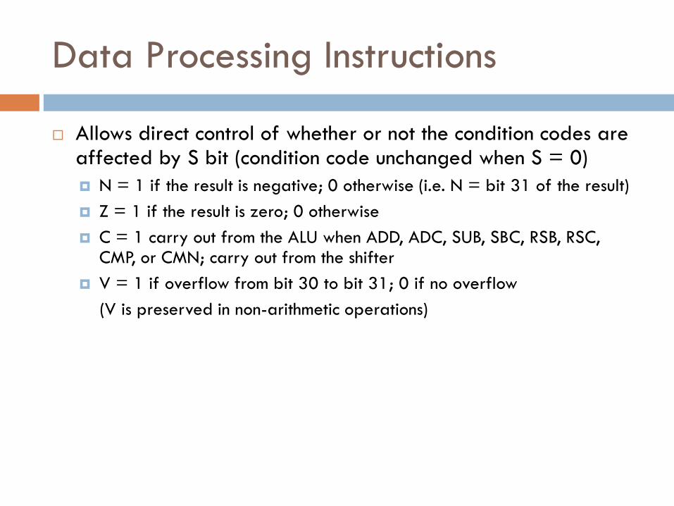
Data Processing Instructions
Allows direct control of whether or not the condition codes are affected by S bit (condition code unchanged when S = 0)
N = 1 if the result is negative; 0 otherwise (i.e. N = bit 31 of the result)
Z = 1 if the result is zero; 0 otherwise
C = 1 carry out from the ALU when ADD, ADC, SUB, SBC, RSB, RSC, CMP, or CMN; carry out from the shifter
V = 1 if overflow from bit 30 to bit 31; 0 if no overflow
(V is preserved in non-arithmetic operations)
Data Processing Instructions
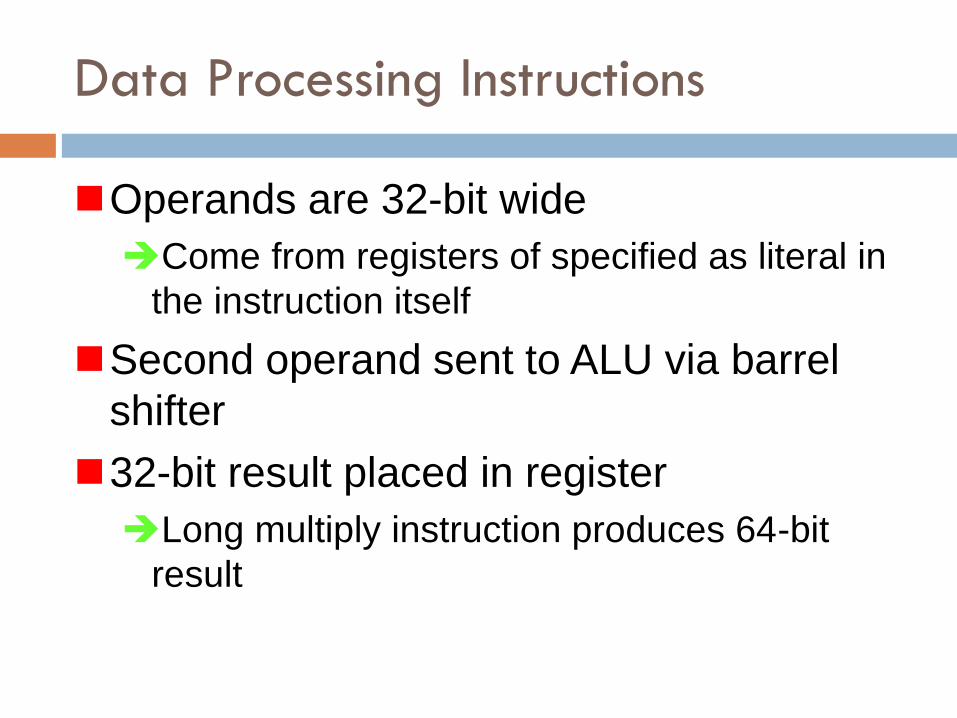
Operands are 32-bit wide
Come from registers of specified as literal in
the instruction itself
Second operand sent to ALU via barrel
shifter
32-bit result placed in register
Long multiply instruction produces 64-bit
result
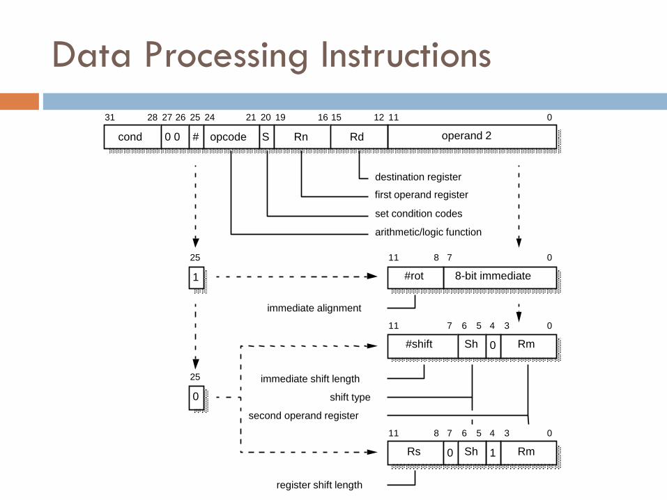
Data Processing Instructions
cond 0 0 operand 2 # opcode S Rn Rd
31 28 27 26 25 24 21 20 19 16 15 12 1 1 0
destination register
first operand register
set condition codes
arithmetic/logic function
8-bit immediate 1
25 1 1 8 7 0
#rot
Rm
1 1 7 6 5 4 3 0
#shift
Rm
0
25
1 1 8 7 6 5 4 3 0
Rs
Sh 0
1 0 Sh
immediate alignment
immediate shift length
shift type
second operand register
register shift length
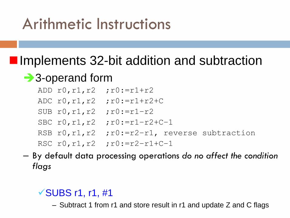
Arithmetic Instructions
Implements 32-bit addition and subtraction
3-operand form ADD r0,r1,r2 ;r0:=r1+r2
ADC r0,r1,r2 ;r0:=r1+r2+C
SUB r0,r1,r2 ;r0:=r1–r2
SBC r0,r1,r2 ;r0:=r1–r2+C–1
RSB r0,r1,r2 ;r0:=r2–r1, reverse subtraction
RSC r0,r1,r2 ;r0:=r2–r1+C–1
– By default data processing operations do no affect the condition flags
SUBS r1, r1, #1 – Subtract 1 from r1 and store result in r1 and update Z and C flags
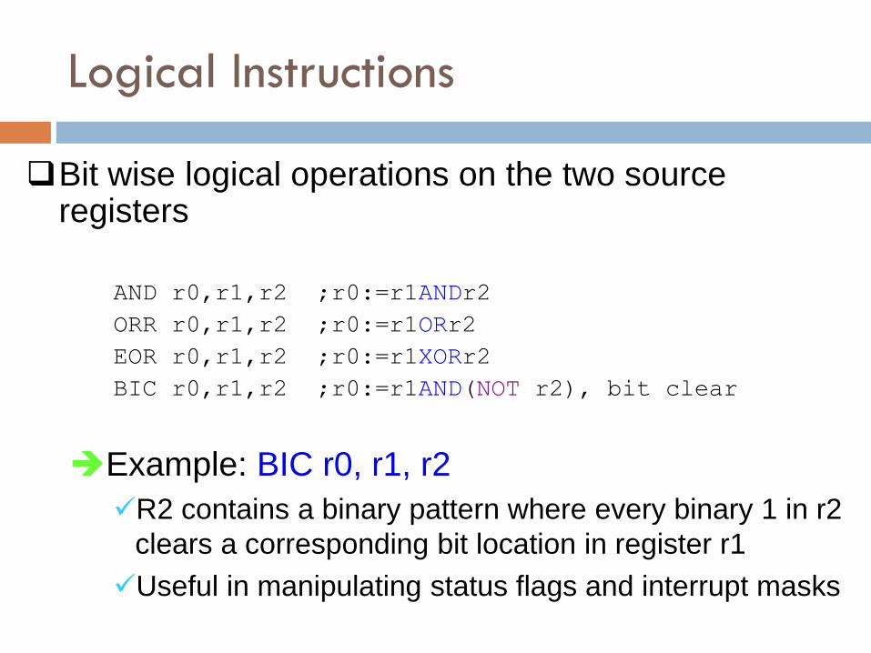
Logical Instructions
Bit wise logical operations on the two source registers
AND r0,r1,r2 ;r0:=r1ANDr2
ORR r0,r1,r2 ;r0:=r1ORr2
EOR r0,r1,r2 ;r0:=r1XORr2
BIC r0,r1,r2 ;r0:=r1AND(NOT r2), bit clear
Example: BIC r0, r1, r2
R2 contains a binary pattern where every binary 1 in r2
clears a corresponding bit location in register r1
Useful in manipulating status flags and interrupt masks
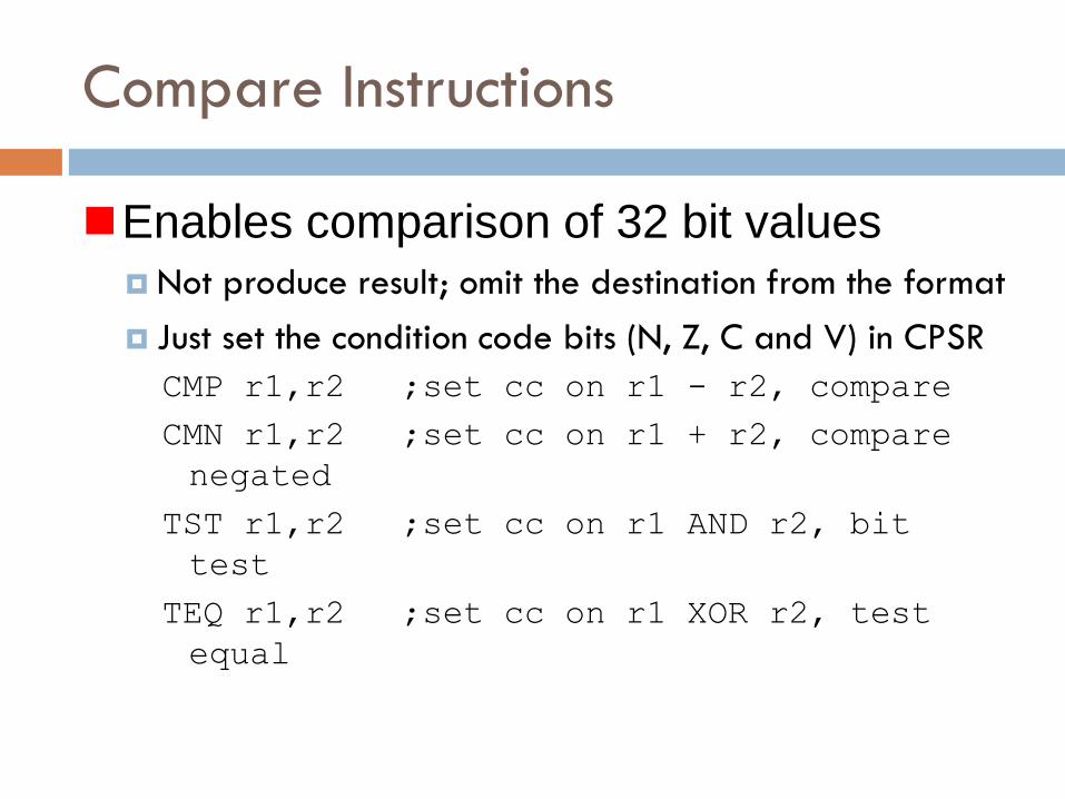
Compare Instructions
Enables comparison of 32 bit values
Not produce result; omit the destination from the format
Just set the condition code bits (N, Z, C and V) in CPSR
CMP r1,r2 ;set cc on r1 - r2, compare
CMN r1,r2 ;set cc on r1 + r2, compare
negated
TST r1,r2 ;set cc on r1 AND r2, bit
test
TEQ r1,r2 ;set cc on r1 XOR r2, test
equal
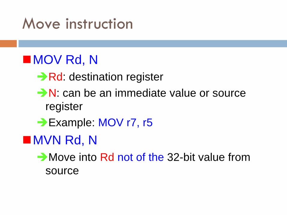
Move instruction
MOV Rd, N
Rd: destination register
N: can be an immediate value or source
register
Example: MOV r7, r5
MVN Rd, N
Move into Rd not of the 32-bit value from
source
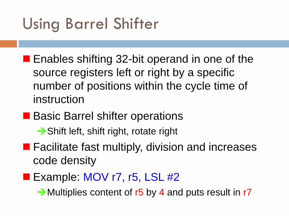
Using Barrel Shifter
Enables shifting 32-bit operand in one of the
source registers left or right by a specific
number of positions within the cycle time of
instruction
Basic Barrel shifter operations
Shift left, shift right, rotate right
Facilitate fast multiply, division and increases
code density
Example: MOV r7, r5, LSL #2
Multiplies content of r5 by 4 and puts result in r7
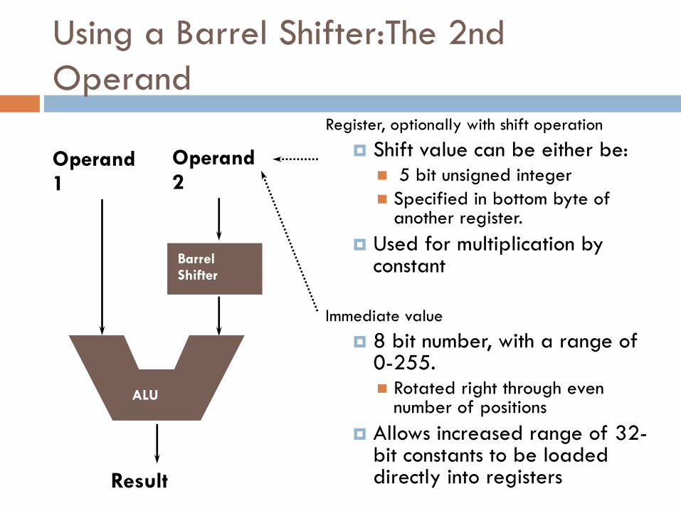
Register, optionally with shift operation
Shift value can be either be: 5 bit unsigned integer
Specified in bottom byte of another register.
Used for multiplication by constant
Immediate value
8 bit number, with a range of 0-255. Rotated right through even
number of positions
Allows increased range of 32-bit constants to be loaded directly into registers
Result
Operand 1
Barrel Shifter
Operand 2
ALU
Using a Barrel Shifter:The 2nd
Operand
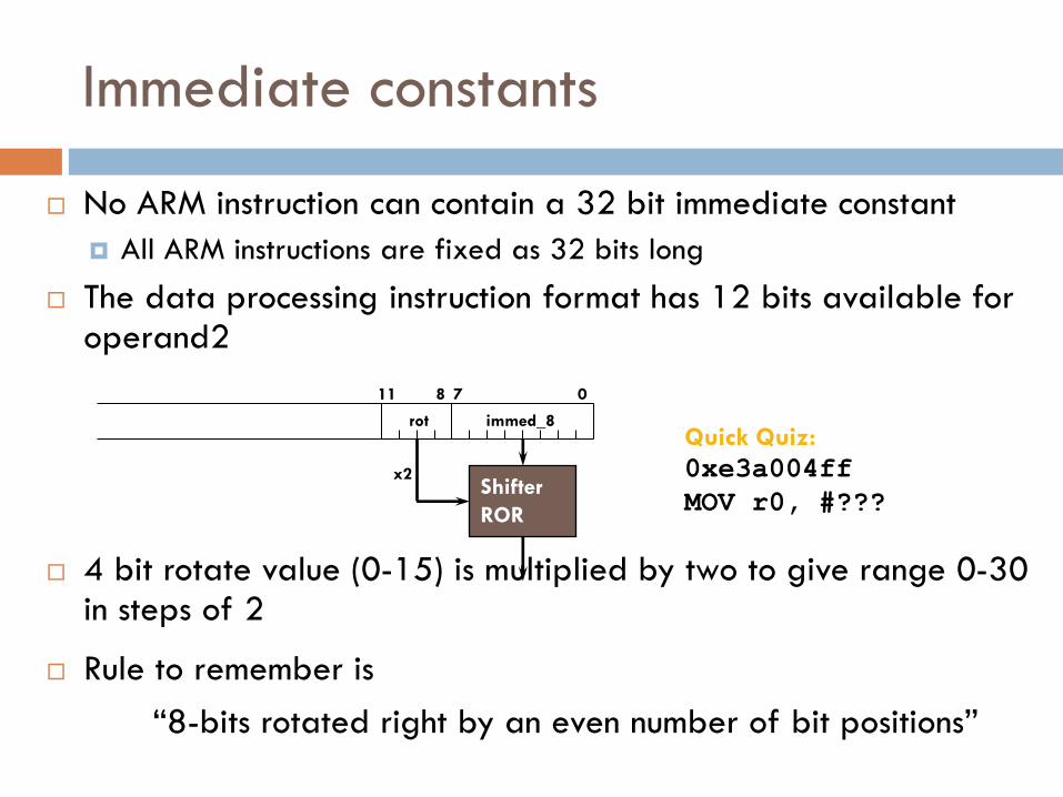
No ARM instruction can contain a 32 bit immediate constant
All ARM instructions are fixed as 32 bits long
The data processing instruction format has 12 bits available for operand2
4 bit rotate value (0-15) is multiplied by two to give range 0-30 in steps of 2
Rule to remember is
“8-bits rotated right by an even number of bit positions”
0 7 11 8
immed_8
Shifter
ROR
rot
x2
Quick Quiz:
0xe3a004ff
MOV r0, #???
Immediate constants
Data Processing Exercise
1. How would you load the two’s complement
representation of -1 into Register 3 using one
instruction?
2. Multiply a number by 35, guaranteeing that it
executes in 2 core clock cycles.
Data Processing Solutions
1. MOVN r6, #0
2. ADD r9,r8,r8,LSL #2 ; r9=r8*5
RSB r10,r9,r9,LSL #3 ; r10=r9*7
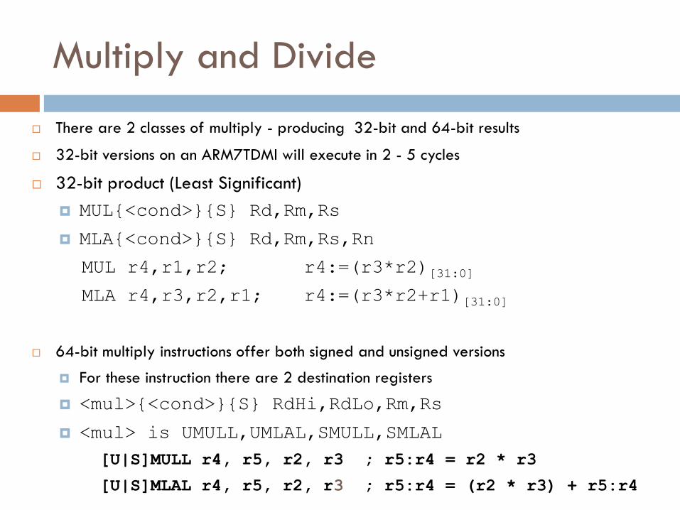
There are 2 classes of multiply - producing 32-bit and 64-bit results
32-bit versions on an ARM7TDMI will execute in 2 - 5 cycles
32-bit product (Least Significant)
MUL{<cond>}{S} Rd,Rm,Rs
MLA{<cond>}{S} Rd,Rm,Rs,Rn
MUL r4,r1,r2; r4:=(r3*r2)[31:0]
MLA r4,r3,r2,r1; r4:=(r3*r2+r1)[31:0]
64-bit multiply instructions offer both signed and unsigned versions
For these instruction there are 2 destination registers
<mul>{<cond>}{S} RdHi,RdLo,Rm,Rs
<mul> is UMULL,UMLAL,SMULL,SMLAL
[U|S]MULL r4, r5, r2, r3 ; r5:r4 = r2 * r3
[U|S]MLAL r4, r5, r2, r3 ; r5:r4 = (r2 * r3) + r5:r4
Multiply and Divide
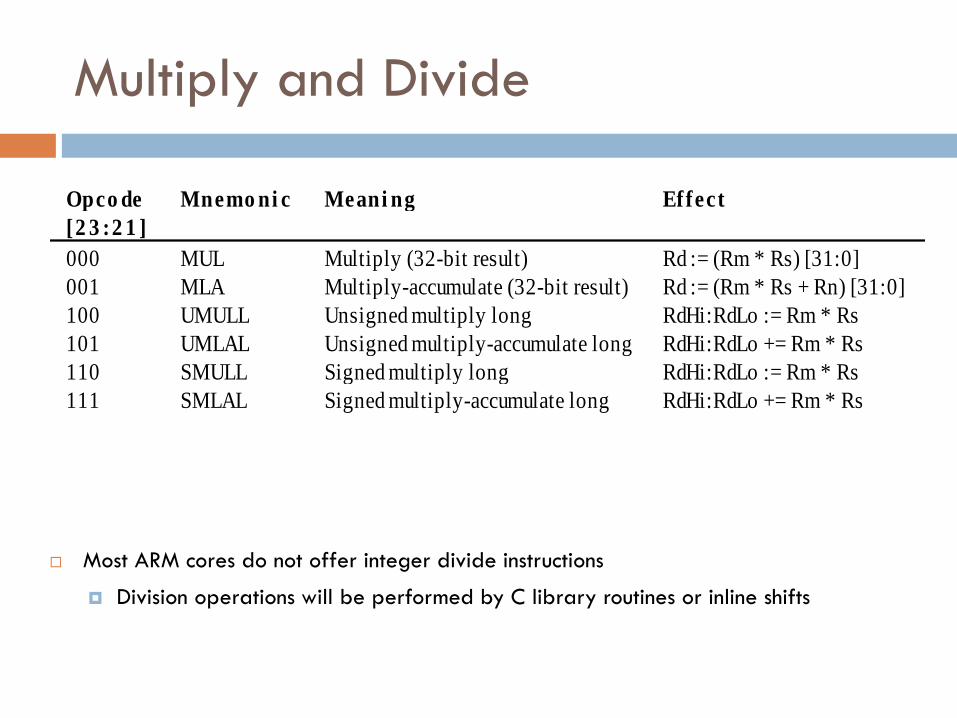
Multiply and Divide
Most ARM cores do not offer integer divide instructions
Division operations will be performed by C library routines or inline shifts
Opco de
[2 3 :2 1 ]
Mnemo ni c Meani ng Effect
000 MUL Multiply (32-bit result) Rd := (Rm * Rs) [31:0]
001 MLA Multiply-accumulate (32-bit result) Rd := (Rm * Rs + Rn) [31:0]
100 UMULL Unsigned multiply long RdHi:RdLo := Rm * Rs
101 UMLAL Unsigned multiply-accumulate long RdHi:RdLo += Rm * Rs
110 SMULL Signed multiply long RdHi:RdLo := Rm * Rs
111 SMLAL Signed multiply-accumulate long RdHi:RdLo += Rm * Rs
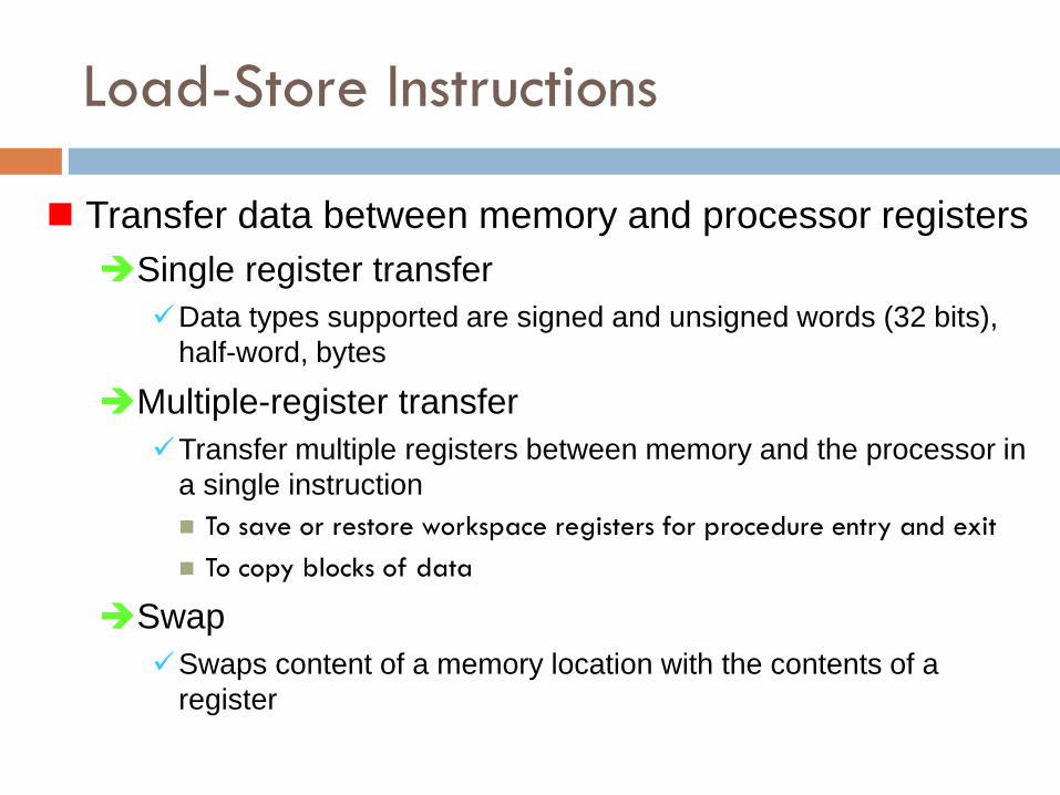
Load-Store Instructions
Transfer data between memory and processor registers
Single register transfer
Data types supported are signed and unsigned words (32 bits),
half-word, bytes
Multiple-register transfer
Transfer multiple registers between memory and the processor in
a single instruction
To save or restore workspace registers for procedure entry and exit
To copy blocks of data
Swap
Swaps content of a memory location with the contents of a
register
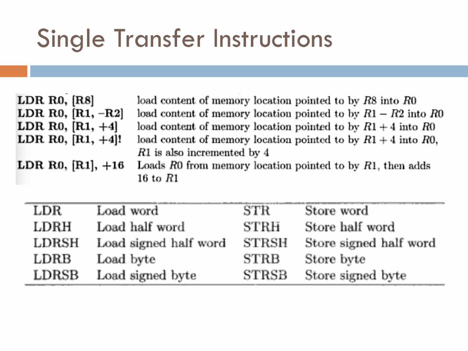
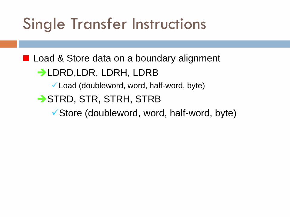
Single Transfer Instructions
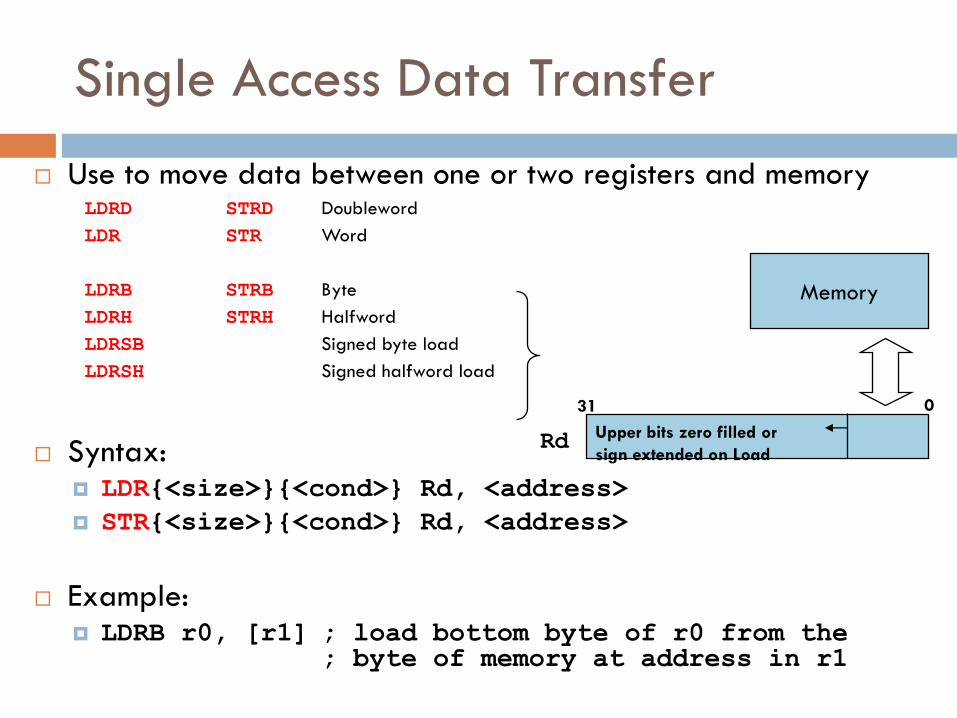
Single Access Data Transfer
Use to move data between one or two registers and memory LDRD STRD Doubleword
LDR STR Word
LDRB STRB Byte
LDRH STRH Halfword
LDRSB Signed byte load
LDRSH Signed halfword load
Syntax: LDR{<size>}{<cond>} Rd, <address>
STR{<size>}{<cond>} Rd, <address>
Example: LDRB r0, [r1] ; load bottom byte of r0 from the ; byte of memory at address in r1
Upper bits zero filled or
sign extended on Load
Memory
Rd
31 0
Single Transfer Instructions
Load & Store data on a boundary alignment
LDRD,LDR, LDRH, LDRB
Load (doubleword, word, half-word, byte)
STRD, STR, STRH, STRB
Store (doubleword, word, half-word, byte)
Single Transfer Instructions
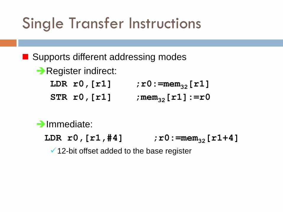
Supports different addressing modes
Register indirect:
LDR r0,[r1] ;r0:=mem32[r1]
STR r0,[r1] ;mem32[r1]:=r0
Immediate:
LDR r0,[r1,#4] ;r0:=mem32[r1+4]
12-bit offset added to the base register
Single Transfer Instructions
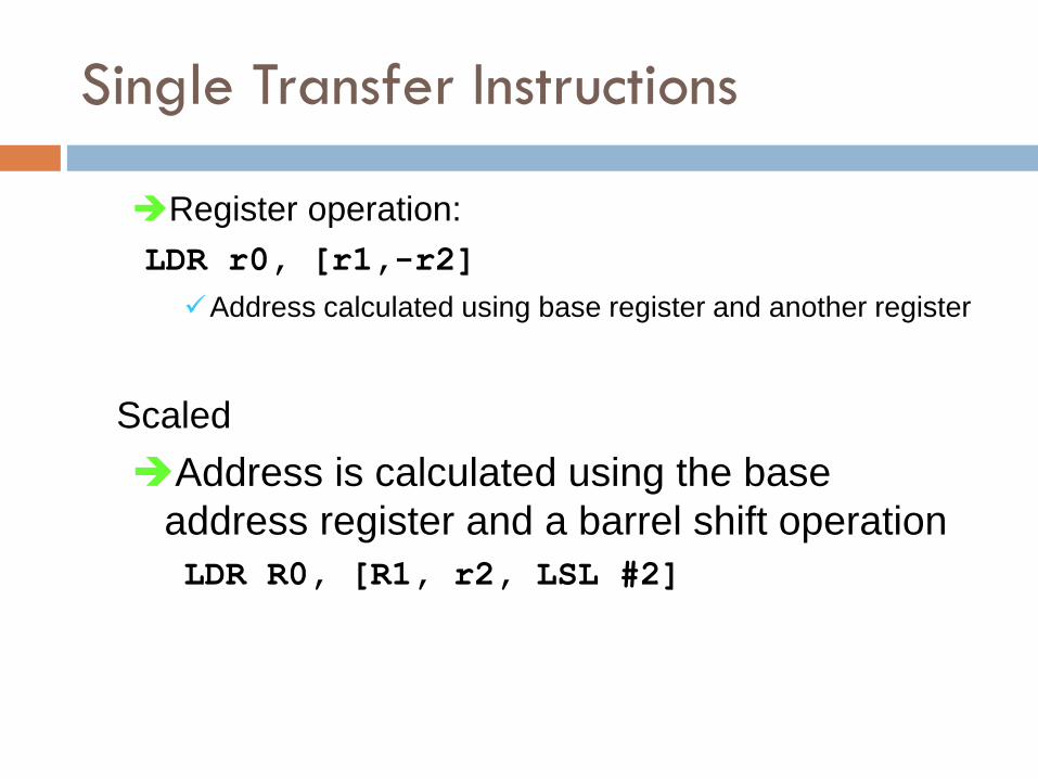
Register operation:
LDR r0, [r1,-r2]
Address calculated using base register and another register
Scaled
Address is calculated using the base
address register and a barrel shift operation
LDR R0, [R1, r2, LSL #2]
More Addressing Modes
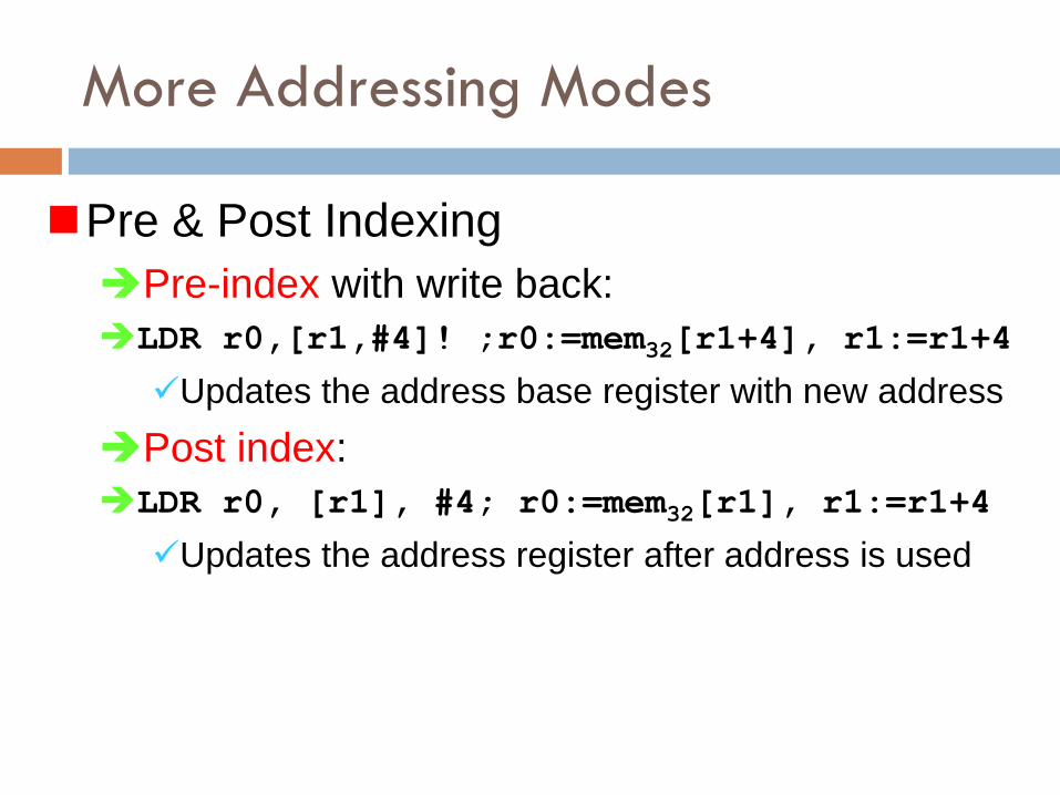
Pre & Post Indexing
Pre-index with write back:
LDR r0,[r1,#4]! ;r0:=mem32[r1+4], r1:=r1+4
Updates the address base register with new address
Post index:
LDR r0, [r1], #4; r0:=mem32[r1], r1:=r1+4
Updates the address register after address is used
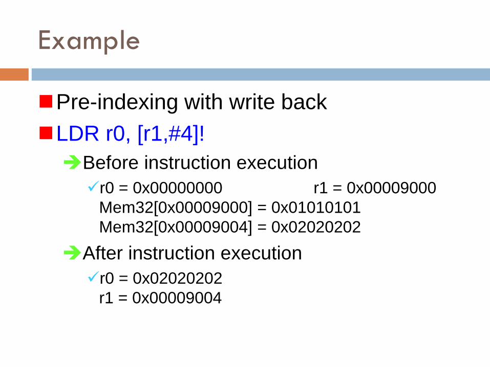
Example
Pre-indexing with write back
LDR r0, [r1,#4]!
Before instruction execution
r0 = 0x00000000 r1 = 0x00009000
Mem32[0x00009000] = 0x01010101
Mem32[0x00009004] = 0x02020202
After instruction execution
r0 = 0x02020202
r1 = 0x00009004
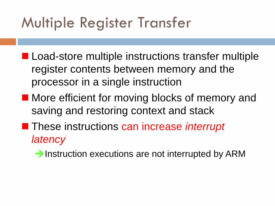
Multiple Register Transfer
Load-store multiple instructions transfer multiple
register contents between memory and the
processor in a single instruction
More efficient for moving blocks of memory and
saving and restoring context and stack
These instructions can increase interrupt
latency
Instruction executions are not interrupted by ARM
Multiple Byte Load-Store
Any subset of current bank of registers
can be transferred to memory or fetched
from memory
LDM
SDM
The base register Rn determines source
or destination address
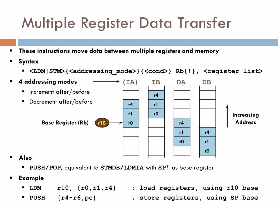
These instructions move data between multiple registers and memory
Syntax
<LDM|STM>{<addressing_mode>}{<cond>} Rb{!}, <register list>
4 addressing modes
Increment after/before
Decrement after/before
Also
PUSH/POP, equivalent to STMDB/LDMIA with SP! as base register
Example
LDM r10, {r0,r1,r4} ; load registers, using r10 base
PUSH {r4-r6,pc} ; store registers, using SP base
Multiple Register Data Transfer
(IA)
r1 Increasing
Address
r4
r0
r1
r4
r0
r1
r4
r0 r1
r4
r0
r10
IB DA DB
Base Register (Rb)
Example
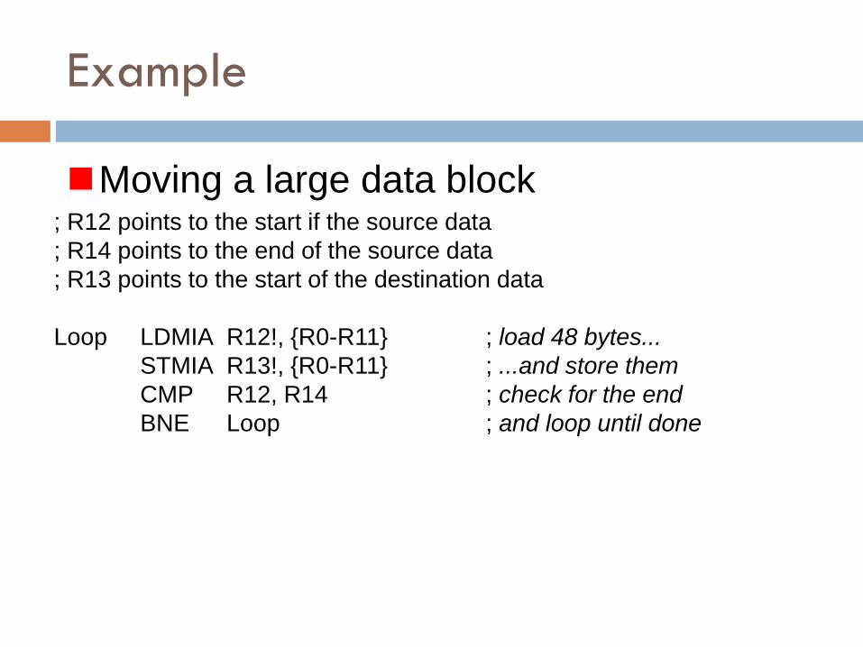
Moving a large data block ; R12 points to the start if the source data
; R14 points to the end of the source data
; R13 points to the start of the destination data
Loop LDMIA R12!, {R0-R11} ; load 48 bytes...
STMIA R13!, {R0-R11} ; ...and store them
CMP R12, R14 ; check for the end
BNE Loop ; and loop until done
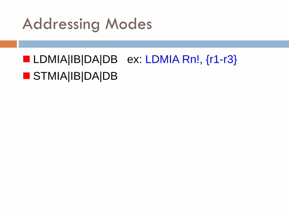
Addressing Modes
LDMIA|IB|DA|DB ex: LDMIA Rn!, {r1-r3}
STMIA|IB|DA|DB
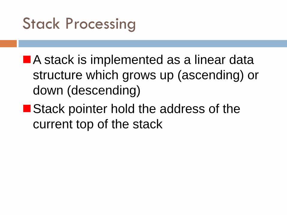
Stack Processing
A stack is implemented as a linear data
structure which grows up (ascending) or
down (descending)
Stack pointer hold the address of the
current top of the stack
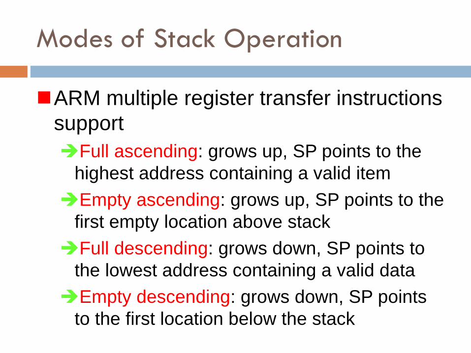
Modes of Stack Operation
ARM multiple register transfer instructions
support
Full ascending: grows up, SP points to the
highest address containing a valid item
Empty ascending: grows up, SP points to the
first empty location above stack
Full descending: grows down, SP points to
the lowest address containing a valid data
Empty descending: grows down, SP points
to the first location below the stack
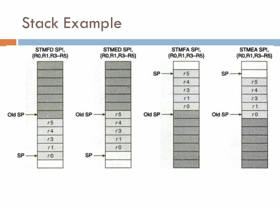
Stack Example
Some Stack Instructions
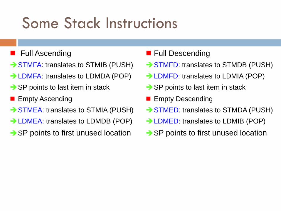
Full Ascending
STMFA: translates to STMIB (PUSH)
LDMFA: translates to LDMDA (POP)
SP points to last item in stack
Empty Ascending
STMEA: translates to STMIA (PUSH)
LDMEA: translates to LDMDB (POP)
SP points to first unused location
Full Descending
STMFD: translates to STMDB (PUSH)
LDMFD: translates to LDMIA (POP)
SP points to last item in stack
Empty Descending
STMED: translates to STMDA (PUSH)
LDMED: translates to LDMIB (POP)
SP points to first unused location
SWAP Instruction
Special case of load store instruction
Swap instructions SWP{<cond>}{B} Rd,Rm,[Rn]
Rd <- [Rn], [Rn] <- Rm
SWP: swap a word between memory and
register
SWPB: swap a byte between memory and
register
Useful for implementing synchronization
primitives like semaphore
Control Flow Instructions
Branch instructions
Conditional Branches
Conditional Execution
Branch and Link instructions
Subroutine Return instructions
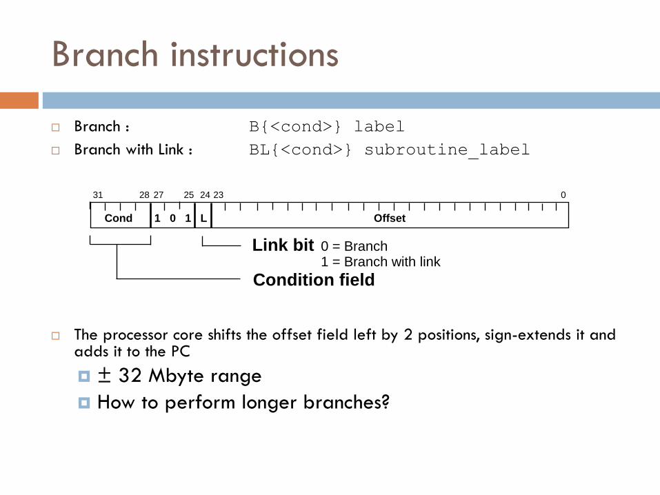
Branch : B{<cond>} label
Branch with Link : BL{<cond>} subroutine_label
The processor core shifts the offset field left by 2 positions, sign-extends it and adds it to the PC
± 32 Mbyte range
How to perform longer branches?
28 31 24 0
Cond 1 0 1 L Offset
Condition field
Link bit 0 = Branch 1 = Branch with link
23 25 27
Branch instructions
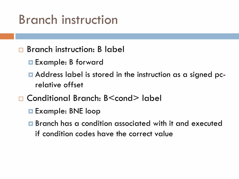
Branch instruction
Branch instruction: B label
Example: B forward
Address label is stored in the instruction as a signed pc-
relative offset
Conditional Branch: B<cond> label
Example: BNE loop
Branch has a condition associated with it and executed
if condition codes have the correct value
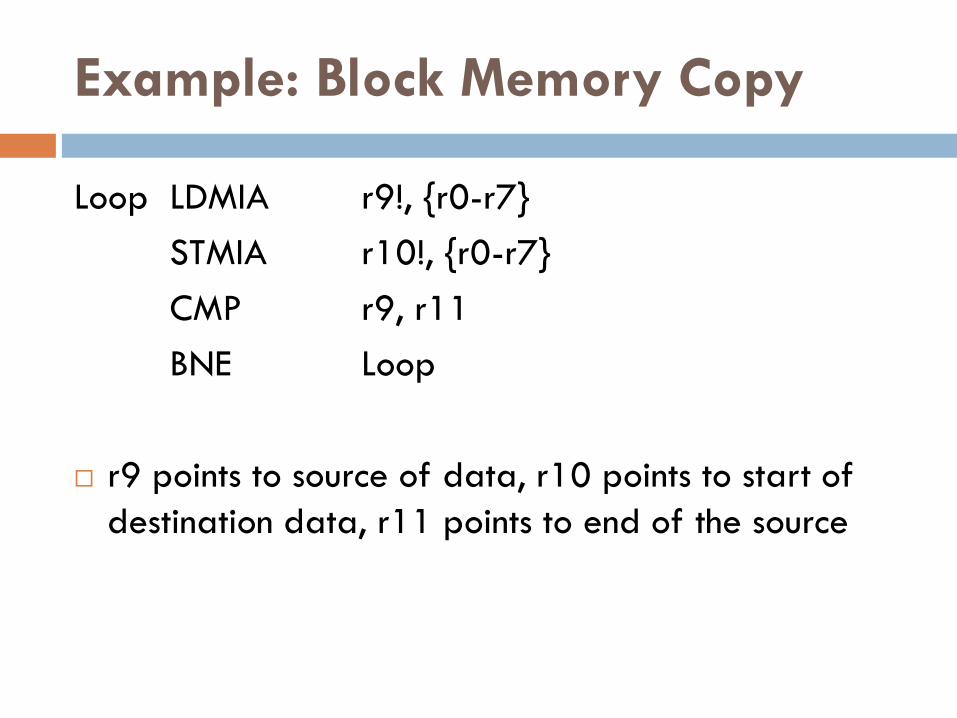
Example: Block Memory Copy
Loop LDMIA r9!, {r0-r7}
STMIA r10!, {r0-r7}
CMP r9, r11
BNE Loop
r9 points to source of data, r10 points to start of
destination data, r11 points to end of the source
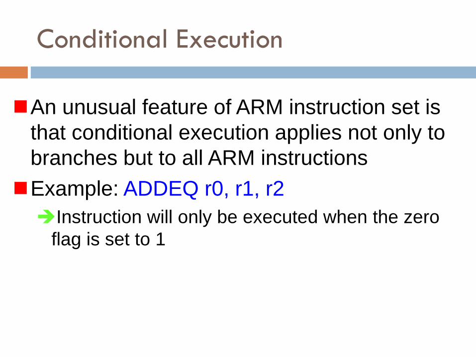
Conditional Execution
An unusual feature of ARM instruction set is
that conditional execution applies not only to
branches but to all ARM instructions
Example: ADDEQ r0, r1, r2
Instruction will only be executed when the zero
flag is set to 1
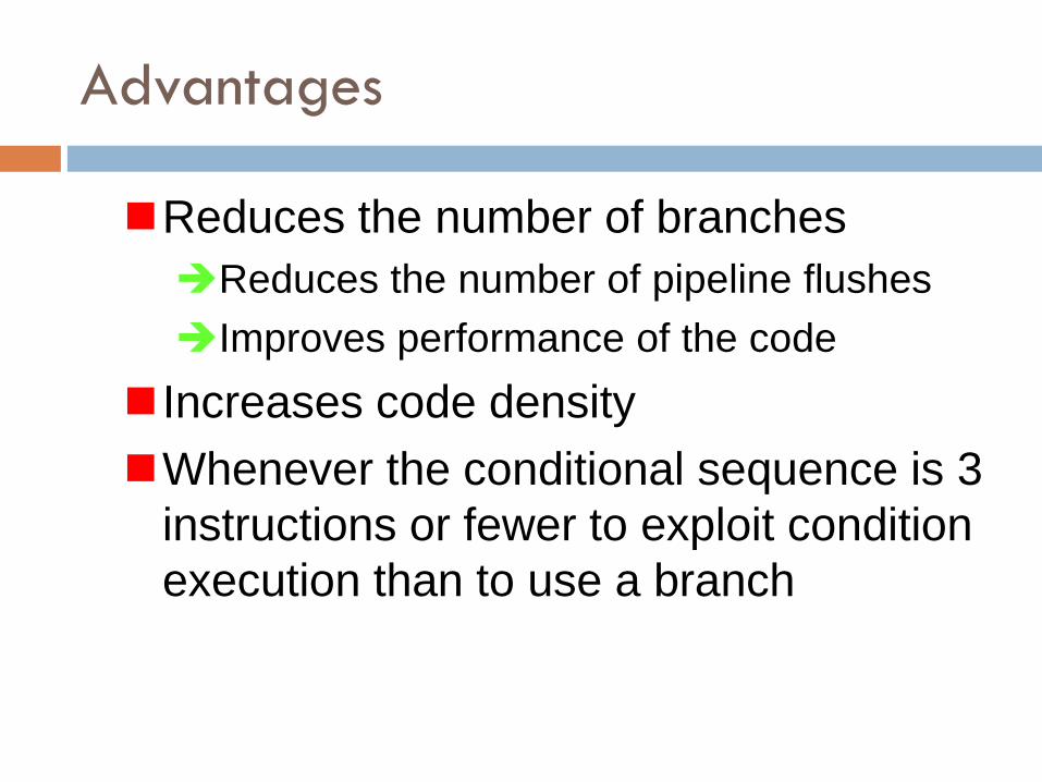
Advantages
Reduces the number of branches
Reduces the number of pipeline flushes
Improves performance of the code
Increases code density
Whenever the conditional sequence is 3
instructions or fewer to exploit condition
execution than to use a branch
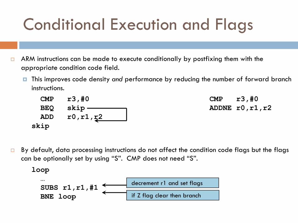
ARM instructions can be made to execute conditionally by postfixing them with the
appropriate condition code field.
This improves code density and performance by reducing the number of forward branch
instructions.
CMP r3,#0 CMP r3,#0
BEQ skip ADDNE r0,r1,r2
ADD r0,r1,r2
skip
By default, data processing instructions do not affect the condition code flags but the flags
can be optionally set by using “S”. CMP does not need “S”.
loop
…
SUBS r1,r1,#1
BNE loop
if Z flag clear then branch
decrement r1 and set flags
Conditional Execution and Flags
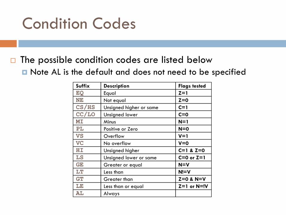
Condition Codes
Not equal
Unsigned higher or same
Unsigned lower
Minus
Equal
Overflow
No overflow
Unsigned higher
Unsigned lower or same
Positive or Zero
Less than
Greater than
Less than or equal
Always
Greater or equal
EQ
NE
CS/HS
CC/LO
PL
VS
HI
LS
GE
LT
GT
LE
AL
MI
VC
Suffix Description
Z=0
C=1
C=0
Z=1
Flags tested
N=1
N=0
V=1
V=0
C=1 & Z=0
C=0 or Z=1
N=V
N!=V
Z=0 & N=V
Z=1 or N=!V
The possible condition codes are listed below
Note AL is the default and does not need to be specified
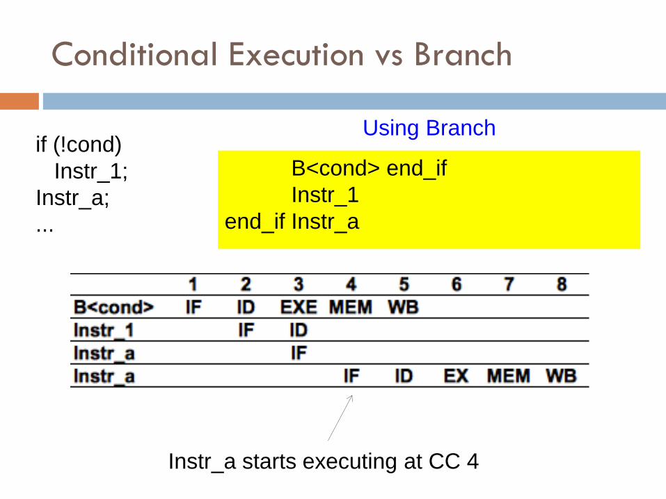
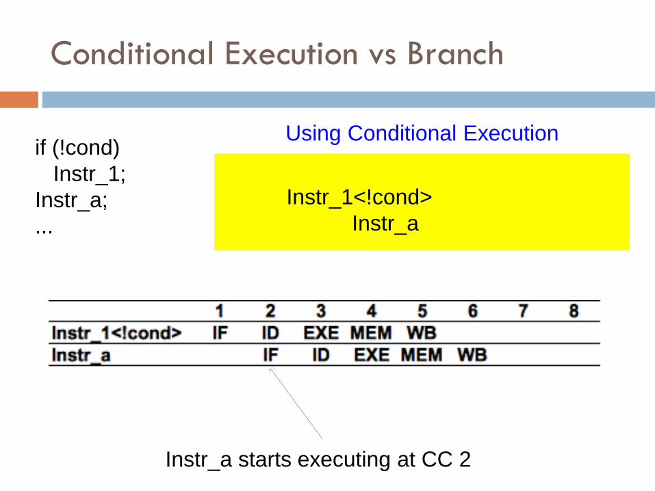
Conditional Execution vs Branch
if (!cond)
Instr_1;
Instr_a;
...
B<cond> end_if
Instr_1
end_if Instr_a
Using Branch
Instr_a starts executing at CC 4
Conditional Execution vs Branch
if (!cond)
Instr_1;
Instr_a;
...
Instr_1<!cond>
Instr_a
Using Conditional Execution
Instr_a starts executing at CC 2
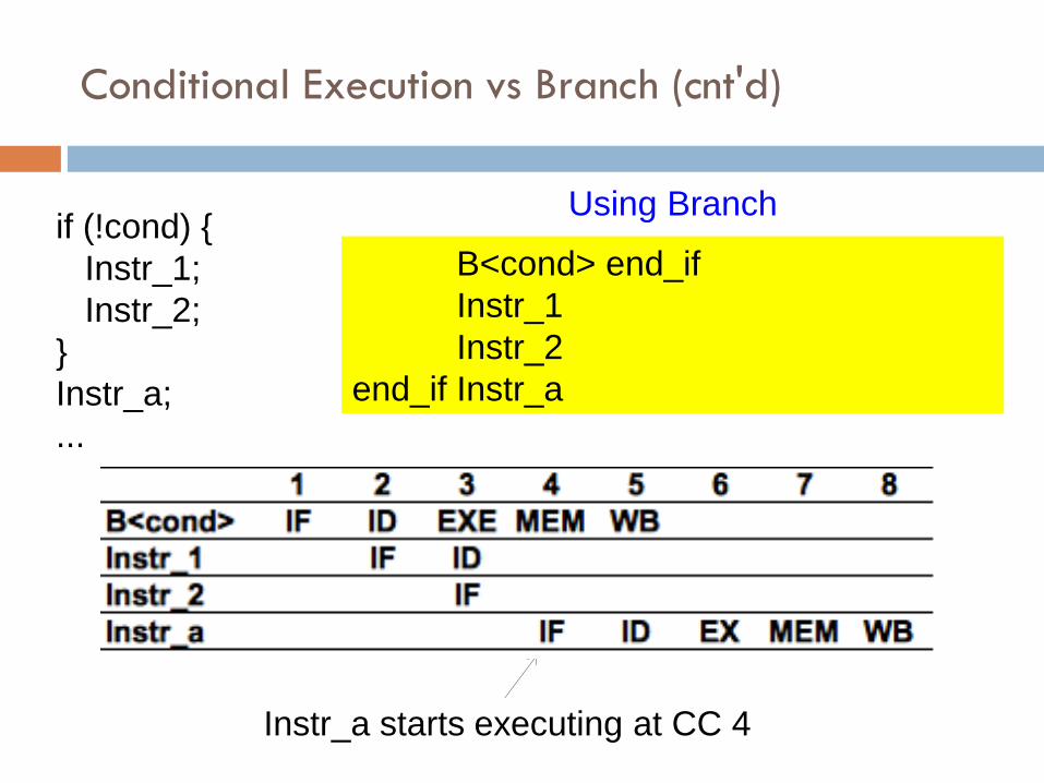
Conditional Execution vs Branch (cnt'd)
if (!cond) {
Instr_1;
Instr_2;
}
Instr_a;
...
B<cond> end_if
Instr_1
Instr_2
end_if Instr_a
Using Branch
Instr_a starts executing at CC 4
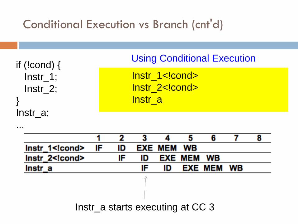
Conditional Execution vs Branch (cnt'd)
if (!cond) {
Instr_1;
Instr_2;
}
Instr_a;
...
Instr_1<!cond>
Instr_2<!cond>
Instr_a
Using Conditional Execution
Instr_a starts executing at CC 3
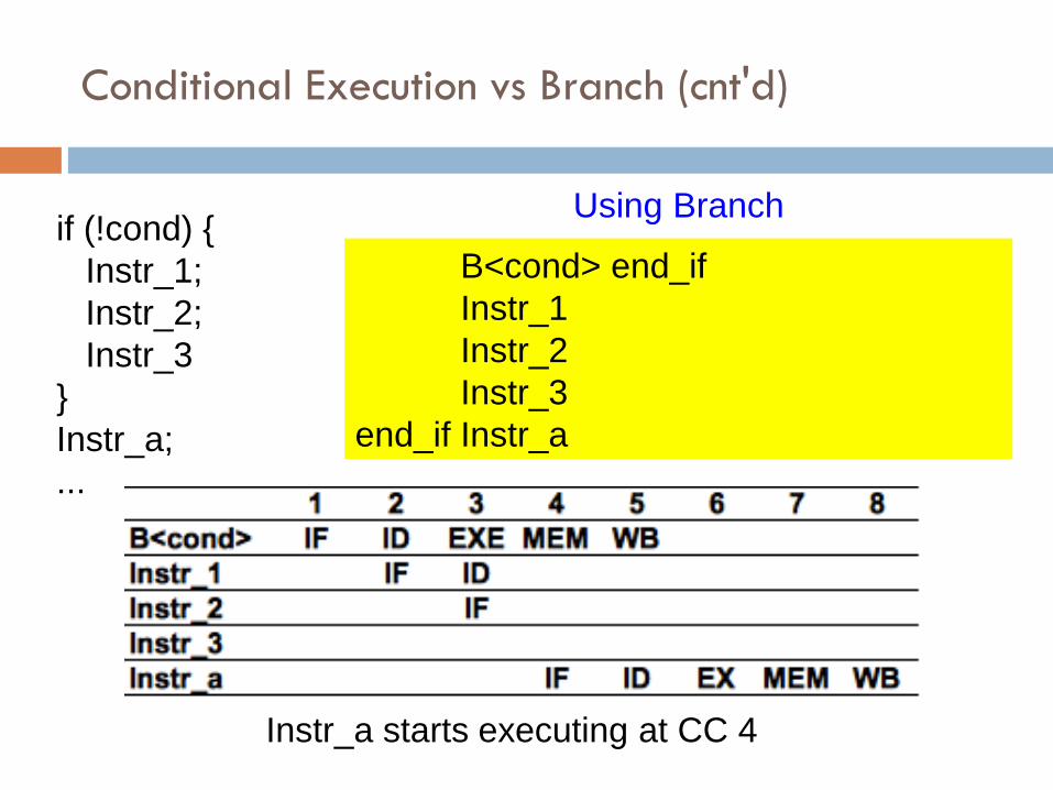
Conditional Execution vs Branch (cnt'd)
if (!cond) {
Instr_1;
Instr_2;
Instr_3
}
Instr_a;
...
B<cond> end_if
Instr_1
Instr_2
Instr_3
end_if Instr_a
Using Branch
Instr_a starts executing at CC 4
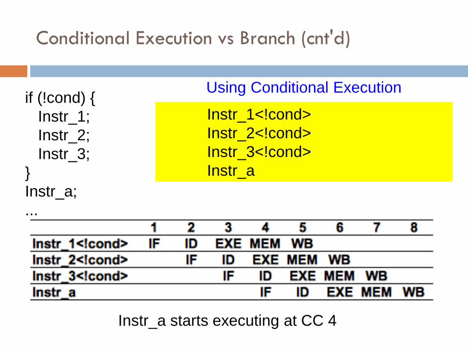
Conditional Execution vs Branch (cnt'd)
if (!cond) {
Instr_1;
Instr_2;
Instr_3;
}
Instr_a;
...
Instr_1<!cond>
Instr_2<!cond>
Instr_3<!cond>
Instr_a
Using Conditional Execution
Instr_a starts executing at CC 4
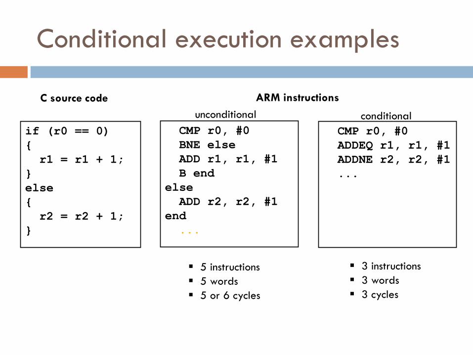
Conditional execution examples
if (r0 == 0)
{
r1 = r1 + 1;
}
else
{
r2 = r2 + 1;
}
C source code
5 instructions
5 words
5 or 6 cycles
3 instructions
3 words
3 cycles
CMP r0, #0
BNE else
ADD r1, r1, #1
B end
else
ADD r2, r2, #1
end
...
ARM instructions
unconditional
CMP r0, #0
ADDEQ r1, r1, #1
ADDNE r2, r2, #1
...
conditional
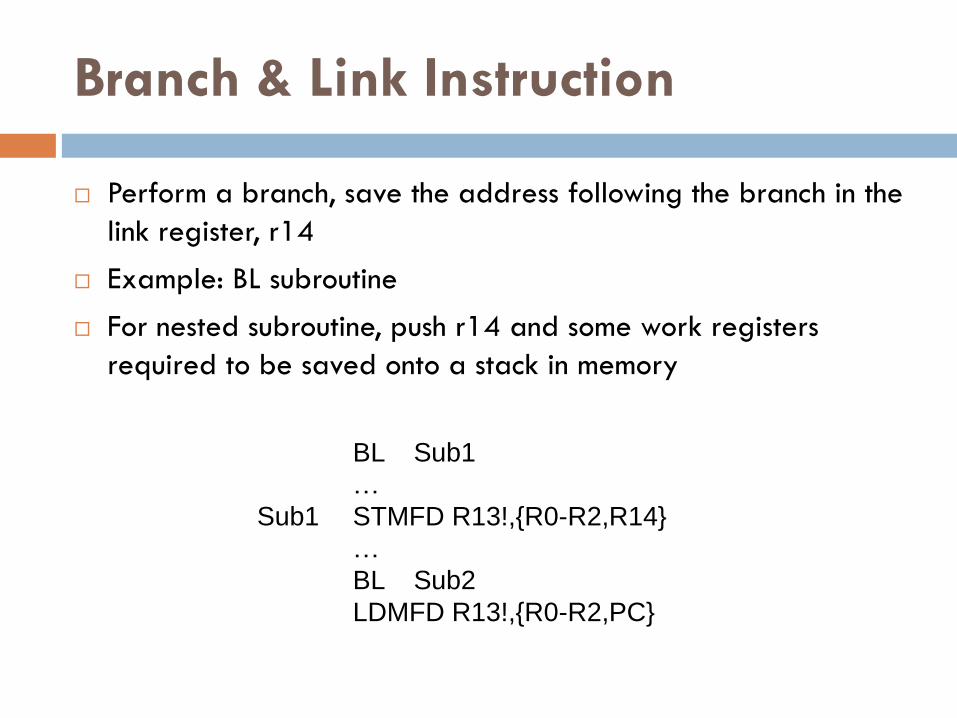
Branch & Link Instruction
Perform a branch, save the address following the branch in the
link register, r14
Example: BL subroutine
For nested subroutine, push r14 and some work registers
required to be saved onto a stack in memory
BL Sub1
…
Sub1 STMFD R13!,{R0-R2,R14}
…
BL Sub2
LDMFD R13!,{R0-R2,PC}
:
BL func2
:
:
BX lr
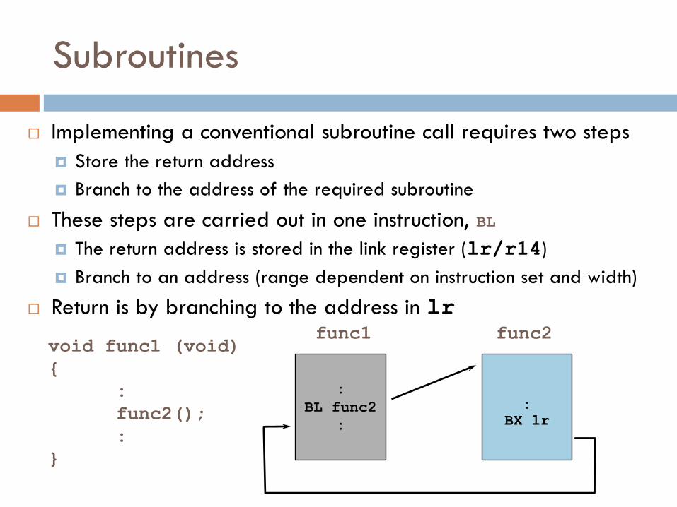
func1 func2 void func1 (void)
{
:
func2();
:
}
Subroutines
Implementing a conventional subroutine call requires two steps
Store the return address
Branch to the address of the required subroutine
These steps are carried out in one instruction, BL
The return address is stored in the link register (lr/r14)
Branch to an address (range dependent on instruction set and width)
Return is by branching to the address in lr
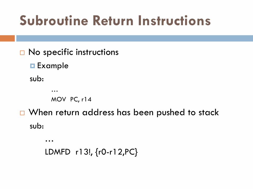
Subroutine Return Instructions
No specific instructions
Example
sub:
…
MOV PC, r14
When return address has been pushed to stack
sub:
…
LDMFD r13!, {r0-r12,PC}
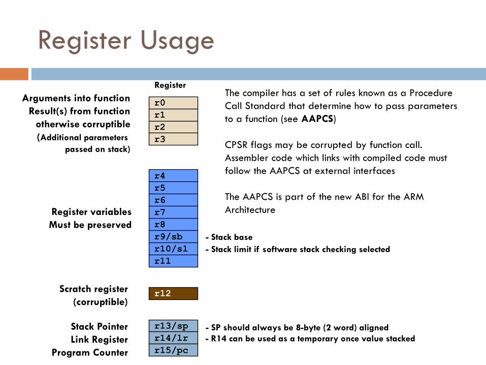
Register Usage
r8
r9/sb
r10/sl
r11
r12
r13/sp
r14/lr
r15/pc
r0
r1
r2
r3
r4
r5
r6
r7 Register variables
Must be preserved
Arguments into function
Result(s) from function
otherwise corruptible
(Additional parameters
passed on stack)
Scratch register
(corruptible)
Stack Pointer
Link Register
Program Counter
The compiler has a set of rules known as a Procedure
Call Standard that determine how to pass parameters
to a function (see AAPCS)
CPSR flags may be corrupted by function call.
Assembler code which links with compiled code must
follow the AAPCS at external interfaces
The AAPCS is part of the new ABI for the ARM
Architecture
Register
- Stack base
- Stack limit if software stack checking selected
- R14 can be used as a temporary once value stacked
- SP should always be 8-byte (2 word) aligned
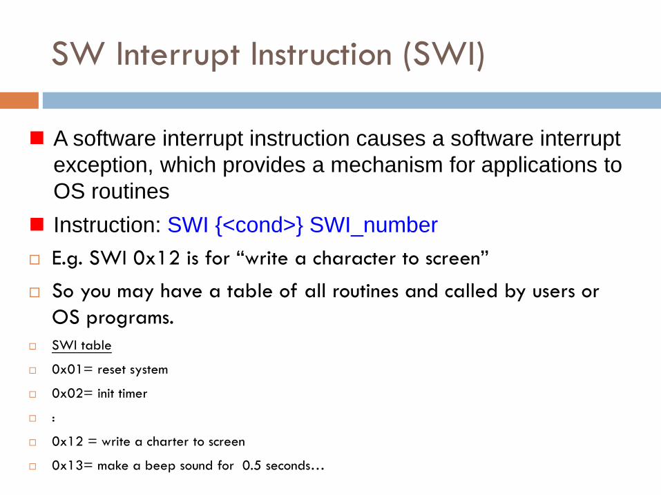
SW Interrupt Instruction (SWI)
A software interrupt instruction causes a software interrupt
exception, which provides a mechanism for applications to
OS routines
Instruction: SWI {<cond>} SWI_number
E.g. SWI 0x12 is for “write a character to screen”
So you may have a table of all routines and called by users or
OS programs.
SWI table
0x01= reset system
0x02= init timer
:
0x12 = write a charter to screen
0x13= make a beep sound for 0.5 seconds…
SWI
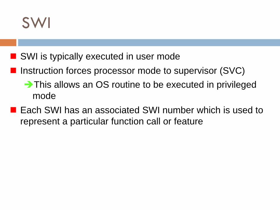
SWI is typically executed in user mode
Instruction forces processor mode to supervisor (SVC)
This allows an OS routine to be executed in privileged
mode
Each SWI has an associated SWI number which is used to
represent a particular function call or feature
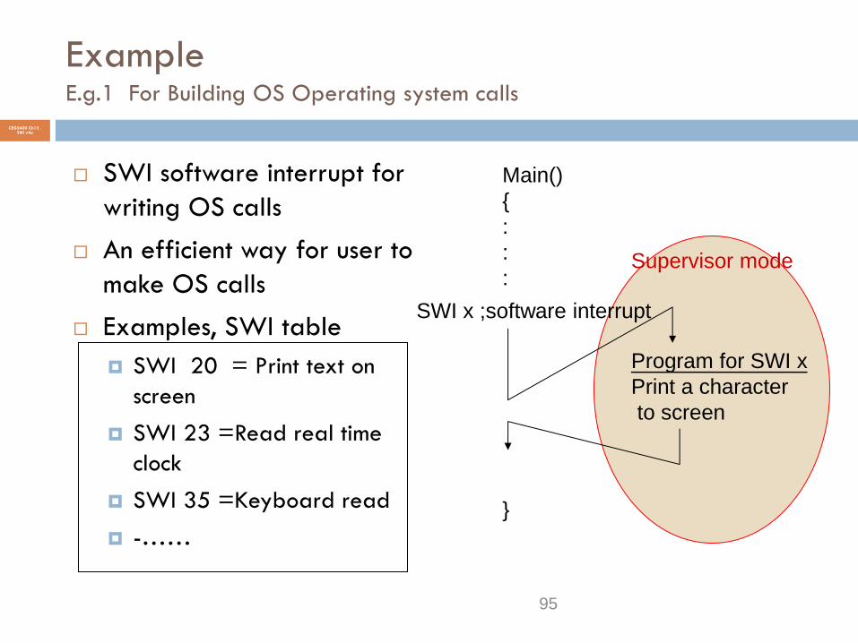
Example E.g.1 For Building OS Operating system calls
SWI software interrupt for
writing OS calls
An efficient way for user to
make OS calls
Examples, SWI table
SWI 20 = Print text on
screen
SWI 23 =Read real time
clock
SWI 35 =Keyboard read
-……
CEG2400 Ch12 . SWI v4a
95
Main()
{
:
:
:
}
Program for SWI x
Print a character
to screen
SWI x ;software interrupt
Supervisor mode
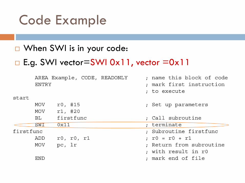
Code Example
When SWI is in your code:
E.g. SWI vector=SWI 0x11, vector =0x11
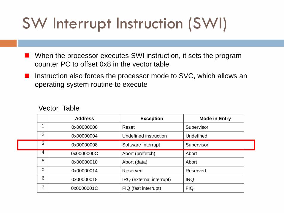
SW Interrupt Instruction (SWI)
When the processor executes SWI instruction, it sets the program
counter PC to offset 0x8 in the vector table
Instruction also forces the processor mode to SVC, which allows an
operating system routine to execute
Address Exception Mode in Entry
1 0x00000000 Reset Supervisor
2 0x00000004 Undefined instruction Undefined
3 0x00000008 Software Interrupt Supervisor
4 0x0000000C Abort (prefetch) Abort
5 0x00000010 Abort (data) Abort
x 0x00000014 Reserved Reserved
6 0x00000018 IRQ (external interrupt) IRQ
7 0x0000001C FIQ (fast interrupt) FIQ
Vector Table
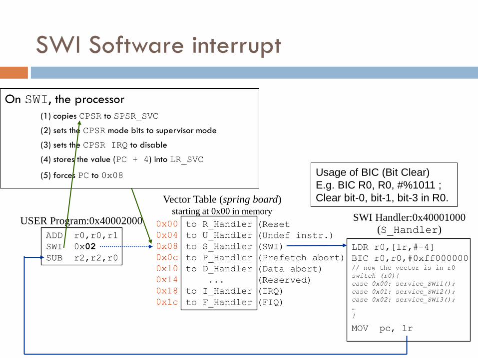
SWI Software interrupt
On SWI, the processor
(1) copies CPSR to SPSR_SVC
(2) sets the CPSR mode bits to supervisor mode
(3) sets the CPSR IRQ to disable
(4) stores the value (PC + 4) into LR_SVC
(5) forces PC to 0x08
ADD r0,r0,r1
SWI 0x02
SUB r2,r2,r0
USER Program:0x40002000 to R_Handler
to U_Handler
to S_Handler
to P_Handler
to D_Handler
...
to I_Handler
to F_Handler
Vector Table (spring board) starting at 0x00 in memory
0x00
0x04
0x08
0x0c
0x10
0x14
0x18
0x1c
(Reset
(Undef instr.)
(SWI)
(Prefetch abort)
(Data abort)
(Reserved)
(IRQ)
(FIQ)
LDR r0,[lr,#-4]
BIC r0,r0,#0xff000000 // now the vector is in r0
switch (r0){
case 0x00: service_SWI1();
case 0x01: service_SWI2();
case 0x02: service_SWI3();
…
}
MOV pc, lr
SWI Handler:0x40001000
(S_Handler)
Usage of BIC (Bit Clear)
E.g. BIC R0, R0, #%1011 ;
Clear bit-0, bit-1, bit-3 in R0.
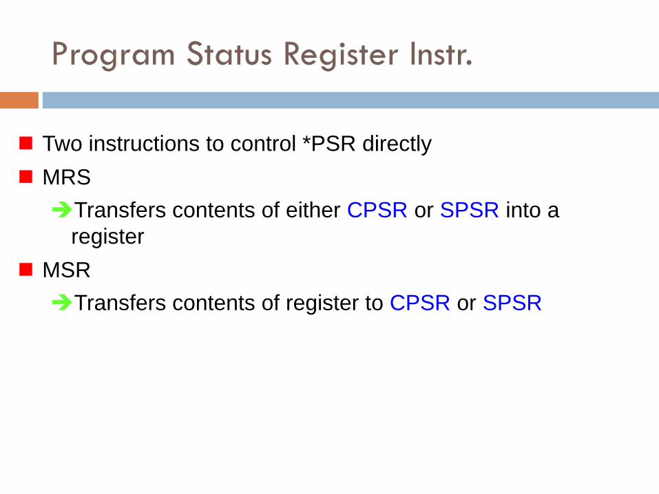
Program Status Register Instr.
Two instructions to control *PSR directly
MRS
Transfers contents of either CPSR or SPSR into a
register
MSR
Transfers contents of register to CPSR or SPSR
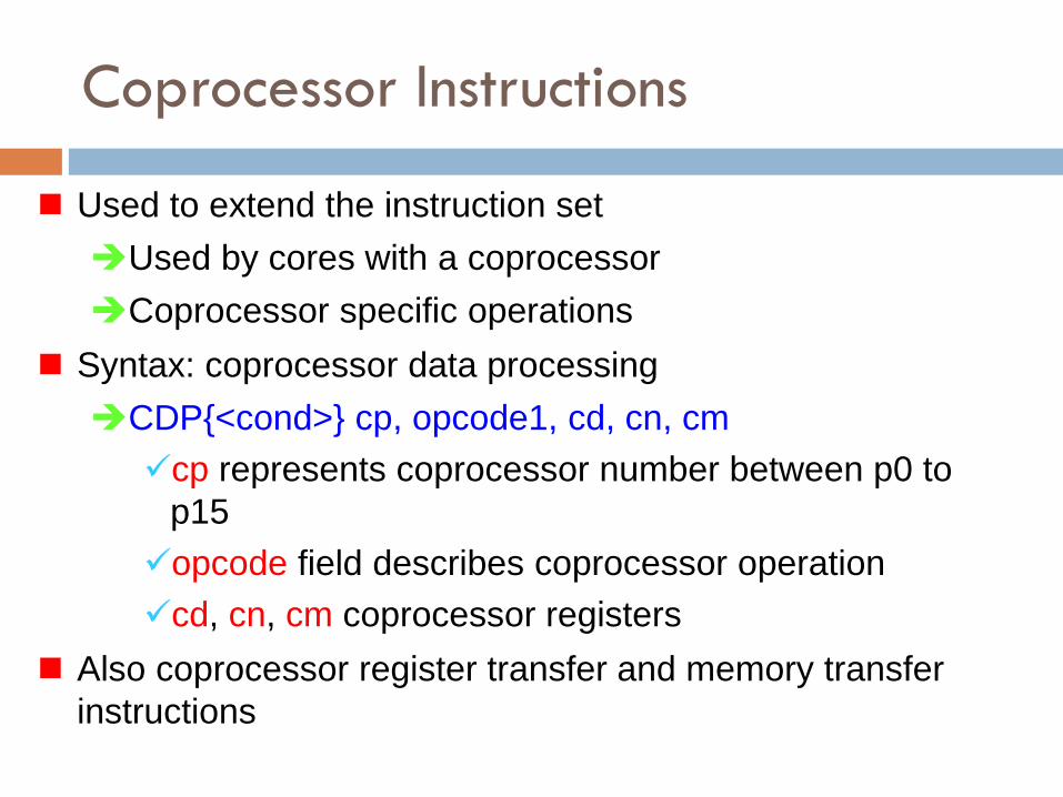
Coprocessor Instructions
Used to extend the instruction set
Used by cores with a coprocessor
Coprocessor specific operations
Syntax: coprocessor data processing
CDP{<cond>} cp, opcode1, cd, cn, cm
cp represents coprocessor number between p0 to
p15
opcode field describes coprocessor operation
cd, cn, cm coprocessor registers
Also coprocessor register transfer and memory transfer
instructions
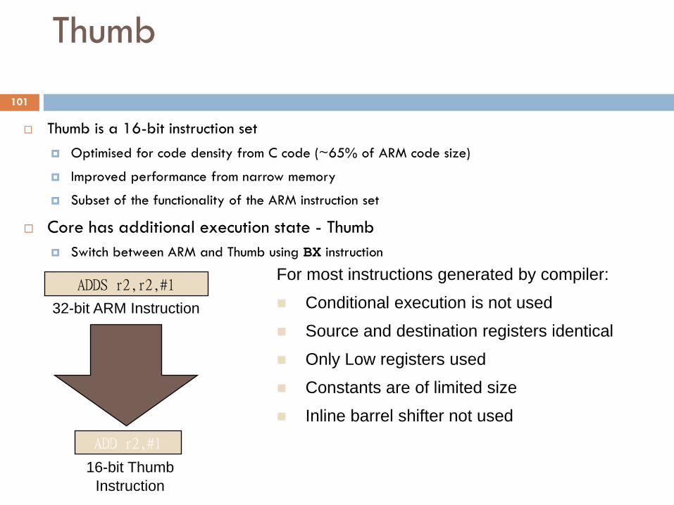
Thumb is a 16-bit instruction set
Optimised for code density from C code (~65% of ARM code size)
Improved performance from narrow memory
Subset of the functionality of the ARM instruction set
Core has additional execution state - Thumb
Switch between ARM and Thumb using BX instruction
0 1
5
31 0 ADDS r2,r2,#1
ADD r2,#1
32-bit ARM Instruction
16-bit Thumb
Instruction
For most instructions generated by compiler:
Conditional execution is not used
Source and destination registers identical
Only Low registers used
Constants are of limited size
Inline barrel shifter not used
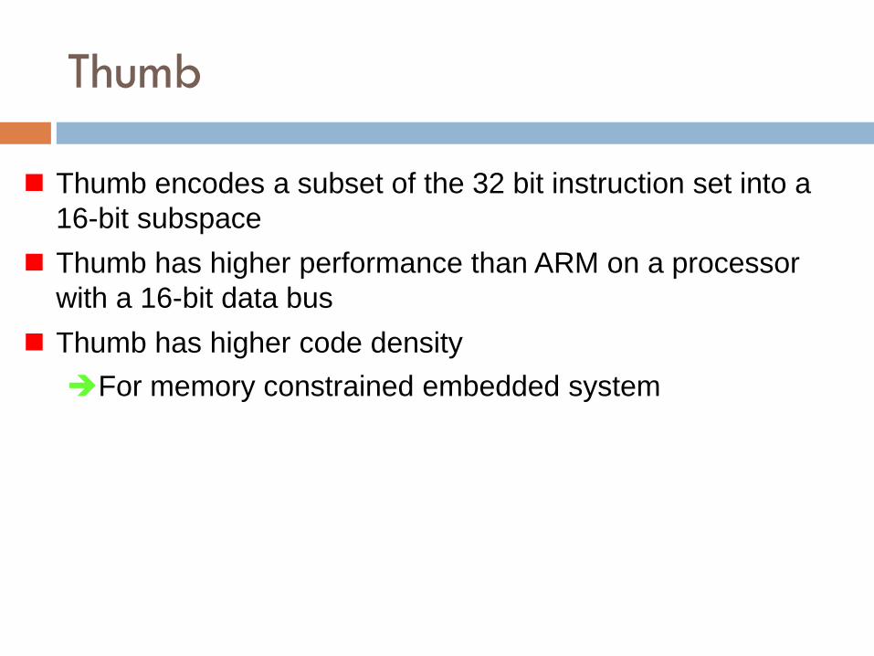
Thumb
101
Thumb
Thumb encodes a subset of the 32 bit instruction set into a
16-bit subspace
Thumb has higher performance than ARM on a processor
with a 16-bit data bus
Thumb has higher code density
For memory constrained embedded system
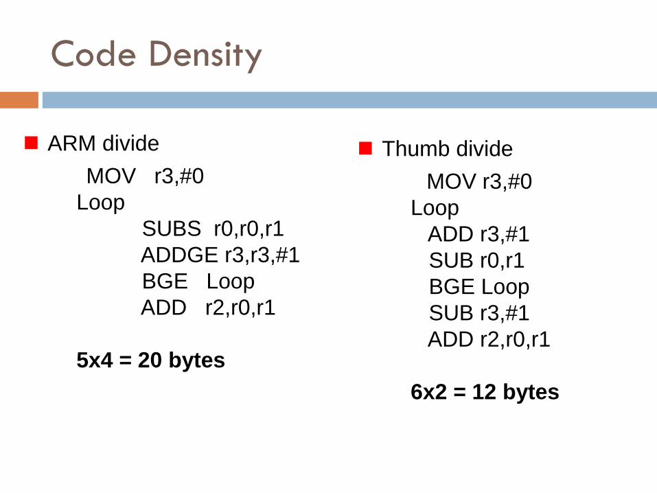
Code Density
ARM divide
MOV r3,#0
Loop
SUBS r0,r0,r1
ADDGE r3,r3,#1
BGE Loop
ADD r2,r0,r1
5x4 = 20 bytes
Thumb divide
MOV r3,#0
Loop
ADD r3,#1
SUB r0,r1
BGE Loop
SUB r3,#1
ADD r2,r0,r1
6x2 = 12 bytes
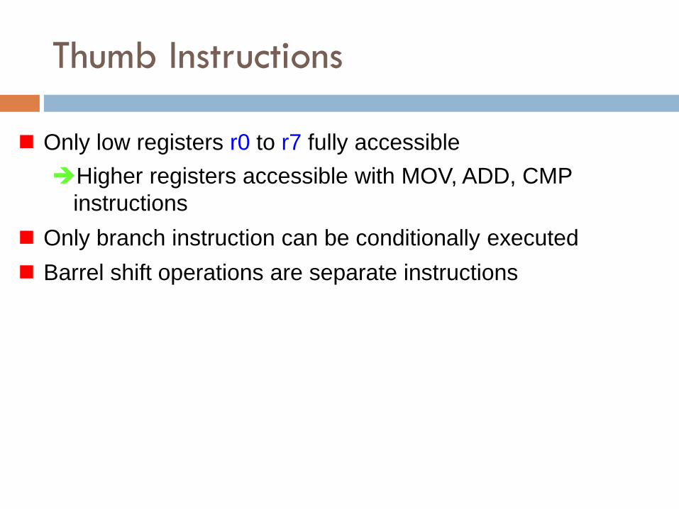
Thumb Instructions
Only low registers r0 to r7 fully accessible
Higher registers accessible with MOV, ADD, CMP
instructions
Only branch instruction can be conditionally executed
Barrel shift operations are separate instructions
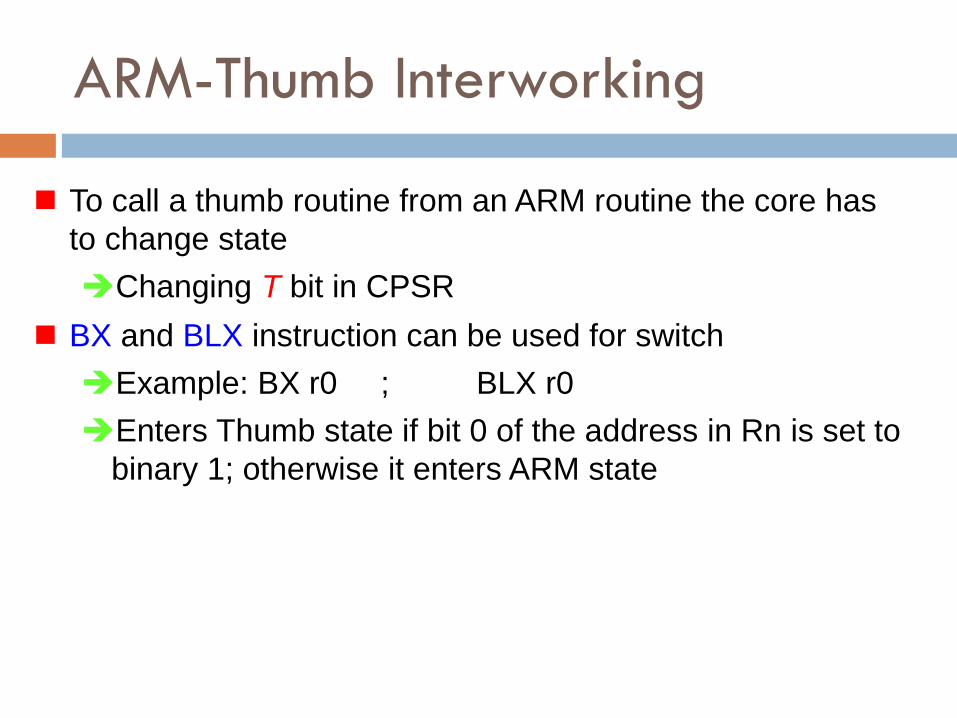
ARM-Thumb Interworking
To call a thumb routine from an ARM routine the core has
to change state
Changing T bit in CPSR
BX and BLX instruction can be used for switch
Example: BX r0 ; BLX r0
Enters Thumb state if bit 0 of the address in Rn is set to
binary 1; otherwise it enters ARM state
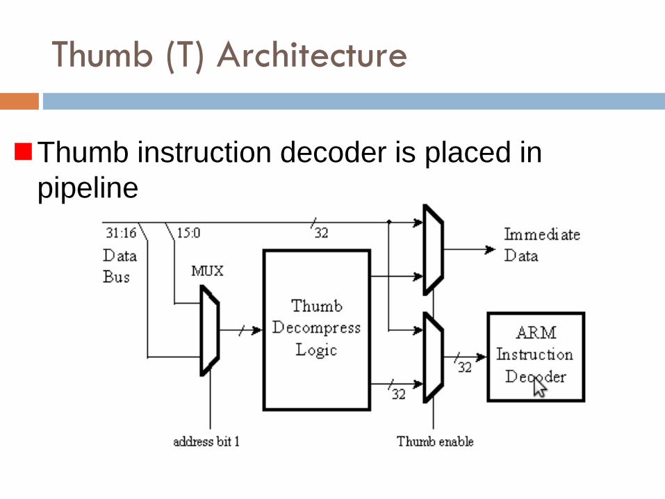
Thumb (T) Architecture
Thumb instruction decoder is placed in
pipeline
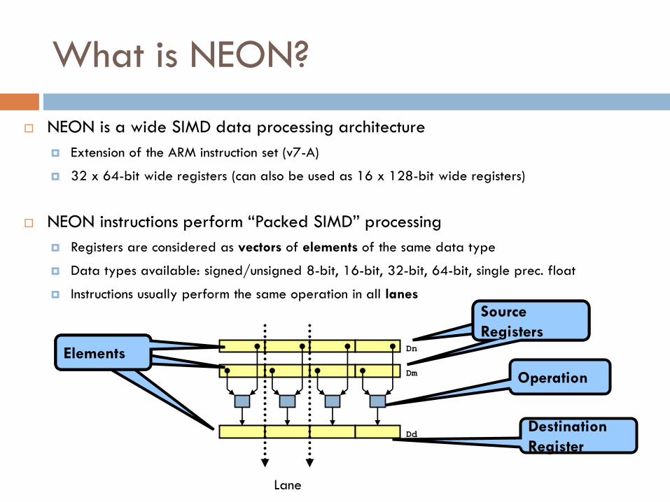
What is NEON?
NEON is a wide SIMD data processing architecture
Extension of the ARM instruction set (v7-A)
32 x 64-bit wide registers (can also be used as 16 x 128-bit wide registers)
NEON instructions perform “Packed SIMD” processing
Registers are considered as vectors of elements of the same data type
Data types available: signed/unsigned 8-bit, 16-bit, 32-bit, 64-bit, single prec. float
Instructions usually perform the same operation in all lanes
Dn
Dm
Dd
Lane
Source
Registers
Source
Registers
Operation
Destination
Register
Elements Elements Elements
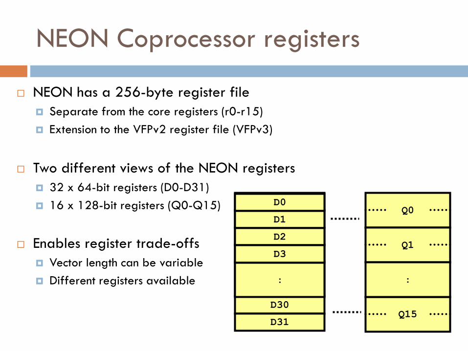
NEON Coprocessor registers
NEON has a 256-byte register file
Separate from the core registers (r0-r15)
Extension to the VFPv2 register file (VFPv3)
Two different views of the NEON registers
32 x 64-bit registers (D0-D31)
16 x 128-bit registers (Q0-Q15)
Enables register trade-offs
Vector length can be variable
Different registers available
Q0
Q1
Q15
:
D0
D1
D2
D3
:
D30
D31
D0
D1
D2
D3
:
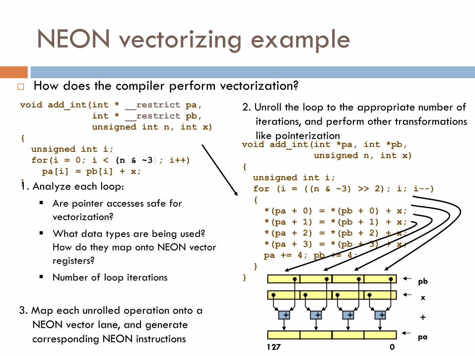
NEON vectorizing example
How does the compiler perform vectorization?
void add_int(int * __restrict pa,
int * __restrict pb,
unsigned int n, int x)
{
unsigned int i;
for(i = 0; i < (n & ~3); i++)
pa[i] = pb[i] + x;
} 1. Analyze each loop:
Are pointer accesses safe for
vectorization?
What data types are being used?
How do they map onto NEON vector
registers?
Number of loop iterations
void add_int(int *pa, int *pb,
unsigned n, int x)
{
unsigned int i;
for (i = ((n & ~3) >> 2); i; i--)
{
*(pa + 0) = *(pb + 0) + x;
*(pa + 1) = *(pb + 1) + x;
*(pa + 2) = *(pb + 2) + x;
*(pa + 3) = *(pb + 3) + x;
pa += 4; pb += 4;
}
}
2. Unroll the loop to the appropriate number of
iterations, and perform other transformations
like pointerization
3. Map each unrolled operation onto a
NEON vector lane, and generate
corresponding NEON instructions
+ + + +
pb
x
pa
+
0 127