Embed Size (px)
Citation preview
1ArrAyed WAveguide grAtingWhite Paper SEP 2019
Dr. Bernard Lee, Ryo Konno, Mac Watanabe
Arrayed Waveguide Grating

2ArrAyed WAveguide grAting

3ArrAyed WAveguide grAting
Contents
Arrayed Waveguide Grating
4
5
7
9
10
11
12
12
Introduction
Operation Principle and Device Characteristics
Different AWG Technologies
Applications
Mobile Fronthaul Network
Summary
Reference
Biography
4ArrAyed WAveguide grAting
Introduction
Arrayed Waveguide Gratings (AWG) are optical
planar devices that are usually used as multiplexers/
demultiplexers. These design of these devices are based on an array of
waveguides with both imaging and dispersive properties. Although
AWGs are also known under different names such as Phased Arrays
(PHASARs), and Waveguide Grating Routers (WRGs), AWG is the most
frequently used term in the telecommunications industry.
Light waves of different wavelengths interfere linearly with each other,
thus multiple optical channels with slightly different wavelengths
can be transmitted over a single optical fiber with minimal crosstalk
between the channels. Based on this principle, AWGs can be used
to multiplex multiple channels of different wavelengths on a single
optical fiber at the transmitter and also be used to demultiplex them
back into their individual channels of different wavelengths at the
receiver.
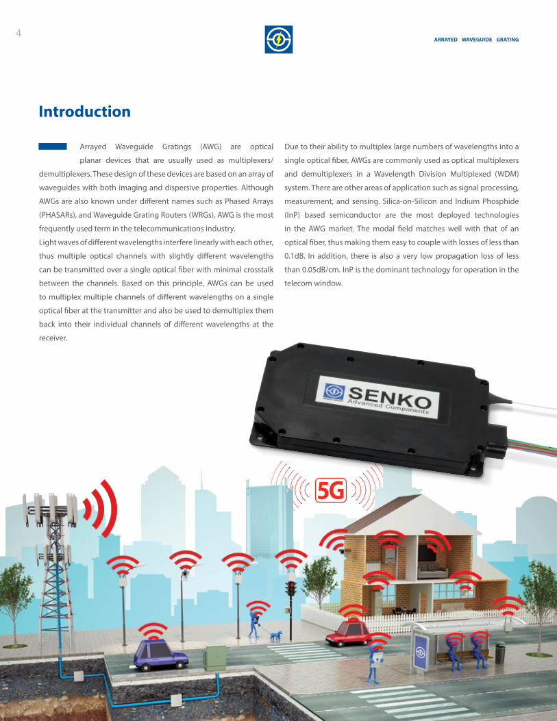
Due to their ability to multiplex large numbers of wavelengths into a
single optical fiber, AWGs are commonly used as optical multiplexers
and demultiplexers in a Wavelength Division Multiplexed (WDM)
system. There are other areas of application such as signal processing,
measurement, and sensing. Silica-on-Silicon and Indium Phosphide
(InP) based semiconductor are the most deployed technologies
in the AWG market. The modal field matches well with that of an
optical fiber, thus making them easy to couple with losses of less than
0.1dB. In addition, there is also a very low propagation loss of less
than 0.05dB/cm. InP is the dominant technology for operation in the
telecom window.
5ArrAyed WAveguide grAting
Arrayed Waveguides
Input Fiber Free Propagation Region(FPR)
Output Fiber
Operation Principle and Device Characteristics
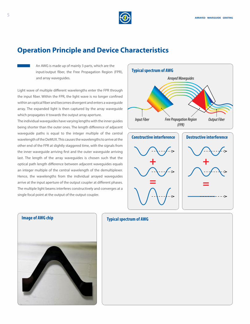
An AWG is made up of mainly 3 parts, which are the
input/output fiber, the Free Propagation Region (FPR),
and array waveguides.
Light wave of multiple different wavelengths enter the FPR through
the input fiber. Within the FPR, the light wave is no longer confined
within an optical fiber and becomes divergent and enters a waveguide
array. The expanded light is then captured by the array waveguide
which propagates it towards the output array aperture.
The individual waveguides have varying lengths with the inner guides
being shorter than the outer ones. The length difference of adjacent
waveguide paths is equal to the integer multiple of the central
wavelength of the DeMUX. This causes the wavelengths to arrive at the
other end of the FPR at slightly staggered time, with the signals from
the inner waveguide arriving first and the outer waveguide arriving
last. The length of the array waveguides is chosen such that the
optical path length difference between adjacent waveguides equals
an integer multiple of the central wavelength of the demultiplexer.
Hence, the wavelengths from the individual arrayed waveguides
arrive at the input aperture of the output coupler at different phases.
The multiple light beams interferes constructively and converges at a
single focal point at the output of the output coupler.
+
=
+
=
Image of AWG chip Typical spectrum of AWG
Typical spectrum of AWG
Constructive interference Destructive interference
6ArrAyed WAveguide grAting
Multiplexer with fixed add-drop channel
Add-drop multiplexer with wavelength router
Reconfigurable add-drop multiplexer with 2x2 switch
Depending on the configuration of AWGs and wavelength switches,
add-drop multiplexers can be made.
The most basic add-drop multiplexer can be made by using two 1xN
AWGs with identical wavelength response.
By combining demultiplexers with switches, configurable add-drop
multiplexers can be made. This configuration allows the wavelengths
to be added and dropped with an external control signal. The more
(de)multiplexers added to the configuration increases the insertion
loss of the multiplexer.
Add-drop multiplexers with lower insertion loss can be made by
combining a single (N+1) x (N+1) AWG with a wavelength router in a
loop-back configuration.
The demultiplexed wavelengths are fed into switches where they can
be switched to the drop port or be looped back to the wavelength
router which will then multiplex them back into the output port.
There are also AWG designed with multiple input and an equal
number of outputs. Such an AWG has a cyclical behavior with where a
signal going into Input N will reappear at Output 1, if the frequency is
increased by an amount equal to the channel spacing.
This device is called a cyclical wavelength router. This type of AWG
can function as an add-drop multiplexers and wavelength switches.
Wavelength router
a1, a2, a3, a4
a2, b1, c4, d3
a4, b3, c2, d1
a1, b4, c3, d2
a3, b2, c1, d4b1, b2, b3, b4
c1, c2, c3, c4
d1, d2, d3, d4
IN OUT
DROPADD
X
X
X
X
DMX MUX
IN OUTDMX
DROPADD
MUX
λ1
λ2
λ3
λ4
X
X
X
X
DMX MUX
IN OUTDMX
DROP ADD
MUX
λ1
λ2
λ3
λ4
7ArrAyed WAveguide grAting
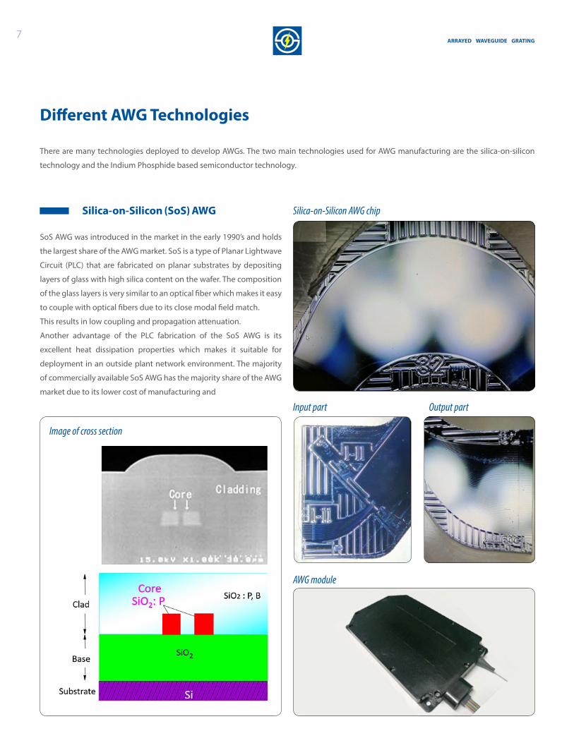
There are many technologies deployed to develop AWGs. The two main technologies used for AWG manufacturing are the silica-on-silicon
technology and the Indium Phosphide based semiconductor technology.
SoS AWG was introduced in the market in the early 1990’s and holds
the largest share of the AWG market. SoS is a type of Planar Lightwave
Circuit (PLC) that are fabricated on planar substrates by depositing
layers of glass with high silica content on the wafer. The composition
of the glass layers is very similar to an optical fiber which makes it easy
to couple with optical fibers due to its close modal field match.
This results in low coupling and propagation attenuation.
Another advantage of the PLC fabrication of the SoS AWG is its
excellent heat dissipation properties which makes it suitable for
deployment in an outside plant network environment. The majority
of commercially available SoS AWG has the majority share of the AWG
market due to its lower cost of manufacturing and
Different AWG Technologies
Silica-on-Silicon (SoS) AWG
Input part Output part
AWG module
Silica-on-Silicon AWG chip
Image of cross section
8ArrAyed WAveguide grAting
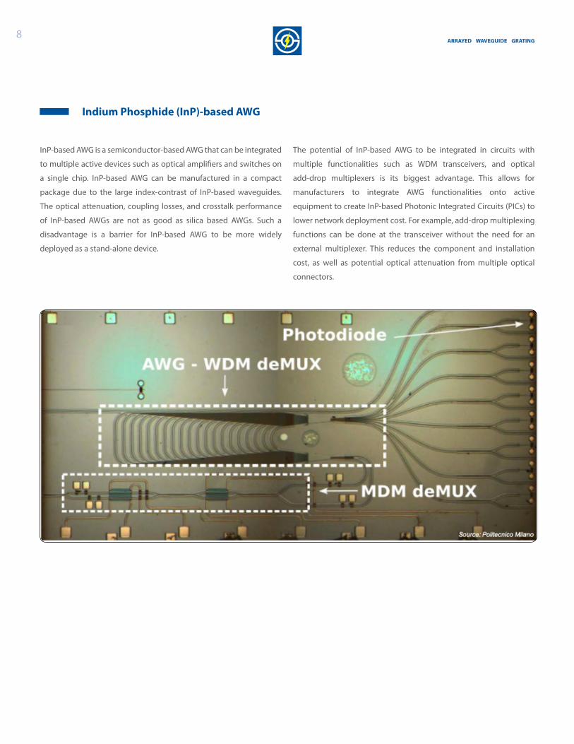
InP-based AWG is a semiconductor-based AWG that can be integrated
to multiple active devices such as optical amplifiers and switches on
a single chip. InP-based AWG can be manufactured in a compact
package due to the large index-contrast of InP-based waveguides.
The optical attenuation, coupling losses, and crosstalk performance
of InP-based AWGs are not as good as silica based AWGs. Such a
disadvantage is a barrier for InP-based AWG to be more widely
deployed as a stand-alone device.
The potential of InP-based AWG to be integrated in circuits with
multiple functionalities such as WDM transceivers, and optical
add-drop multiplexers is its biggest advantage. This allows for
manufacturers to integrate AWG functionalities onto active
equipment to create InP-based Photonic Integrated Circuits (PICs) to
lower network deployment cost. For example, add-drop multiplexing
functions can be done at the transceiver without the need for an
external multiplexer. This reduces the component and installation
cost, as well as potential optical attenuation from multiple optical
connectors.
Indium Phosphide (InP)-based AWG
9ArrAyed WAveguide grAting
Applications
There are a large number of applications where AWGs can
be deployed, ranging from complex telecommunication
cross-connects to very simple add-drop multiplexers. In the
telecommunication industry, AWGs are mostly used as (de)
multiplexers in WDM networks. This is traditionally deployed in long-
haul networks such as international, national, and regional transport
networks.
The majority of Passive Optical Networks (PON) deployed globally uses
wavelength-independent optical splitter for power splitting and time
division multiplexing for upstream and downstream transmission.
This enables a lower cost of deployment and removes the need to
manage wavelengths to individual connections downstream from
the optical splitter.
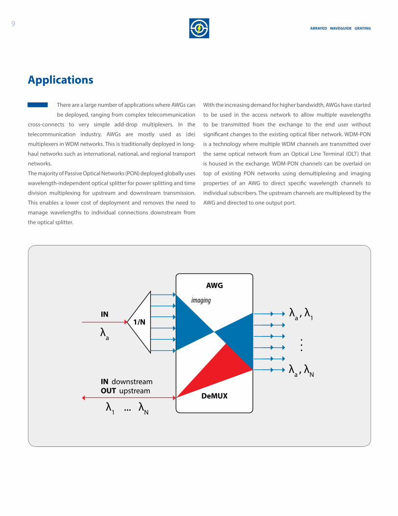
With the increasing demand for higher bandwidth, AWGs have started
to be used in the access network to allow multiple wavelengths
to be transmitted from the exchange to the end user without
significant changes to the existing optical fiber network. WDM-PON
is a technology where multiple WDM channels are transmitted over
the same optical network from an Optical Line Terminal (OLT) that
is housed in the exchange. WDM-PON channels can be overlaid on
top of existing PON networks using demultiplexing and imaging
properties of an AWG to direct specific wavelength channels to
individual subscribers. The upstream channels are multiplexed by the
AWG and directed to one output port.
AWG
IN
IN downstreamOUT upstream
λa
λa , λ1
...
λa , λN
λ1 ... λN
imaging
DeMUX
1/N
10ArrAyed WAveguide grAting
Mobile Fronthaul Network
Mobile communications have evolved from a simple voice application to high speed data networks. Mobile
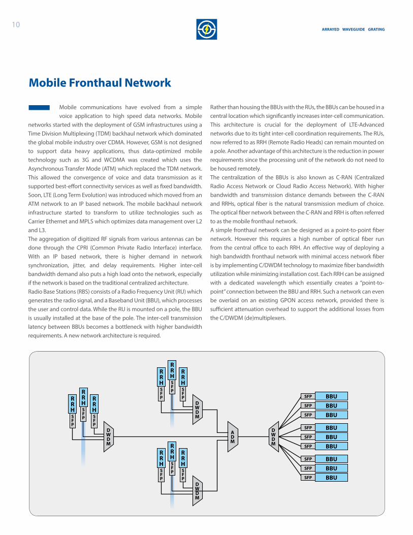
networks started with the deployment of GSM infrastructures using a Time Division Multiplexing (TDM) backhaul network which dominated the global mobile industry over CDMA. However, GSM is not designed to support data heavy applications, thus data-optimized mobile technology such as 3G and WCDMA was created which uses the Asynchronous Transfer Mode (ATM) which replaced the TDM network. This allowed the convergence of voice and data transmission as it supported best-effort connectivity services as well as fixed bandwidth. Soon, LTE (Long Term Evolution) was introduced which moved from an ATM network to an IP based network. The mobile backhaul network infrastructure started to transform to utilize technologies such as Carrier Ethernet and MPLS which optimizes data management over L2 and L3. The aggregation of digitized RF signals from various antennas can be done through the CPRI (Common Private Radio Interface) interface. With an IP based network, there is higher demand in network synchronization, jitter, and delay requirements. Higher inter-cell bandwidth demand also puts a high load onto the network, especially if the network is based on the traditional centralized architecture. Radio Base Stations (RBS) consists of a Radio Frequency Unit (RU) which generates the radio signal, and a Baseband Unit (BBU), which processes the user and control data. While the RU is mounted on a pole, the BBU is usually installed at the base of the pole. The inter-cell transmission latency between BBUs becomes a bottleneck with higher bandwidth requirements. A new network architecture is required.
Rather than housing the BBUs with the RUs, the BBUs can be housed in a central location which significantly increases inter-cell communication. This architecture is crucial for the deployment of LTE-Advanced networks due to its tight inter-cell coordination requirements. The RUs, now referred to as RRH (Remote Radio Heads) can remain mounted on a pole. Another advantage of this architecture is the reduction in power requirements since the processing unit of the network do not need to be housed remotely. The centralization of the BBUs is also known as C-RAN (Centralized Radio Access Network or Cloud Radio Access Network). With higher bandwidth and transmission distance demands between the C-RAN and RRHs, optical fiber is the natural transmission medium of choice. The optical fiber network between the C-RAN and RRH is often referred to as the mobile fronthaul network. A simple fronthaul network can be designed as a point-to-point fiber network. However this requires a high number of optical fiber run from the central office to each RRH. An effective way of deploying a high bandwidth fronthaul network with minimal access network fiber is by implementing C/DWDM technology to maximize fiber bandwidth utilization while minimizing installation cost. Each RRH can be assigned with a dedicated wavelength which essentially creates a “point-to-point” connection between the BBU and RRH. Such a network can even be overlaid on an existing GPON access network, provided there is sufficient attenuation overhead to support the additional losses from the C/DWDM (de)multiplexers.
RRHSFP
RRHSFP
RRHSFP
DWDM
RRHSFP
RRHSFP
RRHSFP
DWDM
ADM
RRHSFP
RRHSFP
RRHSFP
DWDM
BBUSFP
BBUSFP
BBUSFP
BBUSFP
BBUSFP
BBUSFP
BBUSFP
BBUSFP
BBUSFP
DWDM
11ArrAyed WAveguide grAting
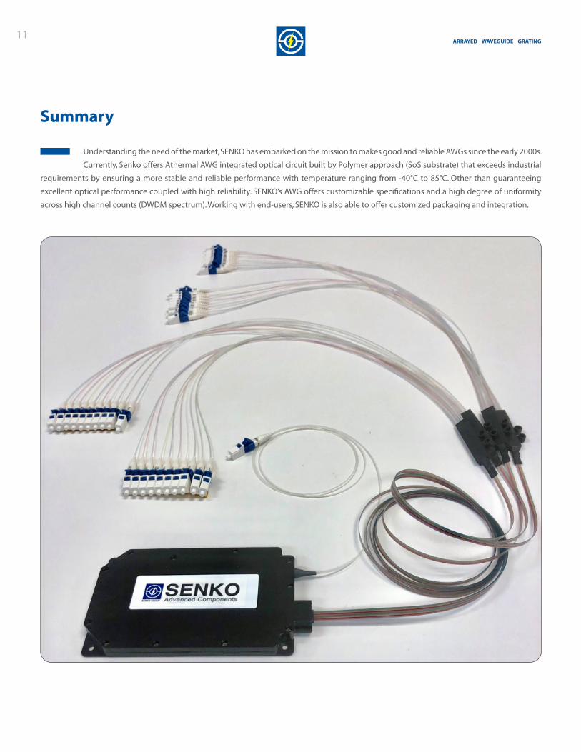
Understanding the need of the market, SENKO has embarked on the mission to makes good and reliable AWGs since the early 2000s.
Currently, Senko offers Athermal AWG integrated optical circuit built by Polymer approach (SoS substrate) that exceeds industrial
requirements by ensuring a more stable and reliable performance with temperature ranging from -40°C to 85°C. Other than guaranteeing
excellent optical performance coupled with high reliability. SENKO’s AWG offers customizable specifications and a high degree of uniformity
across high channel counts (DWDM spectrum). Working with end-users, SENKO is also able to offer customized packaging and integration.
Summary
12ArrAyed WAveguide grAting
• Xaveer J. M. Leijtens, Berndt Kuhlow and Meint K. Smit, Arrayed Waveguide Gratings, Eindhoven University of Technology, 2006
• Self-Seeded RSOAs WDM PON field trial for business and mobile fronthaul applications, Optical Society of America
• Enabling Cloud-RAN with Mobile Fronthaul, Mobile operators to migrate small and micro cells to a cloud-RAN architecture, Infinera.
• www.submarinecablemap.com
References
Biography
Dr. Bernard HL Lee is currently the Regional Technology Director at SENKO Advanced Components. He started his career in optical communications when he was appointed as a Senior Research Office for the European Union IST project known as DAVID in 2000. In 2003, he joined Telekom Malaysia R&D where he has held various technical and management positions there including the Head of Photonic Network Research and also Head of Innovation and Communications. Bernard then joined the parent company, Telekom Malaysia (TM) in 2010 as the Assistant General Manager of the Group Business Strategy Division where he oversees the company’s business direction. Bernard obtained his RCDD accreditation in 2016. Bernard is also a member of the International Electrotechnical Commission (IEC), the Institute of Engineering and Technology (IET) and was also the Director of the Board of the Fiber-To-The-Home Council APAC. He is currently the Malaysia Country Chair for BICSI Southeast Asia.
Ryo Konno is currently the Product Line Manager at SENKO Advanced Components. With the extensive sales experience in Japan, UK, and USA, he took lead on sales strategy and established great relationships with major equipment companies. He also gained unique view of developing new Fiber Optical components which contribute to space saving, higher density and maintain high reliability serving critical role in next generation optical module to support 5G and 400G+. Ryo is also a member of Gen-Z and Open Compute Project (OCP).
Mac Watanabe, master of engineering, senior product engineer at SENKO advanced Components. He has more than 25years experiences for fiber optics industry, researched and established for PLC splitter assembly technologies in early stage on 1990s before FTTH movement rises. He had unique working experiences in Japan, United states and China, linked as Learned background technologies, Grown with the latest marketing and Great tact of mass manufacturing. Through several years freelance engineer experiences were also helping his all balanced skills. Currently is investigating with new product development of fiber optics related for passive and active components.
13ArrAyed WAveguide grAting