Embed Size (px)
Citation preview
Arria 10 Device Overview2016.10.31
A10-OVERVIEW Subscribe Send Feedback
The Arria® 10 device family consists of high-performance and power-efficient 20 nm mid-range FPGAsand SoCs.
Arria 10 device family delivers:
• Higher performance than the previous generation of mid-range and high-end FPGAs.• Power efficiency attained through a comprehensive set of power-saving technologies.
The Arria 10 devices are ideal for high performance, power-sensitive, midrange applications in diversemarkets.
Table 1: Sample Markets and Ideal Applications for Arria 10 Devices
Market Applications
Wireless • Channel and switch cards in remote radio heads• Mobile backhaul
Wireline • 40G/100G muxponders and transponders• 100G line cards• Bridging• Aggregation
Broadcast • Studio switches• Servers and transport• Videoconferencing• Professional audio and video
Computing and Storage • Flash cache• Cloud computing servers• Server acceleration
Medical • Diagnostic scanners• Diagnostic imaging
© 2016 Intel Corporation. All rights reserved. Intel, the Intel logo, Altera, Arria, Cyclone, Enpirion, MAX, Megacore, NIOS, Quartus and Stratix words and logosare trademarks of Intel Corporation in the US and/or other countries. Other marks and brands may be claimed as the property of others. Intel warrantsperformance of its FPGA and semiconductor products to current specifications in accordance with Intel's standard warranty, but reserves the right to makechanges to any products and services at any time without notice. Intel assumes no responsibility or liability arising out of the application or use of anyinformation, product, or service described herein except as expressly agreed to in writing by Intel. Intel customers are advised to obtain the latest version ofdevice specifications before relying on any published information and before placing orders for products or services.
ISO9001:2008Registered
www.altera.com101 Innovation Drive, San Jose, CA 95134

Market Applications
Military • Missile guidance and control• Radar• Electronic warfare• Secure communications
Related InformationArria 10 Device Handbook: Known IssuesLists the planned updates to the Arria 10 Device Handbook chapters.
Key Advantages of Arria 10 Devices
Table 2: Key Advantages of the Arria 10 Device Family
Advantage Supporting Feature
Enhanced core architecture • Built on TSMC's 20 nm process technology• 60% higher performance than the previous generation of mid-
range FPGAs• 15% higher performance than the fastest previous-generation
FPGA
High-bandwidth integratedtransceivers
• Short-reach rates up to 25.8 Gigabits per second (Gbps)• Backplane capability up to 17.4 Gbps• Integrated 10GBASE-KR and 40GBASE-KR4 Forward Error
Correction (FEC)
Improved logic integration and hardIP blocks
• 8-input adaptive logic module (ALM)• Up to 65.6 megabits (Mb) of embedded memory• Variable-precision digital signal processing (DSP) blocks• Fractional synthesis phase-locked loops (PLLs)• Hard PCI Express Gen3 IP blocks• Hard memory controllers and PHY up to 2,666 Megabits per
second (Mbps)
Second generation hard processorsystem (HPS) with integrated ARM®
Cortex™-A9 MPCore processor
• Tight integration of a dual-core ARM Cortex-A9 MPCoreprocessor, hard IP, and an FPGA in a single Arria 10 system-on-a-chip (SoC)
• Supports over 128 Gbps peak bandwidth with integrated datacoherency between the processor and the FPGA fabric
2 Key Advantages of Arria 10 DevicesA10-OVERVIEW
2016.10.31
Altera Corporation Arria 10 Device Overview
Send Feedback
Advantage Supporting Feature
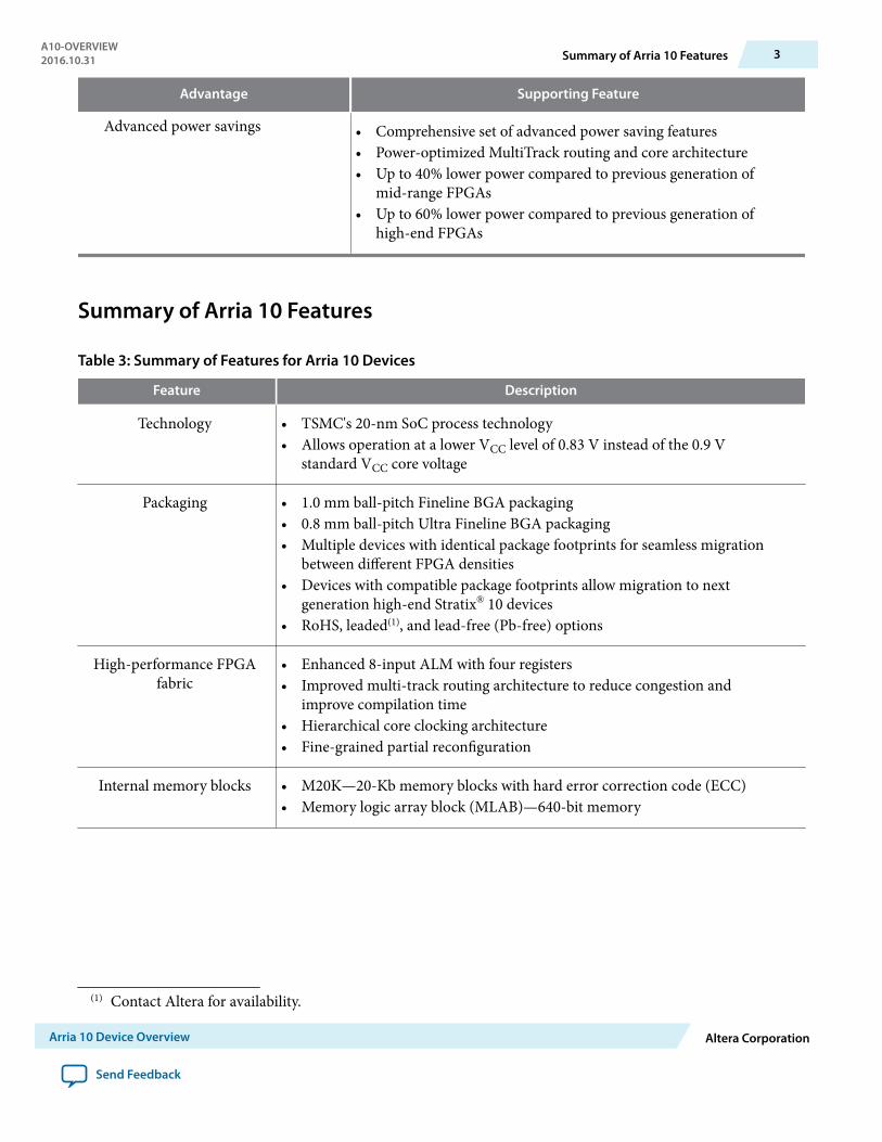
Advanced power savings • Comprehensive set of advanced power saving features• Power-optimized MultiTrack routing and core architecture• Up to 40% lower power compared to previous generation of
mid-range FPGAs• Up to 60% lower power compared to previous generation of
high-end FPGAs
Summary of Arria 10 Features
Table 3: Summary of Features for Arria 10 Devices
Feature Description
Technology • TSMC's 20-nm SoC process technology• Allows operation at a lower VCC level of 0.83 V instead of the 0.9 V
standard VCC core voltage
Packaging • 1.0 mm ball-pitch Fineline BGA packaging• 0.8 mm ball-pitch Ultra Fineline BGA packaging• Multiple devices with identical package footprints for seamless migration
between different FPGA densities• Devices with compatible package footprints allow migration to next
generation high-end Stratix® 10 devices• RoHS, leaded(1), and lead-free (Pb-free) options
High-performance FPGAfabric
• Enhanced 8-input ALM with four registers• Improved multi-track routing architecture to reduce congestion and
improve compilation time• Hierarchical core clocking architecture• Fine-grained partial reconfiguration
Internal memory blocks • M20K—20-Kb memory blocks with hard error correction code (ECC)• Memory logic array block (MLAB)—640-bit memory
(1) Contact Altera for availability.
A10-OVERVIEW2016.10.31 Summary of Arria 10 Features 3
Arria 10 Device Overview Altera Corporation
Send Feedback
Feature Description
Embedded Hard IP blocks
Variable-precisionDSP
• Native support for signal processing precision levelsfrom 18 x 19 to 54 x 54
• Native support for 27 x 27 multiplier mode• 64-bit accumulator and cascade for systolic finite
impulse responses (FIRs)• Internal coefficient memory banks• Preadder/subtractor for improved efficiency• Additional pipeline register to increase performance
and reduce power• Supports floating point arithmetic:
• Perform multiplication, addition, subtraction,multiply-add, multiply-subtract, and complexmultiplication.
• Supports multiplication with accumulationcapability, cascade summation, and cascadesubtraction capability.
• Dynamic accumulator reset control.• Support direct vector dot and complex multiplica‐
tion chaining multiply floating point DSP blocks.
Memory controller DDR4, DDR3, and DDR3L
PCI Express®PCI Express (PCIe®) Gen3 (x1, x2, x4, or x8), Gen2 (x1,x2, x4, or x8) and Gen1 (x1, x2, x4, or x8) hard IP withcomplete protocol stack, endpoint, and root port
Transceiver I/O • 10GBASE-KR/40GBASE-KR4 Forward ErrorCorrection (FEC)
• PCS hard IPs that support:
• 10-Gbps Ethernet (10GbE)• PCIe PIPE interface• Interlaken• Gbps Ethernet (GbE)• Common Public Radio Interface (CPRI) with
deterministic latency support• Gigabit-capable passive optical network (GPON)
with fast lock-time support• 13.5G JESD204b• 8B/10B, 64B/66B, 64B/67B encoders and decoders• Custom mode support for proprietary protocols
4 Summary of Arria 10 FeaturesA10-OVERVIEW
2016.10.31
Altera Corporation Arria 10 Device Overview
Send Feedback
Feature Description
Core clock networks • Up to 800 MHz fabric clocking, depending on the application:
• 667 MHz external memory interface clocking with 2,666 Mbps DDR4interface
• 800 MHz LVDS interface clocking with 1,600 Mbps LVDS interface• Global, regional, and peripheral clock networks• Clock networks that are not used can be gated to reduce dynamic power
Phase-locked loops (PLLs) • High-resolution fractional synthesis PLLs:
• Precision clock synthesis, clock delay compensation, and zero delaybuffering (ZDB)
• Support integer mode and fractional mode• Fractional mode support with third-order delta-sigma modulation
• Integer PLLs:
• Adjacent to general purpose I/Os• Support external memory and LVDS interfaces
FPGA General-purpose I/Os(GPIOs)
• 1.6 Gbps LVDS—every pair can be configured as receiver or transmitter• On-chip termination (OCT)• 1.2 V to 3.0 V single-ended LVTTL/LVCMOS interfacing
External Memory Interface • Hard memory controller— DDR4, DDR3, and DDR3L support
• DDR4—speeds up to 1,333 MHz/2,666 Mbps• DDR3—speeds up to 1,067 MHz/2,133 Mbps
• Soft memory controller—provides support for RLDRAM 3(2), QDR IV(2),and QDR II+
(2) Arria 10 devices support this external memory interface using hard PHY with soft memory controller.
A10-OVERVIEW2016.10.31 Summary of Arria 10 Features 5
Arria 10 Device Overview Altera Corporation
Send Feedback
Feature Description
Low-power serial transceivers • Continuous operating range:
• Arria 10 GX—1 Gbps to 17.4 Gbps• Arria 10 GT—1 Gbps to 25.8 Gbps
• Backplane support:
• Arria 10 GX—up to 16.0 Gbps• Arria 10 GT—up to 17.4 Gbps
• Extended range down to 125 Mbps with oversampling• ATX transmit PLLs with user-configurable fractional synthesis capability• Electronic Dispersion Compensation (EDC) support for XFP, SFP+, QSFP,
and CFP optical module• Adaptive linear and decision feedback equalization• Transmitter pre-emphasis and de-emphasis• Dynamic partial reconfiguration of individual transceiver channels• On-chip instrumentation (EyeQ non-intrusive data eye monitoring)
6 Summary of Arria 10 FeaturesA10-OVERVIEW
2016.10.31
Altera Corporation Arria 10 Device Overview
Send Feedback
Feature Description
HPS
(Arria 10 SX devices only)
Processor andsystem
• Dual-core ARM Cortex-A9 MPCore processor—1.2 GHz CPU with 1.5 GHz overdrive capability
• 256 KB on-chip RAM and 64 KB on-chip ROM• System peripherals—general-purpose timers,
watchdog timers, direct memory access (DMA)controller, FPGA configuration manager, and clockand reset managers
• Security features—anti-tamper, secure boot,Advanced Encryption Standard (AES) and authentica‐tion (SHA)
• ARM CoreSight™ JTAG debug access port, trace port,and on-chip trace storage
External interfaces • Hard memory interface—Hard memory controller(2,666 Mbps DDR4, and 2,166 Mbps DDR3), Quadserial peripheral interface (QSPI) flash controller,NAND flash controller, direct memory access (DMA)controller, Secure Digital/MultiMediaCard(SD/MMC) controller
• Communication interface— 10/100/1000 Ethernetmedia access control (MAC), USB On-The-GO(OTG) controllers, I2C controllers, UART 16550,serial peripheral interface (SPI), and up to 62HPS GPIO interfaces (48 direct-share I/Os)
Interconnects tocore
• High-performance ARM AMBA® AXI bus bridgesthat support simultaneous read and write
• HPS–FPGA bridges—include the FPGA-to-HPS,HPS-to-FPGA, and lightweight HPS-to-FPGA bridgesthat allow the FPGA fabric to issue transactions toslaves in the HPS, and vice versa
• Configuration bridge that allows HPS configurationmanager to configure the core logic via dedicated 32-bit configuration port
• FPGA-to-HPS SDRAM controller bridge—providesconfiguration interfaces for the multiport front end(MPFE) of the HPS SDRAM controller
A10-OVERVIEW2016.10.31 Summary of Arria 10 Features 7
Arria 10 Device Overview Altera Corporation
Send Feedback
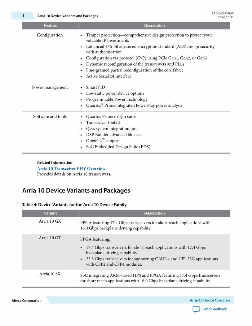
Feature Description
Configuration • Tamper protection—comprehensive design protection to protect yourvaluable IP investments
• Enhanced 256-bit advanced encryption standard (AES) design securitywith authentication
• Configuration via protocol (CvP) using PCIe Gen1, Gen2, or Gen3• Dynamic reconfiguration of the transceivers and PLLs• Fine-grained partial reconfiguration of the core fabric• Active Serial x4 Interface
Power management • SmartVID• Low static power device options• Programmable Power Technology• Quartus® Prime integrated PowerPlay power analysis
Software and tools • Quartus Prime design suite• Transceiver toolkit• Qsys system integration tool• DSP Builder advanced blockset• OpenCL™ support• SoC Embedded Design Suite (EDS)
Related InformationArria 10 Transceiver PHY OverviewProvides details on Arria 10 transceivers.
Arria 10 Device Variants and Packages
Table 4: Device Variants for the Arria 10 Device Family
Variant Description
Arria 10 GX FPGA featuring 17.4 Gbps transceivers for short reach applications with16.0 Gbps backplane driving capability.
Arria 10 GT FPGA featuring:
• 17.4 Gbps transceivers for short reach applications with 17.4 Gbpsbackplane driving capability.
• 25.8 Gbps transceivers for supporting CAUI-4 and CEI-25G applicationswith CFP2 and CFP4 modules.
Arria 10 SX SoC integrating ARM-based HPS and FPGA featuring 17.4 Gbps transceiversfor short reach applications with 16.0 Gbps backplane driving capability.
8 Arria 10 Device Variants and PackagesA10-OVERVIEW
2016.10.31
Altera Corporation Arria 10 Device Overview
Send Feedback
Arria 10 GXThis section provides the available options, maximum resource counts, and package plan for theArria 10 GX devices.
The information in this section is correct at the time of publication. For the latest information and to getmore details, refer to the Altera Product Selector.
Related InformationAltera Product SelectorProvides the latest information on Altera products.
Available Options
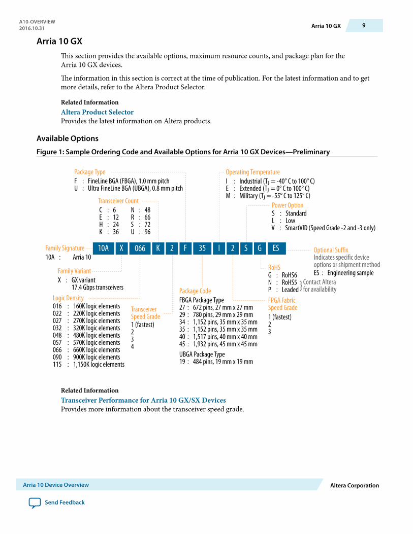
Figure 1: Sample Ordering Code and Available Options for Arria 10 GX Devices—Preliminary
Family Signature
Transceiver Count
TransceiverSpeed Grade
Package Type
Package Code
Operating Temperature
FPGA Fabric Speed Grade
Optional SuffixIndicates specific device options or shipment method
X : GX variant 17.4 Gbps transceivers
10A : Arria 10
016 : 160K logic elements022 : 220K logic elements027 : 270K logic elements032 : 320K logic elements048 : 480K logic elements057 : 570K logic elements066 : 660K logic elements090 : 900K logic elements115 : 1,150K logic elements
N : 48R : 66S : 72U : 96
C : 6E : 12H : 24K : 36
1 (fastest)
4
23
F : FineLine BGA (FBGA), 1.0 mm pitchU : Ultra FineLine BGA (UBGA), 0.8 mm pitch
FBGA Package Type27 : 672 pins, 27 mm x 27 mm29 : 780 pins, 29 mm x 29 mm34 : 1,152 pins, 35 mm x 35 mm35 : 1,152 pins, 35 mm x 35 mm40 : 1,517 pins, 40 mm x 40 mm45 : 1,932 pins, 45 mm x 45 mmUBGA Package Type19 : 484 pins, 19 mm x 19 mm
I : Industrial (TJ = -40° C to 100° C)E : Extended (TJ = 0° C to 100° C)M : Military (TJ = -55° C to 125° C)
1 (fastest)23
Power OptionS : StandardL
: Low
RoHSG : RoHS6N : RoHS5P : Leaded
ES : Engineering sample
10A X F066 K 2 S35 I 2 ESG
Logic Density
Family Variant
}Contact Alterafor availability
V
: SmartVID (Speed Grade -2 and -3 only)
Related InformationTransceiver Performance for Arria 10 GX/SX DevicesProvides more information about the transceiver speed grade.
A10-OVERVIEW2016.10.31 Arria 10 GX 9
Arria 10 Device Overview Altera Corporation
Send Feedback
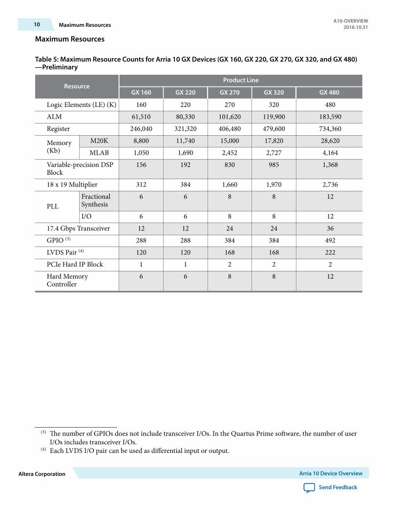
Maximum Resources
Table 5: Maximum Resource Counts for Arria 10 GX Devices (GX 160, GX 220, GX 270, GX 320, and GX 480)—Preliminary
ResourceProduct Line
GX 160 GX 220 GX 270 GX 320 GX 480
Logic Elements (LE) (K) 160 220 270 320 480ALM 61,510 80,330 101,620 119,900 183,590Register 246,040 321,320 406,480 479,600 734,360
Memory(Kb)
M20K 8,800 11,740 15,000 17,820 28,620MLAB 1,050 1,690 2,452 2,727 4,164
Variable-precision DSPBlock
156 192 830 985 1,368
18 x 19 Multiplier 312 384 1,660 1,970 2,736
PLLFractionalSynthesis
6 6 8 8 12
I/O 6 6 8 8 1217.4 Gbps Transceiver 12 12 24 24 36GPIO (3) 288 288 384 384 492LVDS Pair (4) 120 120 168 168 222PCIe Hard IP Block 1 1 2 2 2Hard MemoryController
6 6 8 8 12
(3) The number of GPIOs does not include transceiver I/Os. In the Quartus Prime software, the number of userI/Os includes transceiver I/Os.
(4) Each LVDS I/O pair can be used as differential input or output.
10 Maximum ResourcesA10-OVERVIEW
2016.10.31
Altera Corporation Arria 10 Device Overview
Send Feedback

Table 6: Maximum Resource Counts for Arria 10 GX Devices (GX 570, GX 660, GX 900, and GX 1150)—Preliminary
ResourceProduct Line
GX 570 GX 660 GX 900 GX 1150
Logic Elements (LE) (K) 570 660 900 1,150ALM 217,080 251,680 339,620 427,200Register 868,320 1,006,720 1,358,480 1,708,800
Memory(Kb)
M20K 36,000 42,620 48,460 54,260MLAB 5,096 5,788 9,386 12,984
Variable-precision DSPBlock
1,523 1,687 1,518 1,518
18 x 19 Multiplier 3,046 3,374 3,036 3,036
PLLFractionalSynthesis
16 16 32 32
I/O 16 16 16 1617.4 Gbps Transceiver 48 48 96 96GPIO (3) 696 696 768 768LVDS Pair (4) 324 324 384 384PCIe Hard IP Block 2 2 4 4Hard Memory Controller 16 16 16 16
Package Plan
Table 7: Package Plan for Arria 10 GX Devices (U19, F27, and F29) — Preliminary
Refer to I/O and High Speed I/O in Arria 10 Devices chapter for the number of 3 V I/O, LVDS I/O, andLVDS channels in each device package.
Product Line
U19
(19 mm × 19 mm,484-pin UBGA)
F27
(27 mm × 27 mm,672-pin FBGA)
F29
(29 mm × 29 mm, 780-pin FBGA)
3 V I/O LVDS I/O XCVR 3 V I/O LVDS I/O XCVR 3 V I/O LVDS I/O XCVR
GX 160 48 192 6 48 192 12 48 240 12GX 220 48 192 6 48 192 12 48 240 12GX 270 — — — 48 192 12 48 312 12GX 320 — — — 48 192 12 48 312 12GX 480 — — — — — — 48 312 12
A10-OVERVIEW2016.10.31 Package Plan 11
Arria 10 Device Overview Altera Corporation
Send Feedback
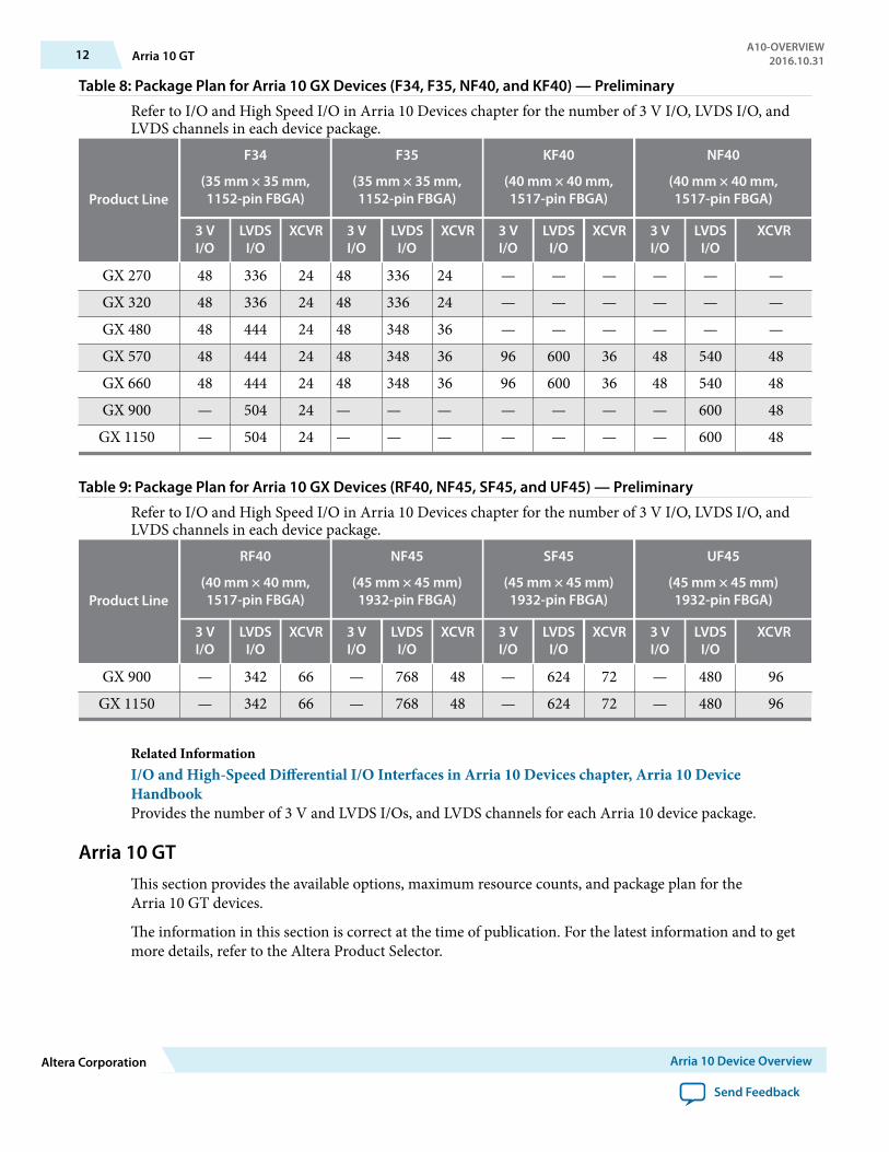
Table 8: Package Plan for Arria 10 GX Devices (F34, F35, NF40, and KF40) — Preliminary
Refer to I/O and High Speed I/O in Arria 10 Devices chapter for the number of 3 V I/O, LVDS I/O, andLVDS channels in each device package.
Product Line
F34
(35 mm × 35 mm,1152-pin FBGA)
F35
(35 mm × 35 mm,1152-pin FBGA)
KF40
(40 mm × 40 mm,1517-pin FBGA)
NF40
(40 mm × 40 mm,1517-pin FBGA)
3 VI/O
LVDSI/O
XCVR 3 VI/O
LVDSI/O
XCVR 3 VI/O
LVDSI/O
XCVR 3 VI/O
LVDSI/O
XCVR
GX 270 48 336 24 48 336 24 — — — — — —GX 320 48 336 24 48 336 24 — — — — — —GX 480 48 444 24 48 348 36 — — — — — —GX 570 48 444 24 48 348 36 96 600 36 48 540 48GX 660 48 444 24 48 348 36 96 600 36 48 540 48GX 900 — 504 24 — — — — — — — 600 48
GX 1150 — 504 24 — — — — — — — 600 48
Table 9: Package Plan for Arria 10 GX Devices (RF40, NF45, SF45, and UF45) — Preliminary
Refer to I/O and High Speed I/O in Arria 10 Devices chapter for the number of 3 V I/O, LVDS I/O, andLVDS channels in each device package.
Product Line
RF40
(40 mm × 40 mm,1517-pin FBGA)
NF45
(45 mm × 45 mm)1932-pin FBGA)
SF45
(45 mm × 45 mm)1932-pin FBGA)
UF45
(45 mm × 45 mm)1932-pin FBGA)
3 VI/O
LVDSI/O
XCVR 3 VI/O
LVDSI/O
XCVR 3 VI/O
LVDSI/O
XCVR 3 VI/O
LVDSI/O
XCVR
GX 900 — 342 66 — 768 48 — 624 72 — 480 96GX 1150 — 342 66 — 768 48 — 624 72 — 480 96
Related InformationI/O and High-Speed Differential I/O Interfaces in Arria 10 Devices chapter, Arria 10 DeviceHandbookProvides the number of 3 V and LVDS I/Os, and LVDS channels for each Arria 10 device package.
Arria 10 GTThis section provides the available options, maximum resource counts, and package plan for theArria 10 GT devices.
The information in this section is correct at the time of publication. For the latest information and to getmore details, refer to the Altera Product Selector.
12 Arria 10 GTA10-OVERVIEW
2016.10.31
Altera Corporation Arria 10 Device Overview
Send Feedback
Related InformationAltera Product SelectorProvides the latest information on Altera products.
Available Options
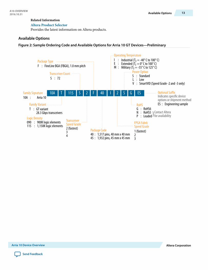
Figure 2: Sample Ordering Code and Available Options for Arria 10 GT Devices—Preliminary
Family Signature
Transceiver Count
TransceiverSpeed Grade
Package Type
Package Code
Operating Temperature
FPGA Fabric Speed Grade
Optional SuffixIndicates specific device options or shipment method
T : GT variant 28.3 Gbps transceivers
10A : Arria 10
090 : 900K logic elements115 : 1,150K logic elements
S : 72
2 (fastest) 34
F : FineLine BGA (FBGA), 1.0 mm pitch
40 : 1,517 pins, 40 mm x 40 mm45 : 1,932 pins, 45 mm x 45 mm
I : E : M :
1 (fastest)23
Power OptionS : StandardL : Low
RoHSG : RoHS6N : RoHS5P : Leaded
ES : Engineering sample
10A T F115 S 2 S40 I 2 ESG
Logic Density
Family Variant
}Contact Alterafor availability
Industrial (TJ = -40° C to 100° C)Extended (TJ = 0° C to 100° C)Military (TJ = -55° C to 125° C)
V
:
SmartVID (Speed Grade -2 and -3 only)
A10-OVERVIEW2016.10.31 Available Options 13
Arria 10 Device Overview Altera Corporation
Send Feedback
Maximum Resources
Table 10: Maximum Resource Counts for Arria 10 GT Devices—Preliminary
ResourceProduct Line
GT 900 GT 1150
Logic Elements (LE) (K) 900 1,150ALM 339,620 427,200Register 1,358,480 1,708,800
Memory (Kb)M20K 48,460 54,260MLAB 9,386 12,984
Variable-precision DSP Block 1,518 1,51818 x 19 Multiplier 3,036 3,036
PLLFractional Synthesis 32 32
I/O 16 16
Transceiver17.4 Gbps 72 (5) 72 (5)
25.8 Gbps 6 6GPIO(6) 624 624LVDS Pair(7) 312 312PCIe Hard IP Block 4 4Hard Memory Controller 16 16
Related InformationArria 10 GT Channel UsageConfiguring GT/GX channels in Arria 10 GT devices.
Package Plan
Table 11: Package Plan for Arria 10 GT Devices —Preliminary
Refer to I/O and High Speed I/O in Arria 10 Devices chapter for the number of 3 V I/O, LVDS I/O, andLVDS channels in each device package.
(5) If all 6 GT channels are in use, 12 of the GX channels are not usable.(6) The number of GPIOs does not include transceiver I/Os. In the Quartus Prime software, the number of user
I/Os includes transceiver I/Os.(7) Each LVDS I/O pair can be used as differential input or output.
14 Maximum ResourcesA10-OVERVIEW
2016.10.31
Altera Corporation Arria 10 Device Overview
Send Feedback
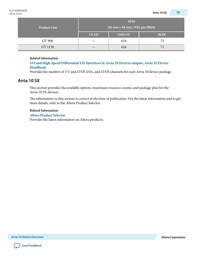
Product Line
SF45
(45 mm × 45 mm, 1932-pin FBGA)
3 V I/O LVDS I/O XCVR
GT 900 — 624 72GT 1150 — 624 72
Related InformationI/O and High-Speed Differential I/O Interfaces in Arria 10 Devices chapter, Arria 10 DeviceHandbookProvides the number of 3 V and LVDS I/Os, and LVDS channels for each Arria 10 device package.
Arria 10 SXThis section provides the available options, maximum resource counts, and package plan for theArria 10 SX devices.
The information in this section is correct at the time of publication. For the latest information and to getmore details, refer to the Altera Product Selector.
Related InformationAltera Product SelectorProvides the latest information on Altera products.
A10-OVERVIEW2016.10.31 Arria 10 SX 15
Arria 10 Device Overview Altera Corporation
Send Feedback
Available Options
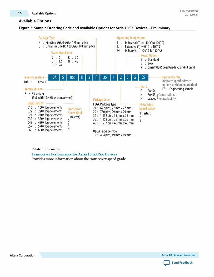
Figure 3: Sample Ordering Code and Available Options for Arria 10 SX Devices—Preliminary
Family Signature
Transceiver Count
TransceiverSpeed Grade
Package Type
Package Code
Operating Temperature
FPGA Fabric Speed Grade
Optional SuffixIndicates specific device options or shipment method
S : SX variant (SoC with 17.4 Gbps transceivers)
10A : Arria 10
016 : 160K logic elements022 : 220K logic elements027 : 270K logic elements032 : 320K logic elements048 : 480K logic elements057 : 570K logic elements066 : 660K logic elements
K : 36N : 48
C : 6E : 12H : 24
1 (fastest) 234
F : FineLine BGA (FBGA), 1.0 mm pitchU : Ultra FineLine BGA (UBGA), 0.8 mm pitch
FBGA Package Type27 : 672 pins, 27 mm x 27 mm29 : 780 pins, 29 mm x 29 mm34 : 1,152 pins, 35 mm x 35 mm35 : 1,152 pins, 35 mm x 35 mm40 : 1,517 pins, 40 mm x 40 mm
UBGA Package Type19 : 484 pins, 19 mm x 19 mm
I : E : M :
1 (fastest)23
Power OptionS : StandardL : Low
RoHSG : RoHS6N : RoHS5P : Leaded
ES : Engineering sample
10A S F066 K 2 S35 I 2 ESG
Logic Density
Family Variant
}Contact Alterafor availability
Industrial (TJ = -40° C to 100° C)Extended (TJ = 0° C to 100° C)Military (TJ = -55° C to 125° C)
V
:
SmartVID (Speed Grade -2 and -3 only)
Related InformationTransceiver Performance for Arria 10 GX/SX DevicesProvides more information about the transceiver speed grade.
16 Available OptionsA10-OVERVIEW
2016.10.31
Altera Corporation Arria 10 Device Overview
Send Feedback
Maximum Resources
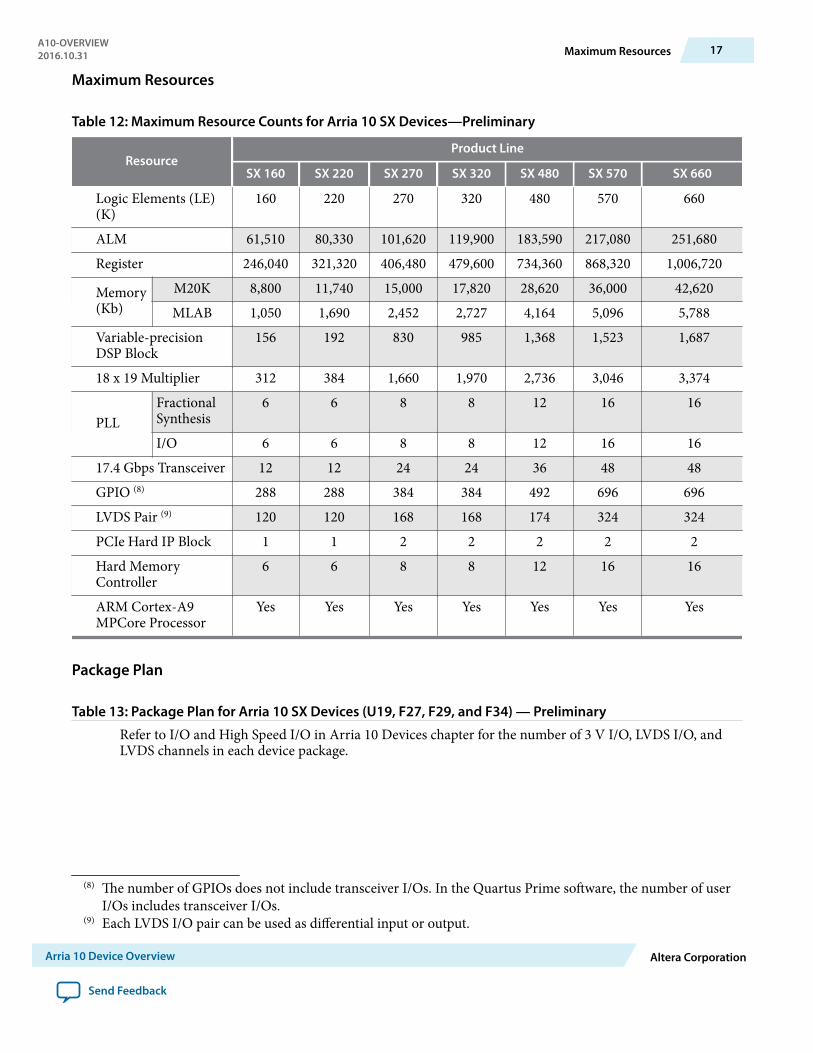
Table 12: Maximum Resource Counts for Arria 10 SX Devices—Preliminary
ResourceProduct Line
SX 160 SX 220 SX 270 SX 320 SX 480 SX 570 SX 660
Logic Elements (LE)(K)
160 220 270 320 480 570 660
ALM 61,510 80,330 101,620 119,900 183,590 217,080 251,680Register 246,040 321,320 406,480 479,600 734,360 868,320 1,006,720
Memory(Kb)
M20K 8,800 11,740 15,000 17,820 28,620 36,000 42,620MLAB 1,050 1,690 2,452 2,727 4,164 5,096 5,788
Variable-precisionDSP Block
156 192 830 985 1,368 1,523 1,687
18 x 19 Multiplier 312 384 1,660 1,970 2,736 3,046 3,374
PLLFractionalSynthesis
6 6 8 8 12 16 16
I/O 6 6 8 8 12 16 1617.4 Gbps Transceiver 12 12 24 24 36 48 48GPIO (8) 288 288 384 384 492 696 696LVDS Pair (9) 120 120 168 168 174 324 324PCIe Hard IP Block 1 1 2 2 2 2 2Hard MemoryController
6 6 8 8 12 16 16
ARM Cortex-A9MPCore Processor
Yes Yes Yes Yes Yes Yes Yes
Package Plan
Table 13: Package Plan for Arria 10 SX Devices (U19, F27, F29, and F34) — Preliminary
Refer to I/O and High Speed I/O in Arria 10 Devices chapter for the number of 3 V I/O, LVDS I/O, andLVDS channels in each device package.
(8) The number of GPIOs does not include transceiver I/Os. In the Quartus Prime software, the number of userI/Os includes transceiver I/Os.
(9) Each LVDS I/O pair can be used as differential input or output.
A10-OVERVIEW2016.10.31 Maximum Resources 17
Arria 10 Device Overview Altera Corporation
Send Feedback
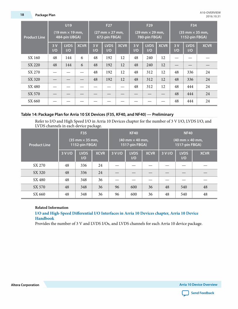
Product Line
U19
(19 mm × 19 mm,484-pin UBGA)
F27
(27 mm × 27 mm,672-pin FBGA)
F29
(29 mm × 29 mm,780-pin FBGA)
F34
(35 mm × 35 mm,1152-pin FBGA)
3 VI/O
LVDSI/O
XCVR 3 VI/O
LVDSI/O
XCVR 3 VI/O
LVDSI/O
XCVR 3 VI/O
LVDSI/O
XCVR
SX 160 48 144 6 48 192 12 48 240 12 — — —SX 220 48 144 6 48 192 12 48 240 12 — — —SX 270 — — — 48 192 12 48 312 12 48 336 24SX 320 — — — 48 192 12 48 312 12 48 336 24SX 480 — — — — — — 48 312 12 48 444 24SX 570 — — — — — — — — — 48 444 24SX 660 — — — — — — — — — 48 444 24
Table 14: Package Plan for Arria 10 SX Devices (F35, KF40, and NF40) — Preliminary
Refer to I/O and High Speed I/O in Arria 10 Devices chapter for the number of 3 V I/O, LVDS I/O, andLVDS channels in each device package.
Product Line
F35
(35 mm × 35 mm,1152-pin FBGA)
KF40
(40 mm × 40 mm,1517-pin FBGA)
NF40
(40 mm × 40 mm,1517-pin FBGA)
3 V I/O LVDSI/O
XCVR 3 V I/O LVDSI/O
XCVR 3 V I/O LVDSI/O
XCVR
SX 270 48 336 24 — — — — — —SX 320 48 336 24 — — — — — —SX 480 48 348 36 — — — — — —SX 570 48 348 36 96 600 36 48 540 48SX 660 48 348 36 96 600 36 48 540 48
Related InformationI/O and High-Speed Differential I/O Interfaces in Arria 10 Devices chapter, Arria 10 DeviceHandbookProvides the number of 3 V and LVDS I/Os, and LVDS channels for each Arria 10 device package.
18 Package PlanA10-OVERVIEW
2016.10.31
Altera Corporation Arria 10 Device Overview
Send Feedback
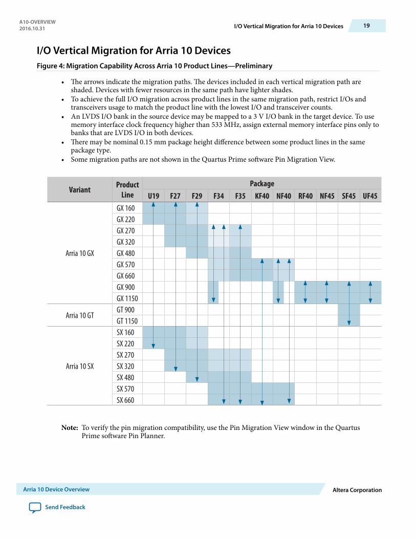
I/O Vertical Migration for Arria 10 DevicesFigure 4: Migration Capability Across Arria 10 Product Lines—Preliminary
• The arrows indicate the migration paths. The devices included in each vertical migration path areshaded. Devices with fewer resources in the same path have lighter shades.
• To achieve the full I/O migration across product lines in the same migration path, restrict I/Os andtransceivers usage to match the product line with the lowest I/O and transceiver counts.
• An LVDS I/O bank in the source device may be mapped to a 3 V I/O bank in the target device. To usememory interface clock frequency higher than 533 MHz, assign external memory interface pins only tobanks that are LVDS I/O in both devices.
• There may be nominal 0.15 mm package height difference between some product lines in the samepackage type.
• Some migration paths are not shown in the Quartus Prime software Pin Migration View.
Variant Product Line
PackageU19 F27 F29 F34 F35 KF40 NF40 RF40 NF45 SF45 UF45
Arria 10 GX
GX 160GX 220GX 270GX 320GX 480GX 570GX 660GX 900GX 1150
Arria 10 GTGT 900GT 1150
Arria 10 SX
SX 160SX 220SX 270SX 320SX 480SX 570SX 660
Note: To verify the pin migration compatibility, use the Pin Migration View window in the QuartusPrime software Pin Planner.
A10-OVERVIEW2016.10.31 I/O Vertical Migration for Arria 10 Devices 19
Arria 10 Device Overview Altera Corporation
Send Feedback
Migration between Arria 10 and Stratix 10 DevicesThere is footprint compatibility between Arria 10 and Stratix 10 packages. You can start developing yourdesign with selected Arria 10 devices and then move the design to Stratix 10 devices.
For details about the migration possibilities between the two device families, contact Altera.
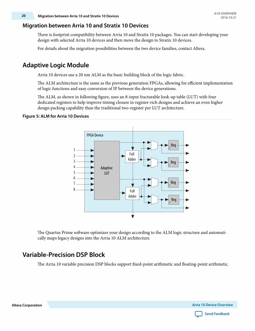
Adaptive Logic ModuleArria 10 devices use a 20 nm ALM as the basic building block of the logic fabric.
The ALM architecture is the same as the previous generation FPGAs, allowing for efficient implementationof logic functions and easy conversion of IP between the device generations.
The ALM, as shown in following figure, uses an 8-input fracturable look-up table (LUT) with fourdedicated registers to help improve timing closure in register-rich designs and achieve an even higherdesign packing capability than the traditional two-register per LUT architecture.
Figure 5: ALM for Arria 10 Devices
FPGA Device
12345678
Adaptive LUT
FullAdder
Reg
Reg
FullAdder
Reg
Reg
The Quartus Prime software optimizes your design according to the ALM logic structure and automati‐cally maps legacy designs into the Arria 10 ALM architecture.
Variable-Precision DSP BlockThe Arria 10 variable precision DSP blocks support fixed-point arithmetic and floating-point arithmetic.
20 Migration between Arria 10 and Stratix 10 DevicesA10-OVERVIEW
2016.10.31
Altera Corporation Arria 10 Device Overview
Send Feedback
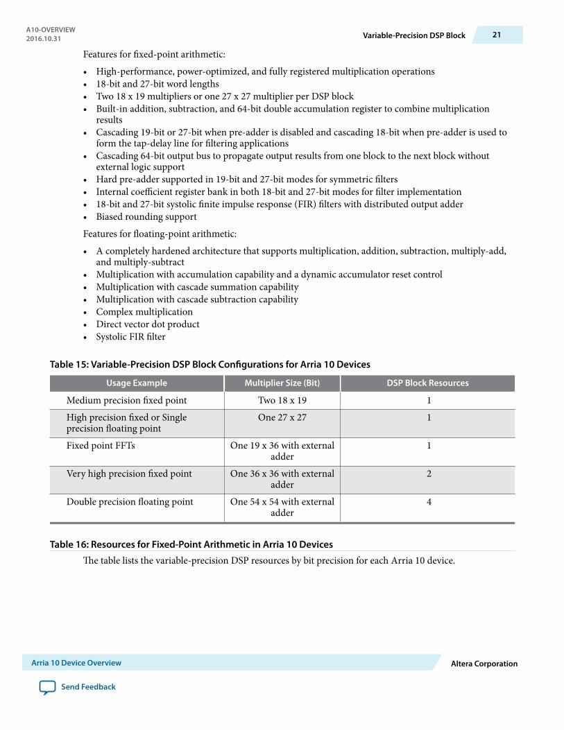
Features for fixed-point arithmetic:
• High-performance, power-optimized, and fully registered multiplication operations• 18-bit and 27-bit word lengths• Two 18 x 19 multipliers or one 27 x 27 multiplier per DSP block• Built-in addition, subtraction, and 64-bit double accumulation register to combine multiplication
results• Cascading 19-bit or 27-bit when pre-adder is disabled and cascading 18-bit when pre-adder is used to
form the tap-delay line for filtering applications• Cascading 64-bit output bus to propagate output results from one block to the next block without
external logic support• Hard pre-adder supported in 19-bit and 27-bit modes for symmetric filters• Internal coefficient register bank in both 18-bit and 27-bit modes for filter implementation• 18-bit and 27-bit systolic finite impulse response (FIR) filters with distributed output adder• Biased rounding support
Features for floating-point arithmetic:
• A completely hardened architecture that supports multiplication, addition, subtraction, multiply-add,and multiply-subtract
• Multiplication with accumulation capability and a dynamic accumulator reset control• Multiplication with cascade summation capability• Multiplication with cascade subtraction capability• Complex multiplication• Direct vector dot product• Systolic FIR filter
Table 15: Variable-Precision DSP Block Configurations for Arria 10 Devices
Usage Example Multiplier Size (Bit) DSP Block Resources
Medium precision fixed point Two 18 x 19 1High precision fixed or Singleprecision floating point
One 27 x 27 1
Fixed point FFTs One 19 x 36 with externaladder
1
Very high precision fixed point One 36 x 36 with externaladder
2
Double precision floating point One 54 x 54 with externaladder
4
Table 16: Resources for Fixed-Point Arithmetic in Arria 10 Devices
The table lists the variable-precision DSP resources by bit precision for each Arria 10 device.
A10-OVERVIEW2016.10.31 Variable-Precision DSP Block 21
Arria 10 Device Overview Altera Corporation
Send Feedback
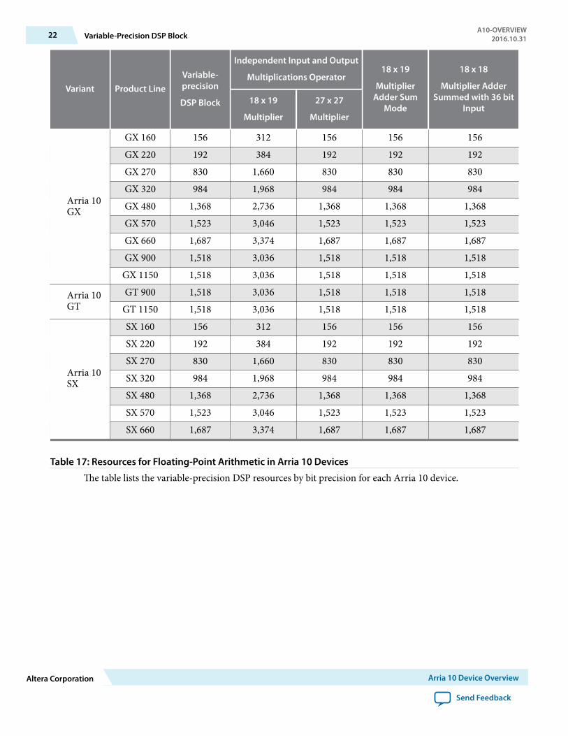
Variant Product LineVariable-precision
DSP Block
Independent Input and Output
Multiplications Operator18 x 19
MultiplierAdder Sum
Mode
18 x 18
Multiplier AdderSummed with 36 bit
Input18 x 19
Multiplier
27 x 27
Multiplier
Arria 10GX
GX 160 156 312 156 156 156GX 220 192 384 192 192 192GX 270 830 1,660 830 830 830GX 320 984 1,968 984 984 984GX 480 1,368 2,736 1,368 1,368 1,368GX 570 1,523 3,046 1,523 1,523 1,523GX 660 1,687 3,374 1,687 1,687 1,687GX 900 1,518 3,036 1,518 1,518 1,518
GX 1150 1,518 3,036 1,518 1,518 1,518
Arria 10GT
GT 900 1,518 3,036 1,518 1,518 1,518GT 1150 1,518 3,036 1,518 1,518 1,518
Arria 10SX
SX 160 156 312 156 156 156SX 220 192 384 192 192 192SX 270 830 1,660 830 830 830SX 320 984 1,968 984 984 984SX 480 1,368 2,736 1,368 1,368 1,368SX 570 1,523 3,046 1,523 1,523 1,523SX 660 1,687 3,374 1,687 1,687 1,687
Table 17: Resources for Floating-Point Arithmetic in Arria 10 Devices
The table lists the variable-precision DSP resources by bit precision for each Arria 10 device.
22 Variable-Precision DSP BlockA10-OVERVIEW
2016.10.31
Altera Corporation Arria 10 Device Overview
Send Feedback
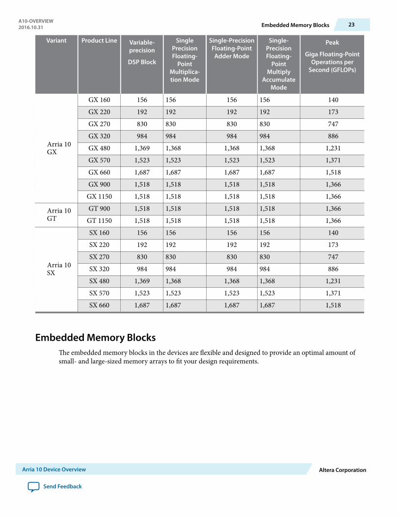
Variant Product Line Variable-precision
DSP Block
SinglePrecisionFloating-
PointMultiplica‐tion Mode
Single-PrecisionFloating-PointAdder Mode
Single-PrecisionFloating-
PointMultiply
AccumulateMode
Peak
Giga Floating-PointOperations per
Second (GFLOPs)
Arria 10GX
GX 160 156 156 156 156 140GX 220 192 192 192 192 173GX 270 830 830 830 830 747GX 320 984 984 984 984 886GX 480 1,369 1,368 1,368 1,368 1,231GX 570 1,523 1,523 1,523 1,523 1,371GX 660 1,687 1,687 1,687 1,687 1,518GX 900 1,518 1,518 1,518 1,518 1,366
GX 1150 1,518 1,518 1,518 1,518 1,366
Arria 10GT
GT 900 1,518 1,518 1,518 1,518 1,366GT 1150 1,518 1,518 1,518 1,518 1,366
Arria 10SX
SX 160 156 156 156 156 140SX 220 192 192 192 192 173SX 270 830 830 830 830 747SX 320 984 984 984 984 886SX 480 1,369 1,368 1,368 1,368 1,231SX 570 1,523 1,523 1,523 1,523 1,371SX 660 1,687 1,687 1,687 1,687 1,518
Embedded Memory BlocksThe embedded memory blocks in the devices are flexible and designed to provide an optimal amount ofsmall- and large-sized memory arrays to fit your design requirements.
A10-OVERVIEW2016.10.31 Embedded Memory Blocks 23
Arria 10 Device Overview Altera Corporation
Send Feedback
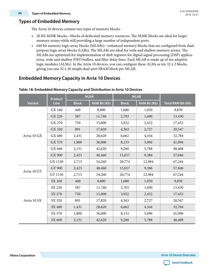
Types of Embedded MemoryThe Arria 10 devices contain two types of memory blocks:
• 20 Kb M20K blocks—blocks of dedicated memory resources. The M20K blocks are ideal for largermemory arrays while still providing a large number of independent ports.
• 640 bit memory logic array blocks (MLABs)—enhanced memory blocks that are configured from dual-purpose logic array blocks (LABs). The MLABs are ideal for wide and shallow memory arrays. TheMLABs are optimized for implementation of shift registers for digital signal processing (DSP) applica‐tions, wide and shallow FIFO buffers, and filter delay lines. Each MLAB is made up of ten adaptivelogic modules (ALMs). In the Arria 10 devices, you can configure these ALMs as ten 32 x 2 blocks,giving you one 32 x 20 simple dual-port SRAM block per MLAB.
Embedded Memory Capacity in Arria 10 Devices
Table 18: Embedded Memory Capacity and Distribution in Arria 10 Devices
VariantProduct
Line
M20K MLAB
Total RAM Bit (Kb)Block RAM Bit (Kb) Block RAM Bit (Kb)
Arria 10 GX
GX 160 440 8,800 1,680 1,050 9,850GX 220 587 11,740 2,703 1,690 13,430GX 270 750 15,000 3,922 2,452 17,452GX 320 891 17,820 4,363 2,727 20,547GX 480 1,431 28,620 6,662 4,164 32,784GX 570 1,800 36,000 8,153 5,096 41,096GX 660 2,131 42,620 9,260 5,788 48,408GX 900 2,423 48,460 15,017 9,386 57,846
GX 1150 2,713 54,260 20,774 12,984 67,244
Arria 10 GTGT 900 2,423 48,460 15,017 9,386 57,846
GT 1150 2,713 54,260 20,774 12,984 67,244
Arria 10 SX
SX 160 440 8,800 1,680 1,050 9,850SX 220 587 11,740 2,703 1,690 13,430SX 270 750 15,000 3,922 2,452 17,452SX 320 891 17,820 4,363 2,727 20,547SX 480 1,431 28,620 6,662 4,164 32,784SX 570 1,800 36,000 8,153 5,096 41,096SX 660 2,131 42,620 9,260 5,788 48,408
24 Types of Embedded MemoryA10-OVERVIEW
2016.10.31
Altera Corporation Arria 10 Device Overview
Send Feedback
Embedded Memory Configurations for Single-port Mode
Table 19: Single-port Embedded Memory Configurations for Arria 10 Devices
This table lists the maximum configurations supported for single-port RAM and ROM modes.Memory Block Depth (bits) Programmable Width
MLAB32 x16, x18, or x20
64(10) x8, x9, x10
M20K
512 x40, x321K x20, x162K x10, x84K x5, x48K x2
16K x1
Clock Networks and PLL Clock SourcesThe clock network architecture is based on Altera's global, regional, and peripheral clock structure. Thisclock structure is supported by dedicated clock input pins, fractional clock synthesis PLLs, and integer I/OPLLs.
Clock Networks
The Arria 10 core clock networks are capable of up to 800 MHz fabric operation across the full industrialtemperature range. For the external memory interface, the clock network supports the hard memorycontroller with speeds up to 2,666 Mbps in a quarter-rate transfer.
To reduce power consumption, the Quartus Prime software identifies all unused sections of the clocknetwork and powers them down.
Fractional Synthesis and I/O PLLsArria 10 devices contain up to 32 fractional synthesis PLLs and up to 16 I/O PLLs that are available forboth specific and general purpose uses in the core:
• Fractional synthesis PLLs - located in the column adjacent to the transceiver blocks• I/O PLLs - located in each bank of the 48 I/Os
Fractional Synthesis PLLs
You can use the fractional synthesis PLLs to:
• Reduce the number of oscillators that are required on your board• Reduce the number of clock pins that are used in the device by synthesizing multiple clock frequencies
from a single reference clock source
(10) Supported through software emulation and consumes additional MLAB blocks.
A10-OVERVIEW2016.10.31 Embedded Memory Configurations for Single-port Mode 25
Arria 10 Device Overview Altera Corporation
Send Feedback
The fractional synthesis PLLs support the following features:
• Reference clock frequency synthesis for transceiver CMU and Advanced Transmit (ATX) PLLs• Clock network delay compensation• Zero-delay buffering• Direct transmit clocking for transceivers• Independently configurable into two modes:
• Conventional integer mode equivalent to the general purpose PLL• Enhanced fractional mode with third order delta-sigma modulation
• PLL cascading
I/O PLLs
The integer mode I/O PLLs are located in each bank of 48 I/Os. You can use the I/O PLLs to simplify thedesign of external memory and high-speed LVDS interfaces.
In each I/O bank, the I/O PLLs are adjacent to the hard memory controllers and LVDS SERDES. Becausethese PLLs are tightly coupled with the I/Os that need to use them, it makes it easier to close timing.
You can use the I/O PLLs for general purpose applications in the core such as clock network delaycompensation and zero-delay buffering.
Arria 10 devices support PLL-to-PLL cascading.
FPGA General Purpose I/OArria 10 devices offer highly configurable GPIOs. Each I/O bank contains 48 general purpose I/Os and ahigh-efficiency hard memory controller.
The following list describes the features of the GPIOs:
• Consist of 3 V I/Os for high-voltage application and LVDS I/Os for differential signaling• Support a wide range of single-ended and differential I/O interfaces• LVDS speeds up to 1.6 Gbps• Each LVDS pair of pins has differential input and output buffers, allowing you to configure the LVDS
direction for each pair.• Programmable bus hold and weak pull-up• Programmable differential output voltage (VOD) and programmable pre-emphasis• Series (RS) and parallel (RT) on-chip termination (OCT) for all I/O banks with OCT calibration to
limit the termination impedance variation• On-chip dynamic termination that has the ability to swap between series and parallel termination,
depending on whether there is read or write on a common bus for signal integrity• Easy timing closure support using the hard read FIFO in the input register path, and delay-locked loop
(DLL) delay chain with fine and coarse architecture
External Memory InterfaceArria 10 devices offer massive external memory bandwidth, with up to seven 32-bit DDR4 memoryinterfaces running at up to 2,666 Mbps. This bandwidth provides additional ease of design, lower power,and resource efficiencies of hardened high-performance memory controllers.
26 FPGA General Purpose I/OA10-OVERVIEW
2016.10.31
Altera Corporation Arria 10 Device Overview
Send Feedback
The memory interface within Arria 10 FPGAs and SoCs delivers the highest performance and ease of use.You can configure up to a maximum width of 144 bits when using the hard or soft memory controllers. Ifrequired, you can bypass the hard memory controller and use a soft controller implemented in the userlogic.
Each I/O contains a hardened DDR read/write path (PHY) capable of performing key memory interfacefunctionality such as read/write leveling, FIFO buffering to lower latency and improve margin, timingcalibration, and on-chip termination.
The timing calibration is aided by the inclusion of hard microcontrollers based on Altera’s Nios® IItechnology, specifically tailored to control the calibration of multiple memory interfaces. This calibrationallows the Arria 10 device to compensate for any changes in process, voltage, or temperature either withinthe Arria 10 device itself, or within the external memory device. The advanced calibration algorithmsensure maximum bandwidth and robust timing margin across all operating conditions.
In addition to parallel memory interfaces, Arria 10 devices support serial memory technologies such as theHybrid Memory Cube (HMC). The HMC is supported by the Arria 10 high-speed serial transceiverswhich connect up to four HMC links, with each link running at data rates up to 15 Gbps.
Related InformationExternal Memory Interface Spec EstimatorProvides a parametric tool that allows you to find and compare the performance of the supported externalmemory interfaces in Altera devices.
Memory Standards Supported by Arria 10 DevicesThe I/Os are designed to provide high performance support for existing and emerging external memorystandards.
Table 20: Memory Standards Supported by the Hard Memory Controller
This table lists the overall capability of the hard memory controller. For specific details, refer to theExternal Memory Interface Spec Estimator and Arria 10 Device Datasheet.Memory Standard Rate Support Ping Pong PHY
SupportMaximum Frequency
(MHz)
DDR4 SDRAM Quarter rateYes 1,067
— 1,200
DDR3 SDRAM
Half rateYes 533
— 667
Quarter rateYes 1,067
— 1,067
DDR3L SDRAM
Half rateYes 533
— 667
Quarter rateYes 933
— 933
A10-OVERVIEW2016.10.31 Memory Standards Supported by Arria 10 Devices 27
Arria 10 Device Overview Altera Corporation
Send Feedback
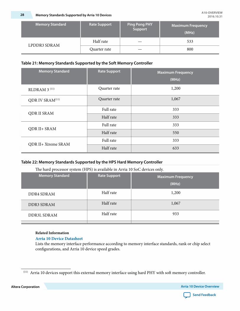
Memory Standard Rate Support Ping Pong PHYSupport
Maximum Frequency
(MHz)
LPDDR3 SDRAMHalf rate — 533
Quarter rate — 800
Table 21: Memory Standards Supported by the Soft Memory Controller
Memory Standard Rate Support Maximum Frequency
(MHz)
RLDRAM 3 (11) Quarter rate 1,200
QDR IV SRAM(11) Quarter rate 1,067
QDR II SRAMFull rate 333
Half rate 333
QDR II+ SRAMFull rate 333
Half rate 550
QDR II+ Xtreme SRAMFull rate 333
Half rate 633
Table 22: Memory Standards Supported by the HPS Hard Memory Controller
The hard processor system (HPS) is available in Arria 10 SoC devices only.Memory Standard Rate Support Maximum Frequency
(MHz)
DDR4 SDRAM Half rate 1,200
DDR3 SDRAM Half rate 1,067
DDR3L SDRAM Half rate 933
Related InformationArria 10 Device DatasheetLists the memory interface performance according to memory interface standards, rank or chip selectconfigurations, and Arria 10 device speed grades.
(11) Arria 10 devices support this external memory interface using hard PHY with soft memory controller.
28 Memory Standards Supported by Arria 10 DevicesA10-OVERVIEW
2016.10.31
Altera Corporation Arria 10 Device Overview
Send Feedback
PCIe Gen1, Gen2, and Gen3 Hard IPArria 10 devices contain PCIe hard IP that is designed for performance and ease-of-use:
• Includes all layers of the PCIe stack—transaction, data link and physical layers.• Supports PCIe Gen3, Gen2, and Gen1 Endpoint and Root Port in x1, x2, x4, or x8 lane configuration.• Operates independently from the core logic—optional configuration via protocol (CvP) allows the
PCIe link to power up and complete link training in less than 100 ms while the Arria 10 devicecompletes loading the programming file for the rest of the FPGA.
• Provides added functionality that makes it easier to support emerging features such as Single Root I/OVirtualization (SR-IOV) and optional protocol extensions.
• Provides improved end-to-end datapath protection using ECC.• Supports FPGA configuration via protocol (CvP) using PCIe at Gen3, Gen2, or Gen1 speed.
Related InformationPCS Features on page 35
Enhanced PCS Hard IP for Interlaken and 10 Gbps Ethernet
Interlaken SupportThe Arria 10 enhanced PCS hard IP provides integrated Interlaken PCS supporting rates up to 17.4 Gbpsper lane.
The Interlaken PCS is based on the proven functionality of the PCS developed for Altera’s previousgeneration FPGAs, which demonstrated interoperability with Interlaken ASSP vendors and third-party IPsuppliers. The Interlaken PCS is present in every transceiver channel in Arria 10 devices.
Related InformationPCS Features on page 35
10 Gbps Ethernet SupportThe Arria 10 enhanced PCS hard IP supports 10GBASE-R PCS compliant with IEEE 802.3 10 GbpsEthernet (10GbE). The integrated hard IP support for 10GbE and the 10 Gbps transceivers save externalPHY cost, board space, and system power.
The scalable hard IP supports multiple independent 10GbE ports while using a single PLL for all the10GBASE-R PCS instantiations, which saves on core logic resources and clock networks:
• Simplifies multiport 10GbE systems compared to XAUI interfaces that require an externalXAUI-to-10G PHY.
• Incorporates Electronic Dispersion Compensation (EDC), which enables direct connection to standard10 Gbps XFP and SFP+ pluggable optical modules.
• Supports backplane Ethernet applications and includes a hard 10GBASE-KR Forward Error Correction(FEC) circuit that you can use for 10 Gbps and 40 Gbps applications.
The 10 Gbps Ethernet PCS hard IP and 10GBASE-KR FEC are present in every transceiver channel.
A10-OVERVIEW2016.10.31 PCIe Gen1, Gen2, and Gen3 Hard IP 29
Arria 10 Device Overview Altera Corporation
Send Feedback

Related InformationPCS Features on page 35
Low Power Serial TransceiversArria 10 FPGAs and SoCs include lowest power transceivers that deliver high bandwidth, throughput andlow latency.
Arria 10 devices deliver the industry's lowest power consumption per transceiver channel:
• 12.5 Gbps transceivers at as low as 242 mW• 10 Gbps transceivers at as low as 168 mW• 6 Gbps transceivers at as low as 117 mW
Arria 10 transceivers support various data rates according to application:
• Chip-to-chip and chip-to-module applications—from 125 Mbps up to 25.8 Gbps• Long reach and backplane applications—from 125 Mbps up to 17.4 Gbps with advanced adaptive
equalization• Critical power sensitive applications—from 125 Mbps up to 11.3 Gbps using lower power modes
The combination of 20 nm process technology and architectural advances provide the following benefits:
• Significant reduction in die area and power consumption• Increase of up to two times in transceiver I/O density compared to previous generation devices while
maintaining optimal signal integrity• Up to 72 total transceiver channels—you can configure up to 6 of these channels to run as fast as
25.8 Gbps• All channels feature continuous data rate support up to the maximum rated speed
30 Low Power Serial TransceiversA10-OVERVIEW
2016.10.31
Altera Corporation Arria 10 Device Overview
Send Feedback
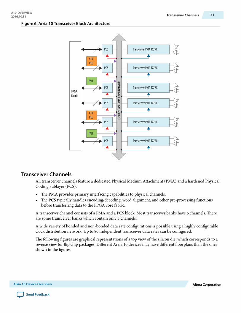
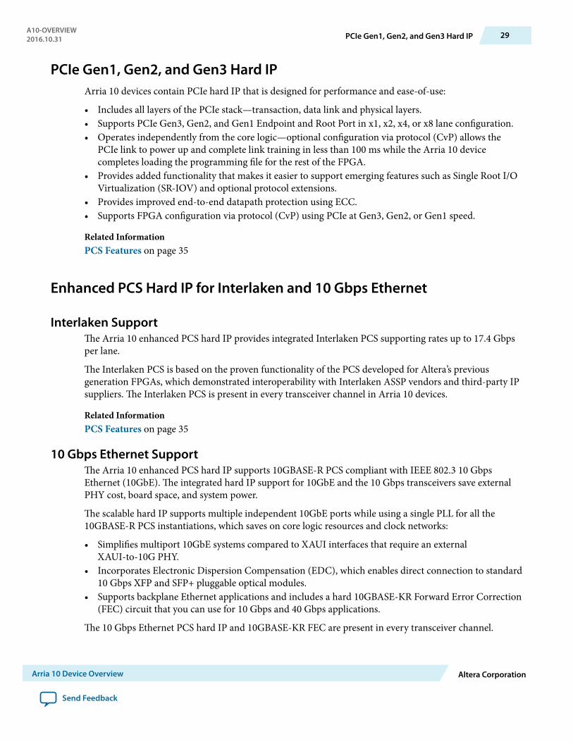
Figure 6: Arria 10 Transceiver Block Architecture
ATXPLL
fPLL
fPLL
ATXPLL
FPGAFabric
PCS
PCS
PCS
PCS
PCS
PCS
Transceiver PMA TX/RX
Transceiver PMA TX/RX
Transceiver PMA TX/RX
Transceiver PMA TX/RX
Transceiver PMA TX/RX
Transceiver PMA TX/RX
Flexib
le Clo
ck D
istrib
ution
Net
work
Transceiver ChannelsAll transceiver channels feature a dedicated Physical Medium Attachment (PMA) and a hardened PhysicalCoding Sublayer (PCS).
• The PMA provides primary interfacing capabilities to physical channels.• The PCS typically handles encoding/decoding, word alignment, and other pre-processing functions
before transferring data to the FPGA core fabric.
A transceiver channel consists of a PMA and a PCS block. Most transceiver banks have 6 channels. Thereare some transceiver banks which contain only 3 channels.
A wide variety of bonded and non-bonded data rate configurations is possible using a highly configurableclock distribution network. Up to 80 independent transceiver data rates can be configured.
The following figures are graphical representations of a top view of the silicon die, which corresponds to areverse view for flip chip packages. Different Arria 10 devices may have different floorplans than the onesshown in the figures.
A10-OVERVIEW2016.10.31 Transceiver Channels 31
Arria 10 Device Overview Altera Corporation
Send Feedback
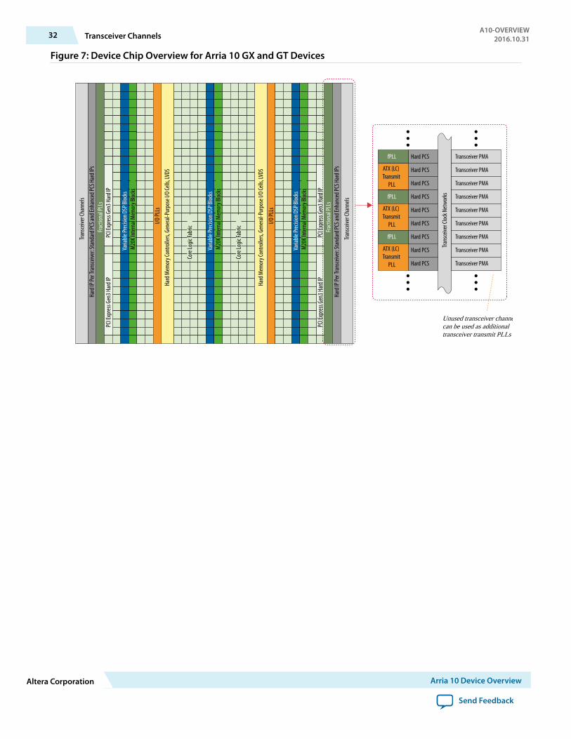
Figure 7: Device Chip Overview for Arria 10 GX and GT Devices
Core
Logic
Fabr
ic
M20
K Int
erna
l Mem
ory B
locks
Trans
ceive
r Cha
nnels
Hard
IP Pe
r Tra
nsce
iver:
Stan
dard
PCS a
nd En
hanc
ed PC
S Har
d IPs
PCI E
xpre
ss Ge
n3 H
ard I
PFra
ction
al PL
Ls
M20
K Int
erna
l Mem
ory B
locks
PCI E
xpre
ss Ge
n3 H
ard I
P
Varia
ble Pr
ecisi
on D
SP Bl
ocks
I/O PL
Ls
Hard
Mem
ory C
ontro
llers,
Gen
eral-
Purp
ose I
/O Ce
lls, L
VDS
M20
K Int
erna
l Mem
ory B
locks
M20
K Int
erna
l Mem
ory B
locks
Varia
ble Pr
ecisi
on D
SP Bl
ocks
Core
Logic
Fabr
ic
I/O PL
Ls
Hard
Mem
ory C
ontro
llers,
Gen
eral-
Purp
ose I
/O Ce
lls, L
VDS
M20
K Int
erna
l Mem
ory B
locks
M20
K Int
erna
l Mem
ory B
locks
Varia
ble Pr
ecisi
on D
SP Bl
ocks
Trans
ceive
r Cha
nnels
Hard
IP Pe
r Tra
nsce
iver:
Stan
dard
PCS a
nd En
hanc
ed PC
S Har
d IPs
PCI E
xpre
ss Ge
n3 H
ard I
PFra
ction
al PL
LsPC
I Exp
ress
Gen3
Har
d IP
Hard PCS
Hard PCS
Hard PCS
Hard PCS
Hard PCS
Hard PCS
Hard PCS
Hard PCS
Hard PCS Transceiver PMA
Transceiver PMA
Transceiver PMA
Transceiver PMA
Transceiver PMA
Transceiver PMA
Transceiver PMA
Transceiver PMA
Transceiver PMA
Trans
ceive
r Cloc
k Net
work
s
fPLL
ATX (LC)Transmit
PLL
fPLL
ATX (LC)Transmit
PLL
fPLL
ATX (LC)Transmit
PLL
Unused transceiver channelscan be used as additional transceiver transmit PLLs
32 Transceiver ChannelsA10-OVERVIEW
2016.10.31
Altera Corporation Arria 10 Device Overview
Send Feedback
Figure 8: Device Chip Overview for Arria 10 SX Devices
Core
Logic
Fabr
ic
M20
K Int
erna
l Mem
ory B
locks
Trans
ceive
r Cha
nnels
Hard
IP Pe
r Tra
nsce
iver:
Stan
dard
PCS a
nd En
hanc
ed PC
S Har
d IPs
PCI E
xpre
ss Ge
n3 H
ard I
PFra
ction
al PL
Ls
M20
K Int
erna
l Mem
ory B
locks
PCI E
xpre
ss Ge
n3 H
ard I
P
Varia
ble Pr
ecisi
on D
SP Bl
ocks
I/O PL
Ls
Hard
Mem
ory C
ontro
llers,
Gen
eral-
Purp
ose I
/O Ce
lls, L
VDS
Hard
Proc
esso
rSu
bsys
tem
, Dua
l-Cor
e A
RM Co
rtex A
9
M20
K Int
erna
l Mem
ory B
locks
M20
K Int
erna
l Mem
ory B
locks
Varia
ble Pr
ecisi
on D
SP Bl
ocks
Core
Logic
Fabr
ic
I/O PL
Ls
Hard
Mem
ory C
ontro
llers,
Gen
eral-
Purp
ose I
/O Ce
lls, L
VDS
M20
K Int
erna
l Mem
ory B
locks
M20
K Int
erna
l Mem
ory B
locks
Varia
ble Pr
ecisi
on D
SP Bl
ocks
Trans
ceive
r Cha
nnels
Hard
IP Pe
r Tra
nsce
iver:
Stan
dard
PCS a
nd En
hanc
ed PC
S Har
d IPs
PCI E
xpre
ss Ge
n3 H
ard I
PFra
ction
al PL
LsPC
I Exp
ress
Gen3
Har
d IP
Hard PCS
Hard PCS
Hard PCS
Hard PCS
Hard PCS
Hard PCS
Hard PCS
Hard PCS
Hard PCS Transceiver PMA
Transceiver PMA
Transceiver PMA
Transceiver PMA
Transceiver PMA
Transceiver PMA
Transceiver PMA
Unused transceiver channelscan be used as additional transceiver transmit PLLs
Transceiver PMA
Transceiver PMA
Trans
ceive
r Cloc
k Net
work
s
fPLL
ATX (LC)Transmit
PLL
fPLL
ATX (LC)Transmit
PLL
fPLL
ATX (LC)Transmit
PLL
PMA Features
Arria 10 transceivers provide exceptional signal integrity at data rates up to 25.8 Gbps. Clocking optionsinclude ultra-low jitter ATX PLLs (LC tank based), clock multiplier unit (CMU) PLLs, and fractionalPLLs.
Each transceiver channel contains a channel PLL that can be used as the CMU PLL or clock data recovery(CDR) PLL. In CDR mode, the channel PLL recovers the receiver clock and data in the transceiverchannel. Up to 80 independent data rates can be configured on a single Arria 10 device.
Table 23: PMA Features of the Transceivers in Arria 10 Devices
Feature Capability
Chip-to-Chip DataRates
125 Mbps to 17.4 Gbps (Arria 10 GX devices)
125 Mbps to 25.8 Gbps (Arria 10 GT devices)
Backplane Support Drive backplanes at data rates up to 17.4 Gbps, including 10GBASE-KRcompliance
Optical ModuleSupport
SFP+/SFP, XFP, CXP, QSFP/QSFP28, CFP/CFP2/CFP4
A10-OVERVIEW2016.10.31 PMA Features 33
Arria 10 Device Overview Altera Corporation
Send Feedback
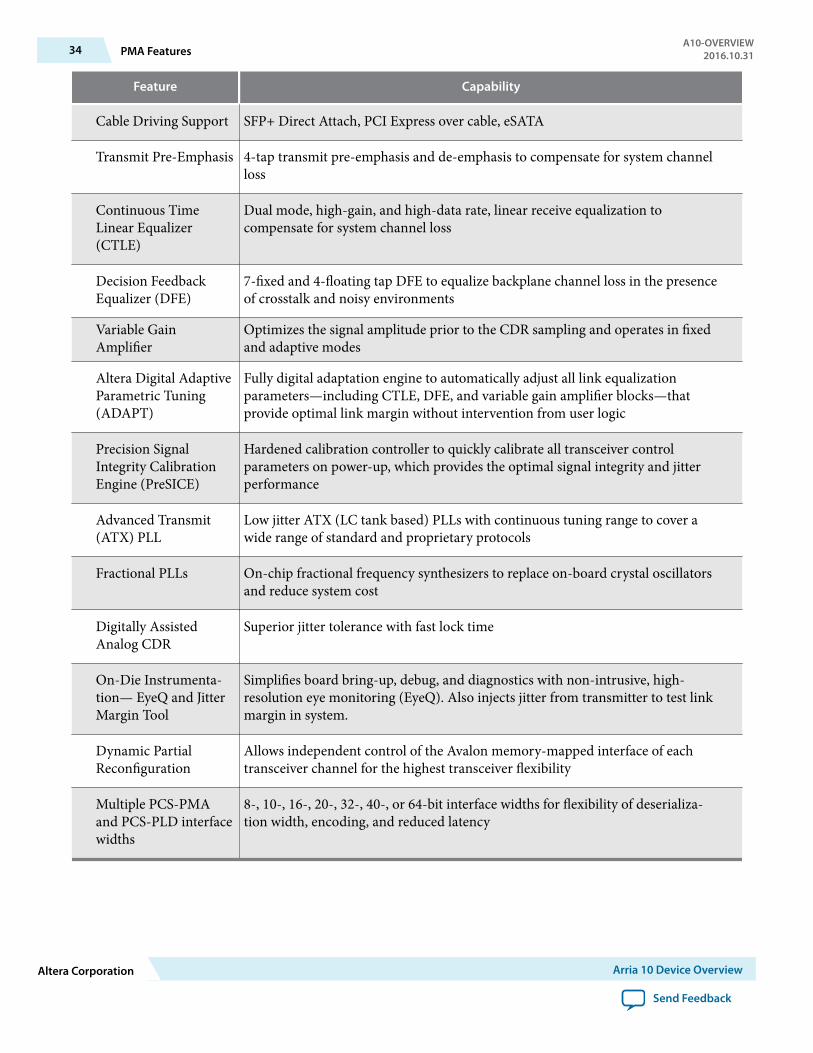
Feature Capability
Cable Driving Support SFP+ Direct Attach, PCI Express over cable, eSATA
Transmit Pre-Emphasis 4-tap transmit pre-emphasis and de-emphasis to compensate for system channelloss
Continuous TimeLinear Equalizer(CTLE)
Dual mode, high-gain, and high-data rate, linear receive equalization tocompensate for system channel loss
Decision FeedbackEqualizer (DFE)
7-fixed and 4-floating tap DFE to equalize backplane channel loss in the presenceof crosstalk and noisy environments
Variable GainAmplifier
Optimizes the signal amplitude prior to the CDR sampling and operates in fixedand adaptive modes
Altera Digital AdaptiveParametric Tuning(ADAPT)
Fully digital adaptation engine to automatically adjust all link equalizationparameters—including CTLE, DFE, and variable gain amplifier blocks—thatprovide optimal link margin without intervention from user logic
Precision SignalIntegrity CalibrationEngine (PreSICE)
Hardened calibration controller to quickly calibrate all transceiver controlparameters on power-up, which provides the optimal signal integrity and jitterperformance
Advanced Transmit(ATX) PLL
Low jitter ATX (LC tank based) PLLs with continuous tuning range to cover awide range of standard and proprietary protocols
Fractional PLLs On-chip fractional frequency synthesizers to replace on-board crystal oscillatorsand reduce system cost
Digitally AssistedAnalog CDR
Superior jitter tolerance with fast lock time
On-Die Instrumenta‐tion— EyeQ and JitterMargin Tool
Simplifies board bring-up, debug, and diagnostics with non-intrusive, high-resolution eye monitoring (EyeQ). Also injects jitter from transmitter to test linkmargin in system.
Dynamic PartialReconfiguration
Allows independent control of the Avalon memory-mapped interface of eachtransceiver channel for the highest transceiver flexibility
Multiple PCS-PMAand PCS-PLD interfacewidths
8-, 10-, 16-, 20-, 32-, 40-, or 64-bit interface widths for flexibility of deserializa‐tion width, encoding, and reduced latency
34 PMA FeaturesA10-OVERVIEW
2016.10.31
Altera Corporation Arria 10 Device Overview
Send Feedback
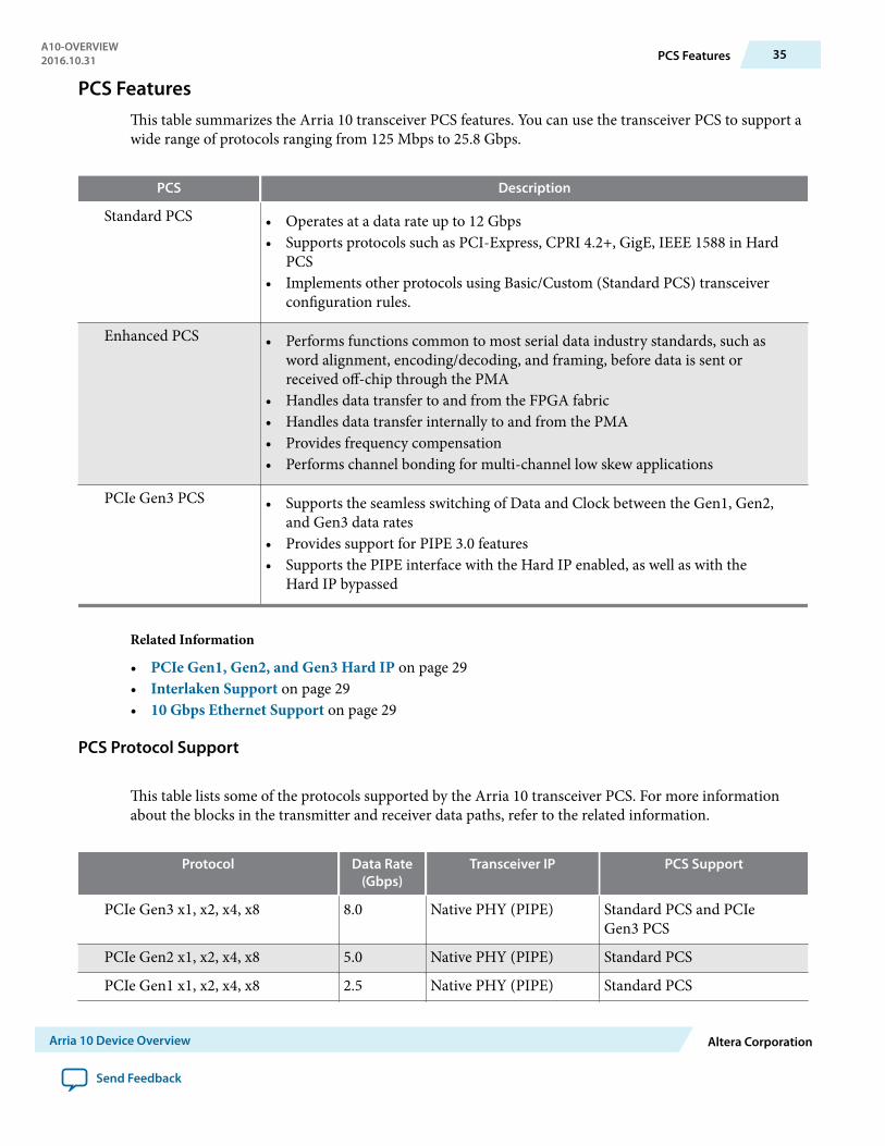
PCS FeaturesThis table summarizes the Arria 10 transceiver PCS features. You can use the transceiver PCS to support awide range of protocols ranging from 125 Mbps to 25.8 Gbps.
PCS Description
Standard PCS • Operates at a data rate up to 12 Gbps• Supports protocols such as PCI-Express, CPRI 4.2+, GigE, IEEE 1588 in Hard
PCS• Implements other protocols using Basic/Custom (Standard PCS) transceiver
configuration rules.
Enhanced PCS • Performs functions common to most serial data industry standards, such asword alignment, encoding/decoding, and framing, before data is sent orreceived off-chip through the PMA
• Handles data transfer to and from the FPGA fabric• Handles data transfer internally to and from the PMA• Provides frequency compensation• Performs channel bonding for multi-channel low skew applications
PCIe Gen3 PCS • Supports the seamless switching of Data and Clock between the Gen1, Gen2,and Gen3 data rates
• Provides support for PIPE 3.0 features• Supports the PIPE interface with the Hard IP enabled, as well as with the
Hard IP bypassed
Related Information
• PCIe Gen1, Gen2, and Gen3 Hard IP on page 29• Interlaken Support on page 29• 10 Gbps Ethernet Support on page 29
PCS Protocol Support
This table lists some of the protocols supported by the Arria 10 transceiver PCS. For more informationabout the blocks in the transmitter and receiver data paths, refer to the related information.
Protocol Data Rate(Gbps)
Transceiver IP PCS Support
PCIe Gen3 x1, x2, x4, x8 8.0 Native PHY (PIPE) Standard PCS and PCIeGen3 PCS
PCIe Gen2 x1, x2, x4, x8 5.0 Native PHY (PIPE) Standard PCS
PCIe Gen1 x1, x2, x4, x8 2.5 Native PHY (PIPE) Standard PCS
A10-OVERVIEW2016.10.31 PCS Features 35
Arria 10 Device Overview Altera Corporation
Send Feedback
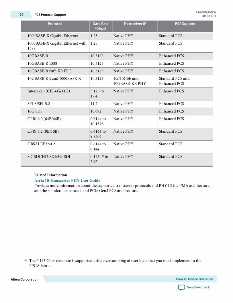
Protocol Data Rate(Gbps)
Transceiver IP PCS Support
1000BASE-X Gigabit Ethernet 1.25 Native PHY Standard PCS
1000BASE-X Gigabit Ethernet with1588
1.25 Native PHY Standard PCS
10GBASE-R 10.3125 Native PHY Enhanced PCS
10GBASE-R 1588 10.3125 Native PHY Enhanced PCS
10GBASE-R with KR FEC 10.3125 Native PHY Enhanced PCS
10GBASE-KR and 1000BASE-X 10.3125 1G/10GbE and10GBASE-KR PHY
Standard PCS andEnhanced PCS
Interlaken (CEI-6G/11G) 3.125 to17.4
Native PHY Enhanced PCS
SFI-S/SFI-5.2 11.2 Native PHY Enhanced PCS
10G SDI 10.692 Native PHY Enhanced PCS
CPRI 6.0 (64B/66B) 0.6144 to10.1376
Native PHY Enhanced PCS
CPRI 4.2 (8B/10B) 0.6144 to9.8304
Native PHY Standard PCS
OBSAI RP3 v4.2 0.6144 to6.144
Native PHY Standard PCS
SD-SDI/HD-SDI/3G-SDI 0.143(12) to2.97
Native PHY Standard PCS
Related InformationArria 10 Transceiver PHY User GuideProvides more information about the supported transceiver protocols and PHY IP, the PMA architecture,and the standard, enhanced, and PCIe Gen3 PCS architecture.
(12) The 0.143 Gbps data rate is supported using oversampling of user logic that you must implement in theFPGA fabric.
36 PCS Protocol SupportA10-OVERVIEW
2016.10.31
Altera Corporation Arria 10 Device Overview
Send Feedback
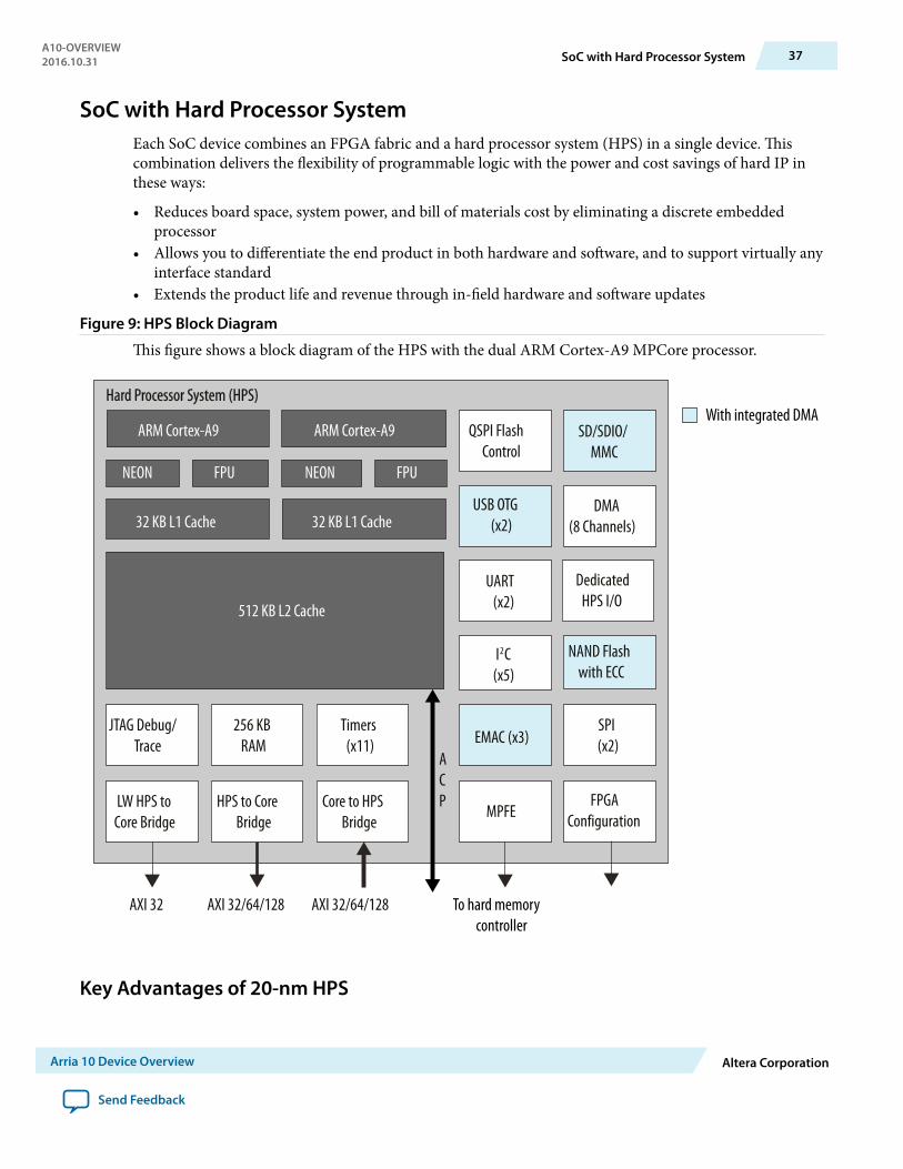
SoC with Hard Processor SystemEach SoC device combines an FPGA fabric and a hard processor system (HPS) in a single device. Thiscombination delivers the flexibility of programmable logic with the power and cost savings of hard IP inthese ways:
• Reduces board space, system power, and bill of materials cost by eliminating a discrete embeddedprocessor
• Allows you to differentiate the end product in both hardware and software, and to support virtually anyinterface standard
• Extends the product life and revenue through in-field hardware and software updates
Figure 9: HPS Block Diagram
This figure shows a block diagram of the HPS with the dual ARM Cortex-A9 MPCore processor.
ARM Cortex-A9 QSPI FlashControl
UART(x2)
ARM Cortex-A9
512 KB L2 Cache
EMAC (x3) JTAG Debug/
Trace
USB OTG(x2)
I2C(x5)
Hard Processor System (HPS)
256 KBRAM
Timers(x11)
LW HPS toCore Bridge
HPS to CoreBridge
Core to HPSBridge
MPFE
32 KB L1 Cache 32 KB L1 Cache
NEON FPU NEON FPU
AXI 32 AXI 32/64/128 AXI 32/64/128
ACP
SPI(x2)
NAND Flashwith ECC
With integrated DMA
To hard memorycontroller
SD/SDIO/MMC
DMA(8 Channels)
DedicatedHPS I/O
FPGAConfiguration
Key Advantages of 20-nm HPS
A10-OVERVIEW2016.10.31 SoC with Hard Processor System 37
Arria 10 Device Overview Altera Corporation
Send Feedback
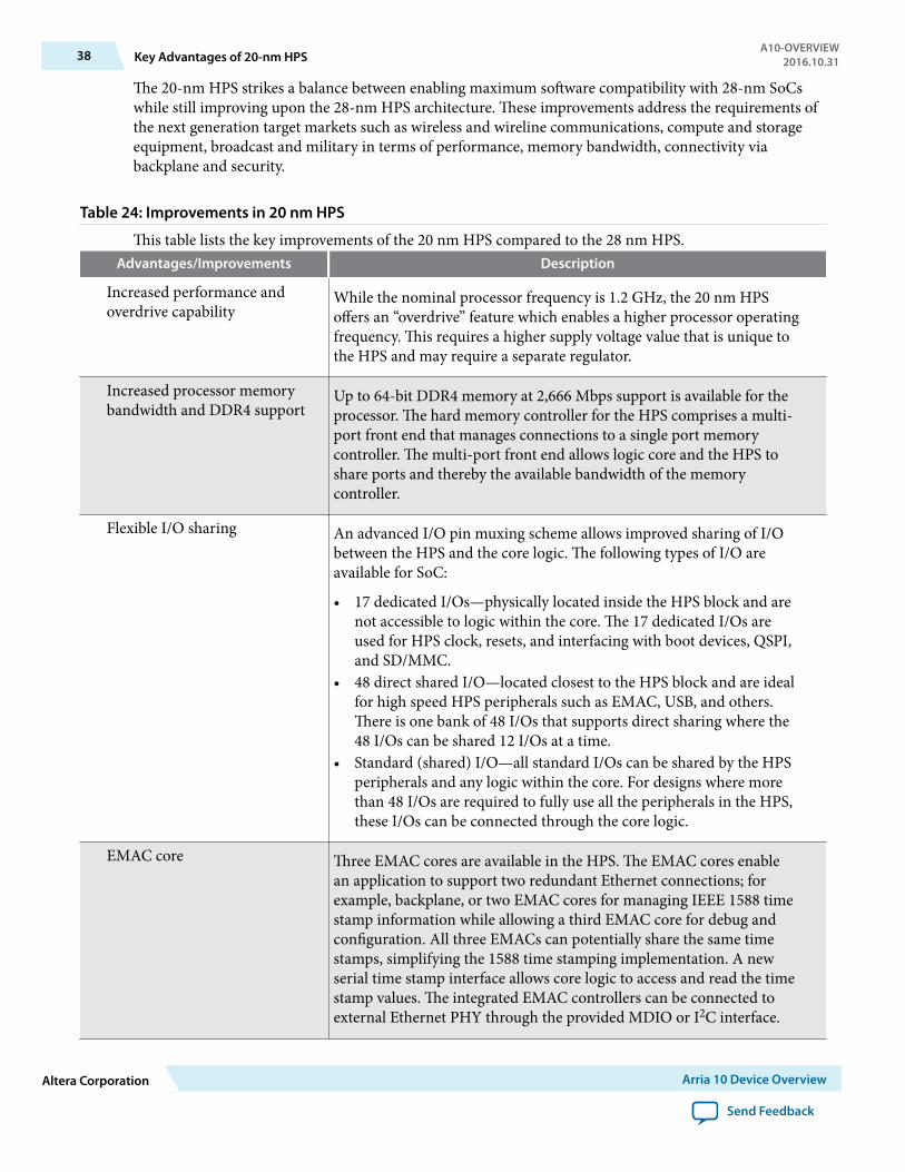
The 20-nm HPS strikes a balance between enabling maximum software compatibility with 28-nm SoCswhile still improving upon the 28-nm HPS architecture. These improvements address the requirements ofthe next generation target markets such as wireless and wireline communications, compute and storageequipment, broadcast and military in terms of performance, memory bandwidth, connectivity viabackplane and security.
Table 24: Improvements in 20 nm HPS
This table lists the key improvements of the 20 nm HPS compared to the 28 nm HPS.Advantages/Improvements Description
Increased performance andoverdrive capability
While the nominal processor frequency is 1.2 GHz, the 20 nm HPSoffers an “overdrive” feature which enables a higher processor operatingfrequency. This requires a higher supply voltage value that is unique tothe HPS and may require a separate regulator.
Increased processor memorybandwidth and DDR4 support
Up to 64-bit DDR4 memory at 2,666 Mbps support is available for theprocessor. The hard memory controller for the HPS comprises a multi-port front end that manages connections to a single port memorycontroller. The multi-port front end allows logic core and the HPS toshare ports and thereby the available bandwidth of the memorycontroller.
Flexible I/O sharing An advanced I/O pin muxing scheme allows improved sharing of I/Obetween the HPS and the core logic. The following types of I/O areavailable for SoC:
• 17 dedicated I/Os—physically located inside the HPS block and arenot accessible to logic within the core. The 17 dedicated I/Os areused for HPS clock, resets, and interfacing with boot devices, QSPI,and SD/MMC.
• 48 direct shared I/O—located closest to the HPS block and are idealfor high speed HPS peripherals such as EMAC, USB, and others.There is one bank of 48 I/Os that supports direct sharing where the48 I/Os can be shared 12 I/Os at a time.
• Standard (shared) I/O—all standard I/Os can be shared by the HPSperipherals and any logic within the core. For designs where morethan 48 I/Os are required to fully use all the peripherals in the HPS,these I/Os can be connected through the core logic.
EMAC core Three EMAC cores are available in the HPS. The EMAC cores enablean application to support two redundant Ethernet connections; forexample, backplane, or two EMAC cores for managing IEEE 1588 timestamp information while allowing a third EMAC core for debug andconfiguration. All three EMACs can potentially share the same timestamps, simplifying the 1588 time stamping implementation. A newserial time stamp interface allows core logic to access and read the timestamp values. The integrated EMAC controllers can be connected toexternal Ethernet PHY through the provided MDIO or I2C interface.
38 Key Advantages of 20-nm HPSA10-OVERVIEW
2016.10.31
Altera Corporation Arria 10 Device Overview
Send Feedback
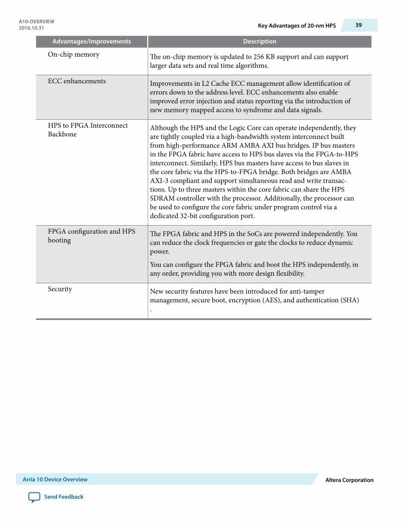
Advantages/Improvements Description
On-chip memory The on-chip memory is updated to 256 KB support and can supportlarger data sets and real time algorithms.
ECC enhancements Improvements in L2 Cache ECC management allow identification oferrors down to the address level. ECC enhancements also enableimproved error injection and status reporting via the introduction ofnew memory mapped access to syndrome and data signals.
HPS to FPGA InterconnectBackbone
Although the HPS and the Logic Core can operate independently, theyare tightly coupled via a high-bandwidth system interconnect builtfrom high-performance ARM AMBA AXI bus bridges. IP bus mastersin the FPGA fabric have access to HPS bus slaves via the FPGA-to-HPSinterconnect. Similarly, HPS bus masters have access to bus slaves inthe core fabric via the HPS-to-FPGA bridge. Both bridges are AMBAAXI-3 compliant and support simultaneous read and write transac‐tions. Up to three masters within the core fabric can share the HPSSDRAM controller with the processor. Additionally, the processor canbe used to configure the core fabric under program control via adedicated 32-bit configuration port.
FPGA configuration and HPSbooting
The FPGA fabric and HPS in the SoCs are powered independently. Youcan reduce the clock frequencies or gate the clocks to reduce dynamicpower.
You can configure the FPGA fabric and boot the HPS independently, inany order, providing you with more design flexibility.
Security New security features have been introduced for anti-tampermanagement, secure boot, encryption (AES), and authentication (SHA).
A10-OVERVIEW2016.10.31 Key Advantages of 20-nm HPS 39
Arria 10 Device Overview Altera Corporation
Send Feedback
Features of the HPSThe HPS has the following features:
• 1.2-GHz, dual-core ARM Cortex-A9 MPCore processor with up to 1.5-GHz via overdrive
• ARMv7-A architecture that runs 32-bit ARM instructions, 16-bit and 32-bit Thumb instructions,and 8-bit Java byte codes in Jazelle style
• Superscalar, variable length, out-of-order pipeline with dynamic branch prediction• Instruction Efficiency 2.5 MIPS/MHz, which provides total performance of 7500 MIPS at 1.5 GHz
• Each processor core includes:
• 32 KB of L1 instruction cache, 32 KB of L1 data cache• Single- and double-precision floating-point unit and NEON media engine• CoreSight debug and trace technology• Snoop Control Unit (SCU) and Acceleration Coherency Port (ACP)
• 512 KB of shared L2 cache• 256 KB of scratch RAM• Hard memory controller with support for DDR3, DDR4 and optional error correction code (ECC)
support• Multiport Front End (MPFE) Scheduler interface to the hard memory controller • 8-channel direct memory access (DMA) controller• QSPI flash controller with SIO, DIO, QIO SPI Flash support• NAND flash controller (ONFI 1.0 or later) with DMA and ECC support, updated to support 8 and 16-
bit Flash devices and new command DMA to offload CPU for fast power down recovery• Updated SD/SDIO/MMC controller to eMMC 4.5 with DMA with CE-ATA digital command support• 3 10/100/1000 Ethernet media access control (MAC) with DMA• 2 USB On-the-Go (OTG) controllers with DMA• 5 I2C controllers (3 can be used by EMAC for MIO to external PHY)• 2 UART 16550 Compatible controllers• 4 serial peripheral interfaces (SPI) (2 Master, 2 Slaves)• 62 programmable general-purpose I/Os, which includes 48 direct share I/Os that allows the HPS
peripherals to connect directly to the FPGA I/Os• 7 general-purpose timers• 4 watchdog timers• Anti-tamper, Secure Boot, Encryption (AES) and Authentication (SHA)
System Peripherals and Debug Access Port
Each Ethernet MAC, USB OTG, NAND flash controller, and SD/MMC controller module has anintegrated DMA controller. For modules without an integrated DMA controller, an additional DMAcontroller module provides up to eight channels of high-bandwidth data transfers. Peripherals thatcommunicate off-chip are multiplexed with other peripherals at the HPS pin level. This allows you tochoose which peripherals interface with other devices on your PCB.
The debug access port provides interfaces to industry standard JTAG debug probes and supports ARMCoreSight debug and core traces to facilitate software development.
HPS–FPGA AXI Bridges
40 Features of the HPSA10-OVERVIEW
2016.10.31
Altera Corporation Arria 10 Device Overview
Send Feedback
The HPS–FPGA bridges, which support the Advanced Microcontroller Bus Architecture (AMBA)Advanced eXtensible Interface (AXI™) specifications, consist of the following bridges:
• FPGA-to-HPS AMBA AXI bridge—a high-performance bus supporting 32, 64, and 128 bit data widthsthat allows the FPGA fabric to issue transactions to slaves in the HPS.
• HPS-to-FPGA Avalon/AMBA AXI bridge—a high-performance bus supporting 32, 64, and 128 bitdata widths that allows the HPS to issue transactions to slaves in the FPGA fabric.
• Lightweight HPS-to-FPGA AXI bridge—a lower latency 32 bit width bus that allows the HPS to issuetransactions to soft peripherals in the FPGA fabric. This bridge is primarily used for control and statusregister (CSR) accesses to peripherals in the FPGA fabric.
The HPS–FPGA AXI bridges allow masters in the FPGA fabric to communicate with slaves in the HPSlogic, and vice versa. For example, the HPS-to-FPGA AXI bridge allows you to share memories instanti‐ated in the FPGA fabric with one or both microprocessors in the HPS, while the FPGA-to-HPS AXIbridge allows logic in the FPGA fabric to access the memory and peripherals in the HPS.
Each HPS–FPGA bridge also provides asynchronous clock crossing for data transferred between theFPGA fabric and the HPS.
HPS SDRAM Controller Subsystem
The HPS SDRAM controller subsystem contains a multiport SDRAM controller and DDR PHY that areshared between the FPGA fabric (through the FPGA-to-HPS SDRAM interface), the level 2 (L2) cache,and the level 3 (L3) system interconnect. The FPGA-to-HPS SDRAM interface supports AMBA AXI andAvalon® Memory-Mapped (Avalon-MM) interface standards, and provides up to six individual ports foraccess by masters implemented in the FPGA fabric.
The HPS SDRAM controller supports up to 3 masters (command ports), 3x 64-bit read data ports and 3x64-bit write data ports.
To maximize memory performance, the SDRAM controller subsystem supports command and datareordering, deficit round-robin arbitration with aging, and high-priority bypass features.
FPGA Configuration and HPS BootingThe FPGA fabric and HPS in the SoC FPGA must be powered at the same time. You can reduce the clockfrequencies or gate the clocks to reduce dynamic power.
Once powered, the FPGA fabric and HPS can be configured independently thus providing you with moredesign flexibility:
• You can boot the HPS independently. After the HPS is running, the HPS can fully or partiallyreconfigure the FPGA fabric at any time under software control. The HPS can also configure otherFPGAs on the board through the FPGA configuration controller.
• Configure the FPGA fabric first, and then boot the HPS from memory accessible to the FPGA fabric.
Hardware and Software Development
For hardware development, you can configure the HPS and connect your soft logic in the FPGA fabric tothe HPS interfaces using the Qsys system integration tool in the Quartus Prime software.
For software development, the ARM-based SoC FPGA devices inherit the rich software developmentecosystem available for the ARM Cortex-A9 MPCore processor. The software development process for
A10-OVERVIEW2016.10.31 HPS SDRAM Controller Subsystem 41
Arria 10 Device Overview Altera Corporation
Send Feedback
Altera SoC FPGAs follows the same steps as those for other SoC devices from other manufacturers.Support for Linux, VxWorks®, and other operating systems will be available for the SoC FPGAs. For moreinformation on the operating systems support availability, contact the Altera sales team.
You can begin device-specific firmware and software development on the Altera SoC FPGA Virtual Target.The Virtual Target is a fast PC-based functional simulation of a target development system—a model of acomplete development board. The Virtual Target enables the development of device-specific productionsoftware that can run unmodified on actual hardware.
Dynamic and Partial ReconfigurationThe Arria 10 devices support dynamic and partial reconfiguration. You can use dynamic and partialreconfiguration simultaneously to enable seamless reconfiguration of both the device core andtransceivers.
Dynamic Reconfiguration
You can reconfigure the PMA and PCS blocks while the device continues to operate. This feature allowsyou to change the data rates, protocol, and analog settings of a channel in a transceiver bank withoutaffecting on-going data transfer in other transceiver banks. This feature is ideal for applications thatrequire dynamic multiprotocol or multirate support.
Partial ReconfigurationUsing partial reconfiguration, you can reconfigure some parts of the device while keeping the device inoperation.
Instead of placing all device functions in the FPGA fabric, you can store some functions that do not runsimultaneously in external memory and load them only when required. This capability increases theeffective logic density of the device, and lowers cost and power consumption.
In the Altera® solution, you do not have to worry about intricate device architecture to perform a partialreconfiguration. The partial reconfiguration capability is built into the Quartus Prime design software,making such time-intensive task simple.
Arria 10 devices support partial reconfiguration in the following configuration options:
• Using an internal host:
• All supported configuration modes where the FPGA has access to external memory devices such asserial and parallel flash memory.
• Configuration via Protocol [CvP (PCIe)]• Using an external host—passive serial (PS), fast passive parallel (FPP) x8, FPP x16, and FPP x32 I/O
interface.
Enhanced Configuration and Configuration via Protocol
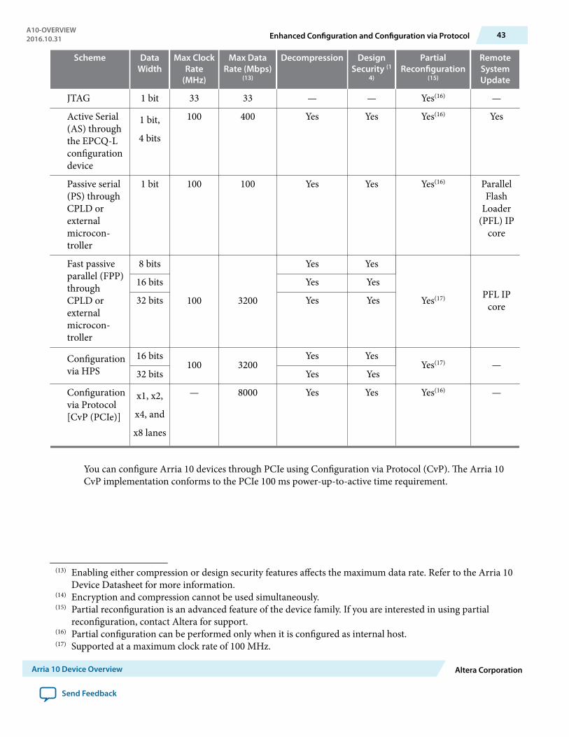
Table 25: Configuration Schemes and Features of Arria 10 Devices
Arria 10 devices support 1.8 V programming voltage and several configuration schemes.
42 Dynamic and Partial ReconfigurationA10-OVERVIEW
2016.10.31
Altera Corporation Arria 10 Device Overview
Send Feedback
Scheme DataWidth
Max ClockRate
(MHz)
Max DataRate (Mbps)
(13)
Decompression DesignSecurity (1
4)
PartialReconfiguration
(15)
RemoteSystemUpdate
JTAG 1 bit 33 33 — — Yes(16) —
Active Serial(AS) throughthe EPCQ-Lconfigurationdevice
1 bit,
4 bits
100 400 Yes Yes Yes(16) Yes
Passive serial(PS) throughCPLD orexternalmicrocon‐troller
1 bit 100 100 Yes Yes Yes(16) ParallelFlash
Loader(PFL) IP
core
Fast passiveparallel (FPP)throughCPLD orexternalmicrocon‐troller
8 bits
100 3200
Yes Yes
Yes(17) PFL IPcore
16 bits Yes Yes
32 bits Yes Yes
Configurationvia HPS
16 bits100 3200
Yes YesYes(17) —
32 bits Yes Yes
Configurationvia Protocol[CvP (PCIe)]
x1, x2,
x4, and
x8 lanes
— 8000 Yes Yes Yes(16) —
You can configure Arria 10 devices through PCIe using Configuration via Protocol (CvP). The Arria 10CvP implementation conforms to the PCIe 100 ms power-up-to-active time requirement.
(13) Enabling either compression or design security features affects the maximum data rate. Refer to the Arria 10Device Datasheet for more information.
(14) Encryption and compression cannot be used simultaneously.(15) Partial reconfiguration is an advanced feature of the device family. If you are interested in using partial
reconfiguration, contact Altera for support.(16) Partial configuration can be performed only when it is configured as internal host.(17) Supported at a maximum clock rate of 100 MHz.
A10-OVERVIEW2016.10.31 Enhanced Configuration and Configuration via Protocol 43
Arria 10 Device Overview Altera Corporation
Send Feedback
SEU Error Detection and CorrectionArria 10 devices offer robust and easy-to-use single-event upset (SEU) error detection and correctioncircuitry.
The detection and correction circuitry includes protection for Configuration RAM (CRAM) programmingbits and user memories. The CRAM is protected by a continuously running CRC error detection circuitwith integrated ECC that automatically corrects one or two errors and detects higher order multi-biterrors. When more than two errors occur, correction is available through reloading of the core program‐ming file, providing a complete design refresh while the FPGA continues to operate.
The physical layout of the Arria 10 CRAM array is optimized to make the majority of multi-bit upsetsappear as independent single-bit or double-bit errors which are automatically corrected by the integratedCRAM ECC circuitry. In addition to the CRAM protection, the M20K memory blocks also includeintegrated ECC circuitry and are layout-optimized for error detection and correction. The MLAB does nothave ECC.
Power ManagementArria 10 devices leverage the advanced 20 nm process technology, a low 0.9 V core power supply, anenhanced core architecture, and several optional power reduction techniques to reduce total powerconsumption by as much as 40% compared to Arria V devices and as much as 60% compared to Stratix Vdevices.
The optional power reduction techniques in Arria 10 devices include:
• SmartVID—a code is programmed into each device during manufacturing that allows a smartregulator to operate the device at lower core VCC while maintaining performance
• Programmable Power Technology—non-critical timing paths are identified by the Quartus Primesoftware and the logic in these paths is biased for low power instead of high performance
• Low Static Power Options—devices are available with either standard static power or low static powerwhile maintaining performance
Furthermore, Arria 10 devices feature Altera’s industry-leading low power transceivers and include anumber of hard IP blocks that not only reduce logic resources but also deliver substantial power savingscompared to soft implementations. In general, hard IP blocks consume up to 90% less power than theequivalent soft logic implementations.
Incremental CompilationThe Quartus Prime software incremental compilation feature reduces compilation time and helps preserveperformance to ease timing closure. The incremental compilation feature enables the partialreconfiguration flow for Arria 10 devices.
Incremental compilation supports top-down, bottom-up, and team-based design flows. This featurefacilitates modular, hierarchical, and team-based design flows where different designers compile theirrespective design sections in parallel. Furthermore, different designers or IP providers can develop andoptimize different blocks of the design independently. These blocks can then be imported into the top levelproject.
44 SEU Error Detection and CorrectionA10-OVERVIEW
2016.10.31
Altera Corporation Arria 10 Device Overview
Send Feedback
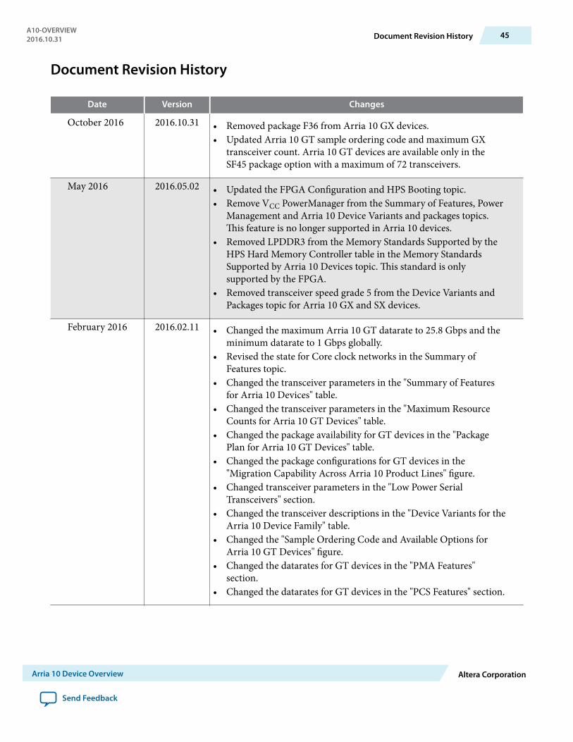
Document Revision History
Date Version Changes
October 2016 2016.10.31 • Removed package F36 from Arria 10 GX devices.• Updated Arria 10 GT sample ordering code and maximum GX
transceiver count. Arria 10 GT devices are available only in theSF45 package option with a maximum of 72 transceivers.
May 2016 2016.05.02 • Updated the FPGA Configuration and HPS Booting topic.• Remove VCC PowerManager from the Summary of Features, Power
Management and Arria 10 Device Variants and packages topics.This feature is no longer supported in Arria 10 devices.
• Removed LPDDR3 from the Memory Standards Supported by theHPS Hard Memory Controller table in the Memory StandardsSupported by Arria 10 Devices topic. This standard is onlysupported by the FPGA.
• Removed transceiver speed grade 5 from the Device Variants andPackages topic for Arria 10 GX and SX devices.
February 2016 2016.02.11 • Changed the maximum Arria 10 GT datarate to 25.8 Gbps and theminimum datarate to 1 Gbps globally.
• Revised the state for Core clock networks in the Summary ofFeatures topic.
• Changed the transceiver parameters in the "Summary of Featuresfor Arria 10 Devices" table.
• Changed the transceiver parameters in the "Maximum ResourceCounts for Arria 10 GT Devices" table.
• Changed the package availability for GT devices in the "PackagePlan for Arria 10 GT Devices" table.
• Changed the package configurations for GT devices in the"Migration Capability Across Arria 10 Product Lines" figure.
• Changed transceiver parameters in the "Low Power SerialTransceivers" section.
• Changed the transceiver descriptions in the "Device Variants for theArria 10 Device Family" table.
• Changed the "Sample Ordering Code and Available Options forArria 10 GT Devices" figure.
• Changed the datarates for GT devices in the "PMA Features"section.
• Changed the datarates for GT devices in the "PCS Features" section.
A10-OVERVIEW2016.10.31 Document Revision History 45
Arria 10 Device Overview Altera Corporation
Send Feedback
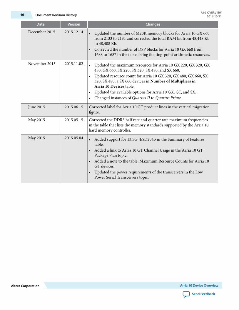
Date Version Changes
December 2015 2015.12.14 • Updated the number of M20K memory blocks for Arria 10 GX 660from 2133 to 2131 and corrected the total RAM bit from 48,448 Kbto 48,408 Kb.
• Corrected the number of DSP blocks for Arria 10 GX 660 from1688 to 1687 in the table listing floating-point arithmetic resources.
November 2015 2015.11.02 • Updated the maximum resources for Arria 10 GX 220, GX 320, GX480, GX 660, SX 220, SX 320, SX 480, and SX 660.
• Updated resource count for Arria 10 GX 320, GX 480, GX 660, SX320, SX 480, a SX 660 devices in Number of Multipliers inArria 10 Devices table.
• Updated the available options for Arria 10 GX, GT, and SX.• Changed instances of Quartus II to Quartus Prime.
June 2015 2015.06.15 Corrected label for Arria 10 GT product lines in the vertical migrationfigure.
May 2015 2015.05.15 Corrected the DDR3 half rate and quarter rate maximum frequenciesin the table that lists the memory standards supported by the Arria 10hard memory controller.
May 2015 2015.05.04 • Added support for 13.5G JESD204b in the Summary of Featurestable.
• Added a link to Arria 10 GT Channel Usage in the Arria 10 GTPackage Plan topic.
• Added a note to the table, Maximum Resource Counts for Arria 10GT devices.
• Updated the power requirements of the transceivers in the LowPower Serial Transceivers topic.
46 Document Revision HistoryA10-OVERVIEW
2016.10.31
Altera Corporation Arria 10 Device Overview
Send Feedback
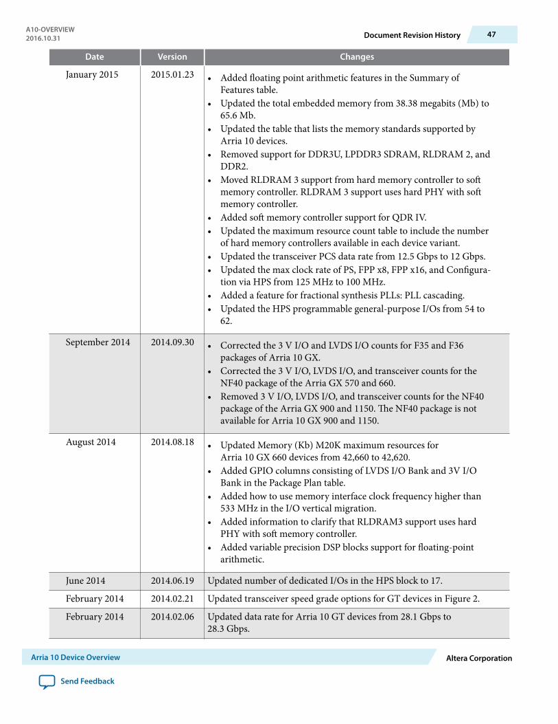
Date Version Changes
January 2015 2015.01.23 • Added floating point arithmetic features in the Summary ofFeatures table.
• Updated the total embedded memory from 38.38 megabits (Mb) to65.6 Mb.
• Updated the table that lists the memory standards supported byArria 10 devices.
• Removed support for DDR3U, LPDDR3 SDRAM, RLDRAM 2, andDDR2.
• Moved RLDRAM 3 support from hard memory controller to softmemory controller. RLDRAM 3 support uses hard PHY with softmemory controller.
• Added soft memory controller support for QDR IV.• Updated the maximum resource count table to include the number
of hard memory controllers available in each device variant.• Updated the transceiver PCS data rate from 12.5 Gbps to 12 Gbps.• Updated the max clock rate of PS, FPP x8, FPP x16, and Configura‐
tion via HPS from 125 MHz to 100 MHz.• Added a feature for fractional synthesis PLLs: PLL cascading.• Updated the HPS programmable general-purpose I/Os from 54 to
62.
September 2014 2014.09.30 • Corrected the 3 V I/O and LVDS I/O counts for F35 and F36packages of Arria 10 GX.
• Corrected the 3 V I/O, LVDS I/O, and transceiver counts for theNF40 package of the Arria GX 570 and 660.
• Removed 3 V I/O, LVDS I/O, and transceiver counts for the NF40package of the Arria GX 900 and 1150. The NF40 package is notavailable for Arria 10 GX 900 and 1150.
August 2014 2014.08.18 • Updated Memory (Kb) M20K maximum resources forArria 10 GX 660 devices from 42,660 to 42,620.
• Added GPIO columns consisting of LVDS I/O Bank and 3V I/OBank in the Package Plan table.
• Added how to use memory interface clock frequency higher than533 MHz in the I/O vertical migration.
• Added information to clarify that RLDRAM3 support uses hardPHY with soft memory controller.
• Added variable precision DSP blocks support for floating-pointarithmetic.
June 2014 2014.06.19 Updated number of dedicated I/Os in the HPS block to 17.
February 2014 2014.02.21 Updated transceiver speed grade options for GT devices in Figure 2.
February 2014 2014.02.06 Updated data rate for Arria 10 GT devices from 28.1 Gbps to28.3 Gbps.
A10-OVERVIEW2016.10.31 Document Revision History 47
Arria 10 Device Overview Altera Corporation
Send Feedback
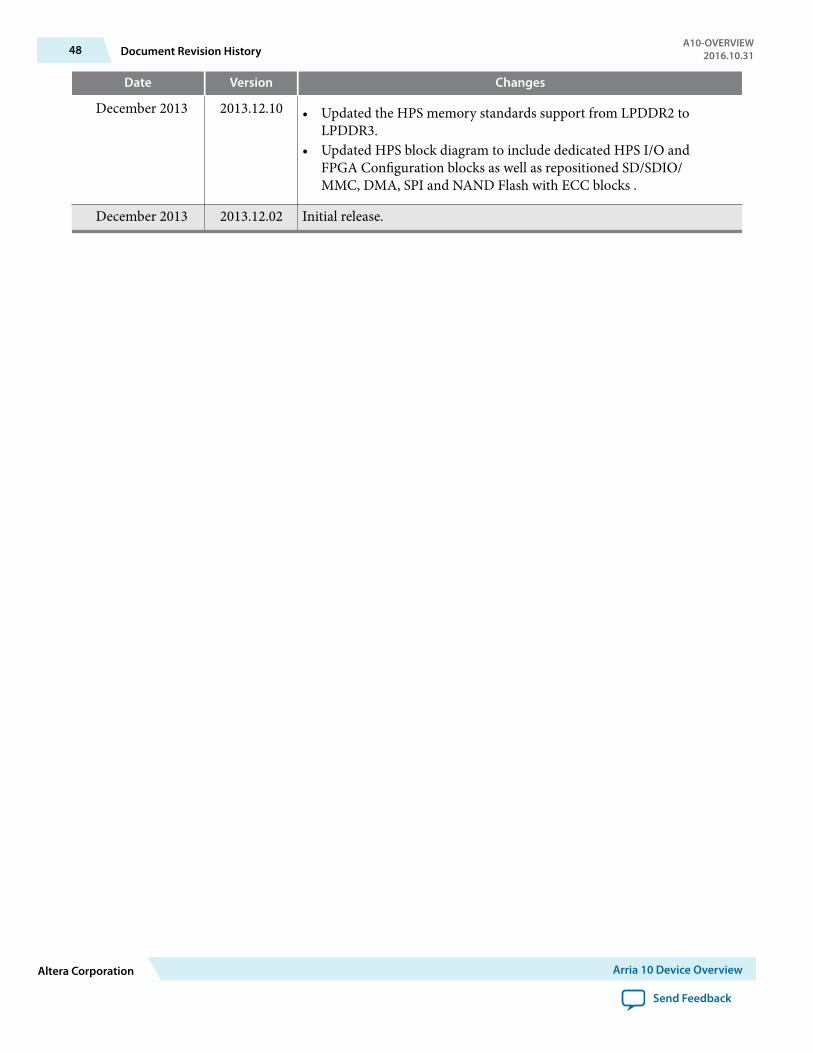
Date Version Changes
December 2013 2013.12.10 • Updated the HPS memory standards support from LPDDR2 toLPDDR3.
• Updated HPS block diagram to include dedicated HPS I/O andFPGA Configuration blocks as well as repositioned SD/SDIO/MMC, DMA, SPI and NAND Flash with ECC blocks .
December 2013 2013.12.02 Initial release.
48 Document Revision HistoryA10-OVERVIEW
2016.10.31
Altera Corporation Arria 10 Device Overview
Send Feedback
Mouser Electronics
Authorized Distributor
Click to View Pricing, Inventory, Delivery & Lifecycle Information: Altera:
10AT115N2F40E2SGES 10AS066H3F34I3SGES 10AX115N3F40I3SGES 10AX115S4F45I4SGES
10AT115N3F40E3SGES 10AX115R4F40I4SGES 10AX066H2F34I2SGES 10AS066H4F34I4SGES
10AX115N2F40I2SGES 10AX066K4F35I4SGES 10AT115U3F45E3SGES 10AX066H4F34I4SGES
10AS066K3F35I3SGES 10AX115R2F40I2SGES 10AX115U1F45I2SGES 10AS066H2F34I2SGES
10AX115S3F45I3SGES 10AX115U2F45I2SGES 10AX115U3F45I3SGES 10AX115R3F40I3SGES
10AX066K2F35I2SGES 10AX115N1F40I2SGES 10AX066H3F34I3SGES 10AT115U2F45E2SGES
10AS066K2F35I2SGES 10AX115S1F45I2SGES 10AX115N4F40I4SGES 10AX115S2F45I2SGES
10AX115U4F45I4SGES 10AT115U4F45E4SGES 10AS066K4F35I4SGES 10AT115N4F40E4SGES
10AX066K3F35I3SGES 10AT115N3F40E2SGES 10AX115N3F45I2SGES 10AX066H3F34I2SGES
10AX115S4F45I3SGES 10AS066K3F35I2SGES 10AS066H4F34I3SGES 10AX115U4F45I3SGES
10AX115N3F40I2SGES 10AX066K3F35I2SGES 10AX115S3F45I2SGES 10AT115N4F40E3SGES
10AX066K4F35I3SGES 10AX115R4F40I3SGES 10AS066K4F35I3SGES 10AS066H3F34I2SGES
10AT115U3F45E2SGES 10AX115U3F45I2SGES 10AX115R3F40I2SGES 10AT115U4F45E3SGES
10AX115N4F45I3SGES 10AX115N4F40I3SGES 10AX066H4F34I3SGES 10AS066N4F40I3SGES
10AX066N4F40I3SGES 10AX115H3F34I2SGES 10AX115H4F34I3SGES 10AX115N2F45I2SGES
10AS066N2F40I2SGES 10AS048K2F35I2SG 10AS032H4F35E3LG 10AX048E3F29I2LG 10AX027H1F34E1SG
10AX016E4F27I3LG 10AS032H4F34I3SG 10AS022C4U19E3LG 10AS022E3F29I2LG 10AX048K4F35I3LG
10AS048H2F34I2LG 10AS016C3U19I2SG 10AS032E4F29E3SG 10AS032H4F35I3SG 10AX032H2F35I1SG
10AX022E3F29E1SG 10AX048E2F29I2LG 10AX022C4U19E3LG 10AS016E3F27I2LG 10AS032E4F29I3SG
10AS027E3F27I2LG 10AX022C3U19I2SG 10AX027E1F27E1SG 10AX022E4F29I3LG 10AS027H4F35I3LG
10AX027H3F35E2LG 10AS027H2F34E2SG 10AX022E4F27E3SG 10AS032E2F29I2LG 10AS032E4F29I3LG
10AS048K2F35I2LG 10AX016E4F27E3SG 10AS027H3F34E2LG 10AS027E4F27E3SG 10AS027E2F27I2LG
10AS048E3F29I2LG 10AS027E4F27I3LG 10AX022E3F29I1SG 10AS048E2F29I2SG 10AX027E4F29I3SG