Embed Size (px)
Citation preview

As you wait for the lab to start : Reserve seats for your partners
Digital Logic and
State Machine Design
CS CS 22042204CS CS 22042204
Lab 4
Experiment 1
Spring Spring 20142014Spring Spring 20142014

Experiment 1 Lab 4 Outline Presentation
Using A Brief Look at Semiconductor Technology Component selection for a new chip and a new PCB Semiconductor technology overview
• Gates, switches and digital electronic circuits• Complementary Metal Oxide Semiconductor (CMOS) overview• Transistor-Transistor Logic (TTL) overview
Using Term Project (pages 20 - 21) Analysis of the term project
• Digital Systems• Analysis of Block 3 of the term project
Using Term Project Design Checks Digital Design Conventions
Individual work Experiment 1 is over three weeks : Labs 3, 4 and 5
Develop a 4-bit 2-to-1 MUX of Block 2• By using Handout 3 distributed in class
New handout Term Project Design Checks
Experiment 1 Lab 4CS 2204 Spring 2014 Page 2

Presentation Xilinx Project Development Steps
Develop the schematic Design the schematic
• Place the components and wires Do a schematic check Test the schematic via logic simulations
Do a Xilinx IMPLEMENTATION It maps the components to the CLBs of the chip
• Do timing simulations to test the schematic It generates the bit file
Download the bit file to the FPGA and test the design on the board
It programs the chip
Experiment 1 Lab 4CS 2204 Spring 2014 Page 3
Today’swork
What are thesecomponents ?

Developing a digital product A new chip
Which gates & FFs and how many is determined by Available components of technology chosen Besides the major operations and speed, cost, power, etc.
design goals of the digital product FPGAs are used to test the new chip
A new PCB Which chips and how many is determined by
Available chips of technology chosen Besides the major operations and speed, cost, power, etc.
design goals of the digital product
Experiment 1 Lab 4CS 2204 Spring 2014 Page 4

Developing a digital product A new chip
We will try to use high density components as much as possible
We will try not to use low-density components (gates and flip-flops)
We will work on chip design in the classroom and in the lab
Lectures, homework assignments, exams and labs
Experiment 1 Lab 4CS 2204 Spring 2014 Page 5

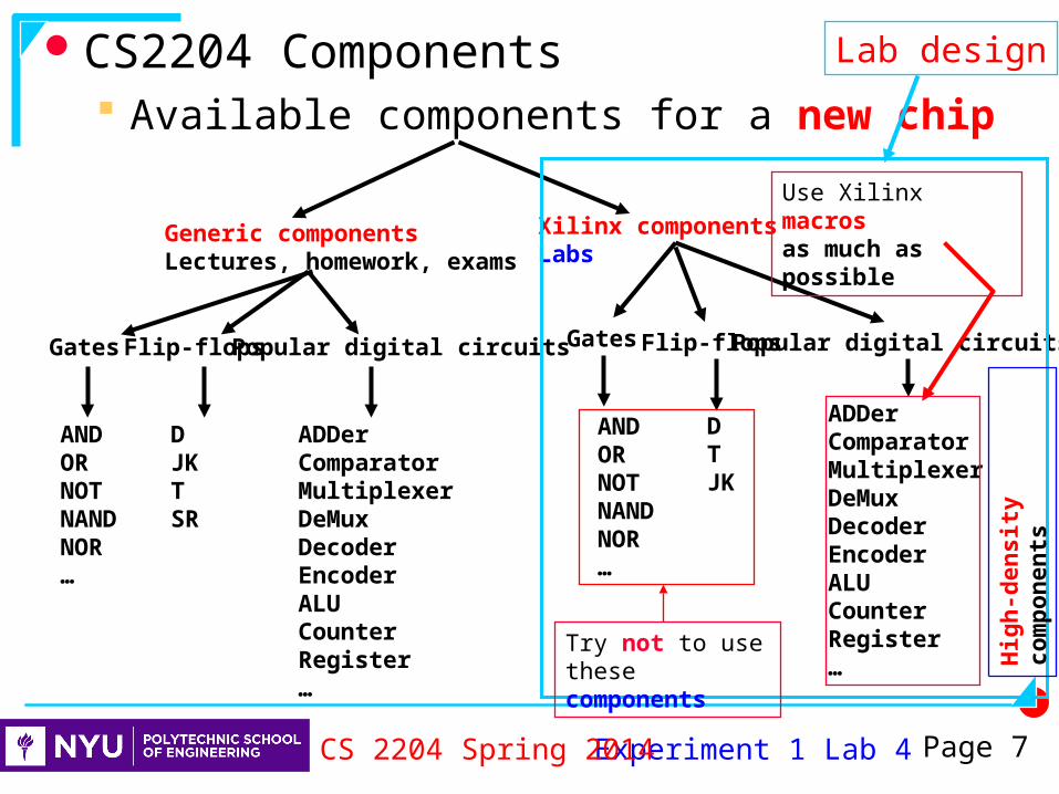
CS2204 Components Available components for a new chip
Experiment 1 Lab 4CS 2204 Spring 2014 Page 6
Generic componentsLectures, homework, exams
Xilinx components Labs
Gates Flip-flopsPopular digital circuits Gates Flip-flops Popular digital circuits
ANDORNOTNANDNOR…
DJKTSR…
ADDerComparatorMultiplexerDeMuxDecoderEncoderALUCounterRegister…
ANDORNOTNANDNOR…
DTJK
ADDerComparatorMultiplexerDeMuxDecoderEncoderALUCounterRegister…
Use these as much as possible
To save time,space, power.weight,… H
igh
-den
sit
y
com
pon
en
ts
CS2204 Components Available components for a new chip
Experiment 1 Lab 4CS 2204 Spring 2014 Page 7
Generic componentsLectures, homework, exams
Xilinx componentsLabs
Gates Flip-flopsPopular digital circuits Gates Flip-flopsPopular digital circuits
ANDORNOTNANDNOR…
DJKTSR
ADDerComparatorMultiplexerDeMuxDecoderEncoderALUCounterRegister…
ADDerComparatorMultiplexerDeMuxDecoderEncoderALUCounterRegister…
Lab design
Use Xilinx macros as much as possible
ANDORNOTNANDNOR…
DTJK
Try not to use these components
Hig
h-d
en
sit
y
com
pon
en
ts

Developing a digital product A new PCB
We will try to use high density chips (MSI, LSI, VLSI, ULSI) as much as possible
We will try not to use low-density chips (SSI)
We will work on PCB design in the classroom
Lectures, homework assignments and exams
Experiment 1 Lab 4CS 2204 Spring 2014 Page 8

CS2204 components Available chips for a new PCB
Experiment 1 Lab 4CS 2204 Spring 2014 Page 9
Generic chipsLectures, homework, examsTTL LS chips
Lectures, homework, exams
Gates Flip-flopsPopular digital circuitsGates Flip-flops Popular digital circuits
ANDORNOTNANDNOR…
DJKTSR…
ADDerComparatorMultiplexerDeMuxDecoderEncoderALUCounterRegister…
ANDORNOTNANDNOR…
DJK
ADDerComparatorMultiplexerDeMuxDecoderEncoderALUCounterRegister…
Use these as much as possible
To save time,space, power.weight,… H
igh
-den
sit
y
ch
ips

CS2204 components Available chips for a new PCB
Experiment 1 Lab 4CS 2204 Spring 2014 Page 10
Generic chipsLectures, homework, exams
TTL LS chipsLectures, homework, exams
Gates Flip-flopsPopular digital circuitsGates Flip-flops Popular digital circuits
ANDORNOTNANDNOR…
DJKTSR…
ADDerComparatorMultiplexerDeMuxDecoderEncoderALUCounterRegister…
ANDORNOTNANDNOR…
DJK
ADDerComparatorMultiplexerDeMuxDecoderEncoderALUCounterRegister…
Use higher density chips (MSI, LSI,…) as much as possible
Try not to use these SSI chips
Hig
h-d
en
sit
y
ch
ips
MS
I, L
SI
ch
ips

Digital circuits consist of gates and FFs FFs consist of gates
Digital circuits consist of gates ! Gates are on chips !
Chips are on PCBs
Experiment 1 Lab 4CS 2204 Spring 2014 Page 11
D FF
D FF implementationvia gates
From ON Semiconductor LS TTL Data Manual

Gates are implemented by electronic components : Transistors, resistors, diodes, capacitors,…
Experiment 1 Lab 4CS 2204 Spring 2014 Page 12
From ON Semiconductor LS TTL Data Manual
74LS00Quad2-inputTTLNANDGatechip
TTL 2-inputNAND gate implementationvia electroniccomponents
CMOS 2-inputNAND gate implementationvia electroniccomponents
NAND

Most Common Voltages for Logic Values Logic 1 is +5v Logic 0 is 0v The terminology
+5v VCC 0v GND (Ground)
Xilinx Devices for voltages
Experiment 1 Lab 4CS 2204 Spring 2014 Page 13
TTL 2-input NAND gateON SemiconductorLS TTL Data Manual
VCC and GND are on theXilinx component list
CMOS 2-inputNAND gate implementationvia electroniccomponents
2-input NAND gate

Transistors are the Main Electronic Component Transistors are used as switches to implement
gates A switch is open or closed based on the control input
value :
Open when control is 0 :
Closed when control is 1
The speed of switches determines the speed of the electronic circuit, therefore, the gate
Experiment 1 Lab 4CS 2204 Spring 2014 Page 14
0
1 0
1
1 1

Implementing AND gates
Implemented by two switches connected in series
Experiment 1 Lab 4CS 2204 Spring 2014 Page 15
ANDk
mk.m
AND gate
k.m
k m
11

Implementing OR gates
Implemented by two switches connected in parallel
Experiment 1 Lab 4CS 2204 Spring 2014 Page 16
ORk
m k + m
OR gate
k
1
m
k + m

Implementing NOT gates
Implemented by one switch
Experiment 1 Lab 4CS 2204 Spring 2014 Page 17
NOTk k
NOT gate (inverter)
k
1 1

2-to-1 MUX Implementation
Experiment 1 Lab 4CS 2204 Spring 2014 Page 18
AND
AND
OR
NOTa
b
a
cy(a, b, c) =y(a, b, c) = a.b + a.ca.b + a.c
a c
a b
1 y(a, b, c) =y(a, b, c) = a.b + a.ca.b + a.c
A switching networkimplementinga gate network

The Gate Implementation Implementing gates is more complex than just connecting
switches (transistors) in series/parallel A 2-input NAND gate implementation
Resistors, diodes, etc. are used for reliable operation with TTL technology
• Five transistors : Q1 – Q5, six diodes : D1 – D6 and seven resistors Multiple transistors are used for reliable operation with CMOS
technology • A 2-input NAND gate implementation• Four transistors
Experiment 1 Lab 4CS 2204 Spring 2014 Page 19
CMOS 2-inputNAND gate implementationvia electroniccomponents
NAND
TTL 2-input NAND gateON SemiconductorLS TTL Data Manual

Electronic Components on the Chip All electronic components are placed in
the die area
Experiment 1 Lab 4CS 2204 Spring 2014 Page 20
A chip
Die
The die of chip : area containing transistors, resistors, diodes,…
There are more than 225 million transistors on dieIntel Pentium 4 die
www.intel.com

Die Fabrication Today Dice for the same chip type are placed on a
wafer
Experiment 1 Lab 4CS 2204 Spring 2014 Page 21
Intel Pentium4 wafer
Intel Pentium 4 chip
Die
Intel Pentium 4 die
From : Intel

Gates have features Speed, Cost, Power, Size,…
Transistors, resistors,.. have features (device characteristics) Speed, cost, power, size,.. Device characteristics are determined by
The substance used for chips Silicon, Silicon Germanium, Gallium Arsenide
The transistor type Unipolar, bipolar
Electronic (transistor) circuits that form the gates CMOS, BiCMOS, TTL, ECL,…
Experiment 1 Lab 4CS 2204 Spring 2014 Page 22
Technologies

In order to study gate features Speed, Cost, Power, Size,…
We need to study substances, transistor types and transistor circuits The technology chosen
CMOS, BiCMOS, TTL, ECL They have their own subfamilies
CMOS : HC, HCT, AC, ACT, FCT,… TTL : H, L, S, LS, AS,…
Experiment 1 Lab 4CS 2204 Spring 2014 Page 23

Substances Today’s chips use semiconductor substances
Silicon is the most common semiconductor substance Silicon is the slowest substance
Silicon Silicon Germanium GalliumArsenide (Superconducting)
Unipolar
BiCMOSCMOS
Bipolar
SSI MSI LSI VLSI ULSI LSI VLSI ULSI SSI MSI LSI SSI MSI LSI SSI MSI LSI
ECL
Substanceused
Transistortype
Transistorcircuit
Number ofgates onthe chip
(SiGe) Niobium
(Not a semiconductor)
faster
TTL
Experiment 1 Lab 4CS 2204 Spring 2014 Page 24
Transistors were implemented by germanium, a semiconductor
Transistors are now implemented by silicon, another semiconductor

Transistors Unipolar transistors are slower, but consume less
power
Experiment 1 Lab 4CS 2204 Spring 2014 Page 25
Silicon Silicon Germanium GalliumArsenide (Superconducting)
Unipolar
BiCMOSCMOS
Bipolar
SSI MSI LSI VLSI ULSI LSI VLSI ULSI SSI MSI LSI SSI MSI LSI SSI MSI LSI
ECL
Substanceused
Transistortype
Transistorcircuit
Number ofgates onthe chip
(SiGe) Niobium
(Not a semiconductor)
faster
TTL
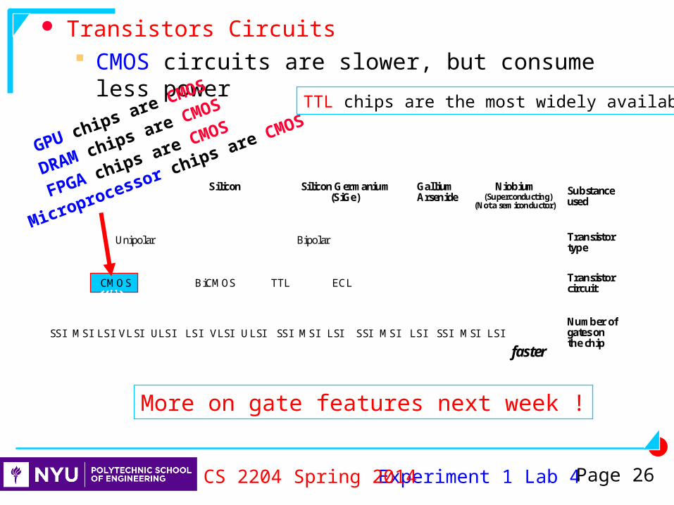
Transistors Circuits CMOS circuits are slower, but consume less
power
Silicon Silicon Germanium GalliumArsenide (Superconducting)
Unipolar
BiCMOSCMOS
Bipolar
SSI MSI LSI VLSI ULSI LSI VLSI ULSI SSI MSI LSI SSI MSI LSI SSI MSI LSI
ECL
Substanceused
Transistortype
Transistorcircuit
Number ofgates onthe chip
(SiGe) Niobium
(Not a semiconductor)
faster
TTL
Experiment 1 Lab 4CS 2204 Spring 2014 Page 26
FPGA chips are CMOS
Microprocessor chips are CMOSTTL chips are the most widely available
More on gate features next week !
DRAM chips are CMOS
GPU chips are CMOS

Silicon Technology Today
Experiment 1 Lab 4CS 2204 Spring 2014 Page 27
a)
b)c)
d)
e)
f) Today : Beyond ULSI Multi- chip module, MCM (>1 die on chip), Giga Scale, etc.
(200M–7B transistors)
Intel Poulson (Itanium) 8 cores
32 Mbyte L3 Cache3.1 Billion transistors,
170 Watts
Will there be an end to shrinking the silicon transistor size ?

Fan-in The maximum number of inputs a gate
can haveThis is purely electricalDetermined by the technology
The electronic circuitry determines how many inputs to have for reliable operation
Experiment 1 Lab 4CS 2204 Spring 2014 Page 28

Fan-out The number of gate inputs that can be connected
to a gate output This is purely electrical Determined by the technology
CMOS gates have the best fan-out If the fan-out is exceeded
The output value may be noisy The output value may not be electrically “strong” to be
interpreted as 1 or 0 The output can be physically damaged
Experiment 1 Lab 4CS 2204 Spring 2014 Page 29

Fan-out In order to increase the fan-out buffers are used
Regular buffers (not input nor output buffers) are used to increase the fan-out
A buffer is an electronic circuit that has no logic function !
It transfers the input to the output with a delay ! It also strengthens the electrical signal
Some buffers are also labeled as drivers since they can electrically “drive” large currents, hence drive many inputs
Some buffers are designed so that they can filter noise on the inputs
Experiment 1 Lab 4CS 2204 Spring 2014 Page 30

Fan-out Increasing the fan-out
Experiment 1 Lab 4CS 2204 Spring 2014 Page 31
a
by
c
..........
Use a buffer !But, the input to output delay is increased

Technology of components/chips Complementary Metal Oxide Semiconductor
(CMOS) Uses unipolar transistors
Slower than Bipolar transistors Consume less power than Bipolar transistors
Not straightforward to connect to TTL chips
Experiment 1 Lab 4CS 2204 Spring 2014 Page 32
Silicon Silicon Germanium GalliumArsenide (Superconducting)
Unipolar
BiCMOSCMOS
Bipolar
SSI MSI LSI VLSI ULSI LSI VLSI ULSI SSI MSI LSI SSI MSI LSI SSI MSI LSI
ECL
Substanceused
Transistortype
Transistorcircuit
Number ofgates onthe chip
(SiGe) Niobium
(Not a semiconductor)
faster
TTL
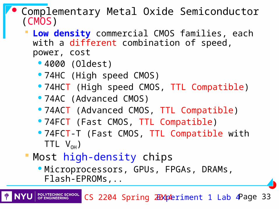
Complementary Metal Oxide Semiconductor (CMOS) Low density commercial CMOS families, each
with a different combination of speed, power, cost4000 (Oldest)74HC (High speed CMOS)74HCT (High speed CMOS, TTL Compatible)74AC (Advanced CMOS)74ACT (Advanced CMOS, TTL Compatible)74FCT (Fast CMOS, TTL Compatible)74FCT-T (Fast CMOS, TTL Compatible with TTL
VOH) Most high-density chips
Microprocessors, GPUs, FPGAs, DRAMs, Flash-EPROMs,..
Experiment 1 Lab 4CS 2204 Spring 2014 Page 33

Complementary Metal Oxide Semiconductor (CMOS)
CMOS chips consume very little power Better Fan-out than TTL chips CMOS chips are sensitive to static
electricity One should not touch them
Unless properly grounded• A wire strapped around the wrist is connected
to the ground • The ground has 0v
Experiment 1 Lab 4CS 2204 Spring 2014 Page 34

Complementary Metal Oxide Semiconductor (CMOS)
Unused gate input 1) Do not leave it unconnected (floating)
Xilinx does not allow this option ! A No Driver warning is given by the Project Manager
Experiment 1 Lab 4CS 2204 Spring 2014 Page 35
a
by
The gate will not work properly
a
b y?
Hi-Z value observed at the input

Digital Engineering Terminology
Experiment 1 Lab 4CS 2204 Spring 2014 Page 36
U1 U2
U3
U4 input has no driverU4 input is not connected to an output. Its input value is Hi-Z (High-Impedance) as there is infinite impedance (resistance) into the U4 input so no current can flow in
a
b
a
c
yU4
Must becorrected

Complementary Metal Oxide Semiconductor (CMOS)
Unused gate input 2) It can be tied to a used input
The fan-out of the b signal may be exceeded !
Experiment 1 Lab 4CS 2204 Spring 2014 Page 37
a
b y An available 3-input AND gate used to implement a 2-input AND gate

Complementary Metal Oxide Semiconductor (CMOS)
Unused gate input 3) It can be connected to 1 or 0 depending on the gate type,
via a pull-up resistor or pull-down resistor
Experiment 1 Lab 4CS 2204 Spring 2014 Page 38
a
b y
+5 v
Pull-upresistor
a
b y
0 v
Pull-downresistor

Complementary Metal Oxide Semiconductor (CMOS) Gate output
Regular
Experiment 1 Lab 4CS 2204 Spring 2014 Page 39
Xilinx warning message fromthe Project Manager :Multiple drivers on output y
Do not short circuit regular gate outputs
y

Digital Engineering Terminology
Experiment 1 Lab 4CS 2204 Spring 2014 Page 40
U1 U2
U3Multiple drivers on output yU3 and U4 outputs are short circuited
a
b
a
c
yU4
Must be corrected

Complementary Metal Oxide Semiconductor (CMOS) Gate output
Tri-state outputs The output has three values !
• 1, 0 and Hi-Z ≡ High-impedance ≡ Floating ≡ Static voltage• There is an extra control input, Enable, to enable/disable output
► If disabled, the output value is Hi-Z (high-impedance)
Experiment 1 Lab 4CS 2204 Spring 2014 Page 41
Enable y
0 Hi-Z
1 ab
Operation table
Tri-state symbol
a
b
y
Enable

Complementary Metal Oxide Semiconductor (CMOS) Gate output
Tri-state outputs A tri-state gate can be envisioned as a regular gate with a switch
at the output
Experiment 1 Lab 4CS 2204 Spring 2014 Page 42
a
b
y
EnableEnable
Regular gate
y
a
b
Switch closed0 1
Switch open
Hi-Z
Output y has three values

Complementary Metal Oxide Semiconductor (CMOS) Gate output :
Tri-state gate outputs can be short circuited if only one gate is enabled at a time
Experiment 1 Lab 4CS 2204 Spring 2014 Page 43
You can short circuit tri-state gate outputs
Enable1
Enable2
Tri-state outputs are often used to implement buses
A bus line
y

Complementary Metal Oxide Semiconductor (CMOS) Gate output :
Open-drain An external pull-up resistor is needed
Experiment 1 Lab 4CS 2204 Spring 2014 Page 44
Open-drain outputs are often used
To drive displays and lights To implement buses
a
b
y
Open drain symbol
+5 v
Pull-upresistor

Complementary Metal Oxide Semiconductor (CMOS) Gate output :
Open-drain Gate outputs can be short circuited
Experiment 1 Lab 4CS 2204 Spring 2014 Page 45
+5 v +5 v
You can short circuit open-drain gate outputs
A bus line

Technology of components/chips Transistor-Transistor Logic (TTL)
Uses bipolar transistors Consists of two sets of families
Commercial : 74xxxx• Cheaper• Widely available
Military : 54xxxx• Manufactured for more stringent applications• Expensive
Experiment 1 Lab 4CS 2204 Spring 2014 Page 46
Silicon Silicon Germanium GalliumArsenide (Superconducting)
Unipolar
BiCMOSCMOS
Bipolar
SSI MSI LSI VLSI ULSI LSI VLSI ULSI SSI MSI LSI SSI MSI LSI SSI MSI LSI
ECL
Substanceused
Transistortype
Transistorcircuit
Number ofgates onthe chip
(SiGe) Niobium
(Not a semiconductor)
faster
TTL

Transistor-Transistor Logic (TTL) Low density commercial TTL families, each
with a different combination of speed, power, cost,..
74 (Standard)74L (Low-power)74S (Schottky)74LS (Low-power Schottky)74H (High speed)74AS (Advanced Schottky)74ALS (Advanced Low-power Schottky)74F (Fast)
Experiment 1 Lab 4CS 2204 Spring 2014 Page 47
We will use itfrom time to time
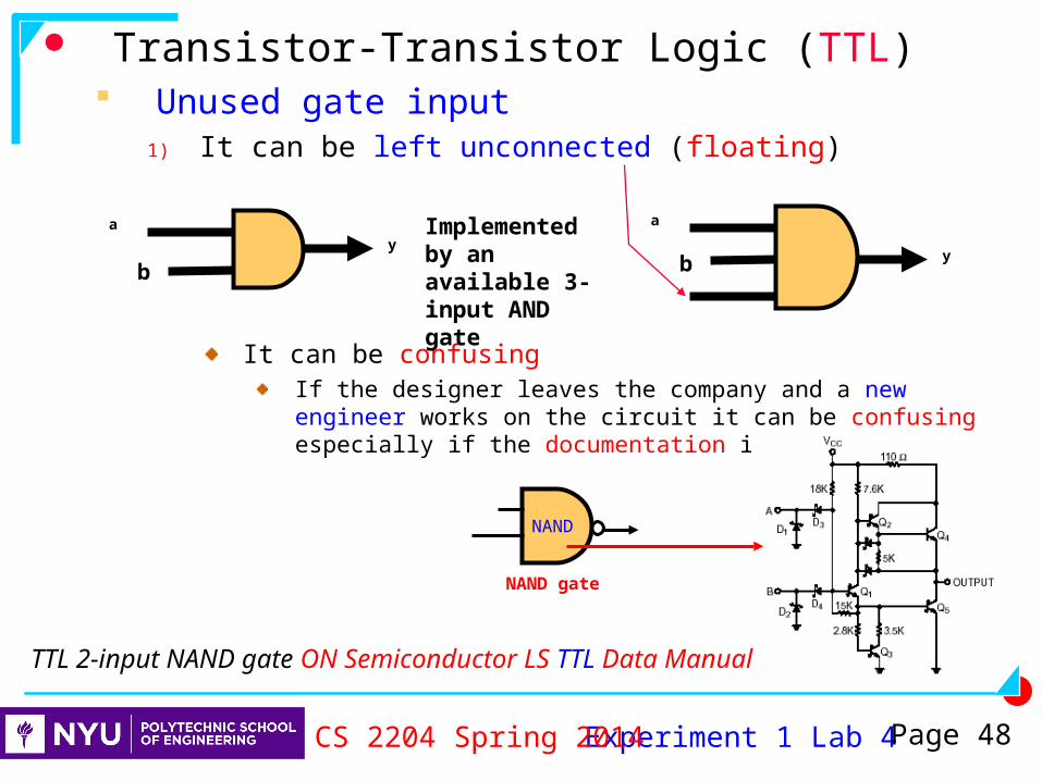
Transistor-Transistor Logic (TTL) Unused gate input
1) It can be left unconnected (floating)
It can be confusingIf the designer leaves the company and a new engineer works on the circuit it can be confusing especially if the documentation is not good !
Experiment 1 Lab 4CS 2204 Spring 2014 Page 48
a
by
Implemented by an available 3-input AND gate
a
b y
TTL 2-input NAND gate ON Semiconductor LS TTL Data Manual
NAND
NAND gate

Transistor-Transistor Logic (TTL) Unused gate input
2) It can be tied to a used input
The fan-out of the b signal can be exceeded
Experiment 1 Lab 4CS 2204 Spring 2014 Page 49
a
b yAn available 3-input AND gate used to implement a 2-input AND gate

Transistor-Transistor Logic (TTL) Unused gate input
3) It can be connected to 1 or 0 depending on the gate type, via a pull-up resistor or pull-down resistor
Experiment 1 Lab 4CS 2204 Spring 2014 Page 50
a
b y
+5 v
Pull-upresistor
a
b y
0 v
Pull-downresistor

Transistor-Transistor Logic (TTL) Gate outputs
Totem-pole outputs
Experiment 1 Lab 4CS 2204 Spring 2014 Page 51
2-input NAND gate implementationFrom ON Semiconductor LS TTL Data Manual

Transistor-Transistor Logic (TTL) Gate outputs
Tri-state outputs The output has three values !
• 1, 0 and Hi-Z ≡ High-impedance ≡ Floating ≡ Static voltage• There is an extra control input, Enable, to enable/disable output
► If disabled, the output value is Hi-Z (high-impedance)
Experiment 1 Lab 4CS 2204 Spring 2014 Page 52
Tri-state symbol
a
b
y
Enable
Enable y
0 Hi-Z
1 ab
Operation table

Transistor-Transistor Logic (TTL) Gate outputs
Tri-state outputs A tri-state gate can be envisioned as a totem-pole gate
with a switch at the output
Experiment 1 Lab 4CS 2204 Spring 2014 Page 53
a
b
y
EnableEnable
Totem-pole gate
y
a
b
Switch closed
0 1
Switch open
Hi-Z
Output y has three values
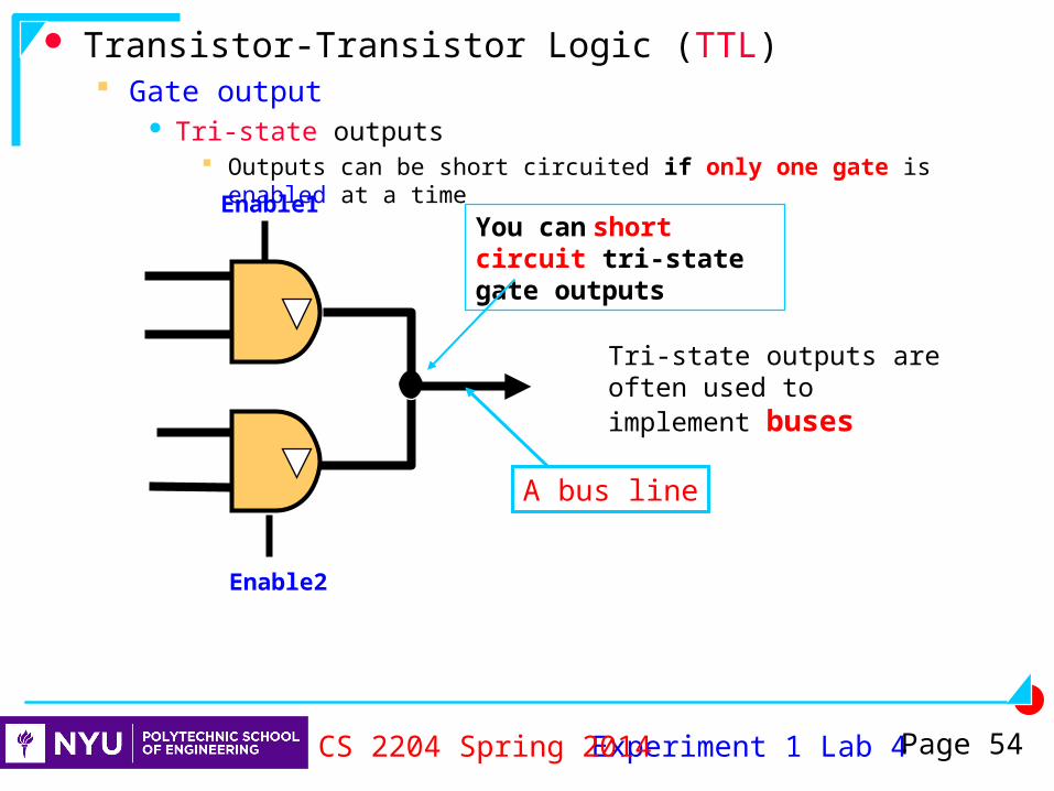
Transistor-Transistor Logic (TTL) Gate output
Tri-state outputs Outputs can be short circuited if only one gate is enabled at a
time
Experiment 1 Lab 4CS 2204 Spring 2014 Page 54
You can short circuit tri-state gate outputs
Enable1
Enable2
Tri-state outputs are often used to implement buses
A bus line
Transistor-Transistor Logic (TTL) Gate output
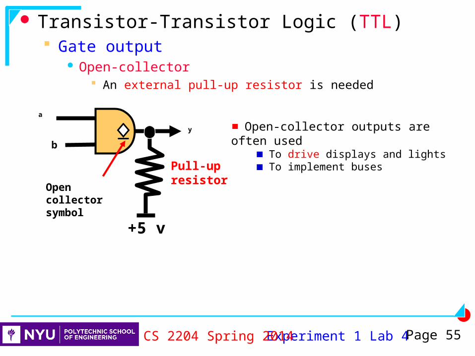
Open-collector An external pull-up resistor is needed
Experiment 1 Lab 4CS 2204 Spring 2014 Page 55
a
b
y
Open collector symbol
+5 v
Pull-upresistor
Open-collector outputs are often used
To drive displays and lights To implement buses

Transistor-Transistor Logic (TTL) Gate output
Open-collector Gate outputs can be short circuited
Experiment 1 Lab 4CS 2204 Spring 2014 Page 56
+5 v +5 v
You can short circuit open-collector gate outputs
Open-collector outputs can be short circuited to implement buses
A bus line

Analysis of the Term Project The term project black-box view The term project operation diagram The term project black box partitioning
Experiment 1 Lab 4CS 2204 Spring 2014 Page 57

The Analysis of the Term Project Polytechnic Playing Machine, Ppm
The term project is human vs. machine
There are two other Ppm versions which are not term projects
Machine vs. machine Human vs. human
Experiment 1 Lab 4CS 2204 Spring 2014 Page 58

The Term Project, Ppm The black-box view
Ppm is sequential (not combinational) A large number of FFs are used ! We need to partition the Ppm based on major operations
• We have to obtain the operation diagram
Experiment 1 Lab 4CS 2204 Spring 2014 Page 59
Figure 1. The Ppm black box view.
Ppm13 19
From the input devices To the output devices

The Term Project, Ppm The black-box view
From page 3 of the Term Project Handout
Experiment 1 Lab 4CS 2204 Spring 2014 Page 60
Clock
Pp
m
P1SEL4
SW7 - SW4
LD2 - LD0
Four 7-Segment Displays
P2playBTN2
P1playBTN3
ResetBTN1
ShptsBTN0
Figure 3. Inputs and outputs of the Ppm term project.
CLK1
LD7 - LD4
P1addSW0
Add
STR0
STR1
STR2
RD0
RD1
RD2
RD3
LD3
A4
A3
A1
A0
CG
CF
CE
CD
CC
CB
CA
TRD3
SW3 - SW1

The term project, Ppm The input/output devices of the Ppm (without clock)
From page 2 of the Term Project Handout
Experiment 1 Lab 4CS 2204 Spring 2014 Page 61
Please be gentle with push buttons and switches
SW7 SW6 SW5 SW4 SW3 SW2 SW1 SW0
LD7 LD6 LD5 LD4 LD3 LD2 LD1 LD0
BTN3 BTN2 BTN1 BTN0
STR
All zero when the
Position Displays
A display blinks fast if display overflow
Reset P1play/ Shpts/
All displays blink if points limit exceeded
P2play
FPGA is downloaded/reset
P1add
Figure 2. FPGA Board Input/Output device utilization of the Ppm Term Project.
PD3 PD2 PD1 PD0
RDAdd
P1SEL
7-segment displays Switches
LED Lights
Push buttons
NextRDs/
Random Digit
Use SW3-SW0 as RD Code digitsCode digits

Ppm Simplified Operation Diagram
Experiment 1 Lab 4CS 2204 Spring 2014 Page 62
Convert the simplified operation diagram to a (detailed) operation diagram
Convert each circle to one or more circles (steps or states)
Reset mode
Player 1 mode
Player 2 mode
Press BTN3 4 times
Press BTN2 to skip
Press BTN2 after playing RD without an
adjacency
Press BTN3 after playing RD with an adjacency
Press BTN2 after playing RD with an adjacency
Press BTN3 after playing RD without an adjacency

Experiment 1 Lab 4CS 2204 Spring 2014 Page 63
PpmInput/outputrelationship
Ppmoperationdiagram
Fro
m p
ag
e 8
of
the T
erm
Pro
ject
Han
dou
t
LD0-LD2 on the FPGA board show the current state
The game is reset : 0 points for players, 0s on position displays !
Player 1 turns on SW0 if wanted. Player 1 turns on and off one of SW7-SW4 to select a position. Player 1 turns off SW0 if on
Player 1 presses BTN2, P2play,
1
2
3
Play
er 1
mod
eP
laye
r 2
mod
e
Download to the FPGA chip
Res
et m
ode
Player 1 points being calculated !
Player 1 presses
BTN 2, P2play, to skip play
Player 1 examines the s ituation !
Player 1 thinks !
4
Player 2 thinks !
5
Player 2 plays on a pos ition
6
Player 1 examines the situation !
Player 2 skips play
(Pla
yer 1
pla
ys)
(Pla
yer
2 p
lays
)
Figure 5. The operation diagram of Ppm.
Player 1 can press BTN3, Reset, in any
Pla
yer
1 c
an p
ress
BT
N4
, Sh
pts
, in
an
y s
tate
to
see
pla
yers
’ p
oin
ts
Player 1 presses BTN3, P1play, four times to play(In
itia
l sta
te)
Player 2 points being calculated !
to allow the machine player to play
Player 1 presses BTN3, P1play,
to allow herself to play again ifthere is an adjacency
Player 1 presses BTN3, P1play, to allow herself to play
Play
er 1
pre
sses
BTN
2, P
2pla
y,
to a
llow
the
mac
hine
pla
yer
to
play
aga
in if
ther
e is
an
adja
cenc
y
0Player 1 can press BTN3, P1play,in state 1 or 3 to see next two RDs
If one of SW7-SW4 is onin state 3, a random digitis input for the machineplayer from SW3-SW0when BTN2 is pressed
state to return to the Reset state, State 0

Experiment 1 Lab 4CS 2204 Spring 2014 Page 64
Points Calculation block
Machine play block
Human play block
Play check block
Machine Play Block is also active states 2 and 5
Input/Output Block
The game is reset : 0 points for players, 0s on position displays !
Player 1 turns on SW0 if wanted. Player 1 turns on and off one of SW7-SW4 to select a position. Player 1 turns off SW0 if on
Player 1 presses BTN2, P2play,
1
2
3Pl
ayer
1 m
ode
Pla
yer
2 m
ode
Download to the FPGA chip
Res
et m
ode
Player 1 points being calculated !
Player 1 presses
BTN 2, P2play, to skip play
Player 1 examines the s ituation !
Player 1 thinks !
4
Player 2 thinks !
5
Player 2 plays on a pos ition
6
Player 1 examines the situation !
Player 2 skips play
(Pla
yer 1
pla
ys)
(Pla
yer
2 p
lays
)
Figure 5. The operation diagram of Ppm.
Player 1 can press BTN3, Reset, in any
Pla
yer
1 c
an p
ress
BT
N4
, Sh
pts,
in
any
sta
te to
see
pla
yers
’ poi
nts
Player 1 presses BTN3, P1play, four times to play(In
itia
l sta
te)
Player 2 points being calculated !
to allow the machine player to play
Player 1 presses BTN3, P1play,
to allow herself to play again ifthere is an adjacency
Player 1 presses BTN3, P1play, to allow herself to play
Play
er 1
pre
sses
BTN
2, P
2pla
y,
to a
llow
the
mac
hine
pla
yer
to
play
aga
in if
ther
e is
an
adja
cenc
y
0Player 1 can press BTN3, P1play,in state 1 or 3 to see next two RDs
If one of SW7-SW4 is onin state 3, a random digitis input for the machineplayer from SW3-SW0when BTN2 is pressed
state to return to the Reset state, State 0
Input/Output Block is active in every state

The Ppm Term Project Partitioning We have observed the following major operations
Interfacing to the input/output devices Handling human player’s play Controlling display operations based on game rules Calculating new player points Determining the machine player play
Hint for general partitioning If you cannot figure out major operations,
partition one major operation at a time
Experiment 1 Lab 4CS 2204 Spring 2014 Page 65

The Ppm Term Project Partitioning Any other major operation ?
Control (time) the operations All other operations
Experiment 1 Lab 4CS 2204 Spring 2014 Page 66
A Digital System
The game is reset : 0 points for players, 0s on position displays !
Player 1 turns on SW0 if wanted. Player 1 turns on and off one of SW7-SW4 to select a position. Player 1 turns off SW0 if on
Player 1 presses BTN2, P2play,
1
2
3
Play
er 1
mod
eP
laye
r 2
mod
e
Download to the FPGA chip R
eset
mod
e
Player 1 points being calculated !
Player 1 presses
BTN 2, P2play, to skip play
Player 1 examines the s ituation !
Player 1 thinks !
4
Player 2 thinks !
5
Player 2 plays on a pos ition
6
Player 1 examines the situation !
Player 2 skips play
(Pla
yer 1
pla
ys)
(Pla
yer
2 p
lays
)
Figure 5. The operation diagram of Ppm.
Player 1 can press BTN3, Reset, in any
Play
er 1
can
pre
ss B
TN
4, S
hpts
, in
any
stat
e to
see
play
ers’
poi
nts
Player 1 presses BTN3, P1play, four times to play(In
itia
l sta
te)
Player 2 points being calculated !
to allow the machine player to play
Player 1 presses BTN3, P1play,
to allow herself to play again ifthere is an adjacency
Player 1 presses BTN3, P1play, to allow herself to play
Play
er 1
pre
sses
BTN
2, P
2pla
y,
to a
llow
the
mac
hine
pla
yer
to
play
aga
in if
ther
e is
an
adja
cenc
y
0Player 1 can press BTN3, P1play,in state 1 or 3 to see next two RDs
If one of SW7-SW4 is onin state 3, a random digitis input for the machineplayer from SW3-SW0when BTN2 is pressed
state to return to the Reset state, State 0
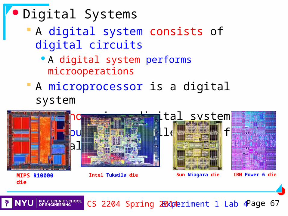
Digital Systems A digital system consists of digital circuits
A digital system performs microoperations
A microprocessor is a digital system An iPhone is a digital system A computer is a collection of digital
systems
Experiment 1 Lab 4CS 2204 Spring 2014 Page 67
Sun Niagara dieIntel Tukwila die IBM Power 6 dieMIPS R10000 die

The Ppm Term Project Ppm is a digital system !
The Ppm term project partitioning First partitioning of the digital system
Control Unit Data Unit
Second partitioning (Data Unit partitioning) Interfacing to the input/output devices Handling human player’s play Controlling display operations based on game rules Calculating new player points Determining the machine player play
Experiment 1 Lab 4CS 2204 Spring 2014 Page 68
core
corecore
corecore
non-core
Figure 1. The Ppm black box view.
Ppm13 19
From the input devices To the output devices

The Ppm Digital System Partitioning
Experiment 1 Lab 4CS 2204 Spring 2014 Page 69
From page 9 of the Term Project Handout

The term project black box partitioning• Six schematics for six blocks
• Block 1 : Control Unit• Block 2 : Input/Output
• Experiment 1 is on a circuit in this block
• Block 3 : Human Play• Block 4 : Play Check• Block 5 : Points Calculation file• Block 6 : Machine
• The Machine Play Block uses all other blocks except the Human Play Block
• These six schematics are in the ppm.sch file
Experiment 1 Lab 4CS 2204 Spring 2014 Page 70

Human Play Block, Block 3 Has 5 inputs and 2 outputs Has only combinational circuits to
Indicates that human player has played P1played
Indicates that the human player has skipped P1skip
Experiment 1 Lab 4CS 2204 Spring 2014 Page 71

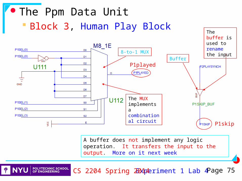
The Ppm Data Unit Block 3, Human Play Block
Very simple for this version of the term project Makes sure the human player does not play on two or
more positions Generates P1played and P1skip signals
It is kept there so that in the future this block can be used to have another machine player so that it becomes machine vs. machine
Experiment 1 Lab 4CS 2204 Spring 2014 Page 72
Block 35 2

The Ppm Data Unit Block 3, Human Play Block
Experiment 1 Lab 4CS 2204 Spring 2014 Page 73
Block 35 2
From page 21 of the Term Project Handout
P1SEL4
P1skip
P1played
Figure 12. The detailed view of the input and output signals of the Human Play Block.
Human Play Block
P2playsynchCore
Block 3
Player 1 has skipped
Player 1 has played

The Ppm Data Unit Block 3, Human Play Block
Experiment 1 Lab 4CS 2204 Spring 2014 Page 74
The circuit that generates the P1played signal
The circuit that generates the P1skip signal
P1played is 1 if only one position is played by the human player
The MUX circuit implements a combinational circuit as will be
discussed in class The circuit ensures only one position is played
The Ppm Data Unit Block 3, Human Play Block
Experiment 1 Lab 4CS 2204 Spring 2014 Page 75
8-to-1 MUXBuffer
The buffer is used to rename the input
A buffer does not implement any logic operation. It transfers the input to the output. More on it next week
P1played
P1skip
The MUX implements a combinational circuit

Assignment by next lab Make sure that you have completed Experiment 1
Your experiment will be collected and graded The last day to submit Experiment 1 as a team is Friday,
March 7, 2014• We will also collect Experiment 2, by Friday, March 7, 2014
It will be graded and returned by the following lab
Experiment 1 Lab 4CS 2204 Spring 2014 Page 76
Submit your Experiment 1 during a lab session !
Not during Open Lab Hours !

Digital Design Conventions Digital Circuit Drawing Conventions
Project Information is placed in the lower right corner
Company name, and address Project name, Project dates, etc.
Experiment 1 Lab 4CS 2204 Spring 2014 Page 77

Digital Design Conventions Digital Circuit Drawing Conventions
CS2204 Related Part 1 of Term Project Design Checks
• The team info on the lower right corner is ► In the Name area enter the name of the student who designed
the schematic + the names of the other members of the team
► In the Title area enter “ CS 2204 – Your Lab Section – Spring 2014” Place some space before “CS 2204” so that it is
not right next to the name of the block
Experiment 1 Lab 4CS 2204 Spring 2014 Page 78

Digital Design Conventions Digital Circuit Drawing Conventions
Part 2 of Term Project Design Checks Remember to beautify the circuit before submitting
it• Place components of a (sub)block next to each
other and separate (sub)blocks from each other• Components form horizontal and vertical lines• Only horizontal and vertical wires drawn• No need to draw long wires
► One can draw short wires and name them
• No unnecessary wire turns• No Unnecessary line tanglings• Wires are not drawn over components, buffers,
pads
Experiment 1 Lab 4CS 2204 Spring 2014 Page 79

Digital Design Conventions Logic Circuit Design Conventions
Part 3 of Term Project Design Checks If a component has multiple outputs, make sure you
use the needed ones• If an output is not needed, leave it unconnected
Outputs should not be short-circuited unless they are tri-state
• But, we will not use tri-state outputs this semester !
Experiment 1 Lab 4CS 2204 Spring 2014 Page 80

Digital Design Conventions Logic Circuit Design Conventions
Part 4 of Term Project Design Checks Make sure the experiment folder name is correct Last experiment folder is used for the current
experiment ?• The termproject folder is used as the experiment
folder ? More than 6 schematics are used ?
Experiment 1 Lab 4CS 2204 Spring 2014 Page 81

Digital Design Conventions Logic Circuit Design Conventions
Part 5 of Term Project Design Checks Do not forget to save schematics
• Then, do a Xilinx IMPLEMENTATION to have the changes affect the output
Read the warnings and errors listed• Confirm that the warnings are acceptable• The FPGA chip utilization does not have to be 6% ► The utilization depends on the strategy, the intelligence
of the machine player designed
Perform simulations• If an output value is Hi-Z during simulation, make
sure it is correct
Experiment 1 Lab 4CS 2204 Spring 2014 Page 82

Digital Design Conventions Digital Circuit Printing Conventions
The printout must be readable Labels, component names, symbols, etc.
If the circuit is large, it must be printed on several pages
The sheets must be attached to each other Lines, labels, etc. must be continuous from one
sheet to the next
Experiment 1 Lab 4CS 2204 Spring 2014 Page 83

Common Logic Errors Discovering logic errors by means of simulations
Experiment 1 Lab 4CS 2204 Spring 2014 Page 84
U3
The OR gate is an AND gate by mistake !
Input “a” is input “b” by mistake !
Must becorrected
Must be corrected
b
a
c
b
y(a, b, c) =y(a, b, c) = a.b + a.ca.b + a.c
The correct expression
y(a, b, c) =y(a, b, c) = a.ba.b.(b.(b.c.c))
The incorrectexpression

Common Logic Errors Discovering logic errors by means of simulations
Experiment 1 Lab 4CS 2204 Spring 2014 Page 85
U1 U2
U3
U2 has no LoadU2 output is not used
Multiple drivers on output yU3 and U4 outputs are short circuited
U4 input has no driverU4 input is not connected to an output. Its input value is Hi-Z (High-Impedance) as there is infinite impedance (resistance) into the U4 input so no current can flow in
a
b
a
c
yU4
Must becorrected
Must becorrected
Must be corrected

QUESTIONS ?
Experiment 1 Lab 4CS 2204 Spring 2014 Page 86
DigitalLogic and
State Machine Design
Read slides at the end to learn about the software, Project Manager, Schematic design and other related topics
Continue reading the Term Project handout
Think about the machine player strategy
Do not leave the lab before your partners finish► Help your partners
Make sure you have the LABS account and see the S driveMake sure you have installed WebPACK 12.4 on your laptop
Make sure you create a CS2204 folder on both

Today’s Individual Xilinx Work We will continue with the 4-bit 2-to-1 MUX in Block 2. We
will use our knowledge of 2-to-1 MUXes to modify a portion of the term project to develop a 4-bit 2-to-1 MUX in the Human Play Block (Block 3)
The 2-to-1 MUX expression is the same as the one obtained in class
We will obtain its schematic (circuit diagram)• We will design a 4-bit MUX by using 1-bit MUXes
We will do a schematic check We will test our design on the computer assuming ideal gates
• Do logic simulations We will do a Xilinx IMPLEMENTATION of the project
• To create the bit file We will test our design on the FPGA board
• We will program the FPGA chip ≡ download the bit file• We will use switches and a LED light to test our design on the FPGA
board Help our partners complete today’s project We will continue reading the Term Project handout
Also read slides at the end to learn about the software, Project Manager, Schematic design and other related topics
Experiment 1 Lab 4CS 2204 Spring 2014 Page 87

Today’s Individual Xilinx Lab Work1. (If you did not do it last week) Copy the termproject
folder and paste it as the exp1 folder to experiment with the Ppm schematics
2. Start the Xilinx ISE software and open the Ppm project in the exp1 folder
3. Open the schematics and analyze the schematicsMake sure the team info is placed on all the schematics !
4. Study the 4-bit 2-to-1 MUX schematic in the Input/Output Block in schematic 2 of the term project to refresh your memory on the MUX
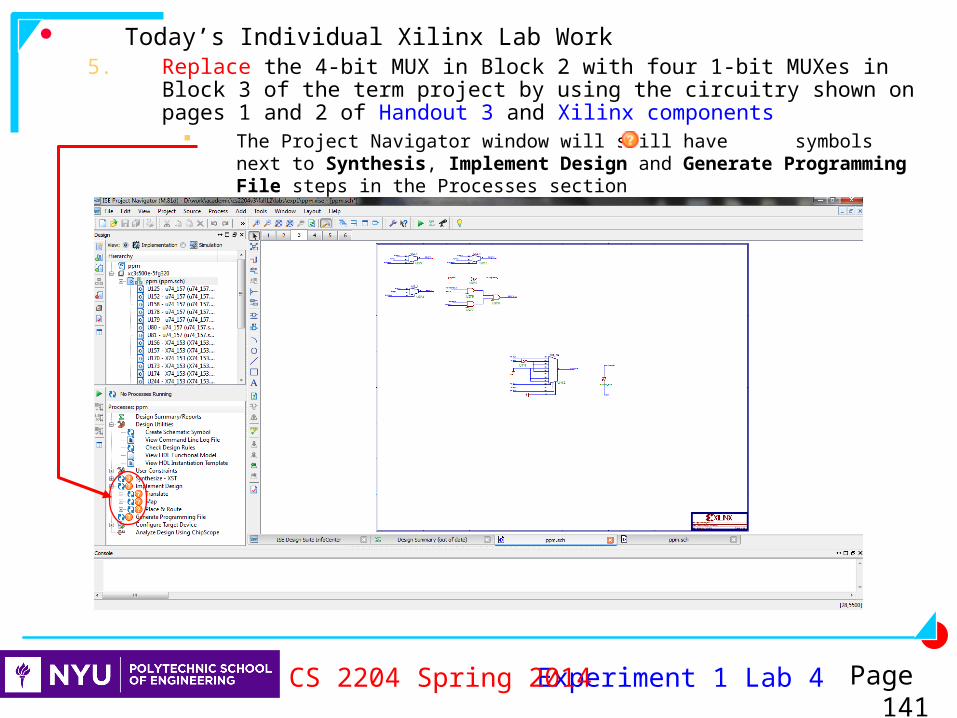
5. Replace the 4-bit MUX in Block 2 with four 1-bit MUXes in Block 3 of the term project by using the circuitry shown on pages 1 and 2 of Handout 3 and Xilinx components
6. Do a schematic check on the new design7. Perform functional simulations on the 4-bit 2-to-1 MUX
Experiment 1 Lab 4CS 2204 Spring 2014 Page 88

Today’s Individual Xilinx Lab Work8. Perform a Xilinx IMPLEMENTATION9. Download the Ppm project to the FPGA chip and play the
game and to verify that the schematic works correctly Program the FPGA chip
Test the Ppm to see if it is working• Play the game on the FPGA board
If it does not work, inspect your circuit in Block 3 and correct the circuit
10. Help your partners complete today’s project11. Submit your exp1 project once everyone completes the
design12. Continue reading the Term Project handout
Study and play the other two types of the Ppm game to think more about the our machine player’s strategy Human vs. human : ppmhvsh Machine vs. machine : ppmmvsm
• Think about the playing strategy of the machine player that will be designed
Also read slides at the end to learn about the software, Project Manager, Schematic design and other related topics
Experiment 1 Lab 4CS 2204 Spring 2014 Page 89

Today’s Individual Xilinx Lab Work1. (If you did not do this step last week) Copy the
termproject folder in the CS2204 folder on the S drive and paste it as the exp1 folder to experiment with the Ppm schematics as explained in the Lab 3 presentation
2. Start the Xilinx ISE software and open the Ppm project in the exp1 folder
Double click on the Xilinx ISE Design Suite icon on your desktop :
Experiment 1 Lab 4CS 2204 Spring 2014 Page 90

Today’s Individual Xilinx Work2. Start the Xilinx ISE software and open the Ppm project in
the exp1 folder Xilinx will show a “Tip of the Day” window in the foreground
and the “ISE Project Navigator” window in the background :
Experiment 1 Lab 4CS 2204 Spring 2014 Page 91

Today’s Individual Xilinx Work2. Start the Xilinx ISE software and open the Ppm project in the
exp1 folder The ISE opens the last project you worked on by default
Though this can be changed by changing the Preferences settings If you did not open any Xilinx project, it will not open any project as you
saw on the previous slide and see below Click on OK to close the “Tip of the Day” window :
Experiment 1 Lab 4CS 2204 Spring 2014 Page 92
Note that this window can be turned off by clicking on this :

Today’s Individual Xilinx Work2. Start the Xilinx ISE software and open the Ppm project in
the exp1 folder After the “Tip of the Day” window is closed you will see the
following :
Experiment 1 Lab 4CS 2204 Spring 2014 Page 93

Today’s Individual Xilinx Work2. Start the Xilinx ISE software and open the Ppm project in
the exp1 folder Click on Open Project... on the “Start” panel on the left to
start opening the term project
Experiment 1 Lab 4CS 2204 Spring 2014 Page 94

Today’s Individual Xilinx Work2. Start the Xilinx ISE software and open the Ppm project in the
exp1 folder The “Open Project”window will pop up asking you to select the project
folder which is termproject Select the project folder S;\CS2204\exp1 by using typical Windows
operations You will see the partial content of the exp1 folder where all six folders and
the “Xilinx ISE Project” file are shown :
Experiment 1 Lab 4CS 2204 Spring 2014 Page 95

Today’s Individual Xilinx Work2. Start the Xilinx ISE software and open the Ppm project in the
exp1 folder Double click on “Xilinx ISE Project” :
Experiment 1 Lab 4CS 2204 Spring 2014 Page 96
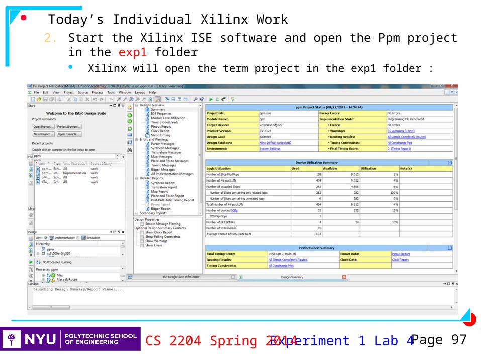
Today’s Individual Xilinx Work2. Start the Xilinx ISE software and open the Ppm project in the
exp1 folder Xilinx will open the term project in the exp1 folder :
Experiment 1 Lab 4CS 2204 Spring 2014 Page 97

Today’s Individual Xilinx Work3. Open the schematics and analyze the schematics
Double click on ppm (ppm.sc) to view the six schematics
Experiment 1 Lab 4CS 2204 Spring 2014 Page 98

Today’s Individual Xilinx Work3. Open the schematics and analyze the
schematics Take a look at the six schematics for the six
blocks of the term project• Block 1 : Control Unit• Block 2 : Input/Output• Block 3 : Human Play• Block 4 : Play Check• Block 5 : Points Calculation• Block 6 : Machine Play
These six schematics are in the ppm.sch file
Experiment 1 Lab 4CS 2204 Spring 2014 Page 99

Today’s Individual Xilinx Work3. Open the schematics and analyze the schematics
Double click on ppm (ppm.sc) to view the six schematics Notice that as the schematic file is open the first schematic sheet is shown
and also the left panel changes to the “Options” panel :
Experiment 1 Lab 4CS 2204 Spring 2014 Page 100
First schematic sheet : Control Unit
First schematic sheet

Today’s Individual Xilinx Work3. Open the schematics and analyze the schematics
Click on 2 to the left of the schematic sheet to view the second schematic sheet :
Experiment 1 Lab 4CS 2204 Spring 2014 Page 101
Second schematic sheet : Input/Output Block
Secondschematic sheet

Today’s Individual Xilinx Work3. Open the schematics and analyze the schematics
Click on 3 to the left of the schematic sheet to view the third schematic sheet :
Experiment 1 Lab 4CS 2204 Spring 2014 Page 102
Thirdschematic sheet Third
schematic sheet : Human Play Block

Today’s Individual Xilinx Work3. Open the schematics and analyze the schematics
Click on 4 to the left of the schematic sheet to view the fourth schematic sheet :
Experiment 1 Lab 4CS 2204 Spring 2014 Page 103
Fourthschematic sheet Fourth
schematic sheet : Play Check Block

Today’s Individual Xilinx Work3. Open the schematics and analyze the schematics
Click on 5 to the left of the schematic sheet to view the fifth schematic sheet :
Experiment 1 Lab 4CS 2204 Spring 2014 Page 104
Fifthschematic sheet Fifth
schematic sheet : Points CalculationBlock
Today’s Individual Xilinx Work3. Open the schematics and analyze the schematics
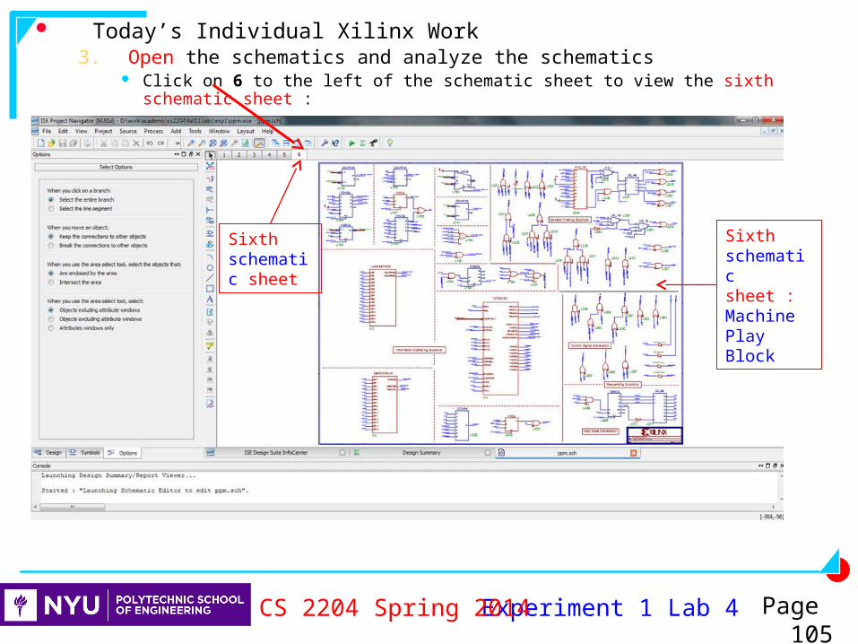
Click on 6 to the left of the schematic sheet to view the sixth schematic sheet :
Experiment 1 Lab 4CS 2204 Spring 2014 Page 105
Sixthschematic sheet
Sixthschematic sheet : Machine PlayBlock

Today’s Individual Xilinx Work3. Open the schematics and analyze the
schematics There are six schematics !
Experiment 1 Lab 4CS 2204 Spring 2014 Page 106
The Term Project handout discusses the schematics in detail !
We are covering these schematics in detail !

Today’s Individual Xilinx Work3. Open the schematics and analyze the
schematics Take a look at the six schematics for the six blocks of
the term project• Blocks 1, 2, 3, 4 and 5 are core blocks
• All of their circuits are given
• Block 6 is completely non-core• Students will replace all the circuits with their own circuits
Experiment 1 Lab 4CS 2204 Spring 2014 Page 107

Today’s Individual Xilinx Lab Work3. Open the schematics and analyze the
schematics Take a look at the six schematics for the six
blocks of the term project• Each block (schematic) consists of subblocks and
subsubblocks• The software identifies each schematic sheet by
automatically assigning it a number• Subblocks and subsubblocks are identified by
their names and distance and lines between them on the schematic sheet
• Common document processor editing rules and key sequences apply to edit schematics
Experiment 1 Lab 4CS 2204 Spring 2014 Page 108
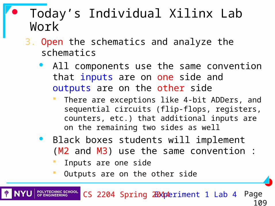
Today’s Individual Xilinx Lab Work3. Open the schematics and analyze the
schematics All components use the same convention
that inputs are on one side and outputs are on the other side There are exceptions like 4-bit ADDers, and
sequential circuits (flip-flops, registers, counters, etc.) that additional inputs are on the remaining two sides as well
Black boxes students will implement (M2 and M3) use the same convention : Inputs are one side Outputs are on the other side
Experiment 1 Lab 4CS 2204 Spring 2014 Page 109

Today’s Individual Xilinx Lab Work3. Open the schematics and analyze the schematics
Enter team information on the schematics if it is not entered• To enter the team info schematic 1 switch to schematic 1 and
zoom into the lower right corner where project information is shown :
Experiment 1 Lab 4CS 2204 Spring 2014 Page 110

Today’s Individual Xilinx Lab Work3. Open the schematics and analyze the schematics
Enter team information on the schematics if it is not entered• To enter the team info on schematic 1 switch to schematic 1 and
zoom into the lower right corner where project information is shown :
• Right click on the project information object• Select Object Properties• In the NameFieldText area enter the names of the members of the
team• In the Title area enter “ CS 2204 – Your Lab Section – Spring
2014” • Place some space before “CS 2204” so that it is not right next
to “Ppm Control Unit”
Experiment 1 Lab 4CS 2204 Spring 2014 Page 111
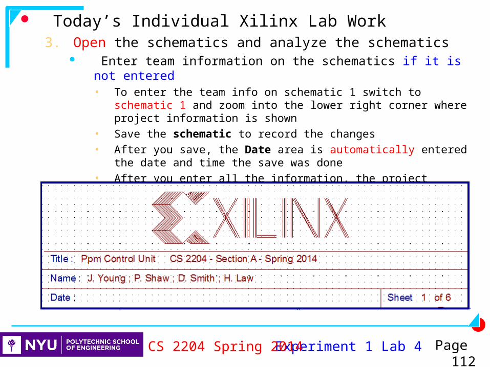
Today’s Individual Xilinx Lab Work3. Open the schematics and analyze the schematics
Enter team information on the schematics if it is not entered• To enter the team info on schematic 1 switch to schematic 1 and
zoom into the lower right corner where project information is shown
• Save the schematic to record the changes• After you save, the Date area is automatically entered the date
and time the save was done• After you enter all the information, the project information area
in schematic 1 will look like as follows for an imaginary team :
Experiment 1 Lab 4CS 2204 Spring 2014 Page 112

Today’s Individual Xilinx Lab Work3. Open the schematics and analyze the schematics
Enter team information on the schematics if it is not entered The Project Navigator window after the schematic is saved is different
where there are symbols next to Synthesis, Implement Design and Generate Programming File steps in the Processes section, signaling that they must be done to incorporate these changes to the design
Experiment 1 Lab 4CS 2204 Spring 2014 Page 113

Today’s Individual Xilinx Lab Work3. Open the schematics and analyze the schematics
Enter team information on the schematics if it is not entered Repeat these steps above for the remaining five schematics so that they
all have the same team information The Project Navigator window will still have symbols next to
Synthesis, Implement Design and Generate Programming File steps in the Processes section
Experiment 1 Lab 4CS 2204 Spring 2014 Page 114

Today’s Individual Xilinx Lab Work3. Open the schematics and analyze the schematics
Enter team information on the schematics if it is not entered Repeat these steps above for the remaining five schematics so that they
all have the same team information The Project Navigator window will still have symbols next to
Synthesis, Implement Design and Generate Programming File steps in the Processes section
In order to record these changes, we have to save the schematic and do a synthesis• Save the schematic• Perform a Synthesis operation by double clicking on the
Synthesize – XST process on the Project Navigator panel• Switch to the Design Summary panel and notice that there
are 137 warnings We know this due to the fact that we are working on a copied
and pasted project and the ISE is complaining about the paths• Right click and select ReRun on the Synthesize – XST
process on the Project Navigator panel to eliminate the unnecessary warnings
The new number of warnings is 63 as it is the case with the term project and the symbol next to the Synthesize – XST process is
Experiment 1 Lab 4CS 2204 Spring 2014 Page 115

Today’s Individual Xilinx Lab Work4. Study the 4-bit 2-to-1 MUX schematic in the Input/Output
Block in schematic 2 of the term project to refresh your memory on the MUXa) Take a look at the MUX labeled U80
DDISP circuit is a 4-bit 2-to-1 MUX• Selects between DISP and P2PT• Uses DISPSEL0 as the select signal
Experiment 1 Lab 4CS 2204 Spring 2014 Page 116
We need a 4-bit 2-to-1 MUX
Do we design it ?
DDISP operation tableDISPSEL0 Operation
0 DDSIP = DISP
1 DDISP = P2PT

Today’s Individual Xilinx Lab Work4. Study the 4-bit 2-to-1 MUX schematic in the Input/Output
Block in schematic 2 (ppm2.sch) of the term project to refresh your memory on the MUX
a) Take a look at the MUX labeled U80 DDISP circuit is a 4-bit 2-to-1 MUX
Experiment 1 Lab 4CS 2204 Spring 2014 Page 117
u74_157A
4-bit 2-to-1 MUX
We need a 4-bit 2-to-1 MUX
We do not design it : Ithas already implemented &it is satisfactory for us

Today’s Individual Xilinx Lab Work4. Study the 4-bit 2-to-1 MUX schematic in the Input/Output Block in
schematic 2 of the term project to refresh your memory on the MUXa) Take a look at the MUX labeled U80
What is the G input ?• The G input is a control input which is the enable input• If the Enable input is 1 all four outputs are 0• The G input is active low !
• The circle (bubble) at the G input indicates it is active low ! simulations on the 4-bit 2-to-1 MUX in to refresh your memory on the MUX and simulations
Experiment 1 Lab 4CS 2204 Spring 2014 Page 118
The 4-bit 2-to-1MUX operation table
S Operation
0 0 Y = A
0 1 Y = B
G
1 X Y = 0

Today’s Individual Xilinx Lab Work4. Study the 4-bit 2-to-1 MUX schematic in the Input/Output Block
in schematic 2 of the term project to refresh your memory on the MUXa) Take a look at the MUX labeled U80
What is the GND ?• GND ≡ Ground ≡ 0 Volts ≡ 0• The G input is permanently connected to 0 !• Since the Enable is permanently 0, the outputs are always enabled
Experiment 1 Lab 4CS 2204 Spring 2014 Page 119
How DDISP uses the MUX
DISPSEL0 Operation
0 0 DDISP = DISP
0 1 DDISP = P2PT
G
1 X DDISP = 0
G = 0 Only these two rows are valid for U80

Today’s Individual Xilinx Lab Work4. Study the 4-bit 2-to-1 MUX schematic in the Input/Output
Block in schematic 2 of the term project to refresh your memory on the MUXa) Take a look at the MUX labeled U80
Implementing a 4-bit 2-to-1 MUX ?• Based on major operations on the operation table !• Major operations are not explicit on the previous operation
table• Obtain a more detailed operation table
• There are four identical major operations : 1-bit 2-to-1 MUXing
Experiment 1 Lab 4CS 2204 Spring 2014 Page 120
The 4-bit 2-to-1 MUX operation table
S Operation
0 0 Y = A0 1 Y = B
G
1 X Y = 0
The 4-bit 2-to-1 MUX operation table
S Operation
0 0 Y3=A3, Y2=A2, Y1=A1, Y0=A00 1 Y3=B3, Y2=B2, Y1=B1, Y0=B0
G
1 X Y3=0, Y2=0, Y1=0, Y0=0

Today’s Individual Xilinx Lab Work4. Study the 4-bit 2-to-1 MUX schematic in the Input/Output
Block in schematic 2 of the term project to refresh your memory on the MUX
a) Take a look at the MUX labeled U80 See how the 4-bit 2-to-1 MUX is designed
• Do a Hierarchy Push to see the implementation of the 4-bit 2-to-1 MUX by
• Right clicking on the MUX and selecting Symbol -> Push into Symbol
• Confirm that it has four 1-bit Xilinx 2-to-1 MUXes
• See the implementation of the 4-bit MUX on the next slide
Experiment 1 Lab 4CS 2204 Spring 2014 Page 121

Today’s Individual Xilinx Lab Work4. Study the 4-bit 2-to-1 MUX schematic in the Input/Output Block
in schematic 2 of the term project to refresh your memory on the MUX
a) Take a look at the MUX labeled U80
Experiment 1 Lab 4CS 2204 Spring 2014 Page 122
The 4-bit 2-to-1 MUX operation table
S Operation
0 0 Y3=A3, Y2=A2, Y1=A1, Y0=A0
0 1 Y3=B3, Y2=B2, Y1=B1, Y0=B0
G
1 X Y3=0, Y2=0, Y1=0, Y0=0

Today’s Individual Xilinx Lab Work4. Study the 4-bit 2-to-1 MUX schematic in the Input/Output
Block in schematic 2 of the term project to refresh your memory on the MUX
a) Take a look at the MUX labeled U80 Do another Hierarchy Push to see the
implementation of one of the (1-bit) 2-to-1 MUXes and confirm that it is similar what we discussed in class, except• The AND gates have three inputs since the
enable input is connected to the AND gates to control the output
• The separate inverter we have in mux2to1 is implemented by a special Xilinx AND gate, AND3B1
► One input of the AND gate is internally inverted
• See the Xilinx implementation of the 1-bit MUX on the next slide
Experiment 1 Lab 4CS 2204 Spring 2014 Page 123

Today’s Individual Xilinx Lab Work4. Study the 4-bit 2-to-1 MUX schematic in the Input/Output
Block in schematic 2 (ppm2.sch) of the term project to refresh your memory on the MUXa) Take a look at the MUX labeled U80
Experiment 1 Lab 4CS 2204 Spring 2014 Page 124
A Xilinx specific 3-input AND gate with an input inverted internally : AND3B1
Xilinx 1-bit 2-to-1 MUX operation table
S Operation
0 0 O = D0
0 1 O = D1
E
1 X O = 0

Today’s Individual Xilinx Lab Work4. Study the 4-bit 2-to-1 MUX schematic in
the Input/Output Block in schematic 2 of the term project to refresh your memory on the MUXa) Take a look at the MUX labeled U80
Close the two schematics by clicking on the Close Tab buttons on the bottom of the schematic display
Experiment 1 Lab 4CS 2204 Spring 2014 Page 125

Today’s Individual Xilinx Lab Work4. Study the 4-bit 2-to-1 MUX schematic in the Input/Output Block
in schematic 2 of the term project to refresh your memory on the MUX
b) Perform functional simulations on the 4-bit 2-to-1 MUX in to refresh your memory on the MUX and simulations :
Experiment 1 Lab 4CS 2204 Spring 2014 Page 126

Today’s Individual Xilinx Lab Work5. Replace the 4-bit MUX in Block 2 with four 1-bit MUXes
in Block 3 of the term project by using the circuitry shown on pages 1 and 2 of Handout 3 and Xilinx components
a) Delete the 4-bit 2-to-1 MUX in Schematic 2 Switch to schematic 2, if it is not the schematic viewed
Experiment 1 Lab 4CS 2204 Spring 2014 Page 127

Today’s Individual Xilinx Lab Work5. Replace the 4-bit MUX in Block 2 with four 1-
bit MUXes in Block 3 of the term project by using the circuitry shown on pages 1 and 2 of Handout 3 and Xilinx components
a) Delete the 4-bit 2-to-1 MUX in Schematic 2 Select the 4-bit 2-to-1 MUX by clicking on it Press Delete to delete it
• Do not delete the wires of the MUX See modified schematic 2 on the next slide
Experiment 1 Lab 4CS 2204 Spring 2014 Page 128

Today’s Individual Xilinx Lab Work5. Replace the 4-bit MUX in Block 2 with four 1-bit MUXes
in Block 3 of the term project by using the circuitry shown on pages 1 and 2 of Handout 3 and Xilinx components
Experiment 1 Lab 4CS 2204 Spring 2014 Page 129
4-bit2-to-1 MUXdeleted

Today’s Individual Xilinx Lab Work5. Replace the 4-bit MUX in Block 2 with four 1-bit MUXes
in Block 3 of the term project by using the circuitry shown on pages 1 and 2 of Handout 3 and Xilinx components
b) Switch to the Human Play Block, Block 3c) Zoom into the upper left side of the schematicd) Place a Xilinx 1-bit 2-to-1 MUX, M2_1, in the very upper left
corner of the schematic as shown on page 1 of Handout 3 and on the next two slides The wire names are changed
• Input A is DISPSEL0 (The Xilinx name is S0)• Input B is DISP12 (The Xilinx name is D0)• Input C is P2PT(4) (The Xilinx name is D1)• Output Y is DDISP12 (The Xilinx name is O)
Give label U272 (because the last component label is U271 in Block 6) to the MUX
See next two slides to visualize this MUX
Experiment 1 Lab 4CS 2204 Spring 2014 Page 130

Today’s Individual Xilinx Lab Work5. Replace the 4-bit MUX in Block 2 with four 1-bit MUXes
in Block 3 of the term project by using the circuitry shown on pages 1 and 2 of Handout 3 and Xilinx components
Experiment 1 Lab 4CS 2204 Spring 2014 Page 131
1-bit 2-to-1 MUX

Today’s Individual Xilinx Lab Work5. Replace the 4-bit MUX in Block 2 with four 1-bit MUXes
in Block 3 of the term project by using the circuitry shown on pages 1 and 2 of Handout 3 and Xilinx components
Experiment 1 Lab 4CS 2204 Spring 2014 Page 132
1-bit 2-to-1 MUX

Today’s Individual Xilinx Lab Work5. Replace the 4-bit MUX in Block 2 with four 1-bit MUXes in
Block 3 of the term project by using the circuitry shown on pages 1 and 2 of Handout 3 and Xilinx components
e) Place two more Xilinx 1-bit 2-to-1 MUXes, M2_1, in the upper left corner of the schematic as shown on page 1 of Handout 3 and on the next two slides Copy the circuit just selected Right click anywhere on the screen select Paste
Special… When the “Paste Special” window is shown select Use
new name for all nets and then click OK Place the copied Xilinx MUX to the right side of the (1-bit) 2-to-1
MUX just designed• Rename the inputs and outputs as DISP13, P2PT(5), DISPSEL0
and DDISP13, respectively Repeat the above steps to place one more Xilinx MUX to place it
below the first (1-bit) 2-to-1 MUX designed• Rename the inputs and outputs as DISP14, P2PT(6), DISPSEL0
and DDISP14, respectively Give labels U273 and U274 to the MUXes just placed See next two slides to visualize these MUXes
Experiment 1 Lab 4CS 2204 Spring 2014 Page 133

Today’s Individual Xilinx Lab Work5. Replace the 4-bit MUX in Block 2 with four 1-bit MUXes
in Block 3 of the term project by using the circuitry shown on pages 1 and 2 of Handout 3 and Xilinx components
e) Place two more Xilinx 1-bit 2-to-1 MUXes
Experiment 1 Lab 4CS 2204 Spring 2014 Page 134
Three1-bit2-to-1MUXes

Today’s Individual Xilinx Lab Work5. Replace the 4-bit MUX in Block 2 with four 1-bit MUXes
in Block 3 of the term project by using the circuitry shown on pages 1 and 2 of Handout 3 and Xilinx components
Experiment 1 Lab 4CS 2204 Spring 2014 Page 135
The new 1-bit 2-to-1 MUXes

Today’s Individual Xilinx Lab Work5. Replace the 4-bit MUX in Block 2 with four 1-bit MUXes
in Block 3 of the term project by using the circuitry shown on pages 1 and 2 of Handout 3 and Xilinx components
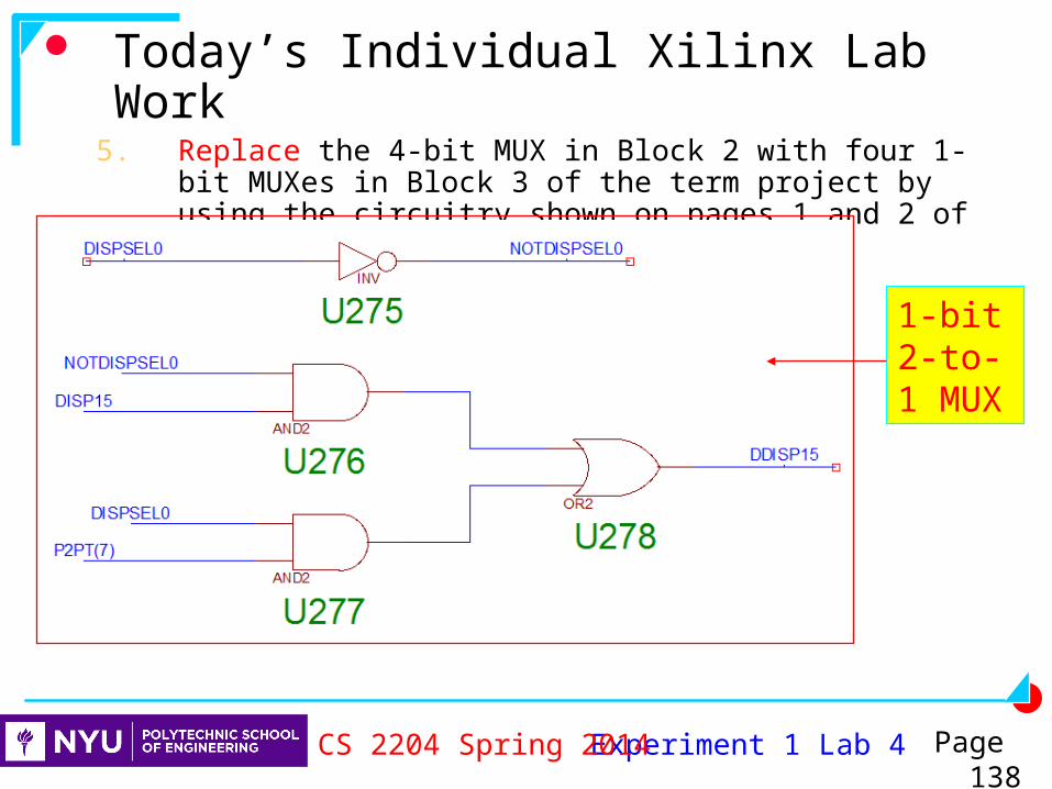
f) Place the last MUX as a gate network Draw the gate network, a 1-bit 2-to-1 MUX as explained
in the classroom with the following exceptions The wire names are changed
• Input A is DISPSEL0• Input B is DISP15• Input C is P2PT(7)• Output Y is DDISP15• The output of the NOT gate is labeled NotDISPSEL0
Label the gates starting at U275• The NOT gate is labeled U275 • The AND gates are labeled U276 and U277• The OR gate is labeled U278
See next two slides to visualize this MUX
Experiment 1 Lab 4CS 2204 Spring 2014 Page 136

Today’s Individual Xilinx Lab Work5. Replace the 4-bit MUX in Block 2 with four 1-bit MUXes
in Block 3 of the term project by using the circuitry shown on pages 1 and 2 of Handout 3 and Xilinx components
f) Place the last MUX as a gate network
Experiment 1 Lab 4CS 2204 Spring 2014 Page 137
4-bit2-to-1MUX
Today’s Individual Xilinx Lab Work5. Replace the 4-bit MUX in Block 2 with four 1-bit MUXes
in Block 3 of the term project by using the circuitry shown on pages 1 and 2 of Handout 3 and Xilinx components
Experiment 1 Lab 4CS 2204 Spring 2014 Page 138
1-bit 2-to-1 MUX

Today’s Individual Xilinx Lab Work5. Replace the 4-bit MUX in Block 2 with four 1-bit MUXes
in Block 3 of the term project by using the circuitry shown on pages 1 and 2 of Handout 3 and Xilinx components
f) Place the last MUX as a gate network Make sure that you
• Appropriately name the new wires• Appropriately label the new gates The last component label is U278
Make sure your circuit is beautified so that it is easier to follow the schematic
Save the schematic See modified Block 3 on the next slide
Experiment 1 Lab 4CS 2204 Spring 2014 Page 139

Today’s Individual Xilinx Lab Work5. Replace the 4-bit MUX in Block 2 with four 1-bit MUXes in Block 3 of
the term project by using the circuitry shown on pages 1 and 2 of Handout 3 and Xilinx components
Experiment 1 Lab 4CS 2204 Spring 2014 Page 140
4-bit2-to-1MUX
Today’s Individual Xilinx Lab Work5. Replace the 4-bit MUX in Block 2 with four 1-bit MUXes in Block 3 of
the term project by using the circuitry shown on pages 1 and 2 of Handout 3 and Xilinx components
The Project Navigator window will still have symbols next to Synthesis, Implement Design and Generate Programming File steps in the Processes section
Experiment 1 Lab 4CS 2204 Spring 2014 Page 141

Today’s Individual Xilinx Lab Work6. Do a schematic check on the new design
The schematic check is to see if there are simple errors to catch on all schematics Select Tools Check Schematic
• The Console panel will indicate that there are no errors but two warnings
See the next slide
Experiment 1 Lab 4CS 2204 Spring 2014 Page 142

Today’s Individual Xilinx Lab Work6. Do a schematic check on the new design
The console panel has the following message
The warnings are about • An unused (unconnected) output in Block 4 • The unused wire attached to GND in Block 2 where GND was
supplying the Enable input to the deleted MUX The two warnings are OK since we do not need these outputs We will ignore these unneeded output warnings and decide there
is nothing to correct You might wonder how the project works if wires are not connected
to outputs nor inputs The Xilinx software integrates all the schematics during its
implementation If the wire names are the same, it would not matter where the wires is
placed, the software connects them internally See the next slide
Experiment 1 Lab 4CS 2204 Spring 2014 Page 143

Today’s Individual Xilinx Lab Work6. Do a schematic check on the new design
The schematic check is to see if there are simple errors to catch on all schematics Read the bottom portion of the Console panel for
warnings and correct them if there are any• The warnings are about unused (unconnected) outputs which
are correct since we do not need these outputs• We will ignore these unneeded output warnings and decide
there is nothing to correct You might wonder how the project works if wires are not
connected to outputs nor inputs• The Xilinx software integrates all the schematics during its
implementation • If the wire names are the same, it would not matter where
the wires is placed, the software connects them internally
Experiment 1 Lab 4CS 2204 Spring 2014 Page 144

Today’s Individual Xilinx Lab Work7. Perform functional simulations on the 4-bit 2-to-1 MUX
Since we changed the schematics to reimplement the MUX we have to do a synthesis to record the changes
Click on Design Summary (out of date) to be able to see number of errors and warnings
Double click on Synthesize – XST Wait until you read the following line on the Console panel :
Check the number of errors and warnings on the upper right side of the Design Summary panel
• There should be 0 errors and 64 warnings• There is a new warning since a wire that connected GND and the MUX G
input is not connected anywhere• The software message on the warning is as follows :
Experiment 1 Lab 4CS 2204 Spring 2014 Page 145
Process "Synthesize - XST" completed successfully
Xst:646 - Signal <XLXN_88> is assigned but never used. This unconnected signal will be trimmed during the optimization process.

Today’s Individual Xilinx Lab Work7. Perform functional simulations on the 4-bit 2-to-1 MUX
Since we changed the schematics to reimplement the MUX we have to do a synthesis to record the changes
Check the number of errors and warnings on the upper right side of the Design Summary panel
• There should be 0 errors and 64 warnings• There is a new warning since a wire that connected GND and the MUX G
input is not connected anywhere• We can search for this wire to confirm that it is actually that wire
One can search for wires on the schematic as follows• Press Ctrl-F or Click Edit -> Find…• When the Find window pops up select Nets on What• Enter XLXN_88 in the Net Name area• Click Find• The software will automatically switch to Block 2 and show the wire in yellow• It is indeed the wire that connected GND to the deleted MUX• We can ignore this wire• Close the window
Since we did the synthesis, we can do simulations !
Experiment 1 Lab 4CS 2204 Spring 2014 Page 146
Xst:646 - Signal <XLXN_88> is assigned but never used. This unconnected signal will be trimmed during the optimization process.
In Digital Logic terminology, a net is a wire

Today’s Individual Xilinx Lab Work7. Perform functional simulations on the 4-bit 2-to-1 MUX
The Simulation window when it simulates the 4-bit 2-to-1 MUX
Experiment 1 Lab 4CS 2204 Spring 2014 Page 147

Today’s Individual Xilinx Lab Work8. Perform a Xilinx IMPLEMENTATION
• Xilinx IMPLEMENTATION is required after a schematic is changed• When we indicate IMPLEMENTATION we mean Synthesis,
Implement Design and Generate Programming File steps we see on the Project Navigator window
• Since we changed all the schematics to enter the team info and/or to work on the MUX, we have to do a Xilinx IMPLEMENTATION
• Xilinx IMPLEMENTATIONS are needed for three reasons Catching more errors not discovered via schematic
checks and functional simulations as the software analyzes the schematics
Catching even more errors by doing timing simulations possible after the Xilinx IMPLEMENTATION
Creating a new bit file
Experiment 1 Lab 4CS 2204 Spring 2014 Page 148
Today’s Individual Xilinx Lab Work8. Perform a Xilinx IMPLEMENTATION
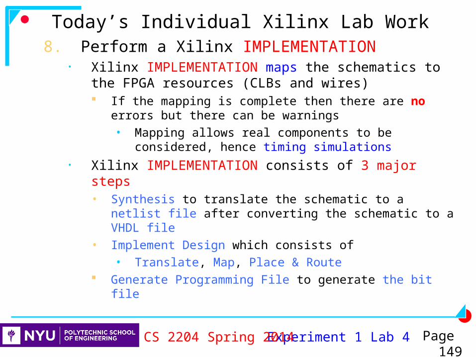
• Xilinx IMPLEMENTATION maps the schematics to the FPGA resources (CLBs and wires) If the mapping is complete then there are no errors but
there can be warnings• Mapping allows real components to be considered,
hence timing simulations• Xilinx IMPLEMENTATION consists of 3 major steps
• Synthesis to translate the schematic to a netlist file after converting the schematic to a VHDL file
• Implement Design which consists of• Translate, Map, Place & Route
Generate Programming File to generate the bit file
Experiment 1 Lab 4CS 2204 Spring 2014 Page 149

Today’s Individual Xilinx Lab Work8. Perform a Xilinx IMPLEMENTATION
Click on Design Summary (out of date) to be able to see number of errors and warnings
Right click on Generate Programming File and select Rerun All We will do the Synthesis, Implement Design and Generate Programming
File steps altogether• Even though we already did the synthesis, we will do it again to get
practice on this as we will do it many times• The question mark next to ppm1.sch is changed to a check
mark Wait until the IMPLEMENTATION completes
• If it does not complete, it stops at one of the steps We have to read the errors to read on the Design Summary panel
Once completed, there are no marks next to any one of the steps just performed
See the Project Navigator window on the next slide
Experiment 1 Lab 4CS 2204 Spring 2014 Page 150

Today’s Individual Xilinx Lab Work8. Perform a Xilinx IMPLEMENTATION
The Project Navigatorwindow looks like this after the IMPLEMENTATION is completed successfully :
Experiment 1 Lab 4CS 2204 Spring 2014 Page 151

Today’s Individual Xilinx Lab Work8. Perform a Xilinx IMPLEMENTATION
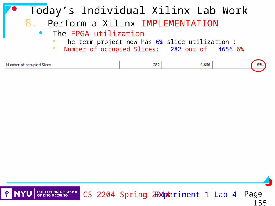
For the current IMPLEMENTATION we will get 0 Errors 66 Warnings one higher than the termproject project due
to the wire unused in Block 2 : XLXN_88 6% Slice utilization
Read the warnings by clicking on 66 Warnings on the Design Summary window whether or not the Xilinx IMPLEMENTATION completes
• We often check Design Summar yfor the warnings and the FPGA utilization
• Most warnings we check are in the Synthesis section• The FPGA utilization is lower than expected if there
are errors or warnings that must be corrected In Experiment 1, the number of warnings will be 66
This number will change depending on the experiment
Experiment 1 Lab 4CS 2204 Spring 2014 Page 152

Today’s Individual Xilinx Lab Work8. Perform a Xilinx IMPLEMENTATION
The IMPLEMENTATION warnings Why do we have 66 not 65 ?
• The termproject had only 65 warnings !• There is a new warning !• It is because a wire in Block 2 is not used
This wire is the wire that connected the “G” input of the Xilinx MUX to the GND in Block 2
Experiment 1 Lab 4CS 2204 Spring 2014 Page 153
This warning is OKWe will ignore it
Xst:646 - Signal <XLXN_88> is assigned but never used. This unconnected signal will be trimmed during the optimization process.

Today’s Individual Xilinx Lab Work8. Perform a Xilinx IMPLEMENTATION
The IMPLEMENTATION warnings How can I search for this wire in the schematics ?
• Press Ctrl-F or Click Edit -> Find…• When the Find window pops up select Nets on What• Enter XLXN_88 in the Net Name area• Click Find• The software will automatically switch to Block 2 and
show the wire in yellow• It is indeed the wire that connected GND to the deleted
MUX• We can ignore this wire• Close the window
Experiment 1 Lab 4CS 2204 Spring 2014 Page 154
Today’s Individual Xilinx Lab Work8. Perform a Xilinx IMPLEMENTATION
The FPGA utilization The term project now has 6% slice utilization : Number of occupied Slices: 282 out of 4656 6%
Experiment 1 Lab 4CS 2204 Spring 2014 Page 155

Today’s Individual Xilinx Lab Work9. Download the Ppm project to the FPGA chip
and play the game and to verify that the schematic works correctly
Program the FPGA chip Test the Ppm to see if it is working
• The developed 4-bit MUX handles the leftmost display If push button BTN4 is not pressed, it shows the position displays,
i.e. the random digit plays If push button BTN4 is pressed, it shows the leftmost Hex digit of
Player 2 points• Play the game on the FPGA board
If it does not work, inspect your circuit in Block 3 and correct the circuit
If you are sure your circuit is correct then• Compare your design with the Term Project Check List
handout to see if your design follows the handout• If yes, copy your Experiment 1 folder from the S drive and
to your laptop
Experiment 1 Lab 4CS 2204 Spring 2014 Page 156

Today’s Individual Xilinx Lab Work10. Help your partners complete today’s project
11. Submit your exp1 project once everyone completes the design
If all the team members have finished the 4-bit MUX design (Step 9 on the previous slide), they will decide whose project will be submitted
Students will fill out a Term Project Check List handout so that feedback can be given to them by the grading TAs
Students will signal to a TA who will copy their project
Experiment 1 Lab 4CS 2204 Spring 2014 Page 157

Today’s Individual Xilinx Lab Work12. Continue Reading the Term Project handout
Study and play the other two types of the Ppm game to think more about the our machine player’s strategy
Human vs. human : ppmhvsh Machine vs. machine : ppmmvsm
• Think about the playing strategy of the machine player that will be designed
Make sure you refresh your memory about the game rules and how to play the game
Also read slides at the end to learn about the software, Project Manager, Schematic design and other related topics
Experiment 1 Lab 4CS 2204 Spring 2014 Page 158

Understand Critical WiresRD : 4 bits
The random digitR1D : 4 bits
Next random digitR2D : 4 bits
The random digit after next random digitDISP : 16 bits
They represent the four position displays In Hex
DISP15-DISP12 : The leftmost position display, PD3 DISP11-DISP8 : position display PD2, etc
NPDISP : 16 bits The result of RD to each display digit
In Hex NPDISP15-NPDISP12 : The leftmost position, PD3, value + RD NPDISP11-NPDISP8 : Position display PD2 value + RD
NPSELDISP : 4 bits Selects one of NPDISP display values
In Hex
Experiment 1 Lab 4CS 2204 Spring 2014 Page 159

Understand Critical WiresBRWD : 4 bits
Basic reward In Hex
The digit played and also minimum points earned It is selected from RD or NPSELDISP
Based on how the player played : Directly or with an addition
Brwdeqz : 1 bit BRWD is zero when it is 1
PDPRD : 4 bits Display overflow bits after addition
Pdprd : 1 bitThe display overflow bit of the position played
Selplyr : 1 bit The current player
If it is 0, it is the human player, otherwise, it is the machine player
Experiment 1 Lab 4CS 2204 Spring 2014 Page 160

Understand Critical WiresP1SEL : 4 bits
The position played by the human playerP2SEL : 4 bits
The position played by the machine playerPSEL : 4 bits
Position Select bits of current playerENCPSEL : 2 bits
The number of the position playedEQ : 4 bits
The equality of the four displays to the digit playedNSD : 2 bits
The number of similar digits, i.e. the adjacency information of the position played
RWD : 8 bits The regular reward points calculated based on adjacencies
In Unsigned Binary CODERWD : 8 bits
The code reward points calculated based on the code digits In Unsigned Binary
Experiment 1 Lab 4CS 2204 Spring 2014 Page 161

Understand Critical WiresP1PT : 8 bits
Player 1 points In Hex
P2PT : 8 bits Player 2 points
In Hex
PT : 8 bits The points of the current player
In Hex
NPT : 8 bits New player points for the current player
In Hex
Ptovf : 1 bitThe points overflow
if it is 1, the new player points is above (255)10
Experiment 1 Lab 4CS 2204 Spring 2014 Page 162

Understand Critical WiresP1add : 1 bit
Player 1 adds when it is 1
P2add : 1 bit Player 2 adds when it is 1
Add : 1 bit The current player adds when it is 1
P1skip : 1 bit Player 1 skips when it is 1
P2skip : 1 bit Player 2 skips when it is 1
P1played : 1 bit Player 1 has played when it is 1
P2played : 1 bit Player 2 has played when it is 1
Experiment 1 Lab 4CS 2204 Spring 2014 Page 163

Understand Critical WiresDISPSEL : 2 bit
Selects one of four values for displays 00 Selects position displays (displays that RD is played on) 01 Selects player points 10 Selects next two random digits 11 Selects discovered code digits
Add : 1 bitShows that the current player has selected to add
Stp1pt : 1 bit Store Player 1 points
Stp2pt : 1 bit Store Player 2 points
Grd : 1 bit Signals to generate a new random digit
The random digit counter output is stored as P2RD while P2RD and P1RD are shifted to generate the new P1RD and RD
Bpds : 1 bitBlink one or all displays slowly
Bpdf : 1 bitBlocks a display fast after a display overflow
Experiment 1 Lab 4CS 2204 Spring 2014 Page 164

Understand Critical WiresClear : 1 bit
Clear FFs, registers, counters, etc. during reset in Block 2, Block 4 and Block 6 so that it can play again
Clearp2ffs : 1 bit Clears Player 2 FFs, counters and registers
Clff : 1 bit Clears FFs in Block 2 so that the next player can play if there is
no overflowS1 : 1 bit
State 1 where when it is 1, the Ppm is in state 1P2sturn : 1 bit
Signals that Player 2 has the turn It is 1 when the Ppm is in state 4
Sysclk : 1 bit System clock of the operation diagram at 6 Hz
P2clk : 1 bit The clock signal of Player 2 at 48 Hz
Rdclk : 1 bit The random digit counter clock at 192 Hz
Experiment 1 Lab 4CS 2204 Spring 2014 Page 165