Embed Size (px)
DESCRIPTION
AS1130 Datasheet en v5
Citation preview

austriamicrosystems AG
is now
ams AG The technical content of this austriamicrosystems datasheet is still valid.
Contact information:
Headquarters: ams AG
Tobelbaderstrasse 30
8141 Unterpremstaetten, Austria
Tel: +43 (0) 3136 500 0
e-Mail: [email protected]
Please visit our website at www.ams.com
Datasheet
AS1130 132-LED Cross-P lex ing Dr iver w i th scro l l ing Funct ion
lid
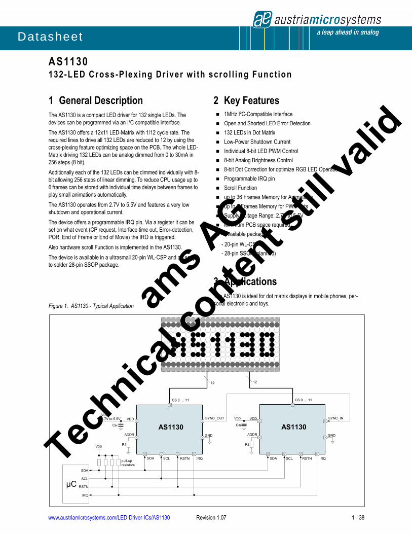
1 General DescriptionThe AS1130 is a compact LED driver for 132 single LEDs. The
devices can be programmed via an I²C compatible interface.
The AS1130 offers a 12x11 LED-Matrix with 1/12 cycle rate. The
required lines to drive all 132 LEDs are reduced to 12 by using the
cross-plexing feature optimizing space on the PCB. The whole LED-
Matrix driving 132 LEDs can be analog dimmed from 0 to 30mA in
256 steps (8 bit).
Additionally each of the 132 LEDs can be dimmed individually with 8-
bit allowing 256 steps of linear dimming. To reduce CPU usage up to
6 frames can be stored with individual time delays between frames to
play small animations automatically.
The AS1130 operates from 2.7V to 5.5V and features a very low
shutdown and operational current.
The device offers a programmable IRQ pin. Via a register it can be
set on what event (CP request, Interface time out, Error-detection,
POR, End of Frame or End of Movie) the IRO is triggered.
Also hardware scroll Function is implemented in the AS1130.
The device is available in a ultrasmall 20-pin WL-CSP and an easy
to solder 28-pin SSOP package.
Figure 1. AS1130 - Typical Application
2 Key Features 1MHz I²C-Compatible Interface
Open and Shorted LED Error Detection
132 LEDs in Dot Matrix
Low-Power Shutdown Current
Individual 8-bit LED PWM Control
8-bit Analog Brightness Control
8-bit Dot Correction for optimize RGB LED Operation
Programmable IRQ pin
Scroll Function
up to 36 Frames Memory for Animations
up to 6 Frames Memory for PWM sets
Supply Voltage Range: 2.7V to 5.5V
Minimum PCB space required
Available packages:
- 20-pin WL-CSP
- 28-pin SSOP (planned)
3 Applications
The AS1130 is ideal for dot matrix displays in mobile phones, per-
sonal electronic and toys.ams A
G
Technica
l conten
t still
va
www.austriamicrosystems.com/LED-Driver-ICs/AS1130 Revision 1.07 1 - 38
AS1130
Datasheet - P in o u t
lid
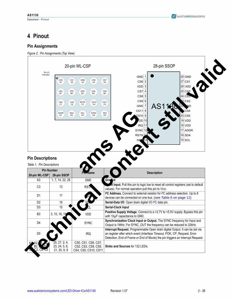
4 Pinout
Pin Assignments
Figure 2. Pin Assignments (Top View)
Pin Descriptions
Table 1. Pin Descriptions
Pin NumberPin Name Description
20-pin WL-CSP 28-pin SSOP
A3 1, 7, 14, 22, 28 GND Ground
C3 13 RSTNReset Input. Pull this pin to logic low to reset all control registers (set to default
values). For normal operation pull this pin to VDD.
D1 17 ADDRI²C Address. Connect to external resistor for I²C address selection. Up to 8
devices can be connected on one bus. (see Table 6 on page 12)D2 16 SDA Serial-Data I/O. Open drain digital I/O I²C data pin.
D3 15 SCL Serial-Clock Input
B3 3, 10, 18, 19, 26 VDDPositive Supply Voltage. Connect to a +2.7V to +5.5V supply. Bypass this pin
with 10µF capacitance to GND.
D4 12 SYNCSynchronization Clock Input or Output. The SYNC frequency for Input and
Output is 1MHz. For SYNC_OUT the frequency can be reduced to 32kHz.
D5 11 IRQ
Interrupt Request. Programmable Open drain digital Output. It can be set via
an register after which event (Interface Timeout, POK, CP_Request, Error
Detection, End of Frame or End of Movie) the pin triggers an Interrupt Request.
A1, A2, A4, A5, B1, B2, B4, B5, C1, C2, C4, C5
25, 27, 2, 4,23, 24, 5, 6,21, 20, 9, 8
CS0, CS1, CS6, CS7,CS2, CS3, CS8, CS9,
CS4, CS5, CS10, CS11Sinks and Sources for 132 LEDs.
20-pin WL-CSP 28-pin SSOP
ams A
G
Technica
l conten
t still
va
www.austriamicrosystems.com/LED-Driver-ICs/AS1130 Revision 1.07 2 - 38

AS1130
Datasheet - A bs o lu t e M ax i m um R a t i n gs
lid
5 Absolute Maximum Ratings
Stresses beyond those listed in Table 2 may cause permanent damage to the device. These are stress ratings only, and functional operation of
the device at these or any other conditions beyond those indicated in Section 6 Electrical Characteristics on page 4 is not implied.
Exposure to absolute maximum rating conditions for extended periods may affect device reliability.
Table 2. Absolute Maximum Ratings
Parameter Min Max Units Comments
Electrical Parameters
VDD to GND -0.3 7 V
All other pins to GND -0.37 or
VDD + 0.3V
Sink Current 500 mA
Segment Current 100 mA
Input Current (latch-up immunity) -100 100 mA Norm: JEDEC 78
Electrostatic Discharge
Electrostatic Discharge HBM 2 kV Norm: MIL 883 E method 3015
Temperature Ranges and Storage Conditions
Junction Temperature +150 ºC
Storage Temperature Range-55 +125 ºC for 20-pin WL-CSP
-55 +150 ºC for 28-pin SSOP
Package Body Temperature +260 ºC
The reflow peak soldering temperature (body temperature) specified is in accordance with IPC/JEDEC J-STD-020“Moisture/Reflow Sensitivity Classification for Non-Hermetic Solid State Surface Mount Devices”.
The lead finish for Pb-free leaded packages is matte tin (100% Sn).
Humidity non-condensing 5 85 %
Moisture Sensitive Level
120-pin
WL-CSPRepresents a max. floor life time of unlimited
328-pin SSOP
Represents a max. floor life time of 168h
ams A
G
Technica
l conten
t still
va
www.austriamicrosystems.com/LED-Driver-ICs/AS1130 Revision 1.07 3 - 38
AS1130
Datasheet - E le c t r i ca l C h a ra c t e r i s t i c s
lid
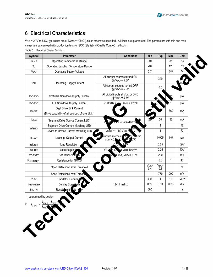
6 Electrical Characteristics
VDD = 2.7V to 5.5V, typ. values are at TAMB = +25ºC (unless otherwise specified). All limits are guaranteed. The parameters with min and max
values are guaranteed with production tests or SQC (Statistical Quality Control) methods.
Table 3. Electrical Characteristics
Symbol Parameter Conditions Min Typ Max Unit
TAMB Operating Temperature Range -40 85 °C
TJ Operating Junction Temperature Range -40 125 °C
VDD Operating Supply Voltage 2.7 5.5 V
IDD Operating Supply Current
All current sources turned ON@ VDD = 5.5V
340
mAAll current sources turned OFF
@ VDD = 5.5V0.5
IDDSSD Software Shutdown Supply Current All digital inputs at VDD or GND
@ VDD = 5.5V7 15 µA
IDDFSD Full Shutdown Supply Current Pin RSTN = 0V, TAMB = +25ºC 0.1 1 µA
IDIGITDigit Drive Sink Current
(Drive capability of all sources of one digit1)
1. guaranteed by design
360 mA
ISEG Segment Drive Source Current LED2
2.
VOUT = 1.8V to VDD-400mV28 30 32 mA
∆ISEGSegment Drive Current Matching LED 1 %
Device to Device Current Matching LED VOUT = 1.8V, VDD = 3.3V 1 %
ILEAK Leakage Output CurrentAll current sources OFF, VOUT = 0V,
VDD = 5.5V, TAMB = +25ºC0.005 0.5 µA
∆ILNR Line Regulation VOUT = 1.8V 0.25 %/V
∆ILDR Load Regulation VOUT = 1.8V to VDD-400mV 0.25 %/V
VDSSAT Saturation Voltage Current = 30mA, VDD = 3.3V 200 mV
RDSON(N) Resistance for NMOS 0.3 1 Ω
Open Detection Level ThresholdVDD-0.4
VDD-0.1
V
Short Detection Level Threshold 770 900 mV
fOSC Oscillator Frequency 0.9 1 1.1 MHz
fREFRESH Display Scan Rate 12x11 matrix 0.29 0.33 0.36 kHz
tRSTN Reset Pulse Width Low 500 ns
ISEG
Imax Imin–
Imax Imin+--------------------------- 100×=
ams A
G
Technica
l conten
t still
va
www.austriamicrosystems.com/LED-Driver-ICs/AS1130 Revision 1.07 4 - 38
AS1130
Datasheet - E le c t r i ca l C h a ra c t e r i s t i c s
lid
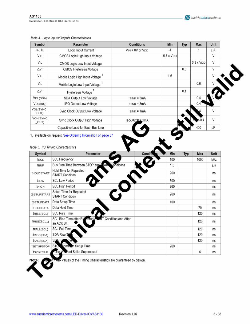
Note: The Min / Max values of the Timing Characteristics are guaranteed by design.
Table 4. Logic Inputs/Outputs Characteristics
Symbol Parameter Conditions Min Typ Max Unit
IIH, IIL Logic Input Current VIN = 0V or VDD -1 1 µA
VIH CMOS Logic High Input Voltage 0.7 x VDD V
VIL CMOS Logic Low Input Voltage 0.3 x VDD V
∆VI CMOS Hysteresis Voltage 0.3 V
VIH Mobile Logic High Input Voltage 1 1.6 V
VIL Mobile Logic Low Input Voltage 1 0.6 V
∆VI Hysteresis Voltage 1 0.1 V
VOL(SDA) SDA Output Low Voltage ISINK = 3mA 0.4 V
VOL(IRQ) IRQ Output Low Voltage ISINK = 3mA 0.4 V
VOL(SYNC_OUT)
Sync Clock Output Low Voltage ISINK = 1mA 0.4 V
VOH(SYNC_OUT) Sync Clock Output High Voltage ISOURCE = 1mA VDD-0.4 V
Capacitive Load for Each Bus Line 400 pF
1. available on request, See Ordering Information on page 37
Table 5. I²C Timing Characteristics
Symbol Parameter Conditions Min Typ Max Unit
fSCL SCL Frequency 100 1000 kHz
tBUF Bus Free Time Between STOP and START Conditions 1.3 µs
tHOLDSTARTHold Time for Repeated
START Condition260 ns
tLOW SCL Low Period 500 ns
tHIGH SCL High Period 260 ns
tSETUPSTARTSetup Time for Repeated
START Condition260 ns
tSETUPDATA Data Setup Time 100 ns
tHOLDDATA Data Hold Time 70 ns
tRISE(SCL) SCL Rise Time 120 ns
tRISE(SCL1)SCL Rise Time after Repeated START Condition and After
an ACK Bit120 ns
tFALL(SCL) SCL Fall Time 120 ns
tRISE(SDA) SDA Rise Time 120 ns
tFALL(SDA) SDA Fall Time 120 ns
tSETUPSTOP STOP Condition Setup Time 260 ns
tSPIKESUP Pulse Width of Spike Suppressed 6 ns
ams A
G
Technica
l conten
t still
va
www.austriamicrosystems.com/LED-Driver-ICs/AS1130 Revision 1.07 5 - 38

AS1130
Datasheet - E le c t r i ca l C h a ra c t e r i s t i c s
lid
Figure 3. Timing Diagram
Repeated START
SDI
SCL
STARTSTOP
tBUF
tLOW
tHOLDSTART
tHOLDDATA
tR
tHIGH
tFtSETUPDATA
tHOLDSTART
tSPIKESUP
tSETUPSTOP
tSETUPSTART
ams A
G
Technica
l conten
t still
va
www.austriamicrosystems.com/LED-Driver-ICs/AS1130 Revision 1.07 6 - 38
AS1130
Datasheet - Ty p i ca l O p e r a t i n g C h a r a c t e r i s t i c s
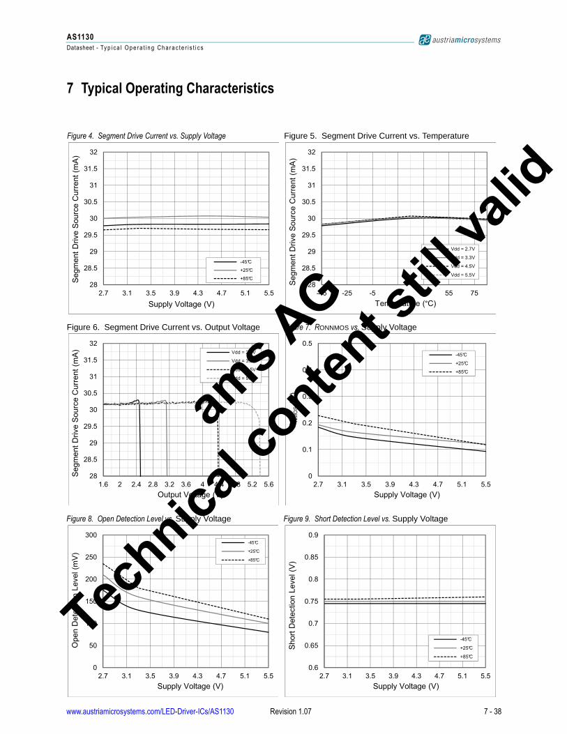
7 Typical Operating Characteristics
lid
Figure 4. Segment Drive Current vs. Supply Voltage Figure 5. Segment Drive Current vs. Temperature28
28.5
29
29.5
30
30.5
31
31.5
32
2.7 3.1 3.5 3.9 4.3 4.7 5.1 5.5
Segm
ent
Drive S
ourc
e C
urr
ent
(mA
)
Supply Voltage (V)
-45°C
+25°C
+85°C
28
28.5
29
29.5
30
30.5
31
31.5
32
-45 -25 -5 15 35 55 75S
egm
ent
Drive S
ourc
e C
urr
ent
(mA
)
Temperature (C)
Vdd = 2.7V
Vdd = 3.3V
Vdd = 4.5V
Vdd = 5.5V
G still v
a
Figure 6. Segment Drive Current vs. Output Voltage Figure 7. RONNMOS vs. Supply Voltage
28
28.5
29
29.5
30
30.5
31
31.5
32
1.6 2 2.4 2.8 3.2 3.6 4 4.4 4.8 5.2 5.6
Segm
ent
Drive S
ourc
e C
urr
ent
(mA
)
Output Voltage (V)
Vdd = 2.7V
Vdd = 3.3V
Vdd = 4.5V
Vdd = 5.5V
0
0.1
0.2
0.3
0.4
0.5
2.7 3.1 3.5 3.9 4.3 4.7 5.1 5.5
RN
MO
S(Ω
)
Supply Voltage (V)
-45°C
+25°C
+85°C
ams A
al co
ntent
Figure 8. Open Detection Level vs. Supply Voltage Figure 9. Short Detection Level vs. Supply Voltage
0
50
100
150
200
250
300
2.7 3.1 3.5 3.9 4.3 4.7 5.1 5.5
Open D
ete
ction L
evel (m
V)
Supply Voltage (V)
-45°C
+25°C
+85°C
0.6
0.65
0.7
0.75
0.8
0.85
0.9
2.7 3.1 3.5 3.9 4.3 4.7 5.1 5.5
Short
Dete
ction L
evel (V
)
Supply Voltage (V)
-45°C
+25°C
+85°C
Technic
www.austriamicrosystems.com/LED-Driver-ICs/AS1130 Revision 1.07 7 - 38
AS1130
Datasheet - Ty p i ca l O p e r a t i n g C h a r a c t e r i s t i c s
lid
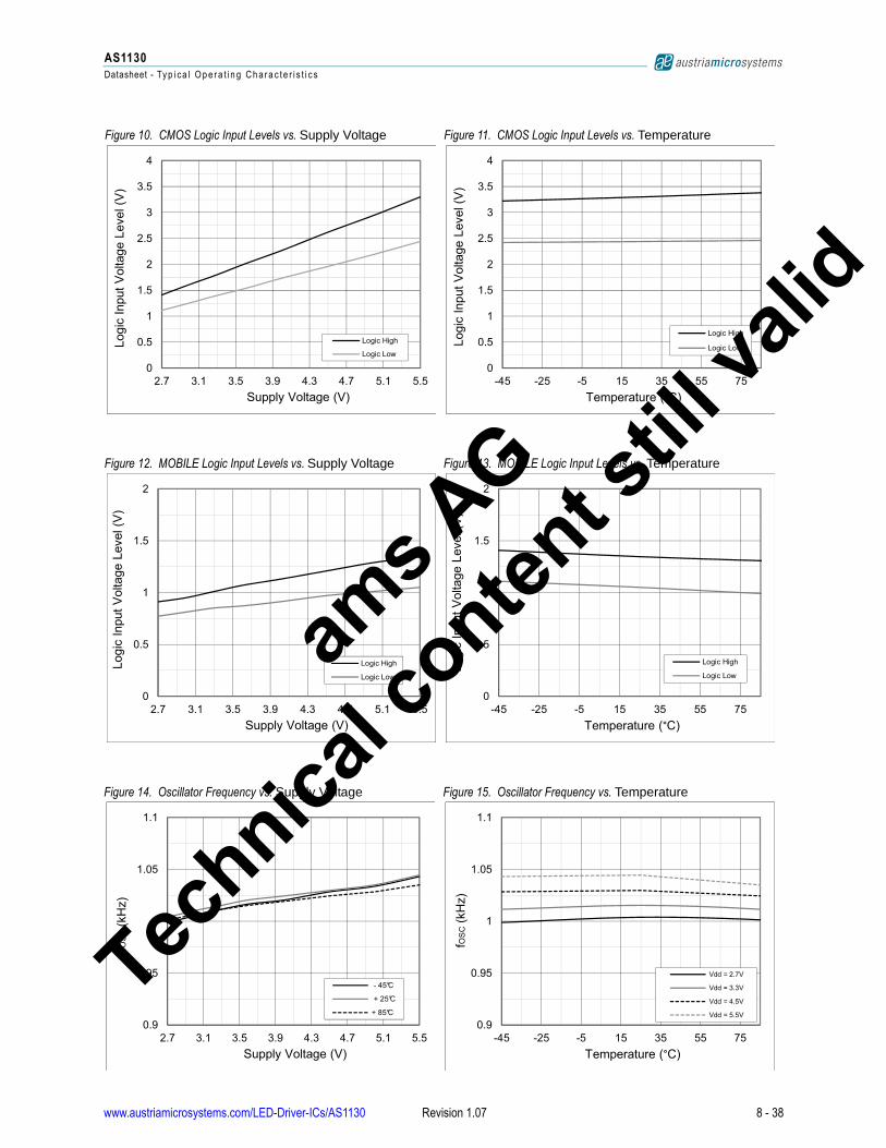
Figure 10. CMOS Logic Input Levels vs. Supply Voltage Figure 11. CMOS Logic Input Levels vs. Temperature
0
0.5
1
1.5
2
2.5
3
3.5
4
2.7 3.1 3.5 3.9 4.3 4.7 5.1 5.5
Logic
Input
Voltage L
evel (V
)
Supply Voltage (V)
Logic High
Logic Low
0
0.5
1
1.5
2
2.5
3
3.5
4
-45 -25 -5 15 35 55 75
Logic
Input
Voltage L
evel (V
)
Temperature (C)
Logic High
Logic Low
ill va
Figure 12. MOBILE Logic Input Levels vs. Supply Voltage Figure 13. MOBILE Logic Input Levels vs. Temperature
0
0.5
1
1.5
2
2.7 3.1 3.5 3.9 4.3 4.7 5.1 5.5
Logic
Input
Voltage L
evel (V
)
Supply Voltage (V)
Logic High
Logic Low
0
0.5
1
1.5
2
-45 -25 -5 15 35 55 75
Logic
Input
Voltage L
evel (V
)
Temperature (C)
Logic High
Logic Low
ams A
G
l conten
t st
Figure 14. Oscillator Frequency vs. Supply Voltage Figure 15. Oscillator Frequency vs. Temperature
0.9
0.95
1
1.05
1.1
2.7 3.1 3.5 3.9 4.3 4.7 5.1 5.5
fOS
C(k
Hz)
Supply Voltage (V)
- 45°C
+ 25°C
+ 85°C
0.9
0.95
1
1.05
1.1
-45 -25 -5 15 35 55 75
fOS
C(k
Hz)
Temperature (C)
Vdd = 2.7V
Vdd = 3.3V
Vdd = 4.5V
Vdd = 5.5V
Technica
www.austriamicrosystems.com/LED-Driver-ICs/AS1130 Revision 1.07 8 - 38
AS1130
Datasheet - D e t a i l e d D es c r i p t i o n
lid
8 Detailed Description
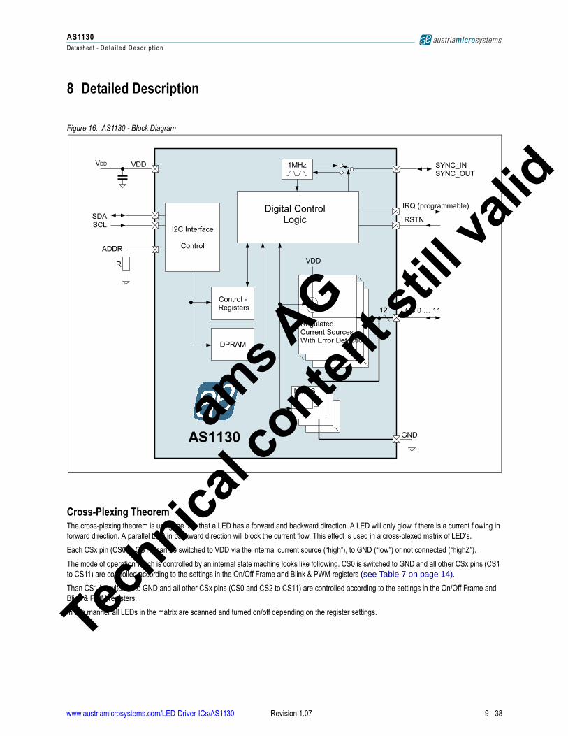
Figure 16. AS1130 - Block Diagram
Cross-Plexing TheoremThe cross-plexing theorem is using the fact that a LED has a forward and backward direction. A LED will only glow if there is a current flowing in
forward direction. A parallel LED in backward direction will block the current flow. This effect is used in a cross-plexed matrix of LED’s.
Each CSx pin (CS0 to CS11) can be switched to VDD via the internal current source (“high”), to GND (“low”) or not connected (“highZ”).
The mode of operation which is controlled by an internal state machine looks like following. CS0 is switched to GND and all other CSx pins (CS1
to CS11) are controlled according to the settings in the On/Off Frame and Blink & PWM registers (see Table 7 on page 14).
Than CS1 is switched to GND and all other CSx pins (CS0 and CS2 to CS11) are controlled according to the settings in the On/Off Frame and
Blink & PWM registers.
In this manner all LEDs in the matrix are scanned and turned on/off depending on the register settings.
ams A
G
Technica
l conten
t still
va
www.austriamicrosystems.com/LED-Driver-ICs/AS1130 Revision 1.07 9 - 38
AS1130
Datasheet - D e t a i l e d D es c r i p t i o n
lid
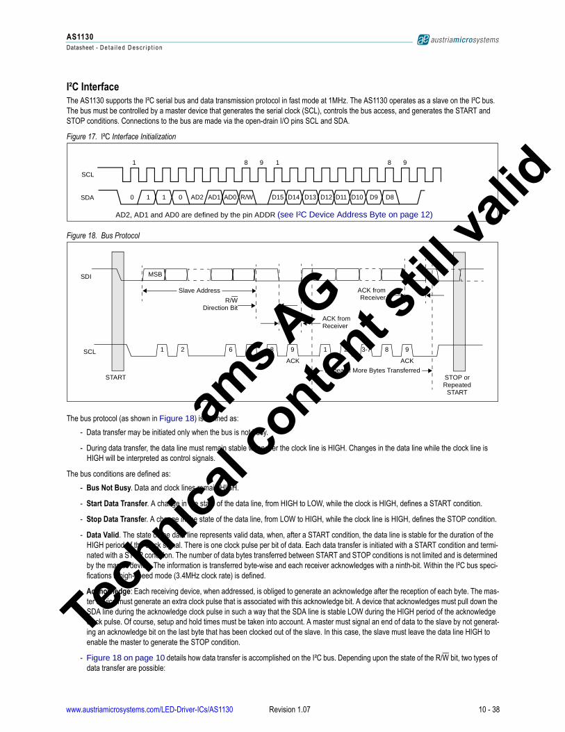
I²C InterfaceThe AS1130 supports the I²C serial bus and data transmission protocol in fast mode at 1MHz. The AS1130 operates as a slave on the I²C bus.
The bus must be controlled by a master device that generates the serial clock (SCL), controls the bus access, and generates the START and
STOP conditions. Connections to the bus are made via the open-drain I/O pins SCL and SDA.
Figure 17. I²C Interface Initialization
Figure 18. Bus Protocol
The bus protocol (as shown in Figure 18) is defined as:
- Data transfer may be initiated only when the bus is not busy.
- During data transfer, the data line must remain stable whenever the clock line is HIGH. Changes in the data line while the clock line is
HIGH will be interpreted as control signals.
The bus conditions are defined as:
- Bus Not Busy. Data and clock lines remain HIGH.
- Start Data Transfer. A change in the state of the data line, from HIGH to LOW, while the clock is HIGH, defines a START condition.
- Stop Data Transfer. A change in the state of the data line, from LOW to HIGH, while the clock line is HIGH, defines the STOP condition.
- Data Valid. The state of the data line represents valid data, when, after a START condition, the data line is stable for the duration of the
HIGH period of the clock signal. There is one clock pulse per bit of data. Each data transfer is initiated with a START condition and termi-
nated with a STOP condition. The number of data bytes transferred between START and STOP conditions is not limited and is determined
by the master device. The information is transferred byte-wise and each receiver acknowledges with a ninth-bit. Within the I²C bus speci-
fications a high-speed mode (3.4MHz clock rate) is defined.
- Acknowledge: Each receiving device, when addressed, is obliged to generate an acknowledge after the reception of each byte. The mas-
ter device must generate an extra clock pulse that is associated with this acknowledge bit. A device that acknowledges must pull down the
SDA line during the acknowledge clock pulse in such a way that the SDA line is stable LOW during the HIGH period of the acknowledge
clock pulse. Of course, setup and hold times must be taken into account. A master must signal an end of data to the slave by not generat-
ing an acknowledge bit on the last byte that has been clocked out of the slave. In this case, the slave must leave the data line HIGH to
enable the master to generate the STOP condition.
- Figure 18 on page 10 details how data transfer is accomplished on the I²C bus. Depending upon the state of the R/W bit, two types of
data transfer are possible:
1 98 1 98
10 AD21 0 AD1 AD0 R/W D15 D14 D13 D12 D11 D10 D9 D8
AD2, AD1 and AD0 are defined by the pin ADDR (see I²C Device Address Byte on page 12)
SCL
SDA
SDI
SCL
Slave Address
R/WDirection Bit
START
1 2 6 7 8 9 1 2 3-7 8 9
ACK
MSB
Repeat if More Bytes TransferredSTOP or Repeated
START
ACK from Receiver
ACK fromReceiver
ACK
ams A
G
Technica
l conten
t still
va
www.austriamicrosystems.com/LED-Driver-ICs/AS1130 Revision 1.07 10 - 38
AS1130
Datasheet - D e t a i l e d D es c r i p t i o n
lid
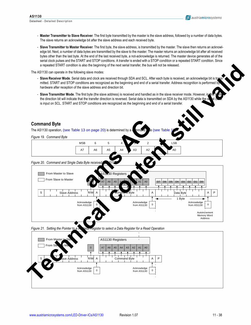
- Master Transmitter to Slave Receiver. The first byte transmitted by the master is the slave address, followed by a number of data bytes.
The slave returns an acknowledge bit after the slave address and each received byte.
- Slave Transmitter to Master Receiver. The first byte, the slave address, is transmitted by the master. The slave then returns an acknowl-
edge bit. Next, a number of data bytes are transmitted by the slave to the master. The master returns an acknowledge bit after all received
bytes other than the last byte. At the end of the last received byte, a not-acknowledge is returned. The master device generates all of the
serial clock pulses and the START and STOP conditions. A transfer is ended with a STOP condition or a repeated START condition. Since
a repeated START condition is also the beginning of the next serial transfer, the bus will not be released.
The AS1130 can operate in the following slave modes:
- Slave Receiver Mode. Serial data and clock are received through SDA and SCL. After each byte is received, an acknowledge bit is trans-
mitted. START and STOP conditions are recognized as the beginning and end of a serial transfer. Address recognition is performed by
hardware after reception of the slave address and direction bit.
- Slave Transmitter Mode. The first byte (the slave address) is received and handled as in the slave receiver mode. However, in this mode
the direction bit will indicate that the transfer direction is reversed. Serial data is transmitted on SDA by the AS1130 while the serial clock
is input on SCL. START and STOP conditions are recognized as the beginning and end of a serial transfer.
Command ByteThe AS1130 operation, (see Table 13 on page 20) is determined by a command byte (see Table 19).
Figure 19. Command Byte
Figure 20. Command and Single Data Byte received by AS1130
Figure 21. Setting the Pointer to a Address Register to select a Data Register for a Read Operation
A7 A6 A5 A4 A3 A2 A1 A0
MSB 6 5 4 3 2 1 LSB
From Master to Slave
From Slave to Master
A A PAS Command Byte Data ByteSlave Address
A6 A5 A4 A3 A2 A1 A0A7 D6 D5 D4 D3 D2 D1 D0D7
Acknowledgefrom AS11300 00
Acknowledgefrom AS1130
Acknowledgefrom AS1130
R/W
0
AS1130 Registers
Autoincrement Memory Word
Address
1 Byte
From Master to Slave
From Slave to Master
A PAS Command ByteSlave Address
A6 A5 A4 A3 A2 A1 A0A7
00Acknowledgefrom AS1130
Acknowledgefrom AS1130
R/W
0
AS1130 Registers
ams A
G
Technica
l conten
t still
va
www.austriamicrosystems.com/LED-Driver-ICs/AS1130 Revision 1.07 11 - 38
AS1130
Datasheet - D e t a i l e d D es c r i p t i o n
lid
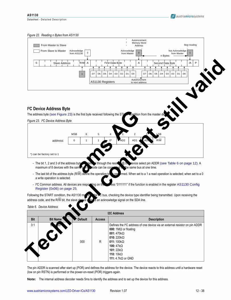
Figure 22. Reading n Bytes from AS1130
I²C Device Address ByteThe address byte (see Figure 23) is the first byte received following the START condition from the master device.
Figure 23. I²C Device Address Byte
- The bit 1, 2 and 3 of the address byte are defined through the resistor @ the device select pin ADDR (see Table 6 on page 12). A
maximum of 8 devices with the same pre-set code can be connected on the same bus at one time.
- The last bit of the address byte (R/W) define the operation to be performed. When set to a 1 a read operation is selected; when set to a 0
a write operation is selected.
- I²C Common address. All devices are responding on the address “0111111” if the function is enabled in the register AS1130 Config Register (0x06) on page 25.
Following the START condition, the AS1130 monitors the I²C bus, checking the device type identifier being transmitted. Upon receiving the
address code, and the R/W bit, the slave device outputs an acknowledge signal on the SDA line.
The pin ADDR is scanned after start up (POR) and defines the address for the device. The device reacts to this address until a hardware reset
(low on pin RSTN) is performed or the power-on-reset (POR) triggers again.
Note: The internal address decoder needs 5ms to identify the address and to set up the device for this address.
Table 6. Device Address
I2C Address
Bit Bit Name Default Access Description
3:1 i2c_addr
000 R
Defines the I²C address of one device via an external resistor on pin ADDR
000: 1MΩ or floating
001: 470kΩ010: 220kΩ011: 100kΩ100: 47kΩ101: 22kΩ110: 10kΩ111: 4.7kΩ or GND
From Master to Slave
From Slave to Master
A /A PAS First Data Byte Second Data ByteSlave Address
D6 D5 D4 D3 D2 D1 D0D7 D6 D5 D4 D3 D2 D1 D0D7
Not Acknowledgefrom Master0 10
Acknowledgefrom Master
Acknowledgefrom AS1130
R/W
1
AS1130 Registers
Autoincrement Memory Word
Address
n Bytes
Autoincrement to next address
Stop reading
0 1 1 0* AD2 AD1 AD0 R/W
MSB 6 5 4 3 2 1 LSB
address:
*) can be factory set to 1
ams A
G
Technica
l conten
t still
va
www.austriamicrosystems.com/LED-Driver-ICs/AS1130 Revision 1.07 12 - 38

AS1130
Datasheet - D e t a i l e d D es c r i p t i o n
lid
Initial Power-UpOn initial power-up, the AS1130 registers are reset to their default values, the display is blanked, and the device goes into shutdown mode. At
this time, all registers should be programmed for normal operation. To bring the device into normal operation the following sequence needs to be
performed.
Start-up sequence:- Power-up the AS1130 (connect VDD to a source), the devices is in shutdown;
- After 5ms the address of the AS1130 is valid and the first I²C command can be send.
- Define RAM Configuration; bit mem_conf in the AS1130 Config Register (see Table 20 on page 25) - On/Off Frames
- Blink & PWM Sets
- Dot Correction, if specified
- Define Control Register (see Table 13 on page 20) - Current Source
- Display options
- Display picture / play movie
- To light up the LEDs set the shdn bit to ‘1’ for normal operation mode (see Table 23 on page 26).
Shutdown ModeThe AS1130 device features two different shutdown modes. A software shutdown via shutdown register (see Shutdown & Open/Short Register Format on page 26) and a hardware shutdown via the RSTN pin.
The software shutdown disables all LED’s and stops the internal operation of the logic. A shutdown mode via the RSTN pin additionally powers
down the power-on-reset (POR) of the device. In this shutdown mode the AS1130 consumes only 100nA (typ.).
ams A
G
Technica
l conten
t still
va
www.austriamicrosystems.com/LED-Driver-ICs/AS1130 Revision 1.07 13 - 38
AS1130
Datasheet - R e g i s t e r D e s c r i p t i on
lid
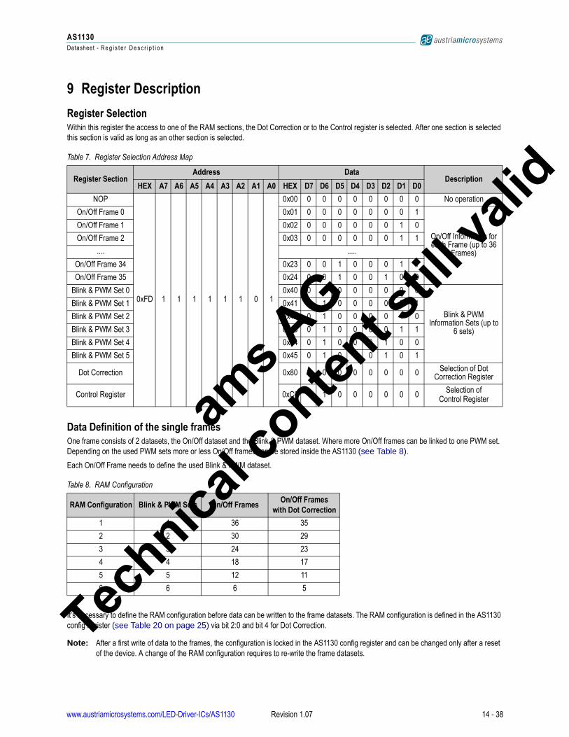
9 Register Description
Register SelectionWithin this register the access to one of the RAM sections, the Dot Correction or to the Control register is selected. After one section is selected
this section is valid as long as an other section is selected.
Data Definition of the single framesOne frame consists of 2 datasets, the On/Off dataset and the Blink & PWM dataset. Where more On/Off frames can be linked to one PWM set.
Depending on the used PWM sets more or less On/Off frames can be stored inside the AS1130 (see Table 8).
Each On/Off Frame needs to define the used Blink & PWM dataset.
It’s necessary to define the RAM configuration before data can be written to the frame datasets. The RAM configuration is defined in the AS1130
config register (see Table 20 on page 25) via bit 2:0 and bit 4 for Dot Correction.
Note: After a first write of data to the frames, the configuration is locked in the AS1130 config register and can be changed only after a reset
of the device. A change of the RAM configuration requires to re-write the frame datasets.
Table 7. Register Selection Address Map
Register SectionAddress Data
DescriptionHEX A7 A6 A5 A4 A3 A2 A1 A0 HEX D7 D6 D5 D4 D3 D2 D1 D0
NOP
0xFD 1 1 1 1 1 1 0 1
0x00 0 0 0 0 0 0 0 0 No operation
On/Off Frame 0 0x01 0 0 0 0 0 0 0 1
On/Off Information for each Frame (up to 36
Frames)
On/Off Frame 1 0x02 0 0 0 0 0 0 1 0
On/Off Frame 2 0x03 0 0 0 0 0 0 1 1
.... .....
On/Off Frame 34 0x23 0 0 1 0 0 0 1 1
On/Off Frame 35 0x24 0 0 1 0 0 1 0 0
Blink & PWM Set 0 0x40 0 1 0 0 0 0 0 0
Blink & PWM Information Sets (up to
6 sets)
Blink & PWM Set 1 0x41 0 1 0 0 0 0 0 1
Blink & PWM Set 2 0x42 0 1 0 0 0 0 1 0
Blink & PWM Set 3 0x43 0 1 0 0 0 0 1 1
Blink & PWM Set 4 0x44 0 1 0 0 0 1 0 0
Blink & PWM Set 5 0x45 0 1 0 0 0 1 0 1
Dot Correction 0x80 1 0 0 0 0 0 0 0Selection of Dot
Correction Register
Control Register 0xC0 1 1 0 0 0 0 0 0Selection of
Control Register
Table 8. RAM Configuration
RAM Configuration Blink & PWM Sets On/Off FramesOn/Off Frames
with Dot Correction
1 1 36 35
2 2 30 29
3 3 24 23
4 4 18 17
5 5 12 11
6 6 6 5
ams A
G
Technica
l conten
t still
va
www.austriamicrosystems.com/LED-Driver-ICs/AS1130 Revision 1.07 14 - 38
AS1130
Datasheet - R e g i s t e r D e s c r i p t i on
lid
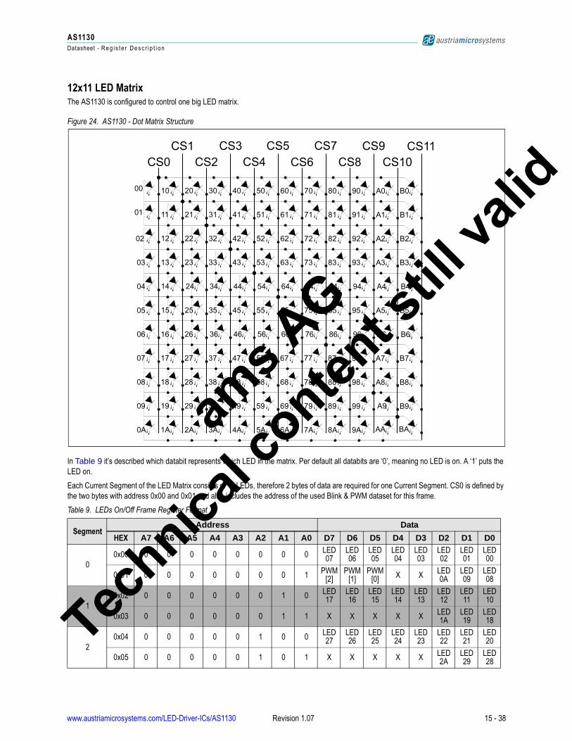
12x11 LED MatrixThe AS1130 is configured to control one big LED matrix.
Figure 24. AS1130 - Dot Matrix Structure
In Table 9 it’s described which databit represents which LED in the matrix. Per default all databits are ‘0’, meaning no LED is on. A ‘1’ puts the
LED on.
Each Current Segment of the LED Matrix consists of 11 LEDs, therefore 2 bytes of data are required for one Current Segment. CS0 is defined by
the two bytes with address 0x00 and 0x01 and also includes the address of the used Blink & PWM dataset for this frame.
Table 9. LEDs On/Off Frame Register Format
SegmentAddress Data
HEX A7 A6 A5 A4 A3 A2 A1 A0 D7 D6 D5 D4 D3 D2 D1 D0
0
0x00 0 0 0 0 0 0 0 0LED 07
LED 06
LED 05
LED 04
LED 03
LED 02
LED 01
LED 00
0x01 0 0 0 0 0 0 0 1PWM
[2]PWM
[1]PWM
[0]X X
LED 0A
LED 09
LED 08
1
0x02 0 0 0 0 0 0 1 0LED 17
LED 16
LED 15
LED 14
LED 13
LED 12
LED 11
LED 10
0x03 0 0 0 0 0 0 1 1 X X X X XLED 1A
LED 19
LED 18
2
0x04 0 0 0 0 0 1 0 0LED 27
LED 26
LED 25
LED 24
LED 23
LED 22
LED 21
LED 20
0x05 0 0 0 0 0 1 0 1 X X X X XLED 2A
LED 29
LED 28
ams A
G
Technica
l conten
t still
va
www.austriamicrosystems.com/LED-Driver-ICs/AS1130 Revision 1.07 15 - 38
AS1130
Datasheet - R e g i s t e r D e s c r i p t i on
lid
The Blink & PWM sets contain blink on/off and the digital PWM information for each LED in the matrix. The number of PWM datasets is flexible
according to the defined RAM configuration (see Figure 8 on page 14).
In the blink register (see Table 10) every single LED can be set to blink. The blink period is set in the display option register (see Display Option Register Format on page 24).
3
0x06 0 0 0 0 0 1 1 0LED 37
LED 36
LED 35
LED34
LED33
LED 32
LED 31
LED 30
0x07 0 0 0 0 0 1 1 1 X X X X XLED 3A
LED 39
LED 38
4
0x08 0 0 0 0 1 0 0 0LED 47
LED 46
LED 45
LED44
LED 43
LED 42
LED 41
LED 40
0x09 0 0 0 0 1 0 0 1 X X X X XLED 4A
LED 49
LED 48
5
0x0A 0 0 0 0 1 0 1 0LED 57
LED 56
LED 55
LED54
LED 53
LED 52
LED 51
LED 50
0x0B 0 0 0 0 1 0 1 1 X X X X XLED 5A
LED 59
LED 58
6
0x0C 0 0 0 0 1 1 0 0LED 67
LED 66
LED 65
LED64
LED 63
LED 62
LED 61
LED 60
0x0D 0 0 0 0 1 1 0 1 X X X X XLED 6A
LED 69
LED 68
7
0x0E 0 0 0 0 1 1 1 0LED 77
LED 76
LED 75
LED74
LED 73
LED 72
LED 71
LED 70
0x0F 0 0 0 0 1 1 1 1 X X X X XLED 7A
LED 79
LED 78
8
0x10 0 0 0 1 0 0 0 0LED 87
LED 86
LED 85
LED84
LED 83
LED 82
LED 81
LED 80
0x11 0 0 0 1 0 0 0 1 X X X X XLED 8A
LED 89
LED 88
9
0x12 0 0 0 1 0 0 1 0LED 97
LED 96
LED 95
LED94
LED 93
LED 92
LED 91
LED 90
0x13 0 0 0 1 0 0 1 1 X X X X XLED 9A
LED 99
LED 98
A
0x14 0 0 0 1 0 1 0 0LED A7
LED A6
LED A5
LEDA4
LED A3
LED A2
LED A1
LED A0
0x15 0 0 0 1 0 1 0 1 X X X X XLED AA
LED A9
LED A8
B
0x16 0 0 0 1 0 1 1 0LED B7
LED B6
LED B5
LEDB4
LED B3
LED B2
LED B1
LED B0
0x17 0 0 0 1 0 1 1 1 X X X X XLED BA
LED B9
LED B8
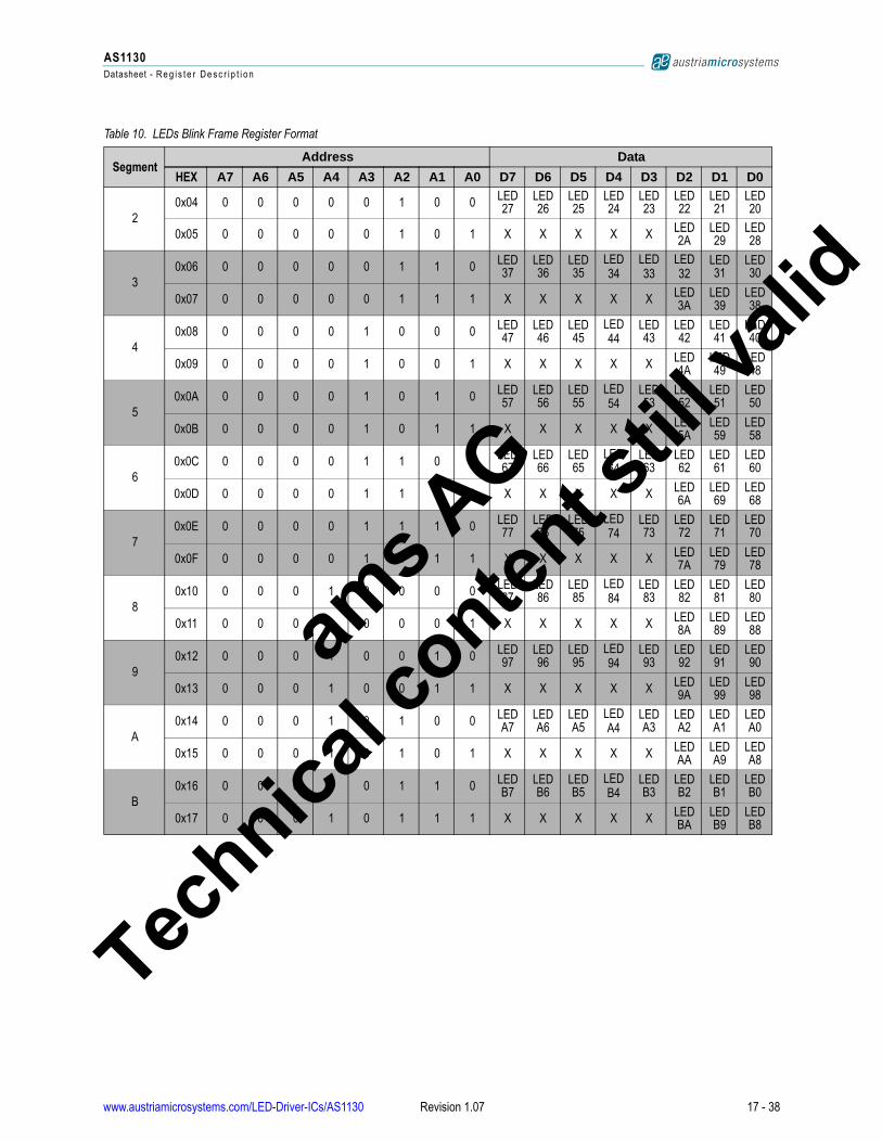
Table 10. LEDs Blink Frame Register Format
SegmentAddress Data
HEX A7 A6 A5 A4 A3 A2 A1 A0 D7 D6 D5 D4 D3 D2 D1 D0
0
0x00 0 0 0 0 0 0 0 0LED 07
LED 06
LED 05
LED 04
LED 03
LED 02
LED 01
LED 00
0x01 0 0 0 0 0 0 0 1 X X X X XLED 0A
LED 09
LED 08
1
0x02 0 0 0 0 0 0 1 0LED 17
LED 16
LED 15
LED 14
LED 13
LED 12
LED 11
LED 10
0x03 0 0 0 0 0 0 1 1 X X X X XLED 1A
LED 19
LED 18
Table 9. LEDs On/Off Frame Register Format
SegmentAddress Data
HEX A7 A6 A5 A4 A3 A2 A1 A0 D7 D6 D5 D4 D3 D2 D1 D0
ams A
G
Technica
l conten
t still
va
www.austriamicrosystems.com/LED-Driver-ICs/AS1130 Revision 1.07 16 - 38
AS1130
Datasheet - R e g i s t e r D e s c r i p t i on
lid
20x04 0 0 0 0 0 1 0 0LED 27
LED 26
LED 25
LED 24
LED 23
LED 22
LED 21
LED 20
0x05 0 0 0 0 0 1 0 1 X X X X XLED 2A
LED 29
LED 28
3
0x06 0 0 0 0 0 1 1 0LED 37
LED 36
LED 35
LED34
LED33
LED32
LED 31
LED 30
0x07 0 0 0 0 0 1 1 1 X X X X XLED 3A
LED 39
LED 38
4
0x08 0 0 0 0 1 0 0 0LED 47
LED 46
LED 45
LED44
LED 43
LED 42
LED 41
LED 40
0x09 0 0 0 0 1 0 0 1 X X X X XLED 4A
LED 49
LED 48
5
0x0A 0 0 0 0 1 0 1 0LED 57
LED 56
LED 55
LED54
LED 53
LED 52
LED 51
LED 50
0x0B 0 0 0 0 1 0 1 1 X X X X XLED 5A
LED 59
LED 58
6
0x0C 0 0 0 0 1 1 0 0LED 67
LED 66
LED 65
LED64
LED 63
LED 62
LED 61
LED 60
0x0D 0 0 0 0 1 1 0 1 X X X X XLED 6A
LED 69
LED 68
7
0x0E 0 0 0 0 1 1 1 0LED 77
LED 76
LED 75
LED74
LED 73
LED 72
LED 71
LED 70
0x0F 0 0 0 0 1 1 1 1 X X X X XLED 7A
LED 79
LED 78
8
0x10 0 0 0 1 0 0 0 0LED 87
LED 86
LED 85
LED84
LED 83
LED 82
LED 81
LED 80
0x11 0 0 0 1 0 0 0 1 X X X X XLED 8A
LED 89
LED 88
9
0x12 0 0 0 1 0 0 1 0LED 97
LED 96
LED 95
LED94
LED 93
LED 92
LED 91
LED 90
0x13 0 0 0 1 0 0 1 1 X X X X XLED 9A
LED 99
LED 98
A
0x14 0 0 0 1 0 1 0 0LED A7
LED A6
LED A5
LEDA4
LED A3
LED A2
LED A1
LED A0
0x15 0 0 0 1 0 1 0 1 X X X X XLED AA
LED A9
LED A8
B
0x16 0 0 0 1 0 1 1 0LED B7
LED B6
LED B5
LEDB4
LED B3
LED B2
LED B1
LED B0
0x17 0 0 0 1 0 1 1 1 X X X X XLED BA
LED B9
LED B8
Table 10. LEDs Blink Frame Register Format
SegmentAddress Data
HEX A7 A6 A5 A4 A3 A2 A1 A0 D7 D6 D5 D4 D3 D2 D1 D0
ams A
G
Technica
l conten
t still
va
www.austriamicrosystems.com/LED-Driver-ICs/AS1130 Revision 1.07 17 - 38

AS1130
Datasheet - R e g i s t e r D e s c r i p t i on
lid
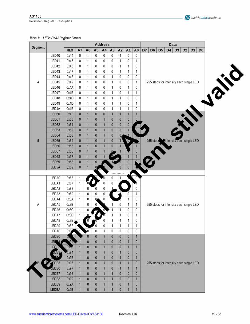
In the PWM register (see Table 11) the brightness of every single LED can be set via a 8bit PWM (255 steps).
Table 11. LEDs PWM Register Format
SegmentAddress Data
HEX A7 A6 A5 A4 A3 A2 A1 A0 D7 D6 D5 D4 D3 D2 D1 D0
0
LED00 0x18 0 0 0 1 1 0 0 0
255 steps for intensity each single LED
LED01 0x19 0 0 0 1 1 0 0 1
LED02 0x1A 0 0 0 1 1 0 1 0
LED03 0x1B 0 0 0 1 1 0 1 1
LED04 0x1C 0 0 0 1 1 1 0 0
LED05 0x1D 0 0 0 1 1 1 0 1
LED06 0x1E 0 0 0 1 1 1 1 0
LED07 0x1F 0 0 0 1 1 1 1 1
LED08 0x20 0 0 1 0 0 0 0 0
LED09 0x21 0 0 1 0 0 0 0 1
LED0A 0x22 0 0 1 0 0 0 1 0
1
LED10 0x23 0 0 1 0 0 0 1 1
255 steps for intensity each single LED
LED11 0x24 0 0 1 0 0 1 0 0
LED12 0x25 0 0 1 0 0 1 0 1
LED13 0x26 0 0 1 0 0 1 1 0
LED14 0x27 0 0 1 0 0 1 1 1
LED15 0x28 0 0 1 0 1 0 0 0
LED16 0x29 0 0 1 0 1 0 0 1
LED17 0x2A 0 0 1 0 1 0 1 0
LED18 0x2B 0 0 1 0 1 0 1 1
LED19 0x2C 0 0 1 0 1 1 0 0
LED1A 0x2D 0 0 1 0 1 1 0 1
2
LED20 0x2E 0 0 1 0 1 1 1 0
255 steps for intensity each single LED
LED21 0x2F 0 0 1 0 1 1 1 1
LED22 0x30 0 0 1 1 0 0 0 0
LED23 0x31 0 0 1 1 0 0 0 1
LED24 0x32 0 0 1 1 0 0 1 0
LED25 0x33 0 0 1 1 0 0 1 1
LED26 0x34 0 0 1 1 0 1 0 0
LED27 0x35 0 0 1 1 0 1 0 1
LED28 0x36 0 0 1 1 0 1 1 0
LED29 0x37 0 0 1 1 0 1 1 1
LED2A 0x38 0 0 1 1 1 0 0 0
3
LED30 0x39 0 0 1 1 1 0 0 1
255 steps for intensity each single LED
LED31 0x3A 0 0 1 1 1 0 1 0
LED32 0x3B 0 0 1 1 1 0 1 1
LED33 0x3C 0 0 1 1 1 1 0 0
LED34 0x3D 0 0 1 1 1 1 0 1
LED35 0x3E 0 0 1 1 1 1 1 0
LED36 0x3F 0 0 1 1 1 1 1 1
LED37 0x40 0 1 0 0 0 0 0 0
LED38 0x41 0 1 0 0 0 0 0 1
LED39 0x42 0 1 0 0 0 0 1 0
LED3A 0x43 0 1 0 0 0 0 1 1
ams A
G
Technica
l conten
t still
va
www.austriamicrosystems.com/LED-Driver-ICs/AS1130 Revision 1.07 18 - 38
AS1130
Datasheet - R e g i s t e r D e s c r i p t i on
lid
4LED40 0x44 0 1 0 0 0 1 0 0
255 steps for intensity each single LED
LED41 0x45 0 1 0 0 0 1 0 1
LED42 0x46 0 1 0 0 0 1 1 0
LED43 0x47 0 1 0 0 0 1 1 1
LED44 0x48 0 1 0 0 1 0 0 0
LED45 0x49 0 1 0 0 1 0 0 1
LED46 0x4A 0 1 0 0 1 0 1 0
LED47 0x4B 0 1 0 0 1 0 1 1
LED48 0x4C 0 1 0 0 1 1 0 0
LED49 0x4D 0 1 0 0 1 1 0 1
LED4A 0x4E 0 1 0 0 1 1 1 0
5
LED50 0x4F 0 1 0 0 1 1 1 1
255 steps for intensity each single LED
LED51 0x50 0 1 0 1 0 0 0 0
LED52 0x51 0 1 0 1 0 0 0 1
LED53 0x52 0 1 0 1 0 0 1 0
LED54 0x53 0 1 0 1 0 0 1 1
LED55 0x54 0 1 0 1 0 1 0 0
LED56 0x55 0 1 0 1 0 1 0 1
LED57 0x56 0 1 0 1 0 1 1 0
LED58 0x57 0 1 0 1 0 1 1 1
LED59 0x58 0 1 0 1 1 0 0 0
LED5A 0x59 0 1 0 1 1 0 0 1
................
A
LEDA0 0x86 1 0 0 0 0 1 1 0
255 steps for intensity each single LED
LEDA1 0x87 1 0 0 0 0 1 1 1
LEDA2 0x88 1 0 0 0 1 0 0 0
LEDA3 0x89 1 0 0 0 1 0 0 1
LEDA4 0x8A 1 0 0 0 1 0 1 0
LEDA5 0x8B 1 0 0 0 1 0 1 1
LEDA6 0x8C 1 0 0 0 1 1 0 0
LEDA7 0x8D 1 0 0 0 1 1 0 1
LEDA8 0x8E 1 0 0 0 1 1 1 0
LEDA9 0x8F 1 0 0 0 1 1 1 1
LEDA0 0x90 1 0 0 1 0 0 0 0
B
LEDB0 0x91 1 0 0 1 0 0 0 1
255 steps for intensity each single LED
LEDB1 0x92 1 0 0 1 0 0 1 0
LEDB2 0x93 1 0 0 1 0 0 1 1
LEDB3 0x94 1 0 0 1 0 1 0 0
LEDB4 0x95 1 0 0 1 0 1 0 1
LEDB5 0x96 1 0 0 1 0 1 1 0
LEDB6 0x97 1 0 0 1 0 1 1 1
LEDB7 0x98 1 0 0 1 1 0 0 0
LEDB8 0x99 1 0 0 1 1 0 0 1
LEDB9 0x9A 1 0 0 1 1 0 1 0
LEDBA 0x9B 1 0 0 1 1 0 1 1
Table 11. LEDs PWM Register Format
SegmentAddress Data
HEX A7 A6 A5 A4 A3 A2 A1 A0 D7 D6 D5 D4 D3 D2 D1 D0
ams A
G
Technica
l conten
t still
va
www.austriamicrosystems.com/LED-Driver-ICs/AS1130 Revision 1.07 19 - 38
AS1130
Datasheet - R e g i s t e r D e s c r i p t i on
lid
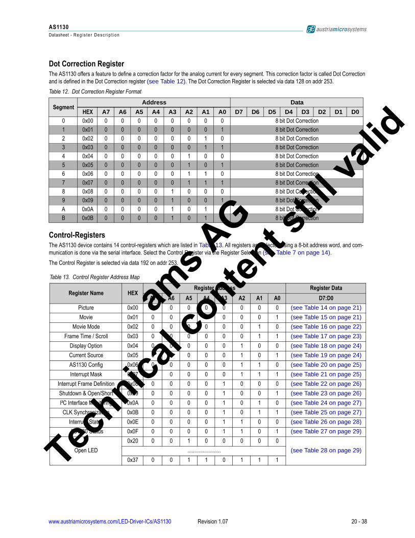
Dot Correction RegisterThe AS1130 offers a feature to define a correction factor for the analog current for every segment. This correction factor is called Dot Correction
and is defined in the Dot Correction register (see Table 12). The Dot Correction Register is selected via data 128 on addr 253.
Control-RegistersThe AS1130 device contains 14 control-registers which are listed in Table 13. All registers are selected using a 8-bit address word, and com-
munication is done via the serial interface. Select the Control Register via the Register Selection (see Table 7 on page 14).
The Control Register is selected via data 192 on addr 253.
Table 12. Dot Correction Register Format
SegmentAddress Data
HEX A7 A6 A5 A4 A3 A2 A1 A0 D7 D6 D5 D4 D3 D2 D1 D00 0x00 0 0 0 0 0 0 0 0 8 bit Dot Correction
1 0x01 0 0 0 0 0 0 0 1 8 bit Dot Correction
2 0x02 0 0 0 0 0 0 1 0 8 bit Dot Correction
3 0x03 0 0 0 0 0 0 1 1 8 bit Dot Correction
4 0x04 0 0 0 0 0 1 0 0 8 bit Dot Correction
5 0x05 0 0 0 0 0 1 0 1 8 bit Dot Correction
6 0x06 0 0 0 0 0 1 1 0 8 bit Dot Correction
7 0x07 0 0 0 0 0 1 1 1 8 bit Dot Correction
8 0x08 0 0 0 0 1 0 0 0 8 bit Dot Correction
9 0x09 0 0 0 0 1 0 0 1 8 bit Dot Correction
A 0x0A 0 0 0 0 1 0 1 0 8 bit Dot Correction
B 0x0B 0 0 0 0 1 0 1 1 8 bit Dot Correction
Table 13. Control Register Address Map
Register Name HEXRegister Address Register Data
A7 A6 A5 A4 A3 A2 A1 A0 D7:D0
Picture 0x00 0 0 0 0 0 0 0 0 (see Table 14 on page 21)
Movie 0x01 0 0 0 0 0 0 0 1 (see Table 15 on page 21)
Movie Mode 0x02 0 0 0 0 0 0 1 0 (see Table 16 on page 22)
Frame Time / Scroll 0x03 0 0 0 0 0 0 1 1 (see Table 17 on page 23)
Display Option 0x04 0 0 0 0 0 1 0 0 (see Table 18 on page 24)
Current Source 0x05 0 0 0 0 0 1 0 1 (see Table 19 on page 24)
AS1130 Config 0x06 0 0 0 0 0 1 1 0 (see Table 20 on page 25)
Interrupt Mask 0x07 0 0 0 0 0 1 1 1 (see Table 21 on page 25)
Interrupt Frame Definition 0x08 0 0 0 0 1 0 0 0 (see Table 22 on page 26)
Shutdown & Open/Short 0x09 0 0 0 0 1 0 0 1 (see Table 23 on page 26)
I²C Interface Monitoring 0x0A 0 0 0 0 1 0 1 0 (see Table 24 on page 27)
CLK Synchronization 0x0B 0 0 0 0 1 0 1 1 (see Table 25 on page 27)
Interrupt Status 0x0E 0 0 0 0 1 1 0 0 (see Table 26 on page 28)
AS1130 Status 0x0F 0 0 0 0 1 1 0 1 (see Table 27 on page 29)
Open LED
0x20 0 0 1 0 0 0 0 0
(see Table 28 on page 29)........................
0x37 0 0 1 1 0 1 1 1
ams A
G
Technica
l conten
t still
va
www.austriamicrosystems.com/LED-Driver-ICs/AS1130 Revision 1.07 20 - 38
AS1130
Datasheet - R e g i s t e r D e s c r i p t i on
lid
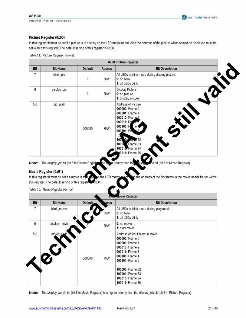
Picture Register (0x00)
In this register it must be set if a picture is to display on the LED matrix or not. Also the address of the picture which should be displayed must be
set withi n this register. The default setting of this register is 0x00.
Note: The display_pic bit (bit 6 in Picture Register) has lower priority than the display_movie bit (bit 6 in Movie Register).
Movie Register (0x01)
In this register it must be set if a movie is to display on the LED matrix or not. Also the address of the first frame in the movie needs be set within
this register. The default setting of this register is 0x00.
Note: The display_movie bit (bit 6 in Movie Register) has higher priority than the display_pic bit (bit 6 in Picture Register).
Table 14. Picture Register Format
0x00 Picture Register
Bit Bit Name Default Access Bit Description
7 blink_pic
0 R/W
All LEDs in blink mode during display picture
0: no blink
1: all LEDs blink
6 display_pic
0 R/W
Display Picture
0: no picture
1: display picture
5:0 pic_addr
000000 R/W
Address of Picture
000000: Frame 0
000001: Frame 1
000010: Frame 2
000011: Frame 3
000100: Frame 4
000101: Frame 5
...............
100000: Frame 32
100001: Frame 33
100010: Frame 34
100011: Frame 35
Table 15. Movie Register Format
0x01 Movie Register
Bit Bit Name Default Access Bit Description
7 blink_movie
0 R/W
All LEDs in blink mode during play movie
0: no blink
1: all LEDs blink
6 display_movie0 R/W
0: no movie
1: start movie
5:0 movie_addr
000000 R/W
Address of first Frame in Movie
000000: Frame 0
000001: Frame 1
000010: Frame 2
000011: Frame 3
000100: Frame 4
000101: Frame 5
...............
100000: Frame 32
100001: Frame 33
100010: Frame 34
100011: Frame 35
ams A
G
Technica
l conten
t still
va
www.austriamicrosystems.com/LED-Driver-ICs/AS1130 Revision 1.07 21 - 38
AS1130
Datasheet - R e g i s t e r D e s c r i p t i on
lid
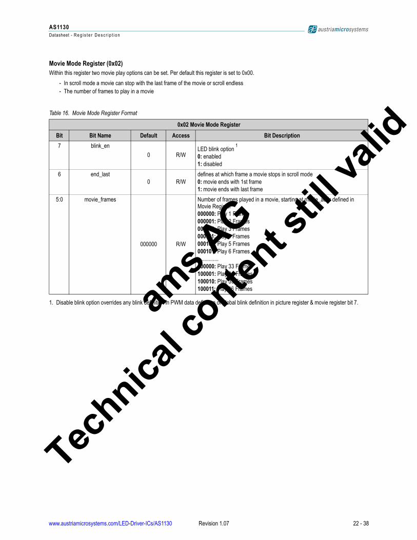
Movie Mode Register (0x02)
Within this register two movie play options can be set. Per default this register is set to 0x00.
- In scroll mode a movie can stop with the last frame of the movie or scroll endless
- The number of frames to play in a movie
Table 16. Movie Mode Register Format
0x02 Movie Mode Register
Bit Bit Name Default Access Bit Description
7 blink_en
0 R/WLED blink option
1
0: enabled
1: disabled
1. Disable blink option overrides any blink definition in PWM data definition or global blink definition in picture register & movie register bit 7.
6 end_last
0 R/W
defines at which frame a movie stops in scroll mode
0: movie ends with 1st frame
1: movie ends with last frame
5:0 movie_frames
000000 R/W
Number of frames played in a movie, starting at movie_addr defined in Movie Register
000000: Play 1 Frame
000001: Play 2 Frames
000010: Play 3 Frames
000011: Play 4 Frames
000100: Play 5 Frames
000101: Play 6 Frames
...............
100000: Play 33 Frames
100001: Play 34 Frames
100010: Play 35 Frames
100011: Play 36 Framesams A
G
Technica
l conten
t still
va
www.austriamicrosystems.com/LED-Driver-ICs/AS1130 Revision 1.07 22 - 38

AS1130
Datasheet - R e g i s t e r D e s c r i p t i on
lid
Frame Time/Scroll Register (0x03)
Every single frame in a movie is displayed for a certain time before the next frame is displayed. This time can be set within this register with 4
bits. The stated values in Table 17 are typical values.
Also the scroll options are set within this register. Per default this register is set to 0x00.
Table 17. Frame Time/Scroll Register Format
0x03 Frame Time/Scroll Register
Bit Bit Name Default Access Bit Description
7 frame_fad
0 R/W
Fade Frame Option (not available in 5 LED block configuration)
0: no fading
1: fading of a Frame
6 scroll_dir
0 R/W
Scroll Direction
0: scroll to right
1: scroll to left
5 block_size
0 R/W
Define block size for scrolling
0: scroll in full matrix
1: scroll in 5 LED blocks (current sources split in 2 sections, See Scroll Function on page 31)
4 Enable Scrolling
0 R/W
Scroll digits at play movie
0: no scrolling
1: scrolling digits at play movie
3:0 frame_delay
0000 R/W
Delay between frame change in a movie
0000: play frame only one time
0001: 32.5ms
0010: 65ms
0011: 97.5ms
0100: 130ms
0101: 162.5ms
0110: 195ms
0111: 227.5ms
1000: 260ms
1001: 292.5ms
1010: 325ms
1011: 357.5ms
1100: 390ms
1101: 422.5ms
1110: 455ms
1111: 487.5ms
ams A
G
Technica
l conten
t still
va
www.austriamicrosystems.com/LED-Driver-ICs/AS1130 Revision 1.07 23 - 38
AS1130
Datasheet - R e g i s t e r D e s c r i p t i on
lid
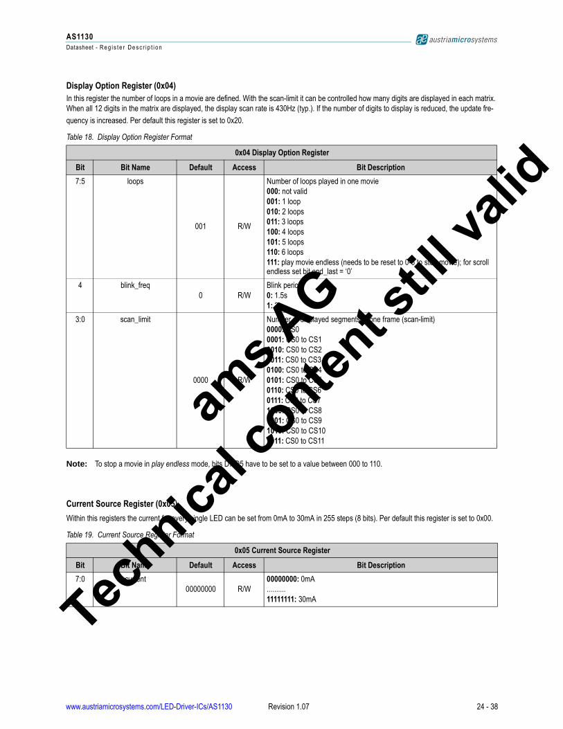
Display Option Register (0x04)
In this register the number of loops in a movie are defined. With the scan-limit it can be controlled how many digits are displayed in each matrix.
When all 12 digits in the matrix are displayed, the display scan rate is 430Hz (typ.). If the number of digits to display is reduced, the update fre-
quency is increased. Per default this register is set to 0x20.
Note: To stop a movie in play endless mode, bits D7:D5 have to be set to a value between 000 to 110.
Current Source Register (0x05)
Within this registers the current for every single LED can be set from 0mA to 30mA in 255 steps (8 bits). Per default this register is set to 0x00.
Table 18. Display Option Register Format
0x04 Display Option Register
Bit Bit Name Default Access Bit Description
7:5 loops
001 R/W
Number of loops played in one movie
000: not valid
001: 1 loop
010: 2 loops
011: 3 loops
100: 4 loops
101: 5 loops
110: 6 loops
111: play movie endless (needs to be reset to 0-6 to stop movie); for scroll endless set bit end_last = ‘0’
4 blink_freq
0 R/W
Blink period
0: 1.5s
1: 3s
3:0 scan_limit
0000 R/W
Number of displayed segments in one frame (scan-limit)
0000: CS0
0001: CS0 to CS1
0010: CS0 to CS2
0011: CS0 to CS3
0100: CS0 to CS4
0101: CS0 to CS5
0110: CS0 to CS6
0111: CS0 to CS7
1000: CS0 to CS8
1001: CS0 to CS9
1010: CS0 to CS10
1011: CS0 to CS11
Table 19. Current Source Register Format
0x05 Current Source Register
Bit Bit Name Default Access Bit Description
7:0 current
00000000 R/W
00000000: 0mA
..........
11111111: 30mA
ams A
G
Technica
l conten
t still
va
www.austriamicrosystems.com/LED-Driver-ICs/AS1130 Revision 1.07 24 - 38
AS1130
Datasheet - R e g i s t e r D e s c r i p t i on
lid
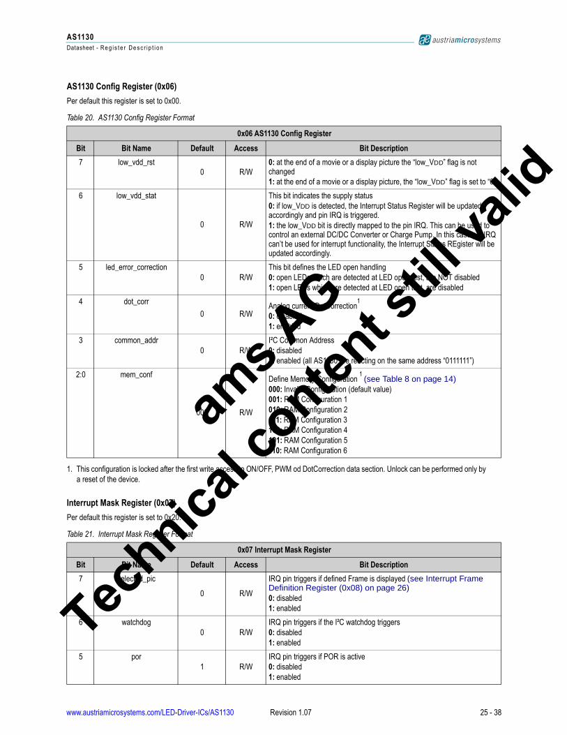
AS1130 Config Register (0x06)
Per default this register is set to 0x00.
Interrupt Mask Register (0x07)
Per default this register is set to 0x20.
Table 20. AS1130 Config Register Format
0x06 AS1130 Config Register
Bit Bit Name Default Access Bit Description
7 low_vdd_rst0 R/W
0: at the end of a movie or a display picture the “low_VDD” flag is not changed
1: at the end of a movie or a display picture, the “low_VDD” flag is set to “0”
6 low_vdd_stat
0 R/W
This bit indicates the supply status
0: if low_VDD is detected, the Interrupt Status Register will be updated accordingly and pin IRQ is triggered.
1: the low_VDD bit is directly mapped to the pin IRQ. This can be used to control an external DC/DC Converter or Charge Pump. In this case pin IRQ can’t be used for interrupt functionality, the Interrupt Status REgister will be updated accordingly.
5 led_error_correction
0 R/W
This bit defines the LED open handling
0: open LEDs which are detected at LED open test, are NOT disabled
1: open LEDs which are detected at LED open test, are disabled
4 dot_corr
0 R/WAnalog current DotCorrection
1
0: disabled
1: enabled
1. This configuration is locked after the first write access to ON/OFF, PWM od DotCorrection data section. Unlock can be performed only by
a reset of the device.
3 common_addr
0 R/W
I²C Common Address
0: disabled
1: enabled (all AS1130 are reacting on the same address “0111111”)
2:0 mem_conf
000 R/W
Define Memory Configuration 1 (see Table 8 on page 14)
000: Invalid Configuration (default value)
001: RAM Configuration 1
010: RAM Configuration 2
011: RAM Configuration 3
100: RAM Configuration 4
101: RAM Configuration 5
110: RAM Configuration 6
Table 21. Interrupt Mask Register Format
0x07 Interrupt Mask Register
Bit Bit Name Default Access Bit Description
7 selected_pic
0 R/W
IRQ pin triggers if defined Frame is displayed (see Interrupt Frame Definition Register (0x08) on page 26)0: disabled
1: enabled
6 watchdog
0 R/W
IRQ pin triggers if the I²C watchdog triggers
0: disabled
1: enabled
5 por
1 R/W
IRQ pin triggers if POR is active
0: disabled
1: enabled
ams A
G
Technica
l conten
t still
va
www.austriamicrosystems.com/LED-Driver-ICs/AS1130 Revision 1.07 25 - 38
AS1130
Datasheet - R e g i s t e r D e s c r i p t i on
lid
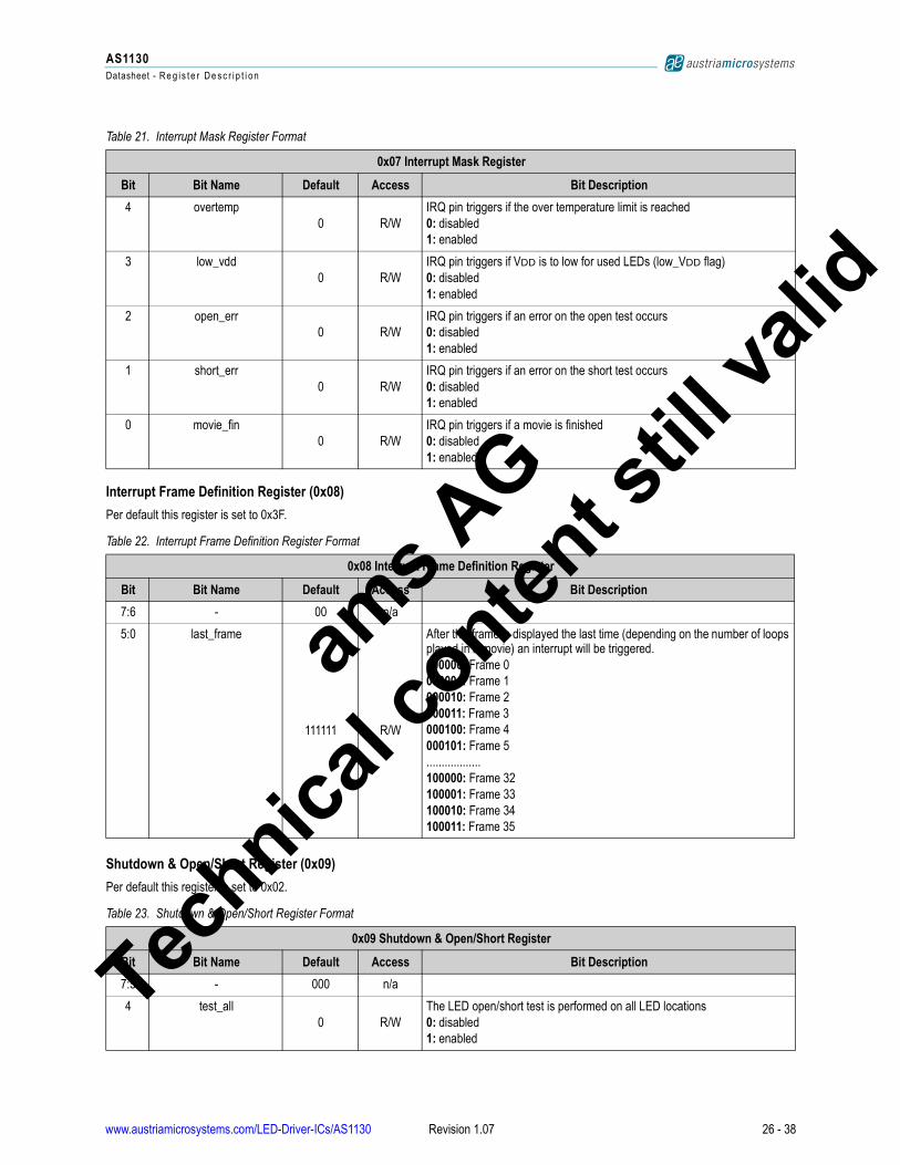
Interrupt Frame Definition Register (0x08)
Per default this register is set to 0x3F.
Shutdown & Open/Short Register (0x09)
Per default this register is set to 0x02.
4 overtemp
0 R/W
IRQ pin triggers if the over temperature limit is reached
0: disabled
1: enabled
3 low_vdd
0 R/W
IRQ pin triggers if VDD is to low for used LEDs (low_VDD flag)
0: disabled
1: enabled
2 open_err
0 R/W
IRQ pin triggers if an error on the open test occurs
0: disabled
1: enabled
1 short_err
0 R/W
IRQ pin triggers if an error on the short test occurs
0: disabled
1: enabled
0 movie_fin
0 R/W
IRQ pin triggers if a movie is finished
0: disabled
1: enabled
Table 22. Interrupt Frame Definition Register Format
0x08 Interrupt Frame Definition Register
Bit Bit Name Default Access Bit Description
7:6 - 00 n/a
5:0 last_frame
111111 R/W
After this frame is displayed the last time (depending on the number of loops played in a movie) an interrupt will be triggered.
000000: Frame 0
000001: Frame 1
000010: Frame 2
000011: Frame 3
000100: Frame 4
000101: Frame 5
..................
100000: Frame 32
100001: Frame 33
100010: Frame 34
100011: Frame 35
Table 23. Shutdown & Open/Short Register Format
0x09 Shutdown & Open/Short Register
Bit Bit Name Default Access Bit Description
7:5 - 000 n/a
4 test_all
0 R/W
The LED open/short test is performed on all LED locations
0: disabled
1: enabled
Table 21. Interrupt Mask Register Format
0x07 Interrupt Mask Register
Bit Bit Name Default Access Bit Description
ams A
G
Technica
l conten
t still
va
www.austriamicrosystems.com/LED-Driver-ICs/AS1130 Revision 1.07 26 - 38
AS1130
Datasheet - R e g i s t e r D e s c r i p t i on
lid
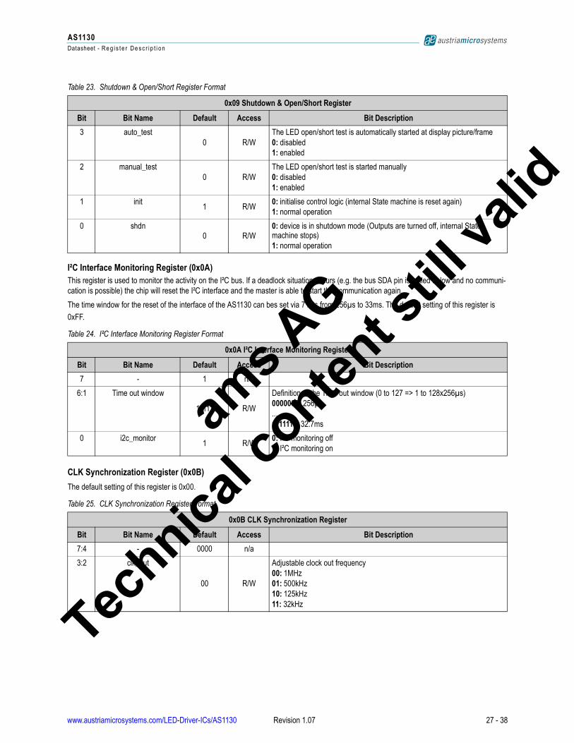
I²C Interface Monitoring Register (0x0A)This register is used to monitor the activity on the I²C bus. If a deadlock situation occurs (e.g. the bus SDA pin is pulled to low and no communi-
cation is possible) the chip will reset the I²C interface and the master is able to start the communication again.
The time window for the reset of the interface of the AS1130 can bes set via 7 bits from 256µs to 33ms. The default setting of this register is
0xFF.
CLK Synchronization Register (0x0B)
The default setting of this register is 0x00.
3 auto_test
0 R/W
The LED open/short test is automatically started at display picture/frame
0: disabled
1: enabled
2 manual_test
0 R/W
The LED open/short test is started manually
0: disabled
1: enabled
1 init1 R/W
0: initialise control logic (internal State machine is reset again)
1: normal operation
0 shdn0 R/W
0: device is in shutdown mode (Outputs are turned off, internal State machine stops)
1: normal operation
Table 24. I²C Interface Monitoring Register Format
0x0A I²C Interface Monitoring Register
Bit Bit Name Default Access Bit Description
7 - 1 n/a
6:1 Time out window
11111 R/W
Definition of the Time out window (0 to 127 => 1 to 128x256µs)
0000000: 256µs
........
1111111: 32.7ms
0 i2c_monitor1 R/W
0: I²C monitoring off
1: I²C monitoring on
Table 25. CLK Synchronization Register Format
0x0B CLK Synchronization Register
Bit Bit Name Default Access Bit Description
7:4 - 0000 n/a
3:2 clk_out
00 R/W
Adjustable clock out frequency
00: 1MHz
01: 500kHz
10: 125kHz
11: 32kHz
Table 23. Shutdown & Open/Short Register Format
0x09 Shutdown & Open/Short Register
Bit Bit Name Default Access Bit Description
ams A
G
Technica
l conten
t still
va
www.austriamicrosystems.com/LED-Driver-ICs/AS1130 Revision 1.07 27 - 38
AS1130
Datasheet - R e g i s t e r D e s c r i p t i on
lid
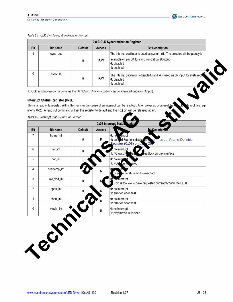
Interrupt Status Register (0x0E)This is a read only register. Within this register the cause of an interrupt can be read out. After power up or a reset the default setting of this reg-
ister is 0x20. A read out command will set this register to default and the IRQ pin will be released again.
1 sync_out
0 R/W
The internal oscillator is used as system-clk. The selected clk frequency is
available on pin D4 for synchronization. (Output)1
0: disabled
1: enabled
0 sync_in
0 R/WThe internal oscillator is disabled. Pin D4 is used as clk input for system-clk.
1
0: disabled
1: enabled
1. CLK synchronization is done via the SYNC pin. Only one option can be activated (Input or Output).
Table 26. Interrupt Status Register Format
0x0E Interrupt Status Register
Bit Bit Name Default Access Bit Description
7 frame_int0 R
0: no interrupt
1: defined Frame is displayed (see Interrupt Frame Definition Register (0x08) on page 26)
6 i2c_int0 R
0: no interrupt
1: I²C watchdog reports a deadlock on the interface
5 por_int1 R
0: no interrupt
1: POR was triggered
4 overtemp_int0 R
0: no interrupt
1: over temperature limit is reached
3 low_vdd_int0 R
0: no interrupt
1: VDD is too low to drive requested current through the LEDs
2 open_int0 R
0: no interrupt
1: error on open test
1 short_int0 R
0: no interrupt
1: error on short test
0 movie_int0 R
0: no interrupt
1: play movie is finished
Table 25. CLK Synchronization Register Format
0x0B CLK Synchronization Register
Bit Bit Name Default Access Bit Description
ams A
G
Technica
l conten
t still
va
www.austriamicrosystems.com/LED-Driver-ICs/AS1130 Revision 1.07 28 - 38
AS1130
Datasheet - R e g i s t e r D e s c r i p t i on
lid
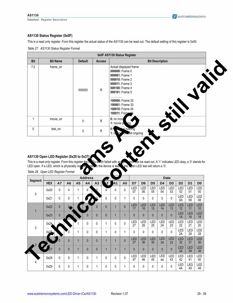
AS1130 Status Register (0x0F)
This is a read only register. From this register the actual status of the AS1130 can be read out. The default setting of this register is 0x00.
AS1130 Open LED Register (0x20 to 0x37)
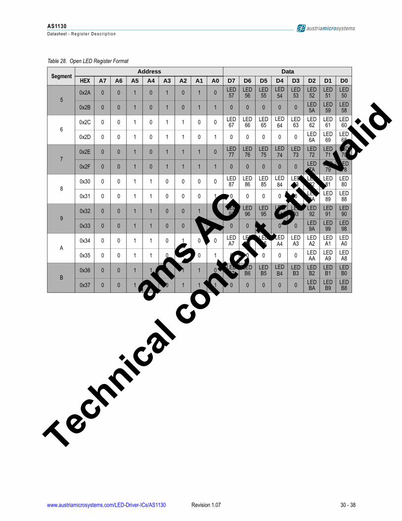
This is a read only register. From this register the LED’s which failed with an open error can be read out. A ‘1’ indicates LED okay, a ‘0’ stands for
LED open. If a LED, which is physically not connected to the device is tested, the Open LED test will return a ‘0’.
Table 27. AS1130 Status Register Format
0x0F AS1130 Status Register
Bit Bit Name Default Access Bit Description
7:2 frame_on
000000 R
Actual displayed frame
000000: Frame 0
000001: Frame 1
000010: Frame 2
000011: Frame 3
000100: Frame 4
000101: Frame 5
...............
100000: Frame 32
100001: Frame 33
100010: Frame 34
100011: Frame 35
1 movie_on0 R
0: no movie
1: movie playing
0 test_on0 R
0: no test is running
1: open/short test ongoing
Table 28. Open LED Register Format
SegmentAddress Data
HEX A7 A6 A5 A4 A3 A2 A1 A0 D7 D6 D5 D4 D3 D2 D1 D0
0
0x20 0 0 1 0 0 0 0 0LED 07
LED 06
LED 05
LED 04
LED 03
LED 02
LED 01
LED 00
0x21 0 0 1 0 0 0 0 1 0 0 0 0 0LED 0A
LED 09
LED 08
1
0x22 0 0 1 0 0 0 1 0LED 17
LED 16
LED 15
LED 14
LED 13
LED 12
LED 11
LED 10
0x23 0 0 1 0 0 0 1 1 0 0 0 0 0LED 1A
LED 19
LED 18
2
0x24 0 0 1 0 0 1 0 0LED 27
LED 26
LED 25
LED 24
LED 23
LED 22
LED 21
LED 20
0x25 0 0 1 0 0 1 0 1 0 0 0 0 0LED 2A
LED 29
LED 28
3
0x26 0 0 1 0 0 1 1 0LED 37
LED 36
LED 35
LED34
LED33
LED 32
LED 31
LED 30
0x27 0 0 1 0 0 1 1 1 0 0 0 0 0LED 3A
LED 39
LED 38
4
0x28 0 0 1 0 1 0 0 0LED 47
LED 46
LED 45
LED44
LED 43
LED 42
LED 41
LED 40
0x29 0 0 1 0 1 0 0 1 0 0 0 0 0LED 4A
LED 49
LED 48
ams A
G
Technica
l conten
t still
va
www.austriamicrosystems.com/LED-Driver-ICs/AS1130 Revision 1.07 29 - 38
AS1130
Datasheet - R e g i s t e r D e s c r i p t i on
lid
50x2A 0 0 1 0 1 0 1 0LED 57
LED 56
LED 55
LED54
LED 53
LED 52
LED 51
LED 50
0x2B 0 0 1 0 1 0 1 1 0 0 0 0 0LED 5A
LED 59
LED 58
6
0x2C 0 0 1 0 1 1 0 0LED 67
LED 66
LED 65
LED64
LED 63
LED 62
LED 61
LED 60
0x2D 0 0 1 0 1 1 0 1 0 0 0 0 0LED 6A
LED 69
LED 68
7
0x2E 0 0 1 0 1 1 1 0LED 77
LED 76
LED 75
LED74
LED 73
LED 72
LED 71
LED 70
0x2F 0 0 1 0 1 1 1 1 0 0 0 0 0LED 7A
LED 79
LED 78
8
0x30 0 0 1 1 0 0 0 0LED 87
LED 86
LED 85
LED84
LED 83
LED 82
LED 81
LED 80
0x31 0 0 1 1 0 0 0 1 0 0 0 0 0LED 8A
LED 89
LED 88
9
0x32 0 0 1 1 0 0 1 0LED 97
LED 96
LED 95
LED94
LED 93
LED 92
LED 91
LED 90
0x33 0 0 1 1 0 0 1 1 0 0 0 0 0LED 9A
LED 99
LED 98
A
0x34 0 0 1 1 0 1 0 0LED A7
LED A6
LED A5
LEDA4
LED A3
LED A2
LED A1
LED A0
0x35 0 0 1 1 0 1 0 1 0 0 0 0 0LED AA
LED A9
LED A8
B
0x36 0 0 1 1 0 1 1 0LED B7
LED B6
LED B5
LEDB4
LED B3
LED B2
LED B1
LED B0
0x37 0 0 1 1 0 1 1 1 0 0 0 0 0LED BA
LED B9
LED B8
Table 28. Open LED Register Format
SegmentAddress Data
HEX A7 A6 A5 A4 A3 A2 A1 A0 D7 D6 D5 D4 D3 D2 D1 D0
ams A
G
Technica
l conten
t still
va
www.austriamicrosystems.com/LED-Driver-ICs/AS1130 Revision 1.07 30 - 38

AS1130
Datasheet - Ty p i ca l A pp l i c a t i o n
lid
10 Typical Application
Scroll FunctionThe AS1130 offers a feature for scrolling a picture through the matrix without the need of communication via a µP. The scrolling can be done in
the whole matrix (11x12) or optimized for a ticker in a 5x24 Matrix (see Figure 25).
Figure 25. LED configuration for 5LED block scroll function
In the movie display mode the frame is shown in the matrix at once. On the contrary in the scroll function the frame is shifted through the matrix
segment after segment (CS0 to CS1 to CS2 to CS3 ......).
Figure 26. Scrolling
ams A
G
Technica
l conten
t still
va
www.austriamicrosystems.com/LED-Driver-ICs/AS1130 Revision 1.07 31 - 38

AS1130
Datasheet - Ty p i ca l A pp l i c a t i o n
lid
Figure 27. Ticker Application with 5x96 LED Matrix
ams A
G
Technica
l conten
t still
va
www.austriamicrosystems.com/LED-Driver-ICs/AS1130 Revision 1.07 32 - 38

AS1130
Datasheet - Ty p i ca l A pp l i c a t i o n
lid
LED Current CalculationThe current through a LED in the matrix is set via three registers (Current Source Register, Dot Correction and PWM). The resulting current
through the single LED can be calculated as shown in the following.
First it’s necessary to calculate the time how long one LED will be ON.
Where:
tLEDon . . . . time where the LED is ON
PWM . . . value set in the register (0 - 256), (see Table 11 on page 18)
fOSC . . . frequency set in the CLK Synchronization Register, (see Table 25 on page 27)
The refresh rate is defined by the scan-limit and fOSC.
Where:
tREFRESH . . . time needed to refresh the matrix
scan-limit . . . is set via the Display Option Register (0 - 11), (see Table 18 on page 24)
fOSC . . . frequency set in the CLK Synchronization Register, (see Table 25 on page 27)
With the LED on-time and the refresh rate an average LED ON factor can be calculated.
The resulting current is then the Segment Current (set in the Current Source Register) times the average LED ON factor.
Where:
ISEG . . . Segment Current set via register (see Table 19 on page 24)
Example:
Assume that following conditions are set in the registers: PWM = 256, scan-limit = 5 (half filled matrix, 66 LEDs), ISEG = 30mA
(EQ 1)tLEDonPWMfOSC--------------=
(EQ 2)tREFRESHscanlimit 1+( ) 256×
fOSC------------------------------------------------------=
(EQ 3)LEDonavg
tLEDon
tREFRESH------------------------ PWM
scanlimit 1+( ) 256×------------------------------------------------------= =
(EQ 4)ILEDavg ISEG LEDonavg× ISEGPWM
scanlimit 1+( ) 256×------------------------------------------------------×= =
(EQ 5)ILEDavg 30mA256
5 1+( ) 256×--------------------------------× 5mA= =
ams A
G
Technica
l conten
t still
va
www.austriamicrosystems.com/LED-Driver-ICs/AS1130 Revision 1.07 33 - 38
AS1130
Datasheet - P ac k a ge D ra w i n gs a nd M a r k i n gs
lid
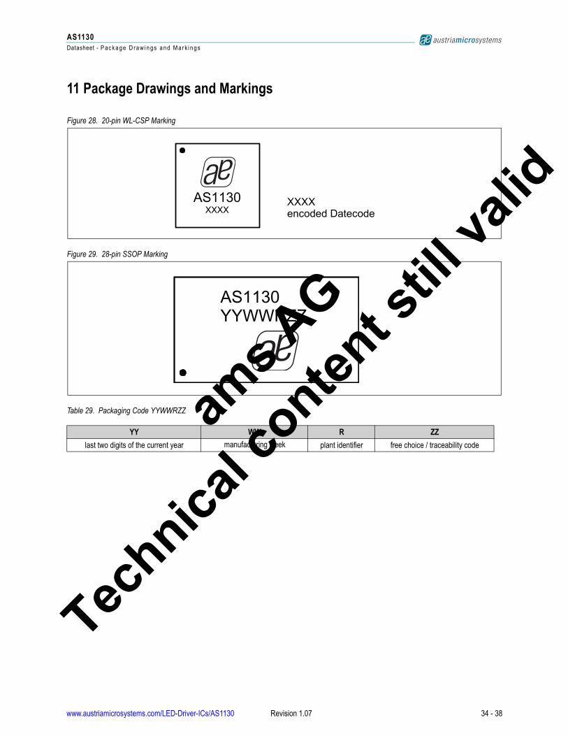
11 Package Drawings and Markings
Figure 28. 20-pin WL-CSP Marking
Figure 29. 28-pin SSOP Marking
Table 29. Packaging Code YYWWRZZ
YY WW R ZZ
last two digits of the current year manufacturing week plant identifier free choice / traceability code
ams A
G
Technica
l conten
t still
va
www.austriamicrosystems.com/LED-Driver-ICs/AS1130 Revision 1.07 34 - 38
AS1130
Datasheet - P ac k a ge D ra w i n gs a nd M a r k i n gs
lid
www.austriamicrosystems.com/LED-Driver-ICs/AS1130 Revision 1.07 35 - 38
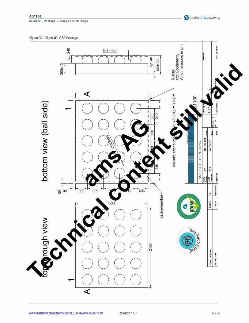
Figure 30. 20-pin WL-CSP Package
ams A
G
Technica
l conten
t still
va
AS1130
Datasheet - P ac k a ge D ra w i n gs a nd M a r k i n gs
lid
www.austriamicrosystems.com/LED-Driver-ICs/AS1130 Revision 1.07 36 - 38
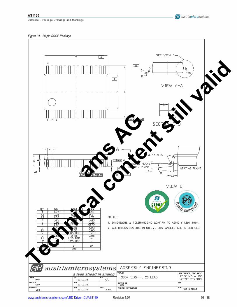
Figure 31. 28-pin SSOP Package
ams A
G
Technica
l conten
t still
va
AS1130
Datasheet - O r d e r i ng I n f o r ma t i on
lid
12 Ordering Information
The devices are available as the standard products shown in Table 30.
*) on request
Note: All products are RoHS compliant and austriamicrosystems green.
Buy our products or get free samples online at ICdirect: http://www.austriamicrosystems.com/ICdirect
Technical Support is found at http://www.austriamicrosystems.com/Technical-Support
For further information and requests, please contact us mailto:[email protected]
or find your local distributor at http://www.austriamicrosystems.com/distributor
Table 30. Ordering Information
Ordering Code Marking Logic Levels Address Description Delivery Form Package
AS1130-BSST AS1130 CMOS
0x30 - 0x37
132-LED Cross-Plexing Driver with scrolling Function
Tape and Reel
28-pin SSOPAS1130B-BSST* AS1130B Mobile
132-LED Cross-Plexing Driver with scrolling Function
Tape and Reel
AS1130C-BSST* AS1130C CMOS
0x38 - 0x3E
132-LED Cross-Plexing Driver with scrolling Function
Tape and Reel
AS1130D-BSST* AS1130D Mobile132-LED Cross-Plexing Driver with
scrolling FunctionTape and Reel
AS1130-BWLT AS1130 CMOS
0x30 - 0x37
132-LED Cross-Plexing Driver with scrolling Function
Tape and Reel
20-pin WL-CSPAS1130B-BWLT* AS1130B Mobile
132-LED Cross-Plexing Driver with scrolling Function
Tape and Reel
AS1130C-BWLT* tbd CMOS
0x38 - 0x3E
132-LED Cross-Plexing Driver with scrolling Function
Tape and Reel
AS1130D-BWLT* tbd Mobile132-LED Cross-Plexing Driver with
scrolling FunctionTape and Reel
ams A
G
Technica
l conten
t still
va
www.austriamicrosystems.com/LED-Driver-ICs/AS1130 Revision 1.07 37 - 38

AS1130
Datasheet
lid
Copyrights
Copyright © 1997-2012, austriamicrosystems AG, Tobelbaderstrasse 30, 8141 Unterpremstaetten, Austria-Europe. Trademarks Registered ®.
All rights reserved. The material herein may not be reproduced, adapted, merged, translated, stored, or used without the prior written consent of
the copyright owner.
All products and companies mentioned are trademarks or registered trademarks of their respective companies.
Disclaimer
Devices sold by austriamicrosystems AG are covered by the warranty and patent indemnification provisions appearing in its Term of Sale. aus-
triamicrosystems AG makes no warranty, express, statutory, implied, or by description regarding the information set forth herein or regarding the
freedom of the described devices from patent infringement. austriamicrosystems AG reserves the right to change specifications and prices at
any time and without notice. Therefore, prior to designing this product into a system, it is necessary to check with austriamicrosystems AG for
current information. This product is intended for use in normal commercial applications. Applications requiring extended temperature range,
unusual environmental requirements, or high reliability applications, such as military, medical life-support or life-sustaining equipment are specif-
ically not recommended without additional processing by austriamicrosystems AG for each application. For shipments of less than 100 parts the
manufacturing flow might show deviations from the standard production flow, such as test flow or test location.
The information furnished here by austriamicrosystems AG is believed to be correct and accurate. However, austriamicrosystems AG shall not
be liable to recipient or any third party for any damages, including but not limited to personal injury, property damage, loss of profits, loss of use,
interruption of business or indirect, special, incidental or consequential damages, of any kind, in connection with or arising out of the furnishing,
performance or use of the technical data herein. No obligation or liability to recipient or any third party shall arise or flow out of
austriamicrosystems AG rendering of technical or other services.
Contact Information
Headquarters
austriamicrosystems AG
Tobelbaderstrasse 30
A-8141 Unterpremstaetten, Austria
Tel: +43 (0) 3136 500 0
Fax: +43 (0) 3136 525 01
For Sales Offices, Distributors and Representatives, please visit:
http://www.austriamicrosystems.com/contact
ams A
G
Technica
l conten
t still
va
www.austriamicrosystems.com/LED-Driver-ICs/AS1130 Revision 1.07 38 - 38