Embed Size (px)
Citation preview
Document Feedback AS3418 Content Guide
Datasheet • PUBLIC DS000507 • v4-00 • 2020-Jan-23 77 2
Content Guide
1 General Description ....................... 3
1.1 Key Benefits & Features .............................. 3 1.2 Applications .................................................. 4 1.3 Block Diagram .............................................. 4
2 Ordering Information ..................... 5
3 Pin Assignment ............................. 6
3.1 Pin Diagram .................................................. 6 3.2 Pin Description ............................................. 6
4 Absolute Maximum Ratings .......... 9
5 Electrical Characteristics ............ 10
6 Functional Description ................ 12
6.1 Audio Line Input ......................................... 12 6.2 Microphone Inputs ...................................... 13 6.3 Microphone Supply .................................... 19 6.4 Headphone Amplifier .................................. 21 6.5 Music Bypass Switch ................................. 25 6.6 Operational Amplifier .................................. 28 6.7 System ....................................................... 30
6.8 Operation Modes ....................................... 33 6.9 VNEG Charge Pump .................................... 38 6.10 EEPROM .................................................... 39 6.11 Production Trimming Interface ................... 41 6.12 I2C Interface ............................................... 42
7 Register Description ................... 47
7.1 Register Overview ...................................... 47 7.2 Detailed Register Description .................... 49
8 Application Information .............. 70
8.1 Schematic .................................................. 70 8.2 External Components ................................ 72
9 Package Drawings & Markings ... 74
10 Revision Information ................... 76
11 Legal Information ........................ 77
Document Feedback AS3418 General Description
Datasheet • PUBLIC DS000507 • v4-00 • 2020-Jan-23 77 3
1 General Description
The AS3418 speaker driver with Ambient Noise Cancelling function for headsets, headphones or ear
pieces. They are intended to improve quality of e.g. music listening, a phone conversation etc. by
reducing background ambient noise.
The fully analog implementation allows the lowest power consumption, lowest system BOM cost and
most natural received voice enhancement otherwise difficult to achieve with DSP implementations.
The device is designed to be easily applied to existing architectures.
An internal EEPROM can be optionally used to store the microphones gain calibration settings. The
AS3418 can be used in different configurations for best trade-off of noise cancellation, required
filtering functions and mechanical designs.
The AS3418 targeting feed-forward topology is used to effectively reduce frequencies typically up to 2-
3 kHz. The typical bandwidth for a feed-forward system is from 20Hz up to 3 kHz which is lower than
the feed-forward systems.
The filter loop for the system is determined by measurements, for each specific headset individually,
and depends very much on mechanical designs. The gain and phase compensation filter network is
implemented with cheap resistors and capacitors for lowest system costs.
1.1 Key Benefits & Features
The benefits and features of AS3418, Low Noise ANC Solution, are listed below:
Figure 1:
Added Value of Using AS3418
Benefits Features
Low Noise Floor Low Noise Amplifiers
Integrated Music Bypass Switch Depletion mode transistors for passive music bypass
Smallest ANC form factor WL-CSP package 2.645mm x 2.545mm; 0.4mm pitch
Reprogrammable ANC settings EEPROM Memory for system settings
Document Feedback AS3418 General Description
Datasheet • PUBLIC DS000507 • v4-00 • 2020-Jan-23 77 4
1.2 Applications
Ear Pieces
Headsets
Hands-Free Kits
Mobile Phones
Voice Communicating Devices
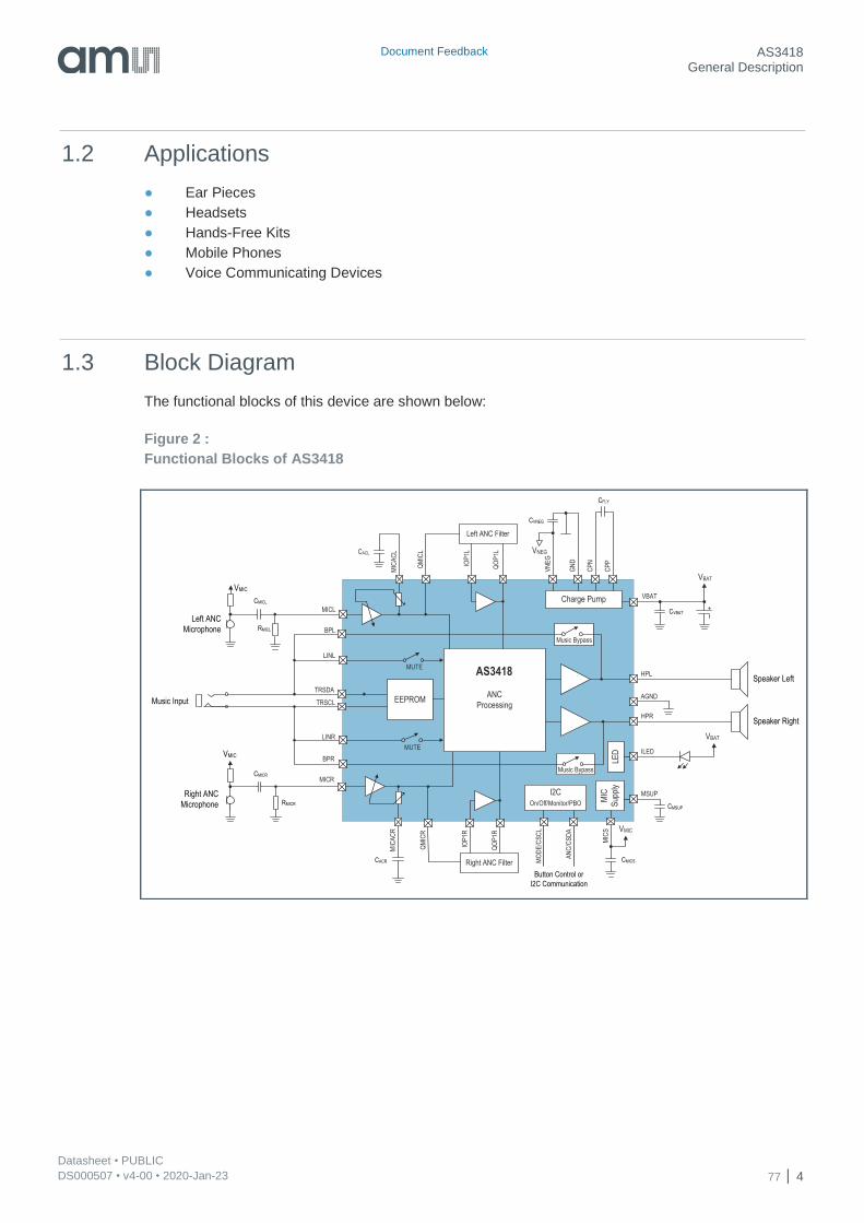
1.3 Block Diagram
The functional blocks of this device are shown below:
Figure 2 :
Functional Blocks of AS3418
VBATC
PN
CP
P
GN
D
VN
EG
Charge PumpM
ICS
MICL
VMIC
VMIC
VMIC
VNEG
I2C
On/Off/Monitor/PBO
VBAT
LINL
LINR
MICR
Left ANC Filter
Right ANC Filter
QM
ICR
IOP
1R
QO
P1R
QM
ICL
IOP
1L
QO
P1L
HPL
HPR
AGND
AN
C/C
SD
A
MO
DE
/CS
CL
ANC
Processing
MIC
Sup
ply
TRSCL
Music Bypass
Music Bypass
MUTE
MUTE
CVBAT
CFLY
CVNEG
CMICL
CMICR
AS3418
TRSDA
CACR
CACL
MIC
AC
LM
ICA
CR
EEPROM
RMICL
RMICRCMSUP
MSUP
CMICS
BPR
BPL
ILED
LED
VBAT
Speaker Left
Speaker Right
Right ANC
Microphone
Left ANC
Microphone
Music Input
Button Control or
I2C Communication
Document Feedback AS3418 Ordering Information
Datasheet • PUBLIC DS000507 • v4-00 • 2020-Jan-23 77 5
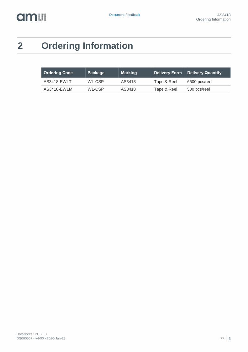
2 Ordering Information
Ordering Code Package Marking Delivery Form Delivery Quantity
AS3418-EWLT WL-CSP AS3418 Tape & Reel 6500 pcs/reel
AS3418-EWLM WL-CSP AS3418 Tape & Reel 500 pcs/reel
Document Feedback AS3418 Pin Assignment
Datasheet • PUBLIC DS000507 • v4-00 • 2020-Jan-23 77 6
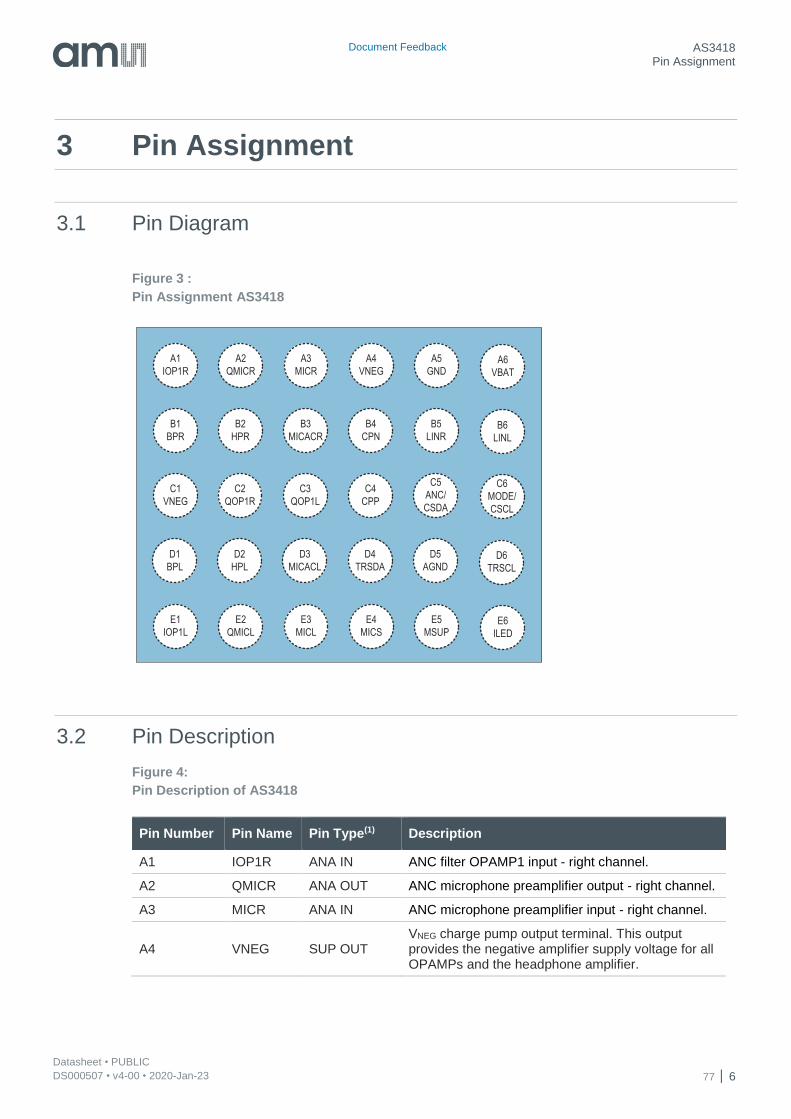
3 Pin Assignment
3.1 Pin Diagram
Figure 3 :
Pin Assignment AS3418
3.2 Pin Description
Figure 4:
Pin Description of AS3418
Pin Number Pin Name Pin Type(1) Description
A1 IOP1R ANA IN ANC filter OPAMP1 input - right channel.
A2 QMICR ANA OUT ANC microphone preamplifier output - right channel.
A3 MICR ANA IN ANC microphone preamplifier input - right channel.
A4 VNEG SUP OUT VNEG charge pump output terminal. This output provides the negative amplifier supply voltage for all OPAMPs and the headphone amplifier.
A2
QMICR
A3
MICR
A4
VNEG
A5
GND
B2
HPR
B3
MICACR
B4
CPN
B5
LINR
C2
QOP1R
C3
QOP1L
C4
CPP
C5
ANC/
CSDA
D2
HPL
D3
MICACL
D4
TRSDA
D5
AGND
A6
VBAT
B6
LINL
C6
MODE/
CSCL
D6
TRSCL
E2
QMICL
E3
MICL
E4
MICS
E5
MSUPE6
ILED
A1
IOP1R
B1
BPR
C1
VNEG
D1
BPL
E1
IOP1L
Document Feedback AS3418 Pin Assignment
Datasheet • PUBLIC DS000507 • v4-00 • 2020-Jan-23 77 7
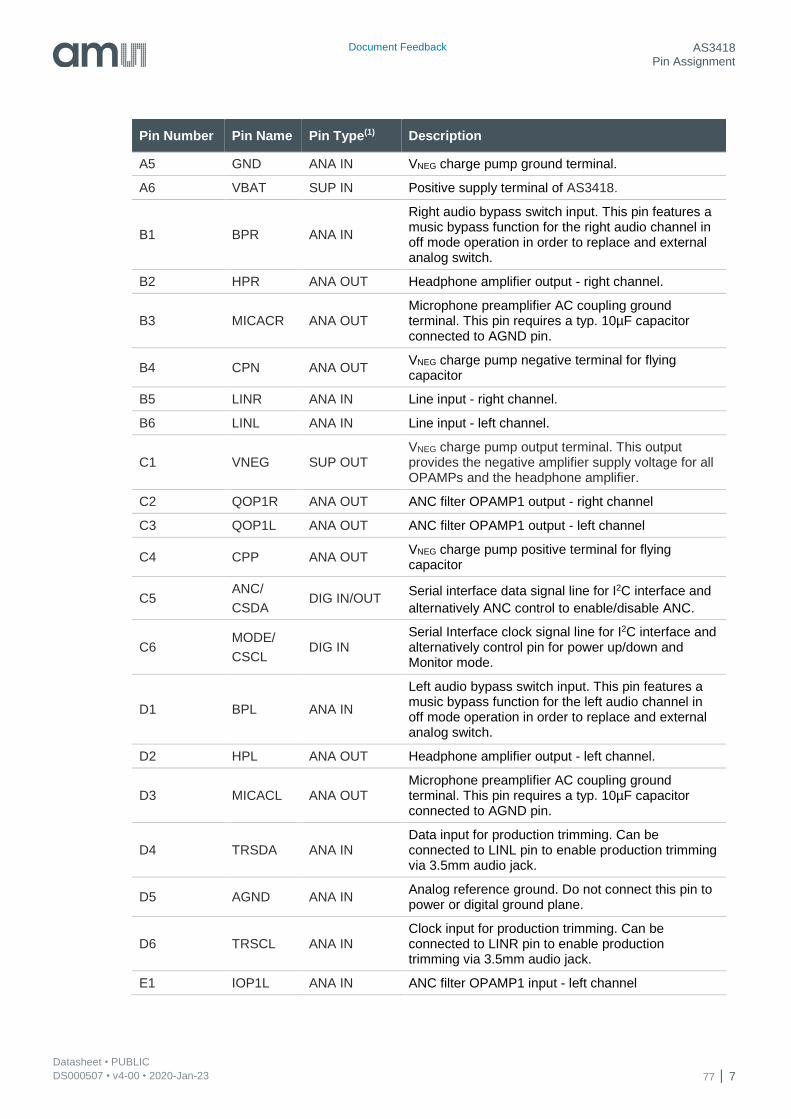
Pin Number Pin Name Pin Type(1) Description
A5 GND ANA IN VNEG charge pump ground terminal.
A6 VBAT SUP IN Positive supply terminal of AS3418.
B1 BPR ANA IN
Right audio bypass switch input. This pin features a music bypass function for the right audio channel in off mode operation in order to replace and external analog switch.
B2 HPR ANA OUT Headphone amplifier output - right channel.
B3 MICACR ANA OUT Microphone preamplifier AC coupling ground terminal. This pin requires a typ. 10µF capacitor connected to AGND pin.
B4 CPN ANA OUT VNEG charge pump negative terminal for flying capacitor
B5 LINR ANA IN Line input - right channel.
B6 LINL ANA IN Line input - left channel.
C1 VNEG SUP OUT VNEG charge pump output terminal. This output provides the negative amplifier supply voltage for all OPAMPs and the headphone amplifier.
C2 QOP1R ANA OUT ANC filter OPAMP1 output - right channel
C3 QOP1L ANA OUT ANC filter OPAMP1 output - left channel
C4 CPP ANA OUT VNEG charge pump positive terminal for flying capacitor
C5 ANC/
CSDA DIG IN/OUT
Serial interface data signal line for I2C interface and
alternatively ANC control to enable/disable ANC.
C6 MODE/
CSCL DIG IN
Serial Interface clock signal line for I2C interface and alternatively control pin for power up/down and Monitor mode.
D1 BPL ANA IN
Left audio bypass switch input. This pin features a music bypass function for the left audio channel in off mode operation in order to replace and external analog switch.
D2 HPL ANA OUT Headphone amplifier output - left channel.
D3 MICACL ANA OUT Microphone preamplifier AC coupling ground terminal. This pin requires a typ. 10µF capacitor connected to AGND pin.
D4 TRSDA ANA IN Data input for production trimming. Can be connected to LINL pin to enable production trimming via 3.5mm audio jack.
D5 AGND ANA IN Analog reference ground. Do not connect this pin to power or digital ground plane.
D6 TRSCL ANA IN Clock input for production trimming. Can be connected to LINR pin to enable production trimming via 3.5mm audio jack.
E1 IOP1L ANA IN ANC filter OPAMP1 input - left channel
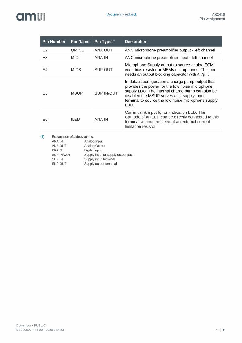
Document Feedback AS3418 Pin Assignment
Datasheet • PUBLIC DS000507 • v4-00 • 2020-Jan-23 77 8
Pin Number Pin Name Pin Type(1) Description
E2 QMICL ANA OUT ANC microphone preamplifier output - left channel
E3 MICL ANA IN ANC microphone preamplifier input - left channel
E4 MICS SUP OUT Microphone Supply output to source analog ECM via a bias resistor or MEMs microphones. This pin needs an output blocking capacitor with 4.7µF.
E5 MSUP SUP IN/OUT
In default configuration a charge pump output that provides the power for the low noise microphone supply LDO. The internal charge pump can also be disabled the MSUP serves as a supply input terminal to source the low noise microphone supply LDO.
E6 ILED ANA IN
Current sink input for on-indication LED. The Cathode of an LED can be directly connected to this terminal without the need of an external current limitation resistor.
(1) Explanation of abbreviations:
ANA IN Analog Input
ANA OUT Analog Output
DIG IN Digital Input
SUP IN/OUT Supply input or supply output pad
SUP IN Supply input terminal
SUP OUT Supply output terminal
Document Feedback AS3418 Absolute Maximum Ratings
Datasheet • PUBLIC DS000507 • v4-00 • 2020-Jan-23 77 9
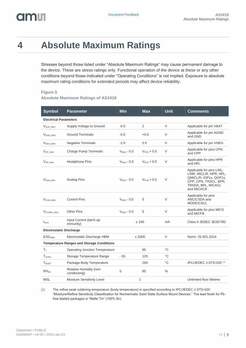
4 Absolute Maximum Ratings
Stresses beyond those listed under “Absolute Maximum Ratings“ may cause permanent damage to
the device. These are stress ratings only. Functional operation of the device at these or any other
conditions beyond those indicated under “Operating Conditions” is not implied. Exposure to absolute
maximum rating conditions for extended periods may affect device reliability.
Figure 5
Absolute Maximum Ratings of AS3418
Symbol Parameter Min Max Unit Comments
Electrical Parameters
VSUP_MAX Supply Voltage to Ground -0.5 2 V Applicable for pin VBAT
VGND_MAX Ground Terminals -0.5 +0.5 V Applicable for pin AGND and GND
VNEG_MAX Negative Terminals -2.0 0.5 V Applicable for pin VNEG
VCP_MAX Charge Pump Terminals VNEG - 0.5 VPOS + 0.5 V Applicable for pins CPN and CPP
VHP_MAX Headphone Pins VNEG - 0.5 VPOS + 0.5 V Applicable for pins HPR and HPL
VANA_MAX Analog Pins VNEG - 0.5 VPOS + 0.5 V
Applicable for pins LINL, LINR, MICL/R, HPR, HPL, QMICL/R, IOP1x, QOP1x, CPP, CPN, TRSCL, BPR, TRSDA, BPL, MICACL and MICACR
VCON_MAX Control Pins VNEG - 0.5 5 V Applicable for pins ANC/CSDA and MODE/CSCL
VOTHER_MAX Other Pins VNEG - 0.5 5 V Applicable for pins MICS and MICFB
ISCR Input Current (latch-up immunity)
± 100 mA Class II JEDEC JESD78D
Electrostatic Discharge
ESDHBM Electrostatic Discharge HBM ± 2000 V Norm: JS-001-2014
Temperature Ranges and Storage Conditions
TJ Operating Junction Temperature 85 °C
TSTRG Storage Temperature Range - 55 125 °C
TBODY Package Body Temperature 260 °C IPC/JEDEC J-STD-020 (1)
RHNC Relative Humidity (non-condensing)
5 85 %
MSL Moisture Sensitivity Level 1 Unlimited floor lifetime
(1) The reflow peak soldering temperature (body temperature) is specified according to IPC/JEDEC J-STD-020
“Moisture/Reflow Sensitivity Classification for Nonhermetic Solid State Surface Mount Devices.” The lead finish for Pb-
free leaded packages is “Matte Tin” (100% Sn)
Document Feedback AS3418 Electrical Characteristics
Datasheet • PUBLIC DS000507 • v4-00 • 2020-Jan-23 77 10
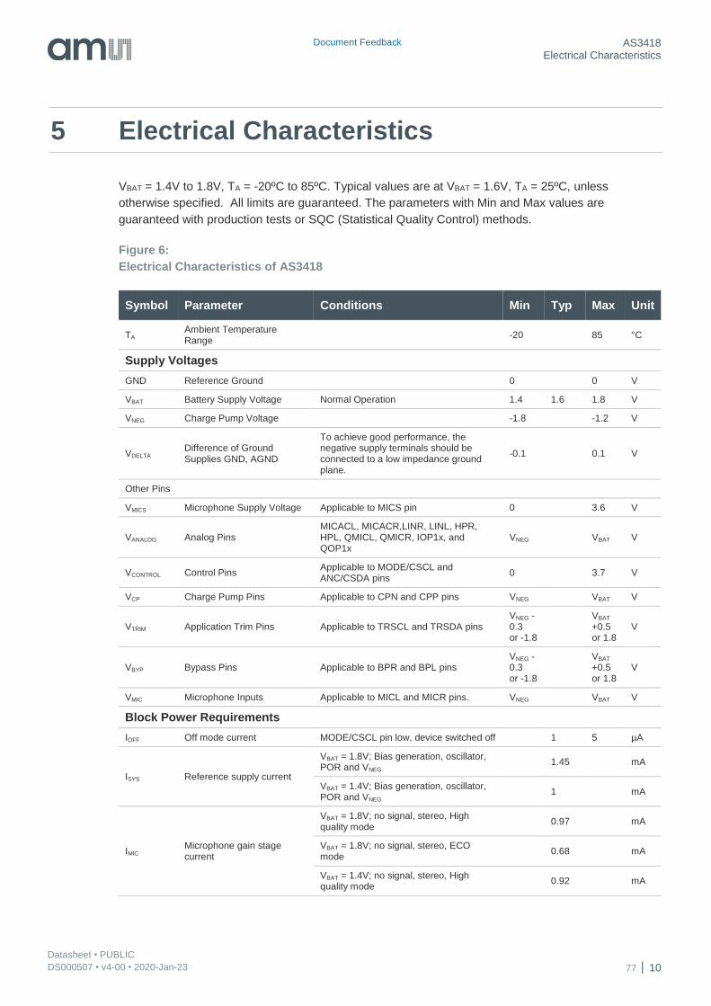
5 Electrical Characteristics
VBAT = 1.4V to 1.8V, TA = -20ºC to 85ºC. Typical values are at VBAT = 1.6V, TA = 25ºC, unless
otherwise specified. All limits are guaranteed. The parameters with Min and Max values are
guaranteed with production tests or SQC (Statistical Quality Control) methods.
Figure 6:
Electrical Characteristics of AS3418
Symbol Parameter Conditions Min Typ Max Unit
TA Ambient Temperature Range
-20 85 °C
Supply Voltages
GND Reference Ground 0 0 V
VBAT Battery Supply Voltage Normal Operation 1.4 1.6 1.8 V
VNEG Charge Pump Voltage -1.8 -1.2 V
VDELTA Difference of Ground Supplies GND, AGND
To achieve good performance, the negative supply terminals should be connected to a low impedance ground plane.
-0.1 0.1 V
Other Pins
VMICS Microphone Supply Voltage Applicable to MICS pin 0 3.6 V
VANALOG Analog Pins MICACL, MICACR,LINR, LINL, HPR, HPL, QMICL, QMICR, IOP1x, and QOP1x
VNEG VBAT V
VCONTROL Control Pins Applicable to MODE/CSCL and ANC/CSDA pins
0 3.7 V
VCP Charge Pump Pins Applicable to CPN and CPP pins VNEG VBAT V
VTRIM Application Trim Pins Applicable to TRSCL and TRSDA pins VNEG -0.3 or -1.8
VBAT +0.5 or 1.8
V
VBYP Bypass Pins Applicable to BPR and BPL pins VNEG -0.3 or -1.8
VBAT +0.5 or 1.8
V
VMIC Microphone Inputs Applicable to MICL and MICR pins. VNEG VBAT V
Block Power Requirements
IOFF Off mode current MODE/CSCL pin low, device switched off 1 5 µA
ISYS Reference supply current
VBAT = 1.8V; Bias generation, oscillator, POR and VNEG
1.45 mA
VBAT = 1.4V; Bias generation, oscillator, POR and VNEG
1 mA
IMIC Microphone gain stage current
VBAT = 1.8V; no signal, stereo, High quality mode
0.97 mA
VBAT = 1.8V; no signal, stereo, ECO mode
0.68 mA
VBAT = 1.4V; no signal, stereo, High quality mode
0.92 mA
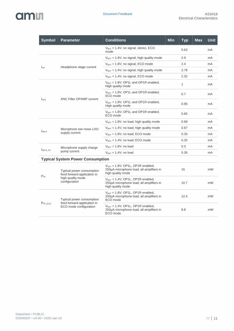
Document Feedback AS3418 Electrical Characteristics
Datasheet • PUBLIC DS000507 • v4-00 • 2020-Jan-23 77 11
Symbol Parameter Conditions Min Typ Max Unit
VBAT = 1.4V; no signal, stereo, ECO mode
0.63 mA
IHP Headphone stage current
VBAT = 1.8V; no signal, high quality mode 2.9 mA
VBAT = 1.8V; no signal, ECO mode 2.4 mA
VBAT = 1.4V; no signal, high quality mode 2.78 mA
VBAT = 1.4V; no signal, ECO mode 2.32 mA
IOP1 ANC Filter OPAMP current
VBAT = 1.8V; OP1L and OP1R enabled, High quality mode
1 mA
VBAT = 1.8V; OP1L and OP1R enabled, ECO mode
0.7 mA
VBAT = 1.8V; OP1L and OP1R enabled, High quality mode
0.95 mA
VBAT = 1.8V; OP1L and OP1R enabled, ECO mode
0.65 mA
IMICS Microphone low noise LDO supply current
VBAT = 1.8V; no load; high quality mode 0.69 mA
VBAT = 1.4V; no load; high quality mode 0.67 mA
VBAT = 1.8V; no load; ECO mode 0.33 mA
VBAT = 1.4V; no load; ECO mode 0.32 mA
IMICS_CP Microphone supply charge pump current
VBAT = 1.8V; no load 0.3 mA
VBAT = 1.4V; no load 0.26 mA
Typical System Power Consumption
PFF
Typical power consumption feed forward application in high quality mode configuration
VBAT = 1.8V; OP1L, OP1R enabled, 250µA microphone load; all amplifiers in high quality mode
15 mW
VBAT = 1.4V; OP1L, OP1R enabled, 250µA microphone load; all amplifiers in high quality mode
10.7 mW
PFF_ECO Typical power consumption feed forward application in ECO mode configuration
VBAT = 1.8V; OP1L, OP1R enabled, 250µA microphone load; all amplifiers in ECO mode
12.4 mW
VBAT = 1.4V; OP1L, OP1R enabled, 250µA microphone load; all amplifiers in ECO mode
8.8 mW
Document Feedback AS3418 Functional Description
Datasheet • PUBLIC DS000507 • v4-00 • 2020-Jan-23 77 12
6 Functional Description
This section provides a detailed description of the device related components.
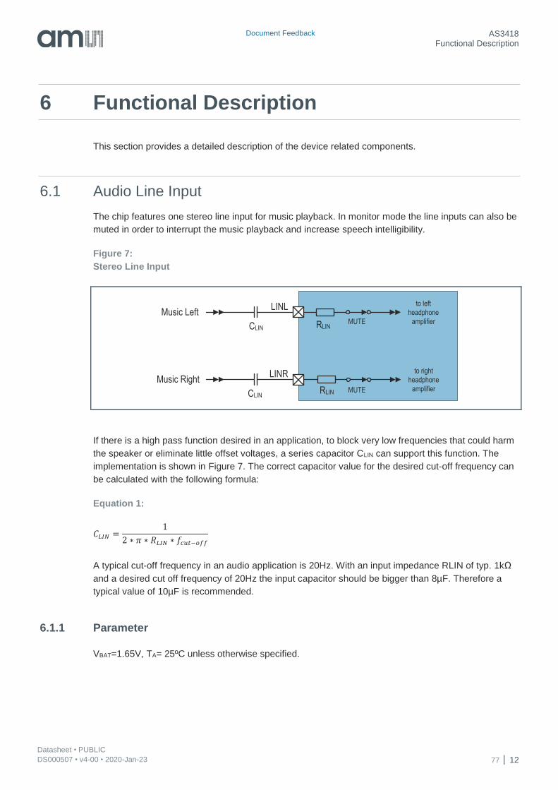
6.1 Audio Line Input
The chip features one stereo line input for music playback. In monitor mode the line inputs can also be
muted in order to interrupt the music playback and increase speech intelligibility.
Figure 7:
Stereo Line Input
If there is a high pass function desired in an application, to block very low frequencies that could harm
the speaker or eliminate little offset voltages, a series capacitor CLIN can support this function. The
implementation is shown in Figure 7. The correct capacitor value for the desired cut-off frequency can
be calculated with the following formula:
Equation 1:
𝐶𝐿𝐼𝑁 =1
2 ∗ 𝜋 ∗ 𝑅𝐿𝐼𝑁 ∗ 𝑓𝑐𝑢𝑡−𝑜𝑓𝑓
A typical cut-off frequency in an audio application is 20Hz. With an input impedance RLIN of typ. 1kΩ
and a desired cut off frequency of 20Hz the input capacitor should be bigger than 8µF. Therefore a
typical value of 10µF is recommended.
6.1.1 Parameter
VBAT=1.65V, TA= 25ºC unless otherwise specified.
to left
headphone
amplifierMUTE
to right
headphone
amplifierMUTE
Music LeftLINL
Music RightLINR
RLIN
RLIN
CLIN
CLIN
Document Feedback AS3418 Functional Description
Datasheet • PUBLIC DS000507 • v4-00 • 2020-Jan-23 77 13
Figure 8:
Parameter of Line Input
Symbol Parameter Conditions Min Typ Max Unit
VLIN Input Signal Level VBAT*0.9
VBAT VPEAK
RLIN Input Impedance 1 kΩ
AMUTE Mute Attenuation 100 dB
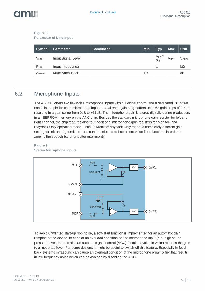
6.2 Microphone Inputs
The AS3418 offers two low noise microphone inputs with full digital control and a dedicated DC offset
cancellation pin for each microphone input. In total each gain stage offers up to 63 gain steps of 0.5dB
resulting in a gain range from 0dB to +31dB. The microphone gain is stored digitally during production,
in an EEPROM memory on the ANC chip. Besides the standard microphone gain register for left and
right channel, the chip features also four additional microphone gain registers for Monitor- and
Playback Only operation mode. Thus, in Monitor/Playback Only mode, a completely different gain
setting for left and right microphone can be selected to implement voice filter functions in order to
amplify the speech band for better intelligibility.
Figure 9:
Stereo Microphone Inputs
To avoid unwanted start-up pop noise, a soft-start function is implemented for an automatic gain
ramping of the device. In case of an overload condition on the microphone input (e.g. high sound
pressure level) there is also an automatic gain control (AGC) function available which reduces the gain
to a moderate level. For some designs it might be useful to switch off this feature. Especially in feed-
back systems infrasound can cause an overload condition of the microphone preamplifier that results
in low frequency noise which can be avoided by disabling the AGC.
MUTE
MUTE
AGCMICL
MICR
MICACL
MICACR
QMICL
QMICRAGC
DISCHARGE
DISCHARGE
Document Feedback AS3418 Functional Description
Datasheet • PUBLIC DS000507 • v4-00 • 2020-Jan-23 77 14
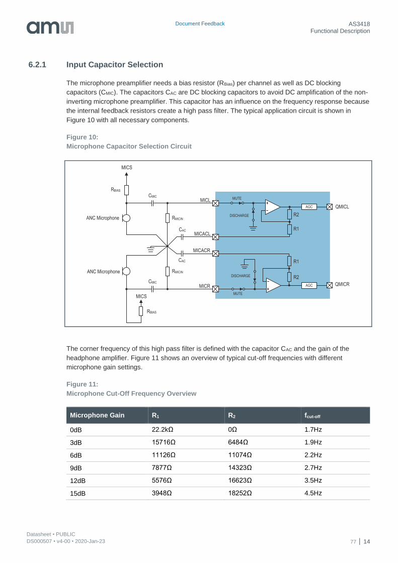
6.2.1 Input Capacitor Selection
The microphone preamplifier needs a bias resistor (RBias) per channel as well as DC blocking
capacitors (CMIC). The capacitors CAC are DC blocking capacitors to avoid DC amplification of the non-
inverting microphone preamplifier. This capacitor has an influence on the frequency response because
the internal feedback resistors create a high pass filter. The typical application circuit is shown in
Figure 10 with all necessary components.
Figure 10:
Microphone Capacitor Selection Circuit
The corner frequency of this high pass filter is defined with the capacitor CAC and the gain of the
headphone amplifier. Figure 11 shows an overview of typical cut-off frequencies with different
microphone gain settings.
Figure 11:
Microphone Cut-Off Frequency Overview
Microphone Gain R1 R2 fcut-off
0dB 22.2kΩ 0Ω 1.7Hz
3dB 15716Ω 6484Ω 1.9Hz
6dB 11126Ω 11074Ω 2.2Hz
9dB 7877Ω 14323Ω 2.7Hz
12dB 5576Ω 16623Ω 3.5Hz
15dB 3948Ω 18252Ω 4.5Hz
MUTE
MUTE
AGC
AGC
MICL
MICR
MICACL
MICACR
QMICL
QMICR
CMIC
CMIC
RBIAS
RBIAS
RMICIN
RMICIN
CAC
CAC
MICS
MICS
ANC Microphone
ANC MicrophoneDISCHARGE
DISCHARGE R2
R1
R2
R1
Document Feedback AS3418 Functional Description
Datasheet • PUBLIC DS000507 • v4-00 • 2020-Jan-23 77 15
Microphone Gain R1 R2 fcut-off
18dB 2795Ω 19405Ω 6.1Hz
21dB 1979Ω 20221Ω 8.4Hz
24dB 1400Ω 20800Ω 11.5Hz
27dB 992Ω 21208Ω 16.3Hz
30dB 702Ω 21498Ω 22.7Hz
It is important when doing the ANC filter simulations to include all microphone filter components to
incorporate the gain and phase influence of these components. In the cut-off frequency overview,
capacitor CAC was defined as 10µF which results in a rather low cut-off frequency for best ANC filter
design. If a different capacitor value is desired in the application, the following formula defines the
transfer function of the high pass circuit of the microphone preamplifier:
Equation 2:
|𝐴| =√4 ∗ 𝐶𝐴𝐶
2 ∗ 𝑓2 ∗ (𝑅1 + 𝑅2)2 ∗ 𝜋2 + 1
√4 ∗ 𝐶𝐴𝐶2 ∗ 𝑓2 ∗ 𝑅1
2 ∗ 𝜋2 + 1
The simplified transfer function does not include the high pass filter defined by CMIC and RMICIN.
With the recommended values of 2.2µF for CMIC and 22kΩ for RMICIN this filter can be neglected
because of the very low cut-off frequency of 1.5Hz. The cut-off frequency for this filter can be
calculated with the following formula:
Equation 3:
𝑓𝑐𝑢𝑡−𝑜𝑓𝑓 =1
2 ∗ 𝜋 ∗ 𝑅𝑀𝐼𝐶𝐼𝑁 ∗ 𝐶𝑀𝐼𝐶
The simulated frequency response for the microphone preamplifier with the recommended component
values is shown in Figure 12.
Document Feedback AS3418 Functional Description
Datasheet • PUBLIC DS000507 • v4-00 • 2020-Jan-23 77 16
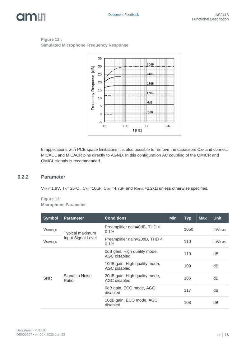
Figure 12 :
Simulated Microphone Frequency Response
In applications with PCB space limitations it is also possible to remove the capacitors CAC and connect
MICACL and MICACR pins directly to AGND. In this configuration AC coupling of the QMICR and
QMICL signals is recommended.
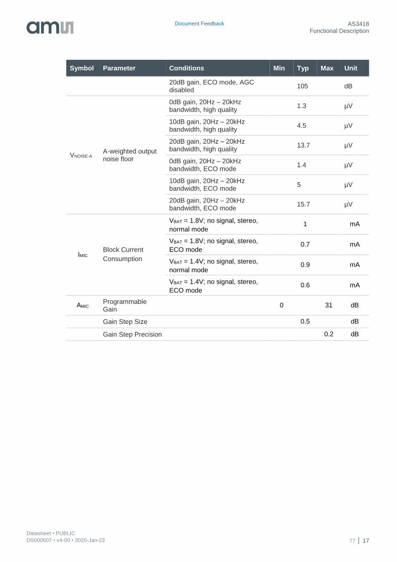
6.2.2 Parameter
VBAT=1.8V, TA= 25ºC , CAC=10µF, CMIC=4.7µF and RMICIN=2.2kΩ unless otherwise specified.
Figure 13:
Microphone Parameter
Symbol Parameter Conditions Min Typ Max Unit
VMICIN_0 Typical maximum Input Signal Level
Preamplifier gain=0dB, THD < 0.1%
1050 mVRMS
VMICIN_0 Preamplifier gain=20dB, THD < 0.1%
110 mVRMS
SNR Signal to Noise Ratio
0dB gain, High quality mode, AGC disabled
119 dB
10dB gain, High quality mode, AGC disabled
109 dB
20dB gain, High quality mode, AGC disabled
106 dB
0dB gain, ECO mode, AGC disabled
117 dB
10dB gain, ECO mode, AGC disabled
108 dB
-5
0
5
10
15
20
25
30
35
10 100 1k 10k
Fre
qu
en
cy R
esp
on
se
[d
B]
f [Hz]
0dB
6dB
12dB
18dB
24dB
30dB
Document Feedback AS3418 Functional Description
Datasheet • PUBLIC DS000507 • v4-00 • 2020-Jan-23 77 17
Symbol Parameter Conditions Min Typ Max Unit
20dB gain, ECO mode, AGC disabled
105 dB
VNOISE-A A-weighted output noise floor
0dB gain, 20Hz – 20kHz bandwidth, high quality
1.3 µV
10dB gain, 20Hz – 20kHz bandwidth, high quality
4.5 µV
20dB gain, 20Hz – 20kHz bandwidth, high quality
13.7 µV
0dB gain, 20Hz – 20kHz bandwidth, ECO mode
1.4 µV
10dB gain, 20Hz – 20kHz bandwidth, ECO mode
5 µV
20dB gain, 20Hz – 20kHz bandwidth, ECO mode
15.7 µV
IMIC Block Current
Consumption
VBAT = 1.8V; no signal, stereo,
normal mode 1 mA
VBAT = 1.8V; no signal, stereo,
ECO mode 0.7 mA
VBAT = 1.4V; no signal, stereo,
normal mode 0.9 mA
VBAT = 1.4V; no signal, stereo,
ECO mode 0.6 mA
AMIC Programmable Gain
0 31 dB
Gain Step Size 0.5 dB
Gain Step Precision 0.2 dB
Document Feedback AS3418 Functional Description
Datasheet • PUBLIC DS000507 • v4-00 • 2020-Jan-23 77 18
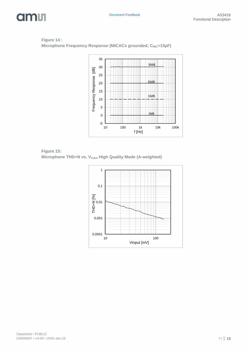
Figure 14 :
Microphone Frequency Response (MICACx grounded; CMIC=10µF)
Figure 15:
Microphone THD+N vs. Vinput High Quality Mode (A-weighted)
0,0001
0,001
0,01
0,1
1
10 100
TH
D+
N [%
]
Vinput [mV]
-5
0
5
10
15
20
25
30
35
10 100 1k 10k 100k
Fre
qu
en
cy R
esp
on
se
[d
B]
f [Hz]
0dB
30dB
10dB
20dB
Document Feedback AS3418 Functional Description
Datasheet • PUBLIC DS000507 • v4-00 • 2020-Jan-23 77 19
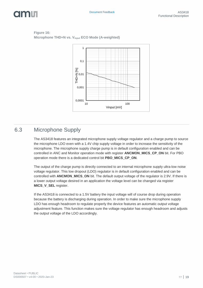
Figure 16:
Microphone THD+N vs. Vinput ECO Mode (A-weighted)
6.3 Microphone Supply
The AS3418 features an integrated microphone supply voltage regulator and a charge pump to source
the microphone LDO even with a 1.4V chip supply voltage in order to increase the sensitivity of the
microphone. The microphone supply charge pump is in default configuration enabled and can be
controlled in ANC and Monitor operation mode with register ANCMON_MICS_CP_ON bit. For PBO
operation mode there is a dedicated control bit PBO_MICS_CP_ON.
The output of the charge pump is directly connected to an internal microphone supply ultra-low noise
voltage regulator. This low dropout (LDO) regulator is in default configuration enabled and can be
controlled with ANCMON_MICS_ON bit. The default output voltage of the regulator is 2.9V. If there is
a lower output voltage desired in an application the voltage level can be changed via register
MICS_V_SEL register.
If the AS3418 is connected to a 1.5V battery the input voltage will of course drop during operation
because the battery is discharging during operation. In order to make sure the microphone supply
LDO has enough headroom to regulate properly the device features an automatic output voltage
adjustment feature. This function makes sure the voltage regulator has enough headroom and adjusts
the output voltage of the LDO accordingly.
0,0001
0,001
0,01
0,1
1
10 100
TH
D+
N [%
]
Vinput [mV]
Document Feedback AS3418 Functional Description
Datasheet • PUBLIC DS000507 • v4-00 • 2020-Jan-23 77 20
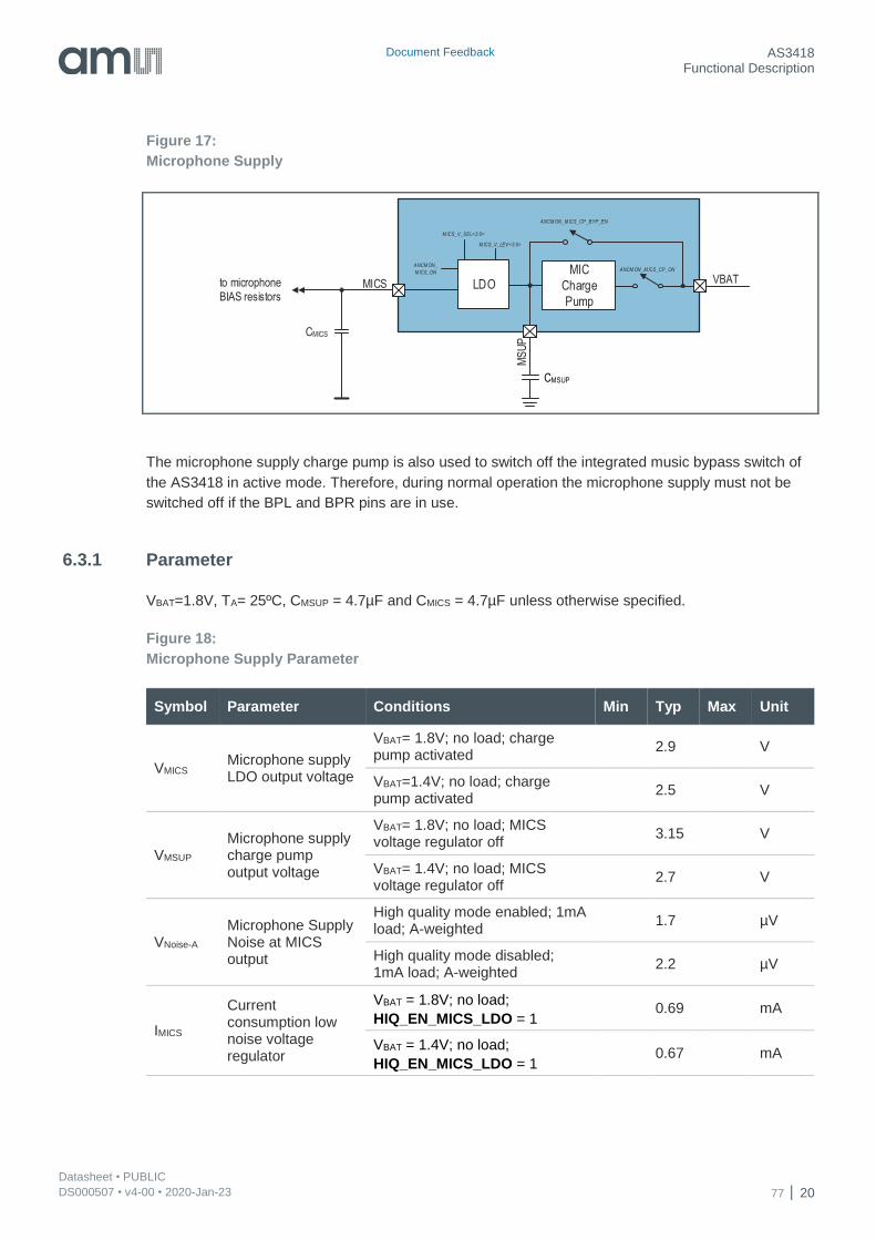
Figure 17:
Microphone Supply
The microphone supply charge pump is also used to switch off the integrated music bypass switch of
the AS3418 in active mode. Therefore, during normal operation the microphone supply must not be
switched off if the BPL and BPR pins are in use.
6.3.1 Parameter
VBAT=1.8V, TA= 25ºC, CMSUP = 4.7µF and CMICS = 4.7µF unless otherwise specified.
Figure 18:
Microphone Supply Parameter
Symbol Parameter Conditions Min Typ Max Unit
VMICS Microphone supply LDO output voltage
VBAT= 1.8V; no load; charge pump activated
2.9 V
VBAT=1.4V; no load; charge pump activated
2.5 V
VMSUP Microphone supply charge pump output voltage
VBAT= 1.8V; no load; MICS voltage regulator off
3.15 V
VBAT= 1.4V; no load; MICS voltage regulator off
2.7 V
VNoise-A Microphone Supply Noise at MICS output
High quality mode enabled; 1mA load; A-weighted
1.7 µV
High quality mode disabled; 1mA load; A-weighted
2.2 µV
IMICS
Current consumption low noise voltage regulator
VBAT = 1.8V; no load;
HIQ_EN_MICS_LDO = 1 0.69 mA
VBAT = 1.4V; no load;
HIQ_EN_MICS_LDO = 1 0.67 mA
MS
UP
CMSUP
MIC
Charge
Pump
VBATMICSto microphoneBIAS resistors
CMICS
LDO
ANCMON_
MICS_ONANCMON_MICS_CP_ON
ANCM ON_MICS_CP_BYP_EN
M ICS_V_SEL<3:0>
M ICS_V_LEV<3:0>
Document Feedback AS3418 Functional Description
Datasheet • PUBLIC DS000507 • v4-00 • 2020-Jan-23 77 21
Symbol Parameter Conditions Min Typ Max Unit
VBAT = 1.8V; no load;
HIQ_EN_MICS_LDO = 0 0.33 mA
VBAT = 1.4V; no load;
HIQ_EN_MICS_LDO = 0 0.32 mA
IMICS_CP
Current consumption microphone supply charge pump
VBAT= 1.8V; MICS voltage regulator off; no load
0.3 mA
VBAT= 1.8V; MICS voltage regulator off; 1mA load
3.5 mA
VBAT= 1.4V; MICS voltage regulator off; no load
0.26 mA
VBAT= 1.4V; MICS voltage regulator off; 1mA load
3.33 mA
IOUT Output current Charge pump activated 2 mA
Figure 19:
Microphone Supply Load Characteristic
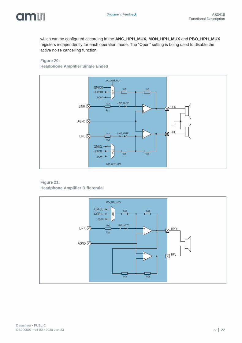
6.4 Headphone Amplifier
The headphone amplifier is a true ground output using VNEG as negative supply. It is designed to
feature an output power of 2x34mW @ 32Ωload. For higher output requirements, the headphone
amplifier is also capable of operating in bridged mode. In this mode the left output is carrying the
inverted signal of the right output shown in Figure 21. With a VBAT voltage of 1.8V, a maximum output
power of 100mW can be achieved. This is necessary for over- and on ear headsets with higher output
power requirements. The amplifier itself features various input sources. The line input signal is directly
connected to the headphone amplifier. The input multiplexer supports three different input signals
0
1
2
3
1 2 3 4
VM
ICS
[V]
Iload [mA]
VBAT=1,4V
VBAT=1.8V
Document Feedback AS3418 Functional Description
Datasheet • PUBLIC DS000507 • v4-00 • 2020-Jan-23 77 22
which can be configured according in the ANC_HPH_MUX, MON_HPH_MUX and PBO_HPH_MUX
registers independently for each operation mode. The “Open” setting is being used to disable the
active noise cancelling function.
Figure 20:
Headphone Amplifier Single Ended
Figure 21:
Headphone Amplifier Differential
MU
X
QMICR
QOP1R
open
MU
X
QMICL
QOP1L
open
HPR
HPL
LINL
AGND
LINRRLI N
RLI N
1kΩ 1kΩ
1kΩ 1kΩ
1kΩ
1kΩ
XXX_HPH_MUX
XXX_HPH_MUX
LINE_MUTE
LINE_MUTE
MU
X
QMICL
QOP1L
open
HPR
HPL
AGND
LINRRLI N
1k 1k
1k 1k
1k
XXX_HPH_MUX
LINE_MUTE
Document Feedback AS3418 Functional Description
Datasheet • PUBLIC DS000507 • v4-00 • 2020-Jan-23 77 23
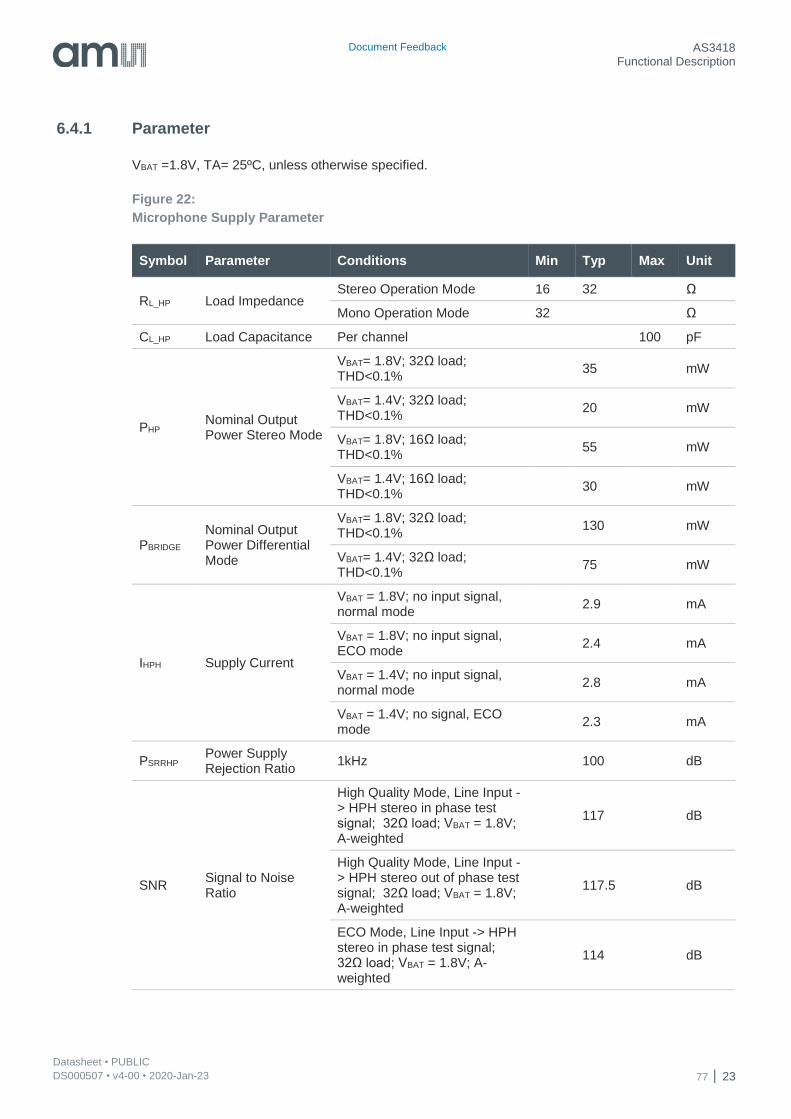
6.4.1 Parameter
VBAT =1.8V, TA= 25ºC, unless otherwise specified.
Figure 22:
Microphone Supply Parameter
Symbol Parameter Conditions Min Typ Max Unit
RL_HP Load Impedance Stereo Operation Mode 16 32 Ω
Mono Operation Mode 32 Ω
CL_HP Load Capacitance Per channel 100 pF
PHP Nominal Output Power Stereo Mode
VBAT= 1.8V; 32Ω load; THD<0.1%
35 mW
VBAT= 1.4V; 32Ω load; THD<0.1%
20 mW
VBAT= 1.8V; 16Ω load; THD<0.1%
55 mW
VBAT= 1.4V; 16Ω load; THD<0.1%
30 mW
PBRIDGE Nominal Output Power Differential Mode
VBAT= 1.8V; 32Ω load; THD<0.1%
130 mW
VBAT= 1.4V; 32Ω load; THD<0.1%
75 mW
IHPH Supply Current
VBAT = 1.8V; no input signal, normal mode
2.9 mA
VBAT = 1.8V; no input signal, ECO mode
2.4 mA
VBAT = 1.4V; no input signal, normal mode
2.8 mA
VBAT = 1.4V; no signal, ECO mode
2.3 mA
PSRRHP Power Supply Rejection Ratio
1kHz 100 dB
SNR Signal to Noise Ratio
High Quality Mode, Line Input -> HPH stereo in phase test signal; 32Ω load; VBAT = 1.8V; A-weighted
117 dB
High Quality Mode, Line Input -> HPH stereo out of phase test signal; 32Ω load; VBAT = 1.8V; A-weighted
117.5 dB
ECO Mode, Line Input -> HPH stereo in phase test signal; 32Ω load; VBAT = 1.8V; A-weighted
114 dB
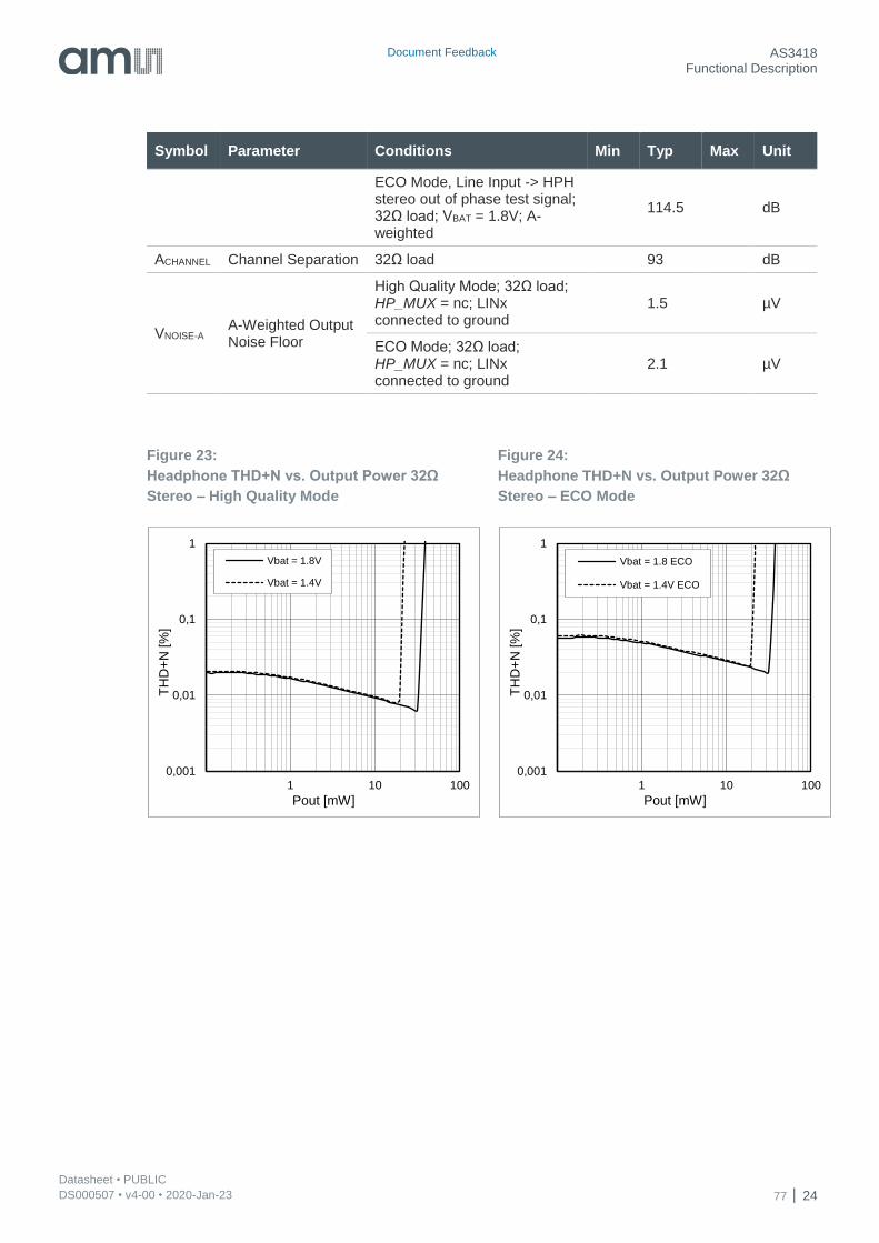
Document Feedback AS3418 Functional Description
Datasheet • PUBLIC DS000507 • v4-00 • 2020-Jan-23 77 24
Symbol Parameter Conditions Min Typ Max Unit
ECO Mode, Line Input -> HPH stereo out of phase test signal; 32Ω load; VBAT = 1.8V; A-weighted
114.5 dB
ACHANNEL Channel Separation 32Ω load 93 dB
VNOISE-A A-Weighted Output Noise Floor
High Quality Mode; 32Ω load; HP_MUX = nc; LINx connected to ground
1.5 µV
ECO Mode; 32Ω load; HP_MUX = nc; LINx connected to ground
2.1 µV
Figure 23:
Headphone THD+N vs. Output Power 32Ω
Stereo – High Quality Mode
Figure 24:
Headphone THD+N vs. Output Power 32Ω
Stereo – ECO Mode
0,001
0,01
0,1
1
1 10 100
TH
D+
N [%
]
Pout [mW]
Vbat = 1.8V
Vbat = 1.4V
0,001
0,01
0,1
1
1 10 100
TH
D+
N [%
]
Pout [mW]
Vbat = 1.8 ECO
Vbat = 1.4V ECO
Document Feedback AS3418 Functional Description
Datasheet • PUBLIC DS000507 • v4-00 • 2020-Jan-23 77 25
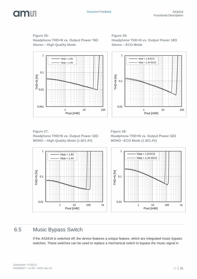
Figure 25:
Headphone THD+N vs. Output Power 16Ω
Stereo – High Quality Mode
Figure 26:
Headphone THD+N vs. Output Power 16Ω
Stereo – ECO Mode
Figure 27:
Headphone THD+N vs. Output Power 32Ω
MONO – High Quality Mode (1.8//1.4V)
Figure 28:
Headphone THD+N vs. Output Power 32Ω
MONO –ECO Mode (1.8//1.4V)
6.5 Music Bypass Switch
If the AS3418 is switched off, the device features a unique feature, which are integrated music bypass
switches. These switches can be used to replace a mechanical switch to bypass the music signal in
0,001
0,01
0,1
1
1 10 100
TH
D+
N [%
]
Pout [mW]
Vbat = 1.8V
Vbat = 1.4V
0,01
0,1
1
1 10 100
TH
D+
N [%
]Pout [mW]
Vbat = 1.8 ECO
Vbat = 1.4V ECO
0,01
0,1
1
1 10 100 1k
TH
D+
N [%
]
Pout [mW]
Vbat = 1.8V
Vbat = 1.4V
0,01
0,1
1
1 10 100 1k
TH
D+
N [%
]
Pout [mW]
Vbat = 1.8 ECO
Vbat = 1.4V ECO
Document Feedback AS3418 Functional Description
Datasheet • PUBLIC DS000507 • v4-00 • 2020-Jan-23 77 26
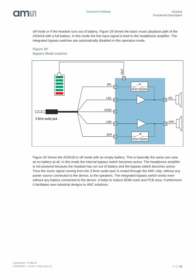
off mode or if the headset runs out of battery. Figure 29 shows the basic music playback path of the
AS3418 with a full battery. In this mode the line input signal is feed to the headphone amplifier. The
integrated bypass switches are automatically disabled in this operation mode.
Figure 29:
Bypass Mode Inactive
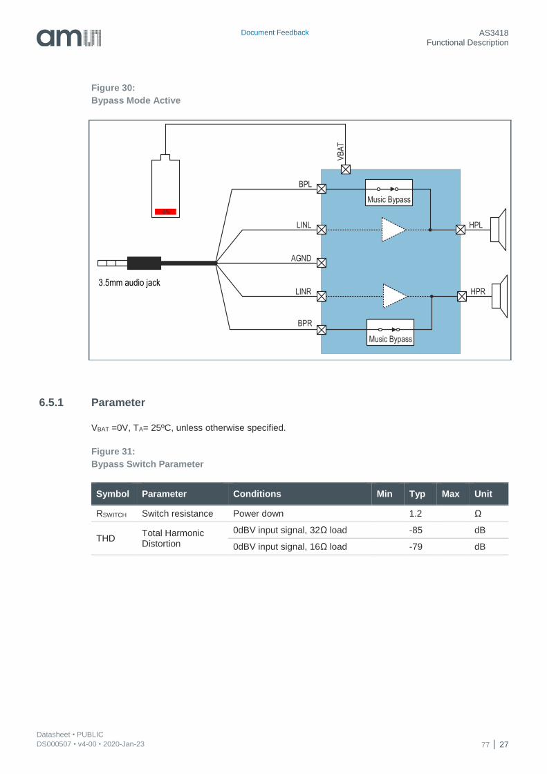
Figure 30 shows the AS3418 in off mode with an empty battery. This is basically the same use case
as no battery at all. In this mode the internal bypass switch becomes active. The headphone amplifier
is not powered because the headset has run out of battery and the bypass switch becomes active.
Thus the music signal coming from the 3.5mm audio jack is routed through the ANC chip, without any
power source connected to the device, to the speakers. The integrated bypass switch works even
without any battery connected to the device. It helps to reduce BOM costs and PCB area. Furthermore
it facilitates new industrial designs to ANC solutions.
Music Bypass
Music Bypass
BPL
BPR
AGND
LINL
LINR
100%
3.5mm audio jackHPR
HPL
VB
AT
Document Feedback AS3418 Functional Description
Datasheet • PUBLIC DS000507 • v4-00 • 2020-Jan-23 77 27
Figure 30:
Bypass Mode Active
6.5.1 Parameter
VBAT =0V, TA= 25ºC, unless otherwise specified.
Figure 31:
Bypass Switch Parameter
Symbol Parameter Conditions Min Typ Max Unit
RSWITCH Switch resistance Power down 1.2 Ω
THD Total Harmonic Distortion
0dBV input signal, 32Ω load -85 dB
0dBV input signal, 16Ω load -79 dB
Music Bypass
Music Bypass
BPL
BPR
AGND
LINL
LINR
0%
3.5mm audio jackHPR
HPL
VB
AT
Document Feedback AS3418 Functional Description
Datasheet • PUBLIC DS000507 • v4-00 • 2020-Jan-23 77 28
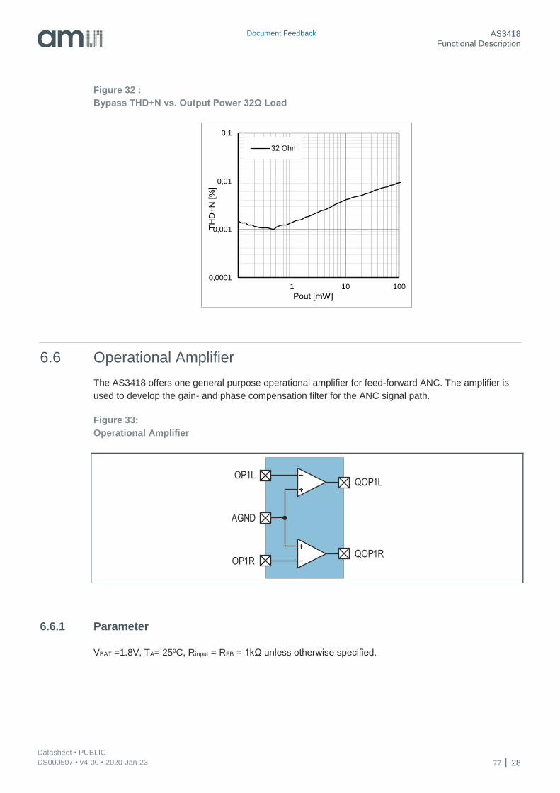
Figure 32 :
Bypass THD+N vs. Output Power 32Ω Load
6.6 Operational Amplifier
The AS3418 offers one general purpose operational amplifier for feed-forward ANC. The amplifier is
used to develop the gain- and phase compensation filter for the ANC signal path.
Figure 33:
Operational Amplifier
6.6.1 Parameter
VBAT =1.8V, TA= 25ºC, Rinput = RFB = 1kΩ unless otherwise specified.
0,0001
0,001
0,01
0,1
1 10 100
TH
D+
N [%
]
Pout [mW]
32 Ohm
AGND
OP1L
OP1RQOP1R
QOP1L
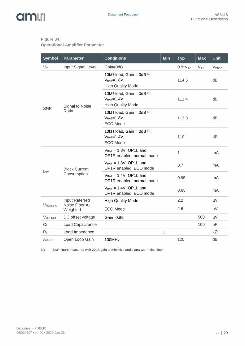
Document Feedback AS3418 Functional Description
Datasheet • PUBLIC DS000507 • v4-00 • 2020-Jan-23 77 29
Figure 34:
Operational Amplifier Parameter
Symbol Parameter Conditions Min Typ Max Unit
VIN Input Signal Level Gain=0dB 0.9*VBAT VBAT VPEAK
SNR Signal to Noise Ratio
10k load Gain = 0dB (1),
VBAT=1.8V,
High Quality Mode
114.5 dB
10k load Gain = 0dB (1),
VBAT=1.4V
High Quality Mode
111.4 dB
10k load Gain = 0dB (1),
VBAT=1.8V,
ECO Mode
113.3 dB
10k load Gain = 0dB (1),
VBAT=1.4V,
ECO Mode
110 dB
IOP1 Block Current Consumption
VBAT = 1.8V; OP1L and
OP1R enabled; normal mode 1 mA
VBAT = 1.8V; OP1L and
OP1R enabled; ECO mode 0.7 mA
VBAT = 1.4V; OP1L and
OP1R enabled; normal mode 0.95 mA
VBAT = 1.4V; OP1L and
OP1R enabled; ECO mode 0.65 mA
VNOISE-A Input Referred Noise Floor A-Weighted
High Quality Mode 2.2 µV
ECO Mode 2.6 µV
VOFFSET DC offset voltage Gain=0dB 500 µV
CL Load Capacitance 100 pF
RL Load Impedance 1 kΩ
ALOOP Open Loop Gain 100MHz 120 dB
(1) SNR figure measured with 20dB gain to minimize audio analyzer noise floor
Document Feedback AS3418 Functional Description
Datasheet • PUBLIC DS000507 • v4-00 • 2020-Jan-23 77 30
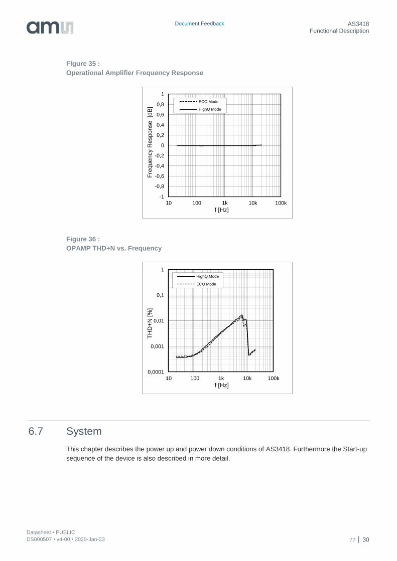
Figure 35 :
Operational Amplifier Frequency Response
Figure 36 :
OPAMP THD+N vs. Frequency
6.7 System
This chapter describes the power up and power down conditions of AS3418. Furthermore the Start-up
sequence of the device is also described in more detail.
-1
-0,8
-0,6
-0,4
-0,2
0
0,2
0,4
0,6
0,8
1
10 100 1k 10k 100k
Fre
qu
en
cy R
esp
on
se
[d
B]
f [Hz]
ECO Mode
HighQ Mode
0,0001
0,001
0,01
0,1
1
10 100 1k 10k 100k
TH
D+
N [%
]
f [Hz]
HighQ Mode
ECO Mode
Document Feedback AS3418 Functional Description
Datasheet • PUBLIC DS000507 • v4-00 • 2020-Jan-23 77 31
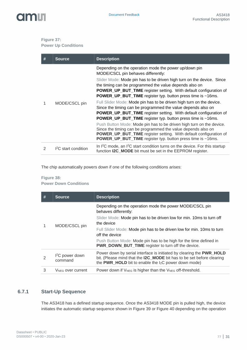
Figure 37:
Power Up Conditions
# Source Description
1 MODE/CSCL pin
Depending on the operation mode the power up/down pin
MODE/CSCL pin behaves differently:
Slider Mode: Mode pin has to be driven high turn on the device. Since
the timing can be programmed the value depends also on
POWER_UP_BUT_TIME register setting. With default configuration of
POWER_UP_BUT_TIME register typ. button press time is ~16ms.
Full Slider Mode: Mode pin has to be driven high turn on the device.
Since the timing can be programmed the value depends also on
POWER_UP_BUT_TIME register setting. With default configuration of
POWER_UP_BUT_TIME register typ. button press time is ~16ms.
Push Button Mode: Mode pin has to be driven high turn on the device. Since the timing can be programmed the value depends also on POWER_UP_BUT_TIME register setting. With default configuration of POWER_UP_BUT_TIME register typ. button press time is ~16ms.
2 I2C start condition In I2C mode, an I2C start condition turns on the device. For this startup function I2C_MODE bit must be set in the EEPROM register.
The chip automatically powers down if one of the following conditions arises:
Figure 38:
Power Down Conditions
# Source Description
1 MODE/CSCL pin
Depending on the operation mode the power MODE/CSCL pin
behaves differently:
Slider Mode: Mode pin has to be driven low for min. 10ms to turn off
the device
Full Slider Mode: Mode pin has to be driven low for min. 10ms to turn
off the device
Push Button Mode: Mode pin has to be high for the time defined in PWR_DOWN_BUT_TIME register to turn off the device.
2 I2C power down command
Power down by serial interface is initiated by clearing the PWR_HOLD bit. (Please mind that the I2C_MODE bit has to be set before clearing the PWR_HOLD bit to enable the I2C power down mode)
3 VNEG over current Power down if VNEG is higher than the VNEG off-threshold.
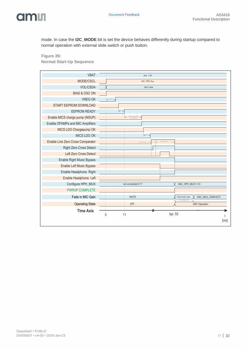
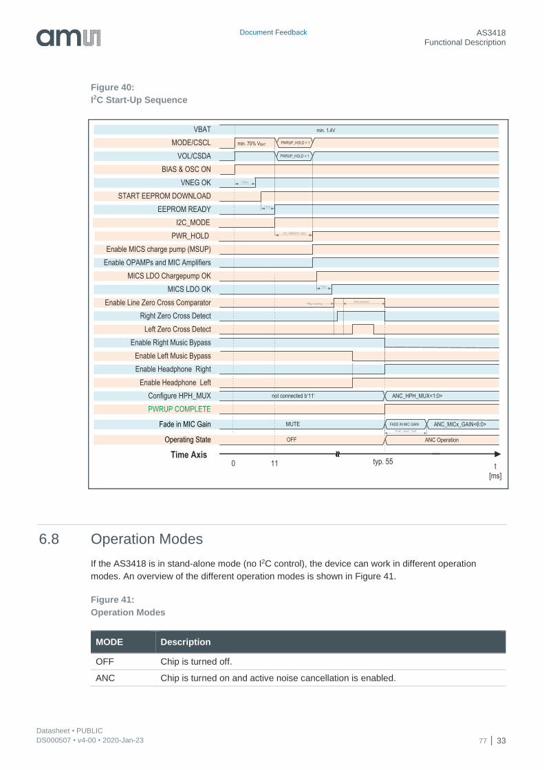
6.7.1 Start-Up Sequence
The AS3418 has a defined startup sequence. Once the AS3418 MODE pin is pulled high, the device
initiates the automatic startup sequence shown in Figure 39 or Figure 40 depending on the operation
Document Feedback AS3418 Functional Description
Datasheet • PUBLIC DS000507 • v4-00 • 2020-Jan-23 77 32
mode. In case the I2C_MODE bit is set the device behaves differently during startup compared to
normal operation with external slide switch or push button.
Figure 39:
Normal Start-Up Sequence
MODE/CSCL
VOL/CSDA
VBAT
BIAS & OSC ON
VNEG OK
Enable OPAMPs and MIC Amplifiers
MICS LDO Chargepump OK
0 typ. 52
~ ~
Time Axist
[ms]
min. 1.4V
min. 70% VBAT
don‘t care
Enable MICS charge pump (MSUP)
11
Enable Right Music Bypass
~10ms
START EEPROM DOWNLOAD
EEPROM READY~1ms
PWR_UP_BUT_TIME
(5ms-2500ms)
MICS LDO OK~5ms
Enable Left Music Bypass
Enable Line Zero Cross Comparator ~40µs masking31ms timeout
Right Zero Cross Detect
Left Zero Cross Detect
Enable Headphone Right
Enable Headphone Left
Configure HPH_MUX not connected b‘11‘ ANC_HPH_MUX<1:0>
PWRUP COMPLETE
Fade in MIC Gain MUTE FADE IN MIC GAIN ANC_MICx_GAIN<6:0>START_RAMP_TIME
Operating State ANC OperationOFF
Document Feedback AS3418 Functional Description
Datasheet • PUBLIC DS000507 • v4-00 • 2020-Jan-23 77 33
Figure 40:
I2C Start-Up Sequence
6.8 Operation Modes
If the AS3418 is in stand-alone mode (no I2C control), the device can work in different operation
modes. An overview of the different operation modes is shown in Figure 41.
Figure 41:
Operation Modes
MODE Description
OFF Chip is turned off.
ANC Chip is turned on and active noise cancellation is enabled.
MODE/CSCL
VOL/CSDA
VBAT
BIAS & OSC ON
VNEG OK
Enable OPAMPs and MIC Amplifiers
MICS LDO Chargepump OK
0 typ. 55
~ ~
Time Axist
[ms]
min. 1.4V
min. 70% VBAT
PWRUP_HOLD = 1
Enable MICS charge pump (MSUP)
11
Enable Right Music Bypass
~10ms
START EEPROM DOWNLOAD
EEPROM READY~1ms
I2C_TIMEOUT = 8ms
MICS LDO OK~5ms
Enable Left Music Bypass
Enable Line Zero Cross Comparator ~40µs masking31ms timeout
Right Zero Cross Detect
Left Zero Cross Detect
Enable Headphone Right
Enable Headphone Left
Configure HPH_MUX not connected b‘11‘ ANC_HPH_MUX<1:0>
PWRUP COMPLETE
Fade in MIC Gain MUTE FADE IN MIC GAIN ANC_MICx_GAIN<6:0>START_RAMP_TIME
Operating State ANC OperationOFF
I2C_MODE
PWR_HOLD
PWRUP_HOLD = 1
Document Feedback AS3418 Functional Description
Datasheet • PUBLIC DS000507 • v4-00 • 2020-Jan-23 77 34
MODE Description
MONITOR
In Monitor Mode, a different (normally higher) microphone preamplifier gain can be configured to get an amplification of the ambient noise. To get rid of the low pass filtering needed for the noise cancellation, the headphone input multiplexer can be set to a different (normally to MIC) source to increase speech intelligibility. In addition, the Line Input signal can be muted for further improved intelligibility. If the device is operated in I2C mode, it is also possible to enter the monitor mode by setting the MON_MODE_EN bit in register 0x03.
PBO
The Playback Only mode is a special mode that disables the noise cancelling function and just keeps e.g. line input amplifier or headphone amplifier active. Certainly this operation mode can also be used as an alternative Monitor or ANC mode with different gain settings.
With the AS3418 design engineers have different options to enter the described operation modes
shown in Figure 41. In addition to the different user interface modes described in the following three
chapters, it is also important to configure the device accordingly. Figure 42 shows the required register
configuration settings to enable the different AS3418 control modes.
Figure 42:
User Interface Control Modes
MODE Register UI_MODE<1:0>
Button Mode 0 0
Slider Mode 0 1
Full Slider Mode 1 0
Do not use 1 1
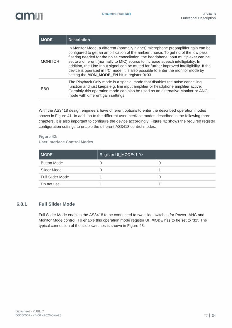
6.8.1 Full Slider Mode
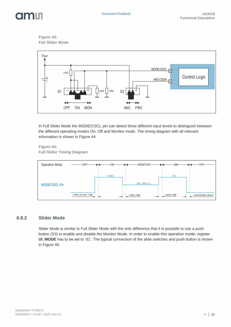
Full Slider Mode enables the AS3418 to be connected to two slide switches for Power, ANC and
Monitor Mode control. To enable this operation mode register UI_MODE has to be set to ‘d2’. The
typical connection of the slide switches is shown in Figure 43.
Document Feedback AS3418 Functional Description
Datasheet • PUBLIC DS000507 • v4-00 • 2020-Jan-23 77 35
Figure 43:
Full Slider Mode
In Full Slider Mode the MODE/CSCL pin can detect three different input levels to distinguish between
the different operating modes On, Off and Monitor mode. The timing diagram with all relevant
information is shown in Figure 44.
Figure 44:
Full Slider Timing Diagram
6.8.2 Slider Mode
Slider Mode is similar to Full Slider Mode with the only difference that it is possible to use a push
button (S3) to enable and disable the Monitor Mode. In order to enable this operation mode, register
UI_MODE has to be set to ‘d1’. The typical connection of the slide switches and push button is shown
in Figure 45.
MODE/CSCL
ANC/CSDAControl Logic
VBAT
22kΩ
22kΩ
OFF ON MON ANC PBO
S1 S21MΩ
MODE/CSCL Pin
OFF ON MONITOR ON OFF
> PWR_UP_BUT_TIME > MON_TIME > SHUTDOWN_DELAY
>=1.65V VBAT
45% - 55% VBAT
Operation Mode
> MON_TIME
Document Feedback AS3418 Functional Description
Datasheet • PUBLIC DS000507 • v4-00 • 2020-Jan-23 77 36
Figure 45:
Slider Mode
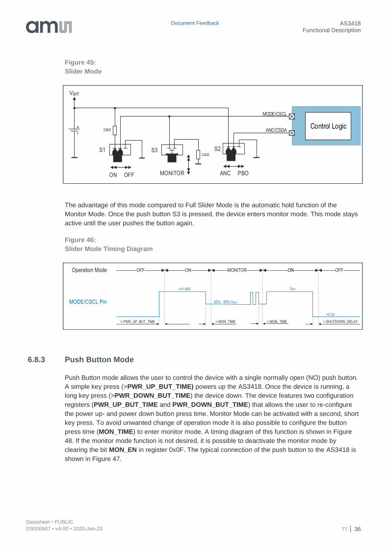
The advantage of this mode compared to Full Slider Mode is the automatic hold function of the
Monitor Mode. Once the push button S3 is pressed, the device enters monitor mode. This mode stays
active until the user pushes the button again.
Figure 46:
Slider Mode Timing Diagram
6.8.3 Push Button Mode
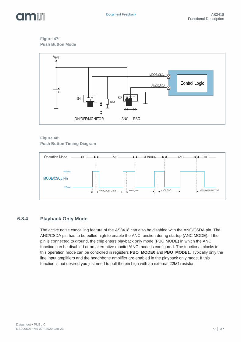
Push Button mode allows the user to control the device with a single normally open (NO) push button.
A simple key press (>PWR_UP_BUT_TIME) powers up the AS3418. Once the device is running, a
long key press (>PWR_DOWN_BUT_TIME) the device down. The device features two configuration
registers (PWR_UP_BUT_TIME and PWR_DOWN_BUT_TIME) that allows the user to re-configure
the power up- and power down button press time. Monitor Mode can be activated with a second, short
key press. To avoid unwanted change of operation mode it is also possible to configure the button
press time (MON_TIME) to enter monitor mode. A timing diagram of this function is shown in Figure
48. If the monitor mode function is not desired, it is possible to deactivate the monitor mode by
clearing the bit MON_EN in register 0x0F. The typical connection of the push button to the AS3418 is
shown in Figure 47.
MODE/CSCL
ANC/CSDAControl Logic
VBAT
22kΩ
ON OFF ANC PBO
S1 S222kΩ
MONITOR
S3
MODE/CSCL Pin
OFF ON MONITOR ON OFF
>=1.65V VBAT
45% - 55% VBAT
Operation Mode
<0.3V
> PWR_UP_BUT_TIME > MON_TIME > MON_TIME > SHUTDOWN_DELAY
Document Feedback AS3418 Functional Description
Datasheet • PUBLIC DS000507 • v4-00 • 2020-Jan-23 77 37
Figure 47:
Push Button Mode
Figure 48:
Push Button Timing Diagram
6.8.4 Playback Only Mode
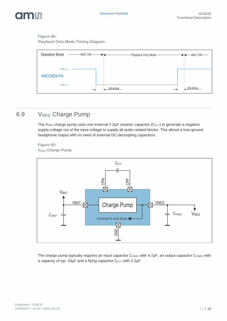
The active noise cancelling feature of the AS3418 can also be disabled with the ANC/CSDA pin. The
ANC/CSDA pin has to be pulled high to enable the ANC function during startup (ANC MODE). If the
pin is connected to ground, the chip enters playback only mode (PBO MODE) in which the ANC
function can be disabled or an alternative monitor/ANC mode is configured. The functional blocks in
this operation mode can be controlled in registers PBO_MODE0 and PBO_MODE1. Typically only the
line input amplifiers and the headphone amplifier are enabled in the playback only mode. If this
function is not desired you just need to pull the pin high with an external 22kΩ resistor.
MODE/CSCL
ANC/CSDAControl Logic
VBAT
ANC PBO
S222k
ON/OFF/MONITOR
S4
MODE/CSCL Pin
OFF ANC MONITOR ANC OFF
> PWR_UP_BUT_TIME
>65% VBAT
<35% VBAT
Operation Mode
> MON_TIME >PWR_DOWN_BUT_TIME> MON_TIME
Document Feedback AS3418 Functional Description
Datasheet • PUBLIC DS000507 • v4-00 • 2020-Jan-23 77 38
Figure 49:
Playback Only Mode Timing Diagram
6.9 VNEG Charge Pump
The VNEG charge pump uses one external 2.2µF ceramic capacitor (CFLY) to generate a negative
supply voltage out of the input voltage to supply all audio related blocks. This allows a true-ground
headphone output with no need of external DC-decoupling capacitors.
Figure 50:
VNEG Charge Pump
The charge pump typically requires an input capacitor CVBAT with 4.7µF, an output capacitor CVNEG with
a capacity of typ. 10µF and a flying capacitor CFLY with 2.2µF.
ANC/CSDA Pin
ANC ON Playback Only Mode ANC ON
200-400ms 200-400ms
>65% VBAT
<35% VBAT
Operation Mode
Charge Pump
Connection to audio blocks
GN
D
VBAT
VBAT VNEG
VNEGCVNEGCVBAT
CP
N
CP
P
CFLY
Document Feedback AS3418 Functional Description
Datasheet • PUBLIC DS000507 • v4-00 • 2020-Jan-23 77 39
6.9.1 Parameter
VBAT =1.8V, TA= 25ºC, unless otherwise specified.
Figure 51:
VNEG Charge Pump Parameter
Symbol Parameter Conditions Min Typ Max Unit
VIN Input Voltage VBAT 1.4 1.6 1.8 V
VOUT Output Voltage VNEG -1.8 -1 V
CVBAT VBAT input capacitor
Effective capacitive value 1.6 4.7 5.46 µF
CVNEG VNEG output capacitor
Effective capacitive value 3.4 10 12 µF
CFLY Flying capacitor Effective capacitive value 0.97 2.2 2.86 µF
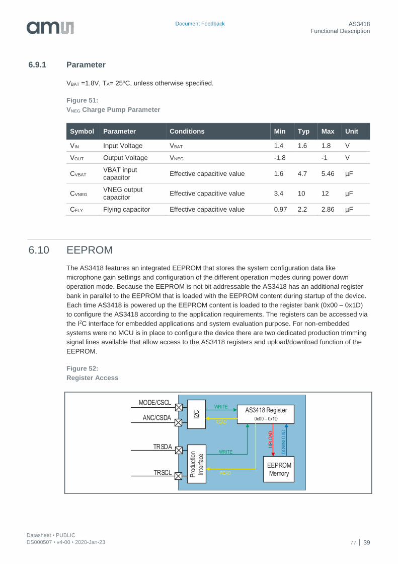
6.10 EEPROM
The AS3418 features an integrated EEPROM that stores the system configuration data like
microphone gain settings and configuration of the different operation modes during power down
operation mode. Because the EEPROM is not bit addressable the AS3418 has an additional register
bank in parallel to the EEPROM that is loaded with the EEPROM content during startup of the device.
Each time AS3418 is powered up the EEPROM content is loaded to the register bank (0x00 – 0x1D)
to configure the AS3418 according to the application requirements. The registers can be accessed via
the I2C interface for embedded applications and system evaluation purpose. For non-embedded
systems were no MCU is in place to configure the device there are two dedicated production trimming
signal lines available that allow access to the AS3418 registers and upload/download function of the
EEPROM.
Figure 52:
Register Access
I2C
Pro
duct
ion
Inte
rface
AS3418 Register0x00 – 0x1D
EEPROMMemory
WRITE
READ
WRITE
READ
UP
LO
AD
DO
WN
LOA
D
MODE/CSCL
ANC/CSDA
TRSDA
TRSCL
Document Feedback AS3418 Functional Description
Datasheet • PUBLIC DS000507 • v4-00 • 2020-Jan-23 77 40
The EEPROM supports three operation modes:
Upload Operation - The Upload function copies the register content of register 0x01 – 0x1D
and stores it permanently to the EEPROM.
Download Operation - The Download function copies the permanently stored EEPROM
content to the registers of AS3418 and overwrites the existing register content with the
EEPROM values like it happens during startup of the device.
TEST UPLOAD - The Test Upload function is a feature to trigger a test EEPROM upload.
During this test the device does not write the EEPROM settings, instead it just tries if it would be
possible to write the EEPROM successfully. It is recommended to perform this test each time
before a real EEPROM upload is triggered.
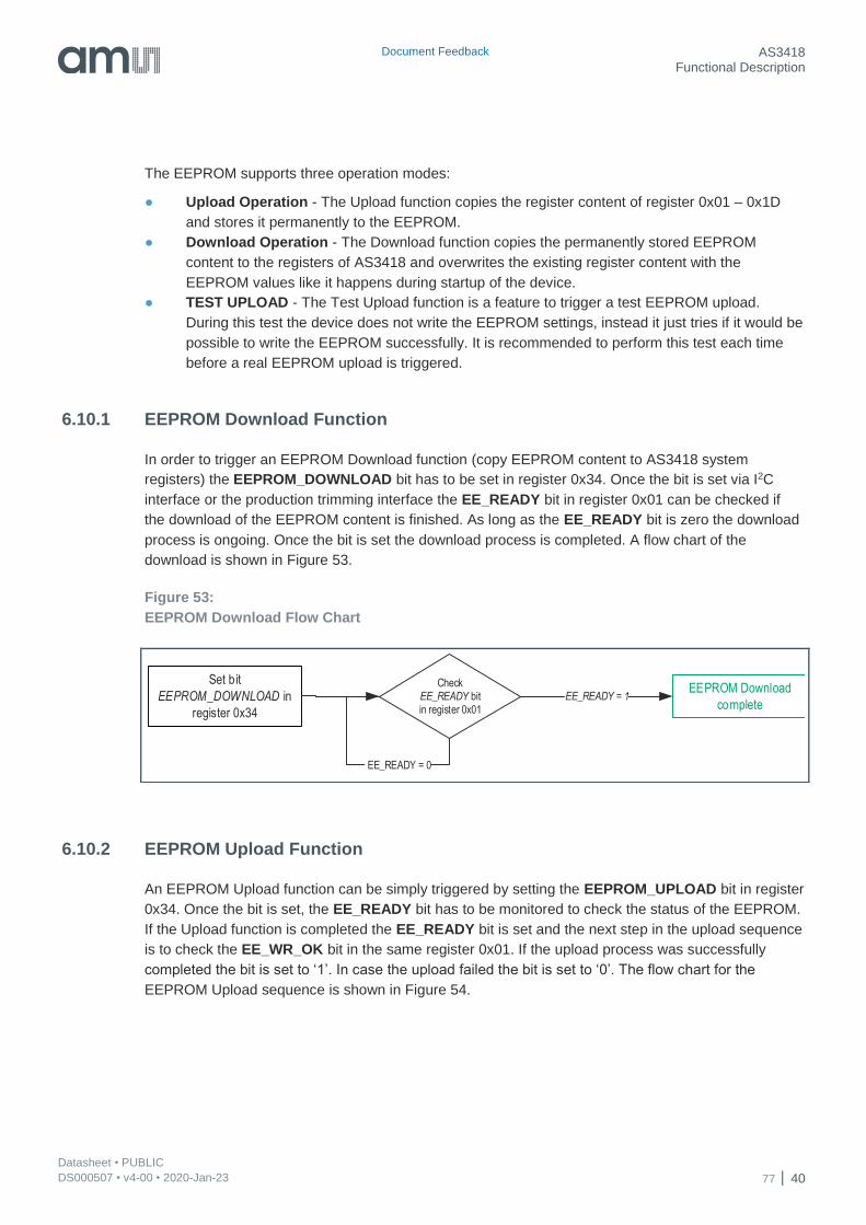
6.10.1 EEPROM Download Function
In order to trigger an EEPROM Download function (copy EEPROM content to AS3418 system
registers) the EEPROM_DOWNLOAD bit has to be set in register 0x34. Once the bit is set via I2C
interface or the production trimming interface the EE_READY bit in register 0x01 can be checked if
the download of the EEPROM content is finished. As long as the EE_READY bit is zero the download
process is ongoing. Once the bit is set the download process is completed. A flow chart of the
download is shown in Figure 53.
Figure 53:
EEPROM Download Flow Chart
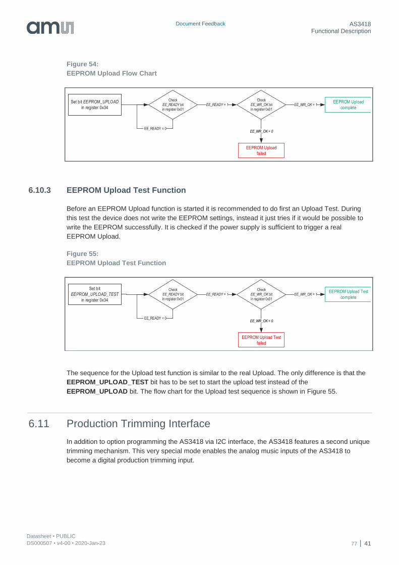
6.10.2 EEPROM Upload Function
An EEPROM Upload function can be simply triggered by setting the EEPROM_UPLOAD bit in register
0x34. Once the bit is set, the EE_READY bit has to be monitored to check the status of the EEPROM.
If the Upload function is completed the EE_READY bit is set and the next step in the upload sequence
is to check the EE_WR_OK bit in the same register 0x01. If the upload process was successfully
completed the bit is set to ‘1’. In case the upload failed the bit is set to ‘0’. The flow chart for the
EEPROM Upload sequence is shown in Figure 54.
Set bit
EEPROM_DOWNLOAD in
register 0x34
EEPROM Download
complete
Check EE_READY bitin register 0x01
EE_READY = 0
EE_READY = 1
Document Feedback AS3418 Functional Description
Datasheet • PUBLIC DS000507 • v4-00 • 2020-Jan-23 77 41
Figure 54:
EEPROM Upload Flow Chart
6.10.3 EEPROM Upload Test Function
Before an EEPROM Upload function is started it is recommended to do first an Upload Test. During
this test the device does not write the EEPROM settings, instead it just tries if it would be possible to
write the EEPROM successfully. It is checked if the power supply is sufficient to trigger a real
EEPROM Upload.
Figure 55:
EEPROM Upload Test Function
The sequence for the Upload test function is similar to the real Upload. The only difference is that the
EEPROM_UPLOAD_TEST bit has to be set to start the upload test instead of the
EEPROM_UPLOAD bit. The flow chart for the Upload test sequence is shown in Figure 55.
6.11 Production Trimming Interface
In addition to option programming the AS3418 via I2C interface, the AS3418 features a second unique
trimming mechanism. This very special mode enables the analog music inputs of the AS3418 to
become a digital production trimming input.
Set bit EEPROM_UPLOAD
in register 0x34
EEPROM Upload
complete
Check EE_READY bitin register 0x01
EE_READY = 0
EE_READY = 1Check
EE_WR_OK bitin register 0x01
EE_WR_OK = 1
EEPROM Upload
failed
EE_WR_OK = 0
Set bit
EEPROM_UPLOAD_TEST
in register 0x34
EEPROM Upload Test
complete
Check EE_READY bitin register 0x01
EE_READY = 0
EE_READY = 1Check
EE_WR_OK bitin register 0x01
EE_WR_OK = 1
EEPROM Upload Test
failed
EE_WR_OK = 0
Document Feedback AS3418 Functional Description
Datasheet • PUBLIC DS000507 • v4-00 • 2020-Jan-23 77 42
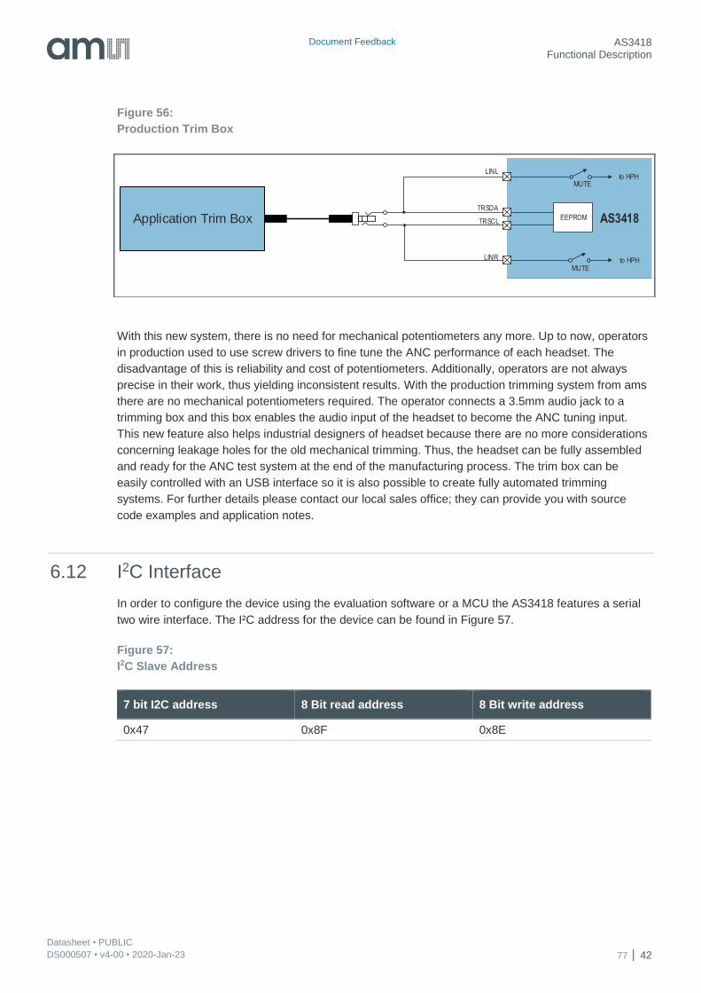
Figure 56:
Production Trim Box
With this new system, there is no need for mechanical potentiometers any more. Up to now, operators
in production used to use screw drivers to fine tune the ANC performance of each headset. The
disadvantage of this is reliability and cost of potentiometers. Additionally, operators are not always
precise in their work, thus yielding inconsistent results. With the production trimming system from ams
there are no mechanical potentiometers required. The operator connects a 3.5mm audio jack to a
trimming box and this box enables the audio input of the headset to become the ANC tuning input.
This new feature also helps industrial designers of headset because there are no more considerations
concerning leakage holes for the old mechanical trimming. Thus, the headset can be fully assembled
and ready for the ANC test system at the end of the manufacturing process. The trim box can be
easily controlled with an USB interface so it is also possible to create fully automated trimming
systems. For further details please contact our local sales office; they can provide you with source
code examples and application notes.
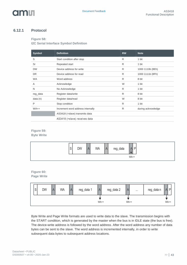
6.12 I2C Interface
In order to configure the device using the evaluation software or a MCU the AS3418 features a serial
two wire interface. The I²C address for the device can be found in Figure 57.
Figure 57:
I2C Slave Address
7 bit I2C address 8 Bit read address 8 Bit write address
0x47 0x8F 0x8E
LINR
TRSCL
MUTE
MUTE
TRSDA
EEPROM
to HPH
to HPH
Application Trim Box AS3418
LINL
Document Feedback AS3418 Functional Description
Datasheet • PUBLIC DS000507 • v4-00 • 2020-Jan-23 77 43
6.12.1 Protocol
Figure 58:
I2C Serial Interface Symbol Definition
Symbol Definition RW Note
S Start condition after stop R 1 bit
Sr Repeated start R 1 bit
DW Device address for write R 1000 1110b (8Eh)
DR Device address for read R 1000 1111b (8Fh)
WA Word address R 8 bit
A Acknowledge W 1 bit
N No Acknowledge R 1 bit
reg_data Register data/write R 8 bit
data (n) Register data/read W 8 bit
P Stop condition R 1 bit
WA++ Increment word address internally R during acknowledge
AS3418 (=slave) transmits data
AS3418 (=slave) receives data
Figure 59:
Byte Write
Figure 60:
Page Write
Byte Write and Page Write formats are used to write data to the slave. The transmission begins with
the START condition, which is generated by the master when the bus is in IDLE state (the bus is free).
The device-write address is followed by the word address. After the word address any number of data
bytes can be sent to the slave. The word address is incremented internally, in order to write
subsequent data bytes to subsequent address locations.
ADWS WA A reg_data P
WA++
A
ADWS WA A reg_data 1 A reg_data 2 A ... reg_data n
WA++ WA++ WA++
PA
Document Feedback AS3418 Functional Description
Datasheet • PUBLIC DS000507 • v4-00 • 2020-Jan-23 77 44
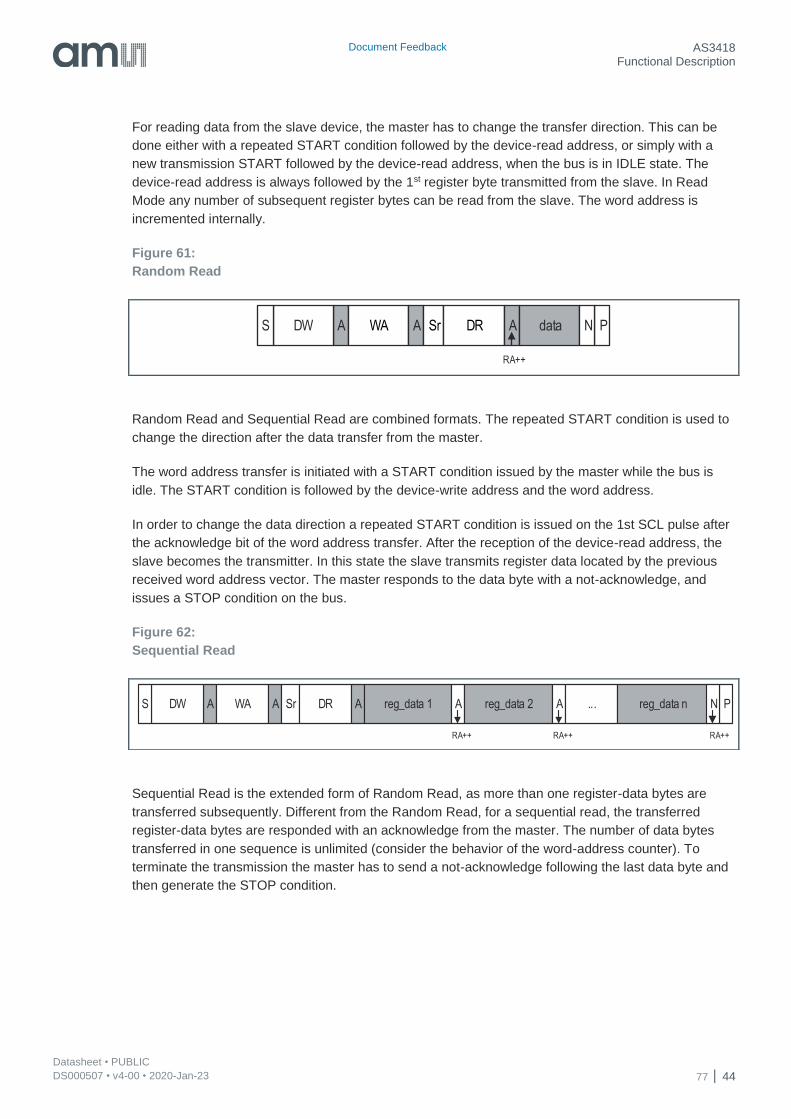
For reading data from the slave device, the master has to change the transfer direction. This can be
done either with a repeated START condition followed by the device-read address, or simply with a
new transmission START followed by the device-read address, when the bus is in IDLE state. The
device-read address is always followed by the 1st register byte transmitted from the slave. In Read
Mode any number of subsequent register bytes can be read from the slave. The word address is
incremented internally.
Figure 61:
Random Read
Random Read and Sequential Read are combined formats. The repeated START condition is used to
change the direction after the data transfer from the master.
The word address transfer is initiated with a START condition issued by the master while the bus is
idle. The START condition is followed by the device-write address and the word address.
In order to change the data direction a repeated START condition is issued on the 1st SCL pulse after
the acknowledge bit of the word address transfer. After the reception of the device-read address, the
slave becomes the transmitter. In this state the slave transmits register data located by the previous
received word address vector. The master responds to the data byte with a not-acknowledge, and
issues a STOP condition on the bus.
Figure 62:
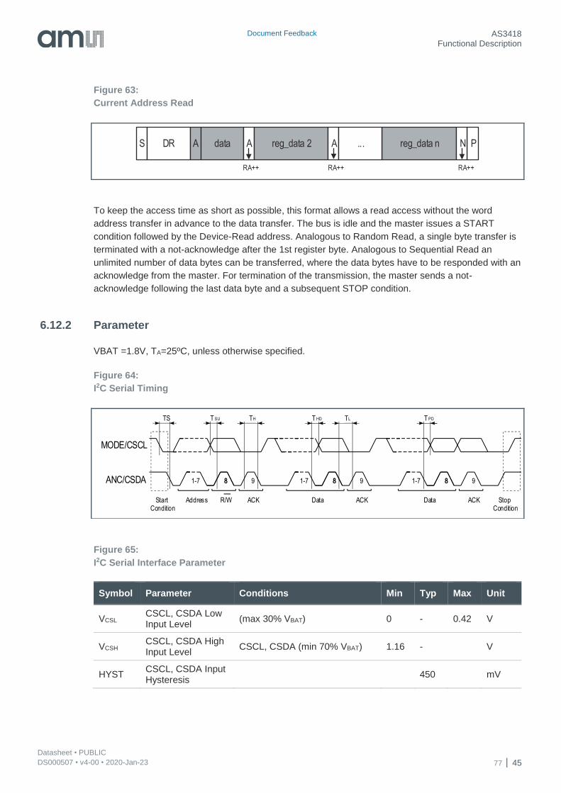
Sequential Read
Sequential Read is the extended form of Random Read, as more than one register-data bytes are
transferred subsequently. Different from the Random Read, for a sequential read, the transferred
register-data bytes are responded with an acknowledge from the master. The number of data bytes
transferred in one sequence is unlimited (consider the behavior of the word-address counter). To
terminate the transmission the master has to send a not-acknowledge following the last data byte and
then generate the STOP condition.
ADWS WA A Sr PDR A data N
RA++
ADWS WA A Sr DR A reg_data 1 A reg_data 2 A ... reg_data n
RA++ RA++ RA++
PN
Document Feedback AS3418 Functional Description
Datasheet • PUBLIC DS000507 • v4-00 • 2020-Jan-23 77 45
Figure 63:
Current Address Read
To keep the access time as short as possible, this format allows a read access without the word
address transfer in advance to the data transfer. The bus is idle and the master issues a START
condition followed by the Device-Read address. Analogous to Random Read, a single byte transfer is
terminated with a not-acknowledge after the 1st register byte. Analogous to Sequential Read an
unlimited number of data bytes can be transferred, where the data bytes have to be responded with an
acknowledge from the master. For termination of the transmission, the master sends a not-
acknowledge following the last data byte and a subsequent STOP condition.
6.12.2 Parameter
VBAT =1.8V, TA=25ºC, unless otherwise specified.
Figure 64:
I2C Serial Timing
Figure 65:
I2C Serial Interface Parameter
Symbol Parameter Conditions Min Typ Max Unit
VCSL CSCL, CSDA Low Input Level
(max 30% VBAT) 0 - 0.42 V
VCSH CSCL, CSDA High Input Level
CSCL, CSDA (min 70% VBAT) 1.16 - V
HYST CSCL, CSDA Input Hysteresis
450 mV
reg_data nS DR A data A reg_data 2 A ...
RA++ RA++ RA++
PN
81-7ANC/CSDA
MODE/CSCL
8 9 81-7 8 9 81-7 8 9
StartCondition
Address R/W ACK Data ACK Data ACK StopCondition
TS T SU TH TLT HD T PD
Document Feedback AS3418 Functional Description
Datasheet • PUBLIC DS000507 • v4-00 • 2020-Jan-23 77 46
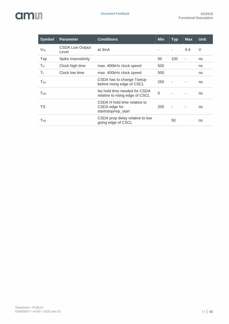
Symbol Parameter Conditions Min Typ Max Unit
VOL CSDA Low Output Level
at 3mA - - 0.4 V
Tsp Spike insensitivity 50 100 - ns
TH Clock high time max. 400kHz clock speed 500 ns
TL Clock low time max. 400kHz clock speed 500 ns
TSU CSDA has to change Tsetup before rising edge of CSCL
250 - - ns
THD No hold time needed for CSDA relative to rising edge of CSCL
0 - - ns
TS CSDA H hold time relative to CSDA edge for start/stop/rep_start
200 - - ns
TPD CSDA prop delay relative to low going edge of CSCL
50 ns
Document Feedback AS3418 Register Description
Datasheet • PUBLIC DS000507 • v4-00 • 2020-Jan-23 77 47
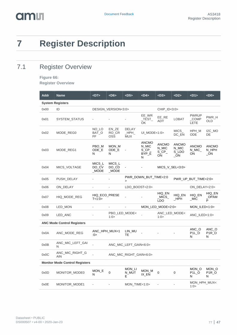
7 Register Description
7.1 Register Overview
Figure 66:
Register Overview
Addr Name <D7> <D6> <D5> <D4> <D3> <D2> <D1> <D0>
System Registers
0x00 ID DESIGN_VERSION<3:0> CHIP_ID<3:0>
0x01 SYSTEM_STATUS - - - EE_WR_TEST_OK
EE_READY
LOBAT PWRUP_COMPLETE
PWR_HOLD
0x02 MODE_REG0 NO_LOBAT_OFF
EN_ZERO_CROSS
DELAY_HPH_MUX
UI_MODE<1:0> MICS_DC_EN
HPH_MODE
I2C_MODE
0x03 MODE_REG1 PBO_MODE_EN
MON_MODE_EN
-
ANCMON_MICS_CP_BYP_EN
ANCMON_MICS_CP_ON
ANCMON_MICS_LDO_ON
ANCMON_MIC_ON
ANCMON_HPH_ON
0x04 MICS_VOLTAGE MICS_LDO_CV_MODE
MICS_LDO_CD_MODE
- - MICS_V_SEL<3:0>
0x05 PUSH_DELAY - - PWR_DOWN_BUT_TIME<2:0>
PWR_UP_BUT_TIME<2:0>
0x06 ON_DELAY - - LDO_BOOST<2:0> ON_DELAY<2:0>
0x07 HIQ_MODE_REG HIQ_ECO_PRESET<1:0>
- - HIQ_EN_MICS_LDO
HIQ_EN_HPH
HIQ_EN_MIC
HIQ_EN_OPAMP
0x08 LED_MON - - - MON_LED_MODE<2:0> MON_ILED<1:0>
0x09 LED_ANC - PBO_LED_MODE<1:0>
- ANC_LED_MODE<1:0>
ANC_ILED<1:0>
ANC Mode Control Registers
0x0A ANC_MODE_REG ANC_HPH_MUX<1:0>
LIN_MUTE
- - - ANC_OP1L_ON
ANC_OP1R_ON
0x0B ANC_MIC_LEFT_GAIN
- ANC_MIC_LEFT_GAIN<6:0>
0x0C ANC_MIC_RIGHT_GAIN
- ANC_MIC_RIGHT_GAIN<6:0>
Monitor Mode Control Registers
0x0D MONITOR_MODE0 MON_EN
0 MON_LIN_MUTE
MON_MIX_EN
0 0 MON_OP1L_ON
MON_OP1R_ON
0x0E MONITOR_MODE1 - - MON_TIME<1:0> - - MON_HPH_MUX<1:0>
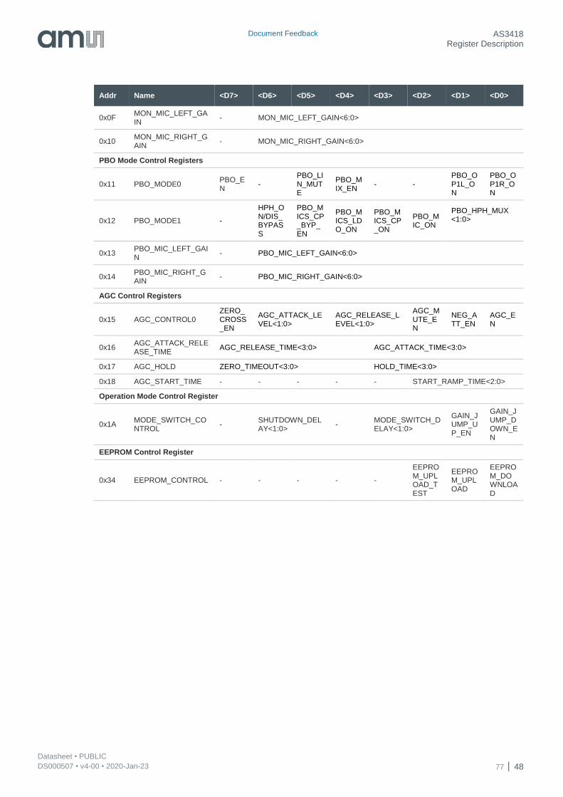
Document Feedback AS3418 Register Description
Datasheet • PUBLIC DS000507 • v4-00 • 2020-Jan-23 77 48
Addr Name <D7> <D6> <D5> <D4> <D3> <D2> <D1> <D0>
0x0F MON_MIC_LEFT_GAIN
- MON_MIC_LEFT_GAIN<6:0>
0x10 MON_MIC_RIGHT_GAIN
- MON_MIC_RIGHT_GAIN<6:0>
PBO Mode Control Registers
0x11 PBO_MODE0 PBO_EN
- PBO_LIN_MUTE
PBO_MIX_EN
- - PBO_OP1L_ON
PBO_OP1R_ON
0x12 PBO_MODE1 -
HPH_ON/DIS_BYPASS
PBO_MICS_CP_BYP_EN
PBO_MICS_LDO_ON
PBO_MICS_CP_ON
PBO_MIC_ON
PBO_HPH_MUX <1:0>
0x13 PBO_MIC_LEFT_GAIN
- PBO_MIC_LEFT_GAIN<6:0>
0x14 PBO_MIC_RIGHT_GAIN
- PBO_MIC_RIGHT_GAIN<6:0>
AGC Control Registers
0x15 AGC_CONTROL0 ZERO_CROSS_EN
AGC_ATTACK_LEVEL<1:0>
AGC_RELEASE_LEVEL<1:0>
AGC_MUTE_EN
NEG_ATT_EN
AGC_EN
0x16 AGC_ATTACK_RELEASE_TIME
AGC_RELEASE_TIME<3:0> AGC_ATTACK_TIME<3:0>
0x17 AGC_HOLD ZERO_TIMEOUT<3:0> HOLD_TIME<3:0>
0x18 AGC_START_TIME - - - - - START_RAMP_TIME<2:0>
Operation Mode Control Register
0x1A MODE_SWITCH_CONTROL
- SHUTDOWN_DELAY<1:0>
- MODE_SWITCH_DELAY<1:0>
GAIN_JUMP_UP_EN
GAIN_JUMP_DOWN_EN
EEPROM Control Register
0x34 EEPROM_CONTROL - - - - -
EEPROM_UPLOAD_TEST
EEPROM_UPLOAD
EEPROM_DOWNLOAD
Document Feedback AS3418 Register Description
Datasheet • PUBLIC DS000507 • v4-00 • 2020-Jan-23 77 49
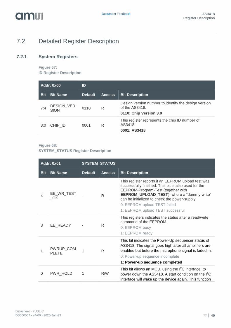
7.2 Detailed Register Description
7.2.1 System Registers
Figure 67:
ID Register Description
Addr: 0x00 ID
Bit Bit Name Default Access Bit Description
7:4 DESIGN_VERSION
0110 R
Design version number to identify the design version of the AS3418.
0110: Chip Version 3.0
3:0 CHIP_ID 0001 R
This register represents the chip ID number of AS3418.
0001: AS3418
Figure 68:
SYSTEM_STATUS Register Description
Addr: 0x01 SYSTEM_STATUS
Bit Bit Name Default Access Bit Description
4 EE_WR_TEST_OK
- R
This register reports if an EEPROM upload test was successfully finished. This bit is also used for the EEPROM-Program-Test (together with EEPROM_UPLOAD_TEST), where a “dummy-write” can be initialized to check the power-supply
0: EEPROM upload TEST failed
1: EEPROM upload TEST successful
3 EE_READY - R
This registers indicates the status after a read/write command of the EEPROM.
0: EEPROM busy
1: EEPROM ready
1 PWRUP_COMPLETE
1 R
This bit indicates the Power-Up sequencer status of
AS3418. The signal goes high after all amplifiers are
enabled but before the microphone signal is faded in.
0: Power-up sequence incomplete
1: Power-up sequence completed
0 PWR_HOLD 1 R/W This bit allows an MCU, using the I2C interface, to
power down the AS3418. A start condition on the I2C
interface will wake up the device again. This function
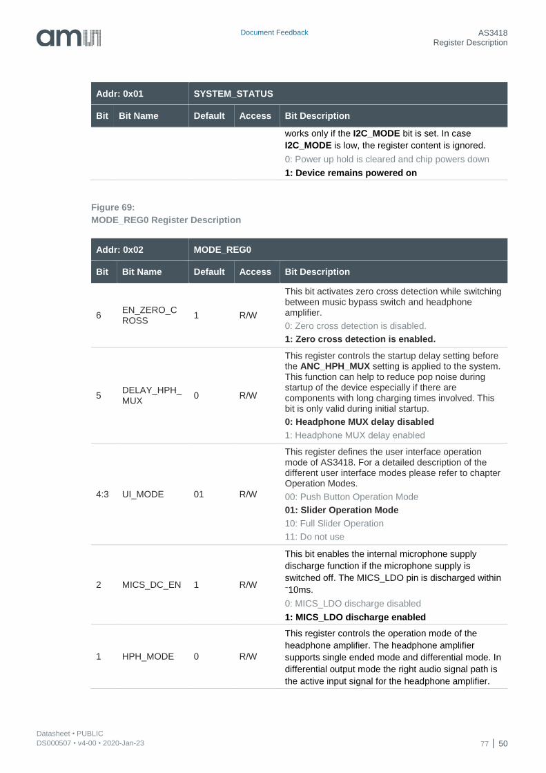
Document Feedback AS3418 Register Description
Datasheet • PUBLIC DS000507 • v4-00 • 2020-Jan-23 77 50
Addr: 0x01 SYSTEM_STATUS
Bit Bit Name Default Access Bit Description
works only if the I2C_MODE bit is set. In case
I2C_MODE is low, the register content is ignored.
0: Power up hold is cleared and chip powers down
1: Device remains powered on
Figure 69:
MODE_REG0 Register Description
Addr: 0x02 MODE_REG0
Bit Bit Name Default Access Bit Description
6 EN_ZERO_CROSS
1 R/W
This bit activates zero cross detection while switching between music bypass switch and headphone amplifier.
0: Zero cross detection is disabled.
1: Zero cross detection is enabled.
5 DELAY_HPH_MUX
0 R/W
This register controls the startup delay setting before the ANC_HPH_MUX setting is applied to the system. This function can help to reduce pop noise during startup of the device especially if there are components with long charging times involved. This bit is only valid during initial startup.
0: Headphone MUX delay disabled
1: Headphone MUX delay enabled
4:3 UI_MODE 01 R/W
This register defines the user interface operation mode of AS3418. For a detailed description of the different user interface modes please refer to chapter Operation Modes.
00: Push Button Operation Mode
01: Slider Operation Mode
10: Full Slider Operation
11: Do not use
2 MICS_DC_EN 1 R/W
This bit enables the internal microphone supply
discharge function if the microphone supply is
switched off. The MICS_LDO pin is discharged within ~10ms.
0: MICS_LDO discharge disabled
1: MICS_LDO discharge enabled
1 HPH_MODE 0 R/W
This register controls the operation mode of the
headphone amplifier. The headphone amplifier
supports single ended mode and differential mode. In
differential output mode the right audio signal path is
the active input signal for the headphone amplifier.
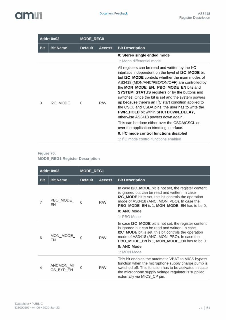
Document Feedback AS3418 Register Description
Datasheet • PUBLIC DS000507 • v4-00 • 2020-Jan-23 77 51
Addr: 0x02 MODE_REG0
Bit Bit Name Default Access Bit Description
0: Stereo single ended mode
1: Mono differential mode
0 I2C_MODE 0 R/W
All registers can be read and written by the I2C
interface independent on the level of I2C_MODE bit
but I2C_MODE controls whether the main modes of
AS3418 (MON/ANC/PBO/ON/OFF) are controlled by
the MON_MODE_EN, PBO_MODE_EN bits and
SYSTEM_STATUS registers or by the buttons and
switches. Once the bit is set and the system powers
up because there’s an I2C start condition applied to
the CSCL and CSDA pins, the user has to write the
PWR_HOLD bit within SHUTDOWN_DELAY,
otherwise AS3418 powers down again.
This can be done either over the CSDA/CSCL or
over the application trimming interface.
0: I2C mode control functions disabled
1: I2C mode control functions enabled
Figure 70:
MODE_REG1 Register Description
Addr: 0x03 MODE_REG1
Bit Bit Name Default Access Bit Description
7 PBO_MODE_EN
0 R/W
In case I2C_MODE bit is not set, the register content is ignored but can be read and written. In case I2C_MODE bit is set, this bit controls the operation mode of AS3418 (ANC, MON, PBO). In case the PBO_MODE_EN is 1, MON_MODE_EN has to be 0.
0: ANC Mode
1: PBO Mode
6 MON_MODE_EN
0 R/W
In case I2C_MODE bit is not set, the register content is ignored but can be read and written. In case I2C_MODE bit is set, this bit controls the operation mode of AS3418 (ANC, MON, PBO). In case the PBO_MODE_EN is 1, MON_MODE_EN has to be 0.
0: ANC Mode
1: MON Mode
4 ANCMON_MICS_BYP_EN
0 R/W
This bit enables the automatic VBAT to MICS bypass function when the microphone supply charge pump is switched off. This function has to be activated in case the microphone supply voltage regulator is supplied externally via MICS_CP pin.
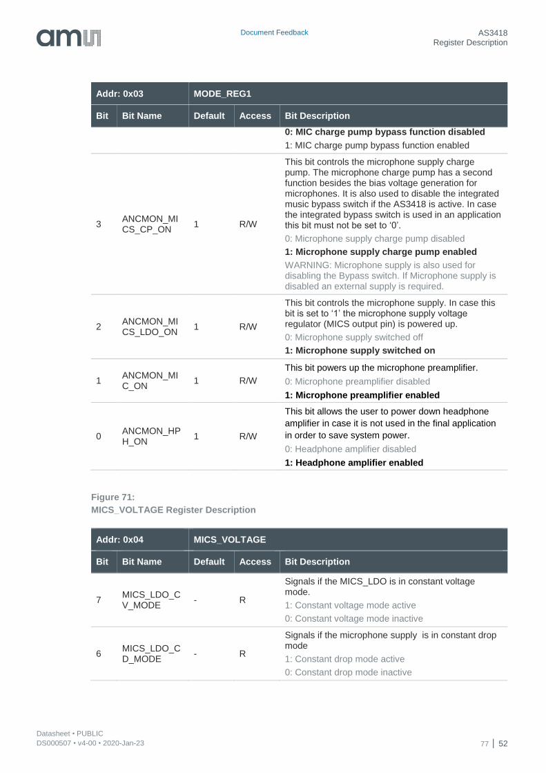
Document Feedback AS3418 Register Description
Datasheet • PUBLIC DS000507 • v4-00 • 2020-Jan-23 77 52
Addr: 0x03 MODE_REG1
Bit Bit Name Default Access Bit Description
0: MIC charge pump bypass function disabled
1: MIC charge pump bypass function enabled
3 ANCMON_MICS_CP_ON
1 R/W
This bit controls the microphone supply charge pump. The microphone charge pump has a second function besides the bias voltage generation for microphones. It is also used to disable the integrated music bypass switch if the AS3418 is active. In case the integrated bypass switch is used in an application this bit must not be set to ‘0’.
0: Microphone supply charge pump disabled
1: Microphone supply charge pump enabled
WARNING: Microphone supply is also used for disabling the Bypass switch. If Microphone supply is disabled an external supply is required.
2 ANCMON_MICS_LDO_ON
1 R/W
This bit controls the microphone supply. In case this bit is set to ‘1’ the microphone supply voltage regulator (MICS output pin) is powered up.
0: Microphone supply switched off
1: Microphone supply switched on
1 ANCMON_MIC_ON
1 R/W
This bit powers up the microphone preamplifier.
0: Microphone preamplifier disabled
1: Microphone preamplifier enabled
0 ANCMON_HPH_ON
1 R/W
This bit allows the user to power down headphone
amplifier in case it is not used in the final application
in order to save system power.
0: Headphone amplifier disabled
1: Headphone amplifier enabled
Figure 71:
MICS_VOLTAGE Register Description
Addr: 0x04 MICS_VOLTAGE
Bit Bit Name Default Access Bit Description
7 MICS_LDO_CV_MODE
- R
Signals if the MICS_LDO is in constant voltage mode.
1: Constant voltage mode active
0: Constant voltage mode inactive
6 MICS_LDO_CD_MODE
- R
Signals if the microphone supply is in constant drop mode
1: Constant drop mode active
0: Constant drop mode inactive
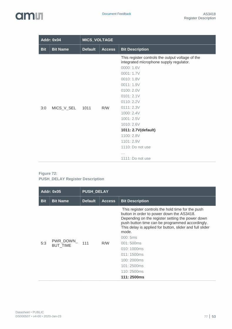
Document Feedback AS3418 Register Description
Datasheet • PUBLIC DS000507 • v4-00 • 2020-Jan-23 77 53
Addr: 0x04 MICS_VOLTAGE
Bit Bit Name Default Access Bit Description
3:0 MICS_V_SEL 1011 R/W
This register controls the output voltage of the integrated microphone supply regulator.
0000: 1.6V
0001: 1.7V
0010: 1.8V
0011: 1.9V
0100: 2.0V
0101: 2.1V
0110: 2.2V
0111: 2.3V
1000: 2.4V
1001: 2.5V
1010: 2.6V
1011: 2.7V(default)
1100: 2.8V
1101: 2.9V
1110: Do not use
…
1111: Do not use
Figure 72:
PUSH_DELAY Register Description
Addr: 0x05 PUSH_DELAY
Bit Bit Name Default Access Bit Description
5:3 PWR_DOWN_BUT_TIME
111 R/W
This register controls the hold time for the push button in order to power down the AS3418. Depending on the register setting the power down push button time can be programmed accordingly. This delay is applied for button, slider and full slider mode.
000: 5ms
001: 500ms
010: 1000ms
011: 1500ms
100: 2000ms
101: 2500ms
110: 2500ms
111: 2500ms
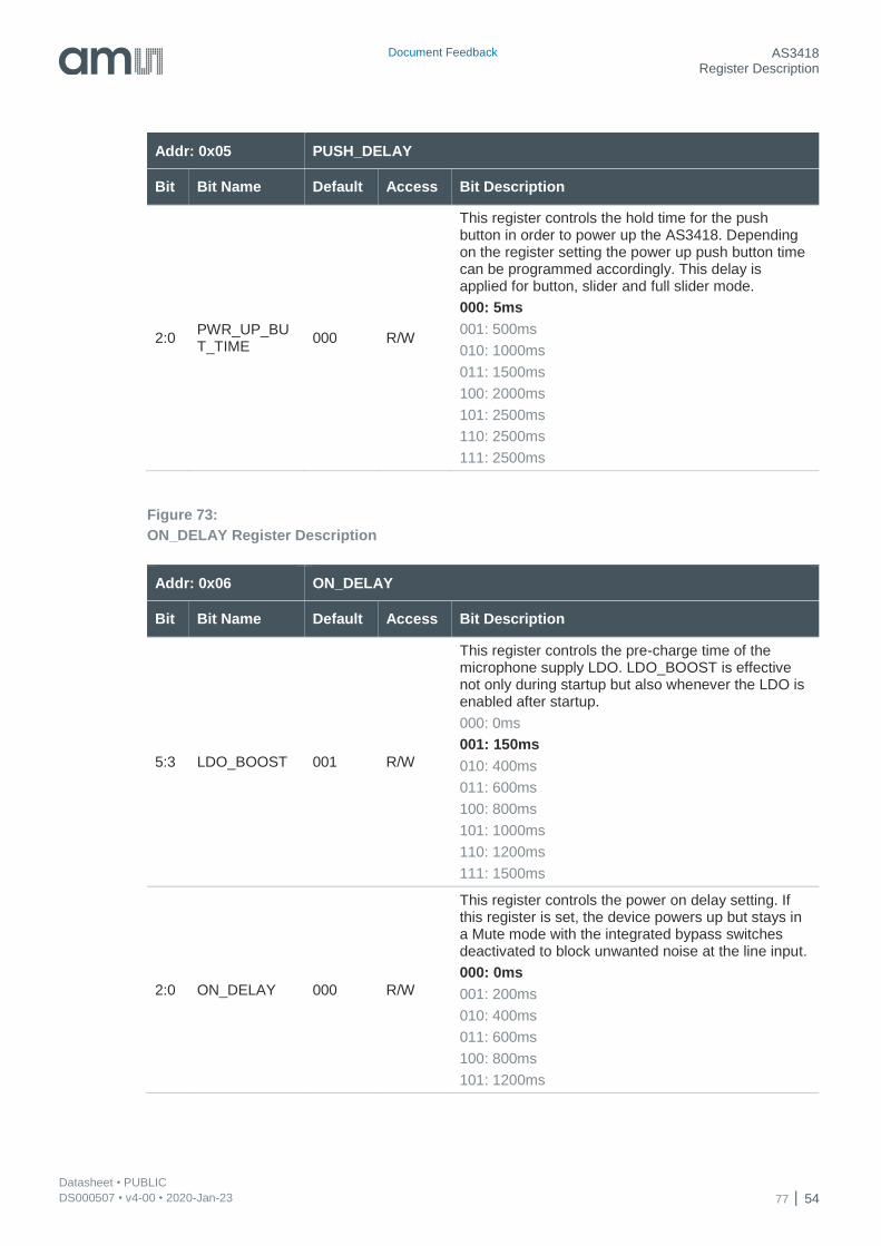
Document Feedback AS3418 Register Description
Datasheet • PUBLIC DS000507 • v4-00 • 2020-Jan-23 77 54
Addr: 0x05 PUSH_DELAY
Bit Bit Name Default Access Bit Description
2:0 PWR_UP_BUT_TIME
000 R/W
This register controls the hold time for the push button in order to power up the AS3418. Depending on the register setting the power up push button time can be programmed accordingly. This delay is applied for button, slider and full slider mode.
000: 5ms
001: 500ms
010: 1000ms
011: 1500ms
100: 2000ms
101: 2500ms
110: 2500ms
111: 2500ms
Figure 73:
ON_DELAY Register Description
Addr: 0x06 ON_DELAY
Bit Bit Name Default Access Bit Description
5:3 LDO_BOOST 001 R/W
This register controls the pre-charge time of the microphone supply LDO. LDO_BOOST is effective not only during startup but also whenever the LDO is enabled after startup.
000: 0ms
001: 150ms
010: 400ms
011: 600ms
100: 800ms
101: 1000ms
110: 1200ms
111: 1500ms
2:0 ON_DELAY 000 R/W
This register controls the power on delay setting. If this register is set, the device powers up but stays in a Mute mode with the integrated bypass switches deactivated to block unwanted noise at the line input.
000: 0ms
001: 200ms
010: 400ms
011: 600ms
100: 800ms
101: 1200ms
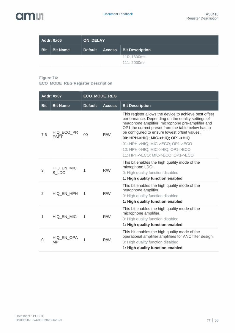
Document Feedback AS3418 Register Description
Datasheet • PUBLIC DS000507 • v4-00 • 2020-Jan-23 77 55
Addr: 0x06 ON_DELAY
Bit Bit Name Default Access Bit Description
110: 1600ms
111: 2000ms
Figure 74:
ECO_MODE_REG Register Description
Addr: 0x07 ECO_MODE_REG
Bit Bit Name Default Access Bit Description
7:6 HIQ_ECO_PRESET
00 R/W
This register allows the device to achieve best offset performance. Depending on the quality settings of headphone amplifier, microphone pre-amplifier and OP1 the correct preset from the table below has to be configured to ensure lowest offset values.
00: HPH->HIQ; MIC->HIQ; OP1->HIQ
01: HPH->HIQ; MIC->ECO; OP1->ECO
10: HPH->HIQ; MIC->HIQ; OP1->ECO
11: HPH->ECO; MIC->ECO; OP1->ECO
3 HIQ_EN_MICS_LDO
1 R/W
This bit enables the high quality mode of the microphone LDO.
0: High quality function disabled
1: High quality function enabled
2 HIQ_EN_HPH 1 R/W
This bit enables the high quality mode of the headphone amplifier.
0: High quality function disabled
1: High quality function enabled
1 HIQ_EN_MIC 1 R/W
This bit enables the high quality mode of the microphone amplifier.
0: High quality function disabled
1: High quality function enabled
0 HIQ_EN_OPAMP
1 R/W
This bit enables the high quality mode of the operational amplifier amplifiers for ANC filter design.
0: High quality function disabled
1: High quality function enabled
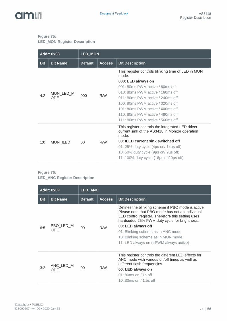
Document Feedback AS3418 Register Description
Datasheet • PUBLIC DS000507 • v4-00 • 2020-Jan-23 77 56
Figure 75:
LED_MON Register Description
Addr: 0x08 LED_MON
Bit Bit Name Default Access Bit Description
4:2 MON_LED_MODE
000 R/W
This register controls blinking time of LED in MON mode.
000: LED always on
001: 80ms PWM active / 80ms off
010: 80ms PWM active / 160ms off
011: 80ms PWM active / 240ms off
100: 80ms PWM active / 320ms off
101: 80ms PWM active / 400ms off
110: 80ms PWM active / 480ms off
111: 80ms PWM active / 560ms off
1:0 MON_ILED 00 R/W
This register controls the integrated LED driver current sink of the AS3418 in Monitor operation mode.
00: ILED current sink switched off
01: 25% duty cycle (4µs on/ 14µs off)
10: 50% duty cycle (9µs on/ 9µs off)
11: 100% duty cycle (18µs on/ 0µs off)
Figure 76:
LED_ANC Register Description
Addr: 0x09 LED_ANC
Bit Bit Name Default Access Bit Description
6:5 PBO_LED_MODE
00 R/W
Defines the blinking scheme if PBO mode is active. Please note that PBO mode has not an individual LED control register. Therefore this setting uses hardcoded 25% PWM duty cycle for brightness.
00: LED always off
01: Blinking scheme as in ANC mode
10: Blinking scheme as in MON mode
11: LED always on (=PWM always active)
3:2 ANC_LED_MODE
00 R/W
This register controls the different LED effects for ANC mode with various on/off times as well as different flash frequencies.
00: LED always on
01: 80ms on / 1s off
10: 80ms on / 1.5s off
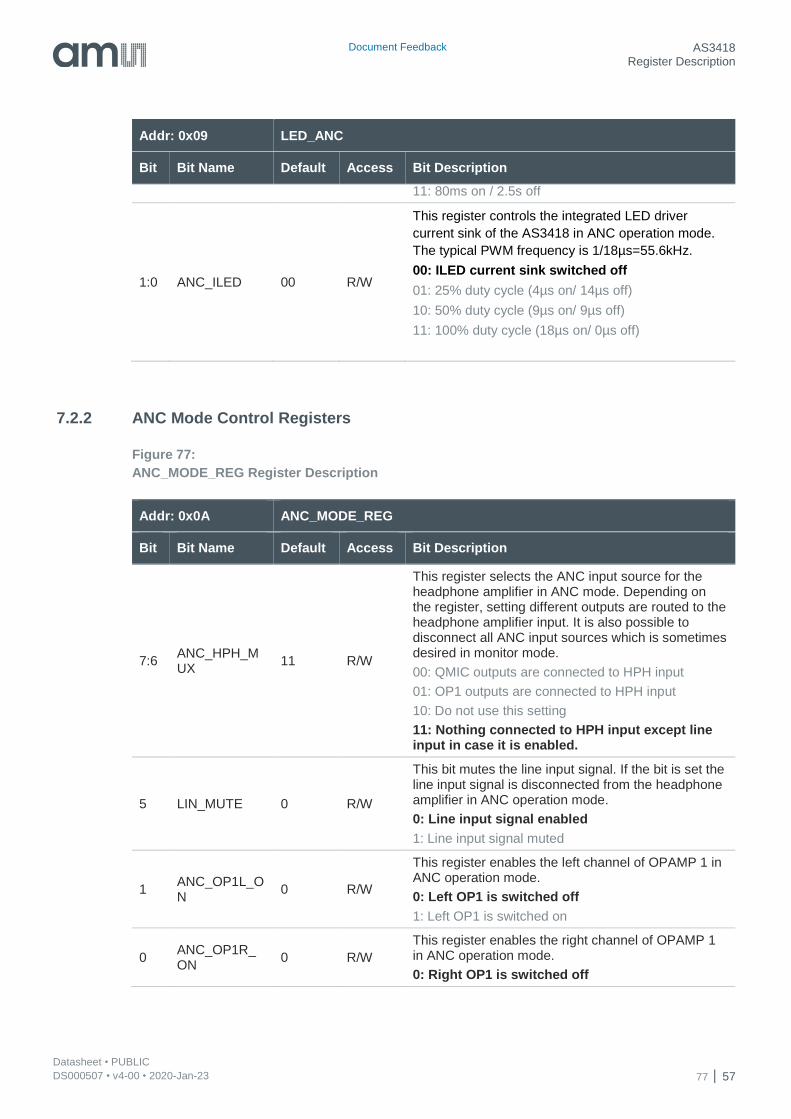
Document Feedback AS3418 Register Description
Datasheet • PUBLIC DS000507 • v4-00 • 2020-Jan-23 77 57
Addr: 0x09 LED_ANC
Bit Bit Name Default Access Bit Description
11: 80ms on / 2.5s off
1:0 ANC_ILED 00 R/W
This register controls the integrated LED driver
current sink of the AS3418 in ANC operation mode.
The typical PWM frequency is 1/18µs=55.6kHz.
00: ILED current sink switched off
01: 25% duty cycle (4µs on/ 14µs off)
10: 50% duty cycle (9µs on/ 9µs off)
11: 100% duty cycle (18µs on/ 0µs off)
7.2.2 ANC Mode Control Registers
Figure 77:
ANC_MODE_REG Register Description
Addr: 0x0A ANC_MODE_REG
Bit Bit Name Default Access Bit Description
7:6 ANC_HPH_MUX
11 R/W
This register selects the ANC input source for the headphone amplifier in ANC mode. Depending on the register, setting different outputs are routed to the headphone amplifier input. It is also possible to disconnect all ANC input sources which is sometimes desired in monitor mode.
00: QMIC outputs are connected to HPH input
01: OP1 outputs are connected to HPH input
10: Do not use this setting
11: Nothing connected to HPH input except line input in case it is enabled.
5 LIN_MUTE 0 R/W
This bit mutes the line input signal. If the bit is set the line input signal is disconnected from the headphone amplifier in ANC operation mode.
0: Line input signal enabled
1: Line input signal muted
1 ANC_OP1L_ON
0 R/W
This register enables the left channel of OPAMP 1 in ANC operation mode.
0: Left OP1 is switched off
1: Left OP1 is switched on
0 ANC_OP1R_ON
0 R/W
This register enables the right channel of OPAMP 1 in ANC operation mode.
0: Right OP1 is switched off
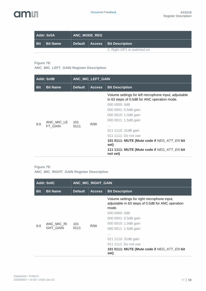
Document Feedback AS3418 Register Description
Datasheet • PUBLIC DS000507 • v4-00 • 2020-Jan-23 77 58
Addr: 0x0A ANC_MODE_REG
Bit Bit Name Default Access Bit Description
1: Right OP1 is switched on
Figure 78:
ANC_MIC_LEFT_GAIN Register Description
Addr: 0x0B ANC_MIC_LEFT_GAIN
Bit Bit Name Default Access Bit Description
6:0 ANC_MIC_LEFT_GAIN
101 0111
R/W
Volume settings for left microphone input, adjustable
in 63 steps of 0.5dB for ANC operation mode.
000 0000: 0dB
000 0001: 0.5dB gain
000 0010: 1.0dB gain
000 0011: 1.5dB gain
…
011 1110: 31dB gain
011 1111: Do not use
101 0111: MUTE (Mute code if NEG_ATT_EN bit set)
111 1111: MUTE (Mute code if NEG_ATT_EN bit not set)
Figure 79:
ANC_MIC_RIGHT_GAIN Register Description
Addr: 0x0C ANC_MIC_RIGHT_GAIN
Bit Bit Name Default Access Bit Description
6:0 ANC_MIC_RIGHT_GAIN
101 0111
R/W
Volume settings for right microphone input,
adjustable in 63 steps of 0.5dB for ANC operation
mode.
000 0000: 0dB
000 0001: 0.5dB gain
000 0010: 1.0dB gain
000 0011: 1.5dB gain
…
011 1110: 31dB gain
011 1111: Do not use
101 0111: MUTE (Mute code if NEG_ATT_EN bit set)
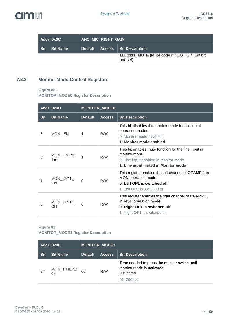
Document Feedback AS3418 Register Description
Datasheet • PUBLIC DS000507 • v4-00 • 2020-Jan-23 77 59
Addr: 0x0C ANC_MIC_RIGHT_GAIN
Bit Bit Name Default Access Bit Description
111 1111: MUTE (Mute code if NEG_ATT_EN bit not set)
7.2.3 Monitor Mode Control Registers
Figure 80:
MONITOR_MODE0 Register Description
Addr: 0x0D MONITOR_MODE0
Bit Bit Name Default Access Bit Description
7 MON_ EN 1 R/W
This bit disables the monitor mode function in all
operation modes.
0: Monitor mode disabled
1: Monitor mode enabled
5 MON_LIN_MUTE
1 R/W
This bit enables mute function for the line input in
monitor more.
0: Line input enabled in Monitor mode
1: Line input muted in Monitor mode
1 MON_OP1L_ON
0 R/W
This register enables the left channel of OPAMP 1 in
MON operation mode.
0: Left OP1 is switched off
1: Left OP1 is switched on
0 MON_OP1R_ON
0 R/W
This register enables the right channel of OPAMP 1
in MON operation mode.
0: Right OP1 is switched off
1: Right OP1 is switched on
Figure 81:
MONITOR_MODE1 Register Description
Addr: 0x0E MONITOR_MODE1
Bit Bit Name Default Access Bit Description
5:4 MON_TIME<1:0>
00 R/W
Time needed to press the monitor switch until
monitor mode is activated.
00: 25ms
01: 200ms
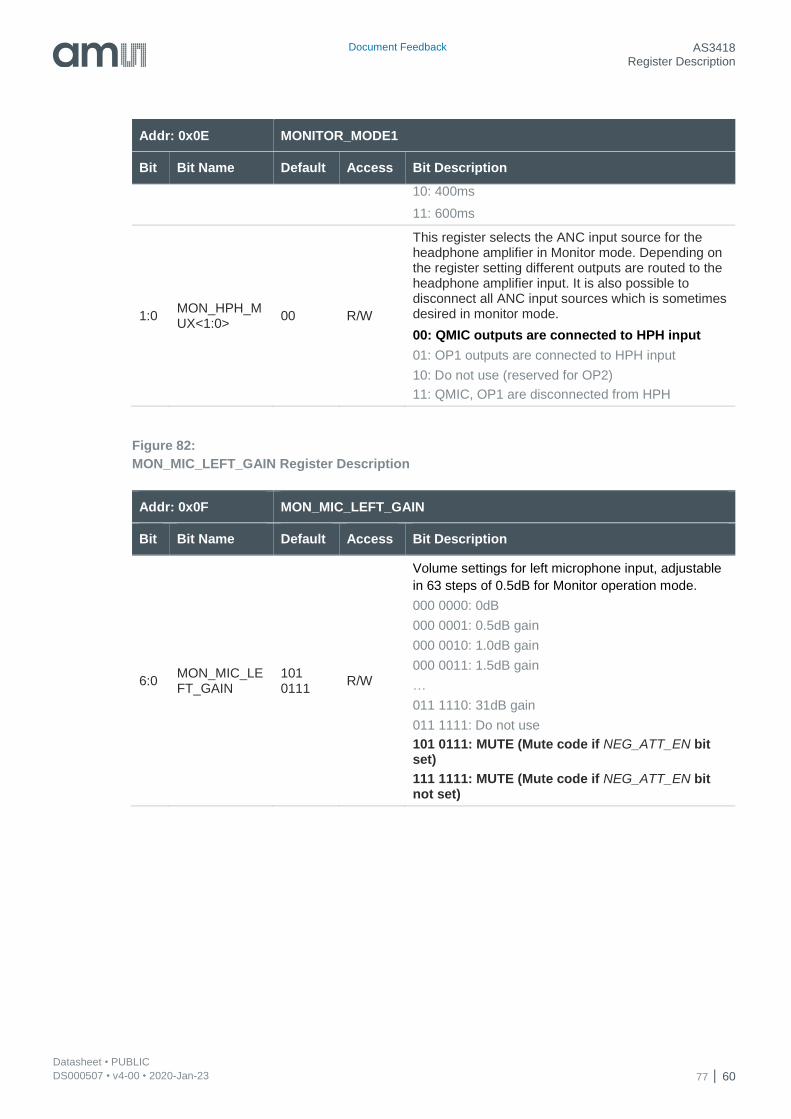
Document Feedback AS3418 Register Description
Datasheet • PUBLIC DS000507 • v4-00 • 2020-Jan-23 77 60
Addr: 0x0E MONITOR_MODE1
Bit Bit Name Default Access Bit Description
10: 400ms
11: 600ms
1:0 MON_HPH_MUX<1:0>
00 R/W
This register selects the ANC input source for the headphone amplifier in Monitor mode. Depending on the register setting different outputs are routed to the headphone amplifier input. It is also possible to disconnect all ANC input sources which is sometimes desired in monitor mode.
00: QMIC outputs are connected to HPH input
01: OP1 outputs are connected to HPH input
10: Do not use (reserved for OP2)
11: QMIC, OP1 are disconnected from HPH
Figure 82:
MON_MIC_LEFT_GAIN Register Description
Addr: 0x0F MON_MIC_LEFT_GAIN
Bit Bit Name Default Access Bit Description
6:0 MON_MIC_LEFT_GAIN
101 0111
R/W
Volume settings for left microphone input, adjustable
in 63 steps of 0.5dB for Monitor operation mode.
000 0000: 0dB
000 0001: 0.5dB gain
000 0010: 1.0dB gain
000 0011: 1.5dB gain
…
011 1110: 31dB gain
011 1111: Do not use
101 0111: MUTE (Mute code if NEG_ATT_EN bit set)
111 1111: MUTE (Mute code if NEG_ATT_EN bit not set)
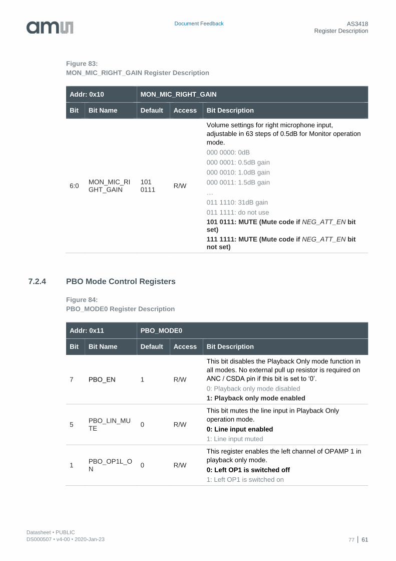
Document Feedback AS3418 Register Description
Datasheet • PUBLIC DS000507 • v4-00 • 2020-Jan-23 77 61
Figure 83:
MON_MIC_RIGHT_GAIN Register Description
Addr: 0x10 MON_MIC_RIGHT_GAIN
Bit Bit Name Default Access Bit Description
6:0 MON_MIC_RIGHT_GAIN
101 0111
R/W
Volume settings for right microphone input,
adjustable in 63 steps of 0.5dB for Monitor operation
mode.
000 0000: 0dB
000 0001: 0.5dB gain
000 0010: 1.0dB gain
000 0011: 1.5dB gain
…
011 1110: 31dB gain
011 1111: do not use
101 0111: MUTE (Mute code if NEG_ATT_EN bit set)
111 1111: MUTE (Mute code if NEG_ATT_EN bit not set)
7.2.4 PBO Mode Control Registers
Figure 84:
PBO_MODE0 Register Description
Addr: 0x11 PBO_MODE0
Bit Bit Name Default Access Bit Description
7 PBO_EN 1 R/W
This bit disables the Playback Only mode function in
all modes. No external pull up resistor is required on
ANC / CSDA pin if this bit is set to ‘0’.
0: Playback only mode disabled
1: Playback only mode enabled
5 PBO_LIN_MUTE
0 R/W
This bit mutes the line input in Playback Only
operation mode.
0: Line input enabled
1: Line input muted
1 PBO_OP1L_ON
0 R/W
This register enables the left channel of OPAMP 1 in
playback only mode.
0: Left OP1 is switched off
1: Left OP1 is switched on
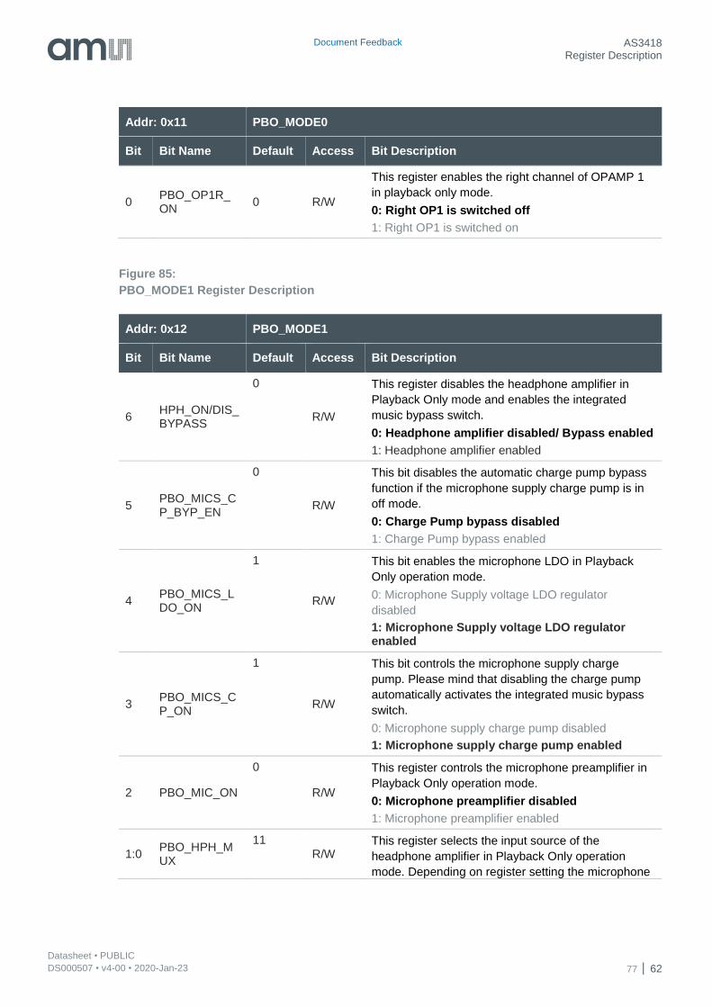
Document Feedback AS3418 Register Description
Datasheet • PUBLIC DS000507 • v4-00 • 2020-Jan-23 77 62
Addr: 0x11 PBO_MODE0
Bit Bit Name Default Access Bit Description
0 PBO_OP1R_ON
0 R/W
This register enables the right channel of OPAMP 1
in playback only mode.
0: Right OP1 is switched off
1: Right OP1 is switched on
Figure 85:
PBO_MODE1 Register Description
Addr: 0x12 PBO_MODE1
Bit Bit Name Default Access Bit Description
6 HPH_ON/DIS_BYPASS
0
R/W
This register disables the headphone amplifier in
Playback Only mode and enables the integrated
music bypass switch.
0: Headphone amplifier disabled/ Bypass enabled
1: Headphone amplifier enabled
5 PBO_MICS_CP_BYP_EN
0
R/W
This bit disables the automatic charge pump bypass
function if the microphone supply charge pump is in
off mode.
0: Charge Pump bypass disabled
1: Charge Pump bypass enabled
4 PBO_MICS_LDO_ON
1
R/W
This bit enables the microphone LDO in Playback
Only operation mode.
0: Microphone Supply voltage LDO regulator
disabled
1: Microphone Supply voltage LDO regulator enabled
3 PBO_MICS_CP_ON
1
R/W
This bit controls the microphone supply charge
pump. Please mind that disabling the charge pump
automatically activates the integrated music bypass
switch.
0: Microphone supply charge pump disabled
1: Microphone supply charge pump enabled
2 PBO_MIC_ON
0
R/W
This register controls the microphone preamplifier in
Playback Only operation mode.
0: Microphone preamplifier disabled
1: Microphone preamplifier enabled
1:0 PBO_HPH_MUX
11
R/W This register selects the input source of the
headphone amplifier in Playback Only operation
mode. Depending on register setting the microphone
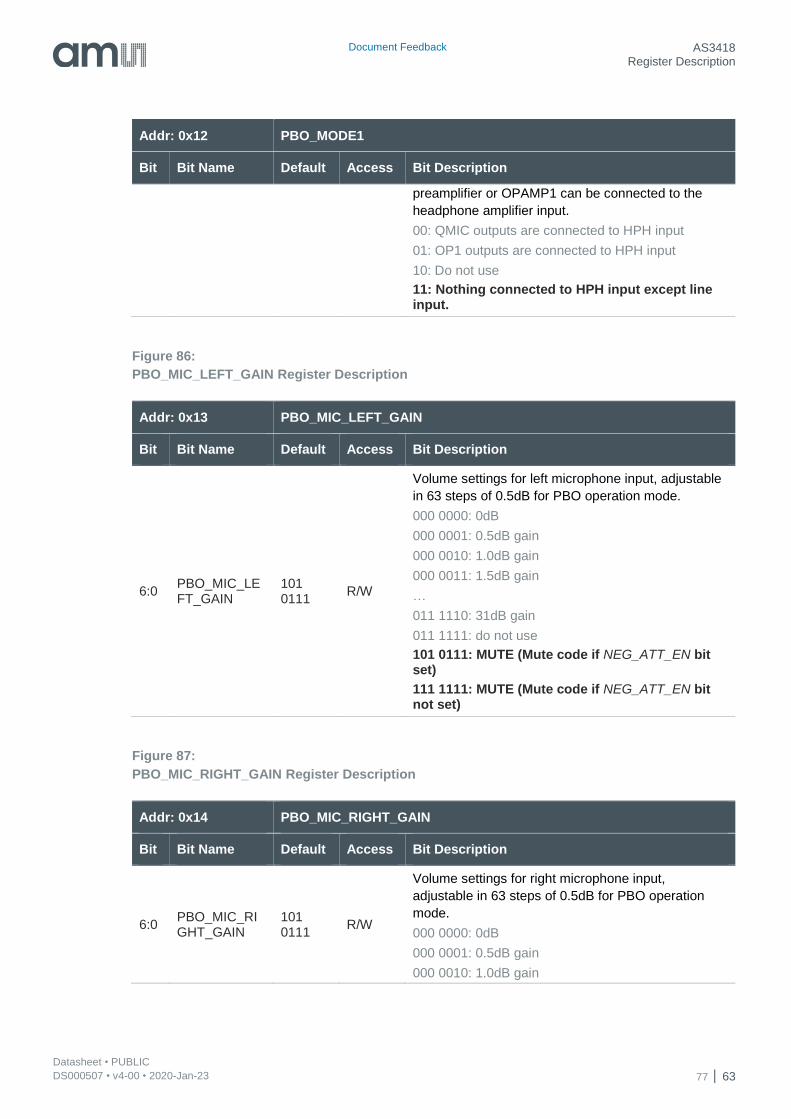
Document Feedback AS3418 Register Description
Datasheet • PUBLIC DS000507 • v4-00 • 2020-Jan-23 77 63
Addr: 0x12 PBO_MODE1
Bit Bit Name Default Access Bit Description
preamplifier or OPAMP1 can be connected to the
headphone amplifier input.
00: QMIC outputs are connected to HPH input
01: OP1 outputs are connected to HPH input
10: Do not use
11: Nothing connected to HPH input except line input.
Figure 86:
PBO_MIC_LEFT_GAIN Register Description
Addr: 0x13 PBO_MIC_LEFT_GAIN
Bit Bit Name Default Access Bit Description
6:0 PBO_MIC_LEFT_GAIN
101 0111
R/W
Volume settings for left microphone input, adjustable
in 63 steps of 0.5dB for PBO operation mode.
000 0000: 0dB
000 0001: 0.5dB gain
000 0010: 1.0dB gain
000 0011: 1.5dB gain
…
011 1110: 31dB gain
011 1111: do not use
101 0111: MUTE (Mute code if NEG_ATT_EN bit set)
111 1111: MUTE (Mute code if NEG_ATT_EN bit not set)
Figure 87:
PBO_MIC_RIGHT_GAIN Register Description
Addr: 0x14 PBO_MIC_RIGHT_GAIN
Bit Bit Name Default Access Bit Description
6:0 PBO_MIC_RIGHT_GAIN
101 0111
R/W
Volume settings for right microphone input,
adjustable in 63 steps of 0.5dB for PBO operation
mode.
000 0000: 0dB
000 0001: 0.5dB gain
000 0010: 1.0dB gain
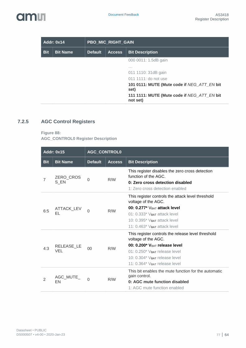
Document Feedback AS3418 Register Description
Datasheet • PUBLIC DS000507 • v4-00 • 2020-Jan-23 77 64
Addr: 0x14 PBO_MIC_RIGHT_GAIN
Bit Bit Name Default Access Bit Description
000 0011: 1.5dB gain
…
011 1110: 31dB gain
011 1111: do not use
101 0111: MUTE (Mute code if NEG_ATT_EN bit set)
111 1111: MUTE (Mute code if NEG_ATT_EN bit not set)
7.2.5 AGC Control Registers
Figure 88:
AGC_CONTROL0 Register Description
Addr: 0x15 AGC_CONTROL0
Bit Bit Name Default Access Bit Description
7 ZERO_CROSS_EN
0 R/W
This register disables the zero cross detection
function of the AGC.
0: Zero cross detection disabled
1: Zero cross detection enabled
6:5 ATTACK_LEVEL
0 R/W
This register controls the attack level threshold
voltage of the AGC.
00: 0.277* VBAT attack level
01: 0.333* VBAT attack level
10: 0.395* VBAT attack level
11: 0.463* VBAT attack level
4:3 RELEASE_LEVEL
00 R/W
This register controls the release level threshold
voltage of the AGC.
00: 0.200* VBAT release level
01: 0.250* VBAT release level
10: 0.304* VBAT release level
11: 0.364* VBAT release level
2 AGC_MUTE_EN
0 R/W
This bit enables the mute function for the automatic gain control.
0: AGC mute function disabled
1: AGC mute function enabled
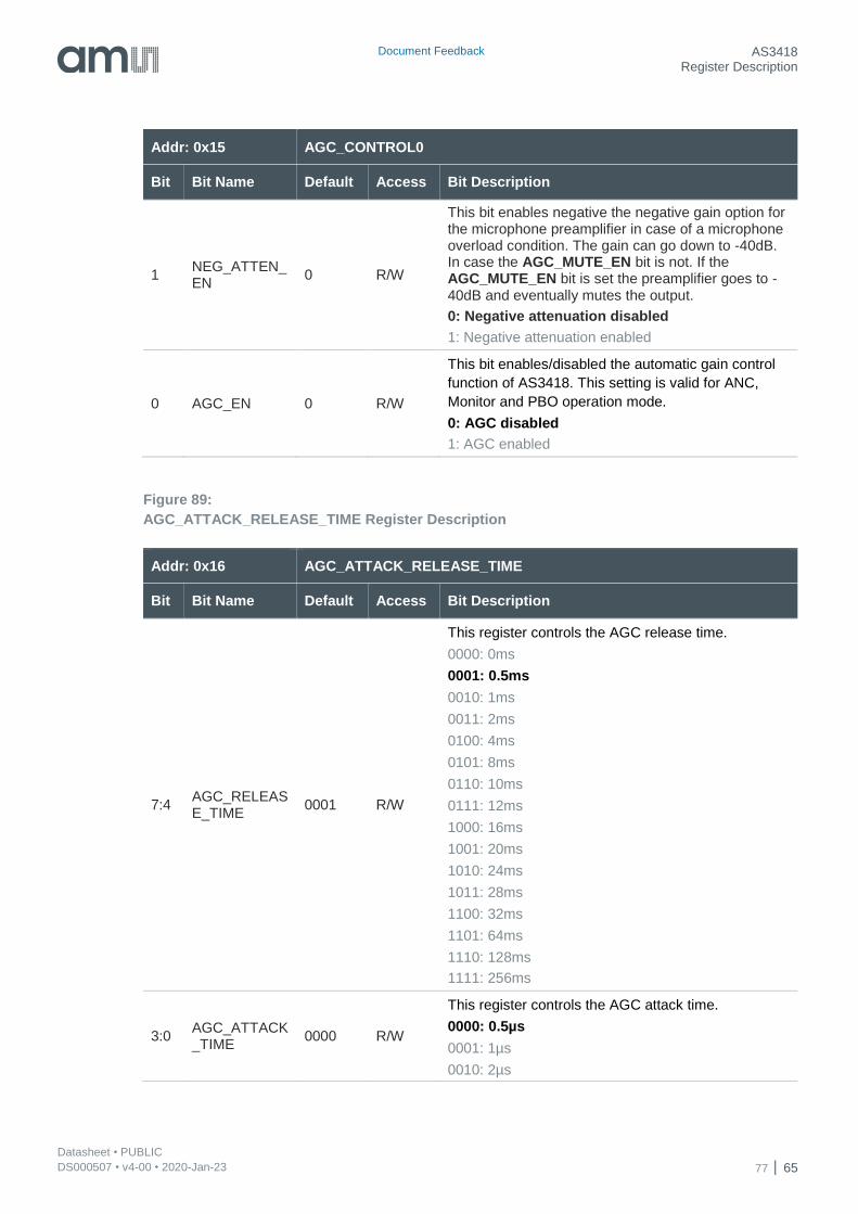
Document Feedback AS3418 Register Description
Datasheet • PUBLIC DS000507 • v4-00 • 2020-Jan-23 77 65
Addr: 0x15 AGC_CONTROL0
Bit Bit Name Default Access Bit Description
1 NEG_ATTEN_EN
0 R/W
This bit enables negative the negative gain option for the microphone preamplifier in case of a microphone overload condition. The gain can go down to -40dB. In case the AGC_MUTE_EN bit is not. If the AGC_MUTE_EN bit is set the preamplifier goes to -40dB and eventually mutes the output.
0: Negative attenuation disabled
1: Negative attenuation enabled
0 AGC_EN 0 R/W
This bit enables/disabled the automatic gain control
function of AS3418. This setting is valid for ANC,
Monitor and PBO operation mode.
0: AGC disabled
1: AGC enabled
Figure 89:
AGC_ATTACK_RELEASE_TIME Register Description
Addr: 0x16 AGC_ATTACK_RELEASE_TIME
Bit Bit Name Default Access Bit Description
7:4 AGC_RELEASE_TIME
0001 R/W
This register controls the AGC release time.
0000: 0ms
0001: 0.5ms
0010: 1ms
0011: 2ms
0100: 4ms
0101: 8ms
0110: 10ms
0111: 12ms
1000: 16ms
1001: 20ms
1010: 24ms
1011: 28ms
1100: 32ms
1101: 64ms
1110: 128ms
1111: 256ms
3:0 AGC_ATTACK_TIME
0000 R/W
This register controls the AGC attack time.
0000: 0.5µs
0001: 1µs
0010: 2µs
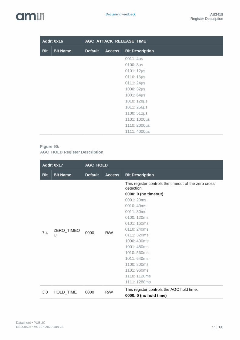
Document Feedback AS3418 Register Description
Datasheet • PUBLIC DS000507 • v4-00 • 2020-Jan-23 77 66
Addr: 0x16 AGC_ATTACK_RELEASE_TIME
Bit Bit Name Default Access Bit Description
0011: 4µs
0100: 8µs
0101: 12µs
0110: 16µs
0111: 24µs
1000: 32µs
1001: 64µs
1010: 128µs
1011: 256µs
1100: 512µs
1101: 1000µs
1110: 2000µs
1111: 4000µs
Figure 90:
AGC_HOLD Register Description
Addr: 0x17 AGC_HOLD
Bit Bit Name Default Access Bit Description
7:4 ZERO_TIMEOUT
0000 R/W
This register controls the timeout of the zero cross detection.
0000: 0 (no timeout)
0001: 20ms
0010: 40ms
0011: 80ms
0100: 120ms
0101: 160ms
0110: 240ms
0111: 320ms
1000: 400ms
1001: 480ms
1010: 560ms
1011: 640ms
1100: 800ms
1101: 960ms
1110: 1120ms
1111: 1280ms
3:0 HOLD_TIME 0000 R/W This register controls the AGC hold time.
0000: 0 (no hold time)
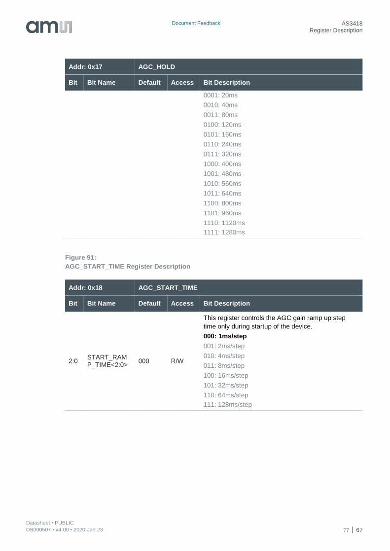
Document Feedback AS3418 Register Description
Datasheet • PUBLIC DS000507 • v4-00 • 2020-Jan-23 77 67
Addr: 0x17 AGC_HOLD
Bit Bit Name Default Access Bit Description
0001: 20ms
0010: 40ms
0011: 80ms
0100: 120ms
0101: 160ms
0110: 240ms
0111: 320ms
1000: 400ms
1001: 480ms
1010: 560ms
1011: 640ms
1100: 800ms
1101: 960ms
1110: 1120ms
1111: 1280ms
Figure 91:
AGC_START_TIME Register Description
Addr: 0x18 AGC_START_TIME
Bit Bit Name Default Access Bit Description
2:0 START_RAMP_TIME<2:0>
000 R/W
This register controls the AGC gain ramp up step
time only during startup of the device.
000: 1ms/step
001: 2ms/step
010: 4ms/step
011: 8ms/step
100: 16ms/step
101: 32ms/step
110: 64ms/step
111: 128ms/step
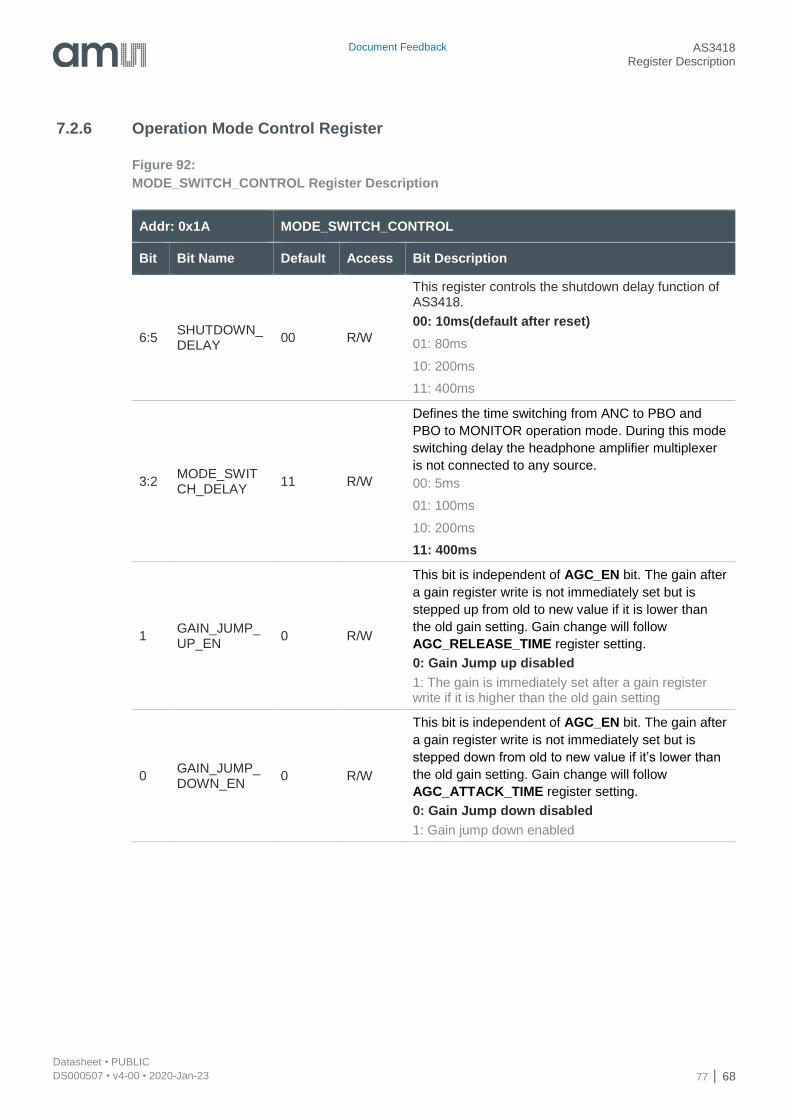
Document Feedback AS3418 Register Description
Datasheet • PUBLIC DS000507 • v4-00 • 2020-Jan-23 77 68
7.2.6 Operation Mode Control Register
Figure 92:
MODE_SWITCH_CONTROL Register Description
Addr: 0x1A MODE_SWITCH_CONTROL
Bit Bit Name Default Access Bit Description
6:5 SHUTDOWN_DELAY
00 R/W
This register controls the shutdown delay function of AS3418.
00: 10ms(default after reset)
01: 80ms
10: 200ms
11: 400ms
3:2 MODE_SWITCH_DELAY
11 R/W
Defines the time switching from ANC to PBO and
PBO to MONITOR operation mode. During this mode
switching delay the headphone amplifier multiplexer
is not connected to any source.
00: 5ms
01: 100ms
10: 200ms
11: 400ms
1 GAIN_JUMP_UP_EN
0 R/W
This bit is independent of AGC_EN bit. The gain after
a gain register write is not immediately set but is
stepped up from old to new value if it is lower than
the old gain setting. Gain change will follow
AGC_RELEASE_TIME register setting.
0: Gain Jump up disabled
1: The gain is immediately set after a gain register write if it is higher than the old gain setting
0 GAIN_JUMP_DOWN_EN
0 R/W
This bit is independent of AGC_EN bit. The gain after
a gain register write is not immediately set but is
stepped down from old to new value if it’s lower than
the old gain setting. Gain change will follow
AGC_ATTACK_TIME register setting.
0: Gain Jump down disabled
1: Gain jump down enabled
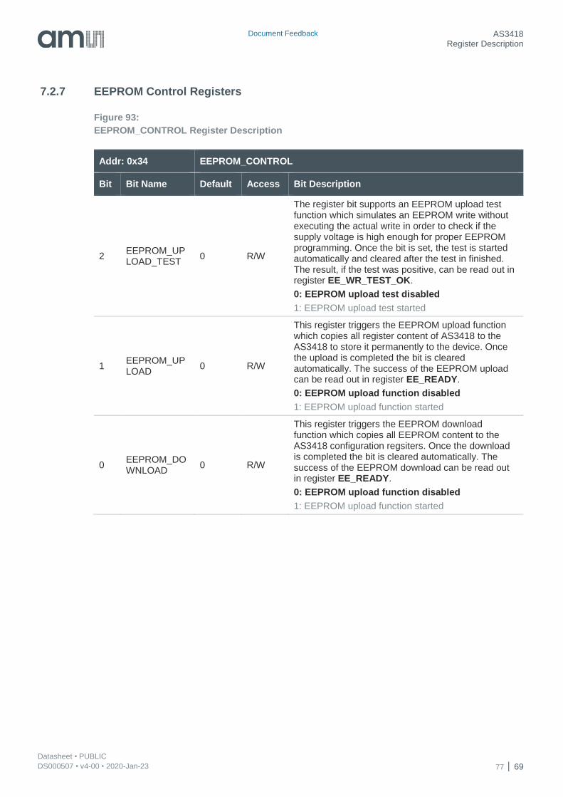
Document Feedback AS3418 Register Description
Datasheet • PUBLIC DS000507 • v4-00 • 2020-Jan-23 77 69
7.2.7 EEPROM Control Registers
Figure 93:
EEPROM_CONTROL Register Description
Addr: 0x34 EEPROM_CONTROL
Bit Bit Name Default Access Bit Description
2 EEPROM_UPLOAD_TEST
0 R/W
The register bit supports an EEPROM upload test function which simulates an EEPROM write without executing the actual write in order to check if the supply voltage is high enough for proper EEPROM programming. Once the bit is set, the test is started automatically and cleared after the test in finished. The result, if the test was positive, can be read out in register EE_WR_TEST_OK.
0: EEPROM upload test disabled
1: EEPROM upload test started
1 EEPROM_UPLOAD
0 R/W
This register triggers the EEPROM upload function which copies all register content of AS3418 to the AS3418 to store it permanently to the device. Once the upload is completed the bit is cleared automatically. The success of the EEPROM upload can be read out in register EE_READY.
0: EEPROM upload function disabled
1: EEPROM upload function started
0 EEPROM_DOWNLOAD
0 R/W
This register triggers the EEPROM download function which copies all EEPROM content to the AS3418 configuration regsiters. Once the download is completed the bit is cleared automatically. The success of the EEPROM download can be read out in register EE_READY.
0: EEPROM upload function disabled
1: EEPROM upload function started
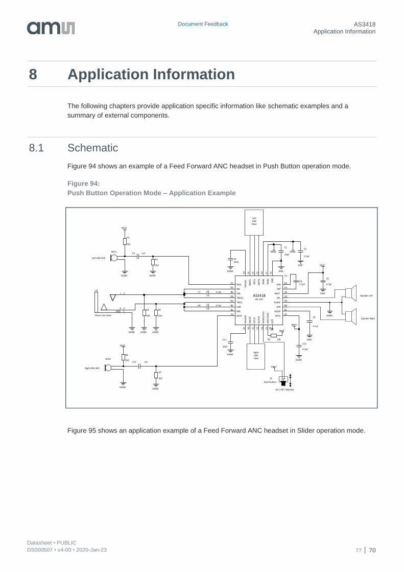
Document Feedback AS3418 Application Information
Datasheet • PUBLIC DS000507 • v4-00 • 2020-Jan-23 77 70
8 Application Information
The following chapters provide application specific information like schematic examples and a
summary of external components.
8.1 Schematic
Figure 94 shows an example of a Feed Forward ANC headset in Push Button operation mode.
Figure 94:
Push Button Operation Mode – Application Example
Figure 95 shows an application example of a Feed Forward ANC headset in Slider operation mode.
4.7µF
C5
2.2µFC6
GND
VBAT
3
12
L
RGND
U2
Music Line Input
AGND
MIC1
Left ANC MIC
2k2
R1
4.7µF
C9
4.7µF
C12
GND
MICS
AGND
1uFC3
10uFC4
AGND
MIC2
Right ANC MIC
2k2
R6
MICS
1uFC13
AGND
10uF
C11
AGND
2k2
R7
AGND
2k2
R2
AGND
150
R3
150
R4
AGND AGND
4.7µFC7
4.7µFC8
IOP
1RA
1
QO
P1R
C2
VBATA6
VNEG
A4
GN
DA
5
CPPC4
BPRB1
HPRB2
QM
ICR
A2
CPNB4
LINRB5
LINLB6
VNEG
C1
HPLD2
QM
ICL
E2
MICSE4
AN
C/CS
DA
C6
MO
DE/
CS
CL
C5
BPLD1
QO
P1L
C3
MSUPE5
MIC
ACL
D3
TRSDAD4
TRSCLD6
IOP
1LE1
AGNDD5
ILED
E6
MICLE3
MICRA3
MIC
ACR
B3
AS3418WL-CSP
U1
VNEG10µF
C1
GND
2.2µF
C2
GND
VNEG
MICS
AGND
AGND
Speaker Left
Speaker Right
LeftANCFilter
RightANCFilter
On / Off / Monitor
VBAT
Push Button
S1
VBAT
R5 10k
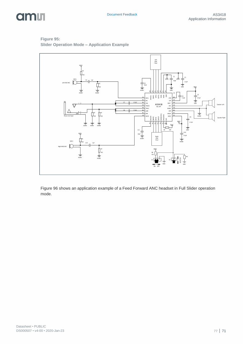
Document Feedback AS3418 Application Information
Datasheet • PUBLIC DS000507 • v4-00 • 2020-Jan-23 77 71
Figure 95:
Slider Operation Mode – Application Example
Figure 96 shows an application example of a Feed Forward ANC headset in Full Slider operation
mode.
S2
VBAT
GND
MO
NIT
OR
S3
GND
ON OFF
R8
22k
R9
4.7µF
C5
2.2µFC6
GND
VBAT
3
12
L
RGND
U2
Music Line Input
AGND
MIC1
Left ANC MIC
2k2
R1
4.7µF
C9
4.7µF
C12
GND
MICS
AGND
1uFC3
10uFC4
AGND
MIC2
Right ANC MIC
2k2
R6
MICS
1uFC13
AGND
10uF
C11
AGND
2k2
R7
AGND
2k2
R2
AGND
150
R3
150
R4
AGND AGND
4.7µFC7
4.7µFC8
IOP
1RA
1
QO
P1R
C2
VBATA6
VNEG
A4
GN
DA
5
CPPC4
BPRB1
HPRB2
QM
ICR
A2
CPNB4
LINRB5
LINLB6
VNEG
C1
HPLD2
QM
ICL
E2
MICSE4
AN
C/CS
DA
C6
MO
DE/
CS
CL
C5
BPLD1
QO
P1L
C3
MSUPE5
MIC
AC
LD
3
TRSDAD4
TRSCLD6
IOP
1LE1
AGNDD5
ILED
E6
MICLE3
MICRA3
MIC
ACR
B3
AS3418WL-CSP
U1
VNEG10µF
C1
GND
2.2µF
C2
GND
VNEG
MICS
AGND
AGND
Speaker Left
Speaker Right
LeftANCFilter
RightANCFilter
VBAT
R5 10k
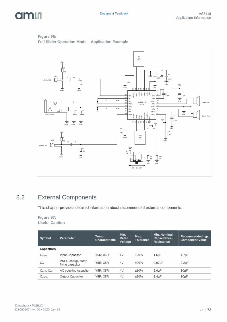
Document Feedback AS3418 Application Information
Datasheet • PUBLIC DS000507 • v4-00 • 2020-Jan-23 77 72
Figure 96:
Full Slider Operation Mode – Application Example
8.2 External Components
This chapter provides detailed information about recommended external components.
Figure 97:
Useful Caption
Symbol Parameter Temp. Characteristic
Min. Rated Voltage
Max. Tolerance
Min. Nominal Capacitance / Resistance
Recommended typ. Component Value
Capacitors
CVBAT Input Capacitor Y5R; X5R 4V ±20% 1.6µF 4.7µF
CFLY VNEG charge pump flying capacitor
Y5R; X5R 4V ±20% 0.97µF 2.2µF
CACR, CACL AC coupling capacitor Y5R; X5R 4V ±10% 5.6µF 10µF
CVNEG Output Capacitor Y5R; X5R 4V ±20% 3.4µF 10µF
VBAT
GND GND
R9
22k
R10
1M
OFF ON MON
R8
22k
4.7µF
C5
2.2µFC6
GND
VBAT
3
12
L
RGND
U2
Music Line Input
AGND
MIC1
Left ANC MIC
2k2
R1
4.7µF
C9
4.7µF
C12
GND
MICS
AGND
1uFC3
10uFC4
AGND
MIC2
Right ANC MIC
2k2
R6
MICS
1uFC13
AGND
10uF
C11
AGND
2k2
R7
AGND
2k2
R2
AGND
150
R3
150
R4
AGND AGND
4.7µFC7
4.7µFC8
IOP
1RA
1
QO
P1R
C2
VBATA6
VNEG
A4
GN
DA
5
CPPC4
BPRB1
HPRB2
QM
ICR
A2
CPNB4
LINRB5
LINLB6
VNEG
C1
HPLD2
QM
ICL
E2
MICSE4
AN
C/C
SD
A
C6
MO
DE/
CSCL
C5
BPLD1
QO
P1L
C3
MSUPE5
MIC
ACL
D3
TRSDAD4
TRSCLD6
IOP
1LE1
AGNDD5
ILED
E6
MICLE3
MICRA3
MIC
ACR
B3
AS3418WL-CSP
U1
VNEG10µF
C1
GND
2.2µF
C2
GND
VNEG
MICS
AGND
AGND
Speaker Left
Speaker Right
LeftANCFilter
RightANCFilter
VBAT
R5 10k
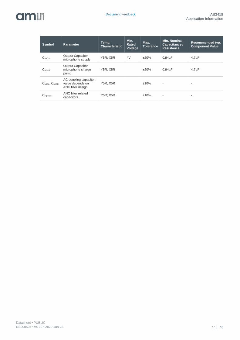
Document Feedback AS3418 Application Information
Datasheet • PUBLIC DS000507 • v4-00 • 2020-Jan-23 77 73
Symbol Parameter Temp. Characteristic
Min. Rated Voltage
Max. Tolerance
Min. Nominal Capacitance / Resistance
Recommended typ. Component Value
CMICS Output Capacitor microphone supply
Y5R; X5R 4V ±20% 0.94µF 4.7µF
CMSUP Output Capacitor microphone charge pump
Y5R; X5R ±20% 0.94µF 4.7µF
CMICL, CMICR AC coupling capacitor; value depends on ANC filter design
Y5R; X5R ±10% - -
CFILTER ANC filter related capacitors
Y5R; X5R ±10% - -
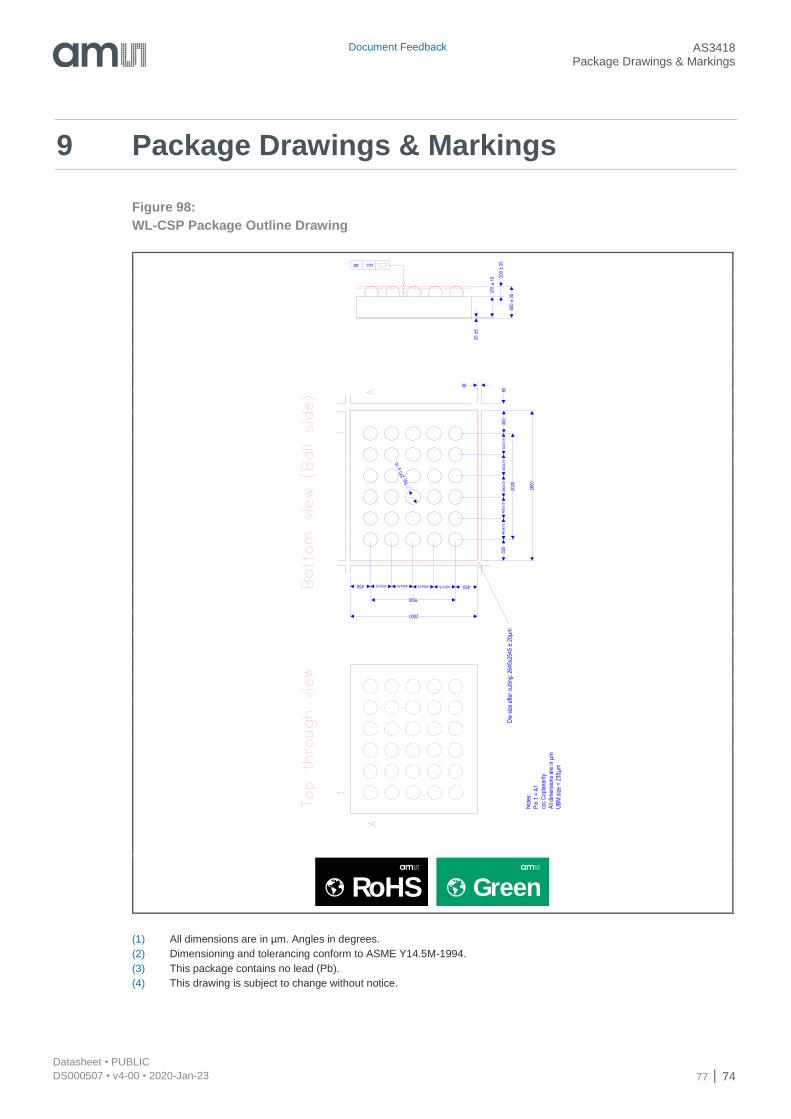
Document Feedback AS3418 Package Drawings & Markings
Datasheet • PUBLIC DS000507 • v4-00 • 2020-Jan-23 77 74
9 Package Drawings & Markings
Figure 98:
WL-CSP Package Outline Drawing
(1) All dimensions are in µm. Angles in degrees.
(2) Dimensioning and tolerancing conform to ASME Y14.5M-1994.
(3) This package contains no lead (Pb).
(4) This drawing is subject to change without notice.
400±
1530
080
80
ccc40
25 ±
5
375
± 1
5 200
± 2
0
600
± 3
0D
ie s
ize
afte
r cu
tting
: 264
5x25
45 ±
20µ
m
Not
es:
Pin
1 =
A1
ccc
Cop
lana
rity
All
dim
ensi
ons
are
in µ
m
UB
M s
ize
= 2
35µ
m
400±
1540
0±15
400±
1540
0±15
300
2600
450400±15400±15450
2500
typ.
270
± 1
0
2000
1600
400±15 400±15
RoHS Green
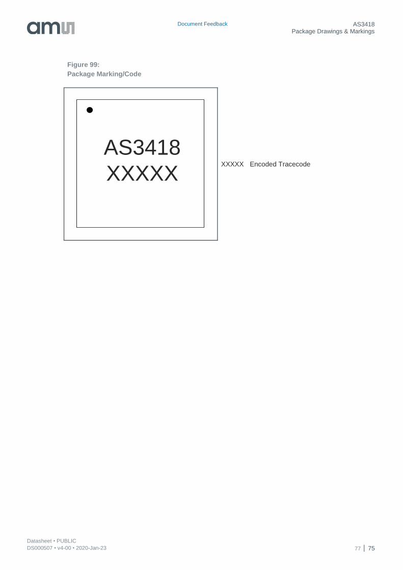
Document Feedback AS3418 Package Drawings & Markings
Datasheet • PUBLIC DS000507 • v4-00 • 2020-Jan-23 77 75
Figure 99:
Package Marking/Code
XXXXX Encoded Tracecode
AS3418
XXXXX
Document Feedback AS3418 Revision Information
Datasheet • PUBLIC DS000507 • v4-00 • 2020-Jan-23 77 76
10 Revision Information
Document Status Product Status Definition
Product Preview Pre-Development Information in this datasheet is based on product ideas in the planning phase of development. All specifications are design goals without any warranty and are subject to change without notice
Preliminary Datasheet Pre-Production Information in this datasheet is based on products in the design, validation or qualification phase of development. The performance and parameters shown in this document are preliminary without any warranty and are subject to change without notice
Datasheet Production Information in this datasheet is based on products in ramp-up to full production or full production which conform to specifications in accordance with the terms of ams AG standard warranty as given in the General Terms of Trade
Datasheet (discontinued)
Discontinued Information in this datasheet is based on products which conform to specifications in accordance with the terms of ams AG standard warranty as given in the General Terms of Trade, but these products have been superseded and should not be used for new designs
Changes from previous version to current revision v4-00 Page
Figure 94 update of ball number of pin QOP1L 70
Figure 95 update of ball number of pin QOP1L 71
Figure 96 update of ball number of pin QOP1L 72
Page and figure numbers for the previous version may differ from page and figure numbers in the current revision.
Correction of typographical errors is not explicitly mentioned.
Document Feedback AS3418 Legal Information
Datasheet • PUBLIC DS000507 • v4-00 • 2020-Jan-23 77 77
11 Legal Information
Copyrights & Disclaimer
Copyright ams AG, Tobelbader Strasse 30, 8141 Premstaetten, Austria-Europe. Trademarks Registered. All rights reserved. The material herein may not be reproduced, adapted, merged, translated, stored, or used without the prior written consent of the copyright owner.
Devices sold by ams AG are covered by the warranty and patent indemnification provisions appearing in its General Terms of Trade. ams AG makes no warranty, express, statutory, implied, or by description regarding the information set forth herein. ams AG reserves the right to change specifications and prices at any time and without notice. Therefore, prior to designing this product into a system, it is necessary to check with ams AG for current information. This product is intended for use in commercial applications. Applications requiring extended temperature range, unusual environmental requirements, or high reliability applications, such as military, medical life-support or life-sustaining equipment are specifically not recommended without additional processing by ams AG for each application. This product is provided by ams AG “AS IS” and any express or implied warranties, including, but not limited to the implied warranties of merchantability and fitness for a particular purpose are disclaimed.
ams AG shall not be liable to recipient or any third party for any damages, including but not limited to personal injury, property damage, loss of profits, loss of use, interruption of business or indirect, special, incidental or consequential damages, of any kind, in connection with or arising out of the furnishing, performance or use of the technical data herein. No obligation or liability to recipient or any third party shall arise or flow out of ams AG rendering of technical or other services.
RoHS Compliant & ams Green Statement
RoHS Compliant: The term RoHS compliant means that ams AG products fully comply with current RoHS directives. Our semiconductor products do not contain any chemicals for all 6 substance categories plus additional 4 substance categories (per amendment EU 2015/863), including the requirement that lead not exceed 0.1% by weight in homogeneous materials. Where designed to be soldered at high temperatures, RoHS compliant products are suitable for use in specified lead-free processes.
ams Green (RoHS compliant and no Sb/Br/Cl): ams Green defines that in addition to RoHS compliance, our products are free of Bromine (Br) and Antimony (Sb) based flame retardants (Br or Sb do not exceed 0.1% by weight in homogeneous material) and do not contain Chlorine (Cl not exceed 0.1% by weight in homogeneous material).
Important Information: The information provided in this statement represents ams AG knowledge and belief as of the date that it is provided. ams AG bases its knowledge and belief on information provided by third parties, and makes no representation or warranty as to the accuracy of such information. Efforts are underway to better integrate information from third parties. ams AG has taken and continues to take reasonable steps to provide representative and accurate information but may not have conducted destructive testing or chemical analysis on incoming materials and chemicals. ams AG and ams AG suppliers consider certain information to be proprietary, and thus CAS numbers and other limited information may not be available for release.
Headquarters
ams AG
Tobelbader Strasse 30
8141 Premstaetten
Austria, Europe
Tel: +43 (0) 3136 500 0
Please visit our website at www.ams.com
Buy our products or get free samples online at www.ams.com/Products
Technical Support is available at www.ams.com/Technical-Support
Provide feedback about this document at www.ams.com/Document-Feedback
For sales offices, distributors and representatives go to www.ams.com/Contact
For further information and requests, e-mail us at [email protected]


![How to read a datasheet - english version[1]](https://img.pdfslide.net/doc/110x75/577d2da91a28ab4e1eae0a71/how-to-read-a-datasheet-english-version1.jpg)