Embed Size (px)
Citation preview

© OCR 2008 QAN (500/2581/8) QAN (500/2583/1)
AS/A Level GCE
GCE Electronics OCR Advanced Subsidiary GCE in Electronics H065
OCR Advanced GCE in Electronics H465
vers
ion
2 –
Febr
uary
200
8

Contents
2 © OCR 2008 GCE Electronics – version 2
1 About these Qualifications 4
1.1 The Three-Unit AS 4 1.2 The Six-Unit Advanced GCE 4 1.3 Qualification Titles and Levels 4 1.4 Aims 5 1.5 Prior Learning/Attainment 5
2 Summary of Content 6
2.1 AS Units 6 2.2 A2 Units 6
3 Unit Content 8
3.1 AS Unit F611: Simple Systems 8 3.2 AS Unit F612: Signal Processors 14 3.3 AS Unit F613: Build and Investigate Electronic Circuits 18 3.4 A2 Unit F614: Electronic Control Systems 20 3.5 A2 Unit F615: Communication Systems 25 3.6 A2 Unit F616: Design, Build and Investigate Electronic Circuits 32
4 Schemes of Assessment 34
4.1 AS GCE Scheme of Assessment 34 4.2 Advanced GCE Scheme of Assessment 35 4.3 Unit Order 36 4.4 Unit Options (at AS/A2) 36 4.5 Synoptic Assessment (A Level GCE) 36 4.6 Assessment Availability 36 4.7 Assessment Objectives 37 4.8 Quality of Written Communication 38
5 Technical Information 39
5.1 Making Unit Entries 39 5.2 Making Qualification Entries 39 5.3 Grading 39 5.4 Result Enquiries and Appeals 40 5.5 Shelf-Life of Units 40 5.6 Unit and Qualification Re-sits 40 5.7 Guided Learning Hours 41 5.8 Code of Practice/Subject Criteria/Common Criteria Requirements 41 5.9 Arrangements for Candidates with Particular Requirements 41 5.10 Prohibited Qualifications and Classification Code 41 5.11 Coursework Administration/Regulations 41

© OCR 2008 GCE Electronics – version 2 3
6 Other Specification Issues 43
6.1 Overlap with other Qualifications 43 6.2 Progression from these Qualifications 43 6.3 Key Skills Mapping 43 6.4 Spiritual, Moral, Ethical, Social, Legislative, Economic and Cultural Issues 44 6.5 Sustainable Development, Health and Safety Considerations and European Developments 44 6.6 Avoidance of Bias 44 6.7 Language 44 6.8 Disability Discrimination Act Information Relating to these Specifications 45
Appendix A: Performance Descriptions 46
Appendix B: Coursework Assessment Criteria for AS Unit F613: Build and Investigate Electronic Circuits 49
Appendix C: Suggested Investigations for AS Unit F613: Build and Investigate Electronic Circuits 53
Appendix D: Investigation Assessment Criteria for A2 Unit F616: Design, Build and Investigate Electronic Circuits 54
Appendix E: Suggested Investigations for A2 Unit F616: Design, Build and Investigate Electronic Circuits 57
Appendix F: Formulae Relationships and Boolean Algebra 59
Appendix G: Microcontroller flowchart symbols 61
Appendix H: Assembler Codes 63
Appendix I: Standard Circuit Symbols 64
Vertical black lines indicate a significant change to the previous printed version. Changes can be found on pages 26, 63, 64 and 65.

4 © OCR 2008 GCE Electronics – version 2
1 About these Qualifications This booklet contains OCR’s Advanced Subsidiary (AS) GCE and Advanced GCE specifications in electronics for teaching from September 2008.
These AS GCE and Advanced GCE specifications aim to provide an introduction to and thorough grounding in electronics. They are designed around a systems approach to electronics that introduces a wide range of transducers and input, output and processing systems and encourages a practical, problem-solving approach. Project work allows the development of skills and the application of knowledge in the solution of a practical problem. The specifications aim to give an introduction to the electronics involved in modern communication and control systems.
1.1 The Three-Unit AS
The Advanced Subsidiary GCE is both a ‘stand-alone’ qualification and also the first half of the corresponding Advanced GCE. The AS GCE is assessed at a standard appropriate for candidates who have completed the first year of study (both in terms of teaching time and content) of the corresponding two-year Advanced GCE course, ie between GCSE and Advanced GCE.
From September 2008 The AS GCE is made up of three mandatory units, of which two are externally assessed and one is internally assessed. These units form 50% of the corresponding six-unit Advanced GCE.
1.2 The Six-Unit Advanced GCE
From September 2008 The Advanced GCE is made up of three mandatory units at AS and three further units at A2. Two A2 units are externally assessed and one A2 unit is internally assessed.
1.3 Qualification Titles and Levels
These qualifications are shown on a certificate as:
• OCR Advanced Subsidiary GCE in Electronics.
• OCR Advanced GCE in Electronics.
Both qualifications are Level 3 in the National Qualification Framework (NQF).

© OCR 2008 GCE Electronics – version 2 5
1.4 Aims
The aims of these specifications are to:
• develop and sustain an interest in and an enjoyment of electronics and its applications;
• develop an awareness and an understanding of the social and economic implications of electronics;
• develop knowledge and understanding of the principles of electronics that are desirable in a technologically-based society;
• develop an appropriate body of knowledge for those not studying the subject beyond this stage, which will also serve as a foundation for more advanced studies in electronics;
• develop the skills of observation, experimentation and the processing and interpretation of data;
• apply qualitatively and quantitatively their knowledge and understanding of electronic principles;
• apply a logical approach to the analysis and synthesis of complex systems;
• develop the practical skills associated with the design, construction and testing of electronic systems;
• foster relevant communication skills.
1.5 Prior Learning/Attainment
No prior knowledge of the subject is required. The specifications build on, but do not depend on, the knowledge, understanding and skills specified for GCSE Electronics. It is recommended that candidates have attained communication and literacy skills at a level equivalent to GCSE Grade C in English.
The specifications have been written without assuming that candidates will be taking A Level Mathematics or Physics in conjunction with the course. However, prior acquaintance with relevant parts of GCSE Mathematics and Science specifications would be an advantage. It is assumed that any tuition needed to cope with the mathematics implied by the specifications would be provided to supplement the basic teaching of the specifications.

6 © OCR 2008 GCE Electronics – version 2
2 Summary of Content
2.1 AS Units
Unit F611: Simple Systems
• Simple Digital Systems
• Digital from Analogue
• Pulses
• Logic Systems
Unit F612: Signal Processors
• Storing signals
• Negative feedback
• Counting pulses
• Amplifying audio
• Microcontrollers
Unit F613: Build and Investigate Electronic Circuits
Three short tasks:
• a digital circuit;
• an analogue circuit that uses an op-amp;
• a microcontroller circuit in which the microcontroller has been programmed using a flowchart technique.
2.2 A2 Units
Unit F614: Electronic Control Systems
• MOSFET Circuits
• Digital Processing
• Servo Control
• Microcontroller Systems

© OCR 2008 GCE Electronics – version 2 7
Unit F615: Communication Systems
• Video Displays
• Modulating Carriers
• Frequency Division Multiplexing
• Time Division Multiplexing
Unit F616: Design, Build and Investigate Electronic Circuits
• A single project in which candidates design, build, test and analyse a circuit that serves a useful purpose

8 © OCR 2008 GCE Electronics – version 2
3 Unit Content
3.1 AS Unit F611: Simple Systems
This unit introduces candidates to the fundamentals of modern electronics.
This includes the use of:
• basic equations to calculate quantities;
• standard prefixes and units to state values of quantities;
• standard circuit symbols in circuit diagrams;
• measuring instruments;
• models for voltage, current and power in circuits;
• block diagrams to analyse circuits;
• passive and active components to generate, process and display signals;
• truth tables, Boolean algebra and graphs to represent the transfer characteristics of components and systems.
It is recommended that candidates are familiar with the following areas.
Candidates should know and understand:
• the concepts of conductors and insulators in terms of the mobility of charge;
• voltage as a measure of the energy per charge at a point in a circuit;
• current as the rate of transfer of charge past a point in a circuit;
• need for a power supply to maintain a current in a circuit;
• the conversion of energy from electrical to other forms as charge moves round a circuit;
• the behaviour of currents at a junction;
• the voltage across a series circuit is the sum of the voltage across the components;
• the current in a series circuit is the same in all the components.

© OCR 2008 GCE Electronics – version 2 9
1.1 Simple Digital Systems
Switches in series with resistors can be used to convert information into digital signals.
Candidates should be able to: (a) recall how to use switches and pull-up or pull-
down resistors in series with a power supply to generate digital signals;
(b) recall that, unless otherwise stated, logic 1 (high) is a signal at +5 V and logic 0 (low) is a signal at 0 V;
(c) recall and use the defining equation for
resistance (IVR = );
(d) recall and use the equation for power ( VIP = ) to calculate the rate of heating, or output power, of a component;
(e) recall that components have maximum ratings for current, voltage or power;
(f) recall how to use multimeters as voltmeters, ammeters and ohmmeters to measure voltage, current and resistance in a circuit;
(g) understand the use of the prefixes G, M, k, m, μ, n and p when calculating values of quantities.
Digital signals can be processed by logic gates. Candidates should be able to: (h) recall the transfer characteristic of a NOT
gate (an input above +3 V gives 0 V at the output, an input below +2 V gives +5 V at the output), and represent it as an input–output graph;
(i) recall the truth tables of the following two-input logic gates: AND, EOR, NAND, NOR, OR;
(j) understand the use of an LED to indicate the state of a logic gate's output (including the need for a series resistor);
(k) recall the transfer characteristic of an LED and represent it as a current–voltage graph (no current in reverse bias; current rises rapidly in forward bias when voltage reaches 2 V).

10 © OCR 2008 GCE Electronics – version 2
A logic gate’s output signal can be used to switch a variety of devices on and off via a driver.
Candidates should be able to: (a) recall that logic gates can only source or sink
currents of a few milliamps, so cannot supply much power to output devices;
(b) understand that a MOSFET is a voltage-controlled resistor (the voltage at the gate determines the resistance between the drain and the source);
(c) recall the transfer characteristic of a MOSFET (drain-source resistance is infinite until gate-source voltage reaches a threshold value, then drops to a constant low value for higher gate-source voltages) and represent it as a resistance-voltage graph.
(d) recall that MOSFETS with appropriate threshold voltages can act as drivers, sinking current from motors, heaters, buzzers and lamps.
Standard symbols are used to draw circuit diagrams. The flow of information through a system can be shown with block diagrams.
Candidates should be able to: (e) recall and use standard circuit symbols to
draw circuit diagrams; (f) understand that circuit diagrams omit power
supply connections for integrated circuits; (g) represent a simple digital system as a block
diagram, showing input, processing and output stages;
(h) understand that a block diagram shows the flow of information through a system;
(i) understand that block diagrams make it easier to analyse the operation of a system;
(j) analyse and synthesise circuit and block diagrams for digital systems with only one logic gate.

© OCR 2008 GCE Electronics – version 2 11
1.2 Digital from Analogue
The resistance of some components depends on their environment. They can be used as sensors.
Candidates should be able to: (a) recall the transfer characteristic of an LDR
(resistance falls as light intensity increases) and represent this as a resistance–intensity graph;
(b) recall the transfer characteristic of a thermistor (resistance falls as temperature increases) and represent this as a resistance–temperature graph;
(c) recall and use the equation for the resistance of resistors in series (R = R1 + R2) and parallel;
(d) calculate the output voltage of an unloaded voltage divider made from a pair of resistors in series with a power supply;
(e) understand the use of a potentiometer to generate a signal of variable voltage;
(f) understand the difference between analogue and digital signals (analogue have any value, digital have just two).
Op-amps can convert the analogue signal from a sensor into a digital signal for a logic system.
Candidates should be able to: (g) recall the transfer characteristic of an open-
loop op-amp operating from supply rails at +15 V and –15 V (output saturates at +13 V if non-inverting input higher than inverting input, otherwise output saturates at –13 V);
(h) understand that an ideal op-amp can be modelled as having no current at its inputs, but able to source or sink currents of up to 10 mA;
(i) understand the use of a diode in series with resistors to convert the output of an op-amp into high and low signals for a logic system;
(j) recall the transfer characteristic for a diode and represent it as a current–voltage graph (no current in reverse bias; current rises rapidly in forward bias when voltage reaches 0.7 V);
(k) understand the use of a zener diode in series with a resistor to generate a fixed voltage at one of the inputs of an op-amp;
(l) recall the transfer characteristic for a zener diode and represent it as a current-voltage graph (no current in reverse bias until the breakdown voltage; current rises rapidly in forward bias when voltage reaches 0.7 V);
(m) analyse and synthesise sensor systems with digital outputs for position, light intensity and temperature.

12 © OCR 2008 GCE Electronics – version 2
Capacitors can delay the change of a signal. Candidates should be able to: (n) recall the exponential change in voltage
across a capacitor as it is charged or discharged from a constant voltage through a resistor, and represent it as a voltage–time graph;
(o) recall and use the equation for time constant ( RC=τ );
(p) recall and use the idea that the voltage across the resistor of an RC series circuit is halved in a time of 0.7τ;
(q) understand the use of a capacitor to delay the change of signal caused by the closing or opening of a switch in series with a resistor.
1.3 Pulses
A monostable uses an RC network to generate a single pulse.
Candidates should be able to: (a) understand the use of an RC network to
generate spikes from rising or falling edges, representing them as voltage–time graphs at input and output (exponential drop lasts about two time constants);
(b) understand the use of diodes as clamps to suppress spikes from RC networks;
(c) understand the use of a pair of NAND gates and an RC network to make a monostable the output of which goes low for 0.7RC s when triggered by a falling edge;
(d) recall that inputs to logic gates draw no current and have clamping diodes to the supply rails;
(e) sketch voltage–time graphs at inputs and outputs of the logic gates in a monostable.
© OCR 2008 GCE Electronics – version 2 13
A relaxation oscillator uses a Schmitt trigger NOT gate to produce a continuous train of pulses.
Candidates should be able to: (f) recall the transfer characteristic of a Schmitt
trigger NOT gate and represent it as an input–output graph (no recall of trip point values required);
(g) understand the use of an RC network and Schmitt trigger NOT gate to make an oscillator and sketch voltage–time graphs at input and output (period T = 0.5RC);
(h) understand how to use an oscilloscope to observe voltages that vary with time (including use of timebase and vertical amplifier settings to measure amplitude and period);
(i) recall and use the equation for frequency
(T
f 1= );
(j) understand the use of a driver to provide the interface between an oscillator and a loudspeaker.
1.4 Logic Systems
Combinations of logic gates can process signals in many different ways.
Candidates should be able to: (a) understand the use of truth tables to analyse
the behaviour of logic systems with up to three inputs;
(b) recall and use Boolean algebra to represent the output of logic gates;
(c) recall and use Boolean algebra to represent the output columns of a truth table;
(d) understand the construction of a truth table from a Boolean algebra expression;
(e) understand the use of Boolean algebra to represent the behaviour of a logic system (including the use of the rules given in Appendix B to simplify expressions);
(f) synthesise AND, OR and NOT gates from NAND gates;
(g) understand the use of NAND gates to synthesise logic systems with up to four inputs;
(h) understand the advantages of only using NAND gates (more economic use of integrated circuits, economies of scale);
(i) analyse the behaviour of logic systems with up to four inputs and four outputs.

14 © OCR 2008 GCE Electronics – version 2
3.2 AS Unit F612: Signal Processors
This module introduces candidates to systems that process signals through a series of subsystems. This includes the use of:
• bistables, latches and flip-flops to store digital information;
• op-amps as voltage, power and summing amplifiers to process audio frequency signals;
• counters to record pulses and generate sequences of digital signals;
• microcontrollers as programmable devices.
Recommended Prior Knowledge
Candidates should have studied Unit F611 (Simple Systems).
2.1 Storing Signals
Arrays of logic gates can be used to store information.
Candidates should be able to: (a) recall the behaviour of a bistable (separate
inputs to set and reset a single output) and represent its behaviour with timing diagrams;
(b) understand the use of NOR gates to make a bistable with active high inputs;
(c) understand the use of NAND gates to make a bistable with active–low inputs;
(d) recall the behaviour of a latch (data and enable inputs to set and reset a single output) and represent its behaviour with timing diagrams;
(e) analyse the operation of a latch made from logic gates and a bistable;
(f) recall the behaviour of a rising-edge triggered D flip-flop (data, clock, set and reset inputs, complementary outputs) and represent its behaviour with timing diagrams;
(g) analyse the operation of a D flip-flop made from a master–slave pair of latches;
(h) understand the use of an array of D flip-flops to store a binary word.
© OCR 2008 GCE Electronics – version 2 15
2.2 Negative Feedback
Negative feedback allows op-amps to process audio signals.
Candidates should be able to: (a) recall the use of an electret microphone to
transfer sounds into electrical signals, to include the use of a pull-up resistor and a coupling capacitor;
(b) understand that an ideal amplifier increases the amplitude of an ac signal without altering its frequency or shape;
(c) recall and use the equation for voltage gain
(in
outVV
G = );
(d) recall that an op-amp is a differential amplifier (Vout = A(V+ – V-)) with a very large open-loop gain A;
(e) understand the use of negative feedback to make an op-amp into a voltage follower, including the need for a pull-down resistor at the non-inverting input;
(f) understand that a voltage follower has a voltage gain of one but can provide power gain.
Resistors can be used to make op-amps into non-inverting, inverting and summing amplifiers.
Candidates should be able to: (g) understand the use of feedback and pull-
down resistors to make an op-amp into an non-inverting amplifier with a known voltage
gain (d
fRR
G += 1 );
(h) understand the use of feedback and input resistors to make an op-amp into an inverting amplifier with a known voltage gain
(in
fRR
G −= ), to include the concept of virtual
earth for the inverting input; (i) recall the transfer characteristics of inverting
and non-inverting amplifiers based on op-amps, and represent them as input–output graphs, including saturation;
(j) understand the use of feedback and input resistors to allow an op-amp to combine two or more different ac signals
( ...2
2
1
1RV
RV
RV
f
out +=− );
(k) recall that resistors in op-amp amplifiers need to be in the range 1 kΩ to 10 MΩ.

16 © OCR 2008 GCE Electronics – version 2
2.3 Counting Pulses
Arrays of D flip-flops can count pulses. Candidates should be able to: (a) understand the connection of D to Q to make
a D flip-flop into a one-bit counter; (b) understand the use of D flip-flops and a NOT
gate to make a binary ripple up-counter; (c) understand the use of logic gates to make
binary counters that reset to m after n counts, where m and n are integers.
(d) recall and use timing diagrams to represent the transfer characteristics of a binary counter;
(e) recall the use of decoders and seven-segment LEDs to display the output of a binary counter in decimal.
Binary counters are at the heart of systems that produce sequences of digital signals.
Candidates should be able to: (f) understand the use of binary counters to
make systems that can be used as clocks, including the use of crystal oscillators for precision timing;
(g) understand the use of oscillators, logic systems and binary counters to generate continuous sequences of digital signals, to include frequency division;
(h) understand the use of a flip-flop, oscillators, logic systems and binary counters to generate a single train of pulses when triggered by a pulse.
2.4 Amplifying Audio
An audio amplifier allows signals from a microphone to be heard from a loudspeaker.
Candidates should be able to: (a) explain the operation of a complete audio
amplifier system in terms of blocks representing voltage amplifier, volume and tone controls and power amplifier;
(b) recall and use the concepts of output and input impedance to solve problems of power and signal transfer between subsystems;
(c) understand the use of a potentiometer as a volume control.

© OCR 2008 GCE Electronics – version 2 17
Capacitors can be used as filters. Candidates should be able to: (d) explain the use of a capacitor as a
frequency-dependant impedance, with impedance decreasing with increasing frequency;
(e) recall and use the equation for break
frequency (RC
fπ
=2
10 ) in bass cut and
treble cut filters; (f) recall the transfer characteristics of simple
passive filters and represent them with log–log gain–frequency graphs, using straight line approximations;
(g) understand treble cut, bass cut and bandpass filters based on op-amps, including the use of log–log gain–frequency graphs to represent their transfer characteristics.
2.5 Microcontrollers
The behaviour of a microcontroller is fixed by the program fed into it.
Candidates should be able to: (a) describe a microcontroller as a digital system
whose transfer characteristics are decided by the program stored in its memory;
(b) understand the difference between hardware and the software that controls it;
(c) understand the advantages of programmable systems (economies of scale, reusable, ease of system design);
(d) understand the limitations of programmable systems (digital only, relatively slow);
(e) understand the need for a host computer to translate a program into machine code and download it into a microcontroller.
A small set of microcontroller instructions allows a wide range of behaviours.
Candidates should be able to: (f) understand the meaning of the terms input
port, output port, memory address and register in the context of a microcontroller system;
(g) understand that an analogue-to-digital converter outputs a byte that represents the input voltage;
(h) recall and use flowcharts to analyse and design simple programs for microcontrollers, using the symbols of Appendix C;
(i) understand the use of hexadecimal notation to summarise four-bit binary words and bytes.

18 © OCR 2008 GCE Electronics – version 2
3.3 AS Unit F613: Build and Investigate Electronic Circuits
At AS Level, the investigation requirement consists of three separate circuits that candidates investigate by performing a single design, build, test and analyse cycle. Candidates also write a short report for each circuit investigated. The time spent on each circuit investigation is expected to be between 10 and 12 hours of laboratory time. The reports of the investigations should be between 500 and 1000 words for each investigation. Each circuit to be investigated will be a circuit taken from the three main elements of the AS specification, namely, a digital circuit, an analogue circuit and a microcontroller-based circuit. The work is marked by the centre and moderated by OCR.
Rationale
This new format will help candidates at AS Level to fully appreciate the cycle of design – build – test – analyse, as applied to an electronic circuit. Whether or not the candidate intends to continue electronics to A2 Level, all candidates at AS Level should develop these skills. The candidate will design and build an electronic circuit, and implement a test procedure that will allow a purposeful and reasoned analysis of the merits of the particular circuit characteristics. Candidates who choose to continue to A2 Level will then possess the skills required to successfully complete the requirements of the A2 investigation. The A2 investigation is a single project designed and built by the candidate. The coursework requirements at AS Level will focus the candidate on the design – build – test – analyse cycle applied to each subsystem, these skills will then be used in the complete A2 project.
Requirements
The three circuits to be considered must be one each from the following categories:
• A digital circuit
• An analogue circuit that uses an op-amp
• A microcontroller circuit in which the microcontroller has been programmed using a flowchart technique
The design of the digital and analogue circuits is not expected to be done by the candidates; it should be a circuit taken from class notes that will allow the candidate full access to the marks available (see Appendix B). It must be impressed upon candidates that these two investigations have, as the main focus, the build – test – analyse cycle. High marks can only be achieved if candidates carry out a well-planned and executed build – test – analyse cycle, and then produce a clear, concise report that details all aspects of the investigation and provides evidence of how test results were obtained. Centres are reminded that both the digital circuit and the op-amp circuit require at least one time-dependent input.
The digital circuit
The digital circuit must have, as a minimum requirement, at least one time-dependent input signal. Candidates choose an appropriate circuit encountered in the AS specification that will be within the means of the individual candidate, and also enable access to the full range of marks available, as shown in the assessment criteria found in Appendix B. Suggested circuits indicating the expected requirement are listed in Appendix C.
If candidates wish to investigate a digital circuit that is not considered in the AS specification but still meets the investigation requirements, it will be necessary for teachers to advise candidates on the suitability of the circuit.
The assessment criteria for this investigation are to be found in Appendix B.

© OCR 2008 GCE Electronics – version 2 19
The analogue circuit
The analogue circuit must use an op-amp as the processing device. This circuit must contain, as a minimum requirement, at least one time-dependent input signal. It is intended that candidates choose an appropriate circuit encountered in the AS specification that will be within the means of the individual candidate, and also enable access to the full range of marks available, as shown in the assessment criteria found in Appendix B. Suggested circuits indicating the expected requirement are listed in Appendix C.
If candidates wish to investigate an op-amp based circuit that is not considered in the AS specification but still meets the investigation requirements, it will be necessary for teachers to advise candidates on the suitability of the circuit.
The assessment criteria for both investigations are identical and are to be found in Appendix B.
The microcontroller circuit
The microcontroller circuit must contain a microcontroller that has been programmed using a flowchart technique. Many centres will already be equipped to design and build microcontroller circuits using commonly available microcontrollers, for example, Microchip’s PIC range of microcontrollers and Atmel’s range of AVR microcontrollers. Many candidates will have already met the flowchart technique and this investigation is simply an extension of that process. However, those candidates who have not yet met the technique will not be disadvantaged as the flowchart technique to program microcontrollers is an integral part of the AS specification.
The circuit must contain at least two inputs, one of which is a time-dependent signal, and use, as a minimum requirement, two output pins. Centres are strongly advised to study the suggested microcontroller circuits detailed in Appendix C to appreciate the required level of the circuit.
The main focus of this investigation is the design – build – test – analyse cycle that has a small element of design introduced. High marks can only be achieved if candidates carry out a well-planned and executed design – build – test – analyse cycle, and then produce a clear, concise report that details all aspects of the investigation, including the evidence of how the test results were achieved.
There are currently a number of good flowcharting programs available, most of them being free to use. All flowcharting programs use the same symbols within the flowchart, and those used in this specification are detailed in Appendix G.
The assessment criteria for this investigation are to be found in Appendix B.
General requirements
All circuits should be built on prototype board/breadboard so that the circuit build can be assessed. No circuit should be built on PCB or built using a modular kit, as the circuit build forms part of the assessment criteria. It is not expected that candidates work with a circuit that involves mains voltage.
The investigation
For the digital and analogue investigation, all candidates are expected to plan and carry out a single build – test – analyse cycle. For the microcontroller circuit, candidates are expected to plan and carry out a single design – build – test – analyse cycle.
Candidates should keep a brief logbook/diary of the circuit investigation; this should include a record of all tests carried out. Candidates must be able to use the teacher as a resource, just like they would a book, webpage, etc. Where specific help is needed by the candidate in order to make progress with the investigation, it is the responsibility of the teacher to note this in the

20 © OCR 2008 GCE Electronics – version 2
logbook/diary. The logbook/diary should be retained by the centre and made available if requested by the moderator.
The report Candidates are expected to write a concise report for each circuit investigation. The report is expected to be between 500 to 1000 words and must contain an A4 size colour photograph of the circuit build that clearly shows the quality of wiring and component placement. Marks are awarded for the quality of the circuit build. The report should detail clearly and succinctly all aspects of the investigation, including relevant and clear diagrams, and should be written in a style that is easy to read. Since emphasis is placed on the build – test – analyse cycle, candidates are advised to plan this carefully and ensure that the report contains detailed evidence of the cycle.
Assessment
The teacher assesses the investigation under four headings:
• Introduction and Planning
• The Circuit Build
• Testing and Analysis
• The Report
These four headings have been presented as the logical way in which an investigation would be conducted and are designed to aid the marking process.
The teacher marks the report and annotates the report clearly by indicating where it is felt particular criterion have been achieved. A simple mark in red ink is sufficient to highlight the evidence for the mark awarded with a reference to the particular criterion. It is important to annotate the reports in such a manner as this aids both the teacher and the moderator in identifying the evidence for particular marks awarded.
Moderation and internal standardisation
It is the responsibility of the centre to carry out internal standardisation where two or more teachers are responsible for the assessment. A single reliable order of merit must be produced.
Circuits should not be dismantled until the colour photograph has been taken and all assessment and, if necessary, internal standardisation has been carried out. Marks are then transferred to form MS1 and sent to OCR by the required date. Postal moderation then takes place according to OCR procedures.
For centres with ten or fewer candidates, all reports, along with the relevant part of form MS1, should be sent to the moderator by the specified date. For those centres with more than ten candidates, the relevant part of form MS1 only is sent in the first place to the moderator by the specified date. Upon receipt of this, the moderator will contact the centre and request a moderation sample.
3.4 A2 Unit F614: Electronic Control Systems
This unit introduces candidates to the use of analogue and digital electronic systems for control. This includes the use of:
• MOSFETs as variable resistors and amplifiers;
• processing and storing digital data;
• negative feedback to control a variety of physical quantities;
• microcontroller systems.

© OCR 2008 GCE Electronics – version 2 21
4.1 MOSFET Circuits
MOSFETs are used to make a wide range of useful circuits.
Candidates should be able to: (a) recall the transfer characteristics of an n-
channel MOSFET, representing them as graphs of drain current against gate-source voltage and drain current against drain-source voltage (including the use of threshold voltage and transconductance);
(b) understand the use of a MOSFET as a voltage-controlled resistor for small drain-source voltages;
(c) understand the use of MOSFETs in a voltage divider circuit to make a potentiometer whose wiper position is controlled by an external voltage;
(d) understand the use of MOSFETs in analogue switches, multiplexers and tristates;
(e) understand the use of MOSFETs as voltage followers with very high input impedance (including the use of coupling capacitors to inject and extract signals);
(f) understand the use of MOSFETs as high input impedance voltage amplifiers, including the need for biasing with a voltage divider to place the drain at a suitable voltage;
(g) recall and use the equation for voltage gain (G = –gmRd) of a MOSFET amplifier;
(h) recall the use of drain bias for a MOSFET amplifier (including why this is better than biasing with a voltage divider).
4.2 Digital Processing
Memory stores information as binary words. Candidates should be able to: (a) recall the block diagram for a memory
module (to include data bus, address bus and control bus);
(b) understand that memory module stores information as binary words (one bit per cell), including how the number of data lines is related to the word length;
(c) recall the relationship between the number of address lines and the number of different locations in the memory module;
(d) understand that the control bus contains active–low read, write and enable lines;
(e) recall the sequence of operations required for a word to be written to, and read from a location in a memory module.

22 © OCR 2008 GCE Electronics – version 2
Some types of memory can retain information in the absence of a power supply.
Candidates should be able to: (f) recall the distinction between volatile and
non-volatile memory; (g) understand the use of a D flip-flop and a
tristate to make a volatile memory cell; (h) understand the use of a capacitor and a
MOSFET to make a non-volatile memory cell;
(i) understand the use of tristates to allow more than one memory module to access a common data bus;
(j) understand the use of multiplexers and logic gates to combine small memory modules into large ones.
Digital information can be processed with registers and logic gates.
Candidates should be able to: (k) recall the use of D flip-flops to assemble
registers; (l) understand the use of registers and logic
systems (such as full adders) in the parallel processing of pairs of binary words;
(m) recall the use of two's complement coding to represent decimal numbers in binary code;
(n) recall the use of AND and EOR gates to combine pairs of binary words stored in shift registers.
4.3 Servo Control
Simple control systems use negative feedback. Candidates should be able to: (a) understand the difference between open- and
closed-loop control systems; (b) understand the operation of on-off servo
control systems in terms of the following blocks: sensor, reference, comparator, switch, transducer;
(c) understand circuits for the on-off control of temperature, position, motor speed and light intensity (based on components studied at AS);
(d) understand the use of voltage-time graphs to represent the response of an on-off control system to changes of conditions;
(e) recall that on-off control results in a rapid response to change, but that the output never settles to a constant value.

© OCR 2008 GCE Electronics – version 2 23
Proportional control systems allow accurate control of a transducer.
Candidates should be able to: (f) understand the operation of proportional
servo control systems in terms of the following blocks: sensor, reference, difference amplifier, voltage amplifier, ramp generator, power amplifier, transducer;
(g) understand the use of an op-amp and four identical resistors to make a difference amplifier;
(h) understand the use of an op-amp to make a ramp generator, including the use of the
equation RC
tVV inoutΔ
−=Δ ;
(i) understand the use of voltage-time graphs to represent the response of a proportional control system to changes of conditions;
(j) recall that proportional control systems respond relatively slowly, but allow the sensor and reference to settle at the same value.
Many power supplies use negative feedback to control the voltage at their output.
Candidates should be able to: (k) understand the use of a diode bridge and a
capacitor to produce an unstabilised dc voltage from an ac supply;
(l) understand the operation of a switched-mode power supply in terms of the following blocks: switched oscillator, transformer, rectifier, smoother, comparator, reference (including the use of opto-isolators to switch the oscillator on and off);
(m) understand the operation of a dc voltage regulator in terms of the following blocks: reference, comparator, MOSFET follower.

24 © OCR 2008 GCE Electronics – version 2
4.4 Microcontroller Systems
A microcontroller system contains a number of blocks connected by buses.
Candidates should be able to: (a) understand the operation of a microcontroller
system in terms of the following blocks: CPU, memory, input port, output port, clock, reset;
(b) understand the use of the address, data and control buses to transfer data between the CPU and memory, input ports and output ports;
(c) understand the use of the following registers in the CPU: program counter, stack pointer, general purpose registers;
(d) recall the use of tristates and D flip-flops to construct input and output ports;
(e) understand how in each machine cycle the CPU fetches an instruction from the memory and executes it, including changes in the contents of its registers;
(f) understand the changes in the program counter when jump instructions are executed;
(g) recall why the program counter is reset when the CPU's reset pin is activated;
(h) understand that programs are stored in memory as hexadecimal code produced by compilers from programs written in other languages such as assembler and C.
The behaviour of a microcontroller depends on the program in its memory.
Candidates should be able to understand the use of the instruction set given in Appendix E to: (i) loop until a required condition at the input
port is met, including the use of the AND operation for selective resetting of bits (masking);
(j) provide a time delay by counting down in a register until it reaches 00H;
(k) fetch a byte from a look-up table and copy it to the output port;
(l) use the EOR operation to selectively invert bits in the accumulator;
(m) process a byte at the input port to generate an address for a look-up table;
(n) shift bytes in the accumulator to the left or right;
(o) the use of conditional and unconditional jumps, including the need for relative addressing;
(p) call and return from subroutines, using registers to transfer information.

© OCR 2008 GCE Electronics – version 2 25
Programs can be made from subroutines. Candidates should be able to: (q) recall that the stack is an area of memory for
storing the contents of the program counter on a last-in, first-out (LIFO) basis;
(r) understand the changes in the stack pointer and program counter when calling and returning from subroutines;
(s) understand the advantages of designing programs from subroutines;
(t) use the instruction set given in Appendix E to write subroutines, using registers to transfer data to and from the main program.
3.5 A2 Unit F615: Communication Systems
This unit introduces candidates to the use of electronic systems for communications. This includes the use of:
• trains of digital signals to display moving pictures on video screens;
• modulation to allow signals to be encoded onto high frequency carriers;
• frequency multiplexing to allow many carriers to be transmitted across a link;
• time division multiplexing to allow many sets of digital signals down a single link.

26 © OCR 2008 GCE Electronics – version 2
5.1 Video Displays
Rapidly changing digital signals are used to display moving pictures on screens.
Candidates should be able to: (a) recall that video screens display colour
pictures as lines of pixels in a frame, with separate red, green and blue pixels;
(b) recall that the intensity of each pixel in a computer monitor is controlled by an analogue signal;
(c) understand the need for raster scans, line synchronisation signals and frame synchronisation signals;
(d) recall that the separate signals for red, green, blue, line sync and frame sync pass from a computer to a monitor;
(e) understand that the frame refresh rate has to be about 25 Hz for a flicker-free moving image;
(f) recall how to calculate the bandwidth required for a monitor cable from the refresh rate and the number of pixels per frame;
(g) understand that a binary word can be used to determine the intensity of a pixel, including the relationship between the word length and the number of intensity levels;
(h) recall how to calculate the bit rate required for a digital video stream from the bits per pixel, pixels per frame and the frame refresh rate;
(i) understand that the bandwidth required for a digital video stream is half the bit rate;
(j) recall that compression of a digital image reduces the bits per frame but may result in a loss of quality.

© OCR 2008 GCE Electronics – version 2 27
5.2 Modulating Carriers
The amplitude of a high-frequency carrier can be modulated to carry information about a signal.
Candidates should be able to: (a) understand that amplitude modulation (AM)
requires the amplitude of the carrier to carry information about the instantaneous voltage of the signal;
(b) understand the use of a variable gain amplifier to produce AM carriers;
(c) recall how to construct voltage–time and amplitude–frequency graphs of AM carriers (including the presence of sidebands on either side of the carrier);
(d) understand the use of a rectifier and filter (diode detector) to recover a signal from an AM carrier;
(e) recall and use the rule that the bandwidth required for an amplitude modulate signal is twice the maximum signal frequency.
The frequency of a high-frequency carrier can be modulated to carry information about a signal.
Candidates should be able to:
(f) understand that frequency modulation (FM) requires the frequency of the carrier to carry information about the instantaneous voltage of the signal;
(g) understand the use of a variable frequency oscillator to produce FM carriers;
(h) understand the use of a monostable and treble cut filter for frequency demodulation;
(i) recall how to construct voltage–time graphs of frequency modulated carriers;
(j) recall and use the rule that the bandwidth required for an FM carrier is about five times the maximum frequency of the signal.

28 © OCR 2008 GCE Electronics – version 2
Pulse width modulation uses a digital signal to carry analogue information.
Candidates should be able to: (k) understand that the mark-space ratio of a
pulse-width modulated (PWM) carrier is determined by the instantaneous voltage of the signal;
(l) understand the use of a triangle waveform generator and a comparator to produce PWM carriers;
(m) understand the operation of an op-amp ramp generator and an op-amp non-inverting Schmitt trigger to make a triangle waveform generator (including calculations of trip points and ramp rates from component values);
(n) understand the need to sample the signal at least twice in each cycle (Nyquist criteria);
(o) understand the use of a treble cut filter to demodulate a PWM carrier;
(p) recall and use the rule that the bandwidth of a PWM carrier is about half the highest frequency present in the carrier.
Modulated carriers pick up noise and interference in transmission.
Candidates should be able to: (q) recall that modulated carriers can be
transmitted as electrical signals along cables, as infrared along optical fibre or as radio waves;
(r) understand that the intensity of a modulated carrier decreases with increasing distance of transmission (no quantitative details required);
(s) understand that noise is a random signal that is added to modulated carriers in transmission;
(t) understand that interference is a signal from another carrier that is added to modulated carriers;
(u) understand the relative susceptibility of twisted-pair cables, optical fibres and radio waves to noise and interference;
(v) understand the meaning of signal-to-noise ratio (no quantitative details required);
(w) understand the use of limiters/Schmitt triggers to remove noise and interference from FM and PWM carriers, including that this is not possible for AM carriers.

© OCR 2008 GCE Electronics – version 2 29
5.3 Frequency Division Multiplexing
Many modulated carriers can be sent down a link by allocating each one to a different channel.
Candidates should be able to: (a) understand that frequency division
multiplexing (FDM) allocates a different range of frequencies (channel) for each modulated carrier;
(b) understand how the maximum number of channels in a link is related to its bandwidth and the bandwidth allocated to each channel;
(c) recall the use of a parallel LC circuit and a resistor as a bandpass filter (including the effect on the bandwidth of increasing the resistance in the parallel LC circuit);
(d) recall and use the equations for the reactance of an inductor ( fLXL π= 2 ) and a
capacitor (fC
XC π=
21 ), including the use of
log–log plots of reactance against frequency to represent these characteristics;
(e) recall and use the equation for the resonant
frequency (LC
fπ
=2
10 ) of a parallel LC
circuit; (f) understand the use of three stacked filters to
make a bandpass filter with a flat top and sharp edges, including the need for buffer amplifiers between stages.
Radio transmissions use FDM. Candidates should be able to: (g) understand the use of a tuned circuit at the
base of an aerial to select a modulated carrier from just one broadcast channel;
(h) recall that increasing the resistance in parallel with the tuned circuit increases the signal and reduces its bandwidth;
(i) recall the operation of a simple AM radio receiver in terms of the following blocks: aerial, tuned circuit, rf amplifier, diode demodulator, af amplifier, loudspeaker;
(j) understand that the selectivity of a radio receiver is its ability to reject modulated carriers from neighbouring channels;
(k) understand that the sensitivity of a radio receiver is its ability to pick up weak stations;
(l) understand the operation of a superhet radio receiver in terms of the following blocks: aerial, tuned circuit, local oscillator, mixer, if filter, if amplifier, demodulator, af amplifier, loudspeaker.

30 © OCR 2008 GCE Electronics – version 2
5.4 Time Division Multiplexing
Telephone systems use time division multiplexing to make efficient use of links.
Candidates should be able to: (a) understand the operation of a digital
transmission system in terms of the following blocks: analogue-to-digital converter (ADC), parallel-to-serial converter (PSC), serial-to-parallel converter (SPC), digital-to-analogue converter (DAC);
(b) understand that an ADC represents the signal voltage of each sample as a binary word, with the sampling rate at least twice the maximum signal frequency;
(c) understand the meaning of the terms range, resolution and sample rate as applied to ADCs;
(d) understand the operation of flash ADCs made from comparators and logic gates;
(e) recall the use of summing amplifiers as DACs, including calculating the range and resolution from the resistor values;
(f) understand the operation of an ADC made from a binary counter, a comparator and a DAC, including its advantages and disadvantages compared with a flash converter;
(g) understand how time-division multiplexing (TDM) allows many channels to share the same link;
(h) understand that the bandwidth required for TDM is half the total bit rate;
(i) understand the use of multiplexers and demultiplexers in TDM.

© OCR 2008 GCE Electronics – version 2 31
Computers exchange information along cables using time-division multiplexing.
Candidates should be able to: (j) understand that computers can exchange
information with each other along a twisted-pair cable by packets of serial digital signals;
(k) understand that each packet contains the following information: the source address, the destination address, the data payload, checksum;
(l) understand the use of analogue switches to allow many systems to place signals on a single link in turn;
(m) recall that each computer waits until there is no traffic on the cables before it attempts to transmit a packet;
(n) understand the need for start (0) and stop (1) bits at the start and end of each packet;
(o) understand the use of D flip-flops and logic gates to construct parallel-in serial-out (PISO) and serial-in parallel-out (SIPO) shift registers;
(p) understand the use of shift registers in PTS and STP converters, including the need to use crystal oscillators;
(q) recall that the bandwidth of the cable is half the maximum bit rate.
32 © OCR 2008 GCE Electronics – version 2
3.6 A2 Unit F616: Design, Build and Investigate Electronic Circuits
At A2 Level, the investigation consists of a complete project in which candidates design, build, test and analyse a circuit that could serve a useful purpose. This is expected to take between 15 and 20 hours of laboratory time with all work being carried out in the centre and a log/diary kept to record of circuit designs testing etc. Candidates also write a report that is marked by the centre and externally moderated by OCR. The assessment criteria are given in Appendix D.
Project details
The project should be a circuit that could serve a useful purpose and enables candidates access to the full range of marks available from the assessment criteria. Suggested project titles are given in Appendix E. OCR will give advice on the choice of projects if requested; requests should be made as early as possible in the academic year.
The project is expected to be constructed using a subsystem approach and the level should reflect the nature of the work done at A2. It is acceptable that the project be comprised of subsystems that represent aspects of the work done at both AS and A2 Level.
Once the project title has been determined, the candidate is expected to create a full set of specifications for the final circuit. This focuses the candidate on the design – build – test – analyse cycle. Candidates should recognise this from the preparatory work done in the AS Level investigation, and be able to apply the skills acquired to the full project at A2 Level. Emphasis is placed on the electronic principles involved and not on the quality of the finish, although there are marks available for neatness. As such, projects are expected to be built on prototype board/breadboard so that circuit build can be assessed. Projects are not expected to be built on PCB or with the use of modular kits.
Requirements
The project must have, at least three different subsystems, with more marks available for a project that consists of five or more subsystems. For the purposes of project design, a subsystem is an electronic circuit that has an active component. The use of microcontrollers is encouraged but this is considered to be a single subsystem. This is to discourage the production of a project that is solely based around a microcontroller and the project becoming an exercise in programming only.
Candidates should not work with a circuit that involves mains voltage.
All practical work undertaken on the project must be completed in the centre. Candidates are expected to focus on the design – build – test – analyse cycle and the report of the project should contain evidence of this cycle.
A diary/logbook should be kept by the candidate and kept up to date throughout the project completion. It is expected that this would be used by candidates to keep a record of circuit designs, testing procedures, etc. This is also where any reference material obtained by the candidate would be placed. Reference material should include any help obtained from websites. The candidate is expected to print a copy of the relevant page from the website used and keep this copy in the diary/logbook. The diary/logbook to be held centrally by the centre and made available to the moderator upon request.
The report
Each candidate prepares a written report of the project construction from initial design concept to final analysis. The report is expected to be no more than 2500 words. Emphasis is placed on the design – build – test – analyse cycle and, as such, the report should contain evidence of this cycle applied to each subsystem that comprises the final circuit. The report should be well written and contain the evidence that supports the use of the design – build – test – analyse cycle. The report

© OCR 2008 GCE Electronics – version 2 33
should begin with a project title and a brief summary of the project (no more than 200 words), stating the purpose of the circuit, its design construction and whether or not the final circuit was completed successfully.
The report should also contain a clear, A4 size colour photograph of the final circuit as the moderator will be able to assess the project build from this. Graphs, tables and diagrams should be clearly presented and inserted in the appropriate place in the text. Irrelevant information (IC data sheets, etc) is not required; if the information is relevant, it is sufficient to quote it in the report. Each page should be numbered and the completed report should be stapled in the top left hand corner only; no further binding is required.
Assistance
It is recognised that some candidates need help in the production of a project. However, teachers must be careful not to give more assistance than is strictly necessary for the candidate to make progress. Where direct intervention by the teacher has been necessary, either in the design stage, the build stage or the testing/analysis stage, then this should be noted by the teacher. Some of the marks available in the assessment criteria reflect the amount of help given to candidates.
Assessment
The teacher assesses the report of the project under six headings:
• Introduction and Planning
• Circuit Design
• Understanding of Circuit Operation
• Circuit Build
• Testing and Analysis
• The Report.
There are 60 marks available. The teacher marks the report and annotates the report clearly by indicating where it is felt criterion have been achieved. A simple mark in red ink is sufficient to highlight the evidence for the mark awarded with a reference to the particular criterion. It is important to annotate the reports in such a manner as this aids both the teacher and the moderator in identifying the evidence for particular marks awarded.
Moderation and internal standardisation
It is the responsibility of the centre to carry out internal standardisation where two or more teachers have been responsible for the assessment of projects. A single reliable order of merit must be produced.
Projects should not be dismantled until they have been photographed and the internal assessment process (and, if necessary, the internal standardisation process) has been completed.
Following internal standardisation, marks are transferred to form MS1 and submitted to OCR by a specified date. Postal moderation then takes place.
For centres with ten or fewer candidates, the centre sends the form MS1 and all reports to the moderator. For centres with more than ten candidates, the centre sends the form MS1 only. Upon receipt of this, the moderator will then contact the centre and request a sample of the reports. The moderator may also request that the log books/diaries are also included in the sample.

34 © OCR 2008 GCE Electronics – version 2
4 Schemes of Assessment
4.1 AS GCE Scheme of Assessment
AS GCE Electronics (H065)
AS Unit F611: Simple Systems
36.5% of the total AS GCE marks 1.5 h written paper 90 marks
Candidates answer all questions. This paper consists of short answer questions, calculations and extended written answers. Quality of written communication will be assessed in this paper.
AS Unit F612: Signal Processors
36.5% of the total AS GCE marks 1.5 h written paper 90 marks
Candidates answer all questions. This paper consists of short answer questions, calculations and extended written answers, Quality of written communication will be assessed in this paper.
AS Unit F613: Build and Investigate
The investigation consists of three short tasks. The three areas of work are set by OCR but the actual tasks based on these areas of work are chosen by the candidate in conjunction with the teacher. The work is internally marked with reference to an OCR mark scheme. Each task is marked individually, but only one set of marks is submitted. Quality of written communication is marked at specific points throughout the assessment criteria unit.
27% of the total AS GCE marks Recommended 5 hours of lab time per task plus teaching time 80 marks
Assessment Criteria: please refer to Appendix B at the end of this specification.

© OCR 2008 GCE Electronics – version 2 35
4.2 Advanced GCE Scheme of Assessment
Advanced GCE Electronics (H465)
AS Units as above, with each of Units F611 and F612 being 18.25% of the total Advanced GCE marks, and Unit F613 being 13. 5% of the Advanced GCE marks.
A2 Unit F614: Electronic Control Systems
Candidates answer all questions. This paper consists of short answer questions, calculations and extended written answers. Quality of written communication will be assessed in this paper. The questions draw on the knowledge gained in unit F614 and the AS units.
18.25% of the total Advanced GCE marks 1 h 40 min written paper 110 marks
This unit is synoptic.
A2 Unit F615: Communications Systems
Candidates answer all questions. This paper consists of short answer questions, calculations and extended written answers. Quality of written communication will be assessed in this paper. The questions draw on the knowledge gained in Unit F615 and the other units.
18.25% of the total Advanced GCE marks 1 h 40 min written paper 110 marks
This unit is synoptic.
A2 Unit F616: Design, Build and Investigate
The investigation consists of a single electronics project. The electronics project is chosen by the candidate and centre. The work is internally marked with reference to an OCR mark scheme and moderated by OCR. Quality of written communication is marked at specific points throughout the assessment criteria of this unit.
This unit is synoptic
13.5% of the total Advanced GCE marks 15 hours coursework 60 marks
Assessment Criteria: please refer to Appendix D at the end of this specification.

36 © OCR 2008 GCE Electronics – version 2
4.3 Unit Order
The normal order in which the unit assessments could be taken is AS Units F611, F612 and F613 in the first year of study, leading to an AS GCE award, then A2 Units F614, F615 and F616 leading to the Advanced GCE award. However, the unit assessments may be taken in any order.
Alternatively, candidates may take a valid combination of unit assessments at the end of their AS GCE or Advanced GCE course in a ‘linear’ fashion.
4.4 Unit Options (at AS/A2)
There are no optional units in the AS GCE specification; for AS GCE Electronics candidates must take AS Units F611, F612 and F613.
There are optional units in the Advanced GCE specification; for Advanced GCE Electronics candidates take AS Units F611, F612 and F613 and A2 Units F614, F615 and F616.
4.5 Synoptic Assessment (A Level GCE)
Synoptic assessment tests the candidates’ understanding of the connections between different elements of the subject.
All A2 units require candidates to apply knowledge from units studied previously. The AS investigation requires knowledge gained from the AS units and the A2 investigation requires knowledge from all the previous units. The A2 written papers are structured to link areas previously studied at AS to the A2 units, the knowledge gained at AS being assessed at the A2 level.
4.6 Assessment Availability
There is one examination series each year, in June.
In June 2009, only AS units will be assessed. From June 2010 onwards, both AS units and A2 units will be assessed.

© OCR 2008 GCE Electronics – version 2 37
4.7 Assessment Objectives
Candidates are expected to demonstrate the following in the context of the content described:
AO1 Knowledge and Understanding
• recognise, recall and show understanding of scientific knowledge;
• select, organise and communicate relevant information in a variety of forms.
AO2 Application of Knowledge and Understanding
• analyse and evaluate scientific knowledge and processes;
• apply scientific knowledge and processes to unfamiliar situations including those related to issues;
• assess the validity, reliability and credibility of scientific information.
AO3 How Science Works
• demonstrate and describe ethical, safe and skilful practical techniques and processes, selecting appropriate qualitative and quantitative methods;
• make, record and communicate reliable and valid observations and measurements with appropriate precision and accuracy;
• analyse, interpret, explain and evaluate the methodology, results and impact of their own and others’ experimental and investigative activities in a variety of ways.
AO weightings in AS GCE
Unit % of AS GCE
AO1 AO2 AO3 Total
AS Unit F611: Simple Systems 18.5 18 0 36.5%
AS Unit F612: Signal Processors 18.5 18 0 36.5%
AS Unit F613: Build and Investigate Electronic Circuits
0 0 27 27%
37% 36% 27% 100%

38 © OCR 2008 GCE Electronics – version 2
AO weightings in Advanced GCE
Unit % of Advanced GCE
AO1 AO2 AO3 Total
AS Unit F611: Simple Systems 9.25 9 0 18.25%
AS Unit F612: Signal Processors 9.25 9 0 18.25%
AS Unit F613: Build and Investigate Electronic Circuits
0 0 13.5 13.5%
A2 Unit F614: Electronic Control Systems 7.25 11 0 18.25%
A2 Unit F615: Communications Systems 7.25 11 0 18.25%
A2 Unit F616: Design, Build and Investigate Electronic Circuits
0 0 13.5 13.5%
Total GCE weightings 33% 40% 27% 100%
4.8 Quality of Written Communication
Quality of written communication is assessed in all units and credit may be restricted if communication is unclear.
Candidates will:
• ensure that text is legible and that spelling, punctuation and grammar are accurate so that meaning is clear;
• select and use a form and style of writing appropriate to purpose and to complex subject matter;
• organise information clearly and coherently, using specialist vocabulary when appropriate.
The written papers will assess quality of written communication through questions that require some extended writing. There is a section in the mark scheme that is banded where the quality of written communication will be assessed, with marks being awarded for clarity, fluency and structure of the ideas expressed.
The practical units at AS and A2 (F613 and F616) have specific points in the marking criteria that assess the quality of written communication, with marks being awarded for structure of the reports and the clarity of written communication.
© OCR 2008 GCE Electronics – version 2 39
5 Technical Information
5.1 Making Unit Entries
Please note that centres must be registered with OCR in order to make any entries, including estimated entries. It is recommended that centres apply to OCR to become a registered centre well in advance of making their first entries. Centres must have made an entry for a unit in order for OCR to supply the appropriate forms or moderator details for coursework.
It is essential that unit entry codes are quoted in all correspondence with OCR. See Sections 4.1 and 4.2 for these unit entry codes.
5.2 Making Qualification Entries
Candidates must enter for qualification certification separately from unit assessment(s). If a certification entry is not made, no overall grade can be awarded.
Candidates may enter for:
• AS GCE certification (entry code H065).
• Advanced GCE certification (entry code H465).
A candidate who has completed all the units required for the qualification may enter for certification either in the same examination series (within a specified period after publication of results) or in a later series.
AS GCE certification is available from June 2009. Advanced GCE certification is available from June 2010.
5.3 Grading
All GCE units are awarded a-e. The Advanced Subsidiary GCE is awarded on the scale A-E. The Advanced GCE is awarded on the scale A-E with access to an A*. To be awarded an A*, candidates will need to achieve a grade A on their full A level qualification and an A* on the aggregate of their A2 units. Grades are reported on certificates. Results for candidates who fail to achieve the minimum grade (E or e) will be recorded as unclassified (U or u) and this is not certificated.
A Uniform Mark Scale (UMS) enables comparison of candidates’ performance across units and across series. The three-unit AS GCE has a total of 300 uniform marks and the six-unit Advanced GCE has a total of 600 uniform marks.
OCR converts each raw mark for each unit to a uniform mark. The maximum uniform mark for any unit depends on that unit’s weighting in the specification. In these electronics specifications, the six units of the Advanced GCE specification have UMS weightings of 18.25%, 18.25%, 27%, 18.25%, 18.25%, 27% (and the three units of the AS GCE specification have UMS weightings of 18.25%, 18.25%, 27%). The UMS totals are 110/110/80/110/110/80, respectively. Each unit’s raw mark grade boundary equates to the uniform mark boundary at the same grade. Intermediate marks are converted on a pro-rata basis.

40 © OCR 2008 GCE Electronics – version 2
Uniform marks correspond to unit grades as follows:
Unit Grade (Advanced GCE) Unit Weighting
Maximum Unit Uniform Mark a b c d e u
18.25% 110 110–88 87–77 76–66 65–55 54–44 43–0
13.5% 80 80–64 63–56 55–48 47–40 39–32 31–0
OCR adds together the unit uniform marks and compares these to pre-set boundaries (see the table below) to arrive at qualification grades.
Total uniform marks correspond to qualification grades.
Qualification Grade
A B C D E U
AS GCE 300–240 239–210 209–180 179–150 149–120 119–0
Advanced GCE 600–480 479–420 419–360 359–300 299–240 239–0
Candidates achieving at least 480 UMS marks in their Advanced GCE, ie grade A, and who also gain at least 270 UMS in their three A2 units will receive an A* grade.
5.4 Result Enquiries and Appeals
Under certain circumstances, a centre may wish to query the grade available to one or more candidates or to submit an appeal against an outcome of such an enquiry. Enquiries about unit results must be made immediately following the series in which the relevant unit was taken.
For procedures relating to enquires on results and appeals, centres should consult the OCR Administration Guide for General Qualifications and the document Enquiries about Results and Appeals – Information and Guidance for Centres produced by the Joint Council. Copies of the most recent editions of these papers can be obtained from OCR.
5.5 Shelf-Life of Units
Individual unit results, prior to certification of the qualification, have a shelf-life limited only by that of the qualification.
5.6 Unit and Qualification Re-sits
There is no restriction on the number of times a candidate may re-sit each unit before entering for certification for an AS GCE or Advanced GCE.
Candidates may enter for the full qualifications an unlimited number of times.

© OCR 2008 GCE Electronics – version 2 41
5.7 Guided Learning Hours
AS GCE Electronics requires 180 guided learning hours in total. Advanced GCE Electronics requires 360 guided learning hours in total.
5.8 Code of Practice/Subject Criteria/Common Criteria Requirements
These specifications comply in all respects with current GCSE, GCE, GNVQ and AEA Code of Practice as available on the QCA website, the subject criteria for GCE Electronics and The Statutory Regulation of External Qualifications 2004.
5.9 Arrangements for Candidates with Particular Requirements
For candidates who are unable to complete the full assessment or whose performance may be adversely affected through no fault of their own, teachers should consult the Access Arrangements and Special Consideration Regulations and Guidance Relating to Candidates who are Eligible for Adjustments in Examinations produced by the Joint Council. In such cases advice should be sought from OCR as early as possible during the course.
5.10 Prohibited Qualifications and Classification Code
Candidates who enter for the OCR GCE specifications may not also enter for any other GCE specification with the certification title Electronics in the same examination series.
Every specification is assigned to a national classification code indicating the subject area to which it belongs.
Centres should be aware that candidates who enter for more than one GCE qualification with the same classification code will have only one grade (the highest) counted for the purpose of the School and College Achievement and Attainment Tables.
The classification code for these specifications is 1730.
5.11 Coursework Administration/Regulations
Supervision and Authentication
As with all coursework, teachers must be able to verify that the work submitted for assessment is the candidate’s own work. Sufficient work must be carried out under direct supervision to allow the teacher to authenticate the coursework marks with confidence.

42 © OCR 2008 GCE Electronics – version 2
Submitting marks to OCR
Centres must have made an entry for a unit in order for OCR to supply the appropriate forms or moderator details for coursework. Coursework administration documents are sent to centres on the basis of estimated entries. Marks may be submitted to OCR either via Interchange, on the computer-printed Coursework Mark Sheets (MS1) provided by OCR (sending the top copy to OCR and the second copy to their allocated moderator) or by EDI (centres using EDI are asked to print a copy of their file and sign it before sending to their allocated moderator).
Deadline for the receipt of coursework marks are: 10 January for the January series; 15 May for the June series.
The awarding body must require centres to obtain from each candidate a signed declaration that authenticates the coursework they produce as their own. For regulations governing coursework, centres should consult the OCR Administrative Guide for General Qualifications. Further copies of the coursework administration documents are available on the OCR website (www.ocr.org.uk).
Standardisation and Moderation
All internally-assessed coursework is marked by the teacher and internally standardised by the centre. Marks must be submitted to OCR by the agreed date, after which postal moderation takes place in accordance with OCR procedures.
The purpose of moderation is to ensure that the standard for the award of marks in internally-assessed coursework is the same for each centre, and that each teacher has applied the standards appropriately across the range of candidates within the centre.
The sample of work that is submitted to the moderator for moderation must show how the marks have been awarded in relation to the marking criteria.
Minimum Coursework Required
If a candidate submits no work for a unit, then the candidate should be indicated as being absent from that unit on the coursework mark sheets submitted to OCR. If a candidate completes any work at all for that unit then the work should be assessed according to the criteria and marking instructions and the appropriate mark awarded, which may be zero.

© OCR 2008 GCE Electronics – version 2 43
6 Other Specification Issues
6.1 Overlap with other Qualifications
There is no known overlap between this and other GCE qualifications.
6.2 Progression from these Qualifications
Throughout the course of study candidates are encouraged to develop a critical awareness of electronics principles and observation and experimentation. Candidates also develop skills in processing and interpreting information and data and design skills.
The specifications therefore, provide a suitable foundation for the study of electronics or related courses in higher education. Equally they are also suitable for candidates intending to pursue other courses as part of a course of general education where these skills are employed.
6.3 Key Skills Mapping
These specifications provide opportunities for the development of the Key Skills of Communication, Application of Number, Information Technology, Working with Others, Improving Own Learning and Performance and Problem Solving at Levels 2 and/or 3. However, the extent to which this evidence fulfils the Key Skills criteria at these levels will be totally dependent on the style of teaching and learning adopted for each unit.
The following table indicates where opportunities may exist for at least some coverage of the various Key Skills criteria at Levels 2 and/or 3 for each unit.
Unit C AoN IT WwO IOLP PS
.1a .1b .2 .3 .1 .2 .3 .1 .2 .3 .1 .2 .3 .1 .2 .3 .1 .2 .3
F611
F612
F613
F614
F615
F616

44 © OCR 2008 GCE Electronics – version 2
6.4 Spiritual, Moral, Ethical, Social, Legislative, Economic and Cultural Issues
Through the study of these specifications, candidates should develop their awareness of the economic and social consequences of developments in electronics. They could, for example, become more aware of the financial consequences of technological developments, the cost of training and the implications for employment. This aspect of electronics is referred to in the assessment criteria for the investigation projects (see Appendix B).
Candidates should also develop a sense of intellectual satisfaction through their study of the specification content and through their perseverance and success in practical work.
6.5 Sustainable Development, Health and Safety Considerations and European Developments
Through the study of these specifications, candidates should develop their awareness of the environmental, European dimension and health education issues in electronics. They could, for example, become aware of the health and safety requirements of electronic products within the European Community. The safety aspect of electronics is addressed in one of the Assessment Objectives (AO3 How Science Works).
6.6 Avoidance of Bias
OCR has taken great care in preparation of these specifications and assessment materials to avoid bias of any kind.
6.7 Language
These specifications and associated assessment materials are in English only.

© OCR 2008 GCE Electronics – version 2 45
6.8 Disability Discrimination Act Information Relating to these Specifications
AS/A Levels often require assessment of a broad range of competences. This is because they are general qualifications and, as such, prepare candidates for a wide range of occupations and higher level courses. The revised AS/A Level qualification and subject criteria were reviewed to identify whether any of the competences required by the subject presented a potential barrier to any disabled candidates. If this was the case, the situation was reviewed again to ensure that such competences were included only where essential to the subject. The findings of this process were discussed with disability groups and with disabled people. Reasonable adjustments are made for disabled candidates in order to enable them to access the assessments. For this reason, very few candidates will have a complete barrier to any part of the assessment. Information on reasonable adjustments is found in Access Arrangements and Special Consideration Regulations and Guidance Relating to Candidates who are Eligible for Adjustments in Examinations produced by the Joint Council (refer to Section 5.9 of this specification).
Candidates who are still unable to access a significant part of the assessment, even after exploring all possibilities through reasonable adjustments, may still be able to receive an award. They would be given a grade on the parts of the assessment they have taken and there would be an indication on their certificate that not all of the competences have been addressed. This will be kept under review and may be amended in the future.

46 © OCR 2008 GCE Electronics – version 2
Appendix A: Performance Descriptions
Performance descriptions have been created for all GCE subjects. They describe the learning outcomes and levels of attainment likely to be demonstrated by a representative candidate performing at the A/B and E/U boundaries for AS and A2.
In practice most candidates will show uneven profiles across the attainments listed, with strengths in some areas compensating in the award process for weaknesses or omissions elsewhere. Performance descriptions illustrate expectations at the A/B and E/U boundaries of the AS and A2 as a whole; they have not been written at unit level.
Grade A/B and E/U boundaries should be set using professional judgement. The judgement should reflect the quality of candidates’ work, informed by the available technical and statistical evidence. Performance descriptions are designed to assist examiners in exercising their professional judgement. They should be interpreted and applied in the context of individual specifications and their associated units. However, performance descriptions are not designed to define the content of specifications and units.
The requirement for all AS and A Level specifications to assess candidates’ quality of written communication will be met through one or more of the assessment objectives.
The performance descriptions have been produced by the regulatory authorities in collaboration with the awarding bodies.

© OCR 2008 GCE Electronics – version 2 47
AS performance descriptions for electronics
Assessment Objective 1 Assessment Objective 2 Assessment Objective 3
(includes QWC)
Assessment Objectives for both AS GCE and
Advanced GCE
Knowledge and understanding of science and of How science works Candidates should be able to:
• recognise, recall and show understanding of scientific knowledge;
• select, organise and communicate relevant information in a variety of forms.
Application of knowledge and understanding of science and of How science works Candidates should be able to:
• analyse and evaluate scientific knowledge and processes;
• apply scientific knowledge and processes to unfamiliar situations including those related to issues;
• assess the validity, reliability and credibility of scientific information.
How science works
Candidates should be able to:
• demonstrate and describe ethical, safe and skilful practical techniques and processes, selecting appropriate qualitative and quantitative methods;
• make, record and communicate reliable and valid observations and measurements with appropriate precision and accuracy;
• analyse, interpret, explain and evaluate the methodology, results and impact of their own and others’ experimental and investigative activities in a variety of ways.
AS A/B boundary Performance Descriptions
Candidates characteristically: a) demonstrate knowledge and understanding of
most principles, concepts and facts from the AS specification;
b) select relevant information from the AS specification;
c) organise and present information clearly in appropriate forms using scientific terminology.
Candidates characteristically: a) apply principles and concepts in familiar and new
contexts involving only a few steps in the argument;
b) describe significant trends and patterns shown by data presented in tabular or graphical form;
c) interpret and explain phenomena with few errors and present arguments and evaluations clearly;
d) carry out structured calculations with few errors; e) design a system to perform a stated function for
most situations within the context of the AS specification.
Candidates characteristically: a) devise and plan experimental and investigative
activities, selecting appropriate techniques; b) demonstrate safe and skilful practical techniques; c) make observations and measurements with
appropriate precision and record these methodically;
d) interpret, explain, evaluate and communicate the results of their own and others’ experimental and investigative activities, in appropriate contexts.
AS E/U boundary Performance Descriptions
Candidates characteristically: a) demonstrate knowledge and understanding of
some principles and facts from the AS specification;
b) select some relevant information from the AS specification;
c) present information using basic terminology from the AS specification.
Candidates characteristically: a) apply a given principle to material presented in
familiar or closely related contexts involving only a few steps in the argument;
b) describe some trends or patterns shown by data presented in tabular or graphical form;
c) provide basic explanations and interpretations of some phenomena, presenting very limited evaluations;
d) carry out some steps within calculations; e) design a simple system to perform a stated
function for some situations within the context of the AS specification.
Candidates characteristically: a) devise and plan some aspects of experimental
and investigative activities; b) demonstrate safe practical techniques; c) make observations and measurements and
record them; d) interpret, explain and communicate some of the
results of their own and others’ experimental and investigative activities, in appropriate contexts.
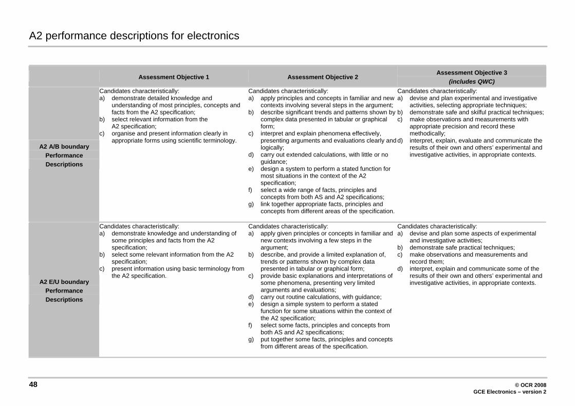
48 © OCR 2008 GCE Electronics – version 2
A2 performance descriptions for electronics
Assessment Objective 1 Assessment Objective 2 Assessment Objective 3
(includes QWC)
A2 A/B boundary Performance Descriptions
Candidates characteristically: a) demonstrate detailed knowledge and
understanding of most principles, concepts and facts from the A2 specification;
b) select relevant information from the A2 specification;
c) organise and present information clearly in appropriate forms using scientific terminology.
Candidates characteristically: a) apply principles and concepts in familiar and new
contexts involving several steps in the argument; b) describe significant trends and patterns shown by
complex data presented in tabular or graphical form;
c) interpret and explain phenomena effectively, presenting arguments and evaluations clearly and logically;
d) carry out extended calculations, with little or no guidance;
e) design a system to perform a stated function for most situations in the context of the A2 specification;
f) select a wide range of facts, principles and concepts from both AS and A2 specifications;
g) link together appropriate facts, principles and concepts from different areas of the specification.
Candidates characteristically: a) devise and plan experimental and investigative
activities, selecting appropriate techniques; b) demonstrate safe and skilful practical techniques; c) make observations and measurements with
appropriate precision and record these methodically;
d) interpret, explain, evaluate and communicate the results of their own and others’ experimental and investigative activities, in appropriate contexts.
A2 E/U boundary Performance Descriptions
Candidates characteristically: a) demonstrate knowledge and understanding of
some principles and facts from the A2 specification;
b) select some relevant information from the A2 specification;
c) present information using basic terminology from the A2 specification.
Candidates characteristically: a) apply given principles or concepts in familiar and
new contexts involving a few steps in the argument;
b) describe, and provide a limited explanation of, trends or patterns shown by complex data presented in tabular or graphical form;
c) provide basic explanations and interpretations of some phenomena, presenting very limited arguments and evaluations;
d) carry out routine calculations, with guidance; e) design a simple system to perform a stated
function for some situations within the context of the A2 specification;
f) select some facts, principles and concepts from both AS and A2 specifications;
g) put together some facts, principles and concepts from different areas of the specification.
Candidates characteristically: a) devise and plan some aspects of experimental
and investigative activities; b) demonstrate safe practical techniques; c) make observations and measurements and
record them; d) interpret, explain and communicate some of the
results of their own and others’ experimental and investigative activities, in appropriate contexts.

© OCR 2008 GCE Electronics – version 2 49
Appendix B: Coursework Assessment Criteria for AS Unit F613: Build and Investigate Electronic Circuits Analogue and Digital Circuits Section Criteria Marks
a described the circuit; 0–4 1. Introduction and Planning The candidate has: b explained the test procedure. 0–3
2. Circuit Realisation The candidate has:
a produced an organised and neat circuit build.
0–4
a shown evidence of a thorough testing programme;
0–3
b presented the results of the tests in an appropriate manner;
0–2
3. Testing and Analysis The candidate has:
c analysed the test results. 0–3 a included diagrams in the report to
support the written communication; 0–3
b produced a report that is well written; 0–3
4. The Report The candidate has:
c made good use of terminology. 0–2 Total /27 The table above gives an overview of the marking criteria for analogue and digital circuits; over the page is a more detailed breakdown of the marking criteria descriptors. The descriptors used give the highest attainment that would be expected of a candidate in that mark range.

50 © OCR 2008 GCE Electronics – version 2
Section Marks Digital/Analogue Circuit Descriptors 1a 0 The report does not contain a description of the circuit. 1–2 The report gives a possible use of the circuit and describes circuit
operation at a quantitative level. 3–4 The report describes circuit operation at a qualitative/quantitative
level and makes detailed predictions of expected outputs for a comprehensive set of inputs.
1b 0–1 The report identifies a basic test procedure that will produce at
least one set of input/output data. 2–3 The report identifies a test procedure that will produce data to
support detailed predictions made in 1a (three marks available only available if four marks have been awarded for 1a).
2a 0 The circuit build is haphazard and untidy. 1–2 The circuit has been built correctly and is very neat. 3–4 The circuit build is very neat and tidy, using an identifiable colour
code and meticulous wiring. 3a 0–2 The report contains evidence of a basic test procedure that has
produced a single set of input/output data that supports circuit operation at a qualitative level.
3 The report contains evidence of a thorough testing programme that supports the predictions made of expected outputs for a comprehensive set of inputs.
3b 0–1 The data of any basic test procedure has been presented in table
or graph form. 2 The data to support detailed circuit predictions made in 1a has
been presented in table or graph form (only available if three marks have been awarded for 3a).
3c 0–1 One or more sets of input/output data have been analysed to
support circuit operation. 2–3 Two or more sets of input/output have been analysed and a
detailed analysis of the predictions made in 1a has been carried out (three marks only available if four marks have been awarded for 1a).
4a 0–1 The report contains a correct circuit diagram. 2–3 The report also contains labelled diagrams that support the written
communication and also clearly show how the testing was performed.
4b 0–1 The report is easy to read and understand.
2–3 The report makes good use of spelling and grammar throughout
and the report is logically structured with appropriate headings. 4c 0 The terminology used in the report has been employed
inappropriately. 1–2 The report contains good use of terminology all of the time.

© OCR 2008 GCE Electronics – version 2 51
Microcontroller Circuits Section Criteria Marks
a described the circuit; 0–5 1. Introduction and Planning The candidate has: b explained the test procedure.
0–3
2. Circuit Realisation The candidate has:
a produced an organised and neat circuit build.
0–4
a shown evidence of a thorough testing programme;
0–3
b presented the results of the tests in an appropriate manner;
0–2
3. Testing and Analysis The candidate has:
c analysed the test results.
0–3
a included diagrams in the report to support the written communication;
0–2
b produced a report that is well written; 0–3
4. The Report The candidate has:
c made good use of terminology. 0–1 Total /26 The table above gives an overview of the marking criteria for microcontroller circuits; over the page is a more detailed breakdown of the marking criteria descriptors. The descriptors used give the highest attainment that would be expected of a candidate in that mark range.

52 © OCR 2008 GCE Electronics – version 2
Section Marks Microcontroller Circuit Descriptors 1a 0–1 The report contains a brief statement about circuit operation that
includes a possible use of the circuit. 2–3 The report contains a correct flowchart and describes circuit
operation at a qualitative level. 4–5 The report describes circuit operation at a quantitative level and
makes detailed predictions of expected outputs for a comprehensive set of inputs.
1b 0 The report does not contain any reference to the testing
procedure. 1–2 The report identifies a basic test procedure that will produce at
least one set of input/output data and a description of how the basic test procedure is to be carried out.
3 The report identifies a detailed test procedure that will produce data to support detailed predictions made in 1a (only available if five marks have been awarded for 1a).
2a 0 The circuit build does not merit a mark. 1–2 The circuit has been built correctly and is very neat. 3–4 The circuit build is very neat and tidy, using an identifiable colour
code and meticulous wiring. 3a 0–1 The report contains evidence of a basic test procedure that has
produced a single set of input/output data that supports circuit operation at a qualitative level.
2–3 The report contains evidence of a testing programme that produced a single set of input/output data and supports circuit operation at a quantitative level and predictions made of expected outputs for a comprehensive set of inputs.
3b 0 The presentation of results does not merit a mark. 1–2 The data to support detailed circuit predictions made in 1a has
been presented in an appropriate manner (two marks only available if three marks have been awarded for 3a).
3c 0–1 At least one set of input/output data has been analysed to
support circuit operation. 2–3 Two or more sets of input/output data have been analysed to
support circuit operation and a detailed analysis of the predictions made in 1a has been carried out (three marks only available if five marks have been awarded for 1a).
4a 0 No diagrams have been included in the report or the diagrams
presented do not merit a mark. 1–2 The report contains a correct circuit diagram, contains labelled
diagrams that support the written communication and clearly shows how the testing was performed.
4b 0–1 The report is easy to read and understand. 2–3 The report makes good use of spelling and grammar throughout
and the report is logically structured with appropriate headings. 4c 0–1 The report contains good use of terminology.

© OCR 2008 GCE Electronics – version 2 53
Appendix C: Suggested Investigations for AS Unit F613: Build and Investigate Electronic Circuits Digital Circuits
• A two-input multiplexer.
• A two-output demultiplexer.
• Any monostable circuit made from NAND/NOR gates.
• Any astable circuit made from NAND/NOR gates.
• Any relaxation oscillator circuit made with a Schmitt trigger NOT gate – frequency could be made variable by altering light intensity/temperature.
• A four-bit counter that resets on a given number – clock signal derived from signal generator.
Analogue Circuits
• A window detector.
• A treble cut filter with any reasonable gain.
• A bass cut filter with any reasonable gain.
• A summing amplifier used as a level shifter for any time-dependent signal – level shifting could be performed by a temperature dependent input, a light dependent input, etc.
• A summing amplifier circuit to mix two different ac signals.
• A comparator set up to provide a variable width square wave generator from a sinusoidal input; comparison voltage could be altered by temperature, light, etc.
• Any inverting/non-inverting amplifier circuit – gain–bandwidth product could be taken into account – input could be from an electret microphone.
• Any investigation into how closely the measured gain–bandwidth product for a real op-amp compares with the theoretical op-amp.
• A basic tone control circuit.
Microcontroller Circuits
• A simple 4-bit DAC, analogue input converted when a switched input is activated – output shown on a 7-segment display. Could be developed as a simple voltmeter.
• A counting circuit that counts square pulses from a signal generator. Circuit to use a switched input that could serve as an enable, followed by a choice of two ranges counted. With a 1 Hz input, could be developed as an egg timer. With faster pulses, could be developed as a stopwatch. Output to 7-segment display.
• Circuit to emulate a traffic light sequence.
• Circuit to create a ‘disco light effect’ from square pulses inputted from a signal generator. Output to a range of LEDs.
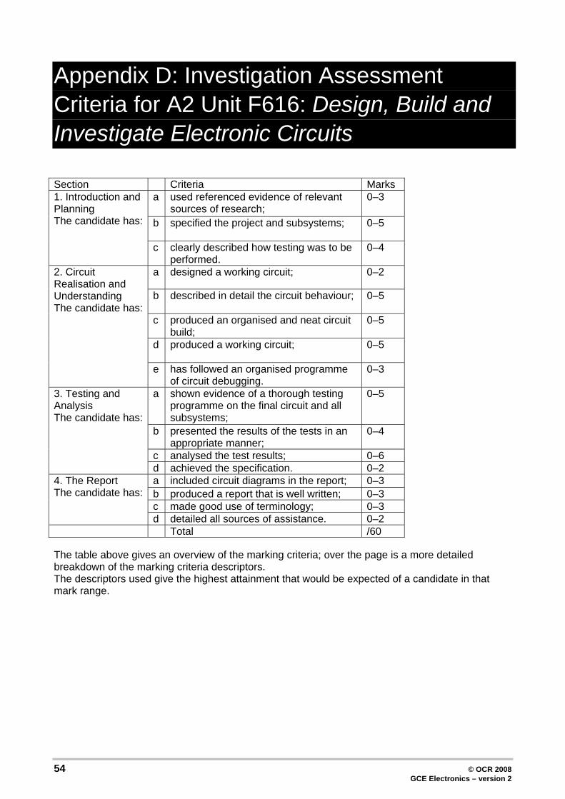
54 © OCR 2008 GCE Electronics – version 2
Appendix D: Investigation Assessment Criteria for A2 Unit F616: Design, Build and Investigate Electronic Circuits Section Criteria Marks
a used referenced evidence of relevant sources of research;
0–3
b specified the project and subsystems;
0–5
1. Introduction and Planning The candidate has:
c clearly described how testing was to be performed.
0–4
a designed a working circuit; 0–2
b described in detail the circuit behaviour; 0–5
c produced an organised and neat circuit build;
0–5
d produced a working circuit;
0–5
2. Circuit Realisation and Understanding The candidate has:
e has followed an organised programme of circuit debugging.
0–3
a shown evidence of a thorough testing programme on the final circuit and all subsystems;
0–5
b presented the results of the tests in an appropriate manner;
0–4
c analysed the test results; 0–6
3. Testing and Analysis The candidate has:
d achieved the specification. 0–2 a included circuit diagrams in the report; 0–3 b produced a report that is well written; 0–3 c made good use of terminology; 0–3
4. The Report The candidate has:
d detailed all sources of assistance. 0–2 Total /60 The table above gives an overview of the marking criteria; over the page is a more detailed breakdown of the marking criteria descriptors. The descriptors used give the highest attainment that would be expected of a candidate in that mark range.

© OCR 2008 GCE Electronics – version 2 55
Section Marks Descriptor 1a 0–1 The report contains limited relevant research to design the
project 2–3 The report refers in detail to relevant sources to design the
project. 1b 0 The project specification is too vague for its final evaluation. 1–2 The project has been specified in qualitative/quantitative terms. 3–5 The project and up to five subsystems have been specified in
qualitative and quantitative terms. 1c 0 The report contains no description of how testing was performed. 1–2 The report contains a clear description of the test procedure to be
carried out on the final circuit and at least one subsystem. 3–4 The report contains a clear description of the test procedure to be
carried out on the final circuit and up to five subsystems. 2a 0 The candidate designed at least one subsystem unaided. 1–2 The candidate designed up to three subsystems unaided and
needed little or no help in designing the entire project. 2b 0 The description of the project behaviour is vague and incomplete. 1–3 The candidate described project behaviour using a block diagram
approach; one subsystem has been correctly described at component level, with a correct calculation of a component value.
4–5 The entire project, including three or more subsystems, has been correctly described at component level.
2c 0 The project build is untidy with a haphazard layout of
components. 1–3 The project build shows evidence of a subsystem approach with
logical positioning and neat wiring.
4–5 The project build shows evidence of a subsystem approach with logical positioning, an identifiable colour code is used in which all wires are arranged vertically/horizontally with no unnecessary crossing of wires.
2d 0 No working subsystem was achieved. 1–3 Up to three working subsystems were built and tested. 4–5 The entire project worked (applicable to a project that contains up
to five subsystems). 2e 0 The candidate was unable to fault-find any subsystem unaided. 1–3 The candidate was able to fault-find up to five subsystems
unaided. 3a 0 The candidate did not present any evidence of testing on any
part of the project. 1–3 The report contains evidence of a test procedure and has
produced output data for a given set of input conditions applied to up to three subsystems.
4–5 The report contains evidence of a rigorous test procedure performed on the final project including five subsystems and has produced output data for the complete project in which two or more input variables have been used for all subsystems..
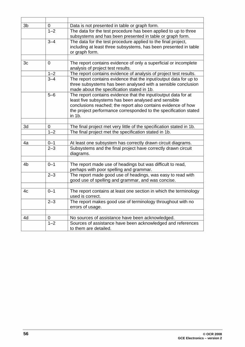
56 © OCR 2008 GCE Electronics – version 2
3b 0 Data is not presented in table or graph form. 1–2 The data for the test procedure has been applied to up to three
subsystems and has been presented in table or graph form. 3–4 The data for the test procedure applied to the final project,
including at least three subsystems, has been presented in table or graph form.
3c 0 The report contains evidence of only a superficial or incomplete
analysis of project test results. 1–2 The report contains evidence of analysis of project test results. 3–4 The report contains evidence that the input/output data for up to
three subsystems has been analysed with a sensible conclusion made about the specification stated in 1b.
5–6 The report contains evidence that the input/output data for at least five subsystems has been analysed and sensible conclusions reached; the report also contains evidence of how the project performance corresponded to the specification stated in 1b.
3d 0 The final project met very little of the specification stated in 1b. 1–2 The final project met the specification stated in 1b. 4a 0–1 At least one subsystem has correctly drawn circuit diagrams. 2–3 Subsystems and the final project have correctly drawn circuit
diagrams. 4b 0–1 The report made use of headings but was difficult to read,
perhaps with poor spelling and grammar. 2–3 The report made good use of headings, was easy to read with
good use of spelling and grammar, and was concise. 4c 0–1 The report contains at least one section in which the terminology
used is correct. 2–3 The report makes good use of terminology throughout with no
errors of usage. 4d 0 No sources of assistance have been acknowledged. 1–2 Sources of assistance have been acknowledged and references
to them are detailed.

© OCR 2008 GCE Electronics – version 2 57
Appendix E: Suggested Investigations for A2 Unit F616: Design, Build and Investigate Electronic Circuits • Pedometer, adjustable for stride length. Displays total distance covered, up to 999 m.
• Speed control of dc motor. Desired speed is set by keypad.
• Spectrum analyser for stereo system.
• Quizmaster with infrared controls.
• Radio remote control of professional VCR. System employs UART and microprocessor components. (Professional VCR is not normally remote-operated. Radio-transmission regulations must be observed).
• Delay and echo unit for electric guitar. Many variations have been offered.
• Ultrasonic tape measure. Achieving a range exceeding 1 m often provides a real challenge.
• ‘Cricket Master’, for umpires. It counts balls bowled and overs completed. Fits into the umpire’s pocket.
• Seven-day timer with two switch programmes per day. This battery-operated system could be adapted to control mains circuits but could be built and tested with low voltages.
• Solar tracker, using sensors and stepper motors to point the device at the Sun throughout the day.
• Digital speech sampler, using a microprocessor system to record a short sample of speech and play it back on demand.
• Door lock, operated by keypad. Use of microprocessor allows easy PIN change.
• Graphic equaliser with infrared remote control.
• Cricket scoreboard showing totals of runs and wickets. Runs are entered singly or as groups of 2, 3, 4, 5 or 6. The system could be in miniature, and battery-operated.
• Weather station data transmission system. Concentrating on digital transmission of analogue data, and subsequent checking and display. The collection of data is not part of the project.
• Stroboscope. A xenon tube was triggered at frequencies between 25 and 100 Hz. Xenon tubes need high voltages, and safety precautions need to be taken at each stage.
• Light-dimming device. It fades a lamp completely in 10 min. There are few applications, but the problem is unusual and challenging.
• High-speed data transmission. The system stores data over a period of time and loads it as one block rapidly into a computer.
• Multichannel lamp dimmer, controlling several lamps but using only one pair of wires.
• Lighting entertaining unit. The system modifies a light display in response to music. Three frequency bands are used.

58 © OCR 2008 GCE Electronics – version 2
• Anemometer recorder. Measures rotation speed of cogged ferrous wheel attached to the anemometer shaft and then converts to a wind speed, displayed in m s-1.
• Prototyping board with on-board regulated power supply, signal generator and debounced switches.

© OCR 2008 GCE Electronics – version 2 59
Appendix F: Formulae Relationships and Boolean Algebra
resistance IVR =
power VIP =
series resistors R = R1 + R2
time constant RC=τ
monostable pulse time T = 0.7RC
relaxation oscillator period T = 0.5RC
frequency T
f 1=
voltage gain
in
outVV
G =
open-loop op-amp Vout = A(V+ – V-)
non-inverting amplifier gain
d
fRR
G += 1
inverting amplifier gain
in
fRR
G −=
summing amplifier ...
2
2
1
1RV
RV
RV
f
out +=−
break frequency RC
fπ
=2
10
amplifier gain G = –gmRd
ramp generator
RCtVV inout
Δ−=Δ
inductor reactance fLXL π= 2

60 © OCR 2008 GCE Electronics – version 2
capacitor reactance
fCXC π
=2
1
resonant frequency
LCf
π=
21
0
Boolean Algebra
0AA. =
A.CA.BC)A.(B1AA
+=+=+
BAA.B += B.ABA =+
A + A.B = A
B.C.CAA.B.CAA.B ++=+

© OCR 2008 GCE Electronics – version 2 61
Appendix G: Microcontroller flowchart symbols Candidates should be able to use these flowchart symbols to analyse and synthesise a microcontroller with an eight-bit input port, an eight-bit output port, an analogue-to-digital converter and a set of registers An, where n = 0, 1, 2 ... All bytes are written in hexadecimal notation. For example F2 is the byte 1111 0010.
Control
symbol meaning
start the program
link to part of the program with the same label a
stop the program
Process symbol meaning
place the byte b in register An
add the byte b to the byte in register An
copy the byte in register Am into register An
subtract the byte b from the byte in register An
introduce a time delay of t milliseconds
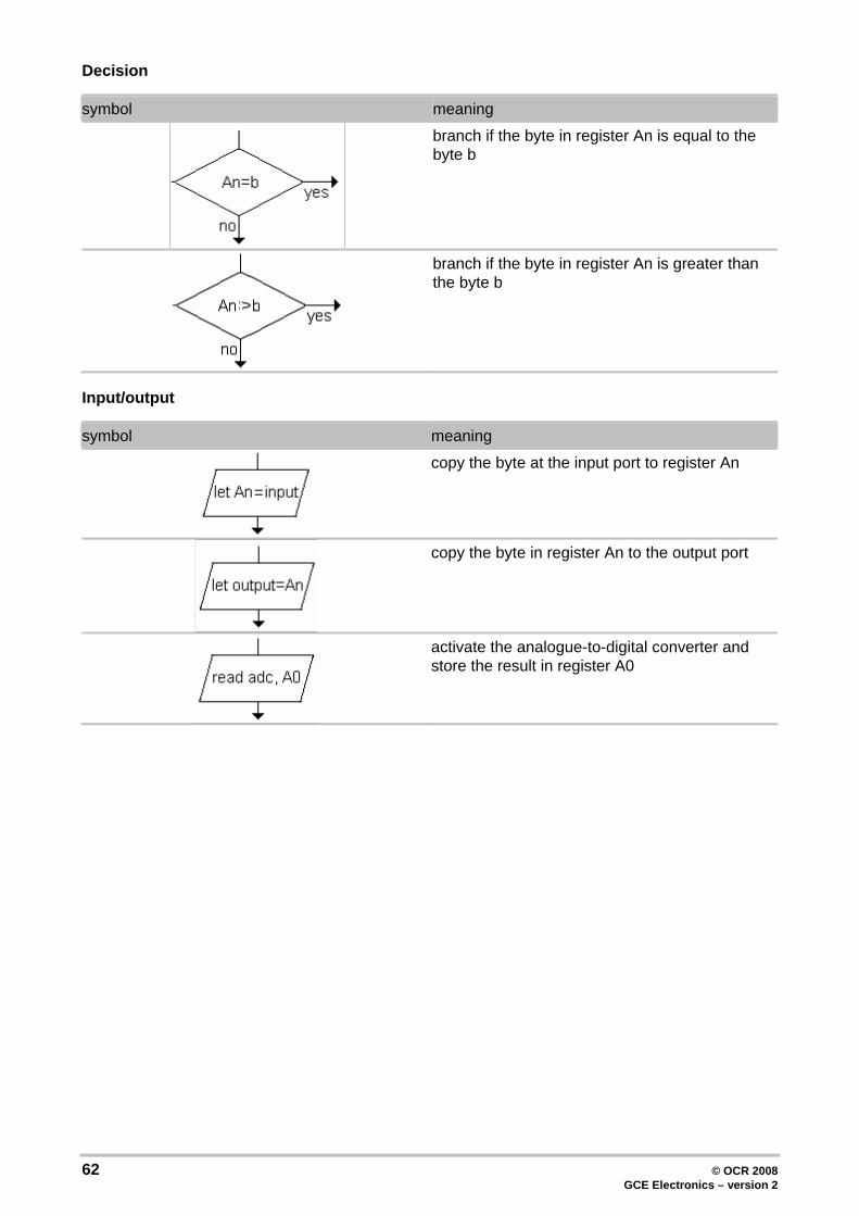
62 © OCR 2008 GCE Electronics – version 2
Decision
symbol meaning
branch if the byte in register An is equal to the byte b
branch if the byte in register An is greater than the byte b
Input/output
symbol meaning
copy the byte at the input port to register An
copy the byte in register An to the output port
activate the analogue-to-digital converter and store the result in register A0
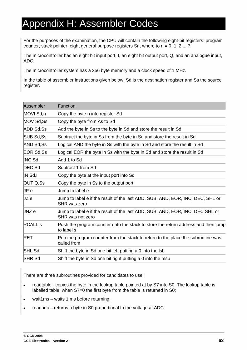
© OCR 2008 GCE Electronics – version 2 63
Appendix H: Assembler Codes For the purposes of the examination, the CPU will contain the following eight-bit registers: program counter, stack pointer, eight general purpose registers Sn, where to n = 0, 1, 2 ... 7.
The microcontroller has an eight bit input port, I, an eight bit output port, Q, and an analogue input, ADC.
The microcontroller system has a 256 byte memory and a clock speed of 1 MHz.
In the table of assembler instructions given below, Sd is the destination register and Ss the source register.
Assembler Function
MOVI Sd,n Copy the byte n into register Sd
MOV Sd,Ss Copy the byte from As to Sd
ADD Sd,Ss Add the byte in Ss to the byte in Sd and store the result in Sd
SUB Sd,Ss Subtract the byte in Ss from the byte in Sd and store the result in Sd
AND Sd,Ss Logical AND the byte in Ss with the byte in Sd and store the result in Sd
EOR Sd,Ss Logical EOR the byte in Ss with the byte in Sd and store the result in Sd
INC Sd Add 1 to Sd
DEC Sd Subtract 1 from Sd
IN Sd,I Copy the byte at the input port into Sd
OUT Q,Ss Copy the byte in Ss to the output port
JP e Jump to label e
JZ e Jump to label e if the result of the last ADD, SUB, AND, EOR, INC, DEC, SHL or SHR was zero
JNZ e Jump to label e if the result of the last ADD, SUB, AND, EOR, INC, DEC SHL or SHR was not zero
RCALL s Push the program counter onto the stack to store the return address and then jump to label s
RET Pop the program counter from the stack to return to the place the subroutine was called from
SHL Sd Shift the byte in Sd one bit left putting a 0 into the lsb
SHR Sd Shift the byte in Sd one bit right putting a 0 into the msb
There are three subroutines provided for candidates to use:
• readtable - copies the byte in the lookup table pointed at by S7 into S0. The lookup table is labelled table: when S7=0 the first byte from the table is returned in S0;
• wait1ms – waits 1 ms before returning;
• readadc – returns a byte in S0 proportional to the voltage at ADC.

64 © OCR 2008 GCE Electronics – version 2
Appendix I: Standard Circuit Symbols This document clarifies the range of symbols that will be used in OCR GCE Electronics. They form a minimum set of symbols with which candidates must be familiar. As part of their studies, it is expected that candidates will use a range of source materials and should therefore be aware that a wider range of symbols is in actual use and that variations may be found.
AND OR NAND
TERMINAL
CELL FUSESPEAKER
MICROPHONE
CAPACITORELECTROLYTIC CAPACITOR
PRESETCAPACITOR
VARIABLECAPACITOR
DC SUPPLY AC SUPPLY
JUNCTION OFCONDUCTORS
DOUBLE JUNCTIONOF CONDUCTORS
BUZZER
M
MOTOR
G A
GENERATOR AMMETER
M
STEPPER MOTOR
PUSH SWITCH AIR CORED INDUCTOR
OP AMP
SPST SWITCH DPDT SWITCH
LED ZENER DIODE
NPNTRANSISTOR
PNPTRANSISTOR
DIODE

© OCR 2008 GCE Electronics – version 2 65
INDUCTOR TRANSFORMER AERIAL EARTH HEATER
XOR NOTNOR
CONDUCTORS CROSSING COUNTER
A B
CK
RESISTOR PRESET RESISTOR VARIABLE RESISTOR
POTENTIOMETER
VOLTMETER
V
OSCILLOSCOPE LAMP MAKE CONTACTRELAY COIL
PHOTO - DIODED TYPE TRISTATESCHMITTINVERTER
D Q
Q
N - MOSFET TRIAC OPTO - COUPLERTHERMISTOR
LDR
R