Embed Size (px)
Citation preview

ASICs...THE COURSE (1 WEEK)
1
ASIC LIBRARY DESIGN
ASIC design uses predefined and precharacterized cells from a library—so we need todesign or buy a cell library. A knowledge of ASIC library design is not necessary but makesit easier to use library cells effectively.
3.1 Transistors as Resistors
Key concepts: Tau, logical effort, and the prediction of delay • Sizes of cells, and their drive
strengths • Cell importance • The difference between gate-array macros, standard cells, and
datapath cells
–tPDf
0.35VDD = VDD exp –––––––––––––––––
Rpd (Cout + Cp)
An output trip point of 0.35 is convenient because ln(1/0.35)=1.04≈1 and thus
tPDf = Rpd(Cout + Cp) ln (1/0.35) ≈ Rpd(Cout + Cp)
For output trip points of 0.1/0.9 we multiply by –ln(0.1) = 2.3, because exp (–2.3) = 0.100
3

2 SECTION 3 ASIC LIBRARY DESIGN ASICS... THE COURSE
A linear model for CMOS logic delay
• Ideal switches = no delay • Resistance and capacitance causes delay
• Load capacitance, Cout • parasitic output capacitance, Cp • input capacitance, C
• Linearize the switch resistance • Pull-up resistance, Rpu • pull-down resistance, Rpd
• Measure and compare the input, v(in1) and output, v(out1)
• Input trip point of 0.5 • output trip points are 0.35 (falling) and 0.65 (rising)
• The linear prop–ramp model: falling propagation delay, tPDf ≈Rpd(Cp+Cout)
(c)
Rpu
Rpd
Cp
VDD
in1 out1
CoutC
(a)
VDD
in1 out1
Cout
m1
m2
v(in1)v(out1)
tPDf
VDD
0.5VDD
0.35VDD
saturation linearoff
0
(b)
t'
m2
m1
m1:t' =0
t' =0 ≈ Rpd (Cp + Cout)
VDD exp[–t' / (Rpd (Cp + Cout))]
t' =0
–IDSp
IDSn–(IDSp + IDSn)

ASICs... THE COURSE 3.1 Transistors as Resistors 3
(a) (b)
CMOS inverter characteristics
• Equilibrium switching
• Non-equilibrium switching
• Nonlinear switching resistance
• Switching current
(c)
v(in1) /V
v(out1) / V
0
1
2
3
1 2 30
equilibriumpath
nonequilibrium path
IDSn=–IDSp
1
0
3
1
23
0
3
2
0
1
v(in1) /V
v(out1) / V
nonequilibrium pathmax(IDSn, –IDSp) /mA
IDSn
–IDSp
1
2
equilibriumpath
v(in1) /V
0.2
0.4
0.01 2 30
equilibriumpath
2
IDSn=–I DSp
max(IDSn, –IDSp) /mA

4 SECTION 3 ASIC LIBRARY DESIGN ASICS... THE COURSE
3.2 Transistor Parasitic Capacitance
Transistor parasitic capacitance
• Constant overlap capacitances CGSOV, CGDOV, and CGBOV
• Variable capacitances CGS, CGB, and CGD depend on the operating region
• CBS and CBD are the sum of the area (CBSJ, CBDJ), sidewall (CBSSW, CBDSW), and chan-nel edge (CBSJGATE, CBDJGATE) capacitances
• LD is the lateral diffusion • TFOX is the field-oxide thickness
(d)
D
S
G
CGDOV
CGSOV
B
CBD= CBDJ + CBDSW+ CBDJGATE
CGB
(c)
G
D
S
W
L
TFOX
(b)
(e) (f) (h)
WEFFLEFF
Tox
ndiff
poly
(a)
W
L
S
G
D
CGBOV
CGD
CGS
CBS= CBSJ + CBSSW+ CBSJGATE
S
LD
1
CBSSW
CGS
CGB
CGD
CGBOV
CGDOV
CGSOV(g)
S
CBSJ
poly
pwell
ASPS
AS
PS
channeledge
channel edge
channel edge
3
2 5
3
1
4
5
2 5
3
3
4
45
1
WEFF
LEFF
CBSJ GATE
channel edge
1
3
2
2CBDSW
CGB
CGDOV
CGD
D
G
channel
depletion region
S
CBSJ CBDJ4 4
CGSOVCBSSW
CGS1
2
3
bulk, B
GND orVSS
LDD diffusionfieldimplant
FOX

ASICs... THE COURSE 3.2 Transistor Parasitic Capacitance 5
NAME m1 m2 MODEL CMOSN CMOSP ID 7.49E-11 -7.49E-11VGS 0.00E+00 -3.00E+00VDS 3.00E+00 -4.40E-08VBS 0.00E+00 0.00E+00VTH 4.14E-01 -8.96E-01VDSAT 3.51E-02 -1.78E+00GM 1.75E-09 2.52E-11GDS 1.24E-10 1.72E-03GMB 6.02E-10 7.02E-12CBD 2.06E-15 1.71E-14CBS 4.45E-15 1.71E-14CGSOV 1.80E-15 2.88E-15CGDOV 1.80E-15 2.88E-15CGBOV 2.00E-16 2.01E-16CGS 0.00E+00 1.10E-14CGD 0.00E+00 1.10E-14CGB 3.88E-15 0.00E+00
• ID (IDS), VGS, VDS, VBS, VTH (Vt), and VDSAT (VDS(sat)) are DC parameters
• GM, GDS, and GMB are small-signal conductances (corresponding to ∂IDS/∂VGS,∂IDS/∂VDS, and ∂IDS/∂VBS, respectively)

6 SECTION 3 ASIC LIBRARY DESIGN ASICS... THE COURSE

ASICs... THE COURSE 3.2 Transistor Parasitic Capacitance 7
Calculations of parasitic capacitances for an n-channel MOS transistor.
PSpice Equation Values1 for VGS=0V, VDS=3V, VSB=0V
CBD
CBD = CBDJ + CBDSW
CBD = 1.855 × 10⁻¹³ + 2.04 × 10–16 = 2.06 ×
10–13 F
CBDJ + AD CJ ( 1 + VDB/φB)–mJ (φB = PB)
CBDJ = (4.032 × 10⁻¹⁵)(1 + (3/1))–0.56 = 1.86 ×
10–15 F
CBDSW = PD CJSW (1 + VDB/φB)–mJSW (PD may or may not include channel edge)
CBDSW = (4.2 × 10⁻¹⁶)(1 + (3/1))–0.5 = 2.04 ×
10–16 F
CBS
CBS = CBSJ + CBSSW
CBS = 4.032 × 10⁻¹⁵ + 4.2 × 10–16 = 4.45 ×
10–15 F
CBSJ + AS CJ ( 1 + VSB/φB)–mJAS CJ = (7.2 × 10⁻¹⁵)(5.6 × 10⁻⁴) = 4.03 ×
10–15 F
CBSSW = PS CJSW (1 + VSB/φB)–mJSWPS CJSW = (8.4 × 10⁻⁶)(5 × 10–11) = 4.2 ×
10–16 F
CGSOV CGSOV=WEFFCGSO ; WEFF=W–2WD CGSOV = (6 × 10⁻⁶)(3 × 10⁻¹⁰) = 1.8 × 10⁻¹⁶ F
CGDOV CGDOV=WEFFCGSO CGDOV = (6 × 10⁻⁶)(3 × 10⁻¹⁰) = 1.8 × 10⁻¹⁵ F
CGBOV CGBOV=LEFFCGBO ; LEFF=L–2LD CGDOV = (0.5 × 10⁻⁶)(4 × 10⁻¹⁰) = 2 × 10–16 F
CGS CGS/CO = 0 (off), 0.5 (lin.), 0.66 (sat.)CO (oxide capacitance) = WEF LEFF εox / Tox
CO = (6 × 10⁻⁶)(0.5 × 10⁻⁶)(0.00345) = 1.03 ×
10–14 FCGS = 0.0 F
CGD CGD/CO = 0 (off), 0.5 (lin.), 0 (sat.) CGD = 0.0 F
CGB CGB = 0 (on), = CO in series with CGS (off)
CGB = 3.88 × 10⁻¹⁵ F, CS=depletion capaci-tance
1Input .MODEL CMOSN NMOS LEVEL=3 PHI=0.7 TOX=10E-09 XJ=0.2U TPG=1 VTO=0.65 DELTA=0.7+ LD=5E-08 KP=2E-04 UO=550 THETA=0.27 RSH=2 GAMMA=0.6 NSUB=1.4E+17 NFS=6E+11+ VMAX=2E+05 ETA=3.7E-02 KAPPA=2.9E-02 CGDO=3.0E-10 CGSO=3.0E-10 CGBO=4.0E-10+ CJ=5.6E-04 MJ=0.56 CJSW=5E-11 MJSW=0.52 PB=1m1 out1 in1 0 0 cmosn W=6U L=0.6U AS=7.2P AD=7.2P PS=8.4U PD=8.4U

8 SECTION 3 ASIC LIBRARY DESIGN ASICS... THE COURSE
3.2.1 Junction Capacitance
• Junction capacitances, CBD and CBS, consist of two parts: junction area and sidewall
• Both CBD and CBS have different physical characteristics with parameters: CJ and MJ for the junction, CJSW and MJSW for the sidewall, and PB is common
• CBD and CBS depend on the voltage across the junction (VDB and VSB)
• The sidewalls facing the channel (CBSJGATE and CBDJGATE) are different from the side-walls that face the field
• It is a mistake to exclude the gate edge assuming it is in the rest of the model—it is not
• In HSPICE there is a separate mechanism to account for the channel edge capaci-tance (using parameters ACM and CJGATE)
3.2.2 Overlap Capacitance
• The overlap capacitance calculations for CGSOV and CGDOV account for lateral diffusion
• SPICE parameter LD=5E-08 or LD=0.05µm
• Not all SPICE versions use the equivalent parameter for width reduction, WD, in calcu-lating CGDOV
• Not all SPICE versions subtract WD to form WEFF
3.2.3 Gate Capacitance
• The gate capacitance depends on the operating region
• The gate–source capacitance CGS varies from zero (off) to 0.5CO in the linear region to(2/3)CO in the saturation region
• The gate–drain capacitance CGD varies from zero (off) to 0.5CO (linear region) andback to zero (saturation region)
• The gate–bulk capacitance CGB is two capacitors in series: the fixed gate-oxide capaci-tance, CO, and the variable depletion capacitance, CS
• As the transistor turns on the channel shields the bulk from the gate—and CGB falls tozero
• Even with VGS=0V, the depletion width under the gate is finite and thus CGB is less thanCO

ASICs... THE COURSE 3.2 Transistor Parasitic Capacitance 9
The variation of n-channel transistor parasitic capacitance
• PSpice v5.4 (LEVEL=3)
• Created by varying the input voltage, v(in1), of an inverter
• Data points are joined by straight lines
• Note that CGSOV=CGDOV
0
2
4
6
0 0.5 1 1.5 2 2.5 3
CBD CBS CGSOV CGDOV
CGBOV CGS CGD CGB
capacitance/fF
inverter input voltage, v(in1) /V
off saturation linear
10 SECTION 3 ASIC LIBRARY DESIGN ASICS... THE COURSE
3.2.4 Input Slew Rate
(a)
(b)
(c)
Measuring the input capacitance of an inverter
(a) Input capacitance is measured by monitoring the input current to the inverter, i(Vin)
(b) Very fast (non-equilibrium) switching: input current of 40fA = input capacitance of 40fF
(c) Very slow (equilibrium) switching: input capacitance is now equal for both transitions

ASICs... THE COURSE 3.2 Transistor Parasitic Capacitance 11
(a) (c)
(b)(d)
Parasitic capacitance measurement
(a) All devices in this circuit include parasitic capacitance
(b) This circuit uses linear capacitors to model the parasitic capacitance of m9/10.
• The load formed by the inverter (m5 and m6) is modeled by a 0.0335pF capacitor (c2)
• The parasitic capacitance due to the overlap of the gates of m3 and m4 with their source, drain, and bulk terminals is modeled by a 0.01pF capacitor (c3)
• The effect of the parasitic capacitance at the drain terminals of m3 and m4 is modeled by a 0.025pF capacitor (c4)
(c) Comparison of (a) and (b). The delay (1.22–1.135=0.085ns) is equal to tPDf for the in-verter m3/4
(d) An exact match would have both waveforms equal at the 0.35 trip point (1.05V).

12 SECTION 3 ASIC LIBRARY DESIGN ASICS... THE COURSE
3.3 Logical Effort
We extend the prop–ramp model with a “catch all” term, tq, that includes:
• delay due to internal parasitic capacitance
• the time for the input to reach the switching threshold of the cell
• the dependence of the delay on the slew rate of the input waveform
• R and C will change as we scale a logic cell, but the RC product stays the same
• Logical effort is independent of the size of a logic cell
• We can find logical effort by scaling a logic cell to have the same drive as a 1Xminimum-size inverter
• Then the logical effort, g, is the ratio of the input capacitance, Cin, of the 1X logic cell toCinv
tPD = R(Cout + Cp) + tqWe can scale any logic cell by a scaling factor s: tPD = (R/s)·(Cout + sCp) + stq
Cout
tPD = RC –––––– + RCp + stq
Cin
(RC) (Cout / Cin ) + RCp + stq
Normalizing the delay: d = ––––––––––––––––––––––––––––––– = f + p + q
τ
The time constant tau, τ = Rinv Cinv , is a basic property of any CMOS technology
The delay equation is the sum of three terms, d = f + p + q or delay = effort delay + parasitic delay + nonideal delay
The effort delay f is the product of logical effort, g, and electrical effort, h: f = gh
Thus, delay = logical effort × electrical effort + parasitic delay + nonideal delay
ASICs... THE COURSE 3.3 Logical Effort 13
The h depends only on the load capacitance Cout connected to the output of the logiccell and the input capacitance of the logic cell, Cin; thus
Logical effort • For a two-input NAND cell, the logical effort, g=4/3
(a) Find the input capacitance, Cinv, looking into the input of a minimum-size inverter in terms of the gate capacitance of a minimum-size device
(b) Size a logic cell to have the same drive strength as a minimum-size inverter (assuming a logic ratio of 2). The input capacitance looking into one of the logic-cell terminals is then Cin
(c) The logical effort of a cell is Cin/ Cinv
electrical effort h = Cout /Cin
parasitic delay p = RCp/τ (the parasitic delay of a minimum-size inverter is: pinv = Cp/ Cinv )
nonideal delay q = stq /τ
Cell effort, parasitic delay, and nonideal delay (in units of τ) for single-stage CMOS cells
Cell Cell effort(logic ratio=2)
Cell effort(logic ratio=r) Parasitic delay/τ Nonideal delay/τ
inverter 1 (by definition) 1 (by definition) pinv (by definition) qinv (by definition)
n-input NAND (n+2)/3 (n+r)/(r+1) npinv nqinv
n-input NOR (2n+1)/3 (nr+1)/(r+1) npinv nqinv
(b)
Cin =2+2=4
Measure the inputcapacitance of aminimum-sizeinverter.
Make the cell have the samedrive strength as aminimum-size inverter.
g = C in/Cinv= 4/3
1X
2/1
2/1
2/1 2/1
(a)
2/1
1/1
2 units ofgate capacitance
1 unitCinv
1X
Cinv
(c)
Cinv =2+1=3
A
A
Measure ratio of cell inputcapacitance to that of aminimum-size inverter.
1
2 3
ZNZN

14 SECTION 3 ASIC LIBRARY DESIGN ASICS... THE COURSE
3.3.1 Predicting Delay
• Example: predict the delay of a three-input NOR logic cell
• 2X drive
• driving a net with a fanout of four
• 0.3pF total load capacitance (input capacitance of cells we are driving plus the inter-connect)
• p=3pinv and q=3qinv for this cell
• the input gate capacitance of a 1X drive, three-input NOR logic cell is equal to gCinv
• for a 2X logic cell, Cin = 2gCinv
The delay of the NOR logic cell, in units of τ, is thus
Cout g·(0.3 pF) (0.3 pF)
gh = g ––––– = ––––––––––– = –––––––––––– (Notice g cancels out in this equation)
Cin 2gCinv (2)·(0.036 pF)
0.3 × 10⁻¹²
d = gh + p + q = –––––––––––––––––––– + (3)·(1) + (3)·(1.7)
(2)·(0.036 × 10–12)
= 4.1666667 + 3 + 5.1
= 12.266667 τ equivalent to an absolute delay, tPD≈12.3 ×0.06ns=0.74ns
The delay for a 2X drive, three-input NOR logic cell is tPD = (0.03 + 0.72Cout + 0.60) ns
With Cout=0.3pF, tPD = 0.03 + (0.72)·(0.3) + 0.60 = 0.846 ns compared to our prediction of0.74ns

ASICs... THE COURSE 3.3 Logical Effort 15
3.3.2 Logical Area and Logical Efficiency
An OAI221 logic cell
• Logical-effort vector g=(7/3, 7/3, 5/3)
• The logical area is 33 logical squares
An AOI221 logic cell
• g=(8/3, 8/3, 7/3)
• Logical area is 39 logical squares
• Less logically efficient than OAI221
Z
4/1 4/1
4/14/1
A
B
C
D
VDD
2/1E
3/1A
3/1C
3/1B
3/1D
Z
ABCDE 3/1
E
VDD
Z
6/1 6/1
6/16/1
6/1
A
C
E
B
D
1/1E
2/1A
2/1B
2/1C
2/1D
Z
ABCDE
16 SECTION 3 ASIC LIBRARY DESIGN ASICS... THE COURSE
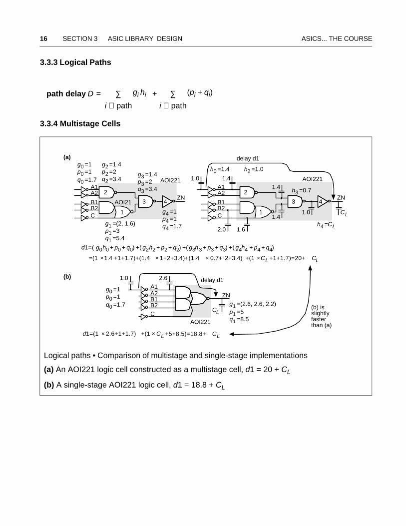
3.3.3 Logical Paths
3.3.4 Multistage Cells
path delay D = ∑ gi hi + ∑ (pi + qi)
i ∈ path i ∈ path
Logical paths • Comparison of multistage and single-stage implementations
(a) An AOI221 logic cell constructed as a multistage cell, d1 = 20 + CL
(b) A single-stage AOI221 logic cell, d1 = 18.8 + CL
(a)
(b)
d1=(1 × 2.6+1+1.7) +(1 × CL +5+8.5)=18.8+ CL
d1=( g0h0 + p0 + q0) +( g2h2 + p2 + q2) +( g3h3 + p3 + q3) +( g4h4 + p4 + q4)
=(1 ×1.4 +1+1.7)+(1.4 × 1+2+3.4)+(1.4 × 0.7+ 2+3.4) +(1 ×CL +1+1.7)=20+ CL
AOI21
g4 =1p4 =1q4 =1.7
ZN
C
A1A2
B1B2
ZN
1.01.4
1.41.0
2.0 1.6
CLC
A1A2
B1B2
g1 =(2, 1.6)p1 =3q1 =5.4
g0 =1p0 =1q0 =1.7
g2 =1.4p2 =2q2 =3.4
delay d1
g3 =1.4p3 =2q3 =3.4
ZN
C
A1A2B1B2
AOI221
2.6
g0 =1p0 =1q0 =1.7 g1 =(2.6, 2.6, 2.2)
p1 =5q1 =8.5
CL
delay d1
h0 =1.4
1.4
h3 =0.7
h4 =CL
2
1
3 4 43
1
2
AOI221 AOI221
1.0
(b) isslightlyfasterthan (a)
h2 =1.0

ASICs... THE COURSE 3.3 Logical Effort 17
3.3.5 Optimum Delay
3.3.6 Optimum Number of Stages
• Chain of N inverters each with equal stage effort, f=gh
• Total path delay is Nf=Ngh=Nh, since g=1 for an inverter
path logical effort G = ∏ gi
i ∈ path
Cout
path electrical effort H = ∏ hi –––––
i ∈ path Cin
Cout is the load and Cin is the first input capacitance on the path
path effort F = GH
optimum effort delay f^i = gihi = F1/N
optimum path delay D^ = NF1/N = N(GH)1/N + P + Q
P + Q = ∑ pi + hi
i ∈ path
Stage effort
h h/(ln h)
1.5 3.7
2 2.9
2.7 2.7
3 2.7
4 2.9
5 3.1
10 4.3
0
2
4
6
8
10
12
1 2 3 4 5 6 7 8 9 10
= h /(ln h)
stage electrical effort, h=H 1/N
Delay of N inverter stages drivinga path effort of H = Cout /Cin.
Cin Cout
1 N2
h
delay/(ln H)
h

18 SECTION 3 ASIC LIBRARY DESIGN ASICS... THE COURSE
• To drive a path electrical effort H, hN=H, or N lnh=lnH
• Delay, Nh = hlnH/lnh
• Since lnH is fixed, we can only vary h/ln(h)
• h/ln(h) is a shallow function with a minimum at h=e ≈2.718
• Total delay is Ne=eln H
3.4 Library-Cell Design
• A big problem in library design is dealing with design rules
• Sometimes we can waive design rules
• Symbolic layout, sticks or logs can decrease the library design time (9 months forVirtual Silicon–currently the most sophisticated standard-cell library)
• Mapping symbolic layout uses 10–20 percent more area (5–10 percent with compac-tion)
• Allowing 45° layout decreases silicon area (some companies do not allow 45° layout)

ASICs... THE COURSE 3.5 Library Architecture 19
3.5 Library Architecture
(a) (b)
(c) (d)
Cell library statistics
• 80percent of an ASIC uses less than 20percent of the cell library
• Cell importance
• A D flip-flop (with a cell importance of 3.5) contributes 3.5 times as much area on a typi-cal ASIC than does an inverter (with a cell im-portance of 1)
(e)
cell numberordered bycell use
normalized cell use(minimum-size inverter=1)
0
1
cell numberordered bycell use
50 normalized cell area(minimum-size inverter=1)
0
cell area × cell use(minimum-size inverter=1)
cell numberordered bycell use
0
4
0
1
cell numberordered bycell importance
normalized cell importance(D flip-flop=1)
cell importance =cell area × cell use(D flip-flop=1)
cell use (minimum-size inverter=1)
0
1
cell numberordered bycell use andby cell importance

20 SECTION 3 ASIC LIBRARY DESIGN ASICS... THE COURSE
3.6 Gate-Array Design
Key words: gate-array base cell (or base cell) • gate-array base (or base) • horizontal tracks •
vertical track • gate isolation • isolator transistor • oxide isolation • oxide-isolated gate array
The construction of a gate-isolated gate array
(a) The one-track-wide base cell containing one p-channel and one n-channel transistor
(b) The center base cell is isolating the base cells on either side from each other
(c) The base cell is 21 tracks high (high for a modern cell library)
n-well
p-well
n-diff
p-diff
poly
m1
m2
contact
(a) (b) (c)
continuousp-diff strip
continuousn-diff strip
VDD
VSS
n-wellcontact
p-wellcontact
bent gate
1
2
3
4
5
6
7
8
9
10
11
12
13
14
15
16
17
18
19
20
21
contact forisolator

ASICs... THE COURSE 3.6 Gate-Array Design 21
An oxide-isolated gate-array base cell
• Two base cells, each contains eight transistors and two well contacts
• The p-channel and n-channel transistors are each 4 tracks high
• The cell is 12 tracks high (8–12 is typical for a modern library)
• The base cell is 7 tracks wide
VDD
GND
n-wellp-welln-diff
p-diffpoly
m1m2contact
n-wellcontactp-wellcontact
base cell
break in diffusion
12
(3)
45
6
7
89
(10)
11
12
1 2 3 4 5 6 7poly
p-diff
n-diff
p-diff

22 SECTION 3 ASIC LIBRARY DESIGN ASICS... THE COURSE
An oxide-isolated gate-array base cell
• 14 tracks high and 4 tracks wide
• VDD (tracks 3 and 4) and GND (tracks 11 and 12) are each 2 tracks wide
• 10 horizontal routing tracks (tracks 1, 2, 5–10, 13, 14)—unusually large number for mod-ern cells
• p-channel and n-channel polysilicon bent gates are tied together in the center of the cell
• The well contacts leave room for a poly cross-under in each base cell.
n-well
p-well
n-diff
p-diff
poly
m1
m2
contact
poly cross-under
VDD
VSS
1
2
(3)
(4)
5
6
7
8
9
10
(11)
(12)
13
14
n-well contact
1 2 3 4

ASICs... THE COURSE 3.6 Gate-Array Design 23
Flip-flop macro in a gate-isolated gate-array library
• Only the first-level metallization and contact pattern, the personalization, is shown, but this is enough information to derive the schematic
• This is an older topology for 2LM (cells for 3LM are shorter in height)
D
Q
contact forisolator
VDD
VSS
connector
CLR
QN
CLK

24 SECTION 3 ASIC LIBRARY DESIGN ASICS... THE COURSE
The SiARC/Synopsys cell-based array (CBA) basic cell
• This is CBA I for 2LM (CBA II is intended for 3LM and salicide proceses)
n-well
p-well
n-diff
p-diff
poly
m1
m2
1
2
3
4
5
6
7
8
9
10
11

ASICs... THE COURSE 3.6 Gate-Array Design 25
A simple gate-array base cell
aa bb cc dd ee ff gg hh ii jj kk ll
ab
c
def
g
hi
j
k
l
m
n
o
p
q
mm
nn
oo
xx
yy
aa+bb
= 2.75= (0.5 × P.4 + C.3)
= 1.25= 0.5 × P.4
= xx + yy
= 1.5= C.3
n-well
poly
ndiff
contact
ndiff pdiff
pdiff
BB
BB BB
basecell 1
basecell 2
BB = cell bounding box
p-well

26 SECTION 3 ASIC LIBRARY DESIGN ASICS... THE COURSE
3.7 Standard-Cell Design
A D flip-flop standard cell
• Performance-optimized library • Area-optimized library
• Wide power buses and transistors for a performance-optimized cell
• Double-entry cell intended for a 2LM process and channel routing
• Five connectors run vertically through the cell on m2
• The extra short vertical metal line is an internal crossover
• bounding box (BB) • abutment box (AB) • physical connector • abut

ASICs... THE COURSE 3.7 Standard-Cell Design 27
A D flip-flop from a 1.0µm standard-cell library
VDD
GND

28 SECTION 3 ASIC LIBRARY DESIGN ASICS... THE COURSE
D flip-flop
(Top) n-diffusion, p-diffusion, poly, contact (n-well and p-well are not shown)
(Bottom) m1, contact, m2, and via layers
poly
ndiff
pdiff
contactt1 t2 t3
t4 t5t6 t7 t8
t9 t10 t11
t12 t13
t14 t15
t20 t21t22
t23
t24
t25 t26 t27
t28
t29t30
t31
t32
t33
t34
1 1
1
1 1 1 1
00
00
2
2
3
3
3
44
4
5
5
5 5
6
6
6 6
6
7
7
7
7
8
8
8
9
9
9
10
10
10
c
d
d
a
b
b
e
e
10
9
10
via
m1
m2
contactVDD
VSS
ba
1
0
2 3
4 5
5 5
35
6
67
7
8
9
10
c
d6
8
c d e

ASICs... THE COURSE 3.8 Datapath-Cell Design 29
3.8 Datapath-Cell Design
A datapath D flip-flop cell
VDD
VDD
VSS
VSS

30 SECTION 3 ASIC LIBRARY DESIGN ASICS... THE COURSE
The schematic of a datapath D flip-flop cell
A narrow datapath
(a) Implemented in a two-level metal process
(b) Implemented in a three-level metal pro-cess
(a)
(b)
VDD
t8
t7
p1
n1
8/1.8
6/1.8
Dp2
n2
6/1.8
10/1.8t6
t3n1
n1
p1
t5
t4
p1
n1
10/1.8
6/1.8
t10
t9
p1
n1
4.5/13.6
4.5/6.7
t16
t15
p1
n1
8/1.8
6/1.8
t18
t17
p1
n1
4.5/13.6
4.5/6.7
p2
n2
6/1.8
10/1.8t14
t11n1
p1
t13
t12
p1
n1
10/1.8
6/1.8
VSS
t20
t19
p1
n1
8/1.8
6/1.8
t2
t1
p1
n1
8/1.8
6/1.8
QCLK
n1 n1

ASICs... THE COURSE 3.9 Summary 31
3.9 Summary
Key concepts:
• Tau, logical effort, and the prediction of delay
• Sizes of cells, and their drive strengths
• Cell importance
• The difference between gate-array macros, standard cells, and datapath cells

32 SECTION 3 ASIC LIBRARY DESIGN ASICS... THE COURSE