Embed Size (px)
Citation preview

3/3/15
1
ASICs for Wireless Communication (or the fun and pain of ASIC design)!
Christoph Studer!
1!Many thanks to Schekeb Fateh, Dominik Seethaler, Andreas Burg, and Helmut Bölcskei!
A very rough outline!
• The application!
• Front-end design !
• Design-for-test!
• Back-end design!
• Testing and results!
2!

3/3/15
2
Wireless communication!The application!
6!
Edholm’s Law of Bandwidth!
• Wireless data rates double every 18 months!7!
1 Mbps10 Mbps
100 Mbps1 Gbps
100 kbps
450Mbps300 Mbps54 Mbps
802.11n3x3 MIMO802.11n
2x2 MIMO
7.2 Mbps 23 Mbps 42Mbps173Mbps 326Mbps
HSDPA
HSPA+2x2 MIMO
LTE2x2 MIMO
LTE4x4 MIMO
HSPA+SISO
Peakdatarate
Today
600Mbps802.11n
4x4 MIMO
mobile systems
wireless LAN
802.11g
Year
3.47Gbps802.11ac
4x4 MU-MIMO
1GbpsLTE-A
8x8 MIMO

3/3/15
3
Potential solution: MIMO!
8!MIMO = multiple-input multiple-output!
Basic idea of MIMO!
• Transmitter (Tx) uses multiple antennas to send data to receiver (Rx) through channel!
• Data rate increases with # of Tx antennas!!• Receiver needs to undo the received mixture!
9!
Tx MIMO wirelesschannel Rx

3/3/15
4
Optimal data detection is NP hard!
• Estimating the most-likely transmitted data signals requires a combinatorial search!
• Complexity grows exponentially in the number of Tx antennas L !
10!
4x4�IEEE�802.11nbaseband�ASIC
[ETH�Zurich, 2008]
5mm
5mm
1.4�mm
1.4�mm
2x2�MLdetector64-QAM
3x3�MLdetector64-QAM
4x4�MLdetector64-QAM
91mm
91m
m
11.3mm
11.3
mm
20M�GE1'300M�GE1.7M�GE
0.3M�GE
The solution!
• Rely on sub-optimal algorithms!• Co-design of algorithms and ASICs!• Requires new, hardware-friendly algorithms!• Requires dedicated VLSI designs (ASICs!)!
11!
Gram matrixmatched filter
soft-symb.& variances
PIC part 1
PIC part 2LU-decomp. &forward-subst.
back-substitution
MMSE filter &SINR comp.
LLRcomputation

3/3/15
5
How to approach the problem?!
• ASIC design is a non-linear design process!– You need domain-specific knowledge!– Requires a lot of experience and intuition!– Most gains (performance, complexity, power)
can be achieved on algorithm level!– Architectural and VLSI tricks give the
implementation its final boost !
• I am going to show the fun and pain of ASIC design in 10 distinct steps!
12!
Design flow and specifications!Step 1!
13!

3/3/15
6
Simplified (!) ASIC flow!
14!
idea! algorithm design!
place & route!
ASIC testing!
project plan!
design!specification!
fixed-point!design!
architecture!design!
synthesis!
design for !test!
post-layout!verification!
fabrication!
paper?!
Target process & constraints!
• Fully synchronous design with single-edge triggered flip-flops!
• Support 600Mb/s for 4x4 MIMO systems!16!
Descrip(on Specifica(on
Technology 90nm CMOS, 1P/9M
Core area 1.5mm2
Max. circuit complexity 500kGE
Package QFN56
Supply voltage 1.2V
Costs About CHF 40k (2009)

3/3/15
7
17!
The minimum mean-square error (MMSE) !parallel interference cancellation (PIC) ASIC!
always have a catchy name for your project/design!
Hardware-friendly algorithms!Step 2!
18!

3/3/15
8
It started with a new algorithm!
19!
low error-rate at low SNR means longer
range, better coverage, and higher data rates!!
The original method is too complex!
• The main computations required by this method are four 4x4 matrix inversions!
• Complexity scales with O(#Tx antennas4)!• WLAN (802.11n) requires one to compute
this 25M times per second!!• A straightforward VLSI implementation
would be excessively large & power too high!20!
A�1i = (H⇤iH
H + IN0)�1

3/3/15
9
Algorithm optimization!• We can get the same performance by only
computing a single 4x4 inversion!
• Reduces complexity from O(N4) to O(N3)!• I discovered this trick by accident while
looking for an algorithm simplification !– No approximation à we can prove equivalence!!
21!
A�1 = (HHH⇤+ IN0)�1
Very important: MATLAB model!
• Floating-point golden model within a MIMO simulator to assess error-rate performance!
• Algorithm has to be written hardware-near!– Every step must be expanded in the key
arithmetic computations!– E.g., do not write inv(A) for A-1!– Data-flow should be similar !
to that of final design à !chicken-and-egg problem!!
22!

3/3/15
10
High-level VLSI architecture!Step 3!
23!
What kind of architecture?!• Large architecture with high throughput or
a small one with high throughput?!
24!• Hardware efficiency: HE = A*T!
A (area)!
T (time per! data item)!
large but fast design!
small but slow design!
medium speed and area!
C=A*T!

3/3/15
11
What are the pros and cons?!
• Large but fast architecture?!– Achieve high throughput (easily >600Mb/s)!– Difficult to optimize!– Difficult to utilize all resources at all times!
!• Small but slow architecture?!– Easy to optimize HE (low complexity)!– Finer granularity using multiple instances!– If there is a lot of storage, they can be sub-optimal!!
25!
Our architecture idea!
• Divided the entire algorithm into 8 tasks!• Each task has similar complexity!
26!
Gram matrixmatched filter
soft-symb.& variances
PIC part 1
PIC part 2LU-decomp. &forward-subst.
back-substitution
MMSE filter &SINR comp.
LLRcomputation
coarse grained
pipelining!each task is carried out in 18 clock
cycles!

3/3/15
12
Tasks use the same architecture!• Processing elements (PEs)!• Specific arithmetic units (AUs)
differ from task to task!– adders, multipliers, tanh,
shifters, divider, etc.!• Finite state machine (FSM)
controls operation for all 18 clock cycles (then repeats)!
• Data is fed to next PE in 18th clock cycle (at once!)!
27!
interconnectnetwork
data memory
fee
d-th
rou
gh
outputs
inputs
AU AU
FSM
Advantages of this approach!
• Simplifies the entire design!!• Modular design!– Write once a PE skeleton and then re-use!– PEs can be optimized individually!– PEs can be tested individually!– PEs can be synthesized individually!
• If all PEs work individually, after connecting them properly, the entire design just works!
!28!

3/3/15
13
Fixed-point design!Step 4!
29!
Fixed point à efficient ASICs!• Idea: Adapt arithmetic precision to application !• Advantages over floating-point arithmetic!– Significantly reduces silicon area!– Significantly reduces power consumption !– Increases maximum clock frequency!
• Disadvantages!– Heavily application specific à not universal!– Fixed-point optimization is an art (in most cases)!– Requires simulations à tedious & slow!
30!

3/3/15
14
Fixed point vs. floating point!• Floating point!
– Drawbacks: complex arithmetic operations!
• Fixed point!
– Drawbacks: optimization is difficult !31!
sign! mantissa! exponent! s ·m · 2e
integer bits! fraction bits! b · 2�F
needs to be done only once!
Does it really help?!• Two versions of the MMSE PIC: !– Fixed-point design!– Custom floating-point arithmetic!
32!
fastest FP design is
3.5x slower!
smallest FP design is 2x
larger!
fixed-point design!!floating-point designs!

3/3/15
15
Our approach: Software library!• MATLAB has a slow fixed-point library!• Library supporting most arithmetic functions in
MATLAB/Python as well as VHDL/Verilog!• For same fixed-point parameters, software
model and HDL always match!!• Massively simplifies fixed-point ASIC design
and verification!!• Example:!– MATLAB:!– VHDL:!
33!Z<=RealADD(A,B,Afi,Bfi,Zfi,WrpRnd)
Z=RealADD(A,B,Zfi,WrpRnd)
Final fixed-point performance!
• Implementation loss after tedious optimizations (took months!) is negligible!
34!
I=1
I=2
I=4
different modes of the algorithm!
done in parallel to RTL design!

3/3/15
16
VLSI architecture details!Step 5!
35!
We had to write 8 PEs…!
• We wrote synthesizable register-transfer level (RTL) VHDL code!
• Our approach!– Draw extremely detailed block diagrams
(including all signals etc.)!– Use the g-shell !– We used Modelsim to verify each PE!
36!
= graduate student!!

3/3/15
17
Ingredients of a good block diagram!• Defines all inputs and
outputs !• Contains all arithmetic
units and registers!• Contains all data signals!• Contains control signals!• Contains fixed-point
parameter names/values!• Uses strict naming
convention!37!
Use a naming convention!!
• Makes VHDL readable (also by others)!• E.g., signals have the form [Name_Suffix]!
38!We used an older version!!

3/3/15
18
Example: AU for reciprocal 1/x!
• Matrix inversion and some other blocks require a division z/x at high throughput!
• Idea: First compute 1/x, then multiply by z!• Reciprocal has extreme dynamic range:!– Assume!– Dynamic range!
• Fixed-point numbers are usually not enough!• What can we do? !
39!
x 2 [0, 1]1/x 2 [1,1]
Trick: “Quasi floating point”!
• Idea: associate exponent with fixed-point number and compensate at latest stage!
• Pre-scale input argument:!• Compute reciprocal:!• Post-scale result (at latest possible stage):!
• Partially alleviates the precision problem!
40!
z = 2↵x 2 [0.5, 1]
q = 1/z 2 [1, 2]
2↵q = 1/x

3/3/15
19
How to compute reciprocals?!• Iterative division very slow and large!• Use Newton-Raphson iteration!– Get approximation of inverse:!– Perform a few NR iterations:!
• Converges quadratically (1-2 iterations)!• Only requires small look-up table (LUT)
and two multipliers (or 1 mult & 1 square)!41!
q0 ⇡ 1/x
qi+1 = qi(2� xqi)initial value must satisfy:!0<q0<2/x!
Two architecture candidates!
42!
8 bit LUT
shift
2*x
input
outputs
4 bit LUT
shift
input
outputs
x^2
x^2
2*x
sequential!architecture!
pipelined!architecture!
8 bit LUT
shift
2*x
input
outputs
4 bit LUT
shift
input
outputs
x^2
x^2
2*x
3/3/15
20
We used extensive design synthesis!
43!
pipelined version is larger but more efficient!!
Synopsys’ IP division is quite terrible…!
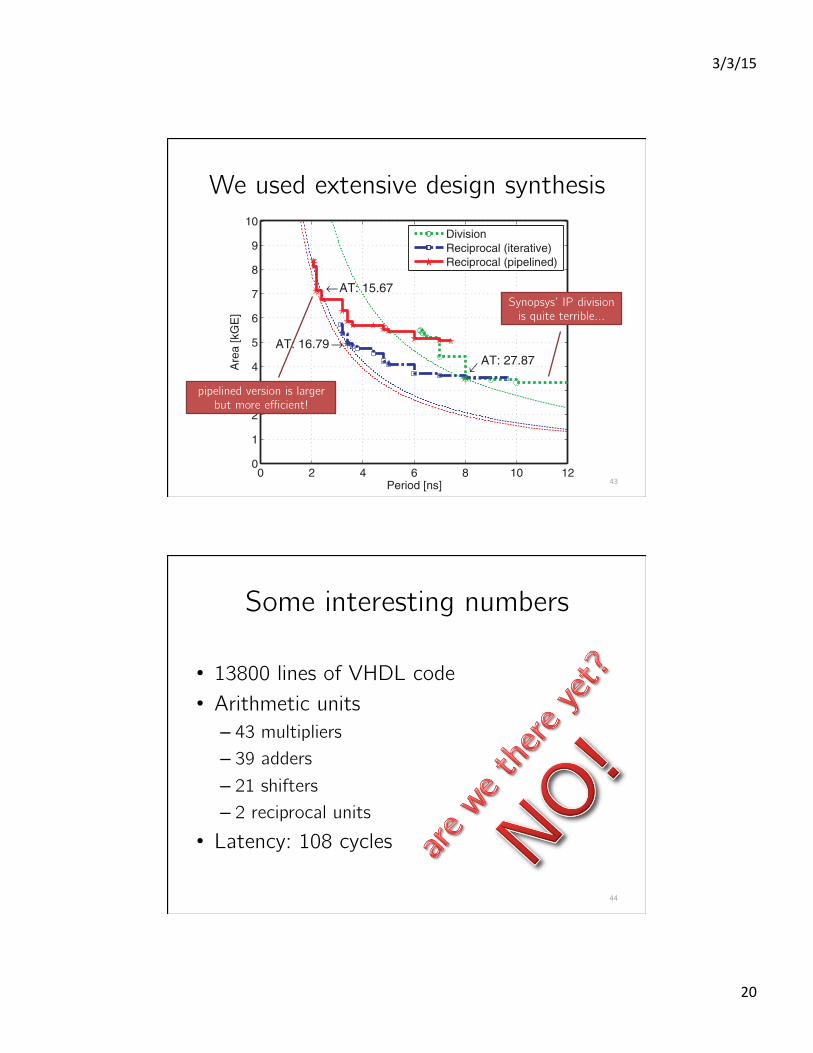
Some interesting numbers!
• 13800 lines of VHDL code!• Arithmetic units!– 43 multipliers!– 39 adders!– 21 shifters!– 2 reciprocal units!
• Latency: 108 cycles!
44!

3/3/15
21
Design for test and measurement!Step 6!
45!
Testing is important!
• Testing is among the most expensive (and tedious) aspects of digital VLSI design:!– Testing easily requires >50% of the design effort!– Debug time after fabrication incurs enormous costs!
• Example: Intel FDIV bug (1994)!– Logic error found after >1M parts shipped!– Recall cost $450M; image loss is much worse!
• Main goal: First time right!!46!

3/3/15
22
47!
“If you don’t test it,! it won’t work (guaranteed)”!
- unknown!
Observability and controllability!
• Observability: able to observe internal node by watching external output (=pins) of chip!
• Controllability: able to force internal node to 0 and 1 via inputs (=pins) of the chip!
• Combinational logic: nodes are rather easy to control and observe!
• Sequential logic: extremely difficult or even impossible to control and observe!
48!

3/3/15
23
Design for test (DFT)!• Idea: Design the chip to increase
observability and controllability!
• If each register could be observed and controlled, testing reduces to testing combinational logic between registers!
• Even better: logic could enter test mode where they test themselves automatically!
49!
add test structures already
during design!
Use scan chains!!• Convert each flip-flop to a scan register!– Cost = one MUX!– Scan mode: FFs behave !
as a long shift register!
50!
Flop QD
CLK
SISCAN
scan out
scan-in
inputs outputs
Flop
Flop
Flop
Flop
Flop
Flop
Flop
Flop
Flop
Flop
Flop
Flop
LogicCloud
LogicCloud
in scan mode, we can set
and read the state of each
flip-flop!

3/3/15
24
compile_ultra –scan
# -------------------------------------------------------------------# Insert DFT# -------------------------------------------------------------------
reset_dft_configuration
# -- define partial scan chainsset_scan_group ram_chain -access [ list ScanDataIn InputMemory/ScanInxTI \ ScanDataOut InputMemory/ScanOutxTO \ ScanEnable InputMemory/ScanEnxTI ] \ -serial_routed true -include_elements InputMemory
set_scan_configuration -replace falseset_scan_configuration -style multiplexed_flip_flopset_scan_configuration -clock_mixing no_mix
set_dft_signal -view spec -type ScanClock -port ClkxCIset_dft_signal -view spec -type ScanEnable -port ScanEnxTI -active_state 1
Synopsys DC can help you!
51!
# -- create 8 chainsset_scan_configuration -chain_count 8
set_dft_signal -view spec -type ScanDataIn -port DataxDI[0]set_dft_signal -view spec -type ScanDataIn -port DataxDI[1]set_dft_signal -view spec -type ScanDataIn -port DataxDI[2]set_dft_signal -view spec -type ScanDataIn -port DataxDI[3]set_dft_signal -view spec -type ScanDataIn -port DataxDI[4]set_dft_signal -view spec -type ScanDataIn -port DataxDI[5]set_dft_signal -view spec -type ScanDataIn -port DataxDI[6]set_dft_signal -view spec -type ScanDataIn -port DataxDI[7]
set_dft_signal -view spec -type ScanDataOut -port LLRxDO[0]set_dft_signal -view spec -type ScanDataOut -port LLRxDO[1]set_dft_signal -view spec -type ScanDataOut -port LLRxDO[2]set_dft_signal -view spec -type ScanDataOut -port LLRxDO[3]set_dft_signal -view spec -type ScanDataOut -port LLRxDO[4]set_dft_signal -view spec -type ScanDataOut -port LLRxDO[5]set_dft_signal -view spec -type ScanDataOut -port LLRxDO[6]set_dft_signal -view spec -type ScanDataOut -port LLRxDO[7]
create_test_protocol -infer_async -infer_clockset_dft_insertion_configuration -synthesis_optimization none
dft_drc > reports/scanchain.rep
# -- insert scan chainsinsert_dft
preview_dft -show cells >> reports/scanchain.rep !example scripts !for a different design!!
DFT specs!
• We used a full-scan strategy: All flip-flops are included in scan chains!
• We used multiple parallel scan chains à lowers load and readout time!
• Test patterns were generated automatically with Synopsys Tetramax à ATPG!
• We achieved over 98% test coverage!– Commercial chips require far higher coverage!
52!

3/3/15
25
Power measurements!
• Our goal was to measure the dynamic power consumption of each PE!
• We did not have enough IO to use 8 independent VDD and GND pins!
• What can we do?!
53!
Simple solution: Clock gating!
• We can turn of the clock within each PE (starting from 1 to 7)!
54!

3/3/15
26
Max. throughput measurements!• Used package will !
require relatively long !bonding wires !
• We had no PLL L !• Max. clock frequency !
we can get into the !ASIC with our test equipment is ~400MHz!
• What can we do?!55!
XOR trick!• Create 2 clocks with 90° phase shift and
multiply them with an on-chip XOR gate!!
• This approach has a fallback mode: Just set CLK2=0 and you will only see CLK1 internally!!
56!
CLK1!
CLK2! twice the external!frequency!!
internal clock signal!

3/3/15
27
Multiple synthesis runs for final design!
57!
we varied the timing constraint!
we decided to pick the design with best HE!
Backend design!Step 7!
58!

3/3/15
28
Backend design!
• We used Cadence SoC Encounter !• We placed & routed our design at least 20x!– With different timing or placement constraints!– With different Synopsys constraints!
• We manually retimed some pipeline registers in VHDL to increase the clock frequency!
• One back-end run required about 6 hours!!59!use scripts!!
Carefully design your IO interface!
60!
only 56 pins!
QFN56 package!
scan chain inputs and
outputs shared !

3/3/15
29
Final floorplan!
61!
only 56 pins!
always use a power
grid!
artwork on top metal
layer! cell density is 86%!
no SRAMs!
Post-layout verification/timing!• According to post-layout timing extraction,
the design should achieve 622MHz!• We performed an excessive number of post-
layout design verifications and tests!– Annotated Modelsim simulations with stimuli
and expected responses from golden model!– Extracted power estimates!
• We also performed DRC and LVS in Cadence prior to tape-out (never forget!)!
62!
one simulation run took about
5 hours!

3/3/15
30
Tapeout!!• UMC = United Microelectronics Corp.!• Taiwan-based silicon foundry!!• ASIC got fabricated on a so-called multi-
project wafer !
• Fabrication took !about 4-5 months!
63!
This is what we got back!
64!
chip micrograph! packaged ASIC!

3/3/15
31
Initial tests!Step 8!
65!
This photo shows a similar tester we had at ETH!
Do the chips work?!• We used an HP83000 production tester!
66!
power supply!
& cooling!
test channels!= array of high-end
oscilloscopes & pattern generators!
device under test (DUT) PCB!
ASIC!
old Solaris workstation!

3/3/15
32
The DUT board!
67!
Prepare stimuli/expected responses!
68!
INPClkxCI,Clk2xCI,ResetxRBI,ResetConfigxRBI,EvenParityxDI,OddParityxDI,SystematicxDI,ModexSI,LoopxSI,ScanEnxTI,TestModexTI,BistEnxTI;
OUTStatus,LLREven,LLROdd,BistDone,BistOk;
PERIOD6ns;
TIME_UNIT1ns;
TABLE_FORMATD c c c c ccccc ccccc ccccc ccc c c c c ccc cccccc cccccc c c;
DATA_SECTION90 1 0 0 0 00000 00000 00000 000 0 0 0 0 --- ------ ------ - -190 1 0 1 1 00000 00000 00000 011 0 0 0 0 --- ------ ------ - -290 1 0 1 1 00000 00000 00000 011 0 0 0 0 --- ------ ------ - -390 1 0 1 1 00010 00000 01110 011 0 0 0 0 --- ------ ------ - -490 1 0 1 1 00010 00000 01110 011 0 0 0 0 --- ------ ------ - -590 1 0 1 1 00000 00000 00000 011 0 0 0 0 --- ------ ------ - -690 1 0 1 1 00000 00000 00000 011 0 0 0 0 --- ------ ------ - -790 1 0 1 1 00000 00001 01110 011 0 0 0 0 --- ------ ------ - -890 1 0 1 1 00010 00000 01110 011 0 0 0 0 --- ------ ------ - -990 1 0 1 1 01101 00000 10111 011 0 0 0 0 --- ------ ------ - -1090 1 0 1 1 00011 00000 10111 011 0 0 0 0 --- ------ ------ - -1190 1 0 1 1 10100 00000 00000 011 0 0 0 0 --- ------ ------ - -1290 1 0 1 1 00000 00000 00000 011 0 0 0 0 --- ------ ------ - -1390 1 0 1 1 01000 00001 00000 011 0 0 0 0 --- ------ ------ - -1490 1 0 1 1 00000 00000 00111 011 0 0 0 0 --- ------ ------ - -1590 1 0 1 1 00000 00000 00000 000 0 0 0 0 --- ------ ------ - -1690 1 0 0 1 00000 00000 00000 100 0 0 0 0 --- ------ ------ - -1790 1 0 1 1 01111 01000 01001 100 0 0 0 0 --- ------ ------ - -1890 1 0 1 1 01111 01000 01001 100 0 0 0 0 --- ------ ------ - -1990 1 0 1 1 11101 11010 00101 100 0 0 0 0 --- ------ ------ - -2090 1 0 1 1 11101 11010 00101 100 0 0 0 0 --- ------ ------ - -2190 1 0 1 1 11100 01100 00101 100 0 0 0 0 --- ------ ------ - -2290 1 0 1 1 11100 01100 00101 100 0 0 0 0 --- ------ ------ - -2390 1 0 1 1 01111 11100 10111 100 0 0 0 0 --- ------ ------ - -2490 1 0 1 1 01111 11100 10111 100 0 0 0 0 --- ------ ------ - -2590 1 0 1 1 00100 11010 01110 100 0 0 0 0 --- ------ ------ - -2690 1 0 1 1 00100 11010 01110 100 0 0 0 0 --- ------ ------ - -2790 1 0 1 1 11111 10101 11101 100 0 0 0 0 --- ------ ------ - -2890 1 0 1 1 11111 10101 11101 100 0 0 0 0 011 000000 000000 - -2990 1 0 1 1 00010 00011 10001 100 0 0 0 0 011 000000 000000 - -3090 1 0 1 1 00010 00011 10001 100 0 0 0 0 011 000000 000000 - -!
stimuli and responses !for a different design!!

3/3/15
33
Milestone 1: get a life sign!
• First just reset the chip and measure power supplies (current etc.; prevents shorts)!
• Use the simplest functional test you can think of to see whether you chip is working!– We used a simple data read-in read-out test!
• You need a detailed datasheet of the design (believe me, you forgot how it worked)!
69!
A safe timing scheme for first tests!
70!
clock period!
• What clock period should I use?!• When to apply stimuli?!• When to sample responses?!

3/3/15
34
A safe timing scheme for first tests!
71!
clock period = 100ns!
stimuli!application!
10ns!
response!sampling!90ns!
plenty of time to
meet setup time!
plenty of time to exceed
propagation delay!
plenty of time to not violate hold
times!
The MMSE PIC ASIC works!!!!
72!This is real photo of the screen when it first worked!!

3/3/15
35
Performance measurements!Step 9!
73!
What do we want to measure?!
• Maximum clock frequency!• Power consumption!– For random stimuli!– For real-world stimuli!– For individual PEs!
• Input delay (setup)!• Output delay (propagation)!• Hold time!
74!

3/3/15
36
How to measure timing?!
75!
stimuli!application!
response!sampling!
hold time!
Repeat tests until ASIC fails!!
Input delay (setup time)!
76!
stimuli!application!
response!sampling!
input delay!
Repeat tests until ASIC fails!!

3/3/15
37
Output delay (prop. delay)!
77!
stimuli!application!
response!sampling!
propagation delay!
Repeat tests until ASIC fails!!
Max. clock frequency!
78!
stimuli!application!
response!sampling!
max. clock frequency!
Repeat tests until ASIC fails!!

3/3/15
38
Voltage-frequency scaling!
• Vary clock period versus supply voltage!
• Generate so-called Shmoo plot !
• Red = fail!• Green = pass!
79!Schmoo plot of another design!
Power measurements!
• We ran the ASIC at full speed and measured the current on the DUT board!– Simply use P = V*I!– Use meaningful stimuli (realistic data!)!– Note the temperature!!
• We used our clock-gating scheme to measure power in individual PEs!
80!

3/3/15
39
Performance summary!
What Simulated Measured
Max. clock frequency 622 MHz 568 MHz
Max. throughput 829 MB/s 757 Mb/s
Power consumpXon ? 769 mWa or 189.1 mWb
Energy efficiency ? 1.02 nJ/bita or 0.25 nJ/bitb
81!
a measured with random stimuli!b measured with real-world stimuli!
• All power measurements for Vdd=1.2V core supply and at T=300K!
• All 10 out of 10 packaged ASICs were fully functional!
example of a bad datasheet L !
always specify this!!
Publish & advertise!Step 10!
82!

3/3/15
40
Two publications in 2010/2011 !• ESSCIRC (failed at VLSI symp.)!
• JSSC (invited paper)!
83!
Swisscom innovation award 2010!
• We won CHF 10k!
84!

3/3/15
41
Take-home messages!• Use domain-specific knowledge!• Algorithm optimizations usually help much
more than circuit optimizations!• Write a detailed datasheet (you will need it)!• Think about testing/measuring while you
design your chip à DFT!• You cannot verify/test your design enough!• Did I mention you have to verify your design?!• Publications: Either be the first or the best!
86!
Questions?!
87!