Embed Size (px)
Citation preview
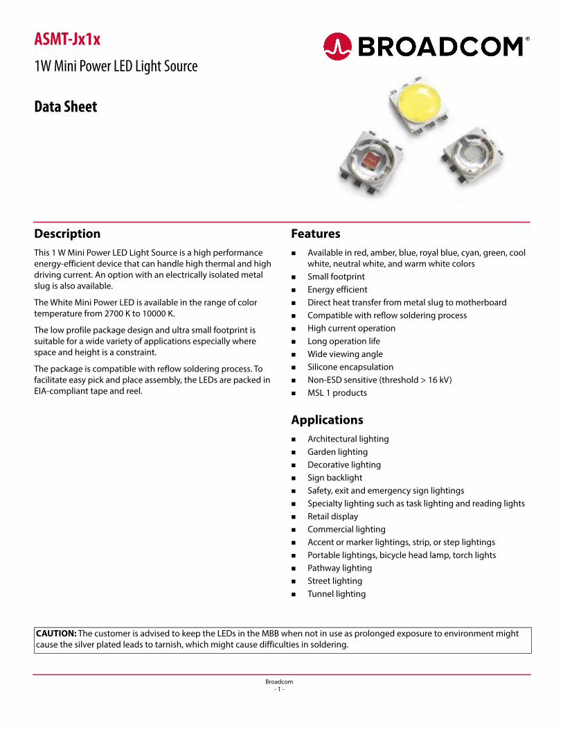
ASMT-Jx1x1W Mini Power LED Light Source
Data Sheet
DescriptionThis 1 W Mini Power LED Light Source is a high performance energy-efficient device that can handle high thermal and high driving current. An option with an electrically isolated metal slug is also available.
The White Mini Power LED is available in the range of color temperature from 2700 K to 10000 K.
The low profile package design and ultra small footprint is suitable for a wide variety of applications especially where space and height is a constraint.
The package is compatible with reflow soldering process. To facilitate easy pick and place assembly, the LEDs are packed in EIA-compliant tape and reel.
Features Available in red, amber, blue, royal blue, cyan, green, cool
white, neutral white, and warm white colors Small footprint Energy efficient Direct heat transfer from metal slug to motherboard Compatible with reflow soldering process High current operation Long operation life Wide viewing angle Silicone encapsulation Non-ESD sensitive (threshold > 16 kV) MSL 1 products
Applications Architectural lighting Garden lighting Decorative lighting Sign backlight Safety, exit and emergency sign lightings Specialty lighting such as task lighting and reading lights Retail display Commercial lighting Accent or marker lightings, strip, or step lightings Portable lightings, bicycle head lamp, torch lights Pathway lighting Street lighting Tunnel lighting
CAUTION: The customer is advised to keep the LEDs in the MBB when not in use as prolonged exposure to environment might cause the silver plated leads to tarnish, which might cause difficulties in soldering.
Broadcom- 1 -
ASMT-Jx1x Data Sheet
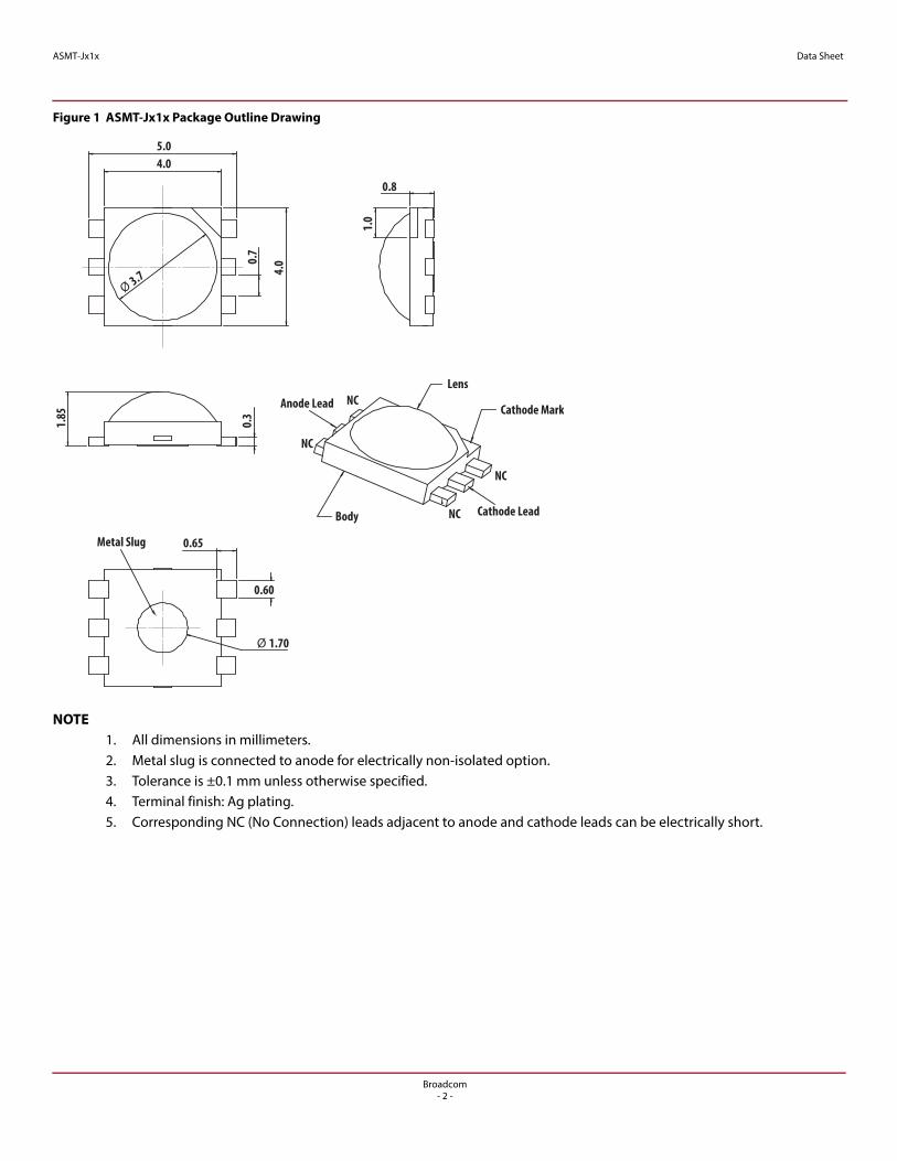
Figure 1 ASMT-Jx1x Package Outline Drawing
NOTE1. All dimensions in millimeters.2. Metal slug is connected to anode for electrically non-isolated option.3. Tolerance is ±0.1 mm unless otherwise specified.4. Terminal finish: Ag plating.5. Corresponding NC (No Connection) leads adjacent to anode and cathode leads can be electrically short.
5.04.0
4.00.
7
1.0
0.3
1.85
Ø 3.7
0.8
0.65
0.60
Ø 1.70
Body Cathode Lead
Lens
Cathode MarkAnode Lead NC
NC
NC
NC
Metal Slug
Broadcom- 2 -

ASMT-Jx1x Data Sheet
Device Selection Guide (TJ = 25°C)
Absolute Maximum Ratings
Part Number Color
Luminous Flux (lm) / Radiometric Power (mW), V a, b
a. V is the total luminous flux/radiometric power output as measured with an integrating sphere at 25-ms mono pulse condition.
b. Flux tolerance is ±10 %.
Test Current (mA)
Dice Technology
Electrically Isolated
Metal SlugMin. Typ. Max.
ASMT-JR10-AST01 Red 51.7 62.0 87.4 350 AllnGaP No
ASMT-JA10-ARS01 Amber 39.8 48.0 67.2 350 AllnGaP No
ASMT-JB11-NNQ01 Blue 18.1 24.0 39.8 350 InGaN Yes
ASMT-JL11-NQS01 Royal Blue 435 mW 550 mW 685 mW 350 InGaN Yes
ASMT-JC11-NTU01 Cyan 67.2 75.0 99.6 350 InGaN Yes
ASMT-JG11-NUW01 Green 87.4 110.0 129.5 350 InGaN Yes
ASMT-JW11-NWX01 Cool White 113.6 120.0 147.7 350 InGaN Yes
ASMT-JN11-NWX01 Neutral White 113.6 120.0 147.7 350 InGaN Yes
ASMT-JY11-NVW01 Warm White 99.6 105.0 129.5 350 InGaN Yes
Parameter AllnGaP InGaN InGaN Cyan Units
DC Forward Currenta
a. Derate linearly based on Figure 13 and Figure 14 for AlInGaP and Figure 25 and Figure 26 for InGaN.
500 500 500 mA
Peak Pulsing Currentb
b. Pulse condition duty factor = 10%, Frequency = 1 kHz.
1000 1000 1000 mA
Power Dissipation 1230 1830 1980 mW
LED Junction Temperature 125 150 150 °C
Operating Metal Slug Temperature Range at 350 mA –40 to +115 –40 to +135 –40 to +135 °C
Storage Temperature Range –40 to +120 –40 to +120 –40 to +120 °C
Soldering Temperature See Figure 29
Reverse Voltagec
c. Not recommended for reverse bias operation.
Not recommended
Broadcom- 3 -
ASMT-Jx1x Data Sheet
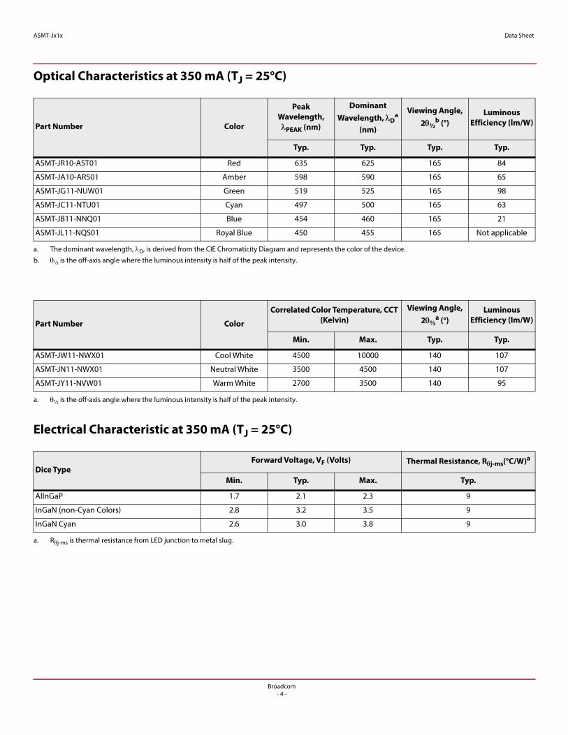
Optical Characteristics at 350 mA (TJ = 25°C)
Electrical Characteristic at 350 mA (TJ = 25°C)
Part Number Color
Peak Wavelength, PEAK (nm)
Dominant Wavelength, D
a (nm)
a. The dominant wavelength, D, is derived from the CIE Chromaticity Diagram and represents the color of the device.
Viewing Angle, 2½
b (°)
b. ½ is the off-axis angle where the luminous intensity is half of the peak intensity.
Luminous Efficiency (lm/W)
Typ. Typ. Typ. Typ.
ASMT-JR10-AST01 Red 635 625 165 84
ASMT-JA10-ARS01 Amber 598 590 165 65
ASMT-JG11-NUW01 Green 519 525 165 98
ASMT-JC11-NTU01 Cyan 497 500 165 63
ASMT-JB11-NNQ01 Blue 454 460 165 21
ASMT-JL11-NQS01 Royal Blue 450 455 165 Not applicable
Part Number Color
Correlated Color Temperature, CCT (Kelvin)
Viewing Angle, 2½
a (°)
a. ½ is the off-axis angle where the luminous intensity is half of the peak intensity.
Luminous Efficiency (lm/W)
Min. Max. Typ. Typ.
ASMT-JW11-NWX01 Cool White 4500 10000 140 107
ASMT-JN11-NWX01 Neutral White 3500 4500 140 107
ASMT-JY11-NVW01 Warm White 2700 3500 140 95
Dice TypeForward Voltage, VF (Volts) Thermal Resistance, Rj-ms(°C/W)a
a. Rj-ms is thermal resistance from LED junction to metal slug.
Min. Typ. Max. Typ.
AllnGaP 1.7 2.1 2.3 9
InGaN (non-Cyan Colors) 2.8 3.2 3.5 9
InGaN Cyan 2.6 3.0 3.8 9
Broadcom- 4 -
ASMT-Jx1x Data Sheet
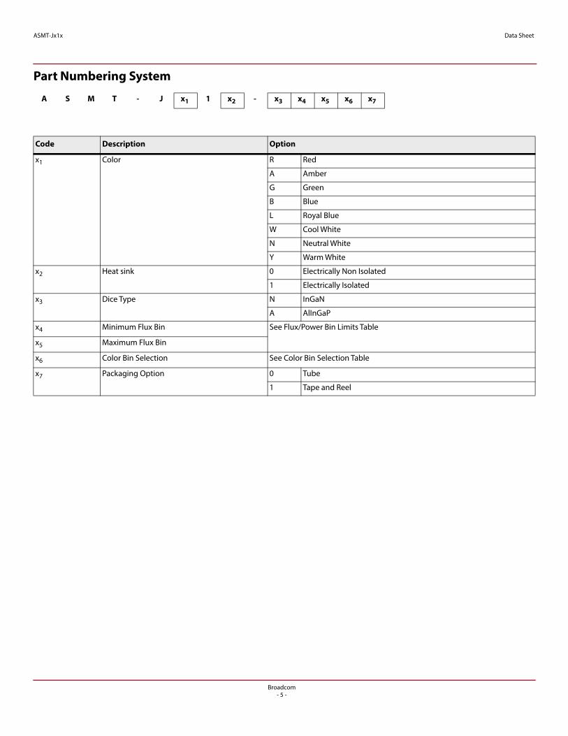
Part Numbering System
A S M T - J x1 1 x2 - x3 x4 x5 x6 x7
Code Description Option
x1 Color R Red
A Amber
G Green
B Blue
L Royal Blue
W Cool White
N Neutral White
Y Warm White
x2 Heat sink 0 Electrically Non Isolated
1 Electrically Isolated
x3 Dice Type N InGaN
A AlInGaP
x4 Minimum Flux Bin See Flux/Power Bin Limits Table
x5 Maximum Flux Bin
x6 Color Bin Selection See Color Bin Selection Table
x7 Packaging Option 0 Tube
1 Tape and Reel
Broadcom- 5 -
ASMT-Jx1x Data Sheet
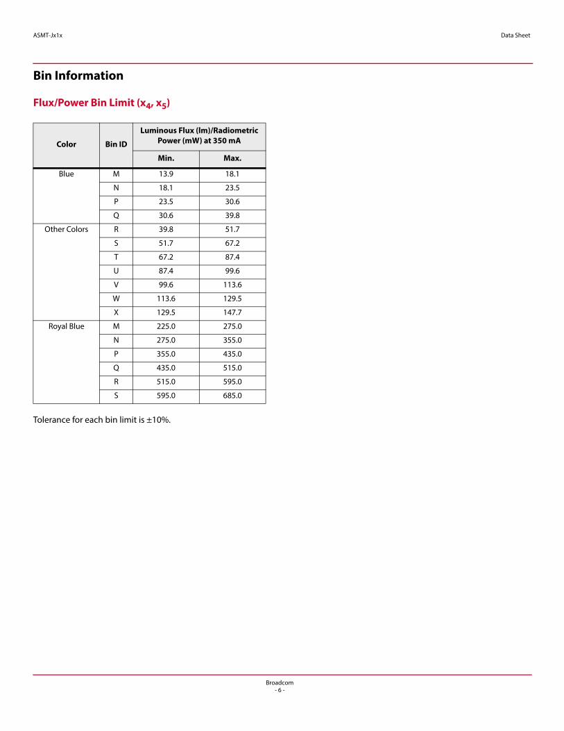
Bin Information
Flux/Power Bin Limit (x4, x5)
Tolerance for each bin limit is ±10%.
Color Bin ID
Luminous Flux (lm)/Radiometric Power (mW) at 350 mA
Min. Max.
Blue M 13.9 18.1
N 18.1 23.5
P 23.5 30.6
Q 30.6 39.8
Other Colors R 39.8 51.7
S 51.7 67.2
T 67.2 87.4
U 87.4 99.6
V 99.6 113.6
W 113.6 129.5
X 129.5 147.7
Royal Blue M 225.0 275.0
N 275.0 355.0
P 355.0 435.0
Q 435.0 515.0
R 515.0 595.0
S 595.0 685.0
Broadcom- 6 -

ASMT-Jx1x Data Sheet
Color Bin Selection (x6)
Individual reel will contain parts from one color bin selection only.
Cool White
Warm White
Neutral White
Other Colors
Selection Bin ID
0 Full Distribution
E VM, UM, VN, and UN
F WM, VM, WN, and VN
G XM, WM, XN, and WN
H UN, VN, U0, and V0
J WN, VN, W0, and V0
K XN, WN, X0, and W0
L V0, U0, VP, and UP
M W0, V0, WP, VP, and WQ
N X0, W0, XP, WP, and WQ
P Y0
Q YA
Selection Bin ID
0 Full Distribution
E NM, MM, N1, and M1
F PM, NM, P1, and N1
G QM, PM, Q1, and P1
H M1, N1, M0, and N0
J P1, N1, P0, and N0
K Q1, P1, Q0, and P0
L N0, M0, NA, and MA
M P0, N0, PA, and NA
N Q0, P0, QA, and PA
Selection Bin ID
0 Full Distribution
E SM, RM, S1, and R1
F TM, SM, TN, and S1
G S1, R1, S0, and R0
H TN, S1, T0, and S0
J S0, R0, SA, and RA
K T0, S0, TP, and SA
Selection Bin ID
0 Full Distribution
Z A and B
Y B and C
W C and D
V D and E
Q A, B, and C
P B, C, and D
N C, D, and E
M D, E, and F
Broadcom- 7 -

ASMT-Jx1x Data Sheet
Figure 2 Color Bin Structure for Cool White Figure 3 Color Bin Structure for Warm White
0.26
0.28
0.30
0.32
0.34
0.36
0.38
0.40
0.42
0.26 0.28 0.30 0.32 0.34 0.36 0.38 0.40X-COORDINATE
Y-CO
ORDI
NATE
10000K
7000K
6300K
5000K4500K
Y0
YA
UM
UN
UPV0
VMVN
VPX0
XP
XM
XN W0
WQ
U0WMWN
WP
5650K
BLACK BODY CURVE
0.32
0.34
0.36
0.38
0.40
0.42
0.44
0.46
0.48
0.38 0.40 0.42 0.44 0.46 0.48 0.50X-COORDINATE
Y-CO
ORDI
NATE QM
MMNM
Q1
QA
P1M0
M1
MANA
3050K 2850K3500K
3250K2700K
PM
Q0 P0
PABLACK BODY CURVE
N1
N0
Figure 4 Color Bin Structure for Neutral White
0.32
0.34
0.36
0.38
0.40
0.42
0.44
0.46
0.34 0.36 0.38 0.40 0.42 0.44X-COORDINATE
Y-CO
ORDI
NATE
RM
R1
R0
RAT0
SM
S1
SA
TM
TN
TP
S0
4500K
BLACK BODY CURVE
4100K3800K
3500K
Broadcom- 8 -
ASMT-Jx1x Data Sheet
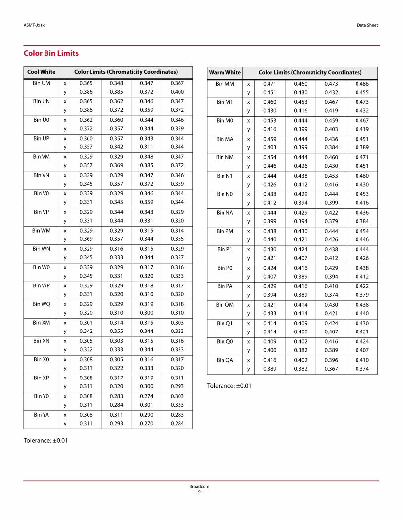
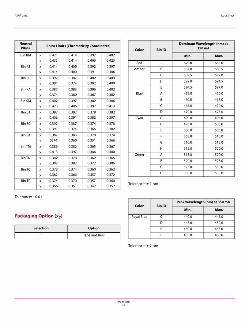
Color Bin Limits
Tolerance: ±0.01
Tolerance: ±0.01
Cool White Color Limits (Chromaticity Coordinates)
Bin UM xy
0.3650.386
0.3480.385
0.3470.372
0.3670.400
Bin UN xy
0.3650.386
0.3620.372
0.3460.359
0.3470.372
Bin U0 xy
0.3620.372
0.3600.357
0.3440.344
0.3460.359
Bin UP xy
0.3600.357
0.3570.342
0.3430.311
0.3440.344
Bin VM xy
0.3290.357
0.3290.369
0.3480.385
0.3470.372
Bin VN xy
0.3290.345
0.3290.357
0.3470.372
0.3460.359
Bin V0 xy
0.3290.331
0.3290.345
0.3460.359
0.3440.344
Bin VP xy
0.3290.331
0.3440.344
0.3430.331
0.3290.320
Bin WM xy
0.3290.369
0.3290.357
0.3150.344
0.3140.355
Bin WN xy
0.3290.345
0.3160.333
0.3150.344
0.3290.357
Bin W0 xy
0.3290.345
0.3290.331
0.3170.320
0.3160.333
Bin WP xy
0.3290.331
0.3290.320
0.3180.310
0.3170.320
Bin WQ xy
0.3290.320
0.3290.310
0.3190.300
0.3180.310
Bin XM xy
0.3010.342
0.3140.355
0.3150.344
0.3030.333
Bin XN xy
0.3050.322
0.3030.333
0.3150.344
0.3160.333
Bin X0 xy
0.3080.311
0.3050.322
0.3160.333
0.3170.320
Bin XP xy
0.3080.311
0.3170.320
0.3190.300
0.3110.293
Bin Y0 xy
0.3080.311
0.2830.284
0.2740.301
0.3030.333
Bin YA xy
0.3080.311
0.3110.293
0.2900.270
0.2830.284
Warm White Color Limits (Chromaticity Coordinates)
Bin MM xy
0.4710.451
0.4600.430
0.4730.432
0.4860.455
Bin M1 xy
0.4600.430
0.4530.416
0.4670.419
0.4730.432
Bin M0 xy
0.4530.416
0.4440.399
0.4590.403
0.4670.419
Bin MA xy
0.4590.403
0.4440.399
0.4360.384
0.4510.389
Bin NM xy
0.4540.446
0.4440.426
0.4600.430
0.4710.451
Bin N1 xy
0.4440.426
0.4380.412
0.4530.416
0.4600.430
Bin N0 xy
0.4380.412
0.4290.394
0.4440.399
0.4530.416
Bin NA xy
0.4440.399
0.4290.394
0.4220.379
0.4360.384
Bin PM xy
0.4380.440
0.4300.421
0.4440.426
0.4540.446
Bin P1 xy
0.4300.421
0.4240.407
0.4380.412
0.4440.426
Bin P0 xy
0.4240.407
0.4160.389
0.4290.394
0.4380.412
Bin PA xy
0.4290.394
0.4160.389
0.4100.374
0.4220.379
Bin QM xy
0.4210.433
0.4140.414
0.4300.421
0.4380.440
Bin Q1 xy
0.4140.414
0.4090.400
0.4240.407
0.4300.421
Bin Q0 xy
0.4090.400
0.4020.382
0.4160.389
0.4240.407
Bin QA xy
0.4160.389
0.4020.382
0.3960.367
0.4100.374
Broadcom- 9 -
ASMT-Jx1x Data Sheet
Tolerance: ±0.01
Packaging Option (x7)
Tolerance: ± 1 nm
Tolerance: ± 2 nm
Neutral White Color Limits (Chromaticity Coordinates)
Bin RM xy
0.4210.433
0.4140.414
0.3970.406
0.4020.423
Bin R1 xy
0.4140.414
0.4090.400
0.3920.391
0.3970.406
Bin R0 xy
0.3920.391
0.3870.374
0.4020.382
0.4090.400
Bin RA xy
0.3870.374
0.3830.360
0.3960.367
0.4020.382
Bin SM xy
0.4020.423
0.3970.406
0.3820.397
0.3860.413
Bin S1 xy
0.3970.406
0.3920.391
0.3780.382
0.3820.397
Bin S0 xy
0.3920.391
0.3870.374
0.3740.366
0.3780.382
Bin SA xy
0.3870374
0.3830.360
0.3700.351
0.3740.366
Bin TM xy
0.3860.413
0.3820.397
0.3650.386
0.3670.400
Bin TN xy
0.3820.397
0.3780.382
0.3620.372
0.3650.386
Bin T0 xy
0.3780.382
0.3740.366
0.3600.357
0.3620.372
Bin TP xy
0.3740.366
0.3700.351
0.3570.342
0.3600.357
Selection Option
1 Tape and Reel
Color Bin ID
Dominant Wavelength (nm) at 350 mA
Min. Max.
Red — 620.0 635.0
Amber B 587.0 589.5
C 589.5 592.0
D 592.0 594.5
E 594.5 597.0
Blue A 455.0 460.0
B 460.0 465.0
C 465.0 470.0
D 470.0 475.0
Cyan C 490.0 495.0
D 495.0 500.0
E 500.0 505.0
F 505.0 510.0
G 510.0 515.0
H 515.0 520.0
Green A 515.0 520.0
B 520.0 525.0
C 525.0 530.0
D 530.0 535.0
Color Bin IDPeak Wavelength (nm) at 350 mA
Min. Max.
Royal Blue C 440.0 445.0
D 445.0 450.0
E 450.0 455.0
F 455.0 460.0
Broadcom- 10 -
ASMT-Jx1x Data Sheet
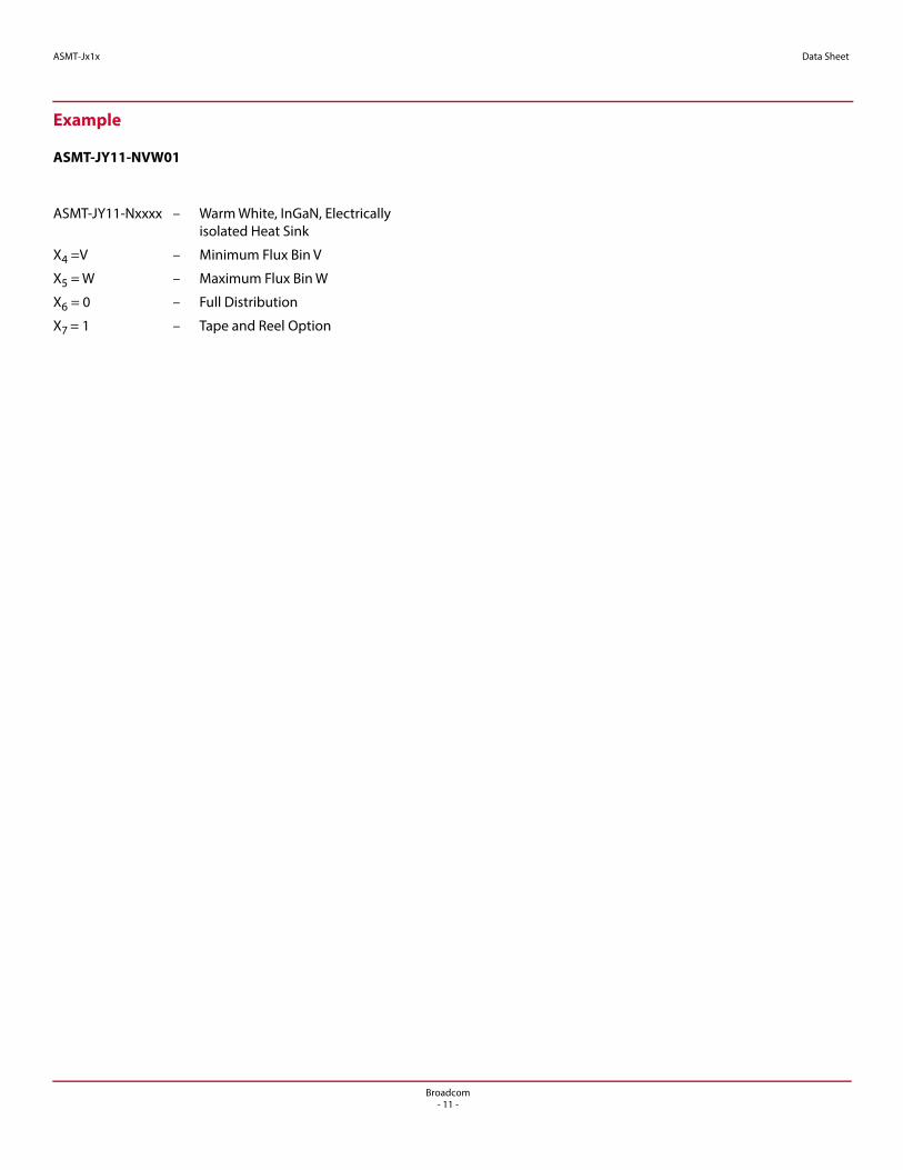
Example
ASMT-JY11-NVW01
ASMT-JY11-Nxxxx – Warm White, InGaN, Electrically isolated Heat Sink
X4 =V – Minimum Flux Bin V
X5 = W – Maximum Flux Bin W
X6 = 0 – Full Distribution
X7 = 1 – Tape and Reel Option
Broadcom- 11 -
ASMT-Jx1x Data Sheet
AlInGaP
Figure 5 Relative Intensity vs. Wavelength for Red and Amber Figure 6 Relative Luminous Flux vs. Mono Pulse Current
00.10.20.30.40.50.60.70.80.9
1
530 545 560 575 590 605 620 635 650 665 680WAVELENGTH - nm
RELA
TIVE
INTE
NSIT
Y
AMBER
RED
0
0.2
0.4
0.6
0.8
1
1.2
1.4
1.6
0 100 200 300 400 500DC FORWARD CURRENT - mA
RELA
TIVE
LUM
INOU
S FLU
X(N
ORM
ALIZ
ED A
T 350
mA)
Figure 7 Forward Current vs. Forward Voltage Figure 8 Radiation Pattern for Red and Amber
050
100150200250300350400450500
0 0.5 1 1.5 2 2.5 3FORWARD VOLTAGE - V
FORW
ARD
CURR
ENT -
mA
00.10.20.30.40.50.60.70.80.9
1
-90 -60 -30 0 30 60 90ANGULAR DISPLACEMENT - DEGREES
NORM
ALIZ
ED IN
TENS
ITY
Figure 9 Maximum Pulse Current vs. Ambient Temperature. Derated based on TA = 25°C, RJ-A = 50°C/W.
Figure 10 Maximum Pulse Current vs. Ambient Temperature. Derated based on TA = 85°C, RJ-A = 50°C/W.
0.0
0.2
0.4
0.6
0.8
1.0
1.2
1.4
0.00001 0.0001 0.001 0.01 0.1 1 10 100
PULSE DURATION, tp - sec
PULS
E CUR
RENT
, IP -
A
D =0.050.100.250.501.00
0.0
0.2
0.4
0.6
0.8
1.0
1.2
1.4
0.00001 0.0001 0.001 0.01 0.1 1 10 100
PULSE DURATION, tp - sec
PULS
E CUR
RENT
, IP -
A
D =0.050.100.250.501.00
Broadcom- 12 -
ASMT-Jx1x Data Sheet
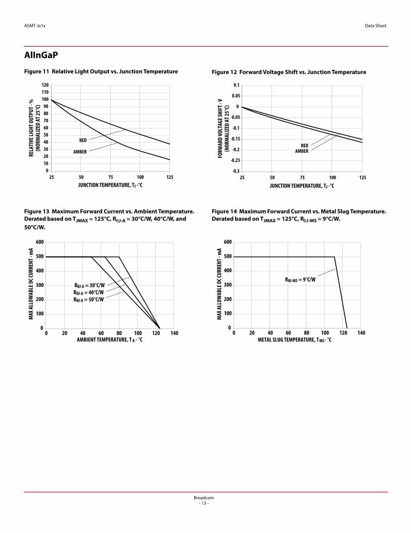
AlInGaP
Figure 11 Relative Light Output vs. Junction Temperature Figure 12 Forward Voltage Shift vs. Junction Temperature
0102030405060708090
100110120
25 50 75 100 125
RELA
TIVE
LIGH
T OUT
PUT -
%(N
ORM
ALIZ
ED A
T 25°
C)
JUNCTION TEMPERATURE, TJ -°C
RED
AMBER
-0.3
-0.25
-0.2
-0.15
-0.1
-0.05
0
0.05
0.1
25 50 75 100 125
FORW
ARD
VOLT
AGE S
HIFT
- V(N
ORM
ALIZ
ED A
T 25°
C)
JUNCTION TEMPERATURE, TJ -°C
REDAMBER
Figure 13 Maximum Forward Current vs. Ambient Temperature. Derated based on TJMAX = 125°C, RJ-A = 30°C/W, 40°C/W, and 50°C/W.
Figure 14 Maximum Forward Current vs. Metal Slug Temperature. Derated based on TJMAX = 125°C, RJ-MS = 9°C/W.
0
100
200
300
400
500
600
0 20 40 60 80 100 120 140AMBIENT TEMPERATURE, T A - °C
MAX
ALL
OWAB
LE D
C CUR
RENT
- mA
RθJ-A = 30°C/WRθJ-A = 40°C/WRθJ-A = 50°C/W
0
100
200
300
400
500
600
0 20 40 60 80 100 120 140METAL SLUG TEMPERATURE, T MS - °C
MAX
ALL
OWAB
LE D
C CUR
RENT
- mA
RθJ-MS = 9°C/W
Broadcom- 13 -

ASMT-Jx1x Data Sheet
InGaN
Figure 15 Relative Intensity vs. Wavelength for Cool, Neutral, and Warm White
Figure 16 Relative Intensity vs. Wavelength for Blue, Royal Blue, Cyan, and Green
00.10.20.30.40.50.60.70.80.9
1
380 480 580 680 780
RELA
TIVE
INTE
NSIT
Y
WAVELENGTH - nm
WARM WHITE
NEUTRAL WHITE
COOL WHITE
00.10.20.30.40.50.60.70.80.9
1
380 405 430 455 480 505 530 555 580 605 630WAVELENGTH - nm
RELA
TIVE
INTE
NSIT
Y
GREEN
BLUEROYAL BLUE
CYAN
Figure 17 Relative Luminous Flux vs. Mono Pulse Current Figure 18 Forward Current vs. Forward Voltage
0
0.2
0.4
0.6
0.8
1
1.2
1.4
0 100 200 300 400 500DC FORWARD CURRENT - mA
RELA
TIVE
LUM
INOU
S FLU
X(N
ORM
ALIZ
ED A
T 350
mA)
050
100150200250300350400450500
0 0.5 1 1.5 2 2.5 3 3.5 4
FORW
ARD
CURR
ENT -
mA
GREENWHITE
BLUE
CYAN
FORWARD VOLTAGE - V
Figure 19 Radiation Pattern for Blue, Royal Blue, Cyan, and Green Figure 20 Radiation Pattern for Cool White, Neutral White, and Warm White
00.10.20.30.40.50.60.70.80.9
1
-90 -60 -30 0 30 60 90ANGULAR DISPLACEMENT - DEGREES
NORM
ALIZ
ED IN
TENS
ITY
GREENROYAL BLUEBLUE
CYAN
ANGULAR DISPLACEMENT - DEGREES
00.10.20.30.40.50.60.70.80.9
1
-90 -60 -30 0 30 60 90
NORM
ALIZ
ED IN
TENS
ITY
Broadcom- 14 -
ASMT-Jx1x Data Sheet
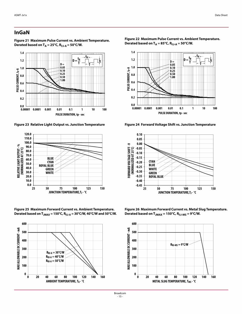
InGaNFigure 21 Maximum Pulse Current vs. Ambient Temperature. Derated based on TA = 25°C, RJ-A = 50°C/W.
Figure 22 Maximum Pulse Current vs. Ambient Temperature. Derated based on TA = 85°C, RJ-A = 50°C/W.
0.0
0.2
0.4
0.6
0.8
1.0
1.2
1.4
0.00001 0.0001 0.001 0.01 0.1 1 10 100
PULS
E CUR
RENT
, IP-A
PULSE DURATION, tp - sec
D =0.050.100.250.501.00
D = tpT
tpIF
T
0.0
0.2
0.4
0.6
0.8
1.0
1.2
1.4
0.00001 0.0001 0.001 0.01 0.1 1 10 100PULSE DURATION, tp - sec
PULS
E CUR
RENT
, IP-A
D =0.050.100.250.501.00
D = tpT
tpIF
T
Figure 23 Relative Light Output vs. Junction Temperature Figure 24 Forward Voltage Shift vs. Junction Temperature
0.010.020.030.040.050.060.070.080.090.0
100.0110.0120.0
25 50 75 100 125 150
BLUECYAN
ROYAL BLUEGREENWHITE
RELA
TIVE
LIGH
T OUT
PUT -
%(N
ORM
ALIZ
ED A
T 25°
C)
JUNCTION TEMPERATURE,TJ - °C
-0.45-0.40-0.35-0.30-0.25-0.20-0.15-0.10-0.05
0.000.050.10
25 50 75 100 125 150
CYANBLUEWHITEGREENROYAL BLUEFO
RWAR
D VO
LTAG
E SHI
FT - V
(NOR
MAL
IZED
AT 2
5°C)
JUNCTION TEMPERATURE,TJ - °C
Figure 25 Maximum Forward Current vs. Ambient Temperature. Derated based on TJMAX = 150°C, RJ-A = 30°C/W, 40°C/W and 50°C/W.
Figure 26 Maximum Forward Current vs. Metal Slug Temperature. Derated based on TJMAX = 150°C, RJ-MS = 9°C/W.
AMBIENT TEMPERATURE, TA - °C
0
100
200
300
400
500
600
0 20 40 60 80 100 120 140 160
MAX
ALL
OWAB
LE D
C CUR
RENT
- mA
RθJ-A = 30°C/WRθJ-A = 40°C/WRθJ-A = 50°C/W
METAL SLUG TEMPERATURE, TMS - °C
0
100
200
300
400
500
600
0 20 40 60 80 100 120 140 160
MAX
ALL
OWAB
LE D
C CUR
RENT
- mA
RθJ-MS = 9°C/W
Broadcom- 15 -
ASMT-Jx1x Data Sheet
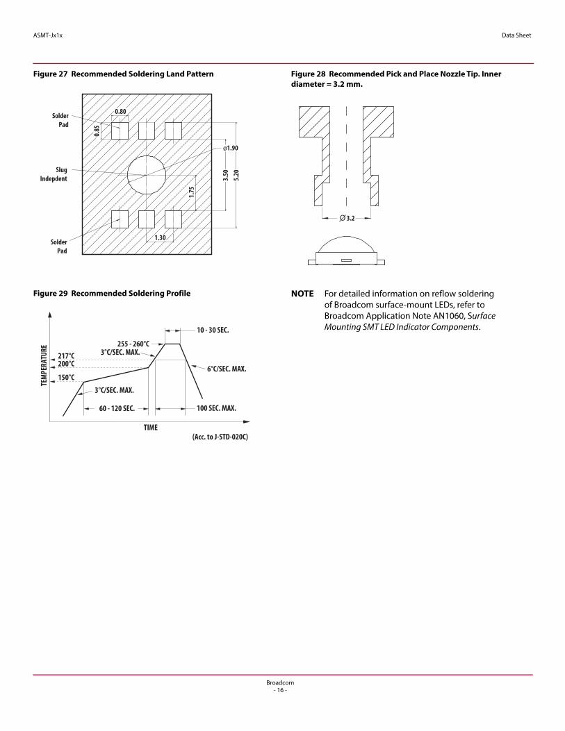
Figure 27 Recommended Soldering Land Pattern Figure 28 Recommended Pick and Place Nozzle Tip. Inner diameter = 3.2 mm.
SolderPad
SolderPad
SlugIndepdent
0.80
0.85
1.75
1.30
ø1.90
3.50
5.20
O 3.2
Figure 29 Recommended Soldering Profile NOTE For detailed information on reflow soldering of Broadcom surface-mount LEDs, refer to Broadcom Application Note AN1060, Surface Mounting SMT LED Indicator Components.
(Acc. to J-STD-020C)
217°C200°C
60 - 120 SEC.
6°C/SEC. MAX.
3°C/SEC. MAX.
3°C/SEC. MAX.
150°C
255 - 260°C
100 SEC. MAX.
10 - 30 SEC.
TIME
TEM
PERA
TURE
Broadcom- 16 -
ASMT-Jx1x Data Sheet
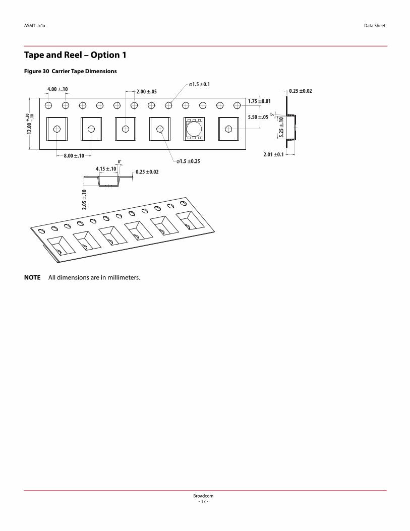
Tape and Reel – Option 1
Figure 30 Carrier Tape Dimensions
NOTE All dimensions are in millimeters.
4.00 ±.10
8.00 ±.10
12.0
0+.
30–.
10
4.15 ±.10 0.25 ±0.02
2.05
±.1
0
8° ø1.5 ±0.25
2.00 ±.05
5.50 ±.05
1.75 ±0.01
0.25 ±0.02
2.01 ±0.1
ø1.5 ±0.1
5°
5.25
±.1
0
Broadcom- 17 -
ASMT-Jx1x Data Sheet
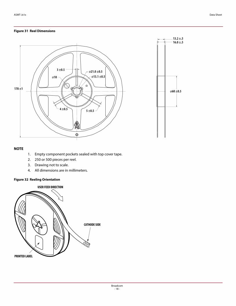
Figure 31 Reel Dimensions
NOTE1. Empty component pockets sealed with top cover tape.2. 250 or 500 pieces per reel.3. Drawing not to scale.4. All dimensions are in millimeters.
Figure 32 Reeling Orientation
178 ±1
4 ±0.5 5 ±0.5
3 ±0.5 ø21.0 ±0.5
ø10 ø13.1 ±0.5
ø60 ±0.5
13.2 ±.516.0 ±.5
CATHODE SIDE
USER FEED DIRECTION
PRINTED LABEL
Broadcom- 18 -

DISCLAIMER: Broadcom’s products and software are not specifically designed, manufactured, or authorized for sale as parts, components, or assemblies for the planning, construction, maintenance, or direct operation of a nuclear facility or for use in medical devices or applications. The customer is solely responsible, and waives all rights to make claims against Broadcom or its suppliers, for all loss, damage, expense, or liability in connection with such use.
For product information and a complete list of distributors, please go to our web site: www.broadcom.com.
Broadcom, the pulse logo, Connecting everything, Avago Technologies, Avago, and the A logo are among the trademarks of Broadcom and/or its affiliates in the United States, certain other countries and/or the EU.
Copyright © 2015–2017 by Broadcom. All Rights Reserved.
The term "Broadcom" refers to Broadcom Limited and/or its subsidiaries. For more information, please visit www.broadcom.com.
Broadcom reserves the right to make changes without further notice to any products or data herein to improve reliability, function, or design.
Information furnished by Broadcom is believed to be accurate and reliable. However, Broadcom does not assume any liability arising out of the application or use of this information, nor the application or use of any product or circuit described herein, neither does it convey any license under its patent rights nor the rights of others.
AV02-1770EN – May 5, 2017