Embed Size (px)
Citation preview
Jan. 21, 2003Jan. 21, 2003
ASPDAC Tutorial:ASPDAC Tutorial:Power, Timing & Signal Integrity Power, Timing & Signal Integrity
in in SoCSoC designsdesignsSection IISection II
Eli ChiproutEli ChiproutStrategic CAD, Intel LabsStrategic CAD, Intel Labs
Chandler AZChandler AZelieli..chiproutchiprout@@intelintel.com.com
Jan. 21, 2003Jan. 21, 2003 ASPDAC Tutorial: Power, Timing & S.I.ASPDAC Tutorial: Power, Timing & S.I. 22
Eli ChiproutStrategic CAD, Intel Labs
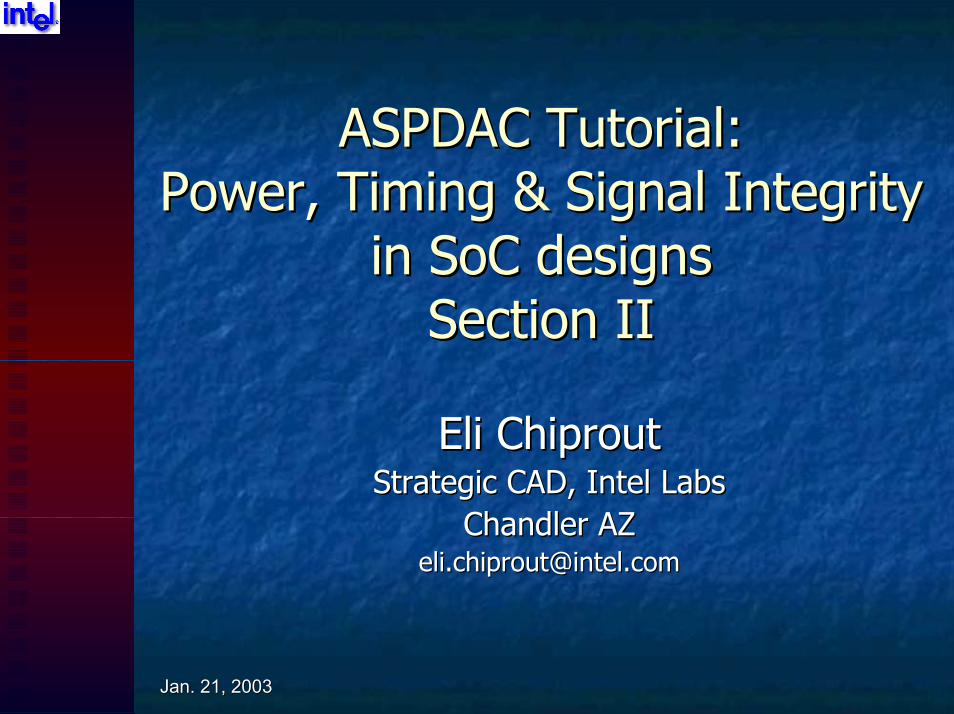
Section II: Modeling, noise, timingSection II: Modeling, noise, timing
The goals of this section is toThe goals of this section is to::Introduce scaling and the impact on modelsIntroduce scaling and the impact on models
Discuss the “interconnect problem”Discuss the “interconnect problem”
Timing, noise, noise on timingTiming, noise, noise on timing
Give types of models usedGive types of models used
Delay modelsDelay models
Moment modelsMoment models
PEEC modelsPEEC models
Show inductance effects onShow inductance effects on--chipchip
Impact on modelingImpact on modeling
Discuss model reductionDiscuss model reduction
Jan. 21, 2003Jan. 21, 2003 ASPDAC Tutorial: Power, Timing & S.I.ASPDAC Tutorial: Power, Timing & S.I. 33
Eli ChiproutStrategic CAD, Intel Labs
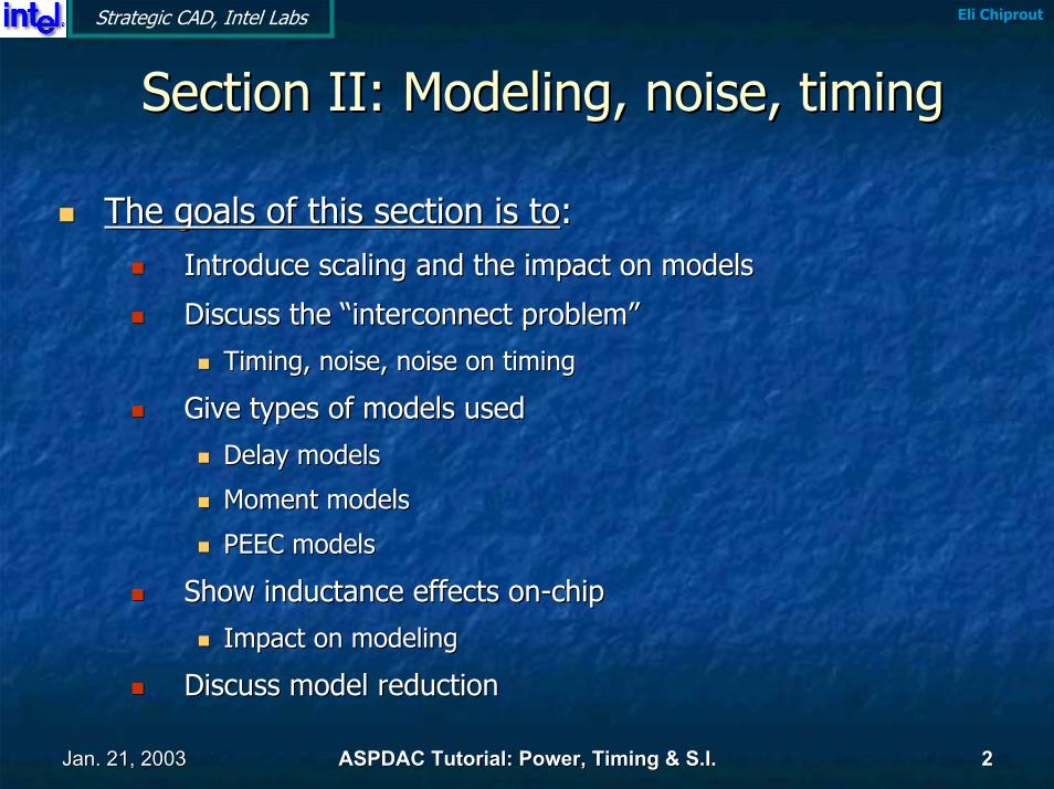
Design Paradigm ShiftDesign Paradigm Shift
CircuitCircuit--centriccentricCircuit poses major Circuit poses major constraintsconstraintsSlower convergence when Slower convergence when interconnects weigh moreinterconnects weigh more
InterconnectInterconnectCentricCentric
CircuitCircuitCentricCentric
InterconnectInterconnect--centriccentricInterconnect dominatedInterconnect dominatedCircuit built around Circuit built around interconnectsinterconnects
Jan. 21, 2003Jan. 21, 2003 ASPDAC Tutorial: Power, Timing & S.I.ASPDAC Tutorial: Power, Timing & S.I. 44
Eli ChiproutStrategic CAD, Intel Labs
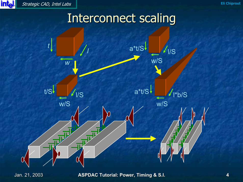
Interconnect scalingInterconnect scaling
t/S
w/Sl/S a*t/S
w/Sl*b/S
w
tl a*t/S
w/Sl/S
Jan. 21, 2003Jan. 21, 2003 ASPDAC Tutorial: Power, Timing & S.I.ASPDAC Tutorial: Power, Timing & S.I. 55
Eli ChiproutStrategic CAD, Intel Labs
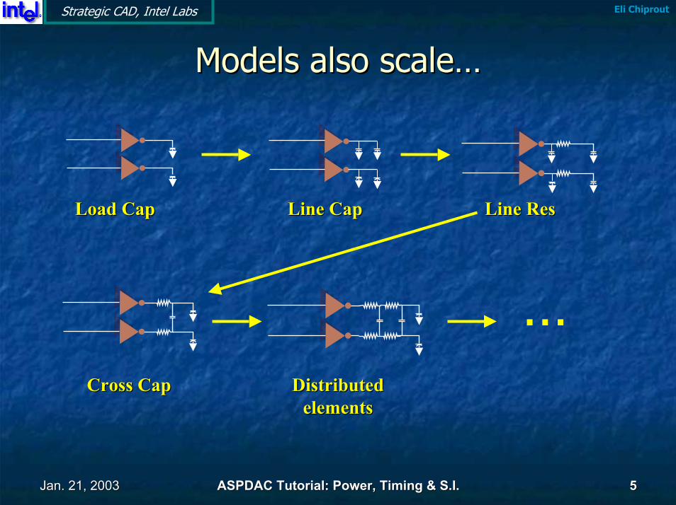
Models also scale…Models also scale…
Line CapLine CapLoad CapLoad Cap Line Line ResRes
…Cross CapCross Cap Distributed Distributed
elementselements
Jan. 21, 2003Jan. 21, 2003 ASPDAC Tutorial: Power, Timing & S.I.ASPDAC Tutorial: Power, Timing & S.I. 66
Eli ChiproutStrategic CAD, Intel Labs
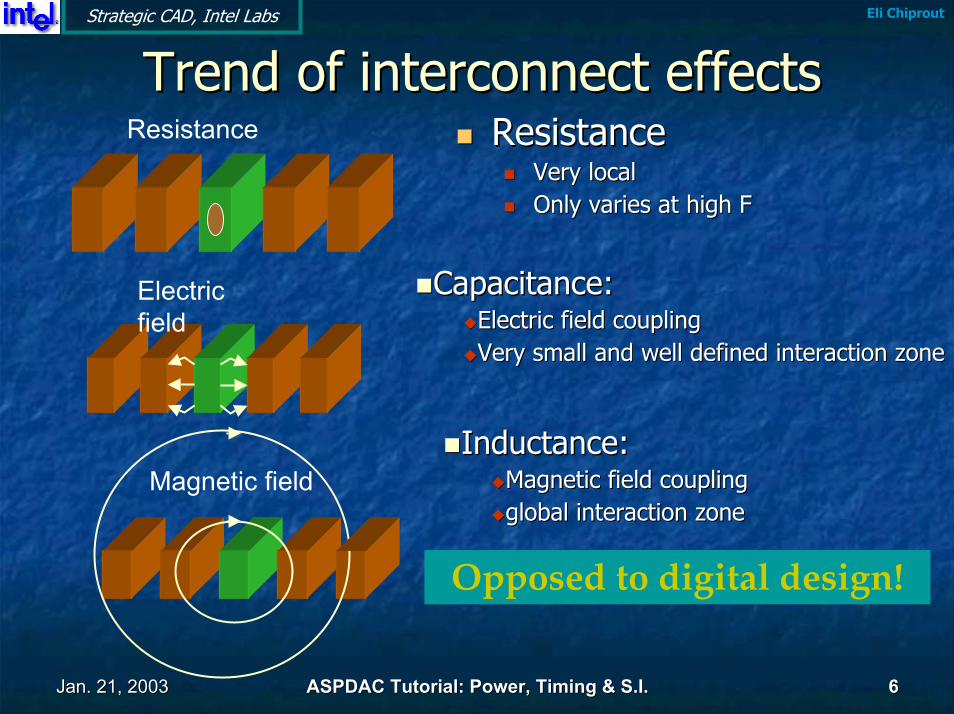
Trend of interconnect effectsTrend of interconnect effectsResistanceResistance
Very localVery localOnly varies at high F
Resistance
Only varies at high F
Capacitance:Capacitance:Electric field coupling Electric field coupling Very small and well defined interaction zone
Electric field
Very small and well defined interaction zone
Inductance:Inductance:Magnetic field coupling Magnetic field coupling global interaction zone
Magnetic fieldglobal interaction zone
Opposed to digital design!
Jan. 21, 2003Jan. 21, 2003 ASPDAC Tutorial: Power, Timing & S.I.ASPDAC Tutorial: Power, Timing & S.I. 77
Eli ChiproutStrategic CAD, Intel Labs
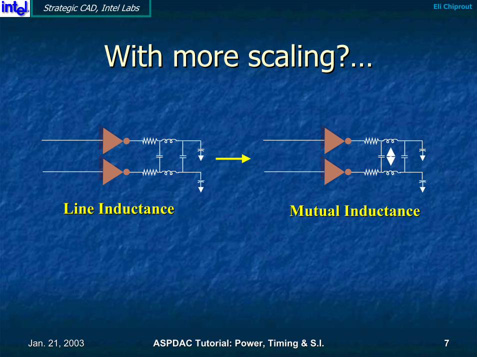
With more scaling?…With more scaling?…
Line InductanceLine Inductance Mutual InductanceMutual Inductance
Jan. 21, 2003Jan. 21, 2003 ASPDAC Tutorial: Power, Timing & S.I.ASPDAC Tutorial: Power, Timing & S.I. 88
Eli ChiproutStrategic CAD, Intel Labs
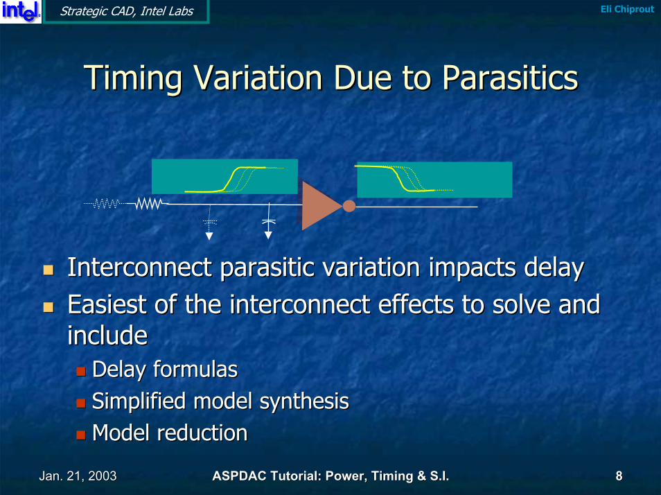
Timing Variation Due to ParasiticsTiming Variation Due to Parasitics
TFMAX
Interconnect parasitic variation impacts delayInterconnect parasitic variation impacts delayEasiest of the interconnect effects to solve and Easiest of the interconnect effects to solve and include include
Delay formulasDelay formulasSimplified model synthesisSimplified model synthesisModel reductionModel reduction
Jan. 21, 2003Jan. 21, 2003 ASPDAC Tutorial: Power, Timing & S.I.ASPDAC Tutorial: Power, Timing & S.I. 99
Eli ChiproutStrategic CAD, Intel Labs
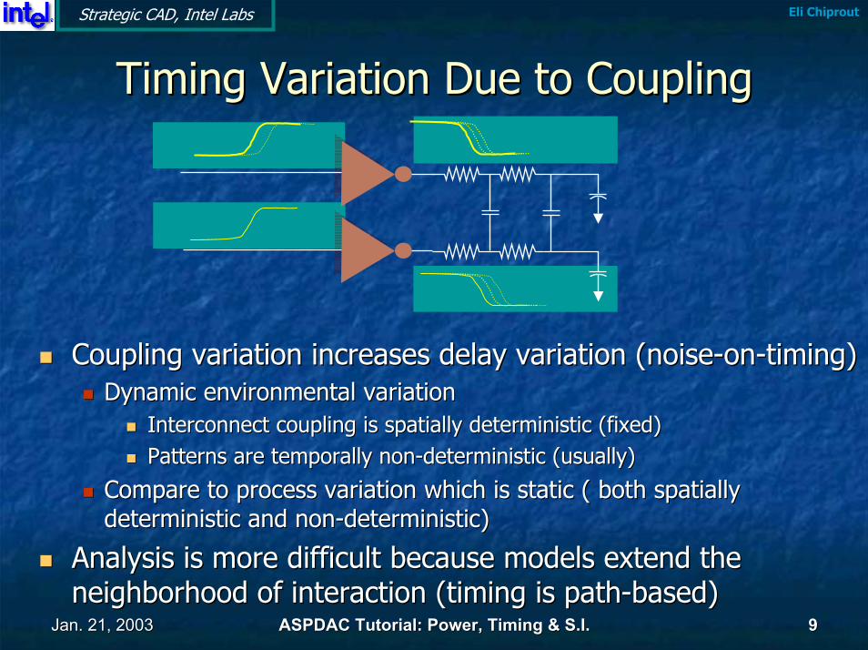
Timing Variation Due to CouplingTiming Variation Due to CouplingTF
MAX
Coupling variation increases delay variation (noiseCoupling variation increases delay variation (noise--onon--timing)timing)Dynamic environmental variationDynamic environmental variation
Interconnect coupling is spatially deterministic (fixed)Interconnect coupling is spatially deterministic (fixed)Patterns are temporally nonPatterns are temporally non--deterministic (usually)deterministic (usually)
Compare to process variation which is static ( both spatially Compare to process variation which is static ( both spatially deterministic and nondeterministic and non--deterministic)deterministic)
Analysis is more difficult because models extend the Analysis is more difficult because models extend the neighborhood of interaction (timing is pathneighborhood of interaction (timing is path--based)based)
Jan. 21, 2003Jan. 21, 2003 ASPDAC Tutorial: Power, Timing & S.I.ASPDAC Tutorial: Power, Timing & S.I. 1010
Eli ChiproutStrategic CAD, Intel Labs
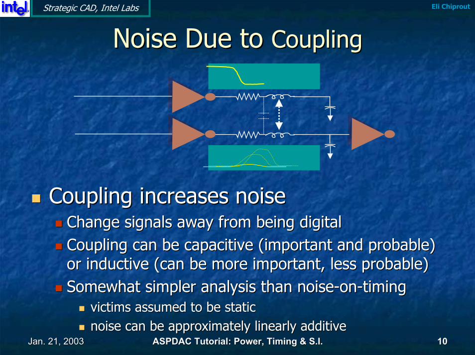
Noise Due to Noise Due to CouplingCouplingTF
MAX
Coupling increases noiseCoupling increases noiseChange signals away from being digitalChange signals away from being digitalCoupling can be capacitive (important and probable) Coupling can be capacitive (important and probable) or inductive (can be more important, less probable)or inductive (can be more important, less probable)Somewhat simpler analysis than noiseSomewhat simpler analysis than noise--onon--timingtiming
victims assumed to be staticvictims assumed to be staticnoise can be approximately linearly additivenoise can be approximately linearly additive
Jan. 21, 2003Jan. 21, 2003 ASPDAC Tutorial: Power, Timing & S.I.ASPDAC Tutorial: Power, Timing & S.I. 1111
Eli ChiproutStrategic CAD, Intel Labs
ChipChip--level designlevel design
Increasing effects on delay, timing and noiseIncreasing effects on delay, timing and noise--onon--timing timing from electric fields from electric fields Design has become increasingly interconnectDesign has become increasingly interconnect--heavyheavy
R(L)C Interconnects form the majority of models and flood our R(L)C Interconnects form the majority of models and flood our design databases with 1,000,000’s of elements!design databases with 1,000,000’s of elements!
Need to understand the modeling and when it is needed Need to understand the modeling and when it is needed and when it is notand when it is not
Jan. 21, 2003Jan. 21, 2003 ASPDAC Tutorial: Power, Timing & S.I.ASPDAC Tutorial: Power, Timing & S.I. 1212
Eli ChiproutStrategic CAD, Intel Labs
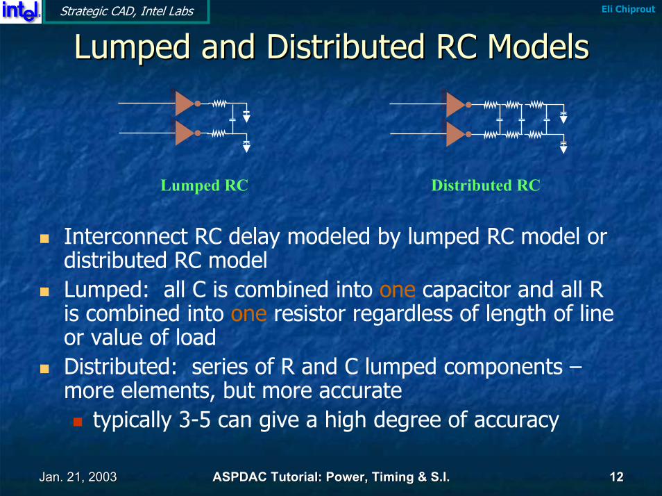
Lumped and Distributed RC ModelsLumped and Distributed RC Models
Interconnect RC delay modeled by lumped RC model or distributed RC model Lumped: all C is combined into one capacitor and all R is combined into one resistor regardless of length of line or value of loadDistributed: series of R and C lumped components –more elements, but more accurate
typically 3-5 can give a high degree of accuracy
Lumped RC Distributed RC
Jan. 21, 2003Jan. 21, 2003 ASPDAC Tutorial: Power, Timing & S.I.ASPDAC Tutorial: Power, Timing & S.I. 1313
Eli ChiproutStrategic CAD, Intel Labs
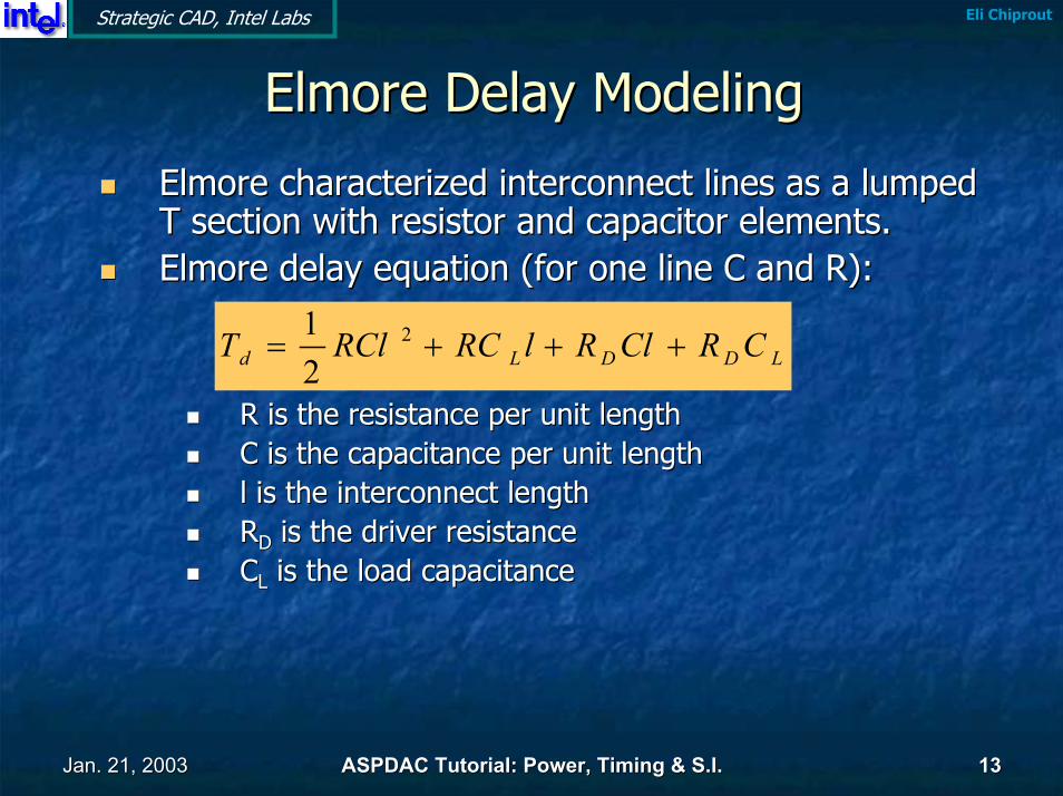
Elmore Delay ModelingElmore Delay Modeling
Elmore characterized interconnect lines as a lumped Elmore characterized interconnect lines as a lumped T section with resistor and capacitor elements.T section with resistor and capacitor elements.Elmore delay equation (for one line C and R):Elmore delay equation (for one line C and R):
R is the resistance per unit lengthR is the resistance per unit lengthC is the capacitance per unit lengthC is the capacitance per unit lengthl is the interconnect lengthl is the interconnect lengthRRDD is the driver resistanceis the driver resistanceCCLL is the load capacitanceis the load capacitance
LDDLd CRClRlRCRClT +++= 2
21
Jan. 21, 2003Jan. 21, 2003 ASPDAC Tutorial: Power, Timing & S.I.ASPDAC Tutorial: Power, Timing & S.I. 1414
Eli ChiproutStrategic CAD, Intel Labs
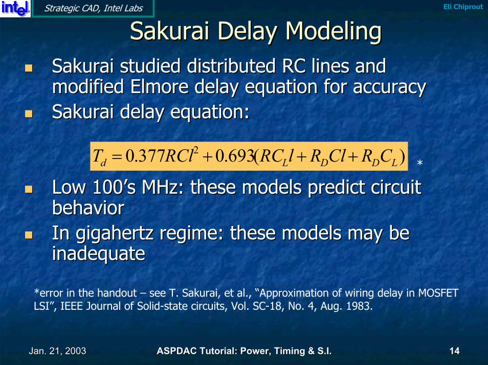
Sakurai Delay ModelingSakurai Delay ModelingSakurai studied distributed RC lines and Sakurai studied distributed RC lines and modified Elmore delay equation for accuracymodified Elmore delay equation for accuracySakurai delay equation:Sakurai delay equation:
Low 100’s MHz: these models predict circuit Low 100’s MHz: these models predict circuit behaviorbehaviorIn gigahertz regime: these models may be In gigahertz regime: these models may be inadequate
)(693.0377.0 2LDDLd CRClRlRCRClT +++= *
inadequate
*error in the handout – see T. Sakurai, et al., “Approximation of wiring delay in MOSFET LSI”, IEEE Journal of Solid-state circuits, Vol. SC-18, No. 4, Aug. 1983.
Jan. 21, 2003Jan. 21, 2003 ASPDAC Tutorial: Power, Timing & S.I.ASPDAC Tutorial: Power, Timing & S.I. 1515
Eli ChiproutStrategic CAD, Intel Labs
RC Parasitics at Medium FrequenciesRC Parasitics at Medium Frequencies
Low frequencies, skin effect on resistance negligible Low frequencies, skin effect on resistance negligible -- R R considered frequency independent.considered frequency independent.
If R >> If R >> ωωL, L neglected and RC model adequate L, L neglected and RC model adequate R is interconnect resistanceR is interconnect resistanceL is interconnect inductanceL is interconnect inductanceωω is operating frequencyis operating frequency
Smaller features and higher frequencies Smaller features and higher frequencies -- R and C R and C affected by technology scaling in relation to line width.affected by technology scaling in relation to line width.
Jan. 21, 2003Jan. 21, 2003 ASPDAC Tutorial: Power, Timing & S.I.ASPDAC Tutorial: Power, Timing & S.I. 1616
Eli ChiproutStrategic CAD, Intel Labs
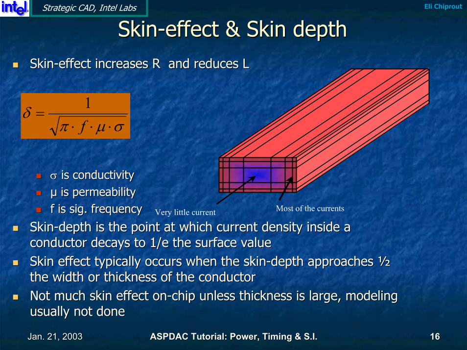
SkinSkin--effect & Skin deptheffect & Skin depthSkinSkin--effect increases R and reduces Leffect increases R and reduces L
σσ is conductivityis conductivityµ is permeabilityµ is permeabilityf is sig. frequencyf is sig. frequency
SkinSkin--depth is the point at which current density inside a depth is the point at which current density inside a conductor decays to 1/e the surface valueconductor decays to 1/e the surface valueSkin effect typically occurs when the skinSkin effect typically occurs when the skin--depth approaches ½ depth approaches ½ the width or thickness of the conductorthe width or thickness of the conductorNot much skin effect onNot much skin effect on--chip unless thickness is large, modeling chip unless thickness is large, modeling usually not doneusually not done
Very little current Most of the currents
σµπδ
⋅⋅⋅=
f1
Jan. 21, 2003Jan. 21, 2003 ASPDAC Tutorial: Power, Timing & S.I.ASPDAC Tutorial: Power, Timing & S.I. 1717
Eli ChiproutStrategic CAD, Intel Labs
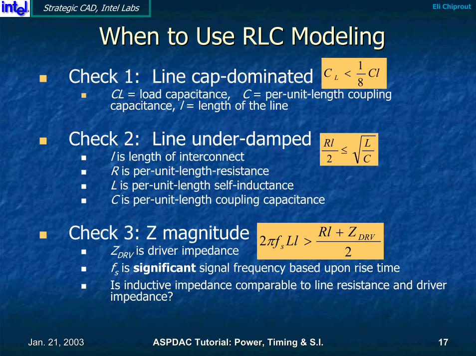
When to Use RLC ModelingWhen to Use RLC Modeling
Check 1: Line cap-dominated CL = load capacitance, C = per-unit-length coupling capacitance, l = length of the line
Check 2: Line under-dampedl is length of interconnectR is per-unit-length-resistanceL is per-unit-length self-inductanceC is per-unit-length coupling capacitance
Check 3: Z magnitudeZDRV is driver impedancefs is significant signal frequency based upon rise time Is inductive impedance comparable to line resistance and driver impedance?
ClC L 81
<
CLRl
≤2
22 DRV
sZRlLlf +
>π
Jan. 21, 2003Jan. 21, 2003 ASPDAC Tutorial: Power, Timing & S.I.ASPDAC Tutorial: Power, Timing & S.I. 1818
Eli ChiproutStrategic CAD, Intel Labs
MultiMulti--conductor RLC Modelingconductor RLC Modeling
In general interconnects & power delivery systems with In general interconnects & power delivery systems with N number of conductors can be modeled using a system N number of conductors can be modeled using a system of of NxNNxN RLC matricesRLC matricesFor each interconnect line, a corresponding row and For each interconnect line, a corresponding row and column exists in the [R] matrix, [L] matrix, and [C] column exists in the [R] matrix, [L] matrix, and [C] matrix.matrix.
G matrix is generally neglected in Z=(R+G matrix is generally neglected in Z=(R+sLsL)/(G+)/(G+sCsC))
The offThe off--diagonal terms represent the interaction or diagonal terms represent the interaction or coupling between two interconnectscoupling between two interconnectsA complete set of matrices (RLC) can be extracted for A complete set of matrices (RLC) can be extracted for any given frequency by 2D EM modelingany given frequency by 2D EM modeling
Jan. 21, 2003Jan. 21, 2003 ASPDAC Tutorial: Power, Timing & S.I.ASPDAC Tutorial: Power, Timing & S.I. 1919
Eli ChiproutStrategic CAD, Intel Labs
Why MultiWhy Multi--conductor RLC Modeling?conductor RLC Modeling?
MultiMulti--conductor modeling is expensive to use conductor modeling is expensive to use but always accuratebut always accurateFor some n wire structures, the return path For some n wire structures, the return path assumption can be applied to reduce to nassumption can be applied to reduce to n--11Typically used for board level but also for Typically used for board level but also for detailed understanding (not fulldetailed understanding (not full--chip flows)chip flows)Common applications:Common applications:
To analyze detailed noise coupling between groups To analyze detailed noise coupling between groups of signals that switch simultaneously (i.e., a bus)of signals that switch simultaneously (i.e., a bus)To analyze VTo analyze VCCCC & V& VSSSS return effectsreturn effects
Jan. 21, 2003Jan. 21, 2003 ASPDAC Tutorial: Power, Timing & S.I.ASPDAC Tutorial: Power, Timing & S.I. 2020
Eli ChiproutStrategic CAD, Intel Labs
Why think about inductance?Why think about inductance?NEW TECHNOLOGYNEW TECHNOLOGY
Fast switching timesEvery pico-second is important in fast designs pushing limits
SILICONSILICON observationsobservationsDivergence between silicon measurements and RC modelsDivergence between silicon measurements and RC modelsHP documented uP silicon failure due to inductanceHP documented uP silicon failure due to inductance
SIMULATIONSIMULATION observationsobservationsNoise difference between RC and RLC modelsNoise difference between RC and RLC modelsTiming difference between RC and RCL modelsTiming difference between RC and RCL modelsSkew difference between RC and RLC modelsSkew difference between RC and RLC models
SPEED OF LIGHTSPEED OF LIGHT limitationslimitationsWe are approaching these regimes on chip so inductive effects We are approaching these regimes on chip so inductive effects must appearmust appear
Jan. 21, 2003Jan. 21, 2003 ASPDAC Tutorial: Power, Timing & S.I.ASPDAC Tutorial: Power, Timing & S.I. 2121
Eli ChiproutStrategic CAD, Intel Labs
Primary effects of onPrimary effects of on--die inductancedie inductancePower grid noise (up to resonance): Power grid noise (up to resonance):
di/dt rapidly grows per di/dt rapidly grows per new technologynew technology
Clock skewClock skewinductance especially important due to wide wires and fast edgesinductance especially important due to wide wires and fast edges
Delay (slope at receiver end):Delay (slope at receiver end):underunder-- or overestimated if inductive coupling is ignoredor overestimated if inductive coupling is ignoredunderestimated if return path resistance is neglectedunderestimated if return path resistance is neglectedimpacts repeaters insertion methodologyimpacts repeaters insertion methodology
Propagation delay (flight time):Propagation delay (flight time):ignored (estimated as 0) if interconnect inductance is ignored;ignored (estimated as 0) if interconnect inductance is ignored;
(LC) per unit length (LC) per unit length ≥≥ µεµε = 1/v= 1/v22 , v = speed of light in matter, v = speed of light in matterSiOSiO22: : εε//εε00 = 3.5, v = 160 = 3.5, v = 160 µµm/psec, ~ 10,000 m/psec, ~ 10,000 µµm / 60 psecm / 60 psec
OvershootOvershoot--ringing:ringing:severe reliability hazardsevere reliability hazard
Mutual noise:Mutual noise:mutual inductancemutual inductance can, on low probability, be higher than crosscan, on low probability, be higher than cross--cap noisecap noise
Jan. 21, 2003Jan. 21, 2003 ASPDAC Tutorial: Power, Timing & S.I.ASPDAC Tutorial: Power, Timing & S.I. 2222
Eli ChiproutStrategic CAD, Intel Labs
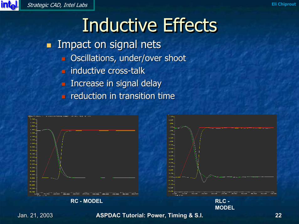
Inductive EffectsInductive EffectsInductive EffectsImpact on signal netsImpact on signal nets
Oscillations, under/over shootOscillations, under/over shootinductive crossinductive cross--talktalkIncrease in signal delayIncrease in signal delayreduction in transition timereduction in transition time
RC - MODEL RLC -MODEL
Jan. 21, 2003Jan. 21, 2003 ASPDAC Tutorial: Power, Timing & S.I.ASPDAC Tutorial: Power, Timing & S.I. 2323
Eli ChiproutStrategic CAD, Intel Labs
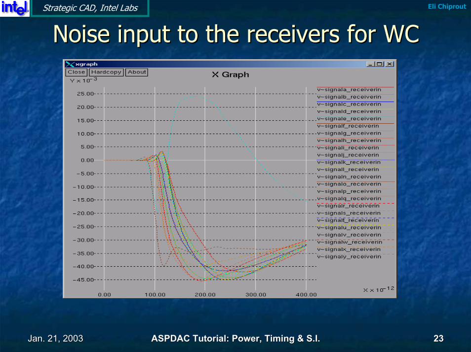
Noise input to the receivers for WCNoise input to the receivers for WC
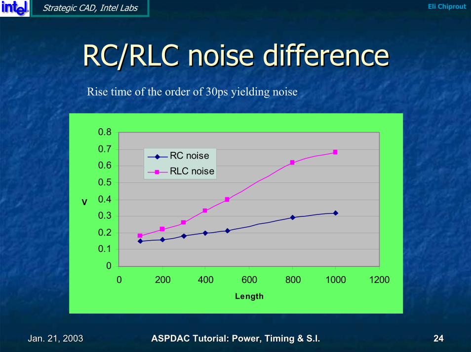
Jan. 21, 2003Jan. 21, 2003 ASPDAC Tutorial: Power, Timing & S.I.ASPDAC Tutorial: Power, Timing & S.I. 2424
Eli ChiproutStrategic CAD, Intel Labs
RC/RLC noise differenceRC/RLC noise differenceRise time of the order of 30ps yielding noise
0
0.1
0.2
0.3
0.4
0.5
0.6
0.7
0.8
0 200 400 600 800 1000 1200Length
V
RC noiseRLC noise
Jan. 21, 2003Jan. 21, 2003 ASPDAC Tutorial: Power, Timing & S.I.ASPDAC Tutorial: Power, Timing & S.I. 2525
Eli ChiproutStrategic CAD, Intel Labs
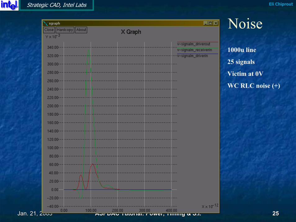
Noise1000u line
25 signals
Victim at 0V
WC RLC noise (+)
Jan. 21, 2003Jan. 21, 2003 ASPDAC Tutorial: Power, Timing & S.I.ASPDAC Tutorial: Power, Timing & S.I. 2626
Eli ChiproutStrategic CAD, Intel Labs
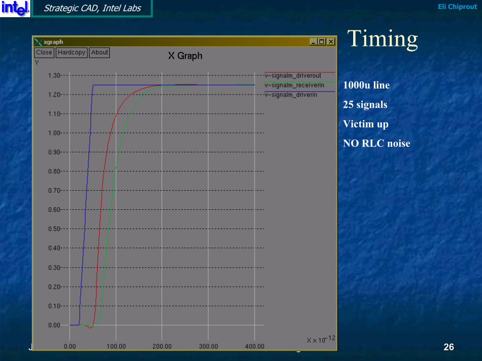
Timing
1000u line
25 signals
Victim up
NO RLC noise
Jan. 21, 2003Jan. 21, 2003 ASPDAC Tutorial: Power, Timing & S.I.ASPDAC Tutorial: Power, Timing & S.I. 2727
Eli ChiproutStrategic CAD, Intel Labs
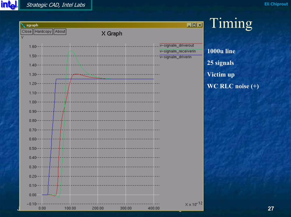
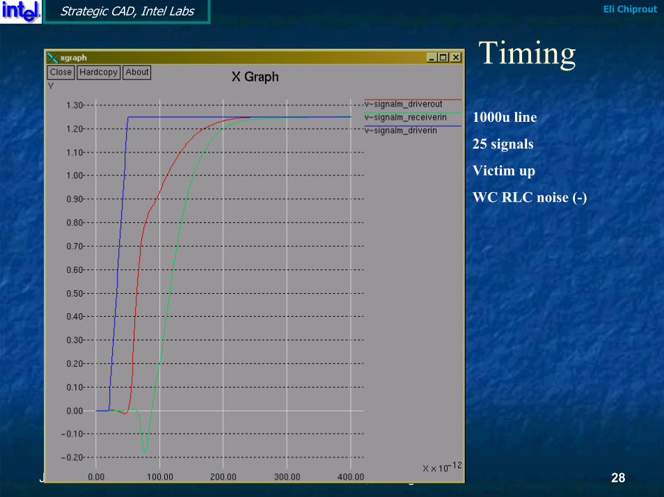
Timing
1000u line
25 signals
Victim up
WC RLC noise (+)
Jan. 21, 2003Jan. 21, 2003 ASPDAC Tutorial: Power, Timing & S.I.ASPDAC Tutorial: Power, Timing & S.I. 2828
Eli ChiproutStrategic CAD, Intel Labs
Timing
1000u line
25 signals
Victim up
WC RLC noise (-)
Jan. 21, 2003Jan. 21, 2003 ASPDAC Tutorial: Power, Timing & S.I.ASPDAC Tutorial: Power, Timing & S.I. 2929
Eli ChiproutStrategic CAD, Intel Labs
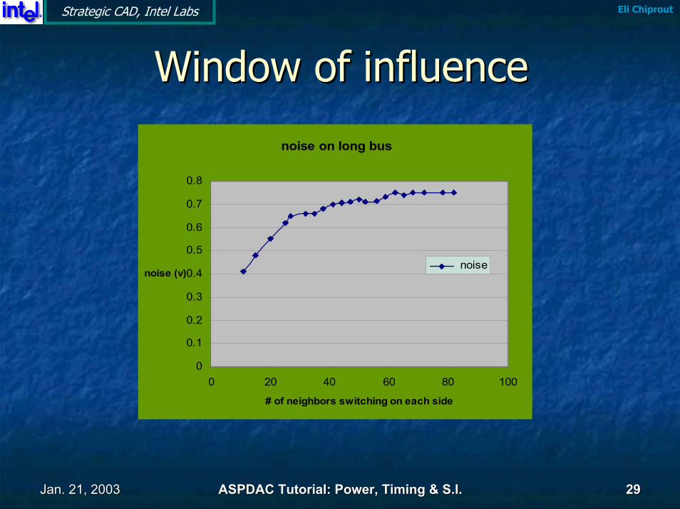
Window of influenceWindow of influence
noise on long bus
0
0.1
0.2
0.3
0.4
0.5
0.6
0.7
0.8
0 20 40 60 80 100
# of neighbors switching on each side
noise (v) noise
Jan. 21, 2003Jan. 21, 2003 ASPDAC Tutorial: Power, Timing & S.I.ASPDAC Tutorial: Power, Timing & S.I. 3030
Eli ChiproutStrategic CAD, Intel Labs
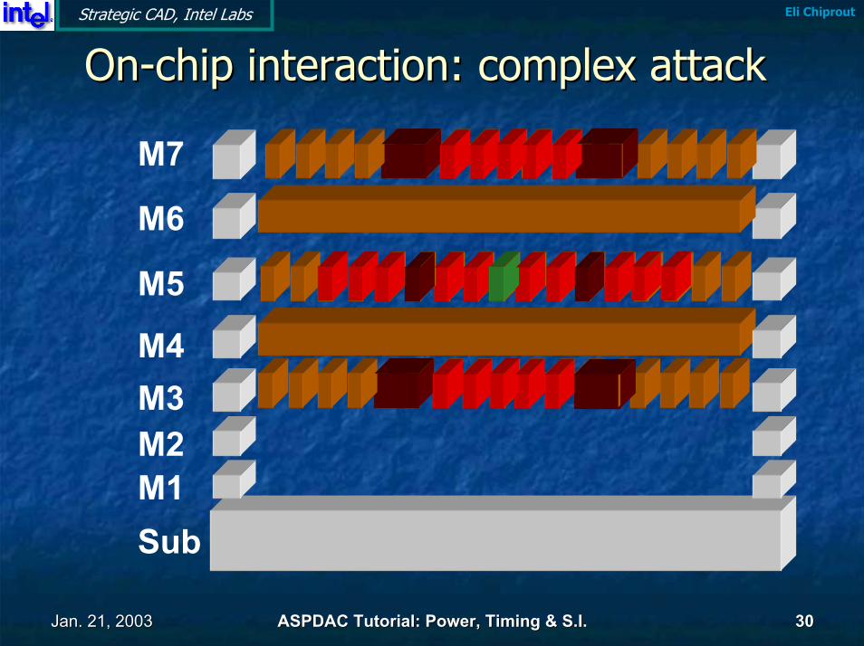
OnOn--chip interaction: complex attackchip interaction: complex attack
M5
M4M3M2M1Sub
M6
M7
Jan. 21, 2003Jan. 21, 2003 ASPDAC Tutorial: Power, Timing & S.I.ASPDAC Tutorial: Power, Timing & S.I. 3131
Eli ChiproutStrategic CAD, Intel Labs
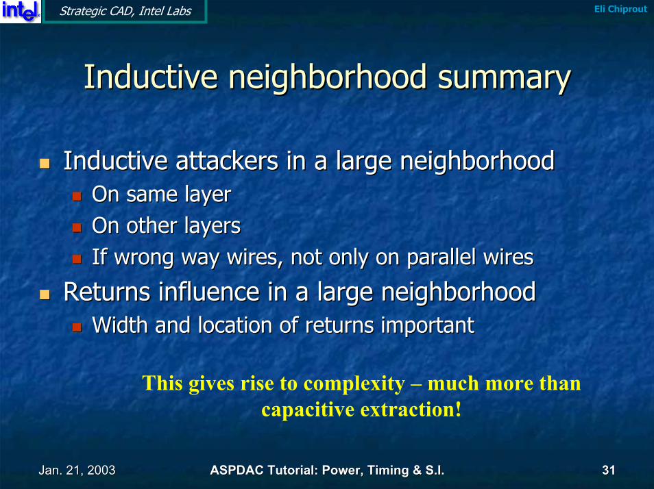
Inductive neighborhood summaryInductive neighborhood summary
Inductive attackers in a large neighborhoodInductive attackers in a large neighborhoodOn same layerOn same layerOn other layersOn other layersIf wrong way wires, not only on parallel wiresIf wrong way wires, not only on parallel wires
Returns influence in a large neighborhoodReturns influence in a large neighborhoodWidth and location of returns importantWidth and location of returns important
This gives rise to complexity – much more than capacitive extraction!
Jan. 21, 2003Jan. 21, 2003 ASPDAC Tutorial: Power, Timing & S.I.ASPDAC Tutorial: Power, Timing & S.I. 3232
Eli ChiproutStrategic CAD, Intel Labs
Multiple attackersMultiple attackersWorst case scenario is terrible!Worst case scenario is terrible!If we used this, design could not be doneIf we used this, design could not be doneProbability of worst case is almost zeroProbability of worst case is almost zeroHowever, a reasonable probability However, a reasonable probability window must be chosen by designerswindow must be chosen by designersThis choice of probability window This choice of probability window can be the source of inaccuracy can be the source of inaccuracy greater than inductive modeling!greater than inductive modeling!Complexity Complexity –– not accuracy.not accuracy.
Jan. 21, 2003Jan. 21, 2003 ASPDAC Tutorial: Power, Timing & S.I.ASPDAC Tutorial: Power, Timing & S.I. 3333
Eli ChiproutStrategic CAD, Intel Labs
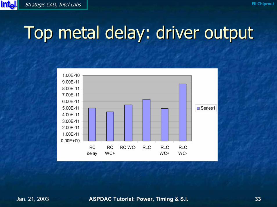
Top metal delay: driver outputTop metal delay: driver output
0.00E+001.00E-112.00E-113.00E-114.00E-115.00E-116.00E-117.00E-118.00E-119.00E-111.00E-10
RCdelay
RCWC+
RC WC- RLC RLCWC+
RLCWC-
Series1
Jan. 21, 2003Jan. 21, 2003 ASPDAC Tutorial: Power, Timing & S.I.ASPDAC Tutorial: Power, Timing & S.I. 3434
Eli ChiproutStrategic CAD, Intel Labs
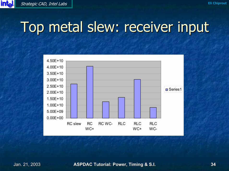
Top metal slew: receiver inputTop metal slew: receiver input
0.00E+005.00E+091.00E+101.50E+102.00E+102.50E+103.00E+103.50E+104.00E+104.50E+10
RC slew RCWC+
RC WC- RLC RLCWC+
RLCWC-
Series1
Jan. 21, 2003Jan. 21, 2003 ASPDAC Tutorial: Power, Timing & S.I.ASPDAC Tutorial: Power, Timing & S.I. 3535
Eli ChiproutStrategic CAD, Intel Labs
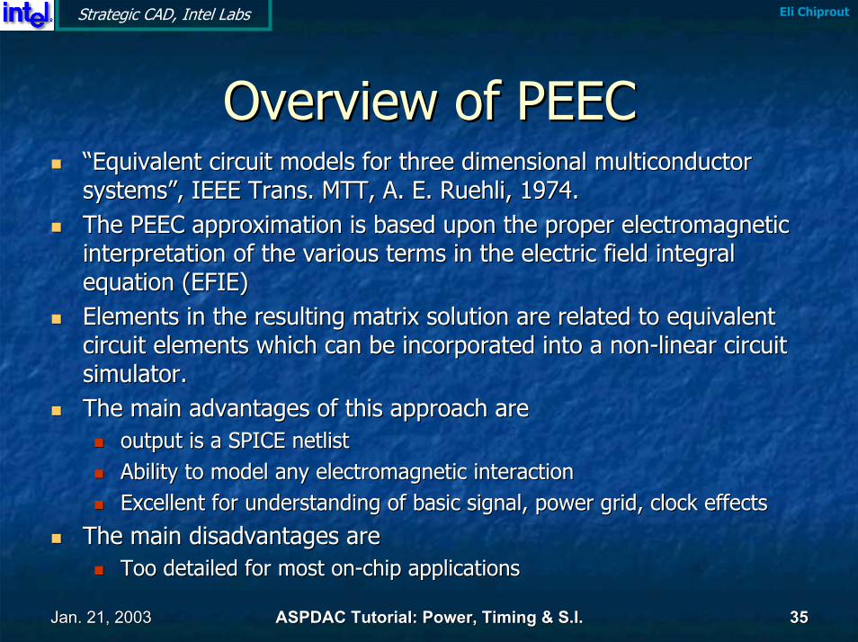
Overview of PEECOverview of PEEC“Equivalent circuit models for three dimensional “Equivalent circuit models for three dimensional multiconductormulticonductorsystems”, IEEE Trans. MTT, A. E. Ruehli, 1974.systems”, IEEE Trans. MTT, A. E. Ruehli, 1974.The PEEC approximation is based upon the proper electromagnetic The PEEC approximation is based upon the proper electromagnetic interpretation of the various terms in the electric field integrinterpretation of the various terms in the electric field integral al equation (EFIE)equation (EFIE)Elements in the resulting matrix solution are related to equivalElements in the resulting matrix solution are related to equivalent ent circuit elements which can be incorporated into a noncircuit elements which can be incorporated into a non--linear circuit linear circuit simulator.simulator.The main advantages of this approach areThe main advantages of this approach are
output is a SPICE output is a SPICE netlistnetlistAbility to model any electromagnetic interactionAbility to model any electromagnetic interactionExcellent for understanding of basic signal, power grid, clock eExcellent for understanding of basic signal, power grid, clock effectsffects
The main disadvantages areThe main disadvantages areToo detailed for most onToo detailed for most on--chip applicationschip applications
Jan. 21, 2003Jan. 21, 2003 ASPDAC Tutorial: Power, Timing & S.I.ASPDAC Tutorial: Power, Timing & S.I. 3636
Eli ChiproutStrategic CAD, Intel Labs
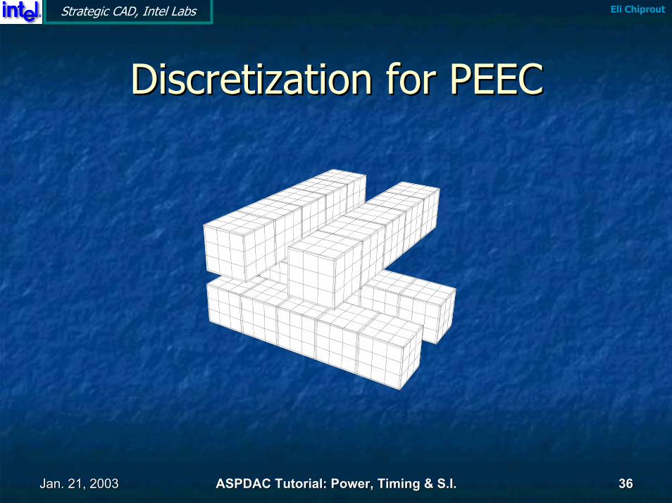
DiscretizationDiscretization for PEECfor PEEC
Jan. 21, 2003Jan. 21, 2003 ASPDAC Tutorial: Power, Timing & S.I.ASPDAC Tutorial: Power, Timing & S.I. 3737
Eli ChiproutStrategic CAD, Intel Labs
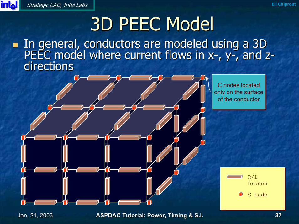
3D PEEC Model3D PEEC ModelIn general, conductors are modeled using a 3D In general, conductors are modeled using a 3D PEEC model where current flows in xPEEC model where current flows in x--, y, y--, and z, and z--directionsdirections
C nodes locatedonly on the surface
of the conductor
C nodes locatedonly on the surface
of the conductor
R/L branchC node
Jan. 21, 2003Jan. 21, 2003 ASPDAC Tutorial: Power, Timing & S.I.ASPDAC Tutorial: Power, Timing & S.I. 3838
Eli ChiproutStrategic CAD, Intel Labs
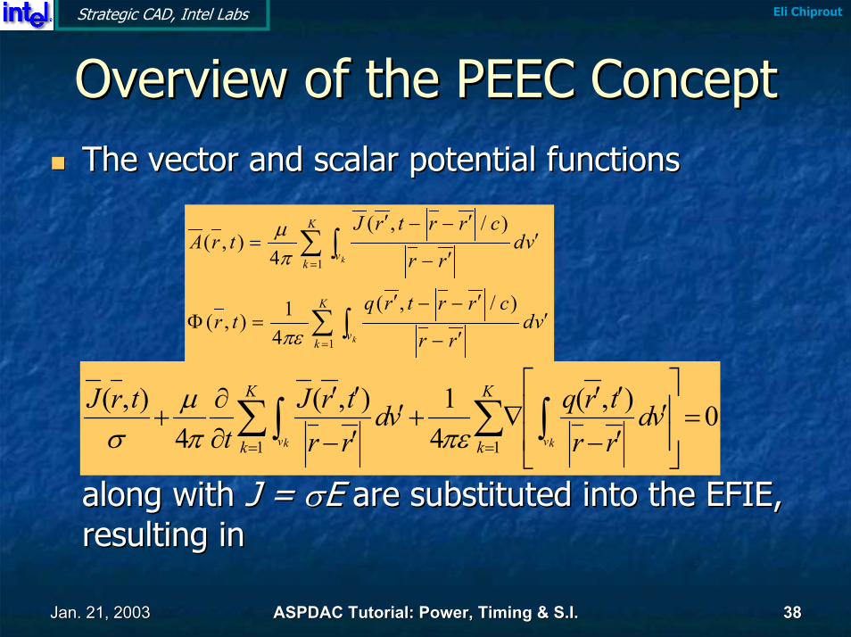
Overview of the PEEC ConceptOverview of the PEEC ConceptThe vector and scalar potential functionsThe vector and scalar potential functions
along with along with J = J = σσEE are substituted into the EFIE, are substituted into the EFIE, resulting inresulting in
∑ ∫
∑ ∫
=
=
′′−
′−−′=Φ
′′−
′−−′=
K
kv
K
kv
k
k
vdrr
crrtrqtr
vdrr
crrtrJtrA
1
1
)/,(
41),(
)/,(
4),(
πε
πµ
0),(41),(
4),(
11=
′
′−
′′∇+′
′−
′′∂∂
+ ∫∑∑∫== kvkv
vdrrtrqvd
rrtrJ
ttrJ K
k
K
k πεπµ
σ
Jan. 21, 2003Jan. 21, 2003 ASPDAC Tutorial: Power, Timing & S.I.ASPDAC Tutorial: Power, Timing & S.I. 3939
Eli ChiproutStrategic CAD, Intel Labs
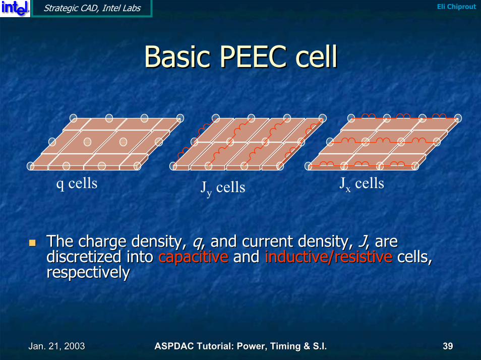
Basic PEEC cellBasic PEEC cell
q cells Jy cells Jx cells
The charge density, The charge density, qq, and current density, , and current density, JJ, are , are discretizeddiscretized into into capacitivecapacitive and and inductive/resistiveinductive/resistive cells, cells, respectivelyrespectively
Jan. 21, 2003Jan. 21, 2003 ASPDAC Tutorial: Power, Timing & S.I.ASPDAC Tutorial: Power, Timing & S.I. 4040
Eli ChiproutStrategic CAD, Intel Labs
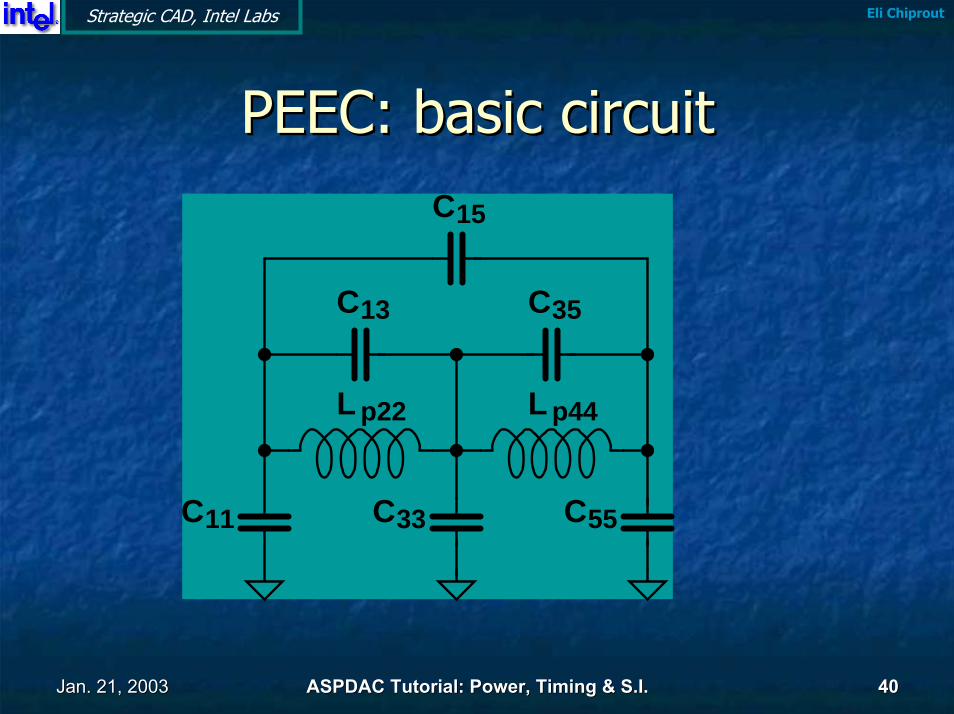
PEEC: basic circuitPEEC: basic circuit
C35
C15
C13
C55C3311C
p44p22L L
Jan. 21, 2003Jan. 21, 2003 ASPDAC Tutorial: Power, Timing & S.I.ASPDAC Tutorial: Power, Timing & S.I. 4141
Eli ChiproutStrategic CAD, Intel Labs
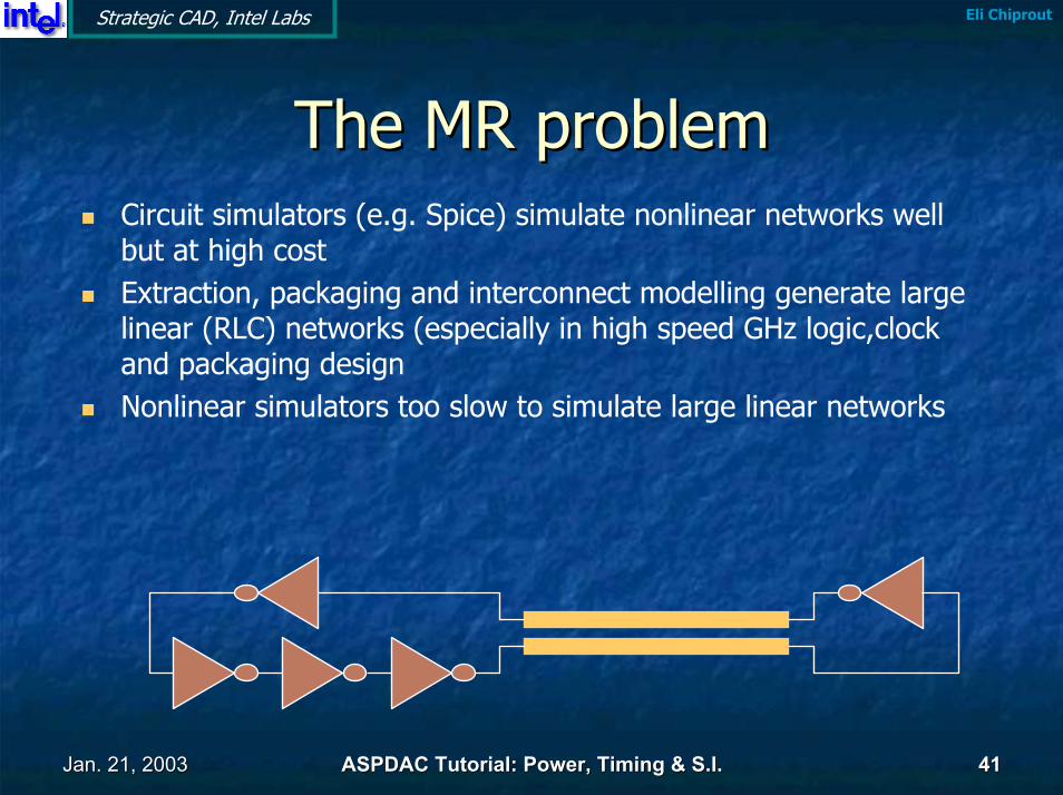
The MR problemThe MR problemCircuit simulators (e.g. Spice) simulate nonlinear networks wellbut at high costExtraction, packaging and interconnect modelling generate large linear (RLC) networks (especially in high speed GHz logic,clock and packaging designNonlinear simulators too slow to simulate large linear networks
Jan. 21, 2003Jan. 21, 2003 ASPDAC Tutorial: Power, Timing & S.I.ASPDAC Tutorial: Power, Timing & S.I. 4242
Eli ChiproutStrategic CAD, Intel Labs
MR RequirementsMR RequirementsReduce large linear networks for standalone time/frequency domain simulationReduce and macromodel large linear networks for nonlinear simulationreduction with error control, and simulation transparently to the userApplicable to on-chip logic interconnect, clock, power and gnd nets, packaging pin and interconnect modelstricky mathematical techniques necessary to accomplish this for all frequency ranges
Jan. 21, 2003Jan. 21, 2003 ASPDAC Tutorial: Power, Timing & S.I.ASPDAC Tutorial: Power, Timing & S.I. 4343
Eli ChiproutStrategic CAD, Intel Labs
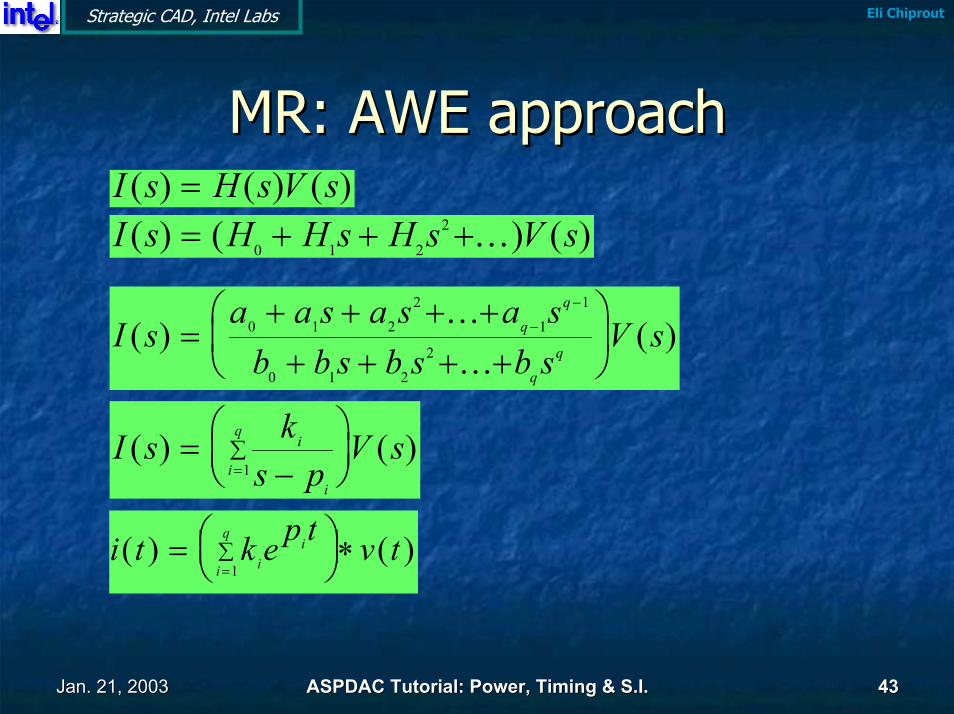
MR: AWE approachMR: AWE approachI s H s V s( ) ( ) ( )=I s H H s H s V s( ) ( ) ( )= + + +0 1 2
2 K
I sa a s a s a sb b s b s b s
V sqq
( ) ( )=+ + + ++ + + +
−
−
0 1 22
11
0 1 22
K
K
I s ks p
V si
ii
q( ) ( )=
−
=
∑1
i t k e p t v tii
i
q( ) ( )=
∗=
∑1
Jan. 21, 2003Jan. 21, 2003 ASPDAC Tutorial: Power, Timing & S.I.ASPDAC Tutorial: Power, Timing & S.I. 4444
Eli ChiproutStrategic CAD, Intel Labs
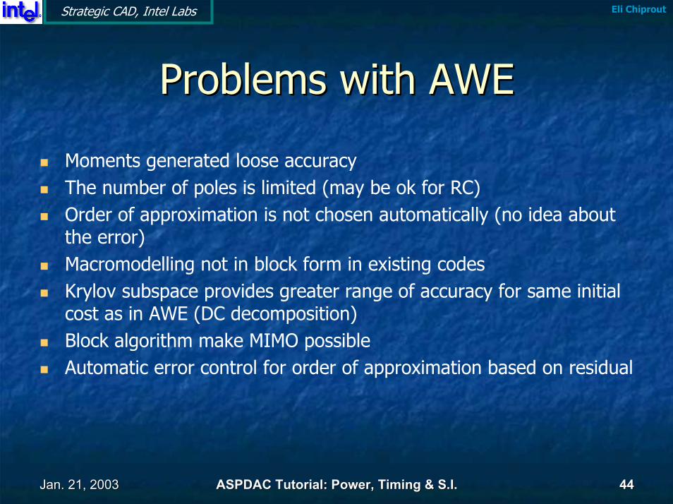
Problems with AWEProblems with AWE
Moments generated loose accuracyThe number of poles is limited (may be ok for RC)Order of approximation is not chosen automatically (no idea about the error)Macromodelling not in block form in existing codesKrylov subspace provides greater range of accuracy for same initial cost as in AWE (DC decomposition)Block algorithm make MIMO possibleAutomatic error control for order of approximation based on residual
Jan. 21, 2003Jan. 21, 2003 ASPDAC Tutorial: Power, Timing & S.I.ASPDAC Tutorial: Power, Timing & S.I. 4545
Eli ChiproutStrategic CAD, Intel Labs
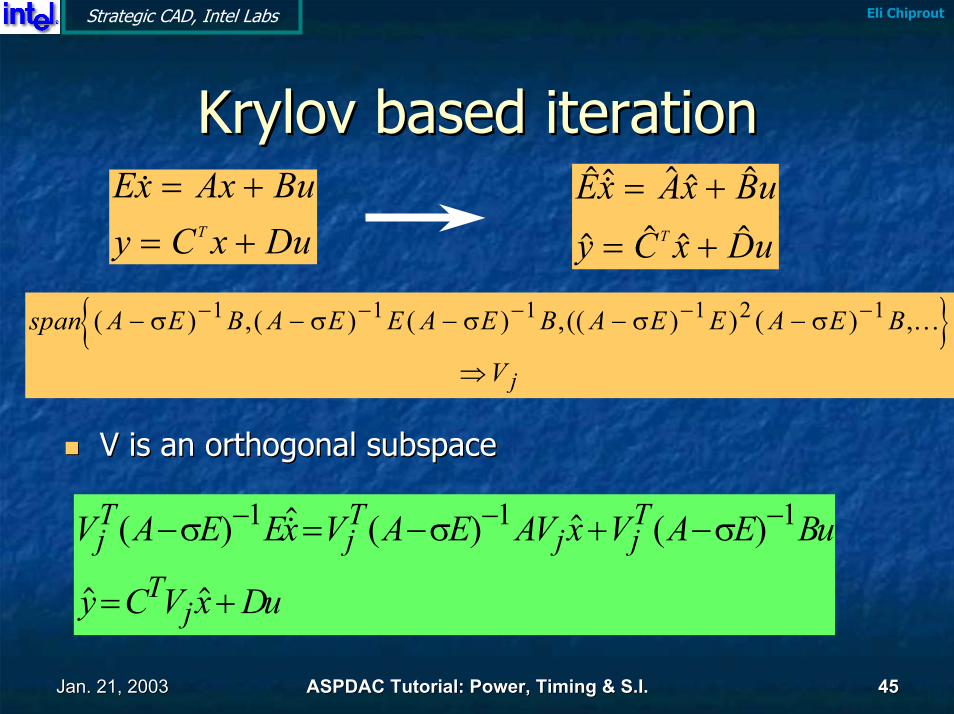
KrylovKrylov based iterationbased iteration
V is an orthogonal subspaceV is an orthogonal subspace
Ex Ax Buy C x DuT
& = += +
$ &$ $ $ $
$ $ $ $
Ex Ax Buy C x DuT
= +
= +
{ }span A E B A E E A E B A E E A E B
V j
( ) ,( ) ( ) ,(( ) ) ( ) ,− − − − −
⇒
− − − − −σ σ σ σ σ1 1 1 1 2 1 K
V A E Ex V A E AV x V A E Bu
y C V x Du
jT
jT
j jT
Tj
( ) &$ ( ) $ ( )
$ $
− = − + −
= +
− − −σ σ σ1 1 1
Jan. 21, 2003Jan. 21, 2003 ASPDAC Tutorial: Power, Timing & S.I.ASPDAC Tutorial: Power, Timing & S.I. 4646
Eli ChiproutStrategic CAD, Intel Labs
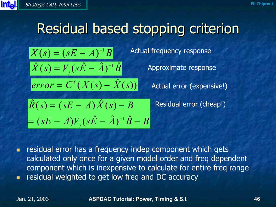
Residual based stopping criterionResidual based stopping criterionActual frequency responseX s sE A B( ) ( )= − −1
$ ( ) ( $ $ ) $X s V sE A Bj= − −1 Approximate response
error C X s X sT= −( ( ) $ ( )) Actual error (expensive!)
$ ( ) ( ) $ ( )( ) ( $ $ ) $
R s sE A X s BsE A V sE A B Bj
= − −
= − − −−1
Residual error (cheap!)
residual error has a frequency indep component which gets calculated only once for a given model order and freq dependent component which is inexpensive to calculate for entire freq rangeresidual weighted to get low freq and DC accuracy
Jan. 21, 2003Jan. 21, 2003 ASPDAC Tutorial: Power, Timing & S.I.ASPDAC Tutorial: Power, Timing & S.I. 4747
Eli ChiproutStrategic CAD, Intel Labs
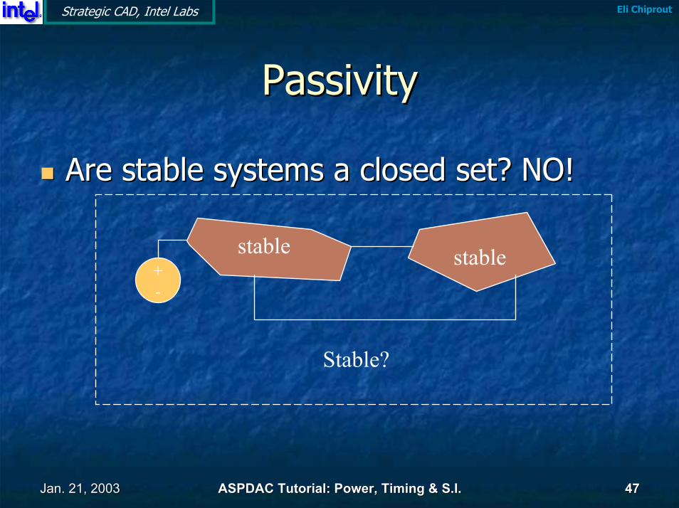
PassivityPassivity
Are stable systems a closed set? NO!Are stable systems a closed set? NO!
+-
stable stable
Stable?
Jan. 21, 2003Jan. 21, 2003 ASPDAC Tutorial: Power, Timing & S.I.ASPDAC Tutorial: Power, Timing & S.I. 4848
Eli ChiproutStrategic CAD, Intel Labs
References and further studyReferences and further study
M. M. CelikCelik, L. , L. PileggiPileggi, et al.,, et al.,“IC Interconnect Analysis”, “IC Interconnect Analysis”, KluwerKluwer academic, 2002academic, 2002“”Inductance 101: analysis and design issues”, K. Gala, D. “”Inductance 101: analysis and design issues”, K. Gala, D. BlaauwBlaauw, J. Wang, V. , J. Wang, V. ZolotovZolotov and M. Zhao, DAC, June 2001and M. Zhao, DAC, June 2001M. W. Beattie and L.T. M. W. Beattie and L.T. PileggiPileggi, “Inductance 101: Modeling and extraction”, DAC, June , “Inductance 101: Modeling and extraction”, DAC, June 20012001A. E. A. E. RuehliRuehli, “Inductance calculation in a complex integrated , “Inductance calculation in a complex integrated curcuitcurcuit environment”, environment”, IBM Journal of Research and Development, pages 470IBM Journal of Research and Development, pages 470--481, Sept. 1972.481, Sept. 1972.J. Rubinstein, P. Penfield and M.A. Horowitz, ``Signal Delay in J. Rubinstein, P. Penfield and M.A. Horowitz, ``Signal Delay in RCRC Tree Networks,'' Tree Networks,'' IEEE Trans. Computer-Aided Design, vol. CAD. CAD--2, No. 3, pp. 2022, No. 3, pp. 202--210, July 1983. 210, July 1983. C. J. Alpert, A. C. J. Alpert, A. DevganDevgan, and C. V. , and C. V. KashyapKashyap, “RC delay metric for performance , “RC delay metric for performance optimization”, IEEE Trans. on CAD, 20(5):571optimization”, IEEE Trans. on CAD, 20(5):571--582, May 2001582, May 2001W. C. Elmore, “the transient response of damped linear network wW. C. Elmore, “the transient response of damped linear network with particular ith particular regard to wideband amplifiers.” J. Applied Physics, p. 55regard to wideband amplifiers.” J. Applied Physics, p. 55--63, 1948.63, 1948.A. A. DevganDevgan, “Efficient coupled noise estimation for on, “Efficient coupled noise estimation for on--chip interconnects”, ICCAD chip interconnects”, ICCAD 1997, p. 1471997, p. 147--151.151.