Embed Size (px)
Citation preview
Assessing Chip-Level Impact of Double Patterning Lithography
Kwangok Jeong*, Andrew B. Kahng*,**, and Rasit O. Topaloglu***
http://vlsicad.ucsd.edu/
* ECE Dept., UC San Diego** CSE Dept., UC San Diego
*** GlobalFoundries, Inc.
(2)UCSD VLSI CAD Laboratory / GLOBALFOUNDRIES, Inc. - ISQED 2010, March 23, 2010
Outline
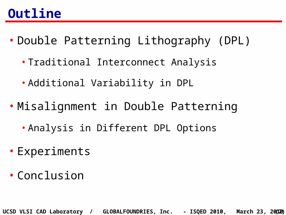
• Double Patterning Lithography (DPL)
• Traditional Interconnect Analysis
• Additional Variability in DPL
• Misalignment in Double Patterning
• Analysis in Different DPL Options
• Experiments
• Conclusion
(3)UCSD VLSI CAD Laboratory / GLOBALFOUNDRIES, Inc. - ISQED 2010, March 23, 2010
Outline
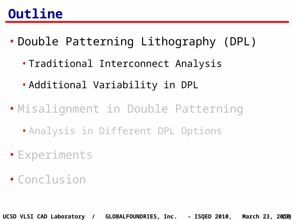
• Double Patterning Lithography (DPL)
• Traditional Interconnect Analysis
• Additional Variability in DPL
• Misalignment in Double Patterning
• Analysis in Different DPL Options
• Experiments
• Conclusion
(4)UCSD VLSI CAD Laboratory / GLOBALFOUNDRIES, Inc. - ISQED 2010, March 23, 2010
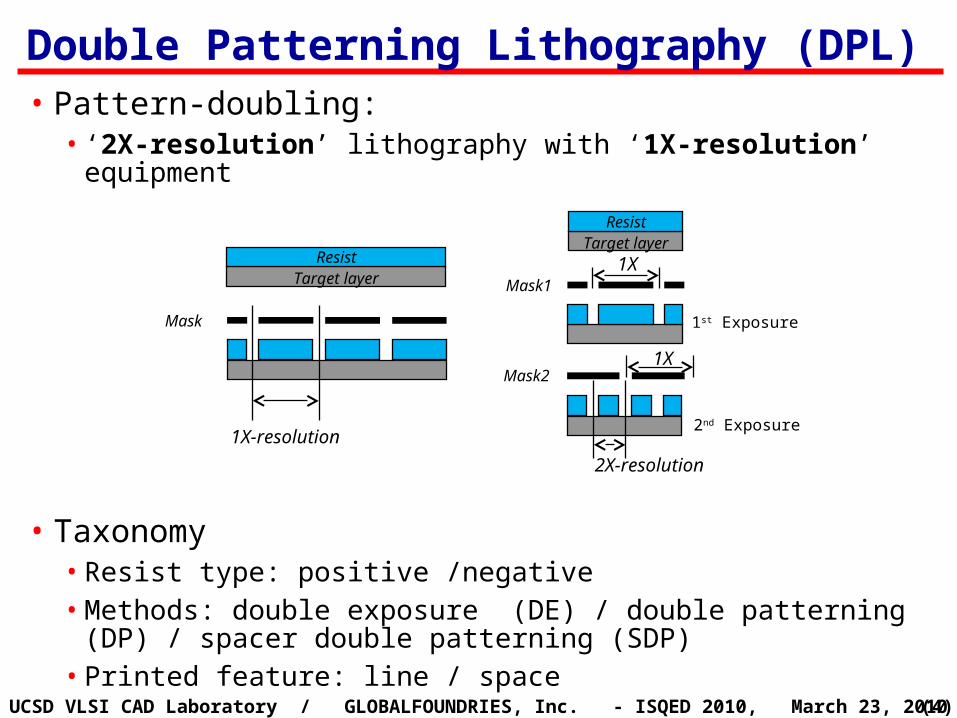
Double Patterning Lithography (DPL)• Pattern-doubling:
• ‘2X-resolution’ lithography with ‘1X-resolution’ equipment
• Taxonomy• Resist type: positive /negative• Methods: double exposure (DE) / double patterning (DP) /
spacer double patterning (SDP)• Printed feature: line / space
Target layerResist
1st Exposure
2nd Exposure
Mask1
Mask2
Target layerResist
Mask
1X-resolution
1X
2X-resolution
1X
(5)UCSD VLSI CAD Laboratory / GLOBALFOUNDRIES, Inc. - ISQED 2010, March 23, 2010
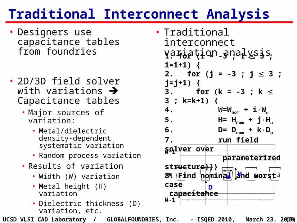
Traditional Interconnect Analysis• Designers use capacitance
tables from foundries
• 2D/3D field solver with variations Capacitance tables • Major sources of variation:
• Metal/dielectric density-dependent systematic variation
• Random process variation
• Results of variation• Width (W) variation• Metal height (H) variation• Dielectric thickness (D)
variation, etc.
• Traditional interconnect variation analysis1. for (i = -3 ; i 3 ; i=i+1) {2. for (j = -3 ; j 3 ; j=j+1) {3. for (k = -3 ; k 3 ; k=k+1) {4. W=Wnom + iW
5. H= Hnom + jH
6. D= Dnom + kD
7. run field solver over parameterized structure}}}8. Find nominal and worst-case capacitance
M+1
M-1
M W H
D
(6)UCSD VLSI CAD Laboratory / GLOBALFOUNDRIES, Inc. - ISQED 2010, March 23, 2010
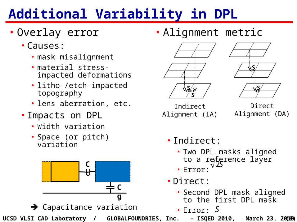
Additional Variability in DPL• Overlay error
• Causes: • mask misalignment • material stress-impacted
deformations• litho-/etch-impacted
topography• lens aberration, etc.
• Impacts on DPL• Width variation• Space (or pitch) variation
Capacitance variation
• Alignment metric
• Indirect: • Two DPL masks aligned to
a reference layer• Error:
• Direct: • Second DPL mask aligned
to the first DPL mask• Error:
SS
S
S
IndirectAlignment (IA)
Cc
Cg
DirectAlignment (DA)
S2
S
(7)UCSD VLSI CAD Laboratory / GLOBALFOUNDRIES, Inc. - ISQED 2010, March 23, 2010
Outline
• Double Patterning Lithography (DPL)
• Traditional Interconnect Analysis
• Additional Variability in DPL
• Misalignment in Double Patterning
• Analysis in Different DPL Options
• Experiments
• Conclusion
(8)UCSD VLSI CAD Laboratory / GLOBALFOUNDRIES, Inc. - ISQED 2010, March 23, 2010
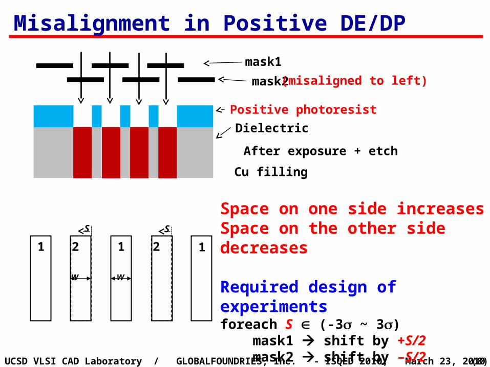
Misalignment in Positive DE/DP
1 2 1 2 1
W W
S S
mask2
Positive photoresist
Dielectric
Space on one side increasesSpace on the other side decreases
Required design of experiments foreach S (-3 ~ 3) mask1 shift by +S/2 mask2 shift by –S/2end
mask1
After exposure + etch
Cu filling
(misaligned to left)
(9)UCSD VLSI CAD Laboratory / GLOBALFOUNDRIES, Inc. - ISQED 2010, March 23, 2010
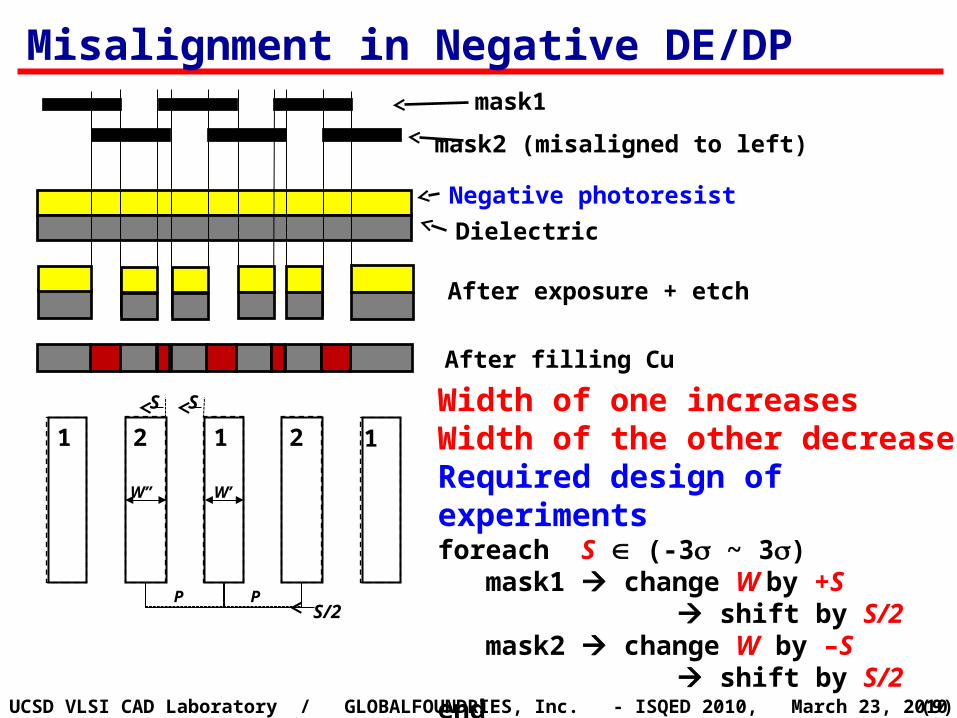
Misalignment in Negative DE/DP
1 2 1 2 1
W’’ W’
S S
P PS/2
mask1
mask2 (misaligned to left)
Negative photoresist
Dielectric
After exposure + etch
After filling Cu
Width of one increasesWidth of the other decreasesRequired design of experiments foreach S (-3 ~ 3) mask1 change W by +S shift by S/2 mask2 change W by –S shift by S/2end
(10)UCSD VLSI CAD Laboratory / GLOBALFOUNDRIES, Inc. - ISQED 2010, March 23, 2010
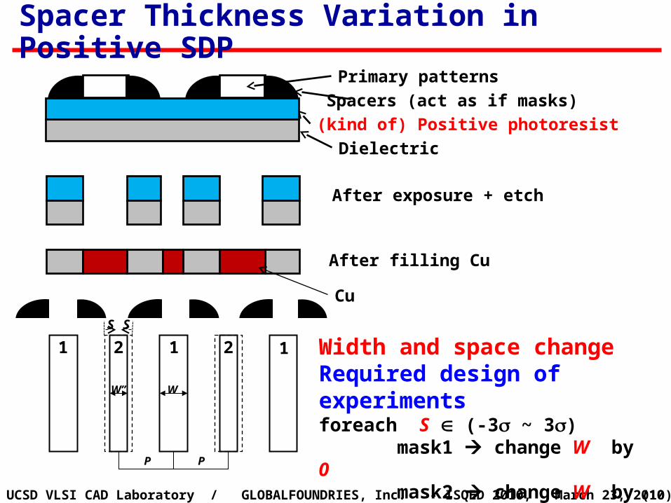
Spacer Thickness Variation in Positive SDP
Dielectric
After exposure + etch
(kind of) Positive photoresist
Primary patterns
Spacers (act as if masks)
After filling Cu
Cu
Width and space changeRequired design of experiments foreach S (-3 ~ 3) mask1 change W by 0 mask2 change W by +Send
1 2 1 2 1
WW’’
P P
S S
(11)UCSD VLSI CAD Laboratory / GLOBALFOUNDRIES, Inc. - ISQED 2010, March 23, 2010
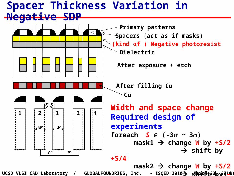
Spacer Thickness Variation in Negative SDP
1 2 1 2 1
W’ W’
P’’ P’
S S
Primary patterns
Dielectric
After exposure + etch
After filling Cu
Spacers (act as if masks)
(kind of ) Negative photoresist
Cu
Width and space changeRequired design of experiments foreach S (-3 ~ 3) mask1 change W by +S/2 shift by +S/4 mask2 change W by +S/2 shift by –S/4end
(12)UCSD VLSI CAD Laboratory / GLOBALFOUNDRIES, Inc. - ISQED 2010, March 23, 2010
Outline
• Double Patterning Lithography (DPL)
• Traditional Interconnect Analysis
• Misalignment in Double Patterning
• Analysis in Different DPL Options
• Experiments
• Conclusion
(13)UCSD VLSI CAD Laboratory / GLOBALFOUNDRIES, Inc. - ISQED 2010, March 23, 2010
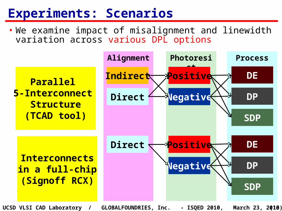
Photoresist ProcessAlignment
Experiments: Scenarios• We examine impact of misalignment and linewidth
variation across various DPL options
Parallel 5-Interconnect
Structure(TCAD tool)
Interconnectsin a full-chip
(Signoff RCX)
Indirect
Direct
Positive
Negative
DE
DP
SDP
Direct Positive
Negative
DE
DP
SDP
(14)UCSD VLSI CAD Laboratory / GLOBALFOUNDRIES, Inc. - ISQED 2010, March 23, 2010
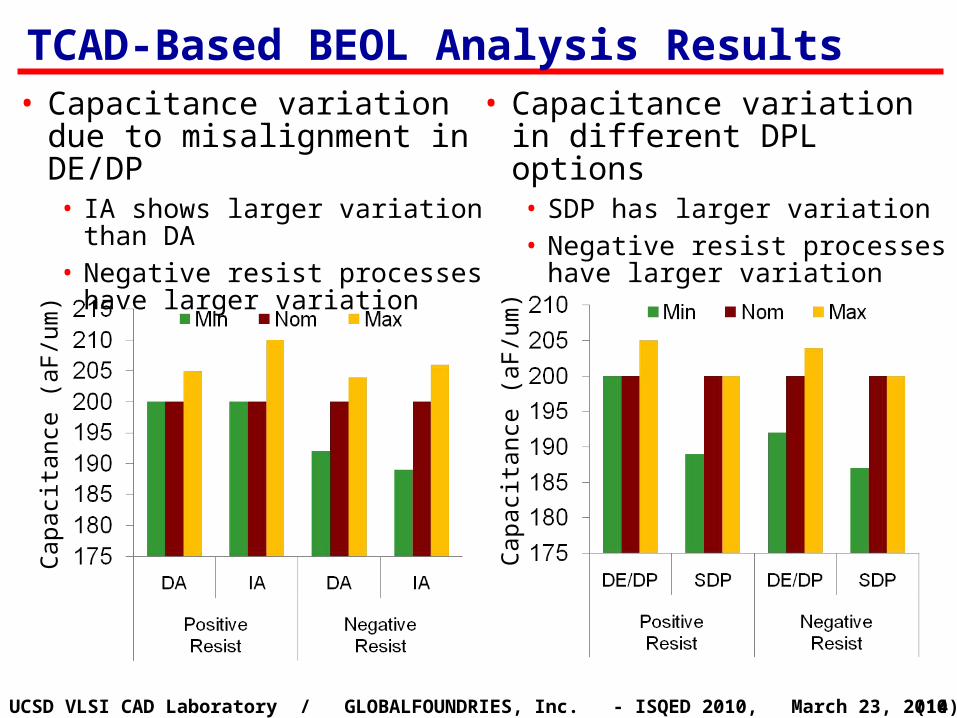
TCAD-Based BEOL Analysis Results• Capacitance variation due to
misalignment in DE/DP• IA shows larger variation than DA• Negative resist processes have
larger variation
• Capacitance variation in different DPL options• SDP has larger variation• Negative resist processes have
larger variation
Cap
acita
nce
(aF
/um
)
Cap
acita
nce
(aF
/um
)
(15)UCSD VLSI CAD Laboratory / GLOBALFOUNDRIES, Inc. - ISQED 2010, March 23, 2010
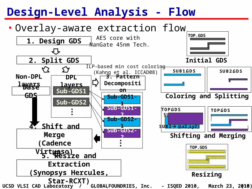
Design-Level Analysis - Flow• Overlay-aware extraction flow
1. Design GDSTOP.GDS
Initial GDS
AES core with NanGate 45nm Tech.
2. Split GDS
Base GDS Sub-GDS1
Sub-GDS2
DPL layersNon-DPL layers 3. PatternDecomposition
Sub-GDS1-1
Sub-GDS1-2
Sub-GDS2-1
Sub-GDS2-2
ILP-based min cost coloring(Kahng et al. ICCAD08)
Coloring and Splitting
SUB2.GDSSUB1.GDS
4. Shift and Merge(Cadence Virtuoso)
Shifting and Merging
SUB1 (x1, y1)TOP.GDS
SUB2 (x2, y2)
TOP.GDS
TOP.GDS
5. Resize and Extraction(Synopsys Hercules, Star-RCXT) Resizing
(16)UCSD VLSI CAD Laboratory / GLOBALFOUNDRIES, Inc. - ISQED 2010, March 23, 2010
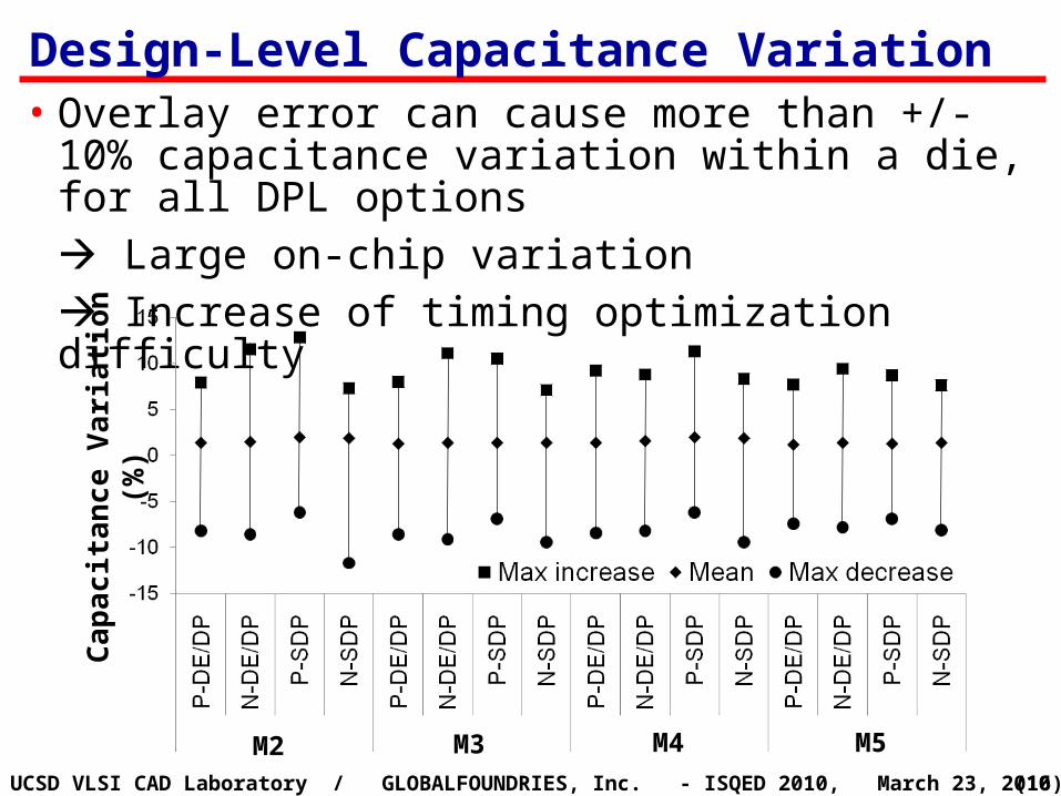
• Overlay error can cause more than +/- 10% capacitance variation within a die, for all DPL options
Large on-chip variation Increase of timing optimization difficulty
Ca
pac
ita
nc
e V
ari
ati
on
(%
)
Design-Level Capacitance Variation
M2 M3 M4 M5

(17)UCSD VLSI CAD Laboratory / GLOBALFOUNDRIES, Inc. - ISQED 2010, March 23, 2010
• A net having maximum crosstalk delay (17um long)• SDP shows more sensitivity tighten overlay spec• P-DE/DP shows least sensitivity lessen overlay spec
Maximum Crosstalk-Induced Delay
P-DE/DP(Space on one side)
N-DE/DP(Width)
P-SDP(Spaces on both sides)
N-SDP(Space & width)
M4
|S| |S|/2 |S|/2 |S|/2
M2 M4 M2 M4
w/o metal fill w/ metal fill
(18)UCSD VLSI CAD Laboratory / GLOBALFOUNDRIES, Inc. - ISQED 2010, March 23, 2010
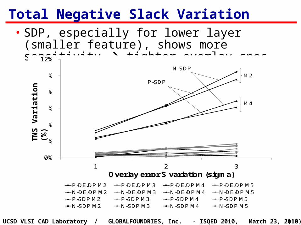
Total Negative Slack Variation• SDP, especially for lower layer (smaller feature),
shows more sensitivity tighter overlay spec
0%
2%
4%
6%
8%
10%
12%
1 2 3
TN
S V
ari
ati
on
(%
)
Overlay error S variation (sigma)
P-DE/DP M2 P-DE/DP M3 P-DE/DP M4 P-DE/DP M5N-DE/DP M2 N-DE/DP M3 N-DE/DP M4 N-DE/DP M5P-SDP M2 P-SDP M3 P-SDP M4 P-SDP M5N-SDP M2 N-SDP M3 N-SDP M4 N-SDP M5
P-SDP
N-SDPM2
M4
TN
S V
aria
tio
n (
%)
(19)UCSD VLSI CAD Laboratory / GLOBALFOUNDRIES, Inc. - ISQED 2010, March 23, 2010
Outline
• Double Patterning Lithography (DPL)
• Traditional Interconnect Analysis
• Misalignment in Double Patterning
• Analysis in Different DPL Options
• Experiments
• Conclusion
(20)UCSD VLSI CAD Laboratory / GLOBALFOUNDRIES, Inc. - ISQED 2010, March 23, 2010
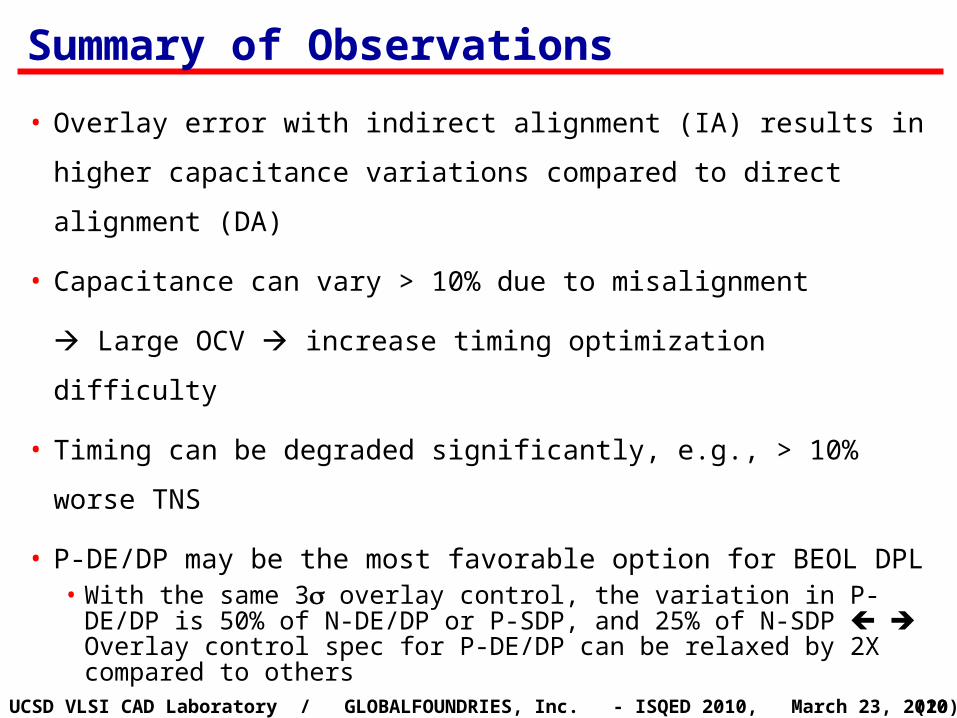
Summary of Observations
• Overlay error with indirect alignment (IA) results in higher
capacitance variations compared to direct alignment (DA)
• Capacitance can vary > 10% due to misalignment
Large OCV increase timing optimization difficulty
• Timing can be degraded significantly, e.g., > 10% worse TNS
• P-DE/DP may be the most favorable option for BEOL DPL • With the same 3 overlay control, the variation in P-DE/DP is
50% of N-DE/DP or P-SDP, and 25% of N-SDP Overlay control spec for P-DE/DP can be relaxed by 2X compared to others
(21)UCSD VLSI CAD Laboratory / GLOBALFOUNDRIES, Inc. - ISQED 2010, March 23, 2010
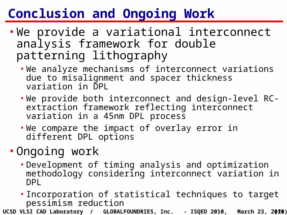
Conclusion and Ongoing Work
• We provide a variational interconnect analysis framework for double patterning lithography• We analyze mechanisms of interconnect variations due to
misalignment and spacer thickness variation in DPL• We provide both interconnect and design-level RC-
extraction framework reflecting interconnect variation in a 45nm DPL process
• We compare the impact of overlay error in different DPL options
• Ongoing work• Development of timing analysis and optimization
methodology considering interconnect variation in DPL• Incorporation of statistical techniques to target pessimism
reduction

Thank You!
(23)UCSD VLSI CAD Laboratory / GLOBALFOUNDRIES, Inc. - ISQED 2010, March 23, 2010
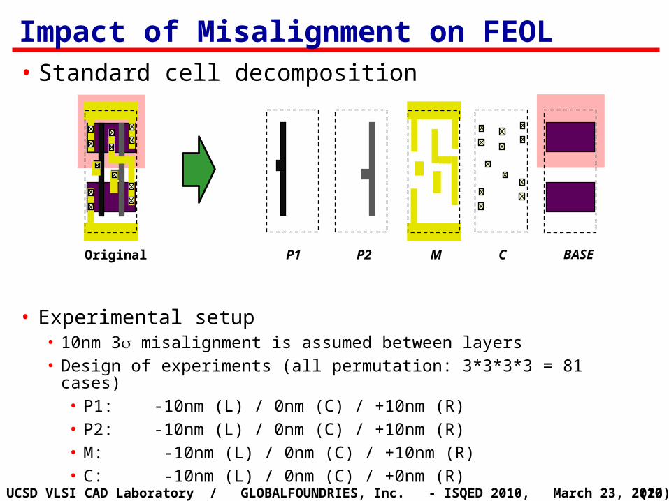
Impact of Misalignment on FEOL• Standard cell decomposition
• Experimental setup• 10nm 3 misalignment is assumed between layers• Design of experiments (all permutation: 3*3*3*3 = 81 cases)
• P1: -10nm (L) / 0nm (C) / +10nm (R)• P2: -10nm (L) / 0nm (C) / +10nm (R)• M: -10nm (L) / 0nm (C) / +10nm (R)• C: -10nm (L) / 0nm (C) / +0nm (R)
Original MP1 P2 C BASE
(24)UCSD VLSI CAD Laboratory / GLOBALFOUNDRIES, Inc. - ISQED 2010, March 23, 2010
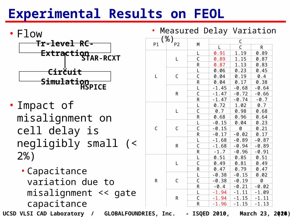
Experimental Results on FEOL
• Flow
• Impact of misalignment on cell delay is negligibly small (< 2%)• Capacitance variation due
to misalignment << gate capacitance
• Measured Delay Variation (%)
P1 P2 MC
L C R
L
LL 0.91 1.19 0.89C 0.89 1.15 0.87R 0.87 1.13 0.83
CL 0.06 0.23 0.45C 0.04 0.19 0.4R 0.04 0.17 0.38
RL -1.45 -0.68 -0.64C -1.47 -0.72 -0.66R -1.47 -0.74 -0.7
C
LL 0.72 1.02 0.7C 0.7 0.98 0.68R 0.68 0.96 0.64
CL -0.15 0.04 0.23C -0.15 0 0.21R -0.17 -0.02 0.17
RL -1.68 -0.89 -0.87C -1.68 -0.94 -0.89R -1.7 -0.96 -0.91
R
LL 0.51 0.85 0.51C 0.49 0.81 0.49R 0.47 0.79 0.47
CL -0.38 -0.15 0.02C -0.38 -0.19 0R -0.4 -0.21 -0.02
RL -1.94 -1.11 -1.09C -1.94 -1.15 -1.11R -1.96 -1.15 -1.13
Tr-level RC-ExtractionSTAR-RCXT
Circuit SimulationHSPICE
(25)UCSD VLSI CAD Laboratory / GLOBALFOUNDRIES, Inc. - ISQED 2010, March 23, 2010
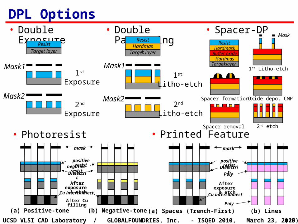
DPL Options• Double Exposure • Double Patterning • Spacer-DP
• Photoresist • Printed Featuremask
positive resistnegative resist
After exposure & etch
Dielectric
After Cu filling
(a) Positive-tone (b) Negative-tone
Cu interconnect
mask
positive resist
After exposure & etch
Dielectric
(a) Spaces (Trench-First) (b) Lines
Cu interconnect
Poly
Poly
Target layer
ResistHardmask
Buffer oxideHardmask
Target layer1st Litho-etch
Spacer formation Oxide depo. CMP
Spacer removal 2nd etch
Mask
Target layer
ResistHardmask
1st Litho-etch
2nd Litho-etch
Mask1
Mask2
Target layer
Resist
1st Exposure
2nd Exposure
Mask1
Mask2
(26)UCSD VLSI CAD Laboratory / GLOBALFOUNDRIES, Inc. - ISQED 2010, March 23, 2010
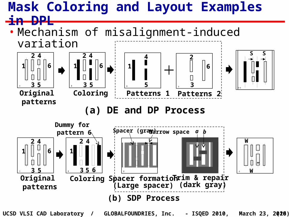
Mask Coloring and Layout Examples in DPL• Mechanism of misalignment-induced variation
(a) DE and DP Process
(b) SDP Process
1
2
3
4
5
6 1
2
3
4
5
6 1
4
5
2
3
6
Original patterns
Original patterns
Coloring Patterns 1 Patterns 2
Coloring Spacer formation(Large spacer)
Trim & repair (dark gray)
S S
Narrow space
W
1
2
3
4
5
6
W”
Dummy for pattern 6
1
4
5
2
3 6
Spacer (gray) a b
(27)UCSD VLSI CAD Laboratory / GLOBALFOUNDRIES, Inc. - ISQED 2010, March 23, 2010
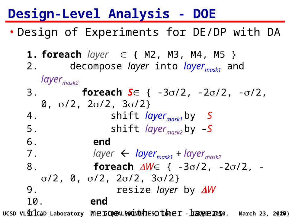
Design-Level Analysis - DOE• Design of Experiments for DE/DP with DA
1. foreach layer { M2, M3, M4, M5 }2. decompose layer into layermask1 and layermask2
3. foreach S { -3/2, -2/2, -/2, 0, /2, 2/2, 3/2} 4. shift layermask1 by S5. shift layermask2 by –S6. end7. layer layermask1 + layermask2
8. foreach W { -3/2, -2/2, -/2, 0, /2, 2/2, 3/2}9. resize layer by W 10. end11. merge with other layers12. RC-Extraction and Timing Analysis13. end
(28)UCSD VLSI CAD Laboratory / GLOBALFOUNDRIES, Inc. - ISQED 2010, March 23, 2010
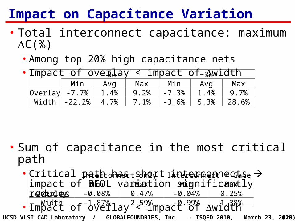
Impact on Capacitance Variation• Total interconnect capacitance: maximum C(%)
• Among top 20% high capacitance nets• Impact of overlay < impact of width
• Sum of capacitance in the most critical path• Critical path has short interconnects impact of BEOL
variation significantly reduces• Impact of overlay < impact of width
-3 +3Min Avg Max Min Avg Max
Overlay -7.7% 1.4% 9.2% -7.3% 1.4% 9.7%Width -22.2% 4.7% 7.1% -3.6% 5.3% 28.6%
Interconnect only Interconnect + GateMin Max Min Max
Overlay -0.08% 0.47% -0.04% 0.25%Width -1.87% 2.59% -0.99% 1.38%
(29)UCSD VLSI CAD Laboratory / GLOBALFOUNDRIES, Inc. - ISQED 2010, March 23, 2010
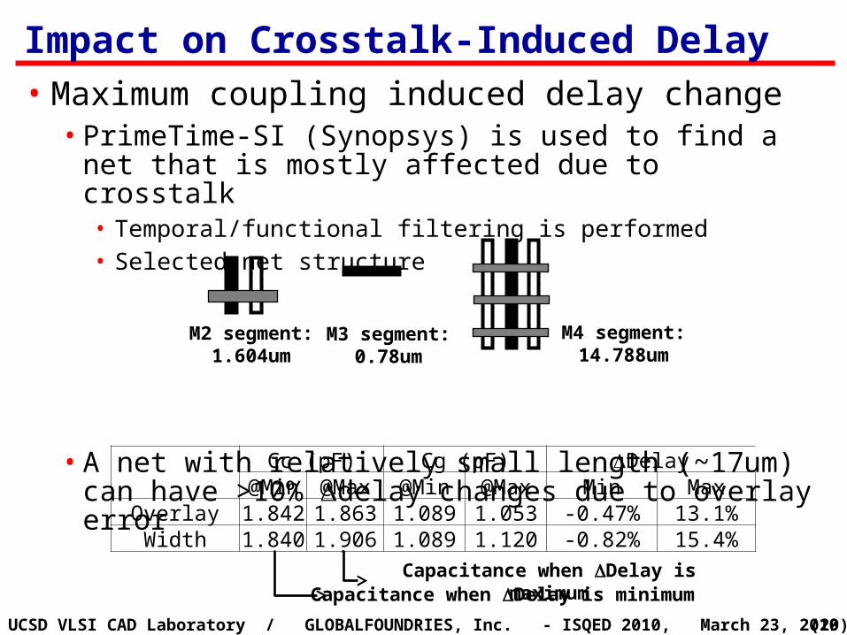
Impact on Crosstalk-Induced Delay• Maximum coupling induced delay change
• PrimeTime-SI (Synopsys) is used to find a net that is mostly affected due to crosstalk• Temporal/functional filtering is performed• Selected net structure
• A net with relatively small length (~17um) can have >10% delay changes due to overlay error
Cc (pF) Cg (pF) Delay@Min @Max @Min @Max Min Max
Overlay 1.842 1.863 1.089 1.053 -0.47% 13.1%Width 1.840 1.906 1.089 1.120 -0.82% 15.4%
M2 segment:1.604um
M3 segment:0.78um
M4 segment:14.788um
Capacitance when Delay is minimumCapacitance when Delay is maximum
(30)UCSD VLSI CAD Laboratory / GLOBALFOUNDRIES, Inc. - ISQED 2010, March 23, 2010
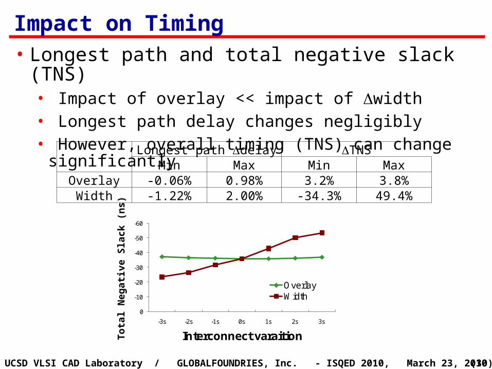
Impact on Timing• Longest path and total negative slack (TNS)
• Impact of overlay << impact of width• Longest path delay changes negligibly• However, overall timing (TNS) can change significantly
Longest path delay TNSMin Max Min Max
Overlay -0.06% 0.98% 3.2% 3.8%Width -1.22% 2.00% -34.3% 49.4%
To
tal
Ne
gat
ive
Sla
ck (
ns)
-60
-50
-40
-30
-20
-10
0
-3s -2s -1s 0s 1s 2s 3s
Interconnect varaition
OverlayWidth