Embed Size (px)
Citation preview
AT30TS75A
9- to 12-bit Selectable, ±0.5°C Accurate
Digital Temperature Sensor
DATASHEET
See Errata in Section 12.
Features
Single 1.7V to 5.5V Supply
Measures Temperature from -55C to +125C
Highly Accurate Temperature Measurements Requiring No External Components
±0.5C Accuracy (Typical) Over the 0C to +85C Range
±1.0C Accuracy (Typical) Over the -25C to +105C Range
±2.0C Accuracy (Typical) Over the -40C to +125C Range
User-configurable Resolution
9 to 12 bits (0.5C to 0.0625C)
User-configurable High and Low Temperature Limits
ALERT Output Pin for Indicating Temperature Alarms
2-wire I2C and SMBus™ Compatible Serial Interface
Supports SMBus Timeout
Supports SMBus Alert and Alert Response Address (ARA)
Selectable Addressing Allows up to Eight Devices on the Same Bus
I2C High-Speed (HS) Mode Compatible
3.4MHz Maximum Clock Frequency
Built-in Noise Suppression Filtering for Clock and Data Input Signals
Low Power Dissipation
85μA Active Current (Typical) During Temperature Measurements
Shutdown Mode to Minimize Power Consumption
1μA Shutdown Current (Typical)
One-Shot Mode for Single Temperature Measurement While in Shutdown Mode
Pin and Software Compatible to Industry-standard LM75-type Devices
Industry Standard Green (Pb/Halide-free/RoHS Compliant) Package Options
8-lead SOIC (150-mil)
8-lead MSOP (3 x 3mm)
8-pad Ultra Thin DFN (UDFN — 2.0 x 3.0 x 0.6mm)
Atmel-8839I-DTS-AT30TS75A-Datasheet_102014
Table of Contents
1. Description . . . . . . . . . . . . . . . . . . . . . . . . . . . . . . . . . . . . . . . . . . . . . . . . . . . . . . . 4
2. Pin Descriptions and Pinouts . . . . . . . . . . . . . . . . . . . . . . . . . . . . . . . . . . . . . . 5
3. Block Diagram . . . . . . . . . . . . . . . . . . . . . . . . . . . . . . . . . . . . . . . . . . . . . . . . . . . . 6
4. Device Communication . . . . . . . . . . . . . . . . . . . . . . . . . . . . . . . . . . . . . . . . . . . . 74.1 Start Condition . . . . . . . . . . . . . . . . . . . . . . . . . . . . . . . . . . . . . . . . . . . . . . . . . 7
4.2 Stop Condition. . . . . . . . . . . . . . . . . . . . . . . . . . . . . . . . . . . . . . . . . . . . . . . . . . 7
4.3 Acknowledge (ACK) . . . . . . . . . . . . . . . . . . . . . . . . . . . . . . . . . . . . . . . . . . . . . 7
4.4 No-Acknowledge (NACK) . . . . . . . . . . . . . . . . . . . . . . . . . . . . . . . . . . . . . . . . . 8
5. Device Operation . . . . . . . . . . . . . . . . . . . . . . . . . . . . . . . . . . . . . . . . . . . . . . . . . 95.1 High-Speed Mode . . . . . . . . . . . . . . . . . . . . . . . . . . . . . . . . . . . . . . . . . . . . . . . 9
5.2 Temperature Measurements. . . . . . . . . . . . . . . . . . . . . . . . . . . . . . . . . . . . . . 10
5.3 Temperature Alarm . . . . . . . . . . . . . . . . . . . . . . . . . . . . . . . . . . . . . . . . . . . . . 10
5.3.1 Fault Tolerance Limits . . . . . . . . . . . . . . . . . . . . . . . . . . . . . . . . . . . 10
5.3.2 Comparator Mode . . . . . . . . . . . . . . . . . . . . . . . . . . . . . . . . . . . . . . 11
5.3.3 Interrupt Mode . . . . . . . . . . . . . . . . . . . . . . . . . . . . . . . . . . . . . . . . . 12
5.4 Shutdown Mode . . . . . . . . . . . . . . . . . . . . . . . . . . . . . . . . . . . . . . . . . . . . . . . 13
5.4.1 One-Shot Mode . . . . . . . . . . . . . . . . . . . . . . . . . . . . . . . . . . . . . . . . 13
6. Registers . . . . . . . . . . . . . . . . . . . . . . . . . . . . . . . . . . . . . . . . . . . . . . . . . . . . . . . . 14
6.1 Pointer Register . . . . . . . . . . . . . . . . . . . . . . . . . . . . . . . . . . . . . . . . . . . . . . . 14
6.2 Temperature Register . . . . . . . . . . . . . . . . . . . . . . . . . . . . . . . . . . . . . . . . . . . 16
6.3 Configuration Register . . . . . . . . . . . . . . . . . . . . . . . . . . . . . . . . . . . . . . . . . . 18
6.3.1 OS Bit . . . . . . . . . . . . . . . . . . . . . . . . . . . . . . . . . . . . . . . . . . . . . . . 19
6.3.2 R1:R0 Bits . . . . . . . . . . . . . . . . . . . . . . . . . . . . . . . . . . . . . . . . . . . . 19
6.3.3 FT1:FT0 Bits . . . . . . . . . . . . . . . . . . . . . . . . . . . . . . . . . . . . . . . . . . 19
6.3.4 POL Bit . . . . . . . . . . . . . . . . . . . . . . . . . . . . . . . . . . . . . . . . . . . . . . 19
6.3.5 CMP/INT Bit . . . . . . . . . . . . . . . . . . . . . . . . . . . . . . . . . . . . . . . . . . . 20
6.3.6 SD Bit . . . . . . . . . . . . . . . . . . . . . . . . . . . . . . . . . . . . . . . . . . . . . . . . 20
6.4 TLOW and THIGH Limit Registers . . . . . . . . . . . . . . . . . . . . . . . . . . . . . . . . . . . . 21
7. SMBus Features and I2C General Call . . . . . . . . . . . . . . . . . . . . . . . . . . . . 23
7.1 SMBus Alert . . . . . . . . . . . . . . . . . . . . . . . . . . . . . . . . . . . . . . . . . . . . . . . . . . 23
7.2 SMBus Timeout. . . . . . . . . . . . . . . . . . . . . . . . . . . . . . . . . . . . . . . . . . . . . . . . 24
7.3 General Call . . . . . . . . . . . . . . . . . . . . . . . . . . . . . . . . . . . . . . . . . . . . . . . . . . 24
8. Electrical Specifications . . . . . . . . . . . . . . . . . . . . . . . . . . . . . . . . . . . . . . . . . . 25
8.1 Absolute Maximum Ratings . . . . . . . . . . . . . . . . . . . . . . . . . . . . . . . . . . . . . . 25
8.2 DC and AC Operating Range . . . . . . . . . . . . . . . . . . . . . . . . . . . . . . . . . . . . . 25
8.3 DC Characteristics . . . . . . . . . . . . . . . . . . . . . . . . . . . . . . . . . . . . . . . . . . . . . 26
8.4 Temperature Sensor Accuracy and Conversion Characteristics . . . . . . . . . . 27
8.5 AC Characteristics . . . . . . . . . . . . . . . . . . . . . . . . . . . . . . . . . . . . . . . . . . . . . 27
8.6 Power-Up Conditions . . . . . . . . . . . . . . . . . . . . . . . . . . . . . . . . . . . . . . . . . . . 28
8.7 Pin Capacitance . . . . . . . . . . . . . . . . . . . . . . . . . . . . . . . . . . . . . . . . . . . . . . . 29
8.8 Input Test Waveforms and Measurement Levels . . . . . . . . . . . . . . . . . . . . . . 29
8.9 Output Test Load . . . . . . . . . . . . . . . . . . . . . . . . . . . . . . . . . . . . . . . . . . . . . . 29
AT30TS75A [DATASHEET]Atmel-8839I-DTS-AT30TS75A-Datasheet_102014
2
9. Ordering Information . . . . . . . . . . . . . . . . . . . . . . . . . . . . . . . . . . . . . . . . . . . . . 30
9.1 Atmel Ordering Code Detail . . . . . . . . . . . . . . . . . . . . . . . . . . . . . . . . . . . . . . 30
9.2 Green Package Options (Pb/Halide-free/RoHS Compliant) . . . . . . . . . . . . . . 30
10. Part Marking Detail . . . . . . . . . . . . . . . . . . . . . . . . . . . . . . . . . . . . . . . . . . . . . . 31
11. Packaging Information . . . . . . . . . . . . . . . . . . . . . . . . . . . . . . . . . . . . . . . . . . . 32
11.1 8S1 — 8-lead JEDEC SOIC . . . . . . . . . . . . . . . . . . . . . . . . . . . . . . . . . . . . . . 32
11.2 8XM — 8-lead MSOP . . . . . . . . . . . . . . . . . . . . . . . . . . . . . . . . . . . . . . . . . . . 33
11.3 8MA2 — 8-pad UDFN. . . . . . . . . . . . . . . . . . . . . . . . . . . . . . . . . . . . . . . . . . . 34
12. Errata . . . . . . . . . . . . . . . . . . . . . . . . . . . . . . . . . . . . . . . . . . . . . . . . . . . . . . . . . . . 35
12.1 ALERT Pin State . . . . . . . . . . . . . . . . . . . . . . . . . . . . . . . . . . . . . . . . . . . . . . . 35
13. Revision History . . . . . . . . . . . . . . . . . . . . . . . . . . . . . . . . . . . . . . . . . . . . . . . . . 36
3AT30TS75A [DATASHEET]Atmel-8839I-DTS-AT30TS75A-Datasheet_102014
1. Description
The Atmel® AT30TS75A is a complete, precise temperature monitoring device designed for use in a variety of
applications that require the measuring of local temperatures as an integral part of the system's function and/or reliability.
The AT30TS75A device combines a high-precision digital temperature sensor, programmable high and low temperature
alarms, and a 2-wire I2C and SMBus (System Management Bus) compatible serial interface into a single, compact
package.
The temperature sensor can measure temperatures over the full -55C to +125C temperature range and has a typical
accuracy as precise as ±0.5C from 0C to +85C. The result of the digitized temperature measurements are stored in
one of the AT30TS75A internal registers, which is readable at any time through the device's serial interface.
The AT30TS75A utilizes flexible, user-programmable internal registers to configure the temperature sensor's
performance and response to high and low temperature conditions. A dedicated alarm output activates if the temperature
measurement exceeds the user-defined temperature and fault count limits. To reduce current consumption and save
power, the AT30TS75A features a Shutdown mode that turns off all internal circuitry except for the internal Power-On
Reset (POR) and serial interface circuits.
The AT30TS75A is factory-calibrated and requires no external components to measure temperature. With its flexibility
and high-degree of accuracy, the AT30TS75A is ideal for extended temperature measurements in a wide variety of
communication, computer, consumer, environmental, industrial, and instrumentation applications.
AT30TS75A [DATASHEET]Atmel-8839I-DTS-AT30TS75A-Datasheet_102014
4
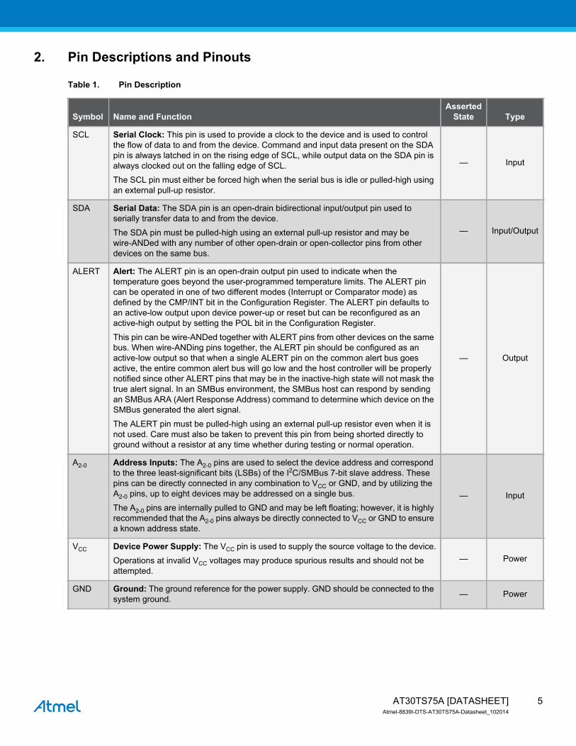
2. Pin Descriptions and Pinouts
Table 1. Pin Description
Symbol Name and Function
Asserted
State Type
SCL Serial Clock: This pin is used to provide a clock to the device and is used to control
the flow of data to and from the device. Command and input data present on the SDA
pin is always latched in on the rising edge of SCL, while output data on the SDA pin is
always clocked out on the falling edge of SCL.
The SCL pin must either be forced high when the serial bus is idle or pulled-high using
an external pull-up resistor.
— Input
SDA Serial Data: The SDA pin is an open-drain bidirectional input/output pin used to
serially transfer data to and from the device.
The SDA pin must be pulled-high using an external pull-up resistor and may be
wire-ANDed with any number of other open-drain or open-collector pins from other
devices on the same bus.
— Input/Output
ALERT Alert: The ALERT pin is an open-drain output pin used to indicate when the
temperature goes beyond the user-programmed temperature limits. The ALERT pin
can be operated in one of two different modes (Interrupt or Comparator mode) as
defined by the CMP/INT bit in the Configuration Register. The ALERT pin defaults to
an active-low output upon device power-up or reset but can be reconfigured as an
active-high output by setting the POL bit in the Configuration Register.
This pin can be wire-ANDed together with ALERT pins from other devices on the same
bus. When wire-ANDing pins together, the ALERT pin should be configured as an
active-low output so that when a single ALERT pin on the common alert bus goes
active, the entire common alert bus will go low and the host controller will be properly
notified since other ALERT pins that may be in the inactive-high state will not mask the
true alert signal. In an SMBus environment, the SMBus host can respond by sending
an SMBus ARA (Alert Response Address) command to determine which device on the
SMBus generated the alert signal.
The ALERT pin must be pulled-high using an external pull-up resistor even when it is
not used. Care must also be taken to prevent this pin from being shorted directly to
ground without a resistor at any time whether during testing or normal operation.
— Output
A2-0 Address Inputs: The A2-0 pins are used to select the device address and correspond
to the three least-significant bits (LSBs) of the I2C/SMBus 7-bit slave address. These
pins can be directly connected in any combination to VCC or GND, and by utilizing the
A2-0 pins, up to eight devices may be addressed on a single bus.
The A2-0 pins are internally pulled to GND and may be left floating; however, it is highly
recommended that the A2-0 pins always be directly connected to VCC or GND to ensure
a known address state.
— Input
VCC Device Power Supply: The VCC pin is used to supply the source voltage to the device.
Operations at invalid VCC voltages may produce spurious results and should not be
attempted.
— Power
GND Ground: The ground reference for the power supply. GND should be connected to the
system ground.— Power
5AT30TS75A [DATASHEET]Atmel-8839I-DTS-AT30TS75A-Datasheet_102014
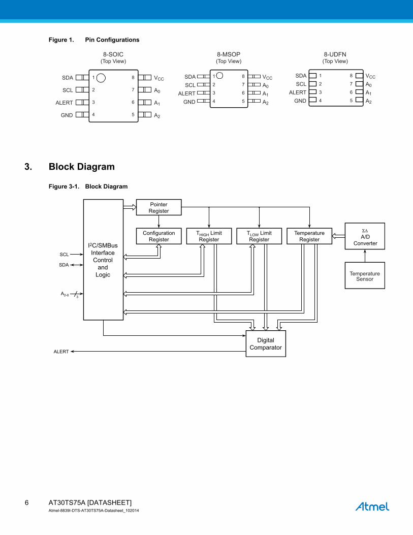
Figure 1. Pin Configurations
3. Block Diagram
Figure 3-1. Block Diagram
8-SOIC(Top View)
8-MSOP(Top View)
8-UDFN(Top View)
SDA
SCL
ALERT
GND
VCC
A0
A1
A2
SDASCL
ALERTGND
SDASCL
ALERTGND
VCC
A0
A1
A2
VCC
A0
A1
A2
1
2
3
4
8
7
6
5
1
2
3
4
8
7
6
5
1
2
3
4
8
7
6
5
I2C/SMBusInterfaceControl
andLogic
DigitalComparator
PointerRegister
ConfigurationRegister
THIGH LimitRegister
TLOW LimitRegister
TemperatureRegister A/D
Converter
TemperatureSensor
SCL
SDA
A2-0
ALERT
3
AT30TS75A [DATASHEET]Atmel-8839I-DTS-AT30TS75A-Datasheet_102014
6
4. Device Communication
The AT30TS75A operates as a slave device and utilizes a simple 2-wire I2C and SMBus compatible digital serial
interface to communicate with a host controller, commonly referred to as the bus Master. The Master initiates and
controls all Read and Write operations to the slave devices on the serial bus, and both the Master and the slave devices
can transmit and receive data on the bus.
The serial interface is comprised of just two signal lines: Serial Clock (SCL) and Serial Data (SDA). The SCL pin is used
to receive the clock signal from the Master, while the bidirectional SDA pin is used to receive command and data
information from the Master as well as to send data back to the Master. Data is always latched into the AT30TS75A on
the rising edge of SCL and always output from the device on the falling edge of SCL. Both the SCL and SDA pin
incorporate integrated spike suppression filters and Schmitt Triggers to minimize the effects of input spikes and bus
noise.
All command and data information is transferred with the Most-Significant Bit (MSB) first. During bus communication, one
data bit is transmitted every clock cycle, and after eight bits (one byte) of data has been transferred, the receiving device
must respond with either an Acknowledge (ACK) or a No-acknowledge (NACK) response bit during a ninth clock cycle
(ACK/NACK clock cycle) generated by the Master. Therefore, nine clock cycles are required for every one byte of data
transferred. There are no unused clock cycles during any Read or Write operation, so there must not be any interruptions
or breaks in the data stream during each data byte transfer and ACK or NACK clock cycle.
During data transfers, data on the SDA pin must only change while SCL is low, and the data must remain stable while
SCL is high. If data on the SDA pin changes while SCL is high, then either a Start or a Stop condition will occur. Start and
Stop conditions are used to initiate and end all serial bus communication between the Master and the slave devices. The
number of data bytes transferred between a Start and a Stop condition is not limited and is determined by the Master.
In order for the serial bus to be idle, both the SCL and SDA pins must be in the logic-high state at the same time.
4.1 Start Condition
A Start condition occurs when there is a high-to-low transition on the SDA pin while the SCL pin is stable in the logic-high
state. The Master uses a Start condition to initiate any data transfer sequence, and the Start condition must precede any
command. The AT30TS75A will continuously monitor the SDA and SCL pins for a Start condition, and the device will not
respond unless one is given.
4.2 Stop Condition
A Stop condition occurs when there is a low-to-high transition on the SDA pin while the SCL pin is stable in the logic-high
state. The Master uses the Stop condition to end a data transfer sequence to the AT30TS75A which will subsequently
return to the idle state. The Master can also utilize a repeated Start condition instead of a Stop condition to end the
current data transfer if the Master will perform another operation.
4.3 Acknowledge (ACK)
After every byte of data received, the AT30TS75A must acknowledge to the Master that it has successfully received the
data byte by responding with an ACK. This is accomplished by the Master first releasing the SDA line and providing the
ACK/NACK clock cycle (a ninth clock cycle for every byte). During the ACK/NACK clock cycle, the AT30TS75A must
output a Logic 0 (ACK) for the entire clock cycle such that the SDA line must be stable in the logic-low state during the
entire high period of the clock cycle.
7AT30TS75A [DATASHEET]Atmel-8839I-DTS-AT30TS75A-Datasheet_102014
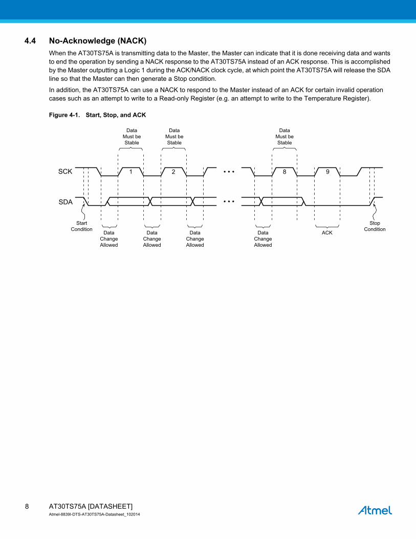
4.4 No-Acknowledge (NACK)
When the AT30TS75A is transmitting data to the Master, the Master can indicate that it is done receiving data and wants
to end the operation by sending a NACK response to the AT30TS75A instead of an ACK response. This is accomplished
by the Master outputting a Logic 1 during the ACK/NACK clock cycle, at which point the AT30TS75A will release the SDA
line so that the Master can then generate a Stop condition.
In addition, the AT30TS75A can use a NACK to respond to the Master instead of an ACK for certain invalid operation
cases such as an attempt to write to a Read-only Register (e.g. an attempt to write to the Temperature Register).
Figure 4-1. Start, Stop, and ACK
SCK
SDA
StartCondition
DataChangeAllowed
DataChangeAllowed
DataChangeAllowed
DataChangeAllowed
ACK
StopCondition
DataMust beStable
DataMust beStable
DataMust beStable
1 2 8 9
AT30TS75A [DATASHEET]Atmel-8839I-DTS-AT30TS75A-Datasheet_102014
8
5. Device Operation
Commands used to configure and control the operation of the AT30TS75A are sent to the device from the Master via the
serial interface. Likewise, the Master can read the temperature data from the AT30TS75A via the serial interface.
However, since multiple slave devices can reside on the serial bus, each slave device must have its own unique 7-bit
address so that the Master can access each device independently.
For the AT30TS75A, the first four MSBs of its 7-bit address are the device type identifier and are fixed at 1001. The
remaining three LSBs correspond to the states of the hard-wired A2-0 address pins.
Example: If the A2-0 pins are connected to GND, then the 7-bit device address would be 1001000.
In order for the Master to select and access the AT30TS75A, the Master must first initiate a Start condition. Following the
Start condition, the Master must output the device address byte. The device address byte consists of the 7-bit device
address plus a Read/Write (R/W) control bit, which indicates whether the Master will be performing a Read or a Write to
the AT30TS75A. If the R/W control bit is a Logic 1, then the Master will be reading data from the AT30TS75A.
Alternatively, if the R/W control bit is a Logic 0, then the Master will be writing data to the AT30TS75A.
Table 5-1. AT30TS75A Address Byte
If the 7-bit address sent by the Master matches that of the AT30TS75A, then the device will respond with an ACK after it
has received the full address byte. If there is an address mismatch, then the AT30TS75A will respond with a NACK and
return to the idle state.
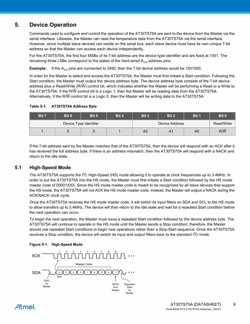
5.1 High-Speed Mode
The AT30TS75A supports the I2C High-Speed (HS) mode allowing it to operate at clock frequencies up to 3.4MHz. In
order to put the AT30TS75A into the HS mode, the Master must first initiate a Start condition followed by the HS mode
master code of 00001XXX. Since the HS mode master code is meant to be recognized by all slave devices that support
the HS mode, the AT30TS75A will not ACK the HS mode master code. Instead, the Master will output a NACK during the
ACK/NACK clock cycle.
Once the AT30TS75A receives the HS mode master code, it will switch its input filters on SDA and SCL to the HS mode
to allow transfers up to 3.4MHz. The device will then return to the idle state and wait for a repeated Start condition before
the next operation can occur.
To begin the next operation, the Master must issue a repeated Start condition followed by the device address byte. The
AT30TS75A will continue to operate in the HS mode until the Master sends a Stop condition; therefore, the Master
should use repeated Start conditions to begin new operations rather than a Stop-Start sequence. Once the AT30TS75A
receives a Stop condition, the device will switch its input and output filters back to the standard I2C mode.
Figure 5-1. High-Speed Mode
Bit 7 Bit 6 Bit 5 Bit 4 Bit 3 Bit 2 Bit 1 Bit 0
Device Type Identifier Device Address Read/Write
1 0 0 1 A2 A1 A0 R/W
SCK
SDA
Master Code
Startby
Master
MSB
NACKfrom
Master
RepeatedStartby
Master
1 2 3 4 5 6 7 8 9
0 0 0 0 1 X X X 1
9AT30TS75A [DATASHEET]Atmel-8839I-DTS-AT30TS75A-Datasheet_102014
5.2 Temperature Measurements
The AT30TS75A utilizes a band-gap type temperature sensor with an internal sigma-delta Analog-to-Digital Converter
(ADC) to measure and convert the temperature reading into a digital value with a selectable resolution as high as
0.0625C. The measured temperature is calibrated in degrees Celsius; therefore, a lookup table or conversion routine is
necessary for applications that wish to deal in degrees Fahrenheit.
The result of the digitized temperature measurements are stored in the internal Temperature Register of the
AT30TS75A, which is readable at any time through the device's serial interface. When in the normal operating mode, the
device performs continuous temperature measurements and updates the contents of the Temperature Register (see
Section 6.2, “Temperature Register” on page 16) after each analog-to-digital conversion.
The resolution of the temperature measurement data can be configured to 9, 10, 11, or 12 bits which corresponds to
temperature increments of 0.5C, 0.25C, 0.125C, and 0.0625C, respectively. Selecting the temperature resolution is
done using the R1 and R0 bits in the Configuration Register (see Section 6.3, “Configuration Register” on page 18). The
ADC conversion time does increase with each bit of higher resolution, so careful consideration should be given to the
resolution versus conversion time relationship. The default resolution after device power-up or reset is nine bits, which
retains backwards compatibility to industry-standard LM75-type devices.
With 12 bits of resolution, the AT30TS75A can theoretically measure a temperature range of 255C (-128C to +127C);
however, the device is only designed to measure temperatures over a range of -55C to +125C.
5.3 Temperature Alarm
After the measured temperature value has been stored into the Temperature Register, the data will be compared with
both the high and low temperature limits defined by the values stored in the THIGH Limit Register and TLOW Limit Register.
If the comparison results in a valid fault condition (see Section 5.3.1, “Fault Tolerance Limits” on page 10), then the
device will activate the ALERT output pin.
The polarity and function of the ALERT pin can be configured by using specific bits in the Configuration Register. The
ALERT pin defaults to the active low state after device power-up or reset but can be reconfigured to active high by setting
the POL bit in the Configuration Register to a Logic 1. The function of the ALERT pin changes based on the Alarm
Thermostat mode, which can be configured to either Comparator mode (see Section 5.3.2, “Comparator Mode” on page
11) or Interrupt mode (see Section 5.3.3, “Interrupt Mode” on page 12) by using the CMP/INT bit in the Configuration
Register. The Comparator mode is the default operating mode after the device powers up or resets.
The value of the high temperature limit stored in the THIGH Limit Register must be greater than the value of the low
temperature limit stored in the TLOW Limit Register in order for the ALERT function to work properly; otherwise, the
ALERT pin will output erroneous results and will falsely signal temperature alarms.
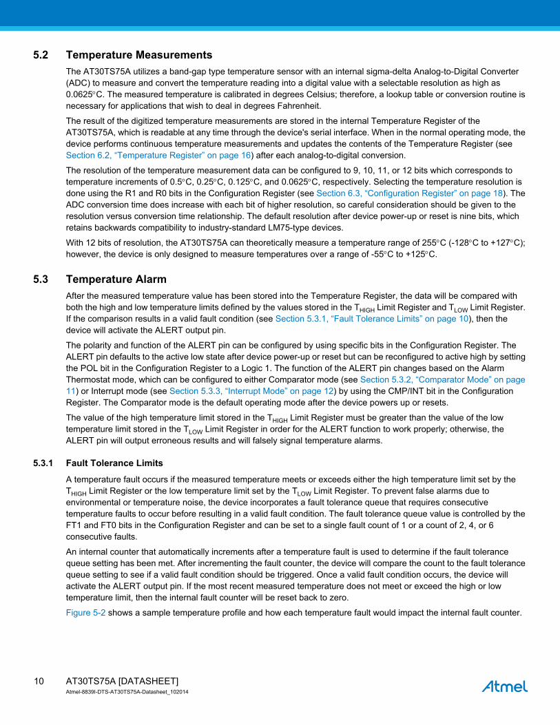
5.3.1 Fault Tolerance Limits
A temperature fault occurs if the measured temperature meets or exceeds either the high temperature limit set by the
THIGH Limit Register or the low temperature limit set by the TLOW Limit Register. To prevent false alarms due to
environmental or temperature noise, the device incorporates a fault tolerance queue that requires consecutive
temperature faults to occur before resulting in a valid fault condition. The fault tolerance queue value is controlled by the
FT1 and FT0 bits in the Configuration Register and can be set to a single fault count of 1 or a count of 2, 4, or 6
consecutive faults.
An internal counter that automatically increments after a temperature fault is used to determine if the fault tolerance
queue setting has been met. After incrementing the fault counter, the device will compare the count to the fault tolerance
queue setting to see if a valid fault condition should be triggered. Once a valid fault condition occurs, the device will
activate the ALERT output pin. If the most recent measured temperature does not meet or exceed the high or low
temperature limit, then the internal fault counter will be reset back to zero.
Figure 5-2 shows a sample temperature profile and how each temperature fault would impact the internal fault counter.
AT30TS75A [DATASHEET]Atmel-8839I-DTS-AT30TS75A-Datasheet_102014
10
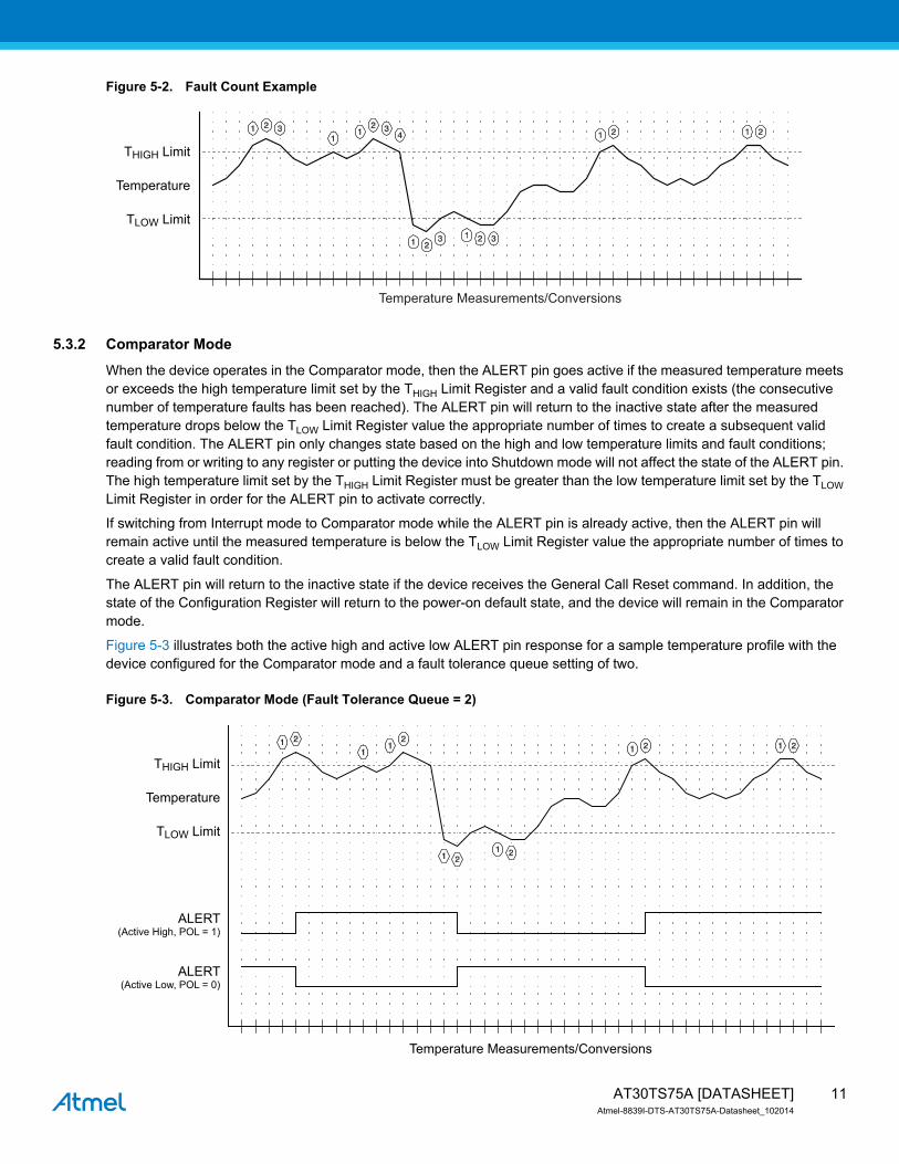
Figure 5-2. Fault Count Example
5.3.2 Comparator Mode
When the device operates in the Comparator mode, then the ALERT pin goes active if the measured temperature meets
or exceeds the high temperature limit set by the THIGH Limit Register and a valid fault condition exists (the consecutive
number of temperature faults has been reached). The ALERT pin will return to the inactive state after the measured
temperature drops below the TLOW Limit Register value the appropriate number of times to create a subsequent valid
fault condition. The ALERT pin only changes state based on the high and low temperature limits and fault conditions;
reading from or writing to any register or putting the device into Shutdown mode will not affect the state of the ALERT pin.
The high temperature limit set by the THIGH Limit Register must be greater than the low temperature limit set by the TLOW
Limit Register in order for the ALERT pin to activate correctly.
If switching from Interrupt mode to Comparator mode while the ALERT pin is already active, then the ALERT pin will
remain active until the measured temperature is below the TLOW Limit Register value the appropriate number of times to
create a valid fault condition.
The ALERT pin will return to the inactive state if the device receives the General Call Reset command. In addition, the
state of the Configuration Register will return to the power-on default state, and the device will remain in the Comparator
mode.
Figure 5-3 illustrates both the active high and active low ALERT pin response for a sample temperature profile with the
device configured for the Comparator mode and a fault tolerance queue setting of two.
Figure 5-3. Comparator Mode (Fault Tolerance Queue = 2)
Temperature Measurements/Conversions
THIGH Limit
Temperature
TLOW Limit
Temperature Measurements/Conversions
THIGH Limit
Temperature
TLOW Limit
ALERT(Active High, POL = 1)
ALERT(Active Low, POL = 0)
11AT30TS75A [DATASHEET]Atmel-8839I-DTS-AT30TS75A-Datasheet_102014
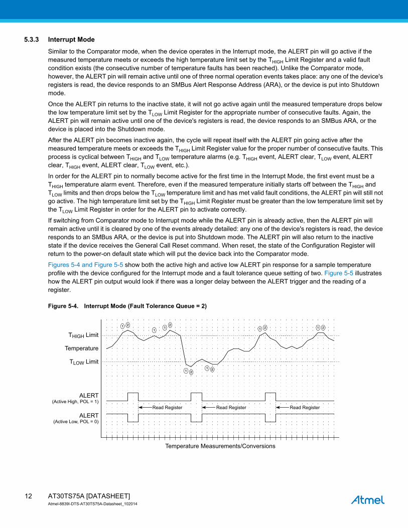
5.3.3 Interrupt Mode
Similar to the Comparator mode, when the device operates in the Interrupt mode, the ALERT pin will go active if the
measured temperature meets or exceeds the high temperature limit set by the THIGH Limit Register and a valid fault
condition exists (the consecutive number of temperature faults has been reached). Unlike the Comparator mode,
however, the ALERT pin will remain active until one of three normal operation events takes place: any one of the device's
registers is read, the device responds to an SMBus Alert Response Address (ARA), or the device is put into Shutdown
mode.
Once the ALERT pin returns to the inactive state, it will not go active again until the measured temperature drops below
the low temperature limit set by the TLOW Limit Register for the appropriate number of consecutive faults. Again, the
ALERT pin will remain active until one of the device's registers is read, the device responds to an SMBus ARA, or the
device is placed into the Shutdown mode.
After the ALERT pin becomes inactive again, the cycle will repeat itself with the ALERT pin going active after the
measured temperature meets or exceeds the THIGH Limit Register value for the proper number of consecutive faults. This
process is cyclical between THIGH and TLOW temperature alarms (e.g. THIGH event, ALERT clear, TLOW event, ALERT
clear, THIGH event, ALERT clear, TLOW event, etc.).
In order for the ALERT pin to normally become active for the first time in the Interrupt Mode, the first event must be a
THIGH temperature alarm event. Therefore, even if the measured temperature initially starts off between the THIGH and
TLOW limits and then drops below the TLOW temperature limit and has met valid fault conditions, the ALERT pin will still not
go active. The high temperature limit set by the THIGH Limit Register must be greater than the low temperature limit set by
the TLOW Limit Register in order for the ALERT pin to activate correctly.
If switching from Comparator mode to Interrupt mode while the ALERT pin is already active, then the ALERT pin will
remain active until it is cleared by one of the events already detailed: any one of the device's registers is read, the device
responds to an SMBus ARA, or the device is put into Shutdown mode. The ALERT pin will also return to the inactive
state if the device receives the General Call Reset command. When reset, the state of the Configuration Register will
return to the power-on default state which will put the device back into the Comparator mode.
Figures 5-4 and Figure 5-5 show both the active high and active low ALERT pin response for a sample temperature
profile with the device configured for the Interrupt mode and a fault tolerance queue setting of two. Figure 5-5 illustrates
how the ALERT pin output would look if there was a longer delay between the ALERT trigger and the reading of a
register.
Figure 5-4. Interrupt Mode (Fault Tolerance Queue = 2)
Temperature Measurements/Conversions
THIGH Limit
Temperature
TLOW Limit
ALERT(Active High, POL = 1)
ALERT(Active Low, POL = 0)
Read Register Read Register Read Register
AT30TS75A [DATASHEET]Atmel-8839I-DTS-AT30TS75A-Datasheet_102014
12

Figure 5-5. Interrupt Mode (Fault Tolerance Queue = 2) Delay Before Reading Register
5.4 Shutdown Mode
To reduce current consumption and save power, the device features a Shutdown mode that disables all internal device
circuitry except for the serial interface and POR circuits. While in the Shutdown mode, the internal temperature sensor is
not active, so no temperature measurements will be made. Entering and exiting the Shutdown mode is controlled by the
SD bit in the Configuration Register.
Entering the Shutdown mode can affect the ALERT pin depending on the Alarm Thermostat mode. If the device is
configured to operate in the Interrupt mode, then the ALERT pin will go inactive when the device enters the Shutdown
mode. However, the ALERT pin will not change states if the device is operating in the Comparator mode.
The fault count information will not change when the device enters or exits the Shutdown mode. Therefore, the number of
previous temperature faults recorded by the internal fault counter will be retained unless the device is power-cycled or
reset. When exiting the Shutdown mode, the ALERT pin will go active if operating in Interrupt mode, a valid fault
condition exists, and the THIGH and TLOW event cycles are maintained (i.e. THIGH event before entering Shutdown mode
followed by a TLOW event when exiting Shutdown mode).
5.4.1 One-Shot Mode
The AT30TS75A features a One-Shot Temperature mode that allows the device to perform a single temperature
measurement while in the Shutdown mode. By keeping the device in the Shutdown mode and utilizing the One-Shot
mode, the AT30TS75A can remain in a lower power state and only go active to take temperature measurements on an
as-needed basis. The internal fault counter will be updated when taking a temperature measurement using the
One-Shot mode; therefore, a valid fault condition can be generated by the One-Shot temperature measurements. If
operating in Comparator mode, then the fault condition will cause the ALERT pin to go either active or inactive depending
on if the fault condition is a result of a THIGH or TLOW event. If operating in Interrupt mode, the fault condition will cause the
ALERT pin to pulse active for a short duration of time to indicate a THIGH or TLOW event has occurred. The ALERT pin will
then return to the inactive state.
The One-Shot mode is controlled using the OS bit in the Configuration Register (see Section 6.3.1, “OS Bit” on page 19).
Temperature Measurements/Conversions
THIGH Limit
Temperature
TLOW Limit
ALERT(Active High, POL = 1)
ALERT(Active Low, POL = 0)
Read Register Read Register
13AT30TS75A [DATASHEET]Atmel-8839I-DTS-AT30TS75A-Datasheet_102014
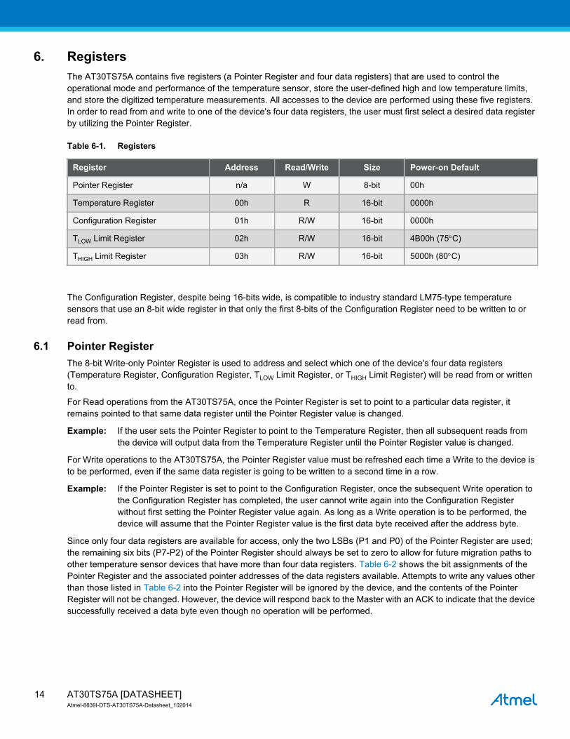
6. Registers
The AT30TS75A contains five registers (a Pointer Register and four data registers) that are used to control the
operational mode and performance of the temperature sensor, store the user-defined high and low temperature limits,
and store the digitized temperature measurements. All accesses to the device are performed using these five registers.
In order to read from and write to one of the device's four data registers, the user must first select a desired data register
by utilizing the Pointer Register.
Table 6-1. Registers
The Configuration Register, despite being 16-bits wide, is compatible to industry standard LM75-type temperature
sensors that use an 8-bit wide register in that only the first 8-bits of the Configuration Register need to be written to or
read from.
6.1 Pointer Register
The 8-bit Write-only Pointer Register is used to address and select which one of the device's four data registers
(Temperature Register, Configuration Register, TLOW Limit Register, or THIGH Limit Register) will be read from or written
to.
For Read operations from the AT30TS75A, once the Pointer Register is set to point to a particular data register, it
remains pointed to that same data register until the Pointer Register value is changed.
Example: If the user sets the Pointer Register to point to the Temperature Register, then all subsequent reads from
the device will output data from the Temperature Register until the Pointer Register value is changed.
For Write operations to the AT30TS75A, the Pointer Register value must be refreshed each time a Write to the device is
to be performed, even if the same data register is going to be written to a second time in a row.
Example: If the Pointer Register is set to point to the Configuration Register, once the subsequent Write operation to
the Configuration Register has completed, the user cannot write again into the Configuration Register
without first setting the Pointer Register value again. As long as a Write operation is to be performed, the
device will assume that the Pointer Register value is the first data byte received after the address byte.
Since only four data registers are available for access, only the two LSBs (P1 and P0) of the Pointer Register are used;
the remaining six bits (P7-P2) of the Pointer Register should always be set to zero to allow for future migration paths to
other temperature sensor devices that have more than four data registers. Table 6-2 shows the bit assignments of the
Pointer Register and the associated pointer addresses of the data registers available. Attempts to write any values other
than those listed in Table 6-2 into the Pointer Register will be ignored by the device, and the contents of the Pointer
Register will not be changed. However, the device will respond back to the Master with an ACK to indicate that the device
successfully received a data byte even though no operation will be performed.
Register Address Read/Write Size Power-on Default
Pointer Register n/a W 8-bit 00h
Temperature Register 00h R 16-bit 0000h
Configuration Register 01h R/W 16-bit 0000h
TLOW Limit Register 02h R/W 16-bit 4B00h (75C)
THIGH Limit Register 03h R/W 16-bit 5000h (80C)
AT30TS75A [DATASHEET]Atmel-8839I-DTS-AT30TS75A-Datasheet_102014
14
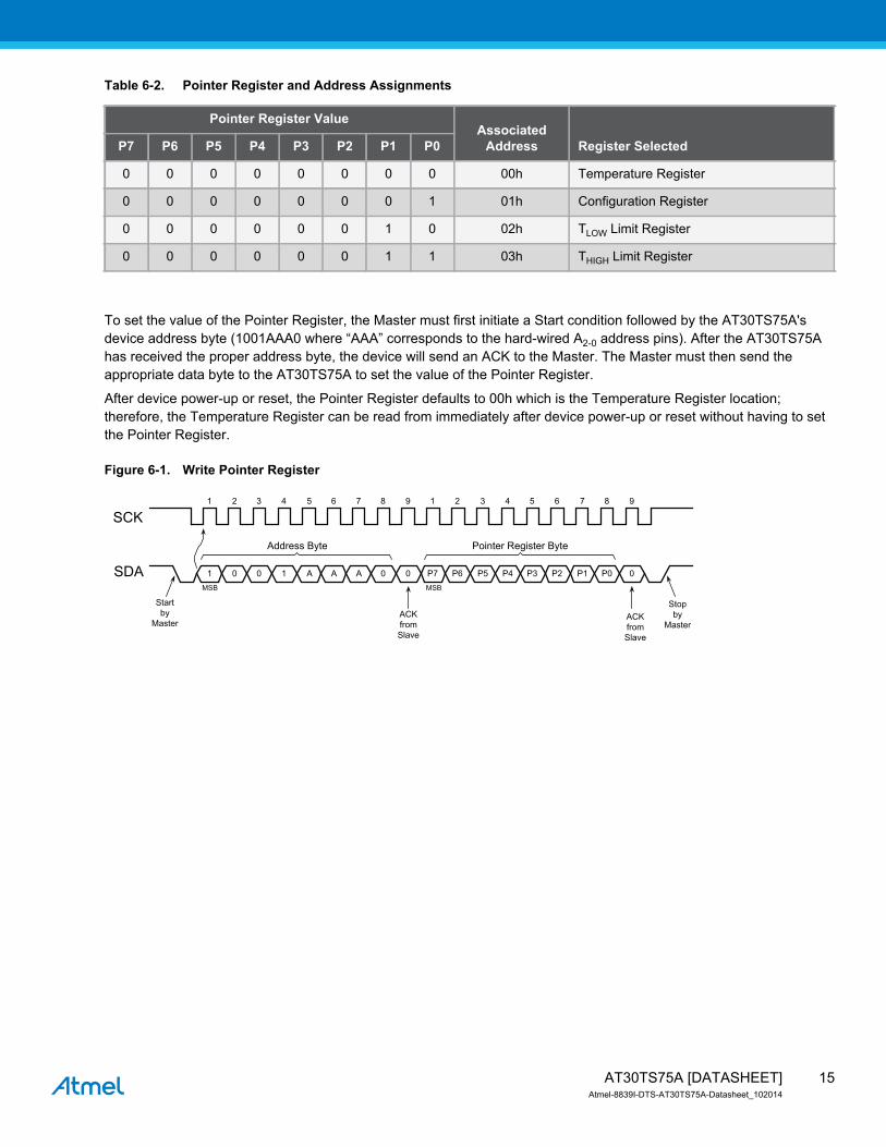
Table 6-2. Pointer Register and Address Assignments
To set the value of the Pointer Register, the Master must first initiate a Start condition followed by the AT30TS75A's
device address byte (1001AAA0 where “AAA” corresponds to the hard-wired A2-0 address pins). After the AT30TS75A
has received the proper address byte, the device will send an ACK to the Master. The Master must then send the
appropriate data byte to the AT30TS75A to set the value of the Pointer Register.
After device power-up or reset, the Pointer Register defaults to 00h which is the Temperature Register location;
therefore, the Temperature Register can be read from immediately after device power-up or reset without having to set
the Pointer Register.
Figure 6-1. Write Pointer Register
Pointer Register ValueAssociated
Address Register SelectedP7 P6 P5 P4 P3 P2 P1 P0
0 0 0 0 0 0 0 0 00h Temperature Register
0 0 0 0 0 0 0 1 01h Configuration Register
0 0 0 0 0 0 1 0 02h TLOW Limit Register
0 0 0 0 0 0 1 1 03h THIGH Limit Register
SCK
SDA
Address Byte Pointer Register Byte
Startby
MasterACKfromSlave
MSB MSB
ACKfromSlave
Stopby
Master
1 0 0 1 A A A 0 0 P7 P6 P5 P4 P3 P2 P1 P0 0
1 2 3 4 5 6 7 8 9 1 2 3 4 5 6 7 8 9
15AT30TS75A [DATASHEET]Atmel-8839I-DTS-AT30TS75A-Datasheet_102014
6.2 Temperature Register
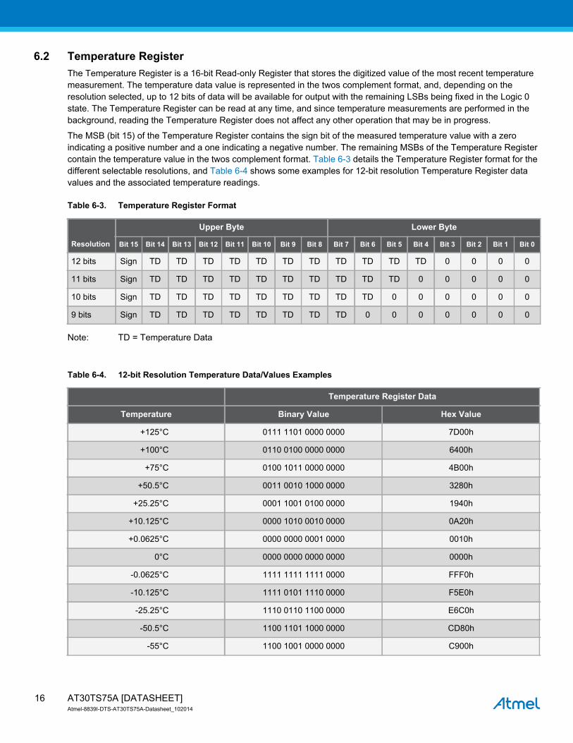
The Temperature Register is a 16-bit Read-only Register that stores the digitized value of the most recent temperature
measurement. The temperature data value is represented in the twos complement format, and, depending on the
resolution selected, up to 12 bits of data will be available for output with the remaining LSBs being fixed in the Logic 0
state. The Temperature Register can be read at any time, and since temperature measurements are performed in the
background, reading the Temperature Register does not affect any other operation that may be in progress.
The MSB (bit 15) of the Temperature Register contains the sign bit of the measured temperature value with a zero
indicating a positive number and a one indicating a negative number. The remaining MSBs of the Temperature Register
contain the temperature value in the twos complement format. Table 6-3 details the Temperature Register format for the
different selectable resolutions, and Table 6-4 shows some examples for 12-bit resolution Temperature Register data
values and the associated temperature readings.
Table 6-3. Temperature Register Format
Note: TD = Temperature Data
Table 6-4. 12-bit Resolution Temperature Data/Values Examples
Resolution
Upper Byte Lower Byte
Bit 15 Bit 14 Bit 13 Bit 12 Bit 11 Bit 10 Bit 9 Bit 8 Bit 7 Bit 6 Bit 5 Bit 4 Bit 3 Bit 2 Bit 1 Bit 0
12 bits Sign TD TD TD TD TD TD TD TD TD TD TD 0 0 0 0
11 bits Sign TD TD TD TD TD TD TD TD TD TD 0 0 0 0 0
10 bits Sign TD TD TD TD TD TD TD TD TD 0 0 0 0 0 0
9 bits Sign TD TD TD TD TD TD TD TD 0 0 0 0 0 0 0
Temperature Register Data
Temperature Binary Value Hex Value
+125°C 0111 1101 0000 0000 7D00h
+100°C 0110 0100 0000 0000 6400h
+75°C 0100 1011 0000 0000 4B00h
+50.5°C 0011 0010 1000 0000 3280h
+25.25°C 0001 1001 0100 0000 1940h
+10.125°C 0000 1010 0010 0000 0A20h
+0.0625°C 0000 0000 0001 0000 0010h
0°C 0000 0000 0000 0000 0000h
-0.0625°C 1111 1111 1111 0000 FFF0h
-10.125°C 1111 0101 1110 0000 F5E0h
-25.25°C 1110 0110 1100 0000 E6C0h
-50.5°C 1100 1101 1000 0000 CD80h
-55°C 1100 1001 0000 0000 C900h
AT30TS75A [DATASHEET]Atmel-8839I-DTS-AT30TS75A-Datasheet_102014
16
After each temperature measurement and digital conversion is complete, the new temperature data is loaded into the
Temperature Register if the register is not currently being read. If a Read is in progress, then the previous temperature
data will be output.
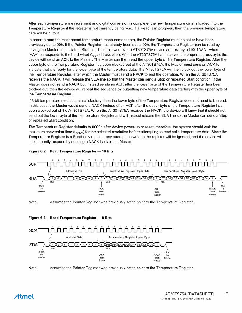
In order to read the most recent temperature measurement data, the Pointer Register must be set or have been
previously set to 00h. If the Pointer Register has already been set to 00h, the Temperature Register can be read by
having the Master first initiate a Start condition followed by the AT30TS75A device address byte (1001AAA1 where
“AAA” corresponds to the hard-wired A2-0 address pins). After the AT30TS75A has received the proper address byte, the
device will send an ACK to the Master. The Master can then read the upper byte of the Temperature Register. After the
upper byte of the Temperature Register has been clocked out of the AT30TS75A, the Master must send an ACK to
indicate that it is ready for the lower byte of the temperature data. The AT30TS75A will then clock out the lower byte of
the Temperature Register, after which the Master must send a NACK to end the operation. When the AT30TS75A
receives the NACK, it will release the SDA line so that the Master can send a Stop or repeated Start condition. If the
Master does not send a NACK but instead sends an ACK after the lower byte of the Temperature Register has been
clocked out, then the device will repeat the sequence by outputting new temperature data starting with the upper byte of
the Temperature Register.
If 8-bit temperature resolution is satisfactory, then the lower byte of the Temperature Register does not need to be read.
In this case, the Master would send a NACK instead of an ACK after the upper byte of the Temperature Register has
been clocked out of the AT30TS75A. When the AT30TS75A receives the NACK, the device will know that it should not
send out the lower byte of the Temperature Register and will instead release the SDA line so the Master can send a Stop
or repeated Start condition.
The Temperature Register defaults to 0000h after device power-up or reset; therefore, the system should wait the
maximum conversion time (tCONV) for the selected resolution before attempting to read valid temperature data. Since the
Temperature Register is a Read-only register, any attempts to write to the register will be ignored, and the device will
subsequently respond by sending a NACK back to the Master.
Figure 6-2. Read Temperature Register — 16 Bits
Note: Assumes the Pointer Register was previously set to point to the Temperature Register.
Figure 6-3. Read Temperature Register — 8 Bits
Note: Assumes the Pointer Register was previously set to point to the Temperature Register.
SCK
SDA
Address Byte Temperature Register Upper Byte Temperature Register Lower Byte
Startby
MasterACKfromSlave
ACKfrom
Master
MSB MSB
NACKfrom
Master
Stopby
Master
MSB
1 2 3 4 5 6 7 8 9 1 2 3 4 5 6 7 8 9 1 2 3 4 5 6 7 8 9
1 0 0 1 A A A 1 0 D15 D14 D13 D12 D11 D10 D9 D8 0 D7 D6 D5 D4 D3 D2 D1 D0 1
SCK
SDA
Address Byte Temperature Register Upper Byte
Startby
MasterACKfromSlave
MSB MSB
NACKfrom
Master
Stopby
Master
1 2 3 4 5 6 7 8 9 1 2 3 4 5 6 7 8 9
1 0 0 1 A A A 1 0 D15 D14 D13 D12 D11 D10 D9 D8 1
17AT30TS75A [DATASHEET]Atmel-8839I-DTS-AT30TS75A-Datasheet_102014
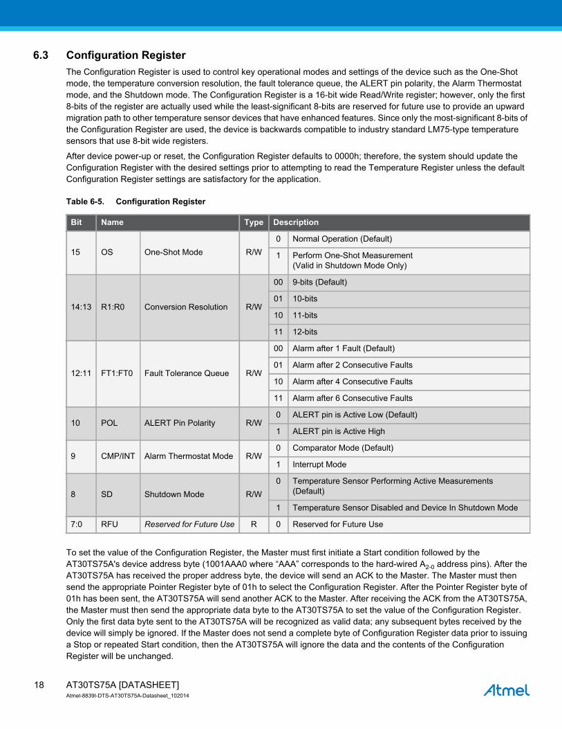
6.3 Configuration Register
The Configuration Register is used to control key operational modes and settings of the device such as the One-Shot
mode, the temperature conversion resolution, the fault tolerance queue, the ALERT pin polarity, the Alarm Thermostat
mode, and the Shutdown mode. The Configuration Register is a 16-bit wide Read/Write register; however, only the first
8-bits of the register are actually used while the least-significant 8-bits are reserved for future use to provide an upward
migration path to other temperature sensor devices that have enhanced features. Since only the most-significant 8-bits of
the Configuration Register are used, the device is backwards compatible to industry standard LM75-type temperature
sensors that use 8-bit wide registers.
After device power-up or reset, the Configuration Register defaults to 0000h; therefore, the system should update the
Configuration Register with the desired settings prior to attempting to read the Temperature Register unless the default
Configuration Register settings are satisfactory for the application.
Table 6-5. Configuration Register
To set the value of the Configuration Register, the Master must first initiate a Start condition followed by the
AT30TS75A's device address byte (1001AAA0 where “AAA” corresponds to the hard-wired A2-0 address pins). After the
AT30TS75A has received the proper address byte, the device will send an ACK to the Master. The Master must then
send the appropriate Pointer Register byte of 01h to select the Configuration Register. After the Pointer Register byte of
01h has been sent, the AT30TS75A will send another ACK to the Master. After receiving the ACK from the AT30TS75A,
the Master must then send the appropriate data byte to the AT30TS75A to set the value of the Configuration Register.
Only the first data byte sent to the AT30TS75A will be recognized as valid data; any subsequent bytes received by the
device will simply be ignored. If the Master does not send a complete byte of Configuration Register data prior to issuing
a Stop or repeated Start condition, then the AT30TS75A will ignore the data and the contents of the Configuration
Register will be unchanged.
Bit Name Type Description
15 OS One-Shot Mode R/W
0 Normal Operation (Default)
1 Perform One-Shot Measurement
(Valid in Shutdown Mode Only)
14:13 R1:R0 Conversion Resolution R/W
00 9-bits (Default)
01 10-bits
10 11-bits
11 12-bits
12:11 FT1:FT0 Fault Tolerance Queue R/W
00 Alarm after 1 Fault (Default)
01 Alarm after 2 Consecutive Faults
10 Alarm after 4 Consecutive Faults
11 Alarm after 6 Consecutive Faults
10 POL ALERT Pin Polarity R/W0 ALERT pin is Active Low (Default)
1 ALERT pin is Active High
9 CMP/INT Alarm Thermostat Mode R/W0 Comparator Mode (Default)
1 Interrupt Mode
8 SD Shutdown Mode R/W
0 Temperature Sensor Performing Active Measurements
(Default)
1 Temperature Sensor Disabled and Device In Shutdown Mode
7:0 RFU Reserved for Future Use R 0 Reserved for Future Use
AT30TS75A [DATASHEET]Atmel-8839I-DTS-AT30TS75A-Datasheet_102014
18
6.3.1 OS Bit
The OS bit is used to enable the One-Shot Temperature Measurement mode. When a Logic 1 is written to the OS bit
while the AT30TS75A is in the Shutdown mode, the device will become active and perform a single temperature
measurement and conversion. After the Temperature Register has been updated with the measured temperature data,
the device will return to the low-power Shutdown mode and clear the OS bit.
Writing a one to the OS bit when the device is not in the Shutdown mode will have no affect. When reading the
Configuration Register, the OS bit will always be read as a Logic 0.
6.3.2 R1:R0 Bits
The R1 and R0 bits are used to select the conversion resolution of the internal sigma-delta ADC. Four possible
resolutions can be set to maximize for either higher resolution or faster conversion times. The R1 and R0 bits default to
the Logic 0 state after device power-up or reset to retain backwards compatibility to industry-standard LM75-type
devices.
Table 6-6. Conversion Resolution
6.3.3 FT1:FT0 Bits
The FT1 and FT0 bits are used to set the fault tolerance queue value which defines how many consecutive faults must
occur before the ALERT pin will be activated (see Section 5.3.1, “Fault Tolerance Limits” on page 10). The FT1 and FT0
bit settings provide four different fault values as detailed in Table 6-7. After the device powers up or resets, both the FT1
and FT0 bits will default to the Logic 0 state.
Table 6-7. Fault Tolerance Queue
6.3.4 POL Bit
The ALERT pin polarity is controlled by the POL bit. When the POL bit is in the Logic 0 state, the ALERT pin will be an
active low output (the default setting after device power-up or reset). To configure the ALERT pin as an active high
output, the POL bit must be set to the Logic 1 state.
R1 R0 Conversion Resolution Conversion Time
0 0 9 bits 0.5°C 25ms
0 1 10 bits 0.25°C 50ms
1 0 11 bits 0.125°C 100ms
1 1 12 bits 0.0625°C 200ms
NVFT1 NVFT0 Consecutive Faults Required
0 0 1
0 1 2
1 0 4
1 1 6
19AT30TS75A [DATASHEET]Atmel-8839I-DTS-AT30TS75A-Datasheet_102014
6.3.5 CMP/INT Bit
The CMP/INT bit controls whether the device will operate in the Comparator mode or the Interrupt mode. Setting the
CMP/INT bit to the Logic 0 state will put the device into the Comparator mode (default after device power-up or reset).
Alternatively, when the CMP/INT bit is set to the Logic 1 state, then the device will operate in the Interrupt mode. The
function of the ALERT pin changes based on the CMP/INT bit setting.
6.3.6 SD Bit
The SD bit is used to enable or disable the device's Shutdown mode. When the SD bit is in the Logic 0 state (default after
device power-up or reset), the device will be in the normal operational mode and perform continuous temperature
measurements and conversions. When the SD bit is set to the Logic 1 state, the device will finish the current temperature
measurement and conversion and will store the result in the Temperature Register, after which the device will then enter
the Shutdown mode.
Resetting the SD bit back to a Logic 0 will return the device to the normal operating mode.
Figure 6-4. Write to Configuration Register
Figure 6-5. Read from Configuration Register
Note: Assumes the Pointer Register was previously set to point to the Configuration Register.
SCK
SDA
Address Byte Pointer Register Byte Configuration Register Upper Byte
Startby
MasterACKfromSlave
ACKfromSlave
MSB MSB
ACKfromSlave
Stopby
Master
MSB
1 2 3 4 5 6 7 8 9 1 2 3 4 5 6 7 8 9 1 2 3 4 5 6 7 8 9
1 0 0 1 A A A 0 0 0 0 0 0 0 0 0 1 0 D15 D14 D13 D12 D11 D10 D9 D8 0
SCK
SDAStartby
MasterACKfromSlave
NACKfrom
Master
Address Byte Configuration Register Upper Byte
Stopby
Master
MSB MSB
1 2 3 4 5 6 7 8 9 1 2 3 4 5 6 7 8 9
1 0 0 1 A A A 1 0 D15 D14 D13 D12 D11 D10 D9 D8 1
AT30TS75A [DATASHEET]Atmel-8839I-DTS-AT30TS75A-Datasheet_102014
20
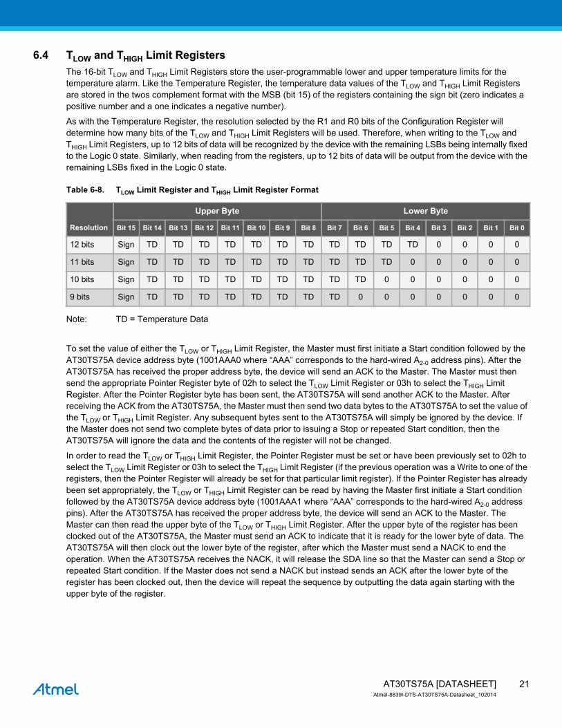
6.4 TLOW and THIGH Limit Registers
The 16-bit TLOW and THIGH Limit Registers store the user-programmable lower and upper temperature limits for the
temperature alarm. Like the Temperature Register, the temperature data values of the TLOW and THIGH Limit Registers
are stored in the twos complement format with the MSB (bit 15) of the registers containing the sign bit (zero indicates a
positive number and a one indicates a negative number).
As with the Temperature Register, the resolution selected by the R1 and R0 bits of the Configuration Register will
determine how many bits of the TLOW and THIGH Limit Registers will be used. Therefore, when writing to the TLOW and
THIGH Limit Registers, up to 12 bits of data will be recognized by the device with the remaining LSBs being internally fixed
to the Logic 0 state. Similarly, when reading from the registers, up to 12 bits of data will be output from the device with the
remaining LSBs fixed in the Logic 0 state.
Table 6-8. TLOW Limit Register and THIGH Limit Register Format
Note: TD = Temperature Data
To set the value of either the TLOW or THIGH Limit Register, the Master must first initiate a Start condition followed by the
AT30TS75A device address byte (1001AAA0 where “AAA” corresponds to the hard-wired A2-0 address pins). After the
AT30TS75A has received the proper address byte, the device will send an ACK to the Master. The Master must then
send the appropriate Pointer Register byte of 02h to select the TLOW Limit Register or 03h to select the THIGH Limit
Register. After the Pointer Register byte has been sent, the AT30TS75A will send another ACK to the Master. After
receiving the ACK from the AT30TS75A, the Master must then send two data bytes to the AT30TS75A to set the value of
the TLOW or THIGH Limit Register. Any subsequent bytes sent to the AT30TS75A will simply be ignored by the device. If
the Master does not send two complete bytes of data prior to issuing a Stop or repeated Start condition, then the
AT30TS75A will ignore the data and the contents of the register will not be changed.
In order to read the TLOW or THIGH Limit Register, the Pointer Register must be set or have been previously set to 02h to
select the TLOW Limit Register or 03h to select the THIGH Limit Register (if the previous operation was a Write to one of the
registers, then the Pointer Register will already be set for that particular limit register). If the Pointer Register has already
been set appropriately, the TLOW or THIGH Limit Register can be read by having the Master first initiate a Start condition
followed by the AT30TS75A device address byte (1001AAA1 where “AAA” corresponds to the hard-wired A2-0 address
pins). After the AT30TS75A has received the proper address byte, the device will send an ACK to the Master. The
Master can then read the upper byte of the TLOW or THIGH Limit Register. After the upper byte of the register has been
clocked out of the AT30TS75A, the Master must send an ACK to indicate that it is ready for the lower byte of data. The
AT30TS75A will then clock out the lower byte of the register, after which the Master must send a NACK to end the
operation. When the AT30TS75A receives the NACK, it will release the SDA line so that the Master can send a Stop or
repeated Start condition. If the Master does not send a NACK but instead sends an ACK after the lower byte of the
register has been clocked out, then the device will repeat the sequence by outputting the data again starting with the
upper byte of the register.
Resolution
Upper Byte Lower Byte
Bit 15 Bit 14 Bit 13 Bit 12 Bit 11 Bit 10 Bit 9 Bit 8 Bit 7 Bit 6 Bit 5 Bit 4 Bit 3 Bit 2 Bit 1 Bit 0
12 bits Sign TD TD TD TD TD TD TD TD TD TD TD 0 0 0 0
11 bits Sign TD TD TD TD TD TD TD TD TD TD 0 0 0 0 0
10 bits Sign TD TD TD TD TD TD TD TD TD 0 0 0 0 0 0
9 bits Sign TD TD TD TD TD TD TD TD 0 0 0 0 0 0 0
21AT30TS75A [DATASHEET]Atmel-8839I-DTS-AT30TS75A-Datasheet_102014
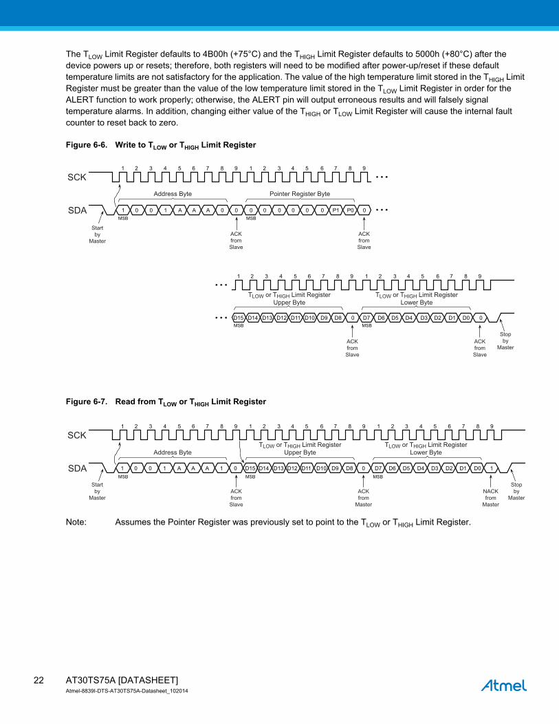
The TLOW Limit Register defaults to 4B00h (+75°C) and the THIGH Limit Register defaults to 5000h (+80°C) after the
device powers up or resets; therefore, both registers will need to be modified after power-up/reset if these default
temperature limits are not satisfactory for the application. The value of the high temperature limit stored in the THIGH Limit
Register must be greater than the value of the low temperature limit stored in the TLOW Limit Register in order for the
ALERT function to work properly; otherwise, the ALERT pin will output erroneous results and will falsely signal
temperature alarms. In addition, changing either value of the THIGH or TLOW Limit Register will cause the internal fault
counter to reset back to zero.
Figure 6-6. Write to TLOW or THIGH Limit Register
Figure 6-7. Read from TLOW or THIGH Limit Register
Note: Assumes the Pointer Register was previously set to point to the TLOW or THIGH Limit Register.
SCK
SDA
Startby
MasterACKfromSlave
ACKfromSlave
Address Byte
TLOW or THIGH Limit RegisterUpper Byte
TLOW or THIGH Limit RegisterLower Byte
Pointer Register Byte
MSB MSB
ACKfromSlave
ACKfromSlave
Stopby
Master
MSB MSB
1 2 3 4 5 6 7 8 9 1 2 3 4 5 6 7 8 9
1 0 0 1 A A A 0 0 0 0 0 0 0 0 P1 P0 0
1 2 3 4 5 6 7 8 9 1 2 3 4 5 6 7 8 9
D15 D14 D13 D12 D11 D10 D9 D8 0 D7 D6 D5 D4 D3 D2 D1 D0 0
SCK
SDAStartby
MasterACKfromSlave
NACKfrom
Master
Stopby
MasterACKfrom
Master
Address ByteTLOW or THIGH Limit Register
Upper ByteTLOW or THIGH Limit Register
Lower Byte
1 2 3 4 5 6 7 8 9 1 2 3 4 5 6 7 8 9 1 2 3 4 5 6 7 8 9
1 0 0 1 A A A 1 0 D15 D14 D13 D12 D11 D10 D9 D8 0 D7 D6 D5 D4 D3 D2 D1 D0 1MSB MSB MSB
AT30TS75A [DATASHEET]Atmel-8839I-DTS-AT30TS75A-Datasheet_102014
22
7. SMBus Features and I2C General Call
7.1 SMBus Alert
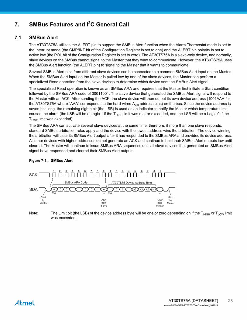
The AT30TS75A utilizes the ALERT pin to support the SMBus Alert function when the Alarm Thermostat mode is set to
the Interrupt mode (the CMP/INT bit of the Configuration Register is set to one) and the ALERT pin polarity is set to
active low (the POL bit of the Configuration Register is set to zero). The AT30TS75A is a slave-only device, and normally,
slave devices on the SMBus cannot signal to the Master that they want to communicate. However, the AT30TS75A uses
the SMBus Alert function (the ALERT pin) to signal to the Master that it wants to communicate.
Several SMBus Alert pins from different slave devices can be connected to a common SMBus Alert input on the Master.
When the SMBus Alert input on the Master is pulled low by one of the slave devices, the Master can perform a
specialized Read operation from the slave devices to determine which device sent the SMBus Alert signal.
The specialized Read operation is known as an SMBus ARA and requires that the Master first initiate a Start condition
followed by the SMBus ARA code of 00011001. The slave device that generated the SMBus Alert signal will respond to
the Master with an ACK. After sending the ACK, the slave device will then output its own device address (1001AAA for
the AT30TS75A where “AAA” corresponds to the hard-wired A2-0 address pins) on the bus. Since the device address is
seven bits long, the remaining eighth bit (the LSB) is used as an indicator to notify the Master which temperature limit
caused the alarm (the LSB will be a Logic 1 if the THIGH limit was met or exceeded, and the LSB will be a Logic 0 if the
TLOW limit was exceeded).
The SMBus ARA can activate several slave devices at the same time; therefore, if more than one slave responds,
standard SMBus arbitration rules apply and the device with the lowest address wins the arbitration. The device winning
the arbitration will clear its SMBus Alert output after it has responded to the SMBus ARA and provided its device address.
All other devices with higher addresses do not generate an ACK and continue to hold their SMBus Alert outputs low until
cleared. The Master will continue to issue SMBus ARA sequences until all slave devices that generated an SMBus Alert
signal have responded and cleared their SMBus Alert outputs.
Figure 7-1. SMBus Alert
Note: The Limit bit (the LSB) of the device address byte will be one or zero depending on if the THIGH or TLOW limit
was exceeded.
SCK
SDA
SMBus ARA Code AT30TS75 Device Address Byte
Startby
MasterACKfromSlave
NACKfrom
Master
Stopby
Master
MSB MSB 0 0 0 1 1 0 0 1 0 1 0 0 1 A2 A1 A0 Limit 1
1 2 3 4 5 6 7 8 9 1 2 3 4 5 6 7 8 9
23AT30TS75A [DATASHEET]Atmel-8839I-DTS-AT30TS75A-Datasheet_102014
7.2 SMBus Timeout
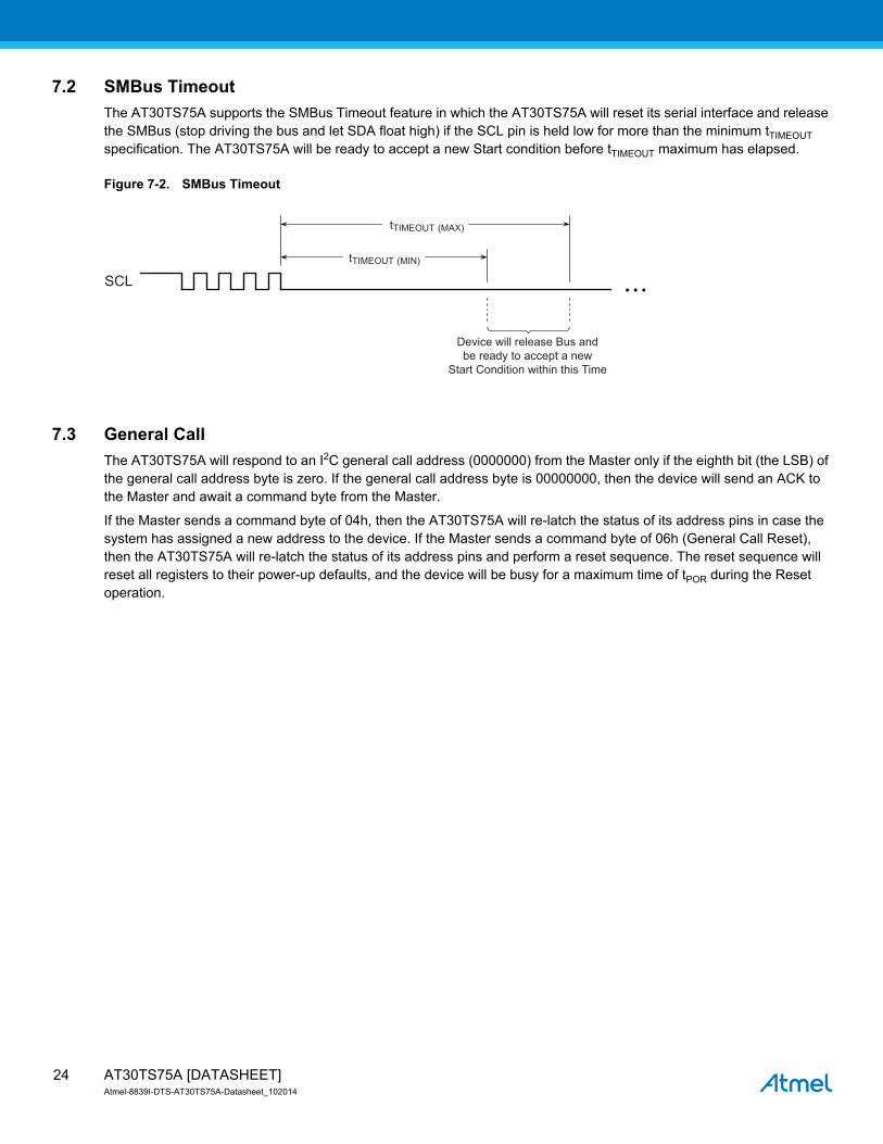
The AT30TS75A supports the SMBus Timeout feature in which the AT30TS75A will reset its serial interface and release
the SMBus (stop driving the bus and let SDA float high) if the SCL pin is held low for more than the minimum tTIMEOUT
specification. The AT30TS75A will be ready to accept a new Start condition before tTIMEOUT maximum has elapsed.
Figure 7-2. SMBus Timeout
7.3 General Call
The AT30TS75A will respond to an I2C general call address (0000000) from the Master only if the eighth bit (the LSB) of
the general call address byte is zero. If the general call address byte is 00000000, then the device will send an ACK to
the Master and await a command byte from the Master.
If the Master sends a command byte of 04h, then the AT30TS75A will re-latch the status of its address pins in case the
system has assigned a new address to the device. If the Master sends a command byte of 06h (General Call Reset),
then the AT30TS75A will re-latch the status of its address pins and perform a reset sequence. The reset sequence will
reset all registers to their power-up defaults, and the device will be busy for a maximum time of tPOR during the Reset
operation.
Device will release Bus andbe ready to accept a new
Start Condition within this Time
tTIMEOUT (MAX)
tTIMEOUT (MIN)
SCL
AT30TS75A [DATASHEET]Atmel-8839I-DTS-AT30TS75A-Datasheet_102014
24
8. Electrical Specifications
8.1 Absolute Maximum Ratings*
8.2 DC and AC Operating Range
Notes: 1. Device operation is guaranteed from -40°C to +125°C.
2. Device operation is not guaranteed at -55°C but ensured by characterization.
Temperature under Bias . . . . . . . -40°C to +125°C
Storage Temperature . . . . . . . . . -65°C to +150°C
Supply voltage
with respect to ground . . . . . . . . . . . -0.5V to +7.0V
ALERT Pin . . . . . . . . . . . . . . . -0.5V to VCC + 0.3V
All input voltages
with respect to ground . . . . . . . -0.5V to VCC + 0.5V
All other output voltages
with respect to ground . . . . . . . -0.5V to VCC + 0.5V
*Notice: Stresses beyond those listed under “Absolute Maximum
Ratings” may cause permanent damage to the device.
Functional operation of the device at these ratings or any
other conditions beyond those indicated in the operational
sections of this specification is not implied. Exposure to
absolute maximum rating conditions for extended periods
may affect device reliability. Voltage extremes referenced
in the “Absolute Maximum Ratings” are intended to
accommodate short duration undershoot/overshoot
conditions and does not imply or guarantee functional
device operation at these levels for any extended period of
time.
Pull-up voltages applied to the ALERT pin that exceed the
“Absolute Maximum Ratings” may forward bias to the ESD
protection circuitry. Doing so may result in improper device
function and may corrupt temperature measurements.
AT30TS75A
Operating Temperature (Case) Industrial High Temperature -55C to +125C(1)(2)
VCC Power Supply 1.7V to 5.5V
25AT30TS75A [DATASHEET]Atmel-8839I-DTS-AT30TS75A-Datasheet_102014

8.3 DC Characteristics
Note: 1. Typical values characterized at TA = +25°C at VCC = 1.8V, 3.0V and 5.0V unless otherwise noted.
Symbol Parameter VCC Range Condition Min Typ(1) Max Units
ICC1
Active Current,
Bus Inactive
1.7V ≤ VCC ≤ 2.0V
Active Temperature
Conversions
60 85
μA2.7V ≤ VCC ≤ 3.6V 65 95
4.5V ≤ VCC ≤ 5.5V 85 125
ICC2
Active Current,
Bus Active
1.7V ≤ VCC ≤ 2.0VActive Temperature
Conversions,
fSCL = 400kHz
120 160
μA2.7V ≤ VCC ≤ 3.6V 150 225
4.5V ≤ VCC ≤ 5.5V 225 325
ICC3
Active Current,
Bus Active
2.2V ≤ VCC ≤ 3.6V Active Temperature
Conversions,
fSCL = 3.4MHz
235 500
μA4.5V ≤ VCC ≤ 5.5V 610 800
ISD1
Shutdown Mode
Current, Bus Inactive
1.7V ≤ VCC ≤ 2.0V 0.4 2.5
μA2.7V ≤ VCC ≤ 3.6V 0.6 3.5
4.5V ≤ VCC ≤ 5.5V 1.2 5.5
ISD2
Shutdown Mode
Current, Bus Active
1.7V ≤ VCC ≤ 2.0V
fSCL = 400kHz
110 160
μA2.7V ≤ VCC ≤ 3.6V 130 200
4.5V ≤ VCC ≤ 5.5V 180 280
ISD3
Shutdown Mode
Current, Bus Active
2.2V ≤ VCC ≤ 3.6VfSCL = 3.4MHz
210 425μA
4.5V ≤ VCC ≤ 5.5V 550 750
ILI Input Leakage Current VIN = CMOS levels ±1 μA
ILO
Output Leakage
CurrentVOUT = CMOS levels ±1 μA
VIL Input Low Voltage 0.3 x VCC V
VIH Input High Voltage 0.7 x VCC V
VOL1 Output Low Voltage IOL = 3mA 0.4 V
VOL2
Output Low Voltage,
ALERT PinIOL = 4mA 0.4 V
AT30TS75A [DATASHEET]Atmel-8839I-DTS-AT30TS75A-Datasheet_102014
26
8.4 Temperature Sensor Accuracy and Conversion Characteristics
Notes: 1. Typical values characterized at VCC = 3.3V, TA = +25°C unless otherwise noted.
2. Sensor accuracy characterized to this range but not tested or guaranteed.
8.5 AC Characteristics
Notes: 1. These parameters are determined through product characterization and are not tested 100% in production.
2. Minimum clock frequency must be at least 1kHz to avoid activating the SMBus timeout feature.
Symbol Parameter Condition Min Typ(1) Max Units
TACC Sensor Accuracy
TA = 0°C to +85°C ±0.5 ±1.0
CTA = -25°C to +105°C ±1.0 ±2.0
TA = -40°C to +125°C ±2.0 ±3.0
TA = -55°C to +125°C(2) ±3.0
TRES Conversion Resolution Selectable 9 to 12 bits 0.5 (9 bits) 0.0625 (12 bits) C
tCONV Conversion Time
9-bit Resolution 25 37.5
ms10-bit Resolution 50 75
11-bit Resolution 100 150
12-bit Resolution 200 300
Symbol Parameter
VCC = 1.7V to 3.6V VCC < 2.2V VCC = 2.2V to 3.6V
Units
Fast Mode Fast Mode Plus High-Speed Mode
Min Max Min Max Min Max
fSCL Serial Clock Frequency 1(2) 400 1(2) 1000 1(2) 3400 kHz
tSCLH Clock High Time 600 260 60 ns
tSCLL Clock Low Time 1300 500 160 ns
tR Clock/Data Input Rise Time(8-1) 300 120 100 ns
tF Clock/Data Input Fall Time(8-1) 300 120 100 ns
tSUDAT Data In Setup Time 100 50 10 ns
tHDDAT Data In Hold Time 0 0 0 ns
tV Output Valid Time 900 350 80 ns
tOH Output Hold Time 0 0 0 ns
tBUF
Bus Free Time Between Stop and Start
Condition1300 500 160 ns
tSUSTA
Repeated Start Condition Setup Time (SCL
High to SDA Low)100 50 50 ns
tHDSTA
Start Condition Hold Time (SDA Low to
SCL Low)100 50 50 ns
tSUSTO
Stop Condition Setup Time (SCL High to
SDA High)600 50 50 ns
tNS Noise Suppression Input Filter Time 100 50 10 ns
tTIMEOUT SMBus Timeout Time 25 75 25 75 25 75 ms
CLOAD Capacitive Load for SCL and SDA Lines(8-1) 400 400 100 pF
27AT30TS75A [DATASHEET]Atmel-8839I-DTS-AT30TS75A-Datasheet_102014
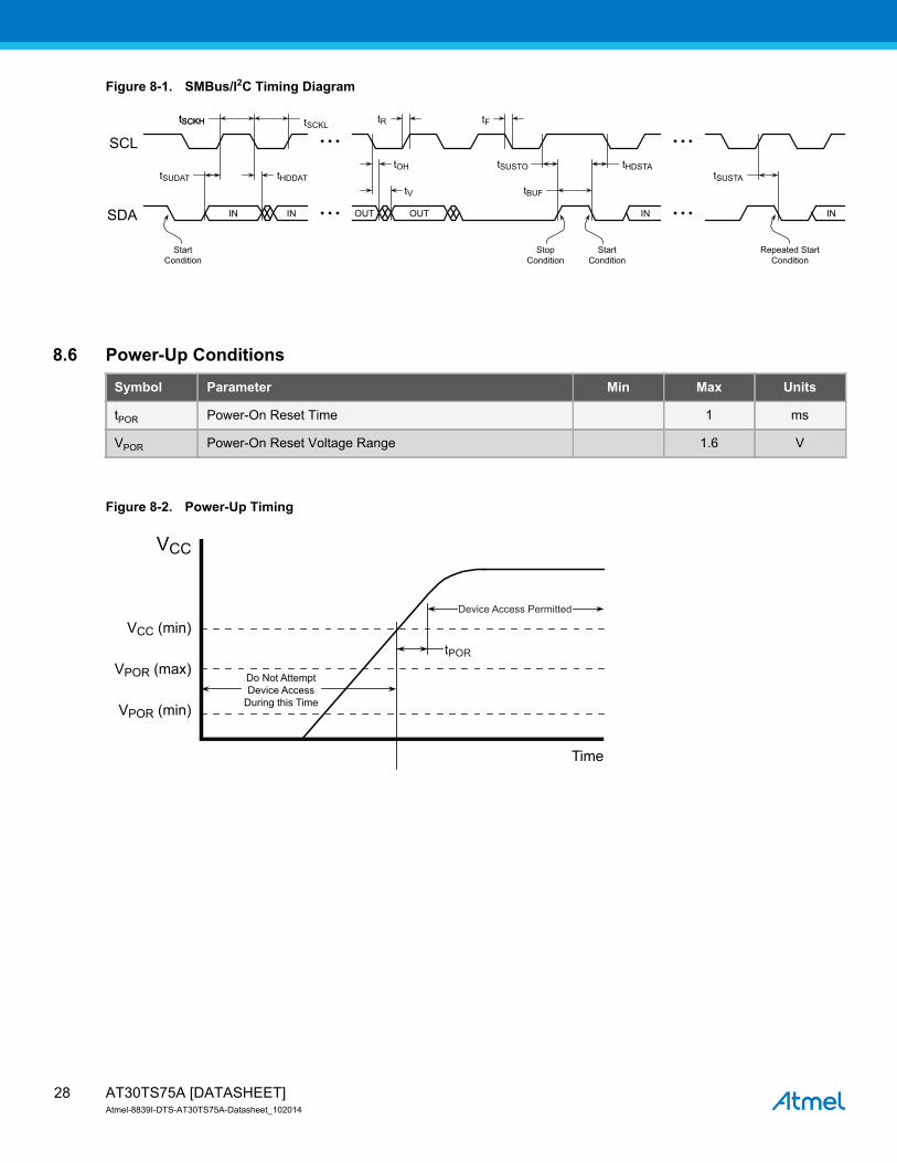
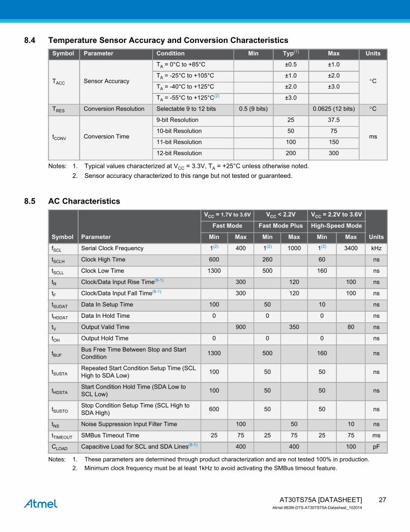
Figure 8-1. SMBus/I2C Timing Diagram
8.6 Power-Up Conditions
Figure 8-2. Power-Up Timing
SCL
SDA
StartCondition
StopCondition
Repeated StartCondition
StartCondition
tSCKHtSCKH
tSUDAT
tSCKL
tHDDATtOH
tR tF
tSUSTO
tV tBUF
tHDSTAtSUSTA
IN IN OUT OUT IN IN
Symbol Parameter Min Max Units
tPOR Power-On Reset Time 1 ms
VPOR Power-On Reset Voltage Range 1.6 V
VCC
VCC (min)
VPOR (max)
VPOR (min)
Time
Do Not AttemptDevice Access
During this Time
Device Access Permitted
tPOR
AT30TS75A [DATASHEET]Atmel-8839I-DTS-AT30TS75A-Datasheet_102014
28
8.7 Pin Capacitance
Note: 1. Not 100% tested (value guaranteed by design and characterization).
8.8 Input Test Waveforms and Measurement Levels
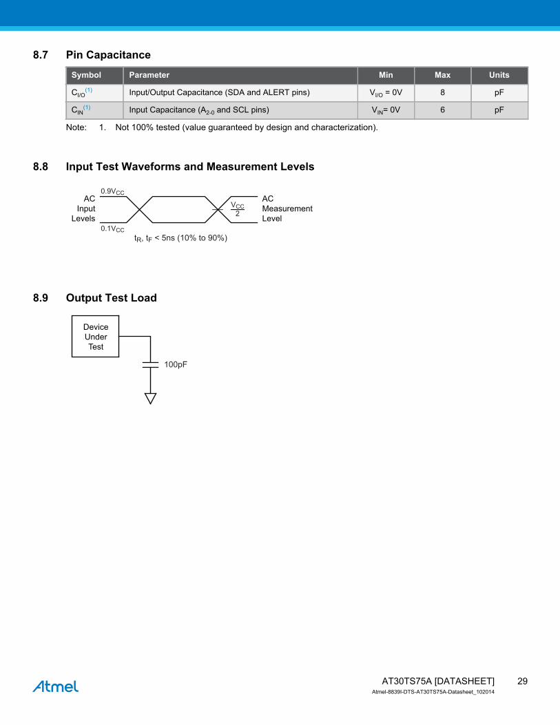
8.9 Output Test Load
Symbol Parameter Min Max Units
CI/O(1) Input/Output Capacitance (SDA and ALERT pins) VI/O = 0V 8 pF
CIN(1) Input Capacitance (A2-0 and SCL pins) VIN= 0V 6 pF
ACInput
Levels
AC MeasurementLevel
tR, tF < 5ns (10% to 90%)
0.9VCC
0.1VCC
VCC2
DeviceUnderTest
100pF
29AT30TS75A [DATASHEET]Atmel-8839I-DTS-AT30TS75A-Datasheet_102014
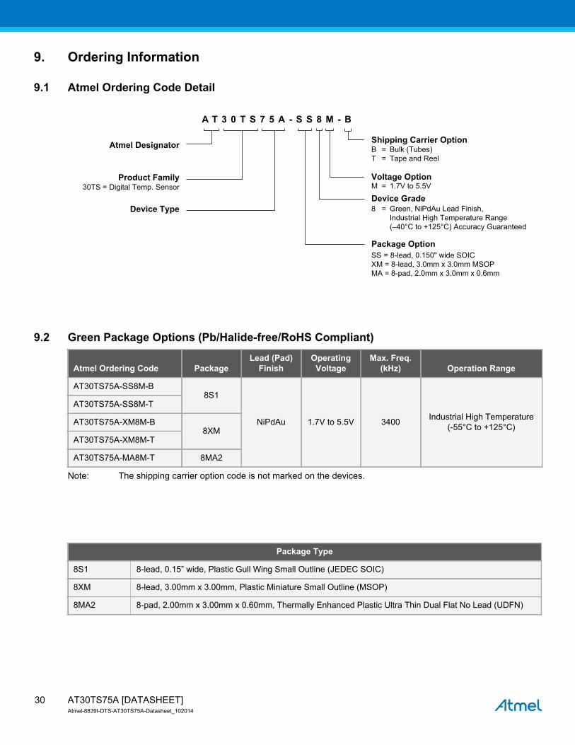
9. Ordering Information
9.1 Atmel Ordering Code Detail
9.2 Green Package Options (Pb/Halide-free/RoHS Compliant)
Note: The shipping carrier option code is not marked on the devices.
A T 3 0 T S 7 5 A - S S 8 M - B
Atmel Designator
Product Family
Device Type
Shipping Carrier Option
Device Grade
Voltage Option
Package Option
30TS = Digital Temp. Sensor
B = Bulk (Tubes)T = Tape and Reel
M = 1.7V to 5.5V
8 = Green, NiPdAu Lead Finish, Industrial High Temperature Range (–40°C to +125°C) Accuracy Guaranteed
SS = 8-lead, 0.150" wide SOICXM = 8-lead, 3.0mm x 3.0mm MSOPMA = 8-pad, 2.0mm x 3.0mm x 0.6mm
Atmel Ordering Code Package
Lead (Pad)
Finish
Operating
Voltage
Max. Freq.
(kHz) Operation Range
AT30TS75A-SS8M-B8S1
NiPdAu 1.7V to 5.5V 3400Industrial High Temperature
(-55°C to +125°C)
AT30TS75A-SS8M-T
AT30TS75A-XM8M-B8XM
AT30TS75A-XM8M-T
AT30TS75A-MA8M-T 8MA2
Package Type
8S1 8-lead, 0.15” wide, Plastic Gull Wing Small Outline (JEDEC SOIC)
8XM 8-lead, 3.00mm x 3.00mm, Plastic Miniature Small Outline (MSOP)
8MA2 8-pad, 2.00mm x 3.00mm x 0.60mm, Thermally Enhanced Plastic Ultra Thin Dual Flat No Lead (UDFN)
AT30TS75A [DATASHEET]Atmel-8839I-DTS-AT30TS75A-Datasheet_102014
30
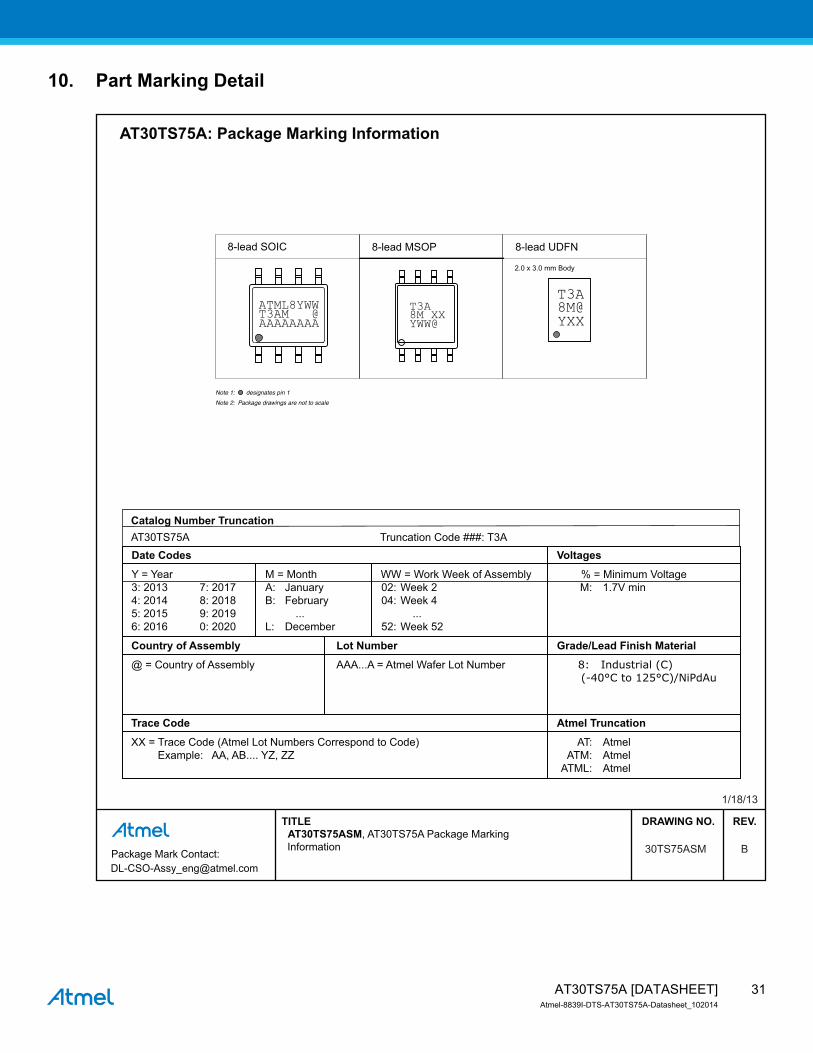
10. Part Marking Detail
DRAWING NO. REV. TITLE
30TS75ASM B
1/18/13
AT30TS75ASM, AT30TS75A Package Marking Information
Package Mark Contact:[email protected]
AAAAAAAAT3AM @ATML8YWW
8-lead SOIC 8-lead UDFN
T3A8M@YXX
2.0 x 3.0 mm Body
Note 2: Package drawings are not to scale
Note 1: designates pin 1
AT30TS75A: Package Marking Information
Catalog Number Truncation AT30TS75A Truncation Code ###: T3ADate Codes Voltages
Y = Year M = Month WW = Work Week of Assembly % = Minimum Voltage 3: 2013 7: 2017 A: January 02: Week 2 M: 1.7V min4: 2014 8: 2018 B: February 04: Week 4 5: 2015 9: 2019 ... ... 6: 2016 0: 2020 L: December 52: Week 52
Country of Assembly Lot Number Grade/Lead Finish Material
@ = Country of Assembly AAA...A = Atmel Wafer Lot Number 8: Industrial (C) (-40°C to 125°C)/NiPdAu
Trace Code Atmel Truncation
XX = Trace Code (Atmel Lot Numbers Correspond to Code) AT: Atmel Example: AA, AB.... YZ, ZZ ATM: Atmel ATML: Atmel
YWW@8M XXT3A
8-lead MSOP
31AT30TS75A [DATASHEET]Atmel-8839I-DTS-AT30TS75A-Datasheet_102014
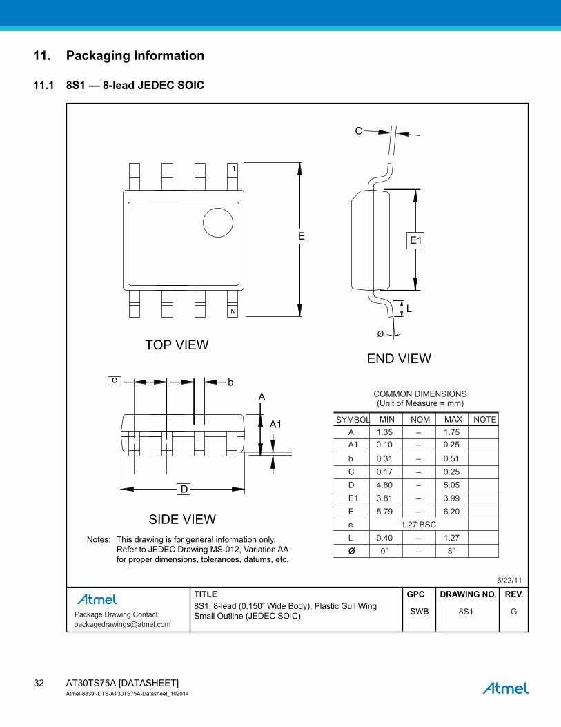
11. Packaging Information
11.1 8S1 — 8-lead JEDEC SOIC
DRAWING NO. REV. TITLE GPC
COMMON DIMENSIONS(Unit of Measure = mm)
SYMBOL MIN NOM MAX NOTE
A1 0.10 – 0.25 A 1.35 – 1.75
b 0.31 – 0.51 C 0.17 – 0.25 D 4.80 – 5.05 E1 3.81 – 3.99 E 5.79 – 6.20 e 1.27 BSC L 0.40 – 1.27 ØØ 0° – 8°
Ø
E
1
N
TOP VIEW
C
E1
END VIEW
Ab
L
A1
e
D
SIDE VIEW
Package Drawing Contact:[email protected]
8S1 G
6/22/11
Notes: This drawing is for general information only. Refer to JEDEC Drawing MS-012, Variation AA for proper dimensions, tolerances, datums, etc.
8S1, 8-lead (0.150” Wide Body), Plastic Gull Wing Small Outline (JEDEC SOIC) SWB
AT30TS75A [DATASHEET]Atmel-8839I-DTS-AT30TS75A-Datasheet_102014
32
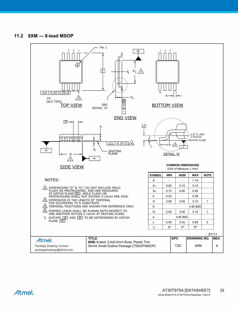
11.2 8XM — 8-lead MSOP
TITLE DRAWING NO. GPC REV.
Package Drawing Contact:[email protected]
8XMTZD A8XM, 8-lead, 3.0x3.0mm Body, Plastic ThinShrink Small Outline Package (TSSOP/MSOP)
3/1/11
COMMON DIMENSIONS(Unit of Measure = mm)
SYMBOL MIN NOM MAX NOTE
A - - 1.10
A1 0.05 0.10 0.15
A2 0.75 0.85 0.95
b 0.22 - 0.38
D 2.90 3.00 3.10 1
E 4.90 BSC
E1 2.90 3.00 3.10 1
e 0.65 BSC
L 0.40 0.55 0.80 2
A
e
OCC
A1
N
Pin 1
E
1
1
A23
SIDE VIEW
END VIEW
DETAIL 'A'
TOP VIEW
SEATINGPLANE
123
SEEDETAIL "A"
2L4
1.
ONE ANOTHER WITHIN 0.10mm AT SEATING PLANE.4.
3.
2.
FORMED LEADS SHALL BE PLANAR WITH RESPECT TO
TERMINAL POSITIONS ARE SHOWN FOR REFERENCE ONLY.FOR SOLDERING TO A SUBSTRATE.DIMENSION IS THE LENGTH OF TERMINALPROTRUSIONS SHALL NOT EXCEED 0.15mm PER SIDE.AT DATUM PLANE -H- , MOLD FLASH ORFLASH OR PROTRUSIONS, AND ARE MEASUREDDIMENSIONS "D" & "E1" DO NOT INCLUDE MOLD
NOTES:
C0.10
CL
BSC0.25
D
C0.20 B A
2X(N/2 TIPS)
E1
0.07 R. MIN2 PLACES
-C-
SEATING PLANE
-H-
-A-
-B-
S0.0
5
5. DATUMS -A- AND -B- TO BE DETERMINED BY DATUMPLANE -H- .
BOTTOM VIEW
N
321
8°0°CCO 4°
b
33AT30TS75A [DATASHEET]Atmel-8839I-DTS-AT30TS75A-Datasheet_102014
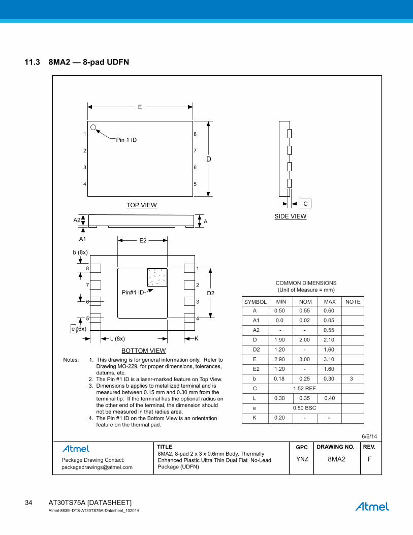
11.3 8MA2 — 8-pad UDFN
DRAWING NO. REV. TITLE GPC
8MA2 F
6/6/14
8MA2, 8-pad 2 x 3 x 0.6mm Body, ThermallyEnhanced Plastic Ultra Thin Dual Flat No-LeadPackage (UDFN)
YNZ
COMMON DIMENSIONS(Unit of Measure = mm)
SYMBOL MIN NOM MAX NOTE A 0.50 0.55 0.60
A1 0.0 0.02 0.05
A2 - - 0.55
D 1.90 2.00 2.10
D2 1.20 - 1.60
E 2.90 3.00 3.10
E2 1.20 - 1.60
b 0.18 0.25 0.30 3
C 1.52 REF
L 0.30 0.35 0.40
e 0.50 BSC
K 0.20 - -
TOP VIEW
SIDE VIEW
BOTTOM VIEW
Package Drawing Contact:[email protected]
C
E
Pin 1 ID
D
8
7
6
5
1
2
3
4
A
A1
A2
D2
E2
e (6x)
L (8x)
b (8x)
Pin#1 ID
K
1
2
3
4
8
7
6
5
Notes: 1. This drawing is for general information only. Refer to Drawing MO-229, for proper dimensions, tolerances, datums, etc. 2. The Pin #1 ID is a laser-marked feature on Top View. 3. Dimensions b applies to metallized terminal and is measured between 0.15 mm and 0.30 mm from the terminal tip. If the terminal has the optional radius on the other end of the terminal, the dimension should not be measured in that radius area. 4. The Pin #1 ID on the Bottom View is an orientation feature on the thermal pad.
AT30TS75A [DATASHEET]Atmel-8839I-DTS-AT30TS75A-Datasheet_102014
34
12. Errata
12.1 ALERT Pin State
Issue: When switching between Comparator and Interrupt modes (or vice versa) while the ALERT
pin is active, the device will not retain its active alert state and will automatically deassert
the ALERT pin.
Workaround: None.
Resolution: The operation of the ALERT pin will be changed with a new revision of the AT30TS75A device so
it will properly retain the ALERT pin status when switching modes. Please contact Atmel for the
estimated availability of the new revision and the method for distinguishing between device
versions.
35AT30TS75A [DATASHEET]Atmel-8839I-DTS-AT30TS75A-Datasheet_102014
13. Revision History
Doc. Rev. Date Comments
8839I 10/2014Update the DC Characteristics and the AC Characteristics tables and the UDFN-8MA2
package outline drawing.
8839H 04/2014 Add errata.
8839G 03/2014 Update values in the DC Characteristics table.
8839F 01/2014 Increase ICC1 typical from 75μA to 85μA and maximum from 100μA to 125μA.
8839E 10/2013 Update a few minor typos in various sections.
8839D 09/2013Update Absolute Maximum Rating section.
Update values in the AC Characteristics table.
8839C 07/2013 Update from preliminary to complete/release status.
8839B 05/2013
Update disclaimer page.
Update Tables 8-3 and 8-7.
Update 8MA2 package drawing.
8839A 02/2013 Initial document release.
AT30TS75A [DATASHEET]Atmel-8839I-DTS-AT30TS75A-Datasheet_102014
36
XX X XX X
Atmel Corporation 1600 Technology Drive, San Jose, CA 95110 USA T: (+1)(408) 441.0311 F: (+1)(408) 436.4200 | www.atmel.com
© 2014 Atmel Corporation. / Rev.: Atmel-8855F-DTS-AT30TS750A-Datasheet_102014.
Atmel®, Atmel logo and combinations thereof, Enabling Unlimited Possibilities®, and others are registered trademarks or trademarks of Atmel Corporation in U.S. and other countries. Other terms and product names may be trademarks of others.
DISCLAIMER: The information in this document is provided in connection with Atmel products. No license, express or implied, by estoppel or otherwise, to any intellectual property rightis granted by this document or in connection with the sale of Atmel products. EXCEPT AS SET FORTH IN THE ATMEL TERMS AND CONDITIONS OF SALES LOCATED ON THEATMEL WEBSITE, ATMEL ASSUMES NO LIABILITY WHATSOEVER AND DISCLAIMS ANY EXPRESS, IMPLIED OR STATUTORY WARRANTY RELATING TO ITS PRODUCTSINCLUDING, BUT NOT LIMITED TO, THE IMPLIED WARRANTY OF MERCHANTABILITY, FITNESS FOR A PARTICULAR PURPOSE, OR NON-INFRINGEMENT. IN NO EVENTSHALL ATMEL BE LIABLE FOR ANY DIRECT, INDIRECT, CONSEQUENTIAL, PUNITIVE, SPECIAL OR INCIDENTAL DAMAGES (INCLUDING, WITHOUT LIMITATION, DAMAGESFOR LOSS AND PROFITS, BUSINESS INTERRUPTION, OR LOSS OF INFORMATION) ARISING OUT OF THE USE OR INABILITY TO USE THIS DOCUMENT, EVEN IF ATMEL HASBEEN ADVISED OF THE POSSIBILITY OF SUCH DAMAGES. Atmel makes no representations or warranties with respect to the accuracy or completeness of the contents of thisdocument and reserves the right to make changes to specifications and products descriptions at any time without notice. Atmel does not make any commitment to update the informationcontained herein. Unless specifically provided otherwise, Atmel products are not suitable for, and shall not be used in, automotive applications. Atmel products are not intended,authorized, or warranted for use as components in applications intended to support or sustain life.
SAFETY-CRITICAL, MILITARY, AND AUTOMOTIVE APPLICATIONS DISCLAIMER: Atmel products are not designed for and will not be used in connection with any applications wherethe failure of such products would reasonably be expected to result in significant personal injury or death (“Safety-Critical Applications”) without an Atmel officer's specific writtenconsent. Safety-Critical Applications include, without limitation, life support devices and systems, equipment or systems for the operation of nuclear facilities and weapons systems.Atmel products are not designed nor intended for use in military or aerospace applications or environments unless specifically designated by Atmel as military-grade. Atmel products arenot designed nor intended for use in automotive applications unless specifically designated by Atmel as automotive-grade.