Embed Size (px)
Citation preview
AT91 ARM Thumb-based Microcontrollers
Application Note
6327B–ATARM–22-Aug-07
AT91-AN01: Using the Two-wire interface (TWI) in Master Mode on AT91SAM Microcontrollers
1. Scope The purpose of this document is to help the hardware and software developer in thedesign of a system using the Two-wire Interface (TWI) embedded in the AT91SAMproduct family of ARM® Thumb®-based microcontrollers with Atmel's Two-wire Inter-face slave devices and I²C-Bus compatible slave devices. It describes the connectionwith a digital temperature sensor, a Real Time Clock (RTC), a Graphic LCD Module(GLCD) and a 1Mbit Two-wire Serial EEPROM. In this TWI/I²C-compatible network,only one Master is present, the AT91SAM device, and all other devices are slavedevices. This application note also provides a demonstration software project whichdisplays static and animated images, temperature, time and date.
The board used in this application note is the AT91SAM7S256-EK.
• I²C Temperature Sensor: LM75 (National Semiconductor®).
• I²C Real Time Clock: DS1337 (Maxim-Dallas).
• TWI Serial EEPROM: AT24C1024 (Atmel).
• I²C Graphic LCD: Chip-On-Glass (COG) 96 x 40 Dot Matrix LCD module (Batron with NXP PCF8558 LCD controller)
The associated zip file, AN-AT91SAM-TWI-software.zip, contains the source codeexample described in Section 6.4 “Associated Source Code Example and Projects” onpage 26.
2. Associated DocumentationBefore going further into this document, refer to the latest documents for the corre-sponding AT91SAM (AT91SAM7 or AT91SAM9) device on the Atmel Web site.http://www.atmel.com/products/AT91/
3. Terminology, Abbreviations and Typographical Conventions
4. Two-wire Interface OverviewThe Two-wire Interface (TWI) interconnects components on a unique two-wire bus, made up ofone clock line and one data line with speeds of up to 400 Kbits per second, based on a byte-ori-ented transfer format. It can be used with any Atmel Two-wire Interface bus Serial EEPROM andI²C compatible device such as Real Time Clock (RTC), Dot Matrix/Graphic LCD Controllers andTemperature Sensor, to name but a few. The TWI is programmable as master transmitter ormaster receiver with sequential or single-byte access. A configurable baud rate generator per-mits the output data rate to be adapted to a wide range of core clock frequencies. Below, Table4-1 lists the compatibility level of the Atmel Two-wire Interface and a full I²C compatible device.
Notes: 1. START + b000000001 + Ack + Sr
2. A repeated start condition is only supported in Master Receiver mode.
Abbreviation Description
TWI Two-wire Interface
A Acknowledge
NA Non Acknowledge
P Stop
S Start
Sr Repeated Start
SADR Slave Address
ADR Any address except SADR
R Read
W Write
Table 4-1. Atmel TWI Compatibility with I²C Standard
I²C Standard Atmel TWI
Standard Mode Speed (100 KHz) Supported
Fast Mode Speed (400 KHz) Supported
7 or 10 bits Slave Addressing Supported
START BYTE(1) Not Supported
Repeated Start (Sr) Condition Not Fully Supported(2)
ACK and NACK Management Supported
Slope control and input filtering (Fast mode) Not Supported
Clock stretching Supported
26327B–ATARM–22-Aug-07
Application Note
Application Note
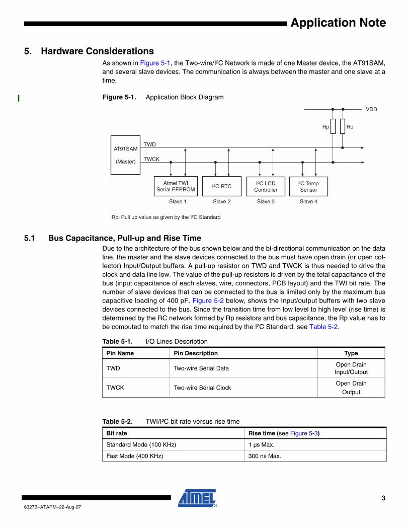
5. Hardware ConsiderationsAs shown in Figure 5-1, the Two-wire/I²C Network is made of one Master device, the AT91SAM,and several slave devices. The communication is always between the master and one slave at atime.
Figure 5-1. Application Block Diagram
5.1 Bus Capacitance, Pull-up and Rise TimeDue to the architecture of the bus shown below and the bi-directional communication on the dataline, the master and the slave devices connected to the bus must have open drain (or open col-lector) Input/Output buffers. A pull-up resistor on TWD and TWCK is thus needed to drive theclock and data line low. The value of the pull-up resistors is driven by the total capacitance of thebus (input capacitance of each slaves, wire, connectors, PCB layout) and the TWI bit rate. Thenumber of slave devices that can be connected to the bus is limited only by the maximum buscapacitive loading of 400 pF. Figure 5-2 below, shows the Input/output buffers with two slavedevices connected to the bus. Since the transition time from low level to high level (rise time) isdetermined by the RC network formed by Rp resistors and bus capacitance, the Rp value has tobe computed to match the rise time required by the I²C Standard, see Table 5-2.
AT91SAM
(Master)
TWD
TWCK
Atmel TWISerial EEPROM
I²C RTC I²C LCDController
Slave 1 Slave 2 Slave 3
VDD
I²C Temp.Sensor
Slave 4
Rp: Pull up value as given by the I²C Standard
Rp Rp
Table 5-1. I/O Lines Description
Pin Name Pin Description Type
TWD Two-wire Serial DataOpen Drain Input/Output
TWCK Two-wire Serial ClockOpen Drain
Output
Table 5-2. TWI/I²C bit rate versus rise time
Bit rate Rise time (see Figure 5-3)
Standard Mode (100 KHz) 1 µs Max.
Fast Mode (400 KHz) 300 ns Max.
36327B–ATARM–22-Aug-07
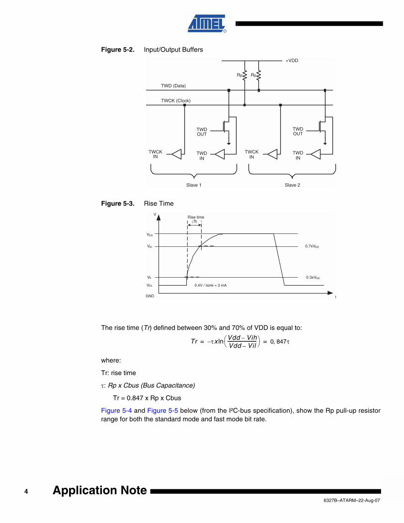
Figure 5-2. Input/Output Buffers
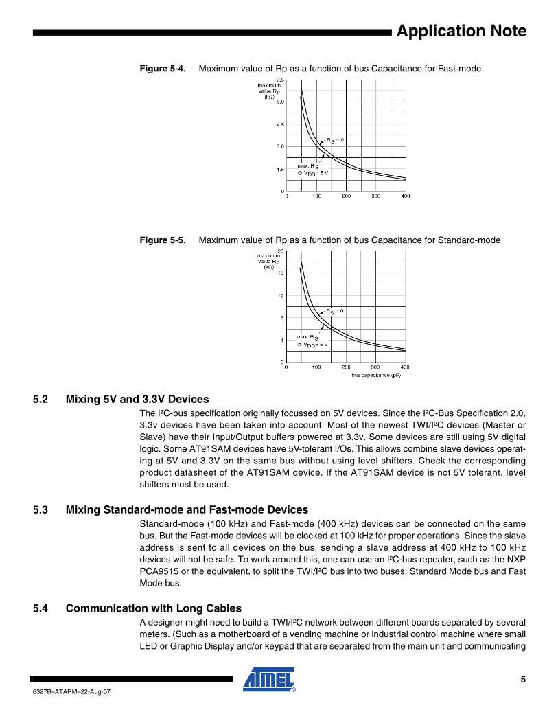
Figure 5-3. Rise Time
The rise time (Tr) defined between 30% and 70% of VDD is equal to:
where:
Tr: rise time
τ: Rp x Cbus (Bus Capacitance)
Tr = 0.847 x Rp x Cbus
Figure 5-4 and Figure 5-5 below (from the I²C-bus specification), show the Rp pull-up resistorrange for both the standard mode and fast mode bit rate.
Rp Rp
+VDD
TWD (Data)
TWCK (Clock)
TWCKIN
TWDOUT
TWDIN
TWDOUT
TWDIN
Slave 1 Slave 2
TWCKIN
VOL
VIH
VIL
VDD
0.3xVDD
0.7xVDD
GND
0.4V / Isink = 3 mA
Rise time(Tr)
V
t
Tr τx Vdd Vih–Vdd Vil–--------------------------⎝ ⎠⎛ ⎞ln– 0 847τ,= =
46327B–ATARM–22-Aug-07
Application Note
Application Note
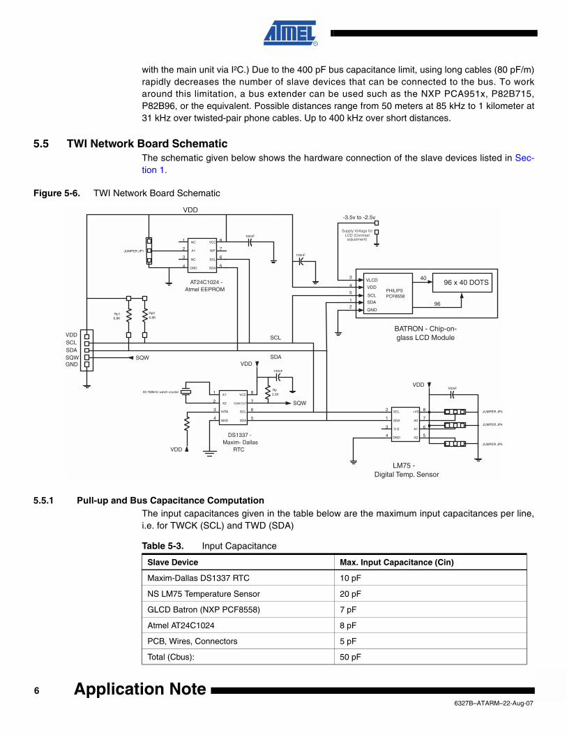
Figure 5-4. Maximum value of Rp as a function of bus Capacitance for Fast-mode
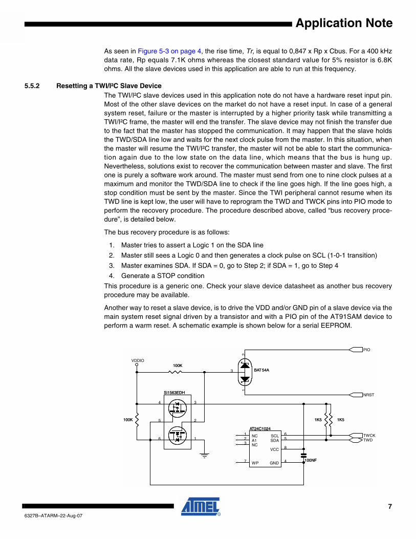
Figure 5-5. Maximum value of Rp as a function of bus Capacitance for Standard-mode
5.2 Mixing 5V and 3.3V DevicesThe I²C-bus specification originally focussed on 5V devices. Since the I²C-Bus Specification 2.0,3.3v devices have been taken into account. Most of the newest TWI/I²C devices (Master orSlave) have their Input/Output buffers powered at 3.3v. Some devices are still using 5V digitallogic. Some AT91SAM devices have 5V-tolerant I/Os. This allows combine slave devices operat-ing at 5V and 3.3V on the same bus without using level shifters. Check the correspondingproduct datasheet of the AT91SAM device. If the AT91SAM device is not 5V tolerant, levelshifters must be used.
5.3 Mixing Standard-mode and Fast-mode DevicesStandard-mode (100 kHz) and Fast-mode (400 kHz) devices can be connected on the samebus. But the Fast-mode devices will be clocked at 100 kHz for proper operations. Since the slaveaddress is sent to all devices on the bus, sending a slave address at 400 kHz to 100 kHzdevices will not be safe. To work around this, one can use an I²C-bus repeater, such as the NXPPCA9515 or the equivalent, to split the TWI/I²C bus into two buses; Standard Mode bus and FastMode bus.
5.4 Communication with Long CablesA designer might need to build a TWI/I²C network between different boards separated by severalmeters. (Such as a motherboard of a vending machine or industrial control machine where smallLED or Graphic Display and/or keypad that are separated from the main unit and communicating
56327B–ATARM–22-Aug-07
with the main unit via I²C.) Due to the 400 pF bus capacitance limit, using long cables (80 pF/m)rapidly decreases the number of slave devices that can be connected to the bus. To workaround this limitation, a bus extender can be used such as the NXP PCA951x, P82B715,P82B96, or the equivalent. Possible distances range from 50 meters at 85 kHz to 1 kilometer at31 kHz over twisted-pair phone cables. Up to 400 kHz over short distances.
5.5 TWI Network Board SchematicThe schematic given below shows the hardware connection of the slave devices listed in Sec-tion 1.
Figure 5-6. TWI Network Board Schematic
5.5.1 Pull-up and Bus Capacitance ComputationThe input capacitances given in the table below are the maximum input capacitances per line,i.e. for TWCK (SCL) and TWD (SDA)
Rp16.8K
100nF32,768kHz watch crystal
DS1337 -Maxim- Dallas
RTC
LM75 -Digital Temp. Sensor
100nF
Rp2 6.8K
100nF
1
2
3
4
8
7
6
5
X1
SDA
SCL
SQW/OUT
VCC
GND
INTA
X2
AT24C1024 -Atmel EEPROM
1
2
3
4
8
7
6
5
NC
SDA
SCL
WP
VCC
GND
NC
A1
SDA
SCL
SDASCLVDD
GND
1
2
3
4
8
7
6
5
SCL
A2
A1
A0
+VS
GND
O.S
SDA
96 x 40 DOTSPHILIPSPCF8558
40
96
VDD
VLCD
GND
SCL
SDA
3
4
2
5
1
VDD
100nF
VDD
VDD
Rp 2.2K
VDD
JUMPER JP1
JUMPER JP3
JUMPER JP4
JUMPER JP5
BATRON - Chip-on-glass LCD Module
Supply Voltage forLCD (Contrastadjustment)
-3.5v to -2.5v
SQW SQW
SQW
Table 5-3. Input Capacitance
Slave Device Max. Input Capacitance (Cin)
Maxim-Dallas DS1337 RTC 10 pF
NS LM75 Temperature Sensor 20 pF
GLCD Batron (NXP PCF8558) 7 pF
Atmel AT24C1024 8 pF
PCB, Wires, Connectors 5 pF
Total (Cbus): 50 pF
66327B–ATARM–22-Aug-07
Application Note
Application Note
As seen in Figure 5-3 on page 4, the rise time, Tr, is equal to 0,847 x Rp x Cbus. For a 400 kHzdata rate, Rp equals 7.1K ohms whereas the closest standard value for 5% resistor is 6.8Kohms. All the slave devices used in this application are able to run at this frequency.
5.5.2 Resetting a TWI/I²C Slave DeviceThe TWI/I²C slave devices used in this application note do not have a hardware reset input pin.Most of the other slave devices on the market do not have a reset input. In case of a generalsystem reset, failure or the master is interrupted by a higher priority task while transmitting aTWI/I²C frame, the master will end the transfer. The slave device may not finish the transfer dueto the fact that the master has stopped the communication. It may happen that the slave holdsthe TWD/SDA line low and waits for the next clock pulse from the master. In this situation, whenthe master will resume the TWI/I²C transfer, the master will not be able to start the communica-tion again due to the low state on the data line, which means that the bus is hung up.Nevertheless, solutions exist to recover the communication between master and slave. The firstone is purely a software work around. The master must send from one to nine clock pulses at amaximum and monitor the TWD/SDA line to check if the line goes high. If the line goes high, astop condition must be sent by the master. Since the TWI peripheral cannot resume when itsTWD line is kept low, the user will have to reprogram the TWD and TWCK pins into PIO mode toperform the recovery procedure. The procedure described above, called “bus recovery proce-dure”, is detailed below.
The bus recovery procedure is as follows:
1. Master tries to assert a Logic 1 on the SDA line
2. Master still sees a Logic 0 and then generates a clock pulse on SCL (1-0-1 transition)
3. Master examines SDA. If SDA = 0, go to Step 2; if SDA = 1, go to Step 4
4. Generate a STOP condition
This procedure is a generic one. Check your slave device datasheet as another bus recoveryprocedure may be available.
Another way to reset a slave device, is to drive the VDD and/or GND pin of a slave device via themain system reset signal driven by a transistor and with a PIO pin of the AT91SAM device toperform a warm reset. A schematic example is shown below for a serial EEPROM.
TWCKTWD
PIO
NRST
VDDIO100K100K
Si1563EDHSi1563EDH
1
3
2
4
5
6
100K100K 1K51K5 1K51K5
AT24C1024AT24C10241 NC
A12
WP7
SCL 6
VCC 8NC3
SDA 5
GND 4
BAT54ABAT54A
1
3
2
100NF100NF
76327B–ATARM–22-Aug-07
6. Software and Application ConsiderationsThe Transfer Format and Modes of Operation sections below give a brief reminder of the TWIoperation. For further details and register definitions refer to the corresponding AT91SAM7 orAT91SAM9 datasheet.
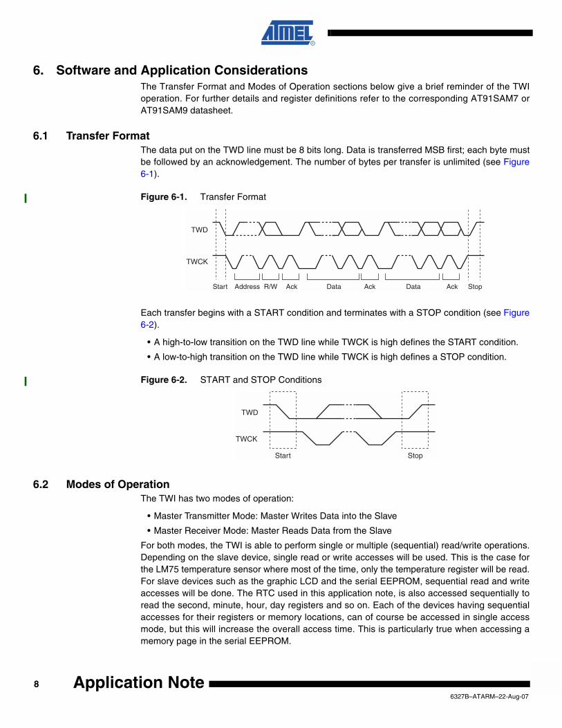
6.1 Transfer FormatThe data put on the TWD line must be 8 bits long. Data is transferred MSB first; each byte mustbe followed by an acknowledgement. The number of bytes per transfer is unlimited (see Figure6-1).
Figure 6-1. Transfer Format
Each transfer begins with a START condition and terminates with a STOP condition (see Figure6-2).
• A high-to-low transition on the TWD line while TWCK is high defines the START condition.
• A low-to-high transition on the TWD line while TWCK is high defines a STOP condition.
Figure 6-2. START and STOP Conditions
6.2 Modes of OperationThe TWI has two modes of operation:
• Master Transmitter Mode: Master Writes Data into the Slave
• Master Receiver Mode: Master Reads Data from the Slave
For both modes, the TWI is able to perform single or multiple (sequential) read/write operations.Depending on the slave device, single read or write accesses will be used. This is the case forthe LM75 temperature sensor where most of the time, only the temperature register will be read.For slave devices such as the graphic LCD and the serial EEPROM, sequential read and writeaccesses will be done. The RTC used in this application note, is also accessed sequentially toread the second, minute, hour, day registers and so on. Each of the devices having sequentialaccesses for their registers or memory locations, can of course be accessed in single accessmode, but this will increase the overall access time. This is particularly true when accessing amemory page in the serial EEPROM.
TWD
TWCK
Start Address R/W Ack Data Ack Data Ack Stop
TWD
TWCK
Start Stop
86327B–ATARM–22-Aug-07
Application Note
Application Note
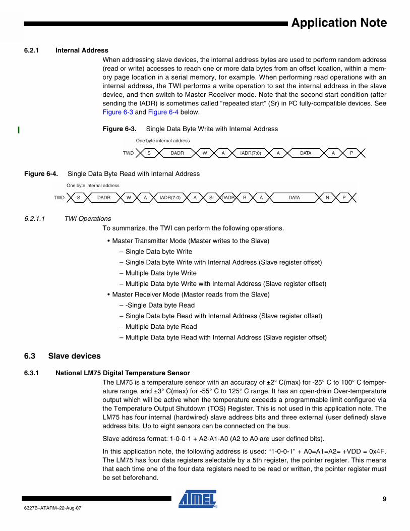
6.2.1 Internal AddressWhen addressing slave devices, the internal address bytes are used to perform random address(read or write) accesses to reach one or more data bytes from an offset location, within a mem-ory page location in a serial memory, for example. When performing read operations with aninternal address, the TWI performs a write operation to set the internal address in the slavedevice, and then switch to Master Receiver mode. Note that the second start condition (aftersending the IADR) is sometimes called “repeated start” (Sr) in I²C fully-compatible devices. SeeFigure 6-3 and Figure 6-4 below.
Figure 6-3. Single Data Byte Write with Internal Address
Figure 6-4. Single Data Byte Read with Internal Address
6.2.1.1 TWI OperationsTo summarize, the TWI can perform the following operations.
• Master Transmitter Mode (Master writes to the Slave)
– Single Data byte Write
– Single Data byte Write with Internal Address (Slave register offset)
– Multiple Data byte Write
– Multiple Data byte Write with Internal Address (Slave register offset)
• Master Receiver Mode (Master reads from the Slave)
– -Single Data byte Read
– Single Data byte Read with Internal Address (Slave register offset)
– Multiple Data byte Read
– Multiple Data byte Read with Internal Address (Slave register offset)
6.3 Slave devices
6.3.1 National LM75 Digital Temperature SensorThe LM75 is a temperature sensor with an accuracy of ±2° C(max) for -25° C to 100° C temper-ature range, and ±3° C(max) for -55° C to 125° C range. It has an open-drain Over-temperatureoutput which will be active when the temperature exceeds a programmable limit configured viathe Temperature Output Shutdown (TOS) Register. This is not used in this application note. TheLM75 has four internal (hardwired) slave address bits and three external (user defined) slaveaddress bits. Up to eight sensors can be connected on the bus.
Slave address format: 1-0-0-1 + A2-A1-A0 (A2 to A0 are user defined bits).
In this application note, the following address is used: “1-0-0-1” + A0=A1=A2= +VDD = 0x4F.The LM75 has four data registers selectable by a 5th register, the pointer register. This meansthat each time one of the four data registers need to be read or written, the pointer register mustbe set beforehand.
A IADR(7:0) A PDATA AS DADR W
One byte internal address
TWD
A IADR(7:0) AS DADR W Sr DADR R A DATA N PTWD
One byte internal address
96327B–ATARM–22-Aug-07
• Pointer Register: 8-bit (only 2 LSB’s are significant)
• Configuration Register: 8-bit
• Temperature Register: 16-bit (only 9 MSBs are significant)
• Temperature Output Shutdown Register: 16-bit (only 9 MSBs are significant)
• Temperature Hysteresis Register: 16-bit (only 9 MSBs are significant)
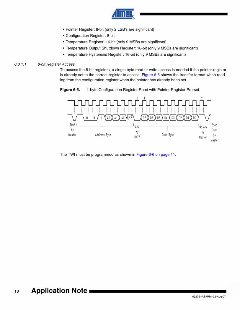
6.3.1.1 8-bit Register AccessTo access the 8-bit registers, a single byte read or write access is needed if the pointer registeris already set to the correct register to access. Figure 6-5 shows the transfer format when read-ing from the configuration register when the pointer has already been set.
Figure 6-5. 1-byte Configuration Register Read with Pointer Register Pre-set
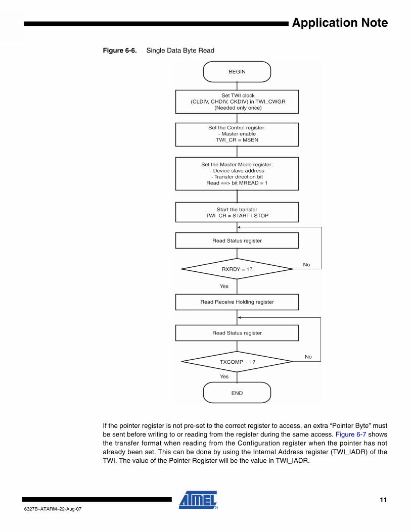
The TWI must be programmed as shown in Figure 6-6 on page 11.
106327B–ATARM–22-Aug-07
Application Note
Application Note
Figure 6-6. Single Data Byte Read
If the pointer register is not pre-set to the correct register to access, an extra “Pointer Byte” mustbe sent before writing to or reading from the register during the same access. Figure 6-7 showsthe transfer format when reading from the Configuration register when the pointer has notalready been set. This can be done by using the Internal Address register (TWI_IADR) of theTWI. The value of the Pointer Register will be the value in TWI_IADR.
Set the Control register:- Master enable
TWI_CR = MSEN
Set the Master Mode register:- Device slave address- Transfer direction bit
Read ==> bit MREAD = 1
Start the transferTWI_CR = START | STOP
Read Status register
RXRDY = 1?
Read Status register
TXCOMP = 1?
END
BEGIN
Yes
Yes
Set TWI clock(CLDIV, CHDIV, CKDIV) in TWI_CWGR
(Needed only once)
Read Receive Holding register
No
No
116327B–ATARM–22-Aug-07
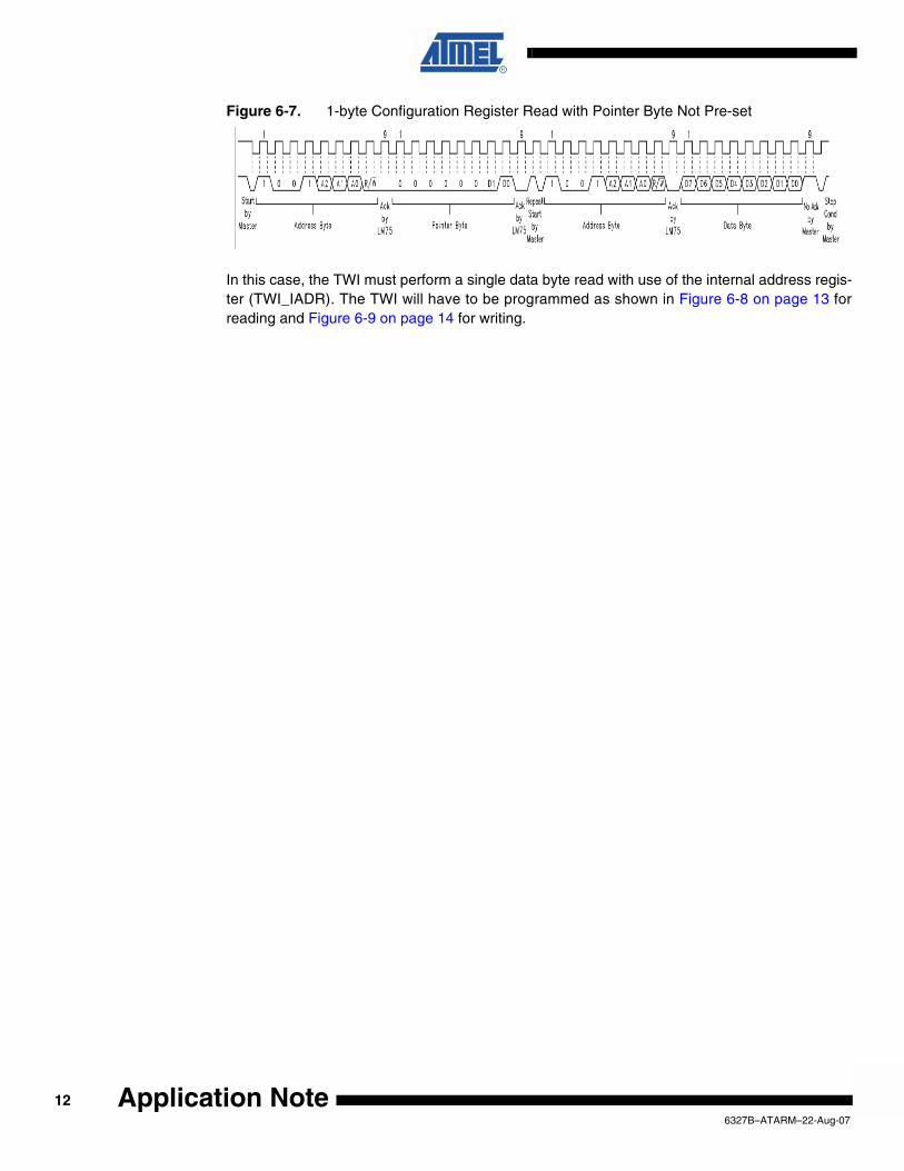
Figure 6-7. 1-byte Configuration Register Read with Pointer Byte Not Pre-set
In this case, the TWI must perform a single data byte read with use of the internal address regis-ter (TWI_IADR). The TWI will have to be programmed as shown in Figure 6-8 on page 13 forreading and Figure 6-9 on page 14 for writing.
126327B–ATARM–22-Aug-07
Application Note
Application Note
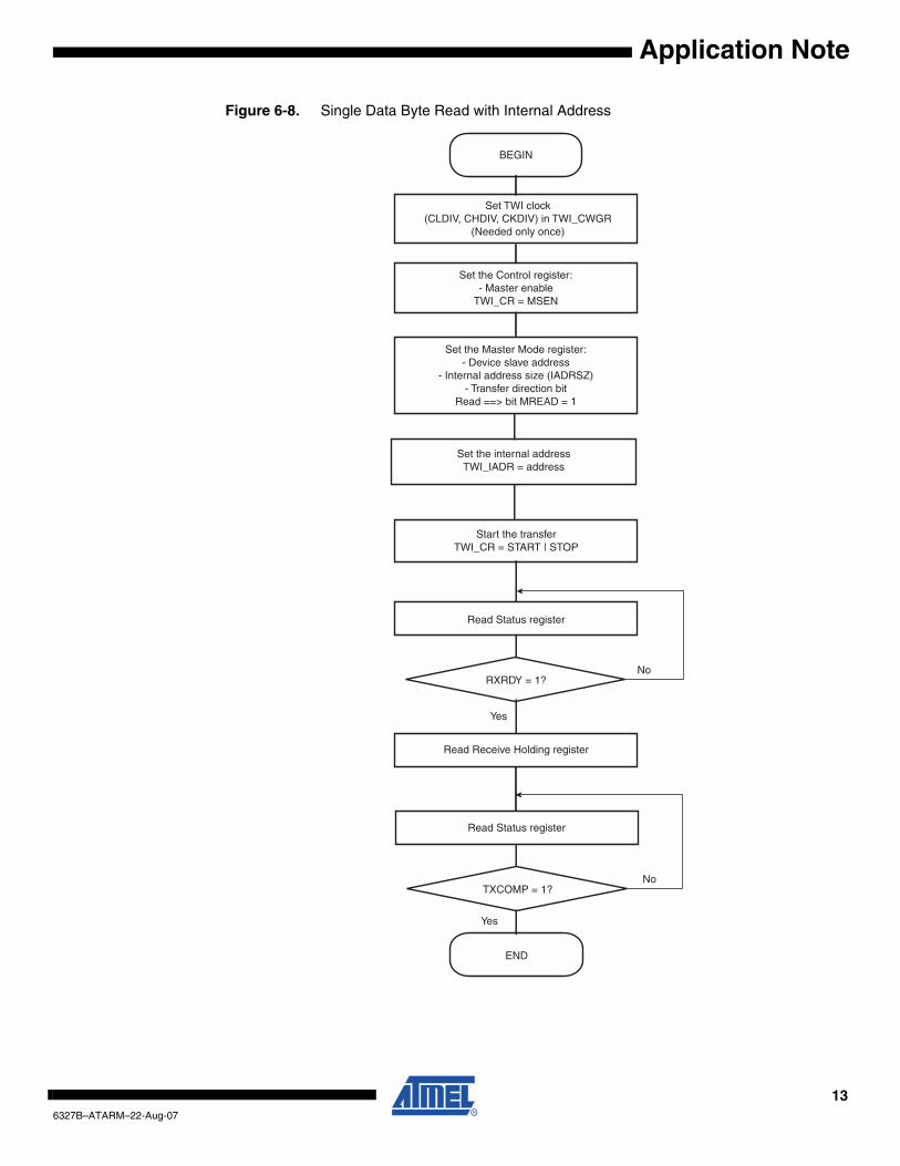
Figure 6-8. Single Data Byte Read with Internal Address
Set the Control register:- Master enable
TWI_CR = MSEN
Set the Master Mode register:- Device slave address
- Internal address size (IADRSZ)- Transfer direction bit
Read ==> bit MREAD = 1
Read Status register
TXCOMP = 1?
END
BEGIN
Yes
Set TWI clock(CLDIV, CHDIV, CKDIV) in TWI_CWGR
(Needed only once)
Yes
Set the internal addressTWI_IADR = address
Start the transferTWI_CR = START | STOP
Read Status register
RXRDY = 1?
Read Receive Holding register
No
No
136327B–ATARM–22-Aug-07
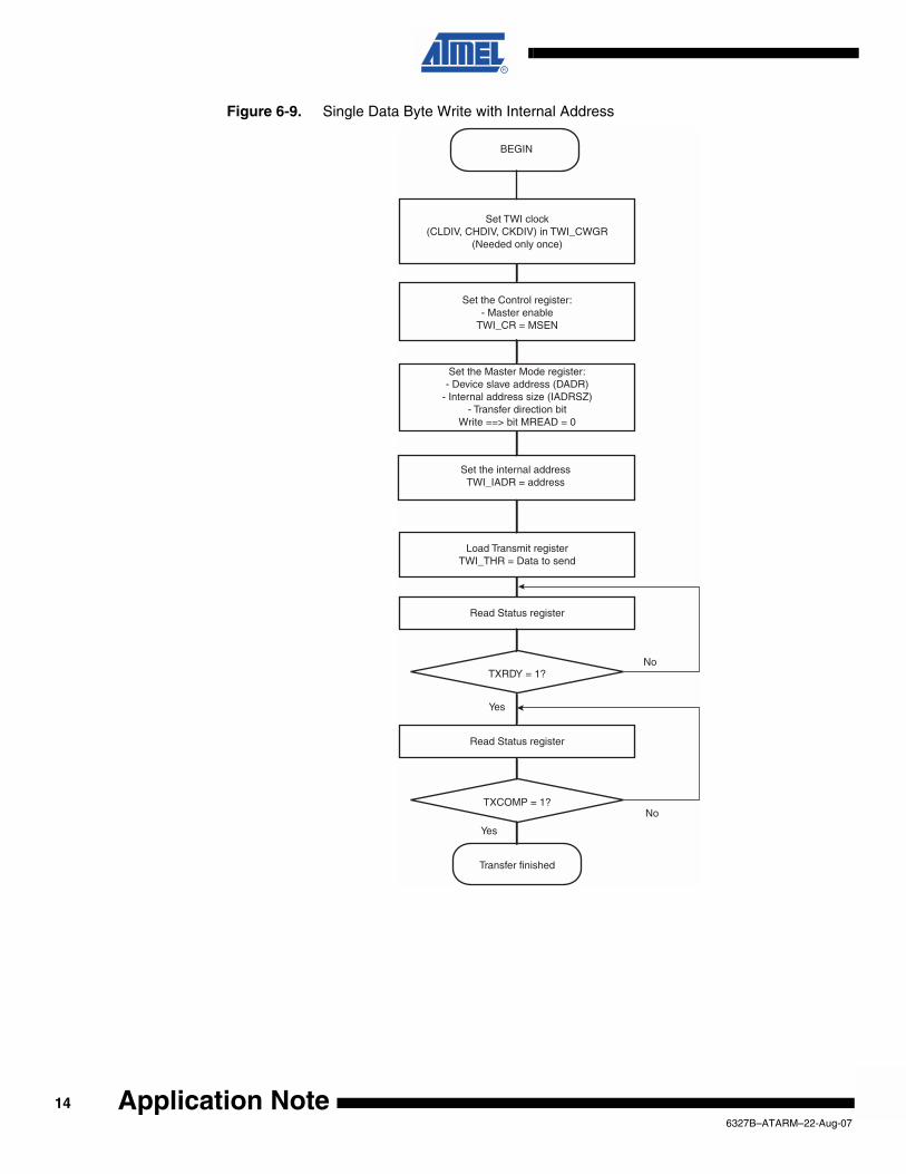
Figure 6-9. Single Data Byte Write with Internal Address
BEGIN
Set TWI clock(CLDIV, CHDIV, CKDIV) in TWI_CWGR
(Needed only once)
Set the Control register:- Master enable
TWI_CR = MSEN
Set the Master Mode register:- Device slave address (DADR)
- Internal address size (IADRSZ)- Transfer direction bit
Write ==> bit MREAD = 0
Load Transmit registerTWI_THR = Data to send
Read Status register
TXRDY = 1?
Read Status register
TXCOMP = 1?
Transfer finished
Set the internal addressTWI_IADR = address
Yes
Yes
No
No
146327B–ATARM–22-Aug-07
Application Note
Application Note
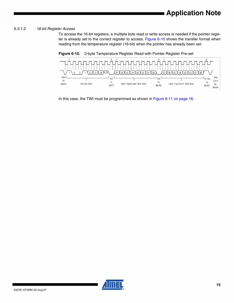
6.3.1.2 16-bit Register AccessTo access the 16-bit registers, a multiple byte read or write access is needed if the pointer regis-ter is already set to the correct register to access. Figure 6-10 shows the transfer format whenreading from the temperature register (16-bit) when the pointer has already been set.
Figure 6-10. 2-byte Temperature Register Read with Pointer Register Pre-set
In this case, the TWI must be programmed as shown in Figure 6-11 on page 16.
156327B–ATARM–22-Aug-07
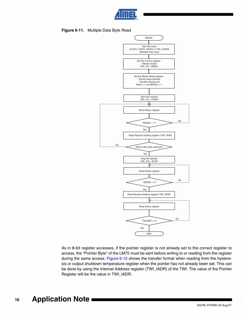
Figure 6-11. Multiple Data Byte Read
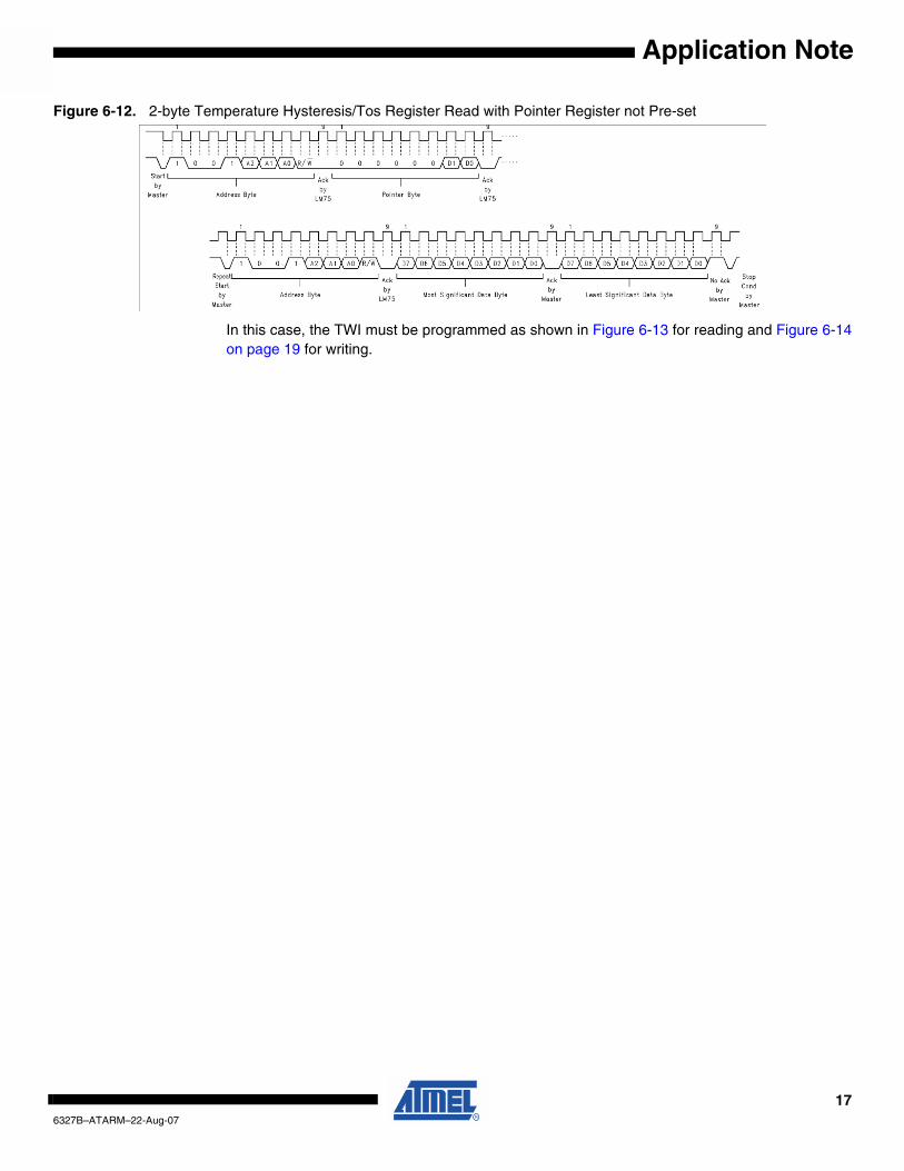
As in 8-bit register accesses, if the pointer register is not already set to the correct register toaccess, the “Pointer Byte” of the LM75 must be sent before writing to or reading from the registerduring the same access. Figure 6-12 shows the transfer format when reading from the hystere-sis or output shutdown temperature register when the pointer has not already been set. This canbe done by using the Internal Address register (TWI_IADR) of the TWI. The value of the PointerRegister will be the value in TWI_IADR.
Start the transferTWI_CR = START
Stop the transferTWI_CR = STOP
Read Status register
RXRDY = 1?
Next-to-last data received?
Read status register
TXCOMP = 1?
END
Yes
Yes
No
Yes
Read Receive Holding register (TWI_RHR)
No
Set the Control register:- Master enable
TWI_CR = MSEN
Set the Master Mode register:- Device slave address- Transfer direction bit
Read ==> bit MREAD = 1
BEGIN
Set TWI clock(CLDIV, CHDIV, CKDIV) in TWI_CWGR
(Needed only once)
No
Read Status register
RXRDY = 1?
Yes
Read Receive Holding register (TWI_RHR)
No
166327B–ATARM–22-Aug-07
Application Note
Application Note
Figure 6-12. 2-byte Temperature Hysteresis/Tos Register Read with Pointer Register not Pre-set
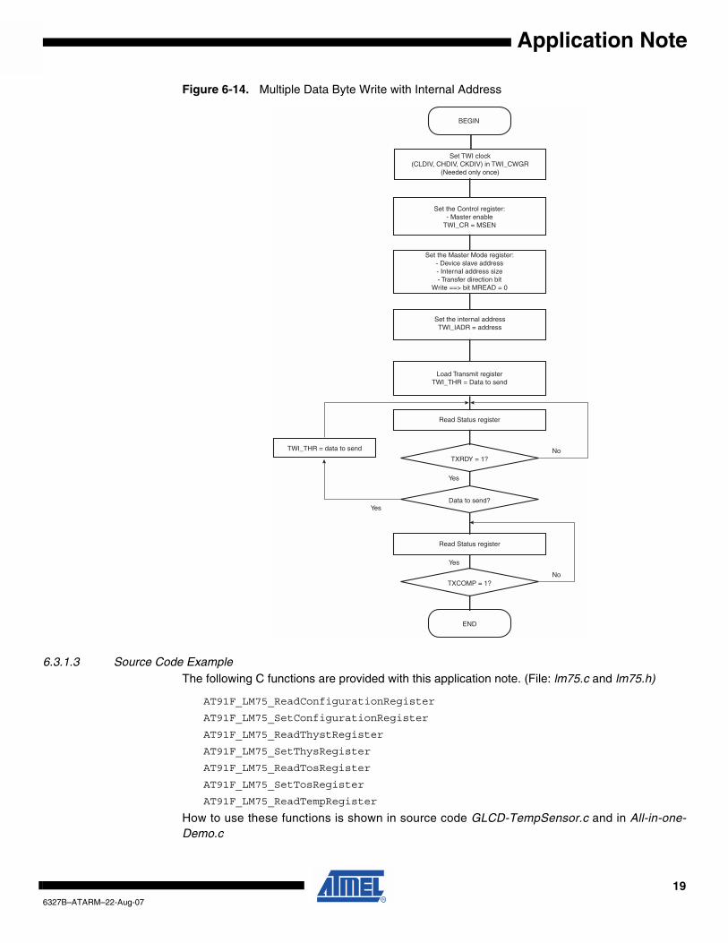
In this case, the TWI must be programmed as shown in Figure 6-13 for reading and Figure 6-14on page 19 for writing.
176327B–ATARM–22-Aug-07
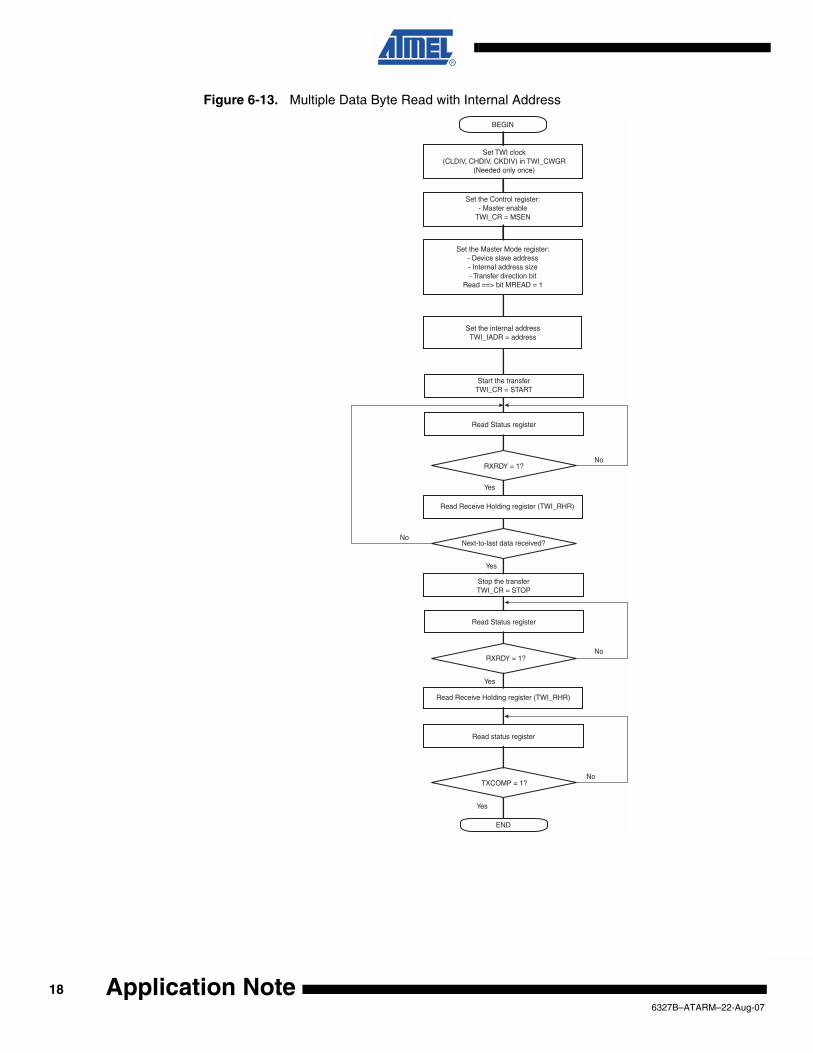
Figure 6-13. Multiple Data Byte Read with Internal Address
Start the transferTWI_CR = START
Stop the transferTWI_CR = STOP
Read Status register
RXRDY = 1?
Next-to-last data received?
Read status register
TXCOMP = 1?
END
Set the internal addressTWI_IADR = address
Yes
Yes
No
Yes
Read Receive Holding register (TWI_RHR)
No
Set the Control register:- Master enable
TWI_CR = MSEN
Set the Master Mode register:- Device slave address- Internal address size- Transfer direction bit
Read ==> bit MREAD = 1
BEGIN
Set TWI clock(CLDIV, CHDIV, CKDIV) in TWI_CWGR
(Needed only once)
No
Read Status register
RXRDY = 1?
Yes
Read Receive Holding register (TWI_RHR)
No
186327B–ATARM–22-Aug-07
Application Note
Application Note
Figure 6-14. Multiple Data Byte Write with Internal Address
6.3.1.3 Source Code ExampleThe following C functions are provided with this application note. (File: lm75.c and lm75.h)
AT91F_LM75_ReadConfigurationRegister
AT91F_LM75_SetConfigurationRegister
AT91F_LM75_ReadThystRegister
AT91F_LM75_SetThysRegister
AT91F_LM75_ReadTosRegister
AT91F_LM75_SetTosRegister
AT91F_LM75_ReadTempRegister
How to use these functions is shown in source code GLCD-TempSensor.c and in All-in-one-Demo.c
Set the Control register:- Master enable
TWI_CR = MSEN
Set the Master Mode register:- Device slave address- Internal address size- Transfer direction bit
Write ==> bit MREAD = 0
Load Transmit registerTWI_THR = Data to send
Read Status register
TXRDY = 1?
Data to send?
Read Status register
TXCOMP = 1?
END
BEGIN
Set the internal addressTWI_IADR = address
TWI_THR = data to send
Yes
Yes
Yes
No
No
Set TWI clock(CLDIV, CHDIV, CKDIV) in TWI_CWGR
(Needed only once)
196327B–ATARM–22-Aug-07
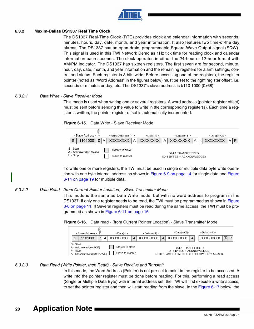
6.3.2 Maxim-Dallas DS1337 Real Time ClockThe DS1337 Real-Time Clock (RTC) provides clock and calendar information with seconds,minutes, hours, day, date, month, and year information. It also features two time-of-the dayalarms. The DS1337 has an open-drain, programmable Square-Wave Output signal (SQW).This signal is used in this TWI Network Demo as 1Hz tick time for reading clock and calendarinformation each seconds. The clock operates in either the 24-hour or 12-hour format withAM/PM indicator. The DS1337 has sixteen registers. The first seven are for second, minute,hour, day, date, month, and year information and the remaining registers for alarm settings, con-trol and status. Each register is 8 bits wide. Before accessing one of the registers, the registerpointer (noted as “Word Address” in the figures below) must be set to the right register offset, i.e.seconds or minutes or day, etc. The DS1337’s slave address is b110 1000 (0x68).
6.3.2.1 Data Write - Slave Receiver ModeThis mode is used when writing one or several registers. A word address (pointer register offset)must be sent before sending the value to write in the corresponding register(s). Each time a reg-ister is written, the pointer register offset is automatically incremented.
Figure 6-15. Data Write - Slave Receiver Mode
To write one or more registers, the TWI must be used in single or multiple data byte write opera-tion with one byte internal address as shown in Figure 6-9 on page 14 for single data and Figure6-14 on page 19 for multiple data.
6.3.2.2 Data Read - (from Current Pointer Location) - Slave Transmitter ModeThis mode is the same as Data Write mode, but with no word address to program in theDS1337. If only one register needs to be read, the TWI must be programmed as shown in Figure6-6 on page 11. If Several registers must be read during the same access, the TWI must be pro-grammed as shown in Figure 6-11 on page 16.
Figure 6-16. Data read - (from Current Pointer Location) - Slave Transmitter Mode
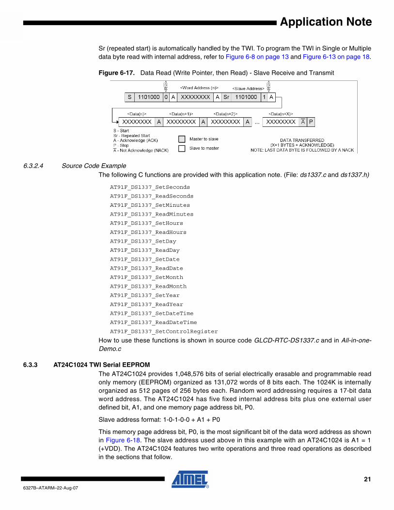
6.3.2.3 Data Read (Write Pointer, then Read) - Slave Receive and TransmitIn this mode, the Word Address (Pointer) is not pre-set to point to the register to be accessed. Awrite into the pointer register must be done before reading. For this, performing a read access(Single or Multiple Data Byte) with internal address set, the TWI will first execute a write access,to set the pointer register and then will start reading from the slave. In the Figure 6-17 below, the
206327B–ATARM–22-Aug-07
Application Note
Application Note
Sr (repeated start) is automatically handled by the TWI. To program the TWI in Single or Multipledata byte read with internal address, refer to Figure 6-8 on page 13 and Figure 6-13 on page 18.
Figure 6-17. Data Read (Write Pointer, then Read) - Slave Receive and Transmit
6.3.2.4 Source Code ExampleThe following C functions are provided with this application note. (File: ds1337.c and ds1337.h)
AT91F_DS1337_SetSeconds
AT91F_DS1337_ReadSeconds
AT91F_DS1337_SetMinutes
AT91F_DS1337_ReadMinutes
AT91F_DS1337_SetHours
AT91F_DS1337_ReadHours
AT91F_DS1337_SetDay
AT91F_DS1337_ReadDay
AT91F_DS1337_SetDate
AT91F_DS1337_ReadDate
AT91F_DS1337_SetMonth
AT91F_DS1337_ReadMonth
AT91F_DS1337_SetYear
AT91F_DS1337_ReadYear
AT91F_DS1337_SetDateTime
AT91F_DS1337_ReadDateTime
AT91F_DS1337_SetControlRegister
How to use these functions is shown in source code GLCD-RTC-DS1337.c and in All-in-one-Demo.c
6.3.3 AT24C1024 TWI Serial EEPROMThe AT24C1024 provides 1,048,576 bits of serial electrically erasable and programmable readonly memory (EEPROM) organized as 131,072 words of 8 bits each. The 1024K is internallyorganized as 512 pages of 256 bytes each. Random word addressing requires a 17-bit dataword address. The AT24C1024 has five fixed internal address bits plus one external userdefined bit, A1, and one memory page address bit, P0.
Slave address format: 1-0-1-0-0 + A1 + P0
This memory page address bit, P0, is the most significant bit of the data word address as shownin Figure 6-18. The slave address used above in this example with an AT24C1024 is A1 = 1(+VDD). The AT24C1024 features two write operations and three read operations as describedin the sections that follow.
216327B–ATARM–22-Aug-07
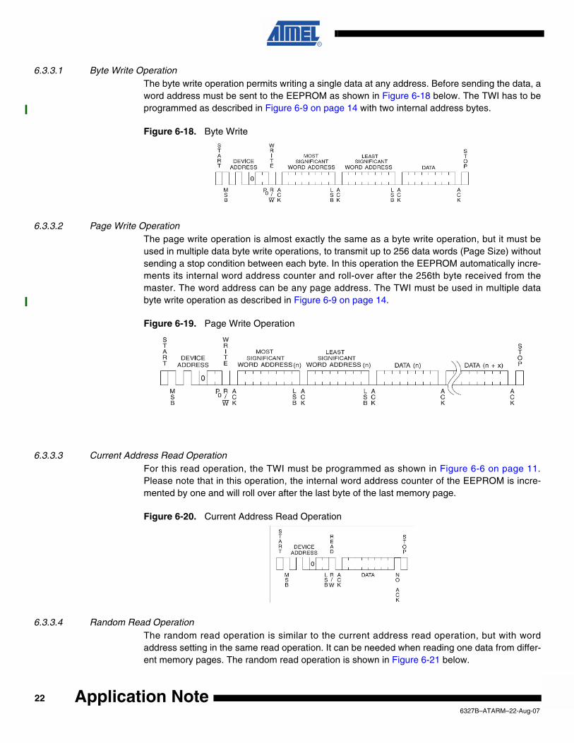
6.3.3.1 Byte Write OperationThe byte write operation permits writing a single data at any address. Before sending the data, aword address must be sent to the EEPROM as shown in Figure 6-18 below. The TWI has to beprogrammed as described in Figure 6-9 on page 14 with two internal address bytes.
Figure 6-18. Byte Write
6.3.3.2 Page Write OperationThe page write operation is almost exactly the same as a byte write operation, but it must beused in multiple data byte write operations, to transmit up to 256 data words (Page Size) withoutsending a stop condition between each byte. In this operation the EEPROM automatically incre-ments its internal word address counter and roll-over after the 256th byte received from themaster. The word address can be any page address. The TWI must be used in multiple databyte write operation as described in Figure 6-9 on page 14.
Figure 6-19. Page Write Operation
6.3.3.3 Current Address Read OperationFor this read operation, the TWI must be programmed as shown in Figure 6-6 on page 11.Please note that in this operation, the internal word address counter of the EEPROM is incre-mented by one and will roll over after the last byte of the last memory page.
Figure 6-20. Current Address Read Operation
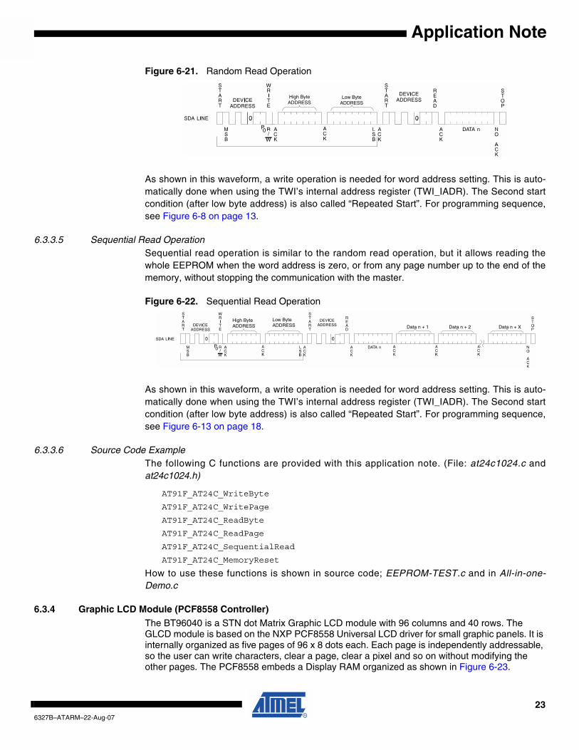
6.3.3.4 Random Read OperationThe random read operation is similar to the current address read operation, but with wordaddress setting in the same read operation. It can be needed when reading one data from differ-ent memory pages. The random read operation is shown in Figure 6-21 below.
226327B–ATARM–22-Aug-07
Application Note
Application Note
Figure 6-21. Random Read Operation
As shown in this waveform, a write operation is needed for word address setting. This is auto-matically done when using the TWI’s internal address register (TWI_IADR). The Second startcondition (after low byte address) is also called “Repeated Start”. For programming sequence,see Figure 6-8 on page 13.
6.3.3.5 Sequential Read OperationSequential read operation is similar to the random read operation, but it allows reading thewhole EEPROM when the word address is zero, or from any page number up to the end of thememory, without stopping the communication with the master.
Figure 6-22. Sequential Read Operation
As shown in this waveform, a write operation is needed for word address setting. This is auto-matically done when using the TWI’s internal address register (TWI_IADR). The Second startcondition (after low byte address) is also called “Repeated Start”. For programming sequence,see Figure 6-13 on page 18.
6.3.3.6 Source Code ExampleThe following C functions are provided with this application note. (File: at24c1024.c andat24c1024.h)
AT91F_AT24C_WriteByte
AT91F_AT24C_WritePage
AT91F_AT24C_ReadByte
AT91F_AT24C_ReadPage
AT91F_AT24C_SequentialRead
AT91F_AT24C_MemoryReset
How to use these functions is shown in source code; EEPROM-TEST.c and in All-in-one-Demo.c
6.3.4 Graphic LCD Module (PCF8558 Controller)The BT96040 is a STN dot Matrix Graphic LCD module with 96 columns and 40 rows. The GLCD module is based on the NXP PCF8558 Universal LCD driver for small graphic panels. It is internally organized as five pages of 96 x 8 dots each. Each page is independently addressable, so the user can write characters, clear a page, clear a pixel and so on without modifying the other pages. The PCF8558 embeds a Display RAM organized as shown in Figure 6-23.
P0
High ByteADDRESS
Low ByteADDRESS
P0
High ByteADDRESS
Low ByteADDRESS Data n + 1 Data n + 2 Data n + X
236327B–ATARM–22-Aug-07
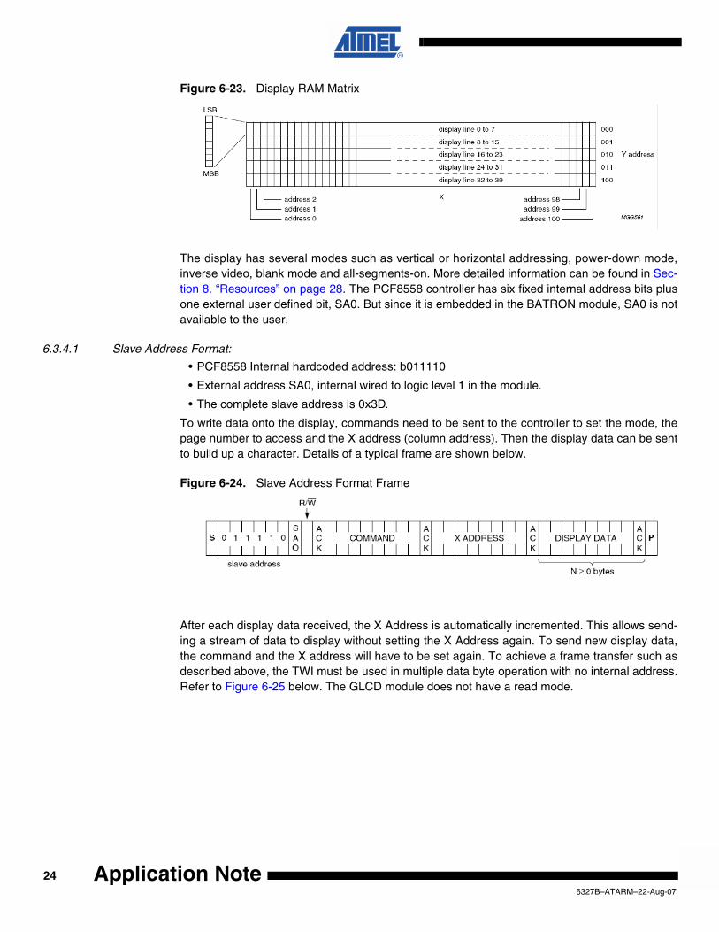
Figure 6-23. Display RAM Matrix
The display has several modes such as vertical or horizontal addressing, power-down mode,inverse video, blank mode and all-segments-on. More detailed information can be found in Sec-tion 8. “Resources” on page 28. The PCF8558 controller has six fixed internal address bits plusone external user defined bit, SA0. But since it is embedded in the BATRON module, SA0 is notavailable to the user.
6.3.4.1 Slave Address Format:
• PCF8558 Internal hardcoded address: b011110
• External address SA0, internal wired to logic level 1 in the module.
• The complete slave address is 0x3D.
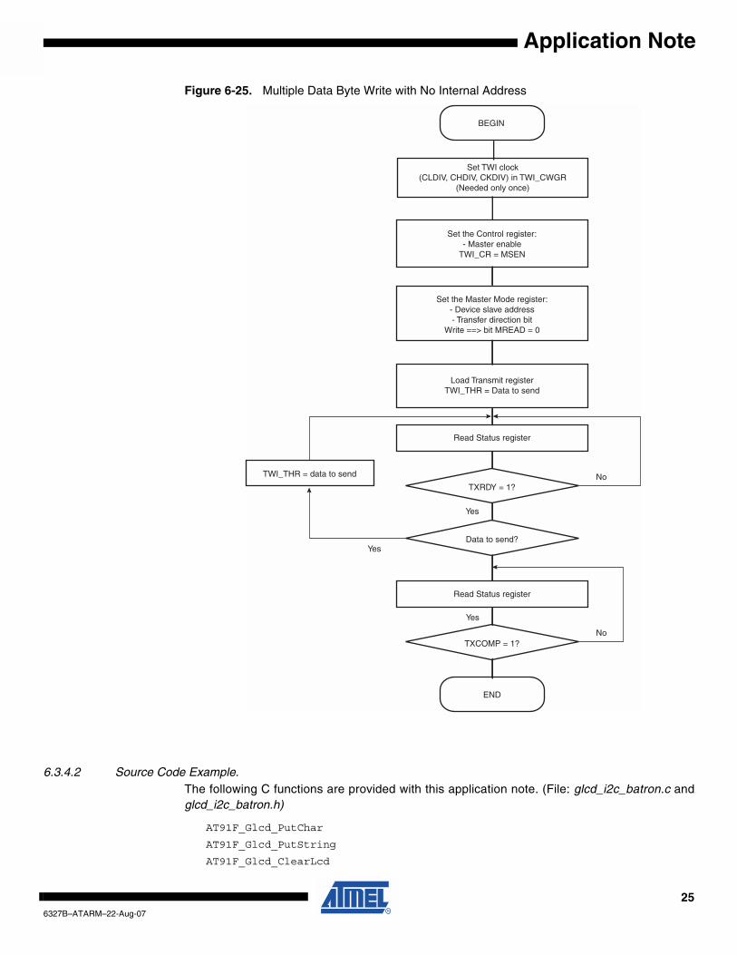
To write data onto the display, commands need to be sent to the controller to set the mode, thepage number to access and the X address (column address). Then the display data can be sentto build up a character. Details of a typical frame are shown below.
Figure 6-24. Slave Address Format Frame
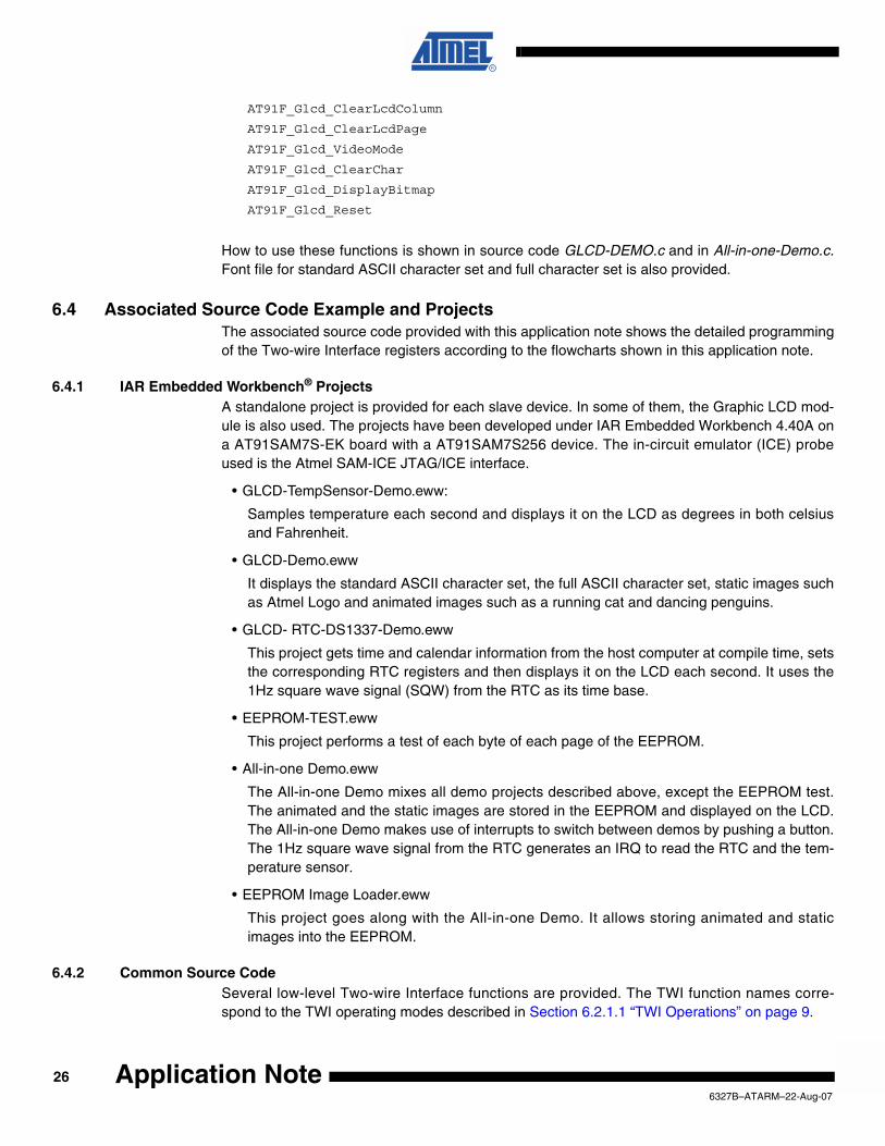
After each display data received, the X Address is automatically incremented. This allows send-ing a stream of data to display without setting the X Address again. To send new display data,the command and the X address will have to be set again. To achieve a frame transfer such asdescribed above, the TWI must be used in multiple data byte operation with no internal address.Refer to Figure 6-25 below. The GLCD module does not have a read mode.
246327B–ATARM–22-Aug-07
Application Note
Application Note
Figure 6-25. Multiple Data Byte Write with No Internal Address
6.3.4.2 Source Code Example.The following C functions are provided with this application note. (File: glcd_i2c_batron.c andglcd_i2c_batron.h)
AT91F_Glcd_PutChar
AT91F_Glcd_PutString
AT91F_Glcd_ClearLcd
Set the Control register:- Master enable
TWI_CR = MSEN
Set the Master Mode register:- Device slave address- Transfer direction bit
Write ==> bit MREAD = 0
Load Transmit registerTWI_THR = Data to send
Read Status register
TXRDY = 1?
Data to send?
Read Status register
TXCOMP = 1?
END
BEGIN
TWI_THR = data to send
Yes
Yes
Yes
No
No
Set TWI clock(CLDIV, CHDIV, CKDIV) in TWI_CWGR
(Needed only once)
256327B–ATARM–22-Aug-07
AT91F_Glcd_ClearLcdColumn
AT91F_Glcd_ClearLcdPage
AT91F_Glcd_VideoMode
AT91F_Glcd_ClearChar
AT91F_Glcd_DisplayBitmap
AT91F_Glcd_Reset
How to use these functions is shown in source code GLCD-DEMO.c and in All-in-one-Demo.c.Font file for standard ASCII character set and full character set is also provided.
6.4 Associated Source Code Example and ProjectsThe associated source code provided with this application note shows the detailed programmingof the Two-wire Interface registers according to the flowcharts shown in this application note.
6.4.1 IAR Embedded Workbench® ProjectsA standalone project is provided for each slave device. In some of them, the Graphic LCD mod-ule is also used. The projects have been developed under IAR Embedded Workbench 4.40A ona AT91SAM7S-EK board with a AT91SAM7S256 device. The in-circuit emulator (ICE) probeused is the Atmel SAM-ICE JTAG/ICE interface.
• GLCD-TempSensor-Demo.eww:
Samples temperature each second and displays it on the LCD as degrees in both celsiusand Fahrenheit.
• GLCD-Demo.eww
It displays the standard ASCII character set, the full ASCII character set, static images suchas Atmel Logo and animated images such as a running cat and dancing penguins.
• GLCD- RTC-DS1337-Demo.eww
This project gets time and calendar information from the host computer at compile time, setsthe corresponding RTC registers and then displays it on the LCD each second. It uses the1Hz square wave signal (SQW) from the RTC as its time base.
• EEPROM-TEST.eww
This project performs a test of each byte of each page of the EEPROM.
• All-in-one Demo.eww
The All-in-one Demo mixes all demo projects described above, except the EEPROM test.The animated and the static images are stored in the EEPROM and displayed on the LCD.The All-in-one Demo makes use of interrupts to switch between demos by pushing a button.The 1Hz square wave signal from the RTC generates an IRQ to read the RTC and the tem-perature sensor.
• EEPROM Image Loader.eww
This project goes along with the All-in-one Demo. It allows storing animated and staticimages into the EEPROM.
6.4.2 Common Source CodeSeveral low-level Two-wire Interface functions are provided. The TWI function names corre-spond to the TWI operating modes described in Section 6.2.1.1 “TWI Operations” on page 9.
266327B–ATARM–22-Aug-07
Application Note
Application Note
AT91F_TWI_Open
AT91F_TWI_WriteSingle
AT91F_TWI_WriteSingleIadr
AT91F_TWI_WriteMultiple
AT91F_TWI_WriteMultipleIadr
AT91F_TWI_ReadSingle
AT91F_TWI_ReadSingleIadr
AT91F_TWI_ReadMultiple
AT91F_TWI_ReadMultipleIadr
AT91F_TWI_BusRecovery
AT91F_TWI_WaitMicroSecond
AT91F_TWI_ProbeDevices
6.4.3 Porting GuideThe code provided here, is for one of the first AT91SAM member in which the Two-wire interfaceonly supports the master mode. For some newer AT91SAM devices, it may happen that a newTwo-wire Interface peripheral is embedded with support for slave and multi-master TWI/I²Cmode. Check the device’s datasheet that you are using. This does not prevent to use most of thecode provided. The main difference between TWI peripheral with master mode only and TWIperipheral with Master, Multi-Master and Slave mode, is the formula to set the TWI bit rate.
The IAR embedded workbench projects as described in Section 6.4.1 on page 26 are providedfor the AT91SAM7SE-EK board in AN-AT91SAM-TWI-software file associated with this applica-tion note.
7. TroubleshootingThe following FAQs give some suggestions in case of TWI malfunction.
• “After a system reset, I am not able to initiate a new TWI transfer, only power supply cycling of the whole system solves the problem.”
→ As described in Section 5.5.2 “Resetting a TWI/I²C Slave Device” on page 7, the slavedevice and TWI/I²C bus may be hung up.
• “When I perform a multiple data read, the TWI reads one more byte from the slave.”
→ This can happen when the STOP condition has not been set during the next-to-last datareceived.
• “I set the TWI clock to be 100 KHz or 400 KHz, but I see less than that.”
→ Due to the clock stretching capability of the TWI, this may happen if the pull-up resistors(Rp) are not computed correctly (too weak) versus the bus capacitance (Cbus), or the esti-mated bus capacitance is not good. If the pull-ups are weak, the rise time will be higher thanspecified and the TWI may interpret it as though a slave device is stretching the clock, thusresulting in a lower frequency.
• In Master transmitter Mode, I sometimes do not have the right number of data transmitted (less data) and the TWI ends the transfer by sending a STOP condition.
→ This may happen when several IRQs are used in the system. It may happen, that the TWItransfer is interrupted by another task of the system. If the Transmit Holding Register
276327B–ATARM–22-Aug-07
(TWI_THR) is not written fast enough, the TWI ends the transfer by sending a stopcondition.
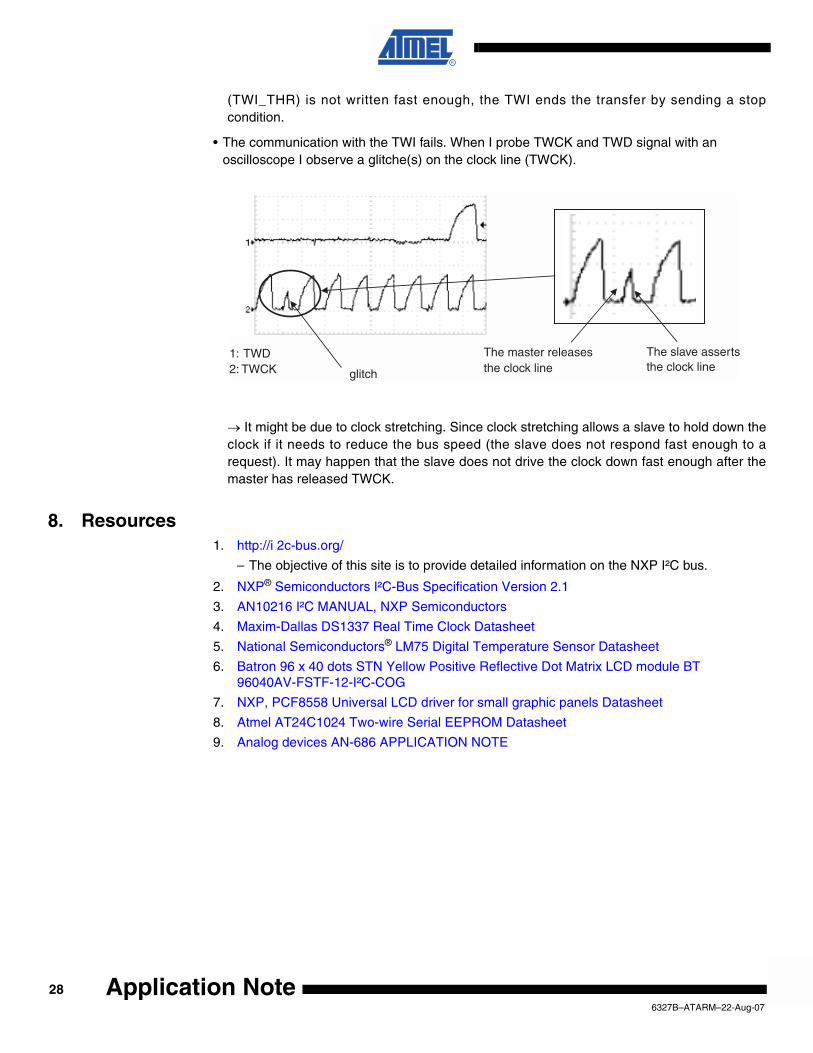
• The communication with the TWI fails. When I probe TWCK and TWD signal with an oscilloscope I observe a glitche(s) on the clock line (TWCK).
→ It might be due to clock stretching. Since clock stretching allows a slave to hold down theclock if it needs to reduce the bus speed (the slave does not respond fast enough to arequest). It may happen that the slave does not drive the clock down fast enough after themaster has released TWCK.
8. Resources1. http://i 2c-bus.org/
– The objective of this site is to provide detailed information on the NXP I²C bus.
2. NXP® Semiconductors I²C-Bus Specification Version 2.1
3. AN10216 I²C MANUAL, NXP Semiconductors
4. Maxim-Dallas DS1337 Real Time Clock Datasheet
5. National Semiconductors® LM75 Digital Temperature Sensor Datasheet
6. Batron 96 x 40 dots STN Yellow Positive Reflective Dot Matrix LCD module BT 96040AV-FSTF-12-I²C-COG
7. NXP, PCF8558 Universal LCD driver for small graphic panels Datasheet
8. Atmel AT24C1024 Two-wire Serial EEPROM Datasheet
9. Analog devices AN-686 APPLICATION NOTE
1: TWD2: TWCK glitch
The slave assertsthe clock line
The master releasesthe clock line
286327B–ATARM–22-Aug-07
Application Note
Application Note
Revision History
Doc. Rev Comments
Change Request Ref.
6327B
Figure 5-1“Application Block Diagram” on page 3, repositioned.
Section 6.1 “Transfer Format” on page 8, placement of Figure 6-1 and Figure 6-2 swapped and relocated.Section 6.2.1 “Internal Address” on page 9,renamed Figure 6-3 and Figure 6-4 and updated Figure 6-3.
Section 6.3.2.1 “Data Write - Slave Receiver Mode”, updated cross references and removed two flowcharts from end of section with subsequent change to figure-number assignments (after 6-15).
Section 6.3.3.1 “Byte Write Operation” and Section 6.3.3.2 “Page Write Operation” cross references to flowcharts updated.
4693
6327A First issue
296327B–ATARM–22-Aug-07
6327B–ATARM–22-Aug-07
Headquarters International
Atmel Corporation2325 Orchard ParkwaySan Jose, CA 95131USATel: 1(408) 441-0311Fax: 1(408) 487-2600
Atmel AsiaRoom 1219Chinachem Golden Plaza77 Mody Road TsimshatsuiEast KowloonHong KongTel: (852) 2721-9778Fax: (852) 2722-1369
Atmel EuropeLe Krebs8, Rue Jean-Pierre TimbaudBP 30978054 Saint-Quentin-en-Yvelines CedexFranceTel: (33) 1-30-60-70-00 Fax: (33) 1-30-60-71-11
Atmel Japan9F, Tonetsu Shinkawa Bldg.1-24-8 ShinkawaChuo-ku, Tokyo 104-0033JapanTel: (81) 3-3523-3551Fax: (81) 3-3523-7581
Product Contact
Web Sitewww.atmel.com
Technical SupportEnter Product Line E-mail
Sales Contactwww.atmel.com/contacts
Web Sitewww.atmel.comwww.atmel.com/AT91SAM
Technical SupportAT91SAM SupportAtmel techincal support
Sales Contactswww.atmel.com/contacts/
Literature Requestswww.atmel.com/literature
Disclaimer: The information in this document is provided in connection with Atmel products. No license, express or implied, by estoppel or otherwise, to anyintellectual property right is granted by this document or in connection with the sale of Atmel products. EXCEPT AS SET FORTH IN ATMEL’S TERMS AND CONDI-TIONS OF SALE LOCATED ON ATMEL’S WEB SITE, ATMEL ASSUMES NO LIABILITY WHATSOEVER AND DISCLAIMS ANY EXPRESS, IMPLIED OR STATUTORYWARRANTY RELATING TO ITS PRODUCTS INCLUDING, BUT NOT LIMITED TO, THE IMPLIED WARRANTY OF MERCHANTABILITY, FITNESS FOR A PARTICULARPURPOSE, OR NON-INFRINGEMENT. IN NO EVENT SHALL ATMEL BE LIABLE FOR ANY DIRECT, INDIRECT, CONSEQUENTIAL, PUNITIVE, SPECIAL OR INCIDEN-TAL DAMAGES (INCLUDING, WITHOUT LIMITATION, DAMAGES FOR LOSS OF PROFITS, BUSINESS INTERRUPTION, OR LOSS OF INFORMATION) ARISING OUTOF THE USE OR INABILITY TO USE THIS DOCUMENT, EVEN IF ATMEL HAS BEEN ADVISED OF THE POSSIBILITY OF SUCH DAMAGES. Atmel makes norepresentations or warranties with respect to the accuracy or completeness of the contents of this document and reserves the right to make changes to specifica-tions and product descriptions at any time without notice. Atmel does not make any commitment to update the information contained herein. Unless specifically pro-vided otherwise, Atmel products are not suitable for, and shall not be used in, automotive applications. Atmel’s products are not intended, authorized, or warrantedfor use as components in applications intended to support or sustain life.
© 2007 Atmel Corporation. All rights reserved. Atmel®, logo and combinations thereof and others, are registered trademarks or trademarks ofAtmel Corporation or its subsidiaries. ARM®, the ARMPowered® logo, Thumb® are registered trademarks of ARM Ltd. Other terms and productnames may be trademarks of others.


![An01 Cons Fr[1]](https://img.pdfslide.net/doc/110x75/55cf9aa2550346d033a2aefd/an01-cons-fr1.jpg)