Embed Size (px)
Citation preview

CKA(PF)
I KA(P
A)
0.0001 0.001 0.01 0.1 1 1020
100
1000
2000
STABLE
D001
Vref
Input VKA
IKA
Product
Folder
Order
Now
Technical
Documents
Tools &
Software
Support &Community
ReferenceDesign
An IMPORTANT NOTICE at the end of this data sheet addresses availability, warranty, changes, use in safety-critical applications,intellectual property matters and other important disclaimers. PRODUCTION DATA.
ATL431, ATL432SLVSCV5D –MARCH 2015–REVISED OCTOBER 2016
ATL431, ATL432 2.5-V Low Iq Adjustable Precision Shunt Regulator
1
1 Features1• Adjustable Regulated Output of 2.5 V to 36 V• Very-Low Operating Current
– IKA(min) = 35 µA (Max)– IREF = 150 nA (Max)
• Internally Compensated for Stability– Stable With No Capacitive Load
• Reference Voltage Tolerances at 25°C– 0.5% for B Grade– 1% for A Grade
• Typical Temperature Drift– 5 mV (–40°C to +85°C); I Version– 6 mV (–40°C to +125°C); Q Version
• Extended Cathode Current Range35 µA to 100 mA
• Low Output Impedance of 0.3 Ω (Max)
2 Applications• Secondary Side Regulation in Flyback SMPSs• Industrial, Computing, Consumer, and Portables• Adjustable Voltage and Current Referencing• Power Management• Power Isolation• Zener Replacement
3 DescriptionThe ATL431 and ATL432 are three-terminaladjustable shunt regulators, with specified thermalstability over applicable automotive, commercial, andindustrial temperature ranges. The output voltage canbe set to any value between Vref (approximately2.5 V) and 36 V, with two external resistors. Thesedevices have a typical output impedance of 0.05 Ω.Active output circuitry provides a very sharp turn-oncharacteristic, making these devices excellentreplacements for Zener diodes in many applications,such as onboard regulation, adjustable powersupplies, and switching power supplies.
The ATL43x has > 20x improvement cathode currentrange over it's TL43x predecessor. It also is stablewith a wider range of load capacitance types andvalues.
ATL431 and ATL432 are the exact same parts butwith different pinouts and order numbers. TheATL43x is offered in two grades, with initialtolerances (at 25°C) of 0.5%, 1%, for the B and Agrade, respectively. In addition, low output drift vstemperature ensures consistent voltage regulationover the entire temperature range.
The ATL43xxI devices are characterized for operationfrom –40°C to +85°C, and the ATL43xxQ devices arecharacterized for operation from –40°C to +125°C.
Device Information(1)
PART NUMBER PACKAGE BODY SIZE (NOM)ATL431ATL432 SOT (3) 2.90 mm × 1.60 mm
(1) For all available packages, see the orderable addendum atthe end of the data sheet.
Simplified Schematic Stability Region for VKA = 15.0 V

2
ATL431, ATL432SLVSCV5D –MARCH 2015–REVISED OCTOBER 2016 www.ti.com
Product Folder Links: ATL431 ATL432
Submit Documentation Feedback Copyright © 2015–2016, Texas Instruments Incorporated
Table of Contents1 Features .................................................................. 12 Applications ........................................................... 13 Description ............................................................. 14 Revision History..................................................... 25 Pin Configuration and Functions ......................... 36 Specifications......................................................... 3
6.1 Absolute Maximum Ratings ..................................... 36.2 ESD Ratings.............................................................. 36.3 Recommended Operating Conditions....................... 36.4 Thermal Information .................................................. 46.5 Electrical Characteristics, ATL431Ax, ATL432Ax ..... 46.6 Electrical Characteristics, ATL431Bx, ATL432Bx ..... 46.7 Typical Characteristics .............................................. 5
7 Parameter Measurement Information .................. 98 Detailed Description ............................................ 11
8.1 Overview ................................................................. 118.2 Functional Block Diagram ....................................... 11
8.3 Feature Description................................................. 118.4 Device Functional Modes........................................ 12
9 Application and Implementation ........................ 139.1 Application Information............................................ 139.2 Typical Applications ................................................ 14
10 Power Supply Recommendations ..................... 1811 Layout................................................................... 18
11.1 Layout Guidelines ................................................. 1811.2 Layout Example .................................................... 18
12 Device and Documentation Support ................. 1912.1 Related Links ........................................................ 1912.2 Receiving Notification of Documentation Updates 1912.3 Community Resources.......................................... 1912.4 Trademarks ........................................................... 1912.5 Electrostatic Discharge Caution............................ 1912.6 Glossary ................................................................ 19
13 Mechanical, Packaging, and OrderableInformation ........................................................... 19
4 Revision HistoryNOTE: Page numbers for previous revisions may differ from page numbers in the current version.
Changes from Revision C (September 2015) to Revision D Page
• Changed Small-Signal Voltage Amplification vs Frequency with an updated graph to provide additional data .................... 6• Changed Test Circuit for Phase and Gain Measurement with an updated schematic........................................................... 9• Updated Comparator Mode specifications in Design Parameters........................................................................................ 14• Added Receiving Notification of Documentation Updates section ....................................................................................... 19
Changes from Revision B (May 2015) to Revision C Page
• Changed ATL432xx status from PREVIEW to PRODUCTION. ............................................................................................. 1
Changes from Revision A (April 2015) to Revision B Page
• Changed ATL431AQ, ATL431BI and ATL431BQ status from PREVIEW to PRODUCTION. ............................................... 1• Changed flyback schematic to represent a more robust design ......................................................................................... 13• Added flyback supply reliability recommendation................................................................................................................. 18
Changes from Original (March 2013) to Revision A Page
• Initial release of full verison. ................................................................................................................................................... 1

1REF
2CATHODE
3 ANODE
Not to scale
1CATHODE
2REF
3 ANODE
Not to scale
3
ATL431, ATL432www.ti.com SLVSCV5D –MARCH 2015–REVISED OCTOBER 2016
Product Folder Links: ATL431 ATL432
Submit Documentation FeedbackCopyright © 2015–2016, Texas Instruments Incorporated
5 Pin Configuration and Functions
ATL431 DBZ Package3-Pin SOT-23
Top ViewATL432 DBZ Package
3-Pin SOT-23Top View
Pin FunctionsPIN
I/O DESCRIPTIONNAME
NO.ATL431x ATL432x
CATHODE 1 2 I/O Shunt Current/Voltage inputREF 2 1 I Threshold relative to common anodeANODE 3 3 O Common pin, normally connected to ground
(1) Stresses beyond those listed under Absolute Maximum Ratings may cause permanent damage to the device. These are stress ratingsonly, and functional operation of the device at these or any other conditions beyond those indicated under Recommended OperatingConditions is not implied. Exposure to absolute-maximum-rated conditions for extended periods may affect device reliability.
(2) All voltage values are with respect to ANODE, unless otherwise noted.
6 Specifications
6.1 Absolute Maximum Ratings (1)
over operating free-air temperature range (unless otherwise noted)MIN MAX UNIT
VKA Cathode voltage (2) 40 VIKA Continuous cathode current –100 150 mAII(ref) Reference input current –0.05 10 mATJ Operating virtual junction temperature –40 150 °CTstg Storage temperature –65 150 °C
(1) JEDEC document JEP155 states that 500-V HBM allows safe manufacturing with a standard ESD control process.(2) JEDEC document JEP157 states that 250-V CDM allows safe manufacturing with a standard ESD control process.
6.2 ESD RatingsVALUE UNIT
V(ESD) Electrostatic dischargeHuman-body model (HBM), per ANSI/ESDA/JEDEC JS-001 (1) ±2000
VCharged-device model (CDM), per JEDEC specification JESD22-C101 (2) ±1000
6.3 Recommended Operating ConditionsMIN MAX UNIT
VKA Cathode voltage Vref 36 VIKA Cathode current .035 100 mA
TA Operating free-air temperature"I" Grade –40 85
°C"Q" Grade –40 125

4
ATL431, ATL432SLVSCV5D –MARCH 2015–REVISED OCTOBER 2016 www.ti.com
Product Folder Links: ATL431 ATL432
Submit Documentation Feedback Copyright © 2015–2016, Texas Instruments Incorporated
(1) For more information about traditional and new thermal metrics, see the Semiconductor and IC Package Thermal Metrics applicationreport.
6.4 Thermal Information
THERMAL METRIC (1)ATL43xx
UNITDBZ (SOT-23)3 PINS
RθJA Junction-to-ambient thermal resistance 331.8 °C/WRθJC(top) Junction-to-case (top) thermal resistance 106.5 °C/WRθJB Junction-to-board thermal resistance 64.6 °C/WψJT Junction-to-top characterization parameter 4.9 °C/WψJB Junction-to-board characterization parameter 62.9 °C/W
6.5 Electrical Characteristics, ATL431Ax, ATL432Axover recommended operating conditions, TA = 25°C (unless otherwise noted)
PARAMETER TEST CIRCUIT TEST CONDITIONS MIN TYP MAX UNITVref Reference voltage Figure 22 VKA = Vref, IKA = 1 mA 2475 2500 2525 mV
VI(dev)
Deviation of reference inputvoltage over full temperaturerange, see section
Figure 22 VKA = Vref,IKA = 1 mA,
ATL43xAI; TA =-40°C to 85°C 5 15
mVATL43xAQ; TA =-40°C to 125°C 6 34
ΔVref / ΔVKA
Ratio of change in referencevoltage to the change incathode voltage
Figure 23 IKA = 1 mAΔVKA = 10 V − Vref –0.4 –2.7
mV/VΔVKA = 36 V − 10 V –0.1 –2
Iref Reference input current Figure 23 IKA = 1 mA, R1 = 10 kΩ, R2 = ∞ 30 150 nA
II(dev)
Deviation of reference inputcurrent over full temperaturerange, see section
Figure 23 IKA = 1 mA, R1 = 10 kΩ, R2 = ∞ 20 50 nA
IminMinimum cathode current forregulation
Figure 22Figure 5 VKA = Vref 20 35 µA
Ioff Off-state cathode current Figure 24 VKA = 36 V, Vref = 0 0.05 0.2 µA
|zKA| Dynamic impedance, seesection Figure 22 VKA = Vref, f ≤ 1 kHz,
IKA = 1 mA to 100 mA 0.05 0.3 Ω
6.6 Electrical Characteristics, ATL431Bx, ATL432Bxover recommended operating conditions, TA = 25°C (unless otherwise noted)
PARAMETER TEST CIRCUIT TEST CONDITIONS MIN TYP MAX UNITVref Reference voltage Figure 22 VKA = Vref, IKA = 1 mA 2487 2500 2512 mV
VI(dev)
Deviation of reference inputvoltage over full temperaturerange, see section
Figure 22 VKA = Vref, IKA = 1mA
ATL43xBI; TA =–40°C to 85°C 5 15
mVATL43xBQ; TA =–40°C to 125°C 6 34
ΔVref /ΔVKA
Ratio of change in referencevoltage to the change incathode voltage
Figure 23 IKA = 1 mAΔVKA = 10 V − Vref –0.4 –2.7
mV/VΔVKA = 36 V − 10 V –0.1 –2
Iref Reference input current Figure 23 IKA = 1 mA, R1 = 10 kΩ, R2 = ∞ 30 150 nA
II(dev)
Deviation of reference inputcurrent over full temperaturerange, see section
Figure 23 IKA = 1 mA, R1 = 10 kΩ, R2 = ∞ 20 50 nA
IminMinimum cathode current forregulation
Figure 22Figure 5 VKA = Vref 20 35 µA
Ioff Off-state cathode current Figure 24 VKA = 36 V, Vref = 0 0.05 0.2 µA
|zKA| Dynamic impedance, seesection Figure 22 VKA = Vref, f ≤ 1 kHz, IKA = 1 mA to 100 mA 0.05 0.3 Ω
VKA = VREF (V)
I KA (P
A)
2.3 2.35 2.4 2.45 2.5 2.5510
15
20
25
30
Ik(min)
TA (qC)
I OF
F (P
A)
-40 -20 0 20 40 60 80 100 120 1400
0.04
0.08
0.12
0.16
0.2
VKA = VREF (V)
I KA (
mA
)
-1.5 -1 -0.5 0 0.5 1 1.5 2 2.5 3-100
-80
-60
-40
-20
0
20
40
60
80
100
D001 VKA = VREF (V)
I KA (P
A)
0 0.5 1 1.5 2 2.5 30
10
20
30
40
D001
TA = -40qCTA = 25qCTA = 85qCTA = 125qC
TA (qC)
Vre
f (m
V)
-40 -20 0 20 40 60 80 100 120 1402475
2480
2485
2490
2495
2500
2505
2510
2515
2520Vref = 2485mVVref = 2500mVVref = 2504mV
TA (qC)
I RE
F (P
A)
-40 -20 0 20 40 60 80 100 120 1400
0.008
0.016
0.024
0.032
0.04
5
ATL431, ATL432www.ti.com SLVSCV5D –MARCH 2015–REVISED OCTOBER 2016
Product Folder Links: ATL431 ATL432
Submit Documentation FeedbackCopyright © 2015–2016, Texas Instruments Incorporated
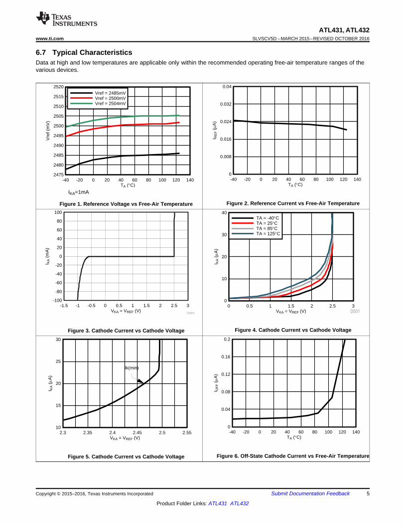
6.7 Typical CharacteristicsData at high and low temperatures are applicable only within the recommended operating free-air temperature ranges of thevarious devices.
IKA=1mA
Figure 1. Reference Voltage vs Free-Air Temperature Figure 2. Reference Current vs Free-Air Temperature
Figure 3. Cathode Current vs Cathode Voltage Figure 4. Cathode Current vs Cathode Voltage
Figure 5. Cathode Current vs Cathode Voltage Figure 6. Off-State Cathode Current vs Free-Air Temperature

Frequency (Hz)
Out
put I
mpe
danc
e (:
)
100 1000 10000 100000 10000000
0.1
0.2
0.3
0.4
0.5
0.6
0.7
0.8
0.9
1
1.1
1.2
TA (qC)
Out
put I
mpe
danc
e (:
)
-40 -20 0 20 40 60 80 100 120 1400
0.02
0.04
0.06
0.08
0.1
±20
0
20
40
60
80
100
120
140
160
180
10 100 1000 10000 100000 1000000
Gai
n (d
B)
and
Pha
se ()
Frequency (Hz)
GainPhase
C001 Frequency (Hz)
Noi
se (
nV/
Hz)
10 100 1000 10000600
660
720
780
840
900
D001
Temperature (qC)
'V
ref/'
Vka
(m
V)
-40 -20 0 20 40 60 80 100 120 140-0.5
-0.45
-0.4
-0.35
-0.3
-0.25
-0.2
-0.15
-0.1
D001
Vref to 10V10V to 36V
Vka (V)
'V
ref (
mV
)
0 5 10 15 20 25 30 35 40-6
-5.5
-5
-4.5
-4
-3.5
-3
-2.5
-2
-1.5
-1
-0.5
0
6
ATL431, ATL432SLVSCV5D –MARCH 2015–REVISED OCTOBER 2016 www.ti.com
Product Folder Links: ATL431 ATL432
Submit Documentation Feedback Copyright © 2015–2016, Texas Instruments Incorporated
Typical Characteristics (continued)Data at high and low temperatures are applicable only within the recommended operating free-air temperature ranges of thevarious devices.
IKA=1mA
Figure 7. Delta Reference Voltage vs Cathode Voltage
IKA=1mA
Figure 8. Delta Reference Voltage vs Cathode Voltage
IKA = 1 mA
Figure 9. Noise Voltage
Figure 25 used for this measurement. IKA=1mA
Figure 10. Small-Signal Voltage Amplification vs Frequency
Figure 26 used for this measurement.
Figure 11. Output Impedance vs Frequency
Figure 26 used for this measurement.
Figure 12. DC Output Impedance vs Temperature

CKA(PF)
I KA(P
A)
0.0001 0.001 0.01 0.1 1 1020
100
1000
2000
STABLE
D001CKA(uF)
I KA(m
A)
0.0001 0.001 0.01 0.1 1 101
10
100
Stable
D001
Unstable
CKA(PF)
I KA(P
A)
0.0001 0.001 0.01 0.1 1 1020
100
1000
2000
STABLE
D001
Unstable
STABLE
CKA(PF)
I KA(P
A)
0.0001 0.001 0.01 0.1 1 1020
100
1000
2000
STABLE
D001
Unstable
STABLE
CKA(PF)
I KA(P
A)
0.0001 0.001 0.01 0.1 1 1020
100
1000
2000
STABLE
D001
Unstable
STABLE
7
ATL431, ATL432www.ti.com SLVSCV5D –MARCH 2015–REVISED OCTOBER 2016
Product Folder Links: ATL431 ATL432
Submit Documentation FeedbackCopyright © 2015–2016, Texas Instruments Incorporated
Typical Characteristics (continued)Data at high and low temperatures are applicable only within the recommended operating free-air temperature ranges of thevarious devices.
IKA = 100 µA Figure 28 used for this measurement.
Figure 13. Pulse Response
ESR < 20 mΩ Figure 27 used to verify stability.
Figure 14. Low IKA (VKA = 2.5 V) Stability BoundaryConditions all ATL43xx Devices
ESR < 20 mΩ Figure 27 used to verify stability.
Figure 15. Low IKA (VKA = 5.0 V) Stability BoundaryConditions all ATL43xx Devices
ESR < 20 mΩ Figure 27 used to verify stability.
Figure 16. Low IKA (VKA = 10.0 V) Stability BoundaryConditions all ATL43xx Devices
ESR < 20mΩ Figure 27 used to verify stability.
Figure 17. Low IKA (VKA = 15.0 V) Stability BoundaryConditions all ATL43xx Devices
ESR < 20 mΩ Figure 27 used to verify stability.
Figure 18. High IKA (VKA = 2.5 V) Stability BoundaryConditions all ATL43xx Devices
CKA(uF)
I KA(m
A)
0.0001 0.001 0.01 0.1 1 101
10
100
Stable
D001
CKA(uF)
I KA(m
A)
0.0001 0.001 0.01 0.1 1 101
10
100
Stable
D001
Unstable
CKA(uF)
I KA(m
A)
0.0001 0.001 0.01 0.1 1 101
10
100
Stable
D001
Unstable
8
ATL431, ATL432SLVSCV5D –MARCH 2015–REVISED OCTOBER 2016 www.ti.com
Product Folder Links: ATL431 ATL432
Submit Documentation Feedback Copyright © 2015–2016, Texas Instruments Incorporated
Typical Characteristics (continued)Data at high and low temperatures are applicable only within the recommended operating free-air temperature ranges of thevarious devices.
ESR < 20 mΩ Figure 27 used to verify stability.
Figure 19. High IKA (VKA = 5.0 V) Stability BoundaryConditions all ATL43xx Devices
ESR < 20 mΩ Figure 27 used to verify stability.
Figure 20. High IKA (VKA = 10.0 V) Stability BoundaryConditions all ATL43xx Devices
ESR < 20 mΩ Figure 27 used to verify stability.
Figure 21. High IKA (VKA = 15.0 V) Stability Boundary Conditions all ATL43xx Devices

2.5 k
IK= 1mA
15 kQ
15 kQ
VDC = 7.57 V
100 µF
Ioff
VKAInput
Vref
Input VKA
IKA
Iref
IKA
VKAInput
Vref
R1
R2KA ref ref
R1V = V 1 + + I × R1
R2
æ öç ÷è ø
∆I∆V|z'| =
R2R1|z |KA (1 + (
∆IKA
∆VKA|z | =KA
9
ATL431, ATL432www.ti.com SLVSCV5D –MARCH 2015–REVISED OCTOBER 2016
Product Folder Links: ATL431 ATL432
Submit Documentation FeedbackCopyright © 2015–2016, Texas Instruments Incorporated
7 Parameter Measurement InformationThe deviation parameters Vref(dev) and Iref(dev) are defined as the differences between the maximum and minimumvalues obtained over the rated temperature range. The average full-range temperature coefficient of thereference input voltage αVref is defined as:
αVref is positive or negative, depending on whether minimum Vref or maximum Vref, respectively, occurs at thelower temperature.
The dynamic impedance is defined as:When the device is operating with two external resistors (see Figure 23), the total dynamic impedance of the
circuit is given by: which is approximately equal to
Figure 22. Test Circuit for VKA = Vref Figure 23. Test Circuit for VKA > Vref
Figure 24. Test Circuit for Ioff Figure 25. Test Circuit for Phase and Gain Measurement

50 Pulse
GeneratorF = 100kHz
GND
OUTPUT
IK
25N
>250
Vbat
IK
CL
>250
Vbat
IKR1 = 10N
R2
CL
+
-
+
-
10 F+
10
ATL431, ATL432SLVSCV5D –MARCH 2015–REVISED OCTOBER 2016 www.ti.com
Product Folder Links: ATL431 ATL432
Submit Documentation Feedback Copyright © 2015–2016, Texas Instruments Incorporated
Parameter Measurement Information (continued)
Figure 26. Test Circuit for Reference Impedance (ZKA) Figure 27. Test Circuit for Stability Boundary Conditions
Figure 28. Test Circuit for Pulse Response

+
Vref
CATHODE
ANODE
REF
11
ATL431, ATL432www.ti.com SLVSCV5D –MARCH 2015–REVISED OCTOBER 2016
Product Folder Links: ATL431 ATL432
Submit Documentation FeedbackCopyright © 2015–2016, Texas Instruments Incorporated
8 Detailed Description
8.1 OverviewATL43x is a low power counterpart to TL431 and TLV431, having lower minimum cathode current (Ik(min) = 35µA). Like TL431, ATL43x is used in conjunction with it's key components to behave as a single voltagereference, error amplifier, voltage clamp or comparator with integrated reference.
ATL43x can be operated and adjusted to cathode voltages from 2.5 V to 36 V, making this part optimum for awide range of end equipments in industrial, auto, telecom and computing. In order for this device to behave as ashunt regulator or error amplifier, > 35 µA (Imin(max)) must be supplied in to the cathode pin. Under thiscondition, feedback can be applied from the Cathode and Ref pins to create a replica of the internal referencevoltage.
Various reference voltage options can be purchased with initial tolerances (at 25°C) of 0.5% and 1.0%. Thesereference options are denoted by B (0.5%) and A (1.0%) after the ATL43x.
The ATL43xxI devices are characterized for operation from –40°C to +85°C, and the ATL43xxQ devices arecharacterized for operation from –40°C to +125°C.
8.2 Functional Block Diagram
8.3 Feature DescriptionATL43x consists of an internal reference and amplifier that outputs a sink current based on the differencebetween the reference pin and the virtual internal pin. The sink current is produced by an internal Darlington pair.
When operated with enough voltage headroom (≥ 2.5 V) and cathode current (IKA), ATL43x forces the referencepin to 2.5 V. However, the reference pin can not be left floating, as it needs Iref ≥ 0.1 µA (please see theFunctional Block Diagram). This is because the reference pin is driven into an NPN, which needs base current inorder operate properly.
When feedback is applied from the Cathode and Reference pins, ATL43x behaves as a Zener diode, regulatingto a constant voltage dependent on current being supplied into the cathode. This is due to the internal amplifierand reference entering the proper operating regions. The same amount of current needed in the above feedbacksituation must be applied to this device in open loop, servo or error amplifying implementations in order for it tobe in the proper linear region giving ATL43x enough gain.
Unlike many linear regulators, ATL43x is internally compensated to be stable without an output capacitorbetween the cathode and anode; however, if it is desired to use an output capacitor Figure 14 through Figure 21can be used as a guide to assist in choosing the correct capacitor to maintain stability.

12
ATL431, ATL432SLVSCV5D –MARCH 2015–REVISED OCTOBER 2016 www.ti.com
Product Folder Links: ATL431 ATL432
Submit Documentation Feedback Copyright © 2015–2016, Texas Instruments Incorporated
8.4 Device Functional Modes
8.4.1 Open Loop (Comparator)When the cathode/output voltage or current of ATL43x is not being fed back to the reference/input pin in anyform, this device is operating in open loop. With such high gain in this configuration, ATL43x is typically used asa comparator. Due to the integrated reference, the ATL43x allows users to monitor a certain level of a singlesignal.
8.4.2 Closed LoopWhen the cathode/output voltage or current of ATL43x is being fed back to the reference/input pin in any form,this device is operating in closed loop. The majority of applications involving ATL43x use it in this manner toregulate a fixed voltage or current. The feedback enables this device to behave as an error amplifier, computinga portion of the output voltage and adjusting it to maintain the desired regulation. This is done by relating theoutput voltage back to the reference pin in a manner to make it equal to the internal reference voltage, which canbe accomplished via resistive or direct feedback.

Gate Drive
VCC
VFB
Controller
Current
Sense
GND
VI
120 V
Vo=24 V
ATL431
Ibias
13
ATL431, ATL432www.ti.com SLVSCV5D –MARCH 2015–REVISED OCTOBER 2016
Product Folder Links: ATL431 ATL432
Submit Documentation FeedbackCopyright © 2015–2016, Texas Instruments Incorporated
9 Application and Implementation
NOTEInformation in the following applications sections is not part of the TI componentspecification, and TI does not warrant its accuracy or completeness. TI’s customers areresponsible for determining suitability of components for their purposes. Customers shouldvalidate and test their design implementation to confirm system functionality.
9.1 Application InformationFigure 29 shows the ATL43x used in a 24-V isolated flyback supply. The output of the regulator, plus the forwardvoltage drop of the optocoupler LED (2.5 + 0.7 = 3.2 V), determine the minimum voltage that can be regulated inan isolated supply configuration. Regulated voltage as low as 5.0 Vdc is possible in the topology shown inFigure 29.
The 431 family of devices are prevalent in these applications, being designers go-to choice for secondary sideregulation. Due to this prevalence, this section will further go on to explain operation and design in both states ofATL43x that this application will see, open loop (Comparator + Vref) and closed loop (Shunt Regulator).
ATL43x's key benefit in isolated supplies is the no load power savings gained by the > 20x decrease in IKmin fromTL431. More information about this and other benefits can be found in Designing with the "Advanced" TL431,ATL431, SLVA685. Further information about system stability and using a ATL43x device for compensation canbe found in Compensation Design With TL431 for UCC28600, SLUA671.
Figure 29. Flyback With Isolation Using ATL43xas Voltage Reference and Error Amplifier

+
2.5V
CATHODE
ANODE
REFVIN
Vout
Vsup
Rsup
R1
R2
VL
RIN
14
ATL431, ATL432SLVSCV5D –MARCH 2015–REVISED OCTOBER 2016 www.ti.com
Product Folder Links: ATL431 ATL432
Submit Documentation Feedback Copyright © 2015–2016, Texas Instruments Incorporated
9.2 Typical Applications
9.2.1 Comparator With Integrated Reference (Open Loop)
Figure 30. Comparator Application Schematic
9.2.1.1 Design RequirementsFor this design example, use the parameters listed in Table 1 as the input parameters.
Table 1. Design ParametersDESIGN PARAMETER EXAMPLE VALUE
Input voltage range 0 V to 3.3 VInput resistance 100 kΩSupply voltage 5 V
Cathode current (IK) 50 µAHigh output voltage level (Vin < 2.5 V) Vsup
Low output voltage (Vin > 2.5 V) ~2 V
9.2.1.2 Detailed Design ProcedureWhen using ATL43x as a comparator with reference, determine the following:• Input voltage range• Reference voltage accuracy• Output logic input high and low level thresholds• Current source resistance
9.2.1.2.1 Basic Operation
In the configuration shown in Figure 30 ATL43x will behave as a comparator, comparing the Vref pin voltage tothe internal virtual reference voltage. When provided a proper cathode current (Ik), ATL43x will have enoughopen loop gain to provide a quick response. With the ATL43x's max operating current (Imin) being 35 µA and upto 40 µA over temperature, operation below that could result in low gain, leading to a slow response.

VIN (V)
VO
UT (
V)
2 2.1 2.2 2.3 2.4 2.5 2.6 2.7 2.8 2.9 31.5
1.752
2.252.5
2.753
3.253.5
3.754
4.254.5
4.755
5.255.5
D001
15
ATL431, ATL432www.ti.com SLVSCV5D –MARCH 2015–REVISED OCTOBER 2016
Product Folder Links: ATL431 ATL432
Submit Documentation FeedbackCopyright © 2015–2016, Texas Instruments Incorporated
9.2.1.2.2 Overdrive
Slow or inaccurate responses can also occur when the reference pin is not provided enough overdrive voltage.This is the amount of voltage that is higher than the internal virtual reference. The internal virtual referencevoltage will be within the range of 2.5 V ±(0.5% or 1.0%) depending on which version is being used.
The more overdrive voltage provided, the faster the ATL43x will respond.
For applications where ATL43x is being used as a comparator, it is best to set the trip point to greater than thepositive expected error (that is, +1.0% for the A version). For fast response, setting the trip point to > 10% of theinternal Vref should suffice. Figure 31 shows the transition from VOH to VOL based on the input voltage and can beused as a guide for selecting the overdrive voltage.
For minimal voltage drop or difference from Vin to the ref pin, it is recommended to use an input resistor < 1 MΩto provide Iref.
9.2.1.2.3 Output Voltage and Logic Input Level
In order for ATL43x to properly be used as a comparator, the logic output must be readable by the receiving logicdevice. This is accomplished by knowing the input high and low level threshold voltage levels, typically denotedby VIH and VIL.
As seen in Figure 31, ATL43x's output low level voltage in open-loop/comparator mode is ~2 V, which issufficient for some ≥ 5.0 V supplied logic. However, would not work for 3.3 V and 1.8 V supplied logic. In order toaccommodate this, a resistive divider can be tied to the output to attenuate the output voltage to a voltage legibleto the receiving low voltage logic device.
ATL43x's output high voltage is approximately Vsup due to ATL43x being open-collector. If Vsup is much higherthan the receiving logic's maximum input voltage tolerance, the output must be attenuated to accommodate theoutgoing logic's reliability.
When using a resistive divider on the output, be sure to make the sum of the resistive divider (R1 and R2 inFigure 30) is much greater than Rsup in order to not interfere with ATL43x's ability to pull close to Vsup whenturning off.
9.2.1.2.3.1 Input Resistance
ATL43x requires an input resistance in this application in order to source the reference current (Iref) needed fromthis device to be in the proper operating regions while turning on. The actual voltage seen at the ref pin will be:
Vref = Vin – Iref × Rin (1)
Because Iref can be as high as 0.15 µA, TI recommends to use a resistance small enough that will mitigate theerror that Iref creates from Vin. Also, the input resistance must be set high enough as to not surpass the absolutemaximum of 10 mA.
9.2.1.3 Application Curve
RIN = 100 kΩ VSUP = 5.0 V RSUP = 10 kΩFigure 31. Open Loop (Comparator Mode) VOUT vs VIN

REF
CATHODE
ANODE
R2 VSUP
RSUP
R1
VO ( R1
VREF
0.1%
R2 0.1%
ATL431
= 1 + VREF
)
CL
16
ATL431, ATL432SLVSCV5D –MARCH 2015–REVISED OCTOBER 2016 www.ti.com
Product Folder Links: ATL431 ATL432
Submit Documentation Feedback Copyright © 2015–2016, Texas Instruments Incorporated
9.2.2 Shunt Regulator/Reference
Figure 32. Shunt Regulator Schematic
9.2.2.1 Design RequirementsFor this design example, use the parameters listed in Table 2 as the input parameters.
Table 2. Design ParametersDESIGN PARAMETER EXAMPLE VALUE
Reference initial accuracy 1.0%Supply voltage 48 V
Cathode current (IK) 50 µAOutput voltage level 2.5 V to 36 VLoad capacitance 1 nF
Feedback resistor values (R1 and R2) 10 kΩ
9.2.2.2 Detailed Design ProcedureWhen using ATL43x as a Shunt Regulator, determine the following:• Input voltage range• Temperature range• Total accuracy• Cathode current• Reference initial accuracy• Output capacitance
9.2.2.2.1 Programming Output/Cathode Voltage
In order to program the cathode voltage to a regulated voltage a resistive bridge must be shunted between thecathode and anode pins with the mid point tied to the reference pin. This can be seen in Figure 32, with R1 andR2 being the resistive bridge. The cathode/output voltage in the shunt regulator configuration can beapproximated by the equation shown in Figure 32. The cathode voltage can be more accurately determined bytaking in to account the cathode current:
VO = (1 + R1 / R2) × Vref – Iref × R1 (2)
For this equation to be valid, ATL43x must be fully biased so that it has enough open loop gain to mitigate anygain error. This can be done by meeting the Imin spec denoted in Electrical Characteristics, ATL431Ax, ATL432Axtable.
9.2.2.2.2 Total Accuracy
When programming the output above unity gain (VKA = Vref), ATL43x is susceptible to other errors that may effectthe overall accuracy beyond Vref. These errors include:
• R1 and R2 accuracies• VI(dev) - Change in reference voltage over temperature• ΔVref / ΔVKA - Change in reference voltage to the change in cathode voltage

17
ATL431, ATL432www.ti.com SLVSCV5D –MARCH 2015–REVISED OCTOBER 2016
Product Folder Links: ATL431 ATL432
Submit Documentation FeedbackCopyright © 2015–2016, Texas Instruments Incorporated
• |zKA| - Dynamic impedance, causing a change in cathode voltage with cathode current
Worst case cathode voltage can be determined taking all of the variables in to account. Setting the ShuntVoltage on an Adjustable Shunt, SLVA445, assists designers in setting the shunt voltage to achieve optimumaccuracy for this device.
9.2.2.2.3 Stability
Though ATL43x is stable with no capacitive load, the device that receives the shunt regulator's output voltagecould present a capacitive load that is within the ATL43x region of stability, shown in Figure 14 throughFigure 21. Also, designers may use capacitive loads to improve the transient response or for power supplydecoupling.
Figure 14 through Figure 21 should be used as a guide for capacitor selection and compensation. It ischaracterized using ceramic capacitors with very-low ESR. When it is desirable to use a capacitor within theunstable region, higher ESR capacitors can be used to stabilize ATL43x or an external series resistance can beadded. For more information and guidance on ESR values, see Designing with the "Advanced" TL431, ATL431,SLVA685.
Unlike TL431, the stability boundary is characterized and determined with resistors 250 Ω and greater. Which ismore suitable for low cathode current applications.
9.2.2.3 Application Curves
Figure 33. ATL43x Start-up Response IKA = 50 µA Figure 34. ATL43x Start-up Response IKA = 1 mA

DBZ
(TOP VIEW)
REF
1
CATHODE
2
3ANODE
Rsup
Rref
Vsup
CL
Vin
GND
GND
18
ATL431, ATL432SLVSCV5D –MARCH 2015–REVISED OCTOBER 2016 www.ti.com
Product Folder Links: ATL431 ATL432
Submit Documentation Feedback Copyright © 2015–2016, Texas Instruments Incorporated
10 Power Supply Recommendations
When using ATL43x in a flyback supply (see Figure 29) it is often common for designers to place the biasresistor between the Anode of the Opto-Coupler and the output voltage (VO = 24 V). However, this makesATL43x more susceptible to EOS/ESD damage. Therefore, TI recommends to place the bias resistor betweenthe Cathodes of the Opto-Coupler and ATL43x, as shown in Figure 29. For further explanation, see Designingwith the "Advanced" TL431, ATL431, SLVA685.
When using ATL43x as a Linear Regulator to supply a load, designers will typically use a bypass capacitor onthe output/cathode pin. Be sure that the capacitance is within the stability criteria shown in Figure 14 throughFigure 21.
To not exceed the maximum cathode current, be sure that the supply voltage is current limited. Also, be sure tolimit the current being driven into the Ref pin, as not to exceed it's absolute maximum rating.
For applications shunting high currents, pay attention to the cathode and anode trace lengths, adjusting the widthof the traces to have the proper current density.
11 Layout
11.1 Layout GuidelinesPlace decoupling capacitors as close to the device as possible. Use appropriate widths for traces when shuntinghigh currents to avoid excessive voltage drops.
11.2 Layout Example
Figure 35. DBZ Layout Example
19
ATL431, ATL432www.ti.com SLVSCV5D –MARCH 2015–REVISED OCTOBER 2016
Product Folder Links: ATL431 ATL432
Submit Documentation FeedbackCopyright © 2015–2016, Texas Instruments Incorporated
12 Device and Documentation Support
12.1 Related LinksThe table below lists quick access links. Categories include technical documents, support and communityresources, tools and software, and quick access to sample or buy.
Table 3. Related Links
PARTS PRODUCT FOLDER SAMPLE & BUY TECHNICALDOCUMENTS
TOOLS &SOFTWARE
SUPPORT &COMMUNITY
ATL431 Click here Click here Click here Click here Click hereATL432 Click here Click here Click here Click here Click here
12.2 Receiving Notification of Documentation UpdatesTo receive notification of documentation updates, navigate to the device product folder on ti.com. In the upperright corner, click on Alert me to register and receive a weekly digest of any product information that haschanged. For change details, review the revision history included in any revised document.
12.3 Community ResourcesThe following links connect to TI community resources. Linked contents are provided "AS IS" by the respectivecontributors. They do not constitute TI specifications and do not necessarily reflect TI's views; see TI's Terms ofUse.
TI E2E™ Online Community TI's Engineer-to-Engineer (E2E) Community. Created to foster collaborationamong engineers. At e2e.ti.com, you can ask questions, share knowledge, explore ideas and helpsolve problems with fellow engineers.
Design Support TI's Design Support Quickly find helpful E2E forums along with design support tools andcontact information for technical support.
12.4 TrademarksE2E is a trademark of Texas Instruments.All other trademarks are the property of their respective owners.
12.5 Electrostatic Discharge CautionThis integrated circuit can be damaged by ESD. Texas Instruments recommends that all integrated circuits be handled withappropriate precautions. Failure to observe proper handling and installation procedures can cause damage.
ESD damage can range from subtle performance degradation to complete device failure. Precision integrated circuits may be moresusceptible to damage because very small parametric changes could cause the device not to meet its published specifications.
12.6 GlossarySLYZ022 — TI Glossary.
This glossary lists and explains terms, acronyms, and definitions.
13 Mechanical, Packaging, and Orderable InformationThe following pages include mechanical, packaging, and orderable information. This information is the mostcurrent data available for the designated devices. This data is subject to change without notice and revision ofthis document. For browser-based versions of this data sheet, refer to the left-hand navigation.

PACKAGE OPTION ADDENDUM
www.ti.com 12-Oct-2016
Addendum-Page 1
PACKAGING INFORMATION
Orderable Device Status(1)
Package Type PackageDrawing
Pins PackageQty
Eco Plan(2)
Lead/Ball Finish(6)
MSL Peak Temp(3)
Op Temp (°C) Device Marking(4/5)
Samples
ATL431AIDBZR ACTIVE SOT-23 DBZ 3 3000 Green (RoHS& no Sb/Br)
CU NIPDAU Level-1-260C-UNLIM -40 to 85 (ZCKS ~ ZCR3)
ATL431AQDBZR ACTIVE SOT-23 DBZ 3 3000 Green (RoHS& no Sb/Br)
CU NIPDAU Level-1-260C-UNLIM -40 to 125 (ZCLS ~ ZCS3)
ATL431BIDBZR ACTIVE SOT-23 DBZ 3 3000 Green (RoHS& no Sb/Br)
CU NIPDAU Level-1-260C-UNLIM -40 to 85 (ZCMS ~ ZCT3)
ATL431BQDBZR ACTIVE SOT-23 DBZ 3 3000 Green (RoHS& no Sb/Br)
CU NIPDAU Level-1-260C-UNLIM -40 to 125 (ZCJS ~ ZCU3)
ATL432AIDBZR ACTIVE SOT-23 DBZ 3 3000 Green (RoHS& no Sb/Br)
CU NIPDAU Level-1-260C-UNLIM -40 to 85 (ZCNS ~ ZCV3)
ATL432AQDBZR ACTIVE SOT-23 DBZ 3 3000 Green (RoHS& no Sb/Br)
CU NIPDAU Level-1-260C-UNLIM -40 to 125 (ZCOS ~ ZCW3)
ATL432BIDBZR ACTIVE SOT-23 DBZ 3 3000 Green (RoHS& no Sb/Br)
CU NIPDAU Level-1-260C-UNLIM -40 to 85 (ZCPS ~ ZCX3)
ATL432BQDBZR ACTIVE SOT-23 DBZ 3 3000 Green (RoHS& no Sb/Br)
CU NIPDAU Level-1-260C-UNLIM -40 to 125 (ZCQS ~ ZCY3)
(1) The marketing status values are defined as follows:ACTIVE: Product device recommended for new designs.LIFEBUY: TI has announced that the device will be discontinued, and a lifetime-buy period is in effect.NRND: Not recommended for new designs. Device is in production to support existing customers, but TI does not recommend using this part in a new design.PREVIEW: Device has been announced but is not in production. Samples may or may not be available.OBSOLETE: TI has discontinued the production of the device.
(2) Eco Plan - The planned eco-friendly classification: Pb-Free (RoHS), Pb-Free (RoHS Exempt), or Green (RoHS & no Sb/Br) - please check http://www.ti.com/productcontent for the latest availabilityinformation and additional product content details.TBD: The Pb-Free/Green conversion plan has not been defined.Pb-Free (RoHS): TI's terms "Lead-Free" or "Pb-Free" mean semiconductor products that are compatible with the current RoHS requirements for all 6 substances, including the requirement thatlead not exceed 0.1% by weight in homogeneous materials. Where designed to be soldered at high temperatures, TI Pb-Free products are suitable for use in specified lead-free processes.Pb-Free (RoHS Exempt): This component has a RoHS exemption for either 1) lead-based flip-chip solder bumps used between the die and package, or 2) lead-based die adhesive used betweenthe die and leadframe. The component is otherwise considered Pb-Free (RoHS compatible) as defined above.Green (RoHS & no Sb/Br): TI defines "Green" to mean Pb-Free (RoHS compatible), and free of Bromine (Br) and Antimony (Sb) based flame retardants (Br or Sb do not exceed 0.1% by weightin homogeneous material)
(3) MSL, Peak Temp. - The Moisture Sensitivity Level rating according to the JEDEC industry standard classifications, and peak solder temperature.

PACKAGE OPTION ADDENDUM
www.ti.com 12-Oct-2016
Addendum-Page 2
(4) There may be additional marking, which relates to the logo, the lot trace code information, or the environmental category on the device.
(5) Multiple Device Markings will be inside parentheses. Only one Device Marking contained in parentheses and separated by a "~" will appear on a device. If a line is indented then it is a continuationof the previous line and the two combined represent the entire Device Marking for that device.
(6) Lead/Ball Finish - Orderable Devices may have multiple material finish options. Finish options are separated by a vertical ruled line. Lead/Ball Finish values may wrap to two lines if the finishvalue exceeds the maximum column width.
Important Information and Disclaimer:The information provided on this page represents TI's knowledge and belief as of the date that it is provided. TI bases its knowledge and belief on informationprovided by third parties, and makes no representation or warranty as to the accuracy of such information. Efforts are underway to better integrate information from third parties. TI has taken andcontinues to take reasonable steps to provide representative and accurate information but may not have conducted destructive testing or chemical analysis on incoming materials and chemicals.TI and TI suppliers consider certain information to be proprietary, and thus CAS numbers and other limited information may not be available for release.
In no event shall TI's liability arising out of such information exceed the total purchase price of the TI part(s) at issue in this document sold by TI to Customer on an annual basis.

TAPE AND REEL INFORMATION
*All dimensions are nominal
Device PackageType
PackageDrawing
Pins SPQ ReelDiameter
(mm)
ReelWidth
W1 (mm)
A0(mm)
B0(mm)
K0(mm)
P1(mm)
W(mm)
Pin1Quadrant
ATL431AIDBZR SOT-23 DBZ 3 3000 178.0 9.2 3.15 2.77 1.22 4.0 8.0 Q3
ATL431AIDBZR SOT-23 DBZ 3 3000 180.0 8.4 3.15 2.77 1.22 4.0 8.0 Q3
ATL431AQDBZR SOT-23 DBZ 3 3000 180.0 8.4 3.15 2.77 1.22 4.0 8.0 Q3
ATL431AQDBZR SOT-23 DBZ 3 3000 178.0 9.2 3.15 2.77 1.22 4.0 8.0 Q3
ATL431BIDBZR SOT-23 DBZ 3 3000 180.0 8.4 3.15 2.77 1.22 4.0 8.0 Q3
ATL431BIDBZR SOT-23 DBZ 3 3000 178.0 9.2 3.15 2.77 1.22 4.0 8.0 Q3
ATL431BQDBZR SOT-23 DBZ 3 3000 180.0 8.4 3.15 2.77 1.22 4.0 8.0 Q3
ATL431BQDBZR SOT-23 DBZ 3 3000 178.0 9.2 3.15 2.77 1.22 4.0 8.0 Q3
ATL432AIDBZR SOT-23 DBZ 3 3000 180.0 8.4 3.15 2.77 1.22 4.0 8.0 Q3
ATL432AIDBZR SOT-23 DBZ 3 3000 178.0 9.2 3.15 2.77 1.22 4.0 8.0 Q3
ATL432AQDBZR SOT-23 DBZ 3 3000 180.0 8.4 3.15 2.77 1.22 4.0 8.0 Q3
ATL432AQDBZR SOT-23 DBZ 3 3000 178.0 9.2 3.15 2.77 1.22 4.0 8.0 Q3
ATL432BIDBZR SOT-23 DBZ 3 3000 180.0 8.4 3.15 2.77 1.22 4.0 8.0 Q3
ATL432BIDBZR SOT-23 DBZ 3 3000 178.0 9.2 3.15 2.77 1.22 4.0 8.0 Q3
ATL432BQDBZR SOT-23 DBZ 3 3000 180.0 8.4 3.15 2.77 1.22 4.0 8.0 Q3
ATL432BQDBZR SOT-23 DBZ 3 3000 178.0 9.2 3.15 2.77 1.22 4.0 8.0 Q3
PACKAGE MATERIALS INFORMATION
www.ti.com 8-Feb-2018
Pack Materials-Page 1

*All dimensions are nominal
Device Package Type Package Drawing Pins SPQ Length (mm) Width (mm) Height (mm)
ATL431AIDBZR SOT-23 DBZ 3 3000 180.0 180.0 18.0
ATL431AIDBZR SOT-23 DBZ 3 3000 183.0 183.0 20.0
ATL431AQDBZR SOT-23 DBZ 3 3000 183.0 183.0 20.0
ATL431AQDBZR SOT-23 DBZ 3 3000 180.0 180.0 18.0
ATL431BIDBZR SOT-23 DBZ 3 3000 183.0 183.0 20.0
ATL431BIDBZR SOT-23 DBZ 3 3000 180.0 180.0 18.0
ATL431BQDBZR SOT-23 DBZ 3 3000 183.0 183.0 20.0
ATL431BQDBZR SOT-23 DBZ 3 3000 180.0 180.0 18.0
ATL432AIDBZR SOT-23 DBZ 3 3000 183.0 183.0 20.0
ATL432AIDBZR SOT-23 DBZ 3 3000 180.0 180.0 18.0
ATL432AQDBZR SOT-23 DBZ 3 3000 183.0 183.0 20.0
ATL432AQDBZR SOT-23 DBZ 3 3000 180.0 180.0 18.0
ATL432BIDBZR SOT-23 DBZ 3 3000 183.0 183.0 20.0
ATL432BIDBZR SOT-23 DBZ 3 3000 180.0 180.0 18.0
ATL432BQDBZR SOT-23 DBZ 3 3000 183.0 183.0 20.0
ATL432BQDBZR SOT-23 DBZ 3 3000 180.0 180.0 18.0
PACKAGE MATERIALS INFORMATION
www.ti.com 8-Feb-2018
Pack Materials-Page 2

4203227/C

www.ti.com
PACKAGE OUTLINE
C
TYP0.200.08
0.25
2.642.10
1.12 MAX
TYP0.100.01
3X 0.50.3
TYP0.60.2
1.9
0.95
TYP-80
A
3.042.80
B1.41.2
(0.95)
SOT-23 - 1.12 mm max heightDBZ0003ASMALL OUTLINE TRANSISTOR
4214838/C 04/2017
NOTES: 1. All linear dimensions are in millimeters. Any dimensions in parenthesis are for reference only. Dimensioning and tolerancing per ASME Y14.5M.2. This drawing is subject to change without notice.3. Reference JEDEC registration TO-236, except minimum foot length.
0.2 C A B
1
3
2
INDEX AREAPIN 1
GAGE PLANE
SEATING PLANE
0.1 C
SCALE 4.000

www.ti.com
EXAMPLE BOARD LAYOUT
0.07 MAXALL AROUND
0.07 MINALL AROUND
3X (1.3)
3X (0.6)
(2.1)
2X (0.95)
(R0.05) TYP
4214838/C 04/2017
SOT-23 - 1.12 mm max heightDBZ0003ASMALL OUTLINE TRANSISTOR
NOTES: (continued) 4. Publication IPC-7351 may have alternate designs. 5. Solder mask tolerances between and around signal pads can vary based on board fabrication site.
SYMM
LAND PATTERN EXAMPLESCALE:15X
PKG
1
3
2
SOLDER MASKOPENINGMETAL UNDER
SOLDER MASK
SOLDER MASKDEFINED
METALSOLDER MASKOPENING
NON SOLDER MASKDEFINED
(PREFERRED)
SOLDER MASK DETAILS

www.ti.com
EXAMPLE STENCIL DESIGN
(2.1)
2X(0.95)
3X (1.3)
3X (0.6)
(R0.05) TYP
SOT-23 - 1.12 mm max heightDBZ0003ASMALL OUTLINE TRANSISTOR
4214838/C 04/2017
NOTES: (continued) 6. Laser cutting apertures with trapezoidal walls and rounded corners may offer better paste release. IPC-7525 may have alternate design recommendations. 7. Board assembly site may have different recommendations for stencil design.
SOLDER PASTE EXAMPLEBASED ON 0.125 THICK STENCIL
SCALE:15X
SYMM
PKG
1
3
2

IMPORTANT NOTICE
Texas Instruments Incorporated (TI) reserves the right to make corrections, enhancements, improvements and other changes to itssemiconductor products and services per JESD46, latest issue, and to discontinue any product or service per JESD48, latest issue. Buyersshould obtain the latest relevant information before placing orders and should verify that such information is current and complete.TI’s published terms of sale for semiconductor products (http://www.ti.com/sc/docs/stdterms.htm) apply to the sale of packaged integratedcircuit products that TI has qualified and released to market. Additional terms may apply to the use or sale of other types of TI products andservices.Reproduction of significant portions of TI information in TI data sheets is permissible only if reproduction is without alteration and isaccompanied by all associated warranties, conditions, limitations, and notices. TI is not responsible or liable for such reproduceddocumentation. Information of third parties may be subject to additional restrictions. Resale of TI products or services with statementsdifferent from or beyond the parameters stated by TI for that product or service voids all express and any implied warranties for theassociated TI product or service and is an unfair and deceptive business practice. TI is not responsible or liable for any such statements.Buyers and others who are developing systems that incorporate TI products (collectively, “Designers”) understand and agree that Designersremain responsible for using their independent analysis, evaluation and judgment in designing their applications and that Designers havefull and exclusive responsibility to assure the safety of Designers' applications and compliance of their applications (and of all TI productsused in or for Designers’ applications) with all applicable regulations, laws and other applicable requirements. Designer represents that, withrespect to their applications, Designer has all the necessary expertise to create and implement safeguards that (1) anticipate dangerousconsequences of failures, (2) monitor failures and their consequences, and (3) lessen the likelihood of failures that might cause harm andtake appropriate actions. Designer agrees that prior to using or distributing any applications that include TI products, Designer willthoroughly test such applications and the functionality of such TI products as used in such applications.TI’s provision of technical, application or other design advice, quality characterization, reliability data or other services or information,including, but not limited to, reference designs and materials relating to evaluation modules, (collectively, “TI Resources”) are intended toassist designers who are developing applications that incorporate TI products; by downloading, accessing or using TI Resources in anyway, Designer (individually or, if Designer is acting on behalf of a company, Designer’s company) agrees to use any particular TI Resourcesolely for this purpose and subject to the terms of this Notice.TI’s provision of TI Resources does not expand or otherwise alter TI’s applicable published warranties or warranty disclaimers for TIproducts, and no additional obligations or liabilities arise from TI providing such TI Resources. TI reserves the right to make corrections,enhancements, improvements and other changes to its TI Resources. TI has not conducted any testing other than that specificallydescribed in the published documentation for a particular TI Resource.Designer is authorized to use, copy and modify any individual TI Resource only in connection with the development of applications thatinclude the TI product(s) identified in such TI Resource. NO OTHER LICENSE, EXPRESS OR IMPLIED, BY ESTOPPEL OR OTHERWISETO ANY OTHER TI INTELLECTUAL PROPERTY RIGHT, AND NO LICENSE TO ANY TECHNOLOGY OR INTELLECTUAL PROPERTYRIGHT OF TI OR ANY THIRD PARTY IS GRANTED HEREIN, including but not limited to any patent right, copyright, mask work right, orother intellectual property right relating to any combination, machine, or process in which TI products or services are used. Informationregarding or referencing third-party products or services does not constitute a license to use such products or services, or a warranty orendorsement thereof. Use of TI Resources may require a license from a third party under the patents or other intellectual property of thethird party, or a license from TI under the patents or other intellectual property of TI.TI RESOURCES ARE PROVIDED “AS IS” AND WITH ALL FAULTS. TI DISCLAIMS ALL OTHER WARRANTIES ORREPRESENTATIONS, EXPRESS OR IMPLIED, REGARDING RESOURCES OR USE THEREOF, INCLUDING BUT NOT LIMITED TOACCURACY OR COMPLETENESS, TITLE, ANY EPIDEMIC FAILURE WARRANTY AND ANY IMPLIED WARRANTIES OFMERCHANTABILITY, FITNESS FOR A PARTICULAR PURPOSE, AND NON-INFRINGEMENT OF ANY THIRD PARTY INTELLECTUALPROPERTY RIGHTS. TI SHALL NOT BE LIABLE FOR AND SHALL NOT DEFEND OR INDEMNIFY DESIGNER AGAINST ANY CLAIM,INCLUDING BUT NOT LIMITED TO ANY INFRINGEMENT CLAIM THAT RELATES TO OR IS BASED ON ANY COMBINATION OFPRODUCTS EVEN IF DESCRIBED IN TI RESOURCES OR OTHERWISE. IN NO EVENT SHALL TI BE LIABLE FOR ANY ACTUAL,DIRECT, SPECIAL, COLLATERAL, INDIRECT, PUNITIVE, INCIDENTAL, CONSEQUENTIAL OR EXEMPLARY DAMAGES INCONNECTION WITH OR ARISING OUT OF TI RESOURCES OR USE THEREOF, AND REGARDLESS OF WHETHER TI HAS BEENADVISED OF THE POSSIBILITY OF SUCH DAMAGES.Unless TI has explicitly designated an individual product as meeting the requirements of a particular industry standard (e.g., ISO/TS 16949and ISO 26262), TI is not responsible for any failure to meet such industry standard requirements.Where TI specifically promotes products as facilitating functional safety or as compliant with industry functional safety standards, suchproducts are intended to help enable customers to design and create their own applications that meet applicable functional safety standardsand requirements. Using products in an application does not by itself establish any safety features in the application. Designers mustensure compliance with safety-related requirements and standards applicable to their applications. Designer may not use any TI products inlife-critical medical equipment unless authorized officers of the parties have executed a special contract specifically governing such use.Life-critical medical equipment is medical equipment where failure of such equipment would cause serious bodily injury or death (e.g., lifesupport, pacemakers, defibrillators, heart pumps, neurostimulators, and implantables). Such equipment includes, without limitation, allmedical devices identified by the U.S. Food and Drug Administration as Class III devices and equivalent classifications outside the U.S.TI may expressly designate certain products as completing a particular qualification (e.g., Q100, Military Grade, or Enhanced Product).Designers agree that it has the necessary expertise to select the product with the appropriate qualification designation for their applicationsand that proper product selection is at Designers’ own risk. Designers are solely responsible for compliance with all legal and regulatoryrequirements in connection with such selection.Designer will fully indemnify TI and its representatives against any damages, costs, losses, and/or liabilities arising out of Designer’s non-compliance with the terms and provisions of this Notice.
Mailing Address: Texas Instruments, Post Office Box 655303, Dallas, Texas 75265Copyright © 2018, Texas Instruments Incorporated


![77850 HKT 2015 00 - Efen460 ona zno 5 ka 280 v ona zno 10 ka 280 v ona zno 5 ka 500 v ona zno 10 ka 500 v i n [ka] 510 5 10 iec 61643-1 03/2005 en 61643-11 12/2002 vde 0675 - 6-112007-08](https://img.pdfslide.net/doc/110x75/5f0a30ec7e708231d42a7392/77850-hkt-2015-00-efen-460-ona-zno-5-ka-280-v-ona-zno-10-ka-280-v-ona-zno-5-ka.jpg)


![Catalyst in Glycerol Esterification with Acetic Acid · at 2 = 6.8 (d001 = 1.293 nm) shift to a lower diffraction angle (2 = 6.4 , d001 = 1.381 nm) [15,16]. This shift towards a](https://img.pdfslide.net/doc/110x75/5f19dbb5caed3c0256301bcc/catalyst-in-glycerol-esteriication-with-acetic-acid-at-2-68-d001-1293-nm.jpg)