Embed Size (px)
Citation preview
ATmega48A/PA/88A/PA/168A/PA/328/P
ATMEL 8-BIT MICROCONTROLLER WITH 4/8/16/32KBIN-SYSTEM PROGRAMMABLE FLASH
SUMMARY DATASHEET
Features
High Performance, Low Power Atmel®AVR® 8-Bit Microcontroller Family
Advanced RISC Architecture 131 Powerful Instructions – Most Single Clock Cycle Execution
32 x 8 General Purpose Working Registers
Fully Static Operation
Up to 20 MIPS Throughput at 20MHz
On-chip 2-cycle Multiplier
High Endurance Non-volatile Memory Segments 4/8/16/32KBytes of In-System Self-Programmable Flash program memory
256/512/512/1KBytes EEPROM
512/1K/1K/2KBytes Internal SRAM
Write/Erase Cycles: 10,000 Flash/100,000 EEPROM
Data retention: 20 years at 85C/100 years at 25C(1)
Optional Boot Code Section with Independent Lock Bits In-System Programming by On-chip Boot Program True Read-While-Write Operation
Programming Lock for Software Security
Atmel® QTouch® library support Capacitive touch buttons, sliders and wheels
QTouch and QMatrix® acquisition
Up to 64 sense channels
Peripheral Features Two 8-bit Timer/Counters with Separate Prescaler and Compare Mode
One 16-bit Timer/Counter with Separate Prescaler, Compare Mode, and Capture Mode
Real Time Counter with Separate Oscillator
Six PWM Channels
8-channel 10-bit ADC in TQFP and QFN/MLF package Temperature Measurement
6-channel 10-bit ADC in PDIP Package Temperature Measurement
Programmable Serial USART
Master/Slave SPI Serial Interface
Byte-oriented 2-wire Serial Interface (Philips I2C compatible)
Programmable Watchdog Timer with Separate On-chip Oscillator
On-chip Analog Comparator
Interrupt and Wake-up on Pin Change
Atmel-8271HS-AVR- ATmega-Datasheet Summary_08/2014
Special Microcontroller Features Power-on Reset and Programmable Brown-out Detection
Internal Calibrated Oscillator
External and Internal Interrupt Sources
Six Sleep Modes: Idle, ADC Noise Reduction, Power-save, Power-down, Standby, and Extended Standby
I/O and Packages 23 Programmable I/O Lines
28-pin PDIP, 32-lead TQFP, 28-pad QFN/MLF and 32-pad QFN/MLF
Operating Voltage: 1.8 - 5.5V
Temperature Range: -40C to 85C
Speed Grade: 0 - [email protected] - 5.5V, 0 - [email protected] - 5.5.V, 0 - 20MHz @ 4.5 - 5.5V
Power Consumption at 1MHz, 1.8V, 25C Active Mode: 0.2mA
Power-down Mode: 0.1µA
Power-save Mode: 0.75µA (Including 32kHz RTC)
2ATmega48A/PA/88A/PA/168A/PA/328/P [DATASHEET]Atmel-8271HS-AVR- ATmega-Datasheet Summary_08/2014
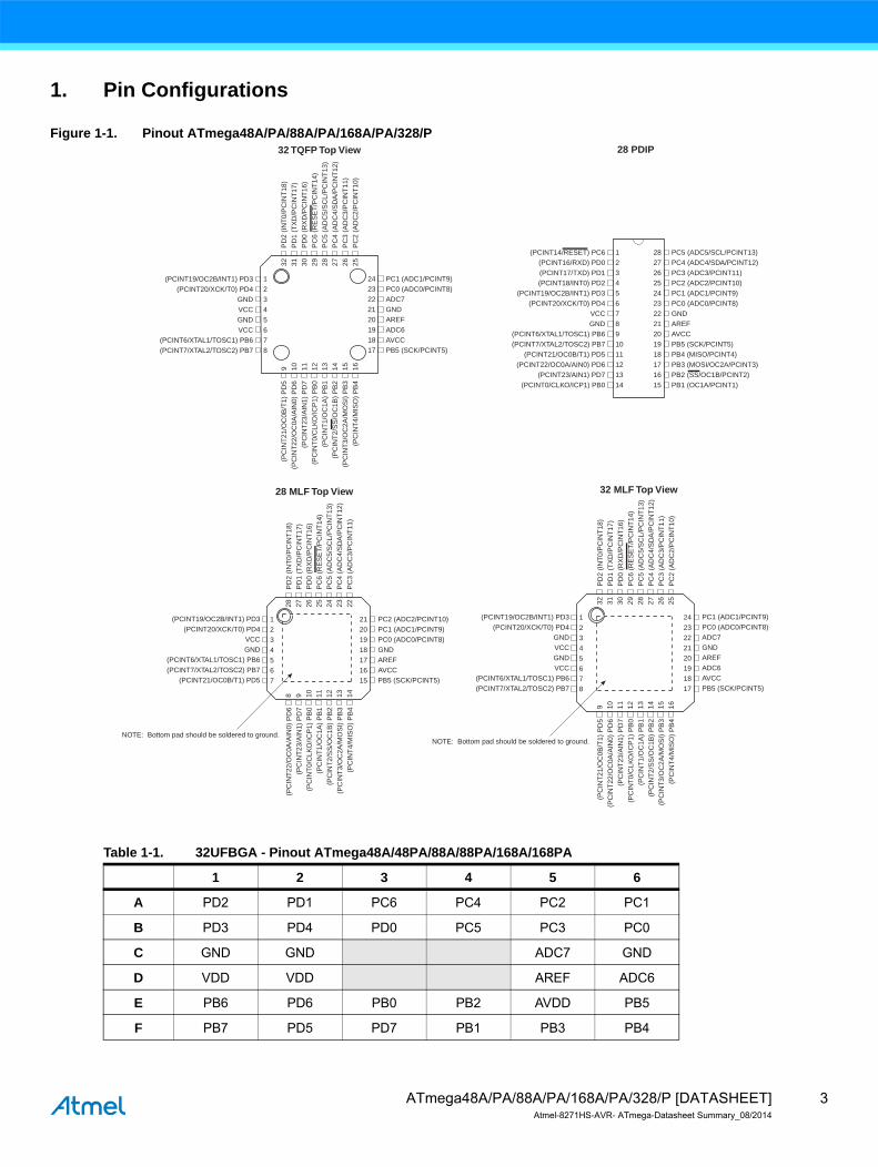
1. Pin Configurations
Figure 1-1. Pinout ATmega48A/PA/88A/PA/168A/PA/328/P
12345678
2423222120191817
(PCINT19/OC2B/INT1) PD3(PCINT20/XCK/T0) PD4
GNDVCCGNDVCC
(PCINT6/XTAL1/TOSC1) PB6(PCINT7/XTAL2/TOSC2) PB7
PC1 (ADC1/PCINT9)PC0 (ADC0/PCINT8)ADC7GNDAREFADC6AVCCPB5 (SCK/PCINT5)
32 31 30 29 28 27 26 25
9 10 11 12 13 14 15 16
(PC
INT
21/O
C0B
/T1)
PD
5(P
CIN
T22
/OC
0A/A
IN0)
PD
6(P
CIN
T23
/AIN
1) P
D7
(PC
INT
0/C
LKO
/ICP
1) P
B0
(PC
INT
1/O
C1A
) P
B1
(PC
INT
2/S
S/O
C1B
) P
B2
(PC
INT
3/O
C2A
/MO
SI)
PB
3(P
CIN
T4/
MIS
O)
PB
4
PD
2 (I
NT
0/P
CIN
T18
)P
D1
(TX
D/P
CIN
T17
)P
D0
(RX
D/P
CIN
T16
)P
C6
(RE
SE
T/P
CIN
T14
)P
C5
(AD
C5/
SC
L/P
CIN
T13
)P
C4
(AD
C4/
SD
A/P
CIN
T12
)P
C3
(AD
C3/
PC
INT
11)
PC
2 (A
DC
2/P
CIN
T10
)
32 TQFP Top View
1234567891011121314
2827262524232221201918171615
(PCINT14/RESET) PC6(PCINT16/RXD) PD0(PCINT17/TXD) PD1(PCINT18/INT0) PD2
(PCINT19/OC2B/INT1) PD3(PCINT20/XCK/T0) PD4
VCCGND
(PCINT6/XTAL1/TOSC1) PB6(PCINT7/XTAL2/TOSC2) PB7
(PCINT21/OC0B/T1) PD5(PCINT22/OC0A/AIN0) PD6
(PCINT23/AIN1) PD7(PCINT0/CLKO/ICP1) PB0
PC5 (ADC5/SCL/PCINT13)PC4 (ADC4/SDA/PCINT12)PC3 (ADC3/PCINT11)PC2 (ADC2/PCINT10)PC1 (ADC1/PCINT9)PC0 (ADC0/PCINT8)GNDAREFAVCCPB5 (SCK/PCINT5)PB4 (MISO/PCINT4)PB3 (MOSI/OC2A/PCINT3)PB2 (SS/OC1B/PCINT2)PB1 (OC1A/PCINT1)
28 PDIP
12345678
2423222120191817
32 31 30 29 28 27 26 25
9 10 11 12 13 14 15 16
32 MLF Top View
(PCINT19/OC2B/INT1) PD3(PCINT20/XCK/T0) PD4
GNDVCCGNDVCC
(PCINT6/XTAL1/TOSC1) PB6(PCINT7/XTAL2/TOSC2) PB7
PC1 (ADC1/PCINT9)PC0 (ADC0/PCINT8)ADC7GNDAREFADC6AVCCPB5 (SCK/PCINT5)
(PC
INT
21/O
C0B
/T1)
PD
5(P
CIN
T22
/OC
0A/A
IN0)
PD
6(P
CIN
T23
/AIN
1) P
D7
(PC
INT
0/C
LKO
/ICP
1) P
B0
(PC
INT
1/O
C1A
) P
B1
(PC
INT
2/S
S/O
C1B
) P
B2
(PC
INT
3/O
C2A
/MO
SI)
PB
3(P
CIN
T4/
MIS
O)
PB
4
PD
2 (I
NT
0/P
CIN
T18
)P
D1
(TX
D/P
CIN
T17
)P
D0
(RX
D/P
CIN
T16
)P
C6
(RE
SE
T/P
CIN
T14
)P
C5
(AD
C5/
SC
L/P
CIN
T13
)P
C4
(AD
C4/
SD
A/P
CIN
T12
)P
C3
(AD
C3/
PC
INT
11)
PC
2 (A
DC
2/P
CIN
T10
)
NOTE: Bottom pad should be soldered to ground.
1234567
21201918171615
28 27 26 25 24 23 22
8 9 10 11 12 13 14
28 MLF Top View
(PCINT19/OC2B/INT1) PD3(PCINT20/XCK/T0) PD4
VCCGND
(PCINT6/XTAL1/TOSC1) PB6(PCINT7/XTAL2/TOSC2) PB7
(PCINT21/OC0B/T1) PD5
(PC
INT
22/O
C0A
/AIN
0) P
D6
(PC
INT
23/A
IN1)
PD
7(P
CIN
T0/
CLK
O/IC
P1)
PB
0(P
CIN
T1/
OC
1A)
PB
1(P
CIN
T2/
SS
/OC
1B)
PB
2(P
CIN
T3/
OC
2A/M
OS
I) P
B3
(PC
INT
4/M
ISO
) P
B4
PD
2 (I
NT
0/P
CIN
T18
)P
D1
(TX
D/P
CIN
T17
)P
D0
(RX
D/P
CIN
T16
)P
C6
(RE
SE
T/P
CIN
T14
)P
C5
(AD
C5/
SC
L/P
CIN
T13
)P
C4
(AD
C4/
SD
A/P
CIN
T12
)P
C3
(AD
C3/
PC
INT
11)
PC2 (ADC2/PCINT10)PC1 (ADC1/PCINT9)PC0 (ADC0/PCINT8)GNDAREFAVCCPB5 (SCK/PCINT5)
NOTE: Bottom pad should be soldered to ground.
Table 1-1. 32UFBGA - Pinout ATmega48A/48PA/88A/88PA/168A/168PA
1 2 3 4 5 6
A PD2 PD1 PC6 PC4 PC2 PC1
B PD3 PD4 PD0 PC5 PC3 PC0
C GND GND ADC7 GND
D VDD VDD AREF ADC6
E PB6 PD6 PB0 PB2 AVDD PB5
F PB7 PD5 PD7 PB1 PB3 PB4
3ATmega48A/PA/88A/PA/168A/PA/328/P [DATASHEET]Atmel-8271HS-AVR- ATmega-Datasheet Summary_08/2014
1.1 Pin Descriptions
1.1.1 VCC
Digital supply voltage.
1.1.2 GND
Ground.
1.1.3 Port B (PB7:0) XTAL1/XTAL2/TOSC1/TOSC2
Port B is an 8-bit bi-directional I/O port with internal pull-up resistors (selected for each bit). The Port B output buffers have symmetrical drive characteristics with both high sink and source capability. As inputs, Port B pins that are externally pulled low will source current if the pull-up resistors are activated. The Port B pins are tri-stated when a reset condition becomes active, even if the clock is not running.
Depending on the clock selection fuse settings, PB6 can be used as input to the inverting Oscillator amplifier and input to the internal clock operating circuit.
Depending on the clock selection fuse settings, PB7 can be used as output from the inverting Oscillator amplifier.
If the Internal Calibrated RC Oscillator is used as chip clock source, PB7...6 is used as TOSC2...1 input for the Asynchronous Timer/Counter2 if the AS2 bit in ASSR is set.
The various special features of Port B are elaborated in ”Alternate Functions of Port B” on page 83 and ”System Clock and Clock Options” on page 27.
1.1.4 Port C (PC5:0)
Port C is a 7-bit bi-directional I/O port with internal pull-up resistors (selected for each bit). The PC5...0 output buffers have symmetrical drive characteristics with both high sink and source capability. As inputs, Port C pins that are externally pulled low will source current if the pull-up resistors are activated. The Port C pins are tri-stated when a reset condition becomes active, even if the clock is not running.
1.1.5 PC6/RESET
If the RSTDISBL Fuse is programmed, PC6 is used as an I/O pin. Note that the electrical characteristics of PC6 differ from those of the other pins of Port C.
If the RSTDISBL Fuse is unprogrammed, PC6 is used as a Reset input. A low level on this pin for longer than the minimum pulse length will generate a Reset, even if the clock is not running. The minimum pulse length is given in Table 29-16 on page 311. Shorter pulses are not guaranteed to generate a Reset.
The various special features of Port C are elaborated in ”Alternate Functions of Port C” on page 86.|
1.1.6 Port D (PD7:0)
Port D is an 8-bit bi-directional I/O port with internal pull-up resistors (selected for each bit). The Port D output buffers have symmetrical drive characteristics with both high sink and source capability. As inputs, Port D pins that are externally pulled low will source current if the pull-up resistors are activated. The Port D pins are tri-stated when a reset condition becomes active, even if the clock is not running.
The various special features of Port D are elaborated in ”Alternate Functions of Port D” on page 89.
4ATmega48A/PA/88A/PA/168A/PA/328/P [DATASHEET]Atmel-8271HS-AVR- ATmega-Datasheet Summary_08/2014
1.1.7 AVCC
AVCC is the supply voltage pin for the A/D Converter, PC3:0, and ADC7:6. It should be externally connected to VCC, even if the ADC is not used. If the ADC is used, it should be connected to VCC through a low-pass filter. Note that PC6...4 use digital supply voltage, VCC.
1.1.8 AREF
AREF is the analog reference pin for the A/D Converter.
1.1.9 ADC7:6 (TQFP and QFN/MLF Package Only)
In the TQFP and QFN/MLF package, ADC7:6 serve as analog inputs to the A/D converter. These pins are powered from the analog supply and serve as 10-bit ADC channels.
5ATmega48A/PA/88A/PA/168A/PA/328/P [DATASHEET]Atmel-8271HS-AVR- ATmega-Datasheet Summary_08/2014
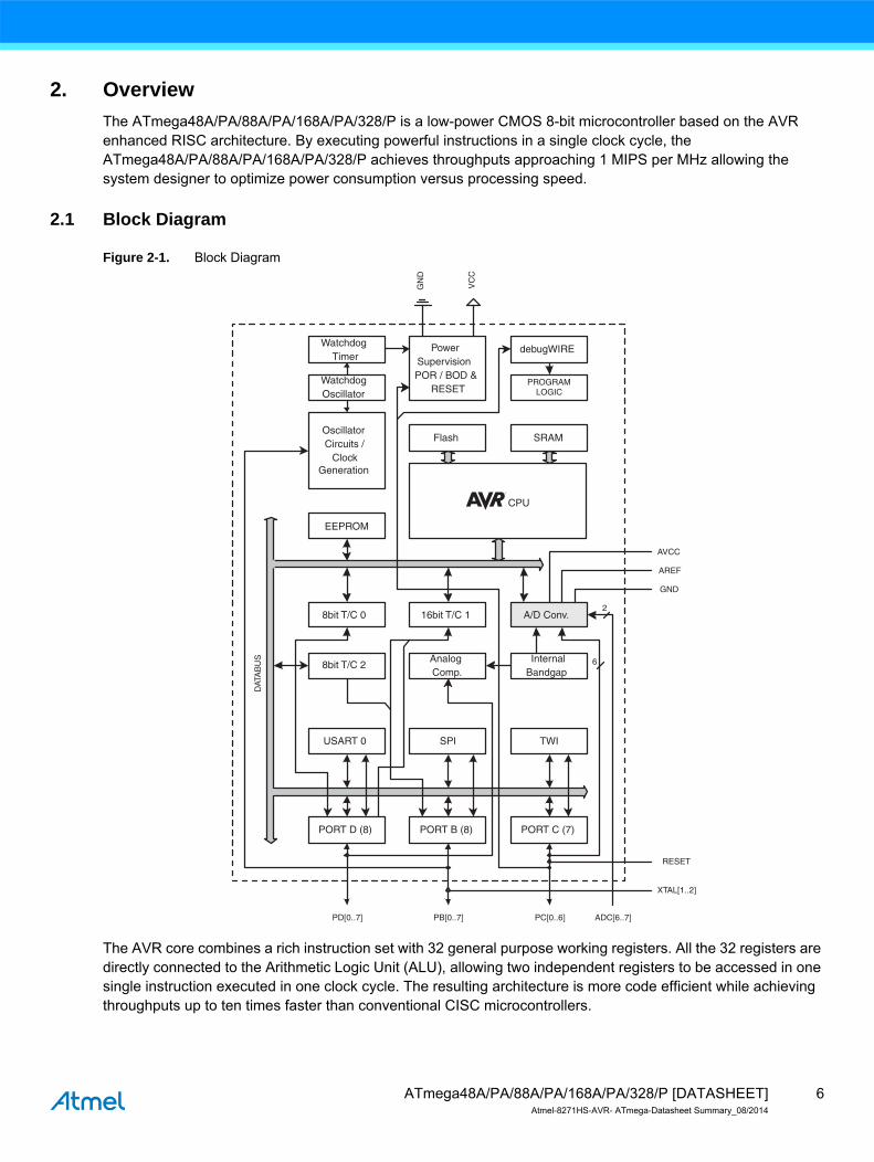
2. Overview
The ATmega48A/PA/88A/PA/168A/PA/328/P is a low-power CMOS 8-bit microcontroller based on the AVR enhanced RISC architecture. By executing powerful instructions in a single clock cycle, the ATmega48A/PA/88A/PA/168A/PA/328/P achieves throughputs approaching 1 MIPS per MHz allowing the system designer to optimize power consumption versus processing speed.
2.1 Block Diagram
Figure 2-1. Block Diagram
The AVR core combines a rich instruction set with 32 general purpose working registers. All the 32 registers are directly connected to the Arithmetic Logic Unit (ALU), allowing two independent registers to be accessed in one single instruction executed in one clock cycle. The resulting architecture is more code efficient while achieving throughputs up to ten times faster than conventional CISC microcontrollers.
PORT C (7)PORT B (8)PORT D (8)
USART 0
8bit T/C 2
16bit T/C 18bit T/C 0 A/D Conv.
InternalBandgap
AnalogComp.
SPI TWI
SRAMFlash
EEPROM
WatchdogOscillator
WatchdogTimer
OscillatorCircuits /
ClockGeneration
PowerSupervisionPOR / BOD &
RESET
VC
C
GN
D
PROGRAMLOGIC
debugWIRE
2
GND
AREF
AVCC
DAT
AB
US
ADC[6..7]PC[0..6]PB[0..7]PD[0..7]
6
RESET
XTAL[1..2]
CPU
6ATmega48A/PA/88A/PA/168A/PA/328/P [DATASHEET]Atmel-8271HS-AVR- ATmega-Datasheet Summary_08/2014
The ATmega48A/PA/88A/PA/168A/PA/328/P provides the following features: 4K/8Kbytes of In-System Programmable Flash with Read-While-Write capabilities, 256/512/512/1Kbytes EEPROM, 512/1K/1K/2Kbytes SRAM, 23 general purpose I/O lines, 32 general purpose working registers, three flexible Timer/Counters with compare modes, internal and external interrupts, a serial programmable USART, a byte-oriented 2-wire Serial Interface, an SPI serial port, a 6-channel 10-bit ADC (8 channels in TQFP and QFN/MLF packages), a programmable Watchdog Timer with internal Oscillator, and five software selectable power saving modes. The Idle mode stops the CPU while allowing the SRAM, Timer/Counters, USART, 2-wire Serial Interface, SPI port, and interrupt system to continue functioning. The Power-down mode saves the register contents but freezes the Oscillator, disabling all other chip functions until the next interrupt or hardware reset. In Power-save mode, the asynchronous timer continues to run, allowing the user to maintain a timer base while the rest of the device is sleeping. The ADC Noise Reduction mode stops the CPU and all I/O modules except asynchronous timer and ADC, to minimize switching noise during ADC conversions. In Standby mode, the crystal/resonator Oscillator is running while the rest of the device is sleeping. This allows very fast start-up combined with low power consumption.
Atmel® offers the QTouch® library for embedding capacitive touch buttons, sliders and wheels functionality into AVR® microcontrollers. The patented charge-transfer signal acquisition offers robust sensing and includes fully debounced reporting of touch keys and includes Adjacent Key Suppression® (AKS™) technology for unambiguous detection of key events. The easy-to-use QTouch Suite toolchain allows you to explore, develop and debug your own touch applications.
The device is manufactured using Atmel’s high density non-volatile memory technology. The On-chip ISP Flash allows the program memory to be reprogrammed In-System through an SPI serial interface, by a conventional non-volatile memory programmer, or by an On-chip Boot program running on the AVR core. The Boot program can use any interface to download the application program in the Application Flash memory. Software in the Boot Flash section will continue to run while the Application Flash section is updated, providing true Read-While-Write operation. By combining an 8-bit RISC CPU with In-System Self-Programmable Flash on a monolithic chip, the Atmel ATmega48A/PA/88A/PA/168A/PA/328/P is a powerful microcontroller that provides a highly flexible and cost effective solution to many embedded control applications.
The ATmega48A/PA/88A/PA/168A/PA/328/P AVR is supported with a full suite of program and system development tools including: C Compilers, Macro Assemblers, Program Debugger/Simulators, In-Circuit Emulators, and Evaluation kits.
2.2 Comparison Between Processors
The ATmega48A/PA/88A/PA/168A/PA/328/P differ only in memory sizes, boot loader support, and interrupt vector sizes. Table 2-1 summarizes the different memory and interrupt vector sizes for the devices.
Table 2-1. Memory Size Summary
Device Flash EEPROM RAM Interrupt Vector Size
ATmega48A 4KBytes 256Bytes 512Bytes 1 instruction word/vector
ATmega48PA 4KBytes 256Bytes 512Bytes 1 instruction word/vector
ATmega88A 8KBytes 512Bytes 1KBytes 1 instruction word/vector
ATmega88PA 8KBytes 512Bytes 1KBytes 1 instruction word/vector
ATmega168A 16KBytes 512Bytes 1KBytes 2 instruction words/vector
ATmega168PA 16KBytes 512Bytes 1KBytes 2 instruction words/vector
ATmega328 32KBytes 1KBytes 2KBytes 2 instruction words/vector
ATmega328P 32KBytes 1KBytes 2KBytes 2 instruction words/vector
7ATmega48A/PA/88A/PA/168A/PA/328/P [DATASHEET]Atmel-8271HS-AVR- ATmega-Datasheet Summary_08/2014
ATmega48A/PA/88A/PA/168A/PA/328/P support a real Read-While-Write Self-Programming mechanism. There is a separate Boot Loader Section, and the SPM instruction can only execute from there. In ATmega 48A/48PA there is no Read-While-Write support and no separate Boot Loader Section. The SPM instruction can execute from the entire Flash
3. Resources
A comprehensive set of development tools, application notes and datasheets are available for download on http://www.atmel.com/avr.
Note: 1.
4. Data Retention
Reliability Qualification results show that the projected data retention failure rate is much less than 1 PPM over 20 years at 85°C or 100 years at 25°C.
5. About Code Examples
This documentation contains simple code examples that briefly show how to use various parts of the device. These code examples assume that the part specific header file is included before compilation. Be aware that not all C compiler vendors include bit definitions in the header files and interrupt handling in C is compiler dependent. Please confirm with the C compiler documentation for more details.
For I/O Registers located in extended I/O map, “IN”, “OUT”, “SBIS”, “SBIC”, “CBI”, and “SBI” instructions must be replaced with instructions that allow access to extended I/O. Typically “LDS” and “STS” combined with “SBRS”, “SBRC”, “SBR”, and “CBR”.
6. Capacitive Touch Sensing
The Atmel® QTouch® Library provides a simple to use solution to realize touch sensitive interfaces on most Atmel AVR® microcontrollers. The QTouch Library includes support for the Atmel QTouch and Atmel QMatrix® acquisition methods.
Touch sensing can be added to any application by linking the appropriate Atmel QTouch Library for the AVR Microcontroller. This is done by using a simple set of APIs to define the touch channels and sensors, and then calling the touch sensing APIs to retrieve the channel information and determine the touch sensor states.
The QTouch Library is FREE and downloadable from the Atmel website at the following location: www.atmel.com/qtouchlibrary. For implementation details and other information, refer to the Atmel QTouch Library User Guide - also available for download from Atmel website.
8ATmega48A/PA/88A/PA/168A/PA/328/P [DATASHEET]Atmel-8271HS-AVR- ATmega-Datasheet Summary_08/2014
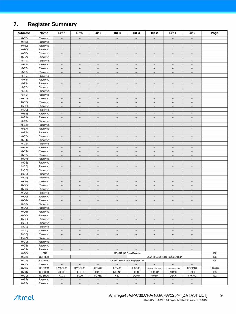
7. Register Summary
Address Name Bit 7 Bit 6 Bit 5 Bit 4 Bit 3 Bit 2 Bit 1 Bit 0 Page
(0xFF) Reserved – – – – – – – –
(0xFE) Reserved – – – – – – – –
(0xFD) Reserved – – – – – – – –
(0xFC) Reserved – – – – – – – –
(0xFB) Reserved – – – – – – – –
(0xFA) Reserved – – – – – – – –
(0xF9) Reserved – – – – – – – –
(0xF8) Reserved – – – – – – – –
(0xF7) Reserved – – – – – – – –
(0xF6) Reserved – – – – – – – –
(0xF5) Reserved – – – – – – – –
(0xF4) Reserved – – – – – – – –
(0xF3) Reserved – – – – – – – –
(0xF2) Reserved – – – – – – – –
(0xF1) Reserved – – – – – – – –
(0xF0) Reserved – – – – – – – –
(0xEF) Reserved – – – – – – – –
(0xEE) Reserved – – – – – – – –
(0xED) Reserved – – – – – – – –
(0xEC) Reserved – – – – – – – –
(0xEB) Reserved – – – – – – – –
(0xEA) Reserved – – – – – – – –
(0xE9) Reserved – – – – – – – –
(0xE8) Reserved – – – – – – – –
(0xE7) Reserved – – – – – – – –
(0xE6) Reserved – – – – – – – –
(0xE5) Reserved – – – – – – – –
(0xE4) Reserved – – – – – – – –
(0xE3) Reserved – – – – – – – –
(0xE2) Reserved – – – – – – – –
(0xE1) Reserved – – – – – – – –
(0xE0) Reserved – – – – – – – –
(0xDF) Reserved – – – – – – – –
(0xDE) Reserved – – – – – – – –
(0xDD) Reserved – – – – – – – –
(0xDC) Reserved – – – – – – – –
(0xDB) Reserved – – – – – – – –
(0xDA) Reserved – – – – – – – –
(0xD9) Reserved – – – – – – – –
(0xD8) Reserved – – – – – – – –
(0xD7) Reserved – – – – – – – –
(0xD6) Reserved – – – – – – – –
(0xD5) Reserved – – – – – – – –
(0xD4) Reserved – – – – – – – –
(0xD3) Reserved – – – – – – – –
(0xD2) Reserved – – – – – – – –
(0xD1) Reserved – – – – – – – –
(0xD0) Reserved – – – – – – – –
(0xCF) Reserved – – – – – – – –
(0xCE) Reserved – – – – – – – –
(0xCD) Reserved – – – – – – – –
(0xCC) Reserved – – – – – – – –
(0xCB) Reserved – – – – – – – –
(0xCA) Reserved – – – – – – – –
(0xC9) Reserved – – – – – – – –
(0xC8) Reserved – – – – – – – –
(0xC7) Reserved – – – – – – – –
(0xC6) UDR0 USART I/O Data Register 192
(0xC5) UBRR0H USART Baud Rate Register High 196
(0xC4) UBRR0L USART Baud Rate Register Low 196
(0xC3) Reserved – – – – – – – –
(0xC2) UCSR0C UMSEL01 UMSEL00 UPM01 UPM00 USBS0 UCSZ01 /UDORD0 UCSZ00 / UCPHA0 UCPOL0 194/205
(0xC1) UCSR0B RXCIE0 TXCIE0 UDRIE0 RXEN0 TXEN0 UCSZ02 RXB80 TXB80 193
(0xC0) UCSR0A RXC0 TXC0 UDRE0 FE0 DOR0 UPE0 U2X0 MPCM0 192
(0xBF) Reserved – – – – – – – –
(0xBE) Reserved – – – – – – – –
9ATmega48A/PA/88A/PA/168A/PA/328/P [DATASHEET]Atmel-8271HS-AVR- ATmega-Datasheet Summary_08/2014
(0xBD) TWAMR TWAM6 TWAM5 TWAM4 TWAM3 TWAM2 TWAM1 TWAM0 – 235
(0xBC) TWCR TWINT TWEA TWSTA TWSTO TWWC TWEN – TWIE 232
(0xBB) TWDR 2-wire Serial Interface Data Register 234
(0xBA) TWAR TWA6 TWA5 TWA4 TWA3 TWA2 TWA1 TWA0 TWGCE 234
(0xB9) TWSR TWS7 TWS6 TWS5 TWS4 TWS3 – TWPS1 TWPS0 233
(0xB8) TWBR 2-wire Serial Interface Bit Rate Register 232
(0xB7) Reserved – – – – – – –
(0xB6) ASSR – EXCLK AS2 TCN2UB OCR2AUB OCR2BUB TCR2AUB TCR2BUB 159
(0xB5) Reserved – – – – – – – –
(0xB4) OCR2B Timer/Counter2 Output Compare Register B 158
(0xB3) OCR2A Timer/Counter2 Output Compare Register A 158
(0xB2) TCNT2 Timer/Counter2 (8-bit) 158
(0xB1) TCCR2B FOC2A FOC2B – – WGM22 CS22 CS21 CS20 157
(0xB0) TCCR2A COM2A1 COM2A0 COM2B1 COM2B0 – – WGM21 WGM20 154
(0xAF) Reserved – – – – – – – –
(0xAE) Reserved – – – – – – – –
(0xAD) Reserved – – – – – – – –
(0xAC) Reserved – – – – – – – –
(0xAB) Reserved – – – – – – – –
(0xAA) Reserved – – – – – – – –
(0xA9) Reserved – – – – – – – –
(0xA8) Reserved – – – – – – – –
(0xA7) Reserved – – – – – – – –
(0xA6) Reserved – – – – – – – –
(0xA5) Reserved – – – – – – – –
(0xA4) Reserved – – – – – – – –
(0xA3) Reserved – – – – – – – –
(0xA2) Reserved – – – – – – – –
(0xA1) Reserved – – – – – – – –
(0xA0) Reserved – – – – – – – –
(0x9F) Reserved – – – – – – – –
(0x9E) Reserved – – – – – – – –
(0x9D) Reserved – – – – – – – –
(0x9C) Reserved – – – – – – – –
(0x9B) Reserved – – – – – – – –
(0x9A) Reserved – – – – – – – –
(0x99) Reserved – – – – – – – –
(0x98) Reserved – – – – – – – –
(0x97) Reserved – – – – – – – –
(0x96) Reserved – – – – – – – –
(0x95) Reserved – – – – – – – –
(0x94) Reserved – – – – – – – –
(0x93) Reserved – – – – – – – –
(0x92) Reserved – – – – – – – –
(0x91) Reserved – – – – – – – –
(0x90) Reserved – – – – – – – –
(0x8F) Reserved – – – – – – – –
(0x8E) Reserved – – – – – – – –
(0x8D) Reserved – – – – – – – –
(0x8C) Reserved – – – – – – – –
(0x8B) OCR1BH Timer/Counter1 - Output Compare Register B High Byte 136
(0x8A) OCR1BL Timer/Counter1 - Output Compare Register B Low Byte 136
(0x89) OCR1AH Timer/Counter1 - Output Compare Register A High Byte 136
(0x88) OCR1AL Timer/Counter1 - Output Compare Register A Low Byte 136
(0x87) ICR1H Timer/Counter1 - Input Capture Register High Byte 136
(0x86) ICR1L Timer/Counter1 - Input Capture Register Low Byte 136
(0x85) TCNT1H Timer/Counter1 - Counter Register High Byte 135
(0x84) TCNT1L Timer/Counter1 - Counter Register Low Byte 135
(0x83) Reserved – – – – – – – –
(0x82) TCCR1C FOC1A FOC1B – – – – – – 135
(0x81) TCCR1B ICNC1 ICES1 – WGM13 WGM12 CS12 CS11 CS10 134
(0x80) TCCR1A COM1A1 COM1A0 COM1B1 COM1B0 – – WGM11 WGM10 132
(0x7F) DIDR1 – – – – – – AIN1D AIN0D 238
(0x7E) DIDR0 – – ADC5D ADC4D ADC3D ADC2D ADC1D ADC0D 253
(0x7D) Reserved – – – – – – – –
(0x7C) ADMUX REFS1 REFS0 ADLAR – MUX3 MUX2 MUX1 MUX0 250
(0x7B) ADCSRB – ACME – – – ADTS2 ADTS1 ADTS0 253
(0x7A) ADCSRA ADEN ADSC ADATE ADIF ADIE ADPS2 ADPS1 ADPS0 251
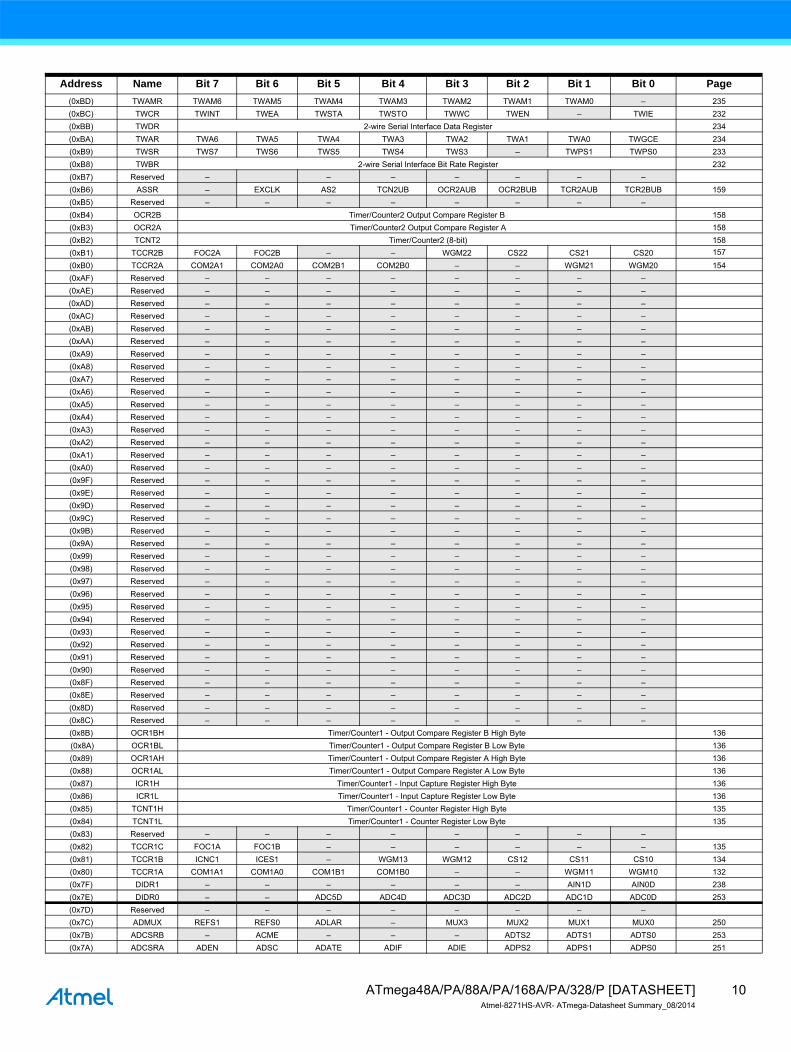
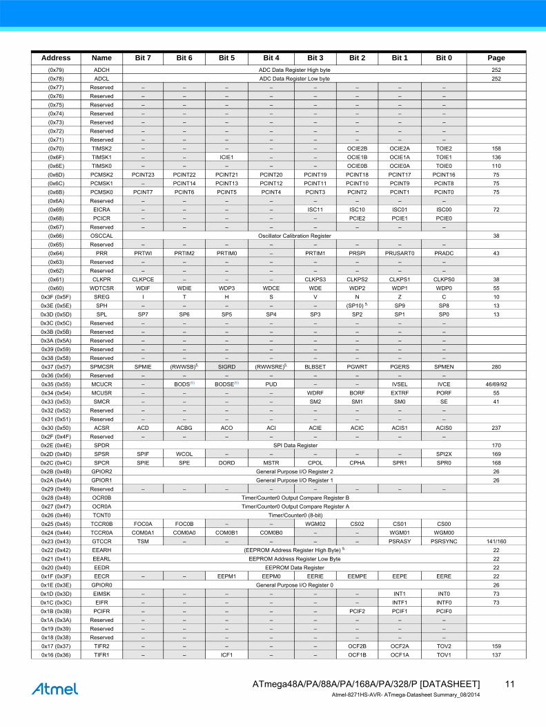
Address Name Bit 7 Bit 6 Bit 5 Bit 4 Bit 3 Bit 2 Bit 1 Bit 0 Page
10ATmega48A/PA/88A/PA/168A/PA/328/P [DATASHEET]Atmel-8271HS-AVR- ATmega-Datasheet Summary_08/2014
(0x79) ADCH ADC Data Register High byte 252
(0x78) ADCL ADC Data Register Low byte 252
(0x77) Reserved – – – – – – – –
(0x76) Reserved – – – – – – – –
(0x75) Reserved – – – – – – – –
(0x74) Reserved – – – – – – – –
(0x73) Reserved – – – – – – – –
(0x72) Reserved – – – – – – – –
(0x71) Reserved – – – – – – – –
(0x70) TIMSK2 – – – – – OCIE2B OCIE2A TOIE2 158
(0x6F) TIMSK1 – – ICIE1 – – OCIE1B OCIE1A TOIE1 136
(0x6E) TIMSK0 – – – – – OCIE0B OCIE0A TOIE0 110
(0x6D) PCMSK2 PCINT23 PCINT22 PCINT21 PCINT20 PCINT19 PCINT18 PCINT17 PCINT16 75
(0x6C) PCMSK1 – PCINT14 PCINT13 PCINT12 PCINT11 PCINT10 PCINT9 PCINT8 75
(0x6B) PCMSK0 PCINT7 PCINT6 PCINT5 PCINT4 PCINT3 PCINT2 PCINT1 PCINT0 75
(0x6A) Reserved – – – – – – – –
(0x69) EICRA – – – – ISC11 ISC10 ISC01 ISC00 72
(0x68) PCICR – – – – – PCIE2 PCIE1 PCIE0
(0x67) Reserved – – – – – – – –
(0x66) OSCCAL Oscillator Calibration Register 38
(0x65) Reserved – – – – – – – –
(0x64) PRR PRTWI PRTIM2 PRTIM0 – PRTIM1 PRSPI PRUSART0 PRADC 43
(0x63) Reserved – – – – – – – –
(0x62) Reserved – – – – – – – –
(0x61) CLKPR CLKPCE – – – CLKPS3 CLKPS2 CLKPS1 CLKPS0 38
(0x60) WDTCSR WDIF WDIE WDP3 WDCE WDE WDP2 WDP1 WDP0 55
0x3F (0x5F) SREG I T H S V N Z C 10
0x3E (0x5E) SPH – – – – – (SP10) 5. SP9 SP8 13
0x3D (0x5D) SPL SP7 SP6 SP5 SP4 SP3 SP2 SP1 SP0 13
0x3C (0x5C) Reserved – – – – – – – –
0x3B (0x5B) Reserved – – – – – – – –
0x3A (0x5A) Reserved – – – – – – – –
0x39 (0x59) Reserved – – – – – – – –
0x38 (0x58) Reserved – – – – – – – –
0x37 (0x57) SPMCSR SPMIE (RWWSB)5. SIGRD (RWWSRE)5. BLBSET PGWRT PGERS SPMEN 280
0x36 (0x56) Reserved – – – – – – – –
0x35 (0x55) MCUCR – BODS(6) BODSE(6) PUD – – IVSEL IVCE 46/69/92
0x34 (0x54) MCUSR – – – – WDRF BORF EXTRF PORF 55
0x33 (0x53) SMCR – – – – SM2 SM1 SM0 SE 41
0x32 (0x52) Reserved – – – – – – – –
0x31 (0x51) Reserved – – – – – – – –
0x30 (0x50) ACSR ACD ACBG ACO ACI ACIE ACIC ACIS1 ACIS0 237
0x2F (0x4F) Reserved – – – – – – – –
0x2E (0x4E) SPDR SPI Data Register 170
0x2D (0x4D) SPSR SPIF WCOL – – – – – SPI2X 169
0x2C (0x4C) SPCR SPIE SPE DORD MSTR CPOL CPHA SPR1 SPR0 168
0x2B (0x4B) GPIOR2 General Purpose I/O Register 2 26
0x2A (0x4A) GPIOR1 General Purpose I/O Register 1 26
0x29 (0x49) Reserved – – – – – – – –
0x28 (0x48) OCR0B Timer/Counter0 Output Compare Register B
0x27 (0x47) OCR0A Timer/Counter0 Output Compare Register A
0x26 (0x46) TCNT0 Timer/Counter0 (8-bit)
0x25 (0x45) TCCR0B FOC0A FOC0B – – WGM02 CS02 CS01 CS00
0x24 (0x44) TCCR0A COM0A1 COM0A0 COM0B1 COM0B0 – – WGM01 WGM00
0x23 (0x43) GTCCR TSM – – – – – PSRASY PSRSYNC 141/160
0x22 (0x42) EEARH (EEPROM Address Register High Byte) 5. 22
0x21 (0x41) EEARL EEPROM Address Register Low Byte 22
0x20 (0x40) EEDR EEPROM Data Register 22
0x1F (0x3F) EECR – – EEPM1 EEPM0 EERIE EEMPE EEPE EERE 22
0x1E (0x3E) GPIOR0 General Purpose I/O Register 0 26
0x1D (0x3D) EIMSK – – – – – – INT1 INT0 73
0x1C (0x3C) EIFR – – – – – – INTF1 INTF0 73
0x1B (0x3B) PCIFR – – – – – PCIF2 PCIF1 PCIF0
0x1A (0x3A) Reserved – – – – – – – –
0x19 (0x39) Reserved – – – – – – – –
0x18 (0x38) Reserved – – – – – – – –
0x17 (0x37) TIFR2 – – – – – OCF2B OCF2A TOV2 159
0x16 (0x36) TIFR1 – – ICF1 – – OCF1B OCF1A TOV1 137
Address Name Bit 7 Bit 6 Bit 5 Bit 4 Bit 3 Bit 2 Bit 1 Bit 0 Page
11ATmega48A/PA/88A/PA/168A/PA/328/P [DATASHEET]Atmel-8271HS-AVR- ATmega-Datasheet Summary_08/2014
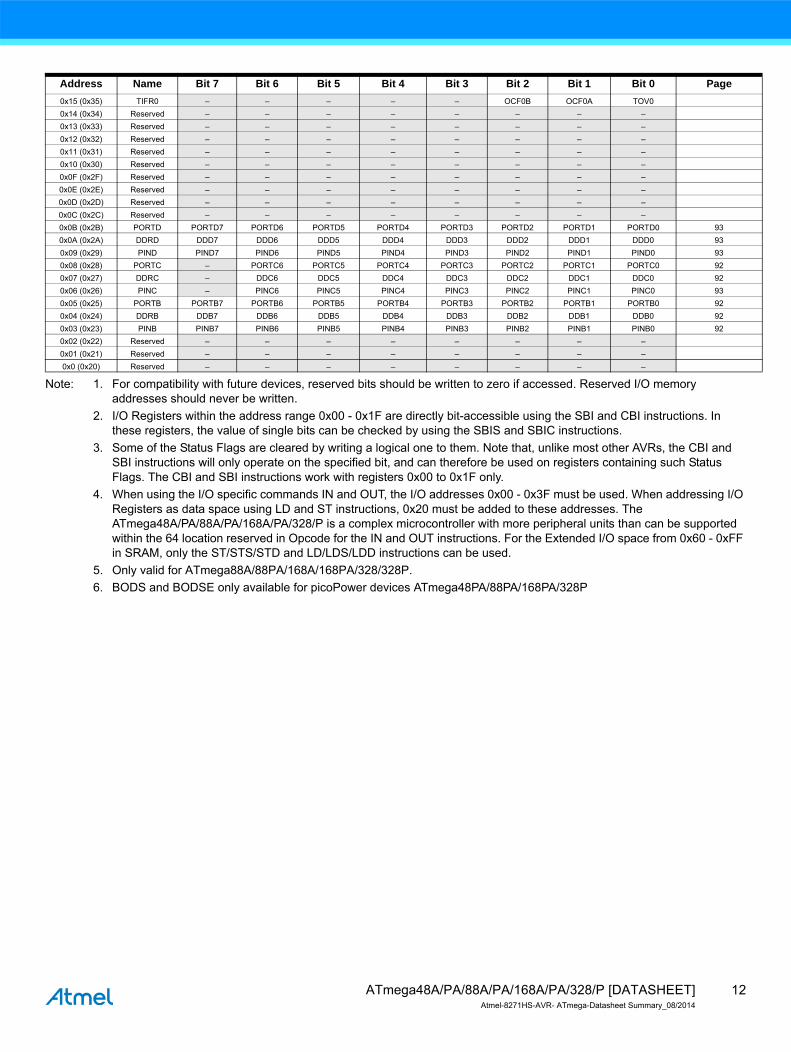
Note: 1. For compatibility with future devices, reserved bits should be written to zero if accessed. Reserved I/O memory addresses should never be written.
2. I/O Registers within the address range 0x00 - 0x1F are directly bit-accessible using the SBI and CBI instructions. In these registers, the value of single bits can be checked by using the SBIS and SBIC instructions.
3. Some of the Status Flags are cleared by writing a logical one to them. Note that, unlike most other AVRs, the CBI and SBI instructions will only operate on the specified bit, and can therefore be used on registers containing such Status Flags. The CBI and SBI instructions work with registers 0x00 to 0x1F only.
4. When using the I/O specific commands IN and OUT, the I/O addresses 0x00 - 0x3F must be used. When addressing I/O Registers as data space using LD and ST instructions, 0x20 must be added to these addresses. The ATmega48A/PA/88A/PA/168A/PA/328/P is a complex microcontroller with more peripheral units than can be supported within the 64 location reserved in Opcode for the IN and OUT instructions. For the Extended I/O space from 0x60 - 0xFF in SRAM, only the ST/STS/STD and LD/LDS/LDD instructions can be used.
5. Only valid for ATmega88A/88PA/168A/168PA/328/328P.
6. BODS and BODSE only available for picoPower devices ATmega48PA/88PA/168PA/328P
0x15 (0x35) TIFR0 – – – – – OCF0B OCF0A TOV0
0x14 (0x34) Reserved – – – – – – – –
0x13 (0x33) Reserved – – – – – – – –
0x12 (0x32) Reserved – – – – – – – –
0x11 (0x31) Reserved – – – – – – – –
0x10 (0x30) Reserved – – – – – – – –
0x0F (0x2F) Reserved – – – – – – – –
0x0E (0x2E) Reserved – – – – – – – –
0x0D (0x2D) Reserved – – – – – – – –
0x0C (0x2C) Reserved – – – – – – – –
0x0B (0x2B) PORTD PORTD7 PORTD6 PORTD5 PORTD4 PORTD3 PORTD2 PORTD1 PORTD0 93
0x0A (0x2A) DDRD DDD7 DDD6 DDD5 DDD4 DDD3 DDD2 DDD1 DDD0 93
0x09 (0x29) PIND PIND7 PIND6 PIND5 PIND4 PIND3 PIND2 PIND1 PIND0 93
0x08 (0x28) PORTC – PORTC6 PORTC5 PORTC4 PORTC3 PORTC2 PORTC1 PORTC0 92
0x07 (0x27) DDRC – DDC6 DDC5 DDC4 DDC3 DDC2 DDC1 DDC0 92
0x06 (0x26) PINC – PINC6 PINC5 PINC4 PINC3 PINC2 PINC1 PINC0 93
0x05 (0x25) PORTB PORTB7 PORTB6 PORTB5 PORTB4 PORTB3 PORTB2 PORTB1 PORTB0 92
0x04 (0x24) DDRB DDB7 DDB6 DDB5 DDB4 DDB3 DDB2 DDB1 DDB0 92
0x03 (0x23) PINB PINB7 PINB6 PINB5 PINB4 PINB3 PINB2 PINB1 PINB0 92
0x02 (0x22) Reserved – – – – – – – –
0x01 (0x21) Reserved – – – – – – – –
0x0 (0x20) Reserved – – – – – – – –
Address Name Bit 7 Bit 6 Bit 5 Bit 4 Bit 3 Bit 2 Bit 1 Bit 0 Page
12ATmega48A/PA/88A/PA/168A/PA/328/P [DATASHEET]Atmel-8271HS-AVR- ATmega-Datasheet Summary_08/2014
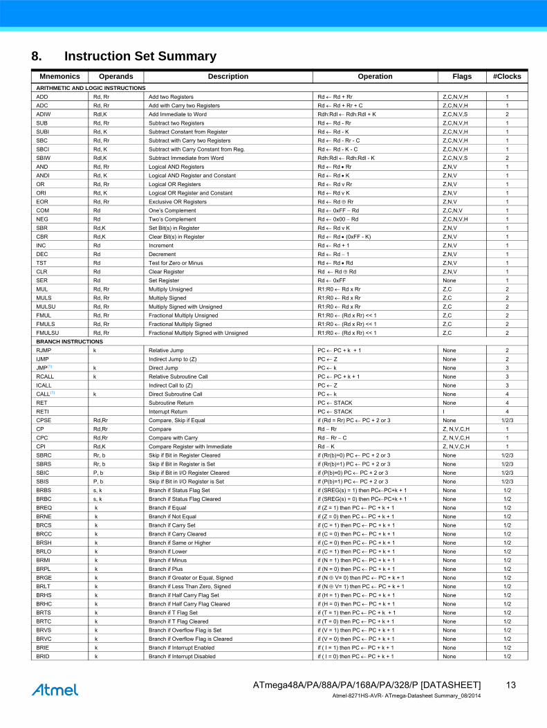
8. Instruction Set Summary
Mnemonics Operands Description Operation Flags #Clocks
ARITHMETIC AND LOGIC INSTRUCTIONS
ADD Rd, Rr Add two Registers Rd Rd + Rr Z,C,N,V,H 1
ADC Rd, Rr Add with Carry two Registers Rd Rd + Rr + C Z,C,N,V,H 1
ADIW Rdl,K Add Immediate to Word Rdh:Rdl Rdh:Rdl + K Z,C,N,V,S 2
SUB Rd, Rr Subtract two Registers Rd Rd - Rr Z,C,N,V,H 1
SUBI Rd, K Subtract Constant from Register Rd Rd - K Z,C,N,V,H 1
SBC Rd, Rr Subtract with Carry two Registers Rd Rd - Rr - C Z,C,N,V,H 1
SBCI Rd, K Subtract with Carry Constant from Reg. Rd Rd - K - C Z,C,N,V,H 1
SBIW Rdl,K Subtract Immediate from Word Rdh:Rdl Rdh:Rdl - K Z,C,N,V,S 2
AND Rd, Rr Logical AND Registers Rd Rd Rr Z,N,V 1
ANDI Rd, K Logical AND Register and Constant Rd Rd K Z,N,V 1
OR Rd, Rr Logical OR Registers Rd Rd v Rr Z,N,V 1
ORI Rd, K Logical OR Register and Constant Rd Rd v K Z,N,V 1
EOR Rd, Rr Exclusive OR Registers Rd Rd Rr Z,N,V 1
COM Rd One’s Complement Rd 0xFF Rd Z,C,N,V 1
NEG Rd Two’s Complement Rd 0x00 Rd Z,C,N,V,H 1
SBR Rd,K Set Bit(s) in Register Rd Rd v K Z,N,V 1
CBR Rd,K Clear Bit(s) in Register Rd Rd (0xFF - K) Z,N,V 1
INC Rd Increment Rd Rd + 1 Z,N,V 1
DEC Rd Decrement Rd Rd 1 Z,N,V 1
TST Rd Test for Zero or Minus Rd Rd Rd Z,N,V 1
CLR Rd Clear Register Rd Rd Rd Z,N,V 1
SER Rd Set Register Rd 0xFF None 1
MUL Rd, Rr Multiply Unsigned R1:R0 Rd x Rr Z,C 2
MULS Rd, Rr Multiply Signed R1:R0 Rd x Rr Z,C 2
MULSU Rd, Rr Multiply Signed with Unsigned R1:R0 Rd x Rr Z,C 2
FMUL Rd, Rr Fractional Multiply Unsigned R1:R0 (Rd x Rr) << 1 Z,C 2
FMULS Rd, Rr Fractional Multiply Signed R1:R0 (Rd x Rr) << 1 Z,C 2
FMULSU Rd, Rr Fractional Multiply Signed with Unsigned R1:R0 (Rd x Rr) << 1 Z,C 2
BRANCH INSTRUCTIONS
RJMP k Relative Jump PC PC + k + 1 None 2
IJMP Indirect Jump to (Z) PC Z None 2
JMP(1) k Direct Jump PC k None 3
RCALL k Relative Subroutine Call PC PC + k + 1 None 3
ICALL Indirect Call to (Z) PC Z None 3
CALL(1) k Direct Subroutine Call PC k None 4
RET Subroutine Return PC STACK None 4
RETI Interrupt Return PC STACK I 4
CPSE Rd,Rr Compare, Skip if Equal if (Rd = Rr) PC PC + 2 or 3 None 1/2/3
CP Rd,Rr Compare Rd Rr Z, N,V,C,H 1
CPC Rd,Rr Compare with Carry Rd Rr C Z, N,V,C,H 1
CPI Rd,K Compare Register with Immediate Rd K Z, N,V,C,H 1
SBRC Rr, b Skip if Bit in Register Cleared if (Rr(b)=0) PC PC + 2 or 3 None 1/2/3
SBRS Rr, b Skip if Bit in Register is Set if (Rr(b)=1) PC PC + 2 or 3 None 1/2/3
SBIC P, b Skip if Bit in I/O Register Cleared if (P(b)=0) PC PC + 2 or 3 None 1/2/3
SBIS P, b Skip if Bit in I/O Register is Set if (P(b)=1) PC PC + 2 or 3 None 1/2/3
BRBS s, k Branch if Status Flag Set if (SREG(s) = 1) then PCPC+k + 1 None 1/2
BRBC s, k Branch if Status Flag Cleared if (SREG(s) = 0) then PCPC+k + 1 None 1/2
BREQ k Branch if Equal if (Z = 1) then PC PC + k + 1 None 1/2
BRNE k Branch if Not Equal if (Z = 0) then PC PC + k + 1 None 1/2
BRCS k Branch if Carry Set if (C = 1) then PC PC + k + 1 None 1/2
BRCC k Branch if Carry Cleared if (C = 0) then PC PC + k + 1 None 1/2
BRSH k Branch if Same or Higher if (C = 0) then PC PC + k + 1 None 1/2
BRLO k Branch if Lower if (C = 1) then PC PC + k + 1 None 1/2
BRMI k Branch if Minus if (N = 1) then PC PC + k + 1 None 1/2
BRPL k Branch if Plus if (N = 0) then PC PC + k + 1 None 1/2
BRGE k Branch if Greater or Equal, Signed if (N V= 0) then PC PC + k + 1 None 1/2
BRLT k Branch if Less Than Zero, Signed if (N V= 1) then PC PC + k + 1 None 1/2
BRHS k Branch if Half Carry Flag Set if (H = 1) then PC PC + k + 1 None 1/2
BRHC k Branch if Half Carry Flag Cleared if (H = 0) then PC PC + k + 1 None 1/2
BRTS k Branch if T Flag Set if (T = 1) then PC PC + k + 1 None 1/2
BRTC k Branch if T Flag Cleared if (T = 0) then PC PC + k + 1 None 1/2
BRVS k Branch if Overflow Flag is Set if (V = 1) then PC PC + k + 1 None 1/2
BRVC k Branch if Overflow Flag is Cleared if (V = 0) then PC PC + k + 1 None 1/2
BRIE k Branch if Interrupt Enabled if ( I = 1) then PC PC + k + 1 None 1/2
BRID k Branch if Interrupt Disabled if ( I = 0) then PC PC + k + 1 None 1/2
13ATmega48A/PA/88A/PA/168A/PA/328/P [DATASHEET]Atmel-8271HS-AVR- ATmega-Datasheet Summary_08/2014
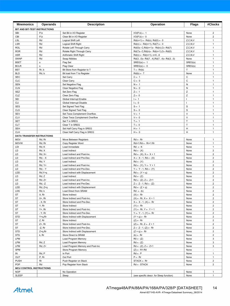
BIT AND BIT-TEST INSTRUCTIONS
SBI P,b Set Bit in I/O Register I/O(P,b) 1 None 2
CBI P,b Clear Bit in I/O Register I/O(P,b) 0 None 2
LSL Rd Logical Shift Left Rd(n+1) Rd(n), Rd(0) 0 Z,C,N,V 1
LSR Rd Logical Shift Right Rd(n) Rd(n+1), Rd(7) 0 Z,C,N,V 1
ROL Rd Rotate Left Through Carry Rd(0)C,Rd(n+1) Rd(n),CRd(7) Z,C,N,V 1
ROR Rd Rotate Right Through Carry Rd(7)C,Rd(n) Rd(n+1),CRd(0) Z,C,N,V 1
ASR Rd Arithmetic Shift Right Rd(n) Rd(n+1), n=0...6 Z,C,N,V 1
SWAP Rd Swap Nibbles Rd(3...0)Rd(7...4),Rd(7...4)Rd(3...0) None 1
BSET s Flag Set SREG(s) 1 SREG(s) 1
BCLR s Flag Clear SREG(s) 0 SREG(s) 1
BST Rr, b Bit Store from Register to T T Rr(b) T 1
BLD Rd, b Bit load from T to Register Rd(b) T None 1
SEC Set Carry C 1 C 1
CLC Clear Carry C 0 C 1
SEN Set Negative Flag N 1 N 1
CLN Clear Negative Flag N 0 N 1
SEZ Set Zero Flag Z 1 Z 1
CLZ Clear Zero Flag Z 0 Z 1
SEI Global Interrupt Enable I 1 I 1
CLI Global Interrupt Disable I 0 I 1
SES Set Signed Test Flag S 1 S 1
CLS Clear Signed Test Flag S 0 S 1
SEV Set Twos Complement Overflow. V 1 V 1
CLV Clear Twos Complement Overflow V 0 V 1
SET Set T in SREG T 1 T 1
CLT Clear T in SREG T 0 T 1
SEH Set Half Carry Flag in SREG H 1 H 1
CLH Clear Half Carry Flag in SREG H 0 H 1
DATA TRANSFER INSTRUCTIONS
MOV Rd, Rr Move Between Registers Rd Rr None 1
MOVW Rd, Rr Copy Register Word Rd+1:Rd Rr+1:Rr None 1
LDI Rd, K Load Immediate Rd K None 1
LD Rd, X Load Indirect Rd (X) None 2
LD Rd, X+ Load Indirect and Post-Inc. Rd (X), X X + 1 None 2
LD Rd, - X Load Indirect and Pre-Dec. X X - 1, Rd (X) None 2
LD Rd, Y Load Indirect Rd (Y) None 2
LD Rd, Y+ Load Indirect and Post-Inc. Rd (Y), Y Y + 1 None 2
LD Rd, - Y Load Indirect and Pre-Dec. Y Y - 1, Rd (Y) None 2
LDD Rd,Y+q Load Indirect with Displacement Rd (Y + q) None 2
LD Rd, Z Load Indirect Rd (Z) None 2
LD Rd, Z+ Load Indirect and Post-Inc. Rd (Z), Z Z+1 None 2
LD Rd, -Z Load Indirect and Pre-Dec. Z Z - 1, Rd (Z) None 2
LDD Rd, Z+q Load Indirect with Displacement Rd (Z + q) None 2
LDS Rd, k Load Direct from SRAM Rd (k) None 2
ST X, Rr Store Indirect (X) Rr None 2
ST X+, Rr Store Indirect and Post-Inc. (X) Rr, X X + 1 None 2
ST - X, Rr Store Indirect and Pre-Dec. X X - 1, (X) Rr None 2
ST Y, Rr Store Indirect (Y) Rr None 2
ST Y+, Rr Store Indirect and Post-Inc. (Y) Rr, Y Y + 1 None 2
ST - Y, Rr Store Indirect and Pre-Dec. Y Y - 1, (Y) Rr None 2
STD Y+q,Rr Store Indirect with Displacement (Y + q) Rr None 2
ST Z, Rr Store Indirect (Z) Rr None 2
ST Z+, Rr Store Indirect and Post-Inc. (Z) Rr, Z Z + 1 None 2
ST -Z, Rr Store Indirect and Pre-Dec. Z Z - 1, (Z) Rr None 2
STD Z+q,Rr Store Indirect with Displacement (Z + q) Rr None 2
STS k, Rr Store Direct to SRAM (k) Rr None 2
LPM Load Program Memory R0 (Z) None 3
LPM Rd, Z Load Program Memory Rd (Z) None 3
LPM Rd, Z+ Load Program Memory and Post-Inc Rd (Z), Z Z+1 None 3
SPM Store Program Memory (Z) R1:R0 None -
IN Rd, P In Port Rd P None 1
OUT P, Rr Out Port P Rr None 1
PUSH Rr Push Register on Stack STACK Rr None 2
POP Rd Pop Register from Stack Rd STACK None 2
MCU CONTROL INSTRUCTIONS
NOP No Operation None 1
SLEEP Sleep (see specific descr. for Sleep function) None 1
Mnemonics Operands Description Operation Flags #Clocks
14ATmega48A/PA/88A/PA/168A/PA/328/P [DATASHEET]Atmel-8271HS-AVR- ATmega-Datasheet Summary_08/2014

Note: 1. These instructions are only available in ATmega168PA and ATmega328P.
WDR Watchdog Reset (see specific descr. for WDR/timer) None 1
BREAK Break For On-chip Debug Only None N/A
Mnemonics Operands Description Operation Flags #Clocks
15ATmega48A/PA/88A/PA/168A/PA/328/P [DATASHEET]Atmel-8271HS-AVR- ATmega-Datasheet Summary_08/2014
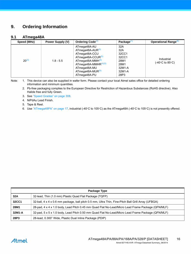
9. Ordering Information
9.1 ATmega48A
Note: 1. This device can also be supplied in wafer form. Please contact your local Atmel sales office for detailed ordering information and minimum quantities.
2. Pb-free packaging complies to the European Directive for Restriction of Hazardous Substances (RoHS directive). Also Halide free and fully Green.
3. See ”Speed Grades” on page 308.
4. NiPdAu Lead Finish.
5. Tape & Reel.
6. Use ”ATmega48PA” on page 17, industrial (-40C to 105C) as the ATmega48A (-40C to 105C) is not presently offered.
Speed (MHz) Power Supply (V) Ordering Code(2) Package(1) Operational Range(6)
20(3) 1.8 - 5.5
ATmega48A-AUATmega48A-AUR(5)
ATmega48A-CCUATmega48A-CCUR(5)
ATmega48A-MMH(4)
ATmega48A-MMHR(4)(5)
ATmega48A-MUATmega48A-MUR(5)
ATmega48A-PU
32A32A32CC132CC128M128M132M1-A32M1-A28P3
Industrial(-40C to 85C)
Package Type
32A 32-lead, Thin (1.0 mm) Plastic Quad Flat Package (TQFP)
32CC1 32-ball, 4 x 4 x 0.6 mm package, ball pitch 0.5 mm, Ultra Thin, Fine-Pitch Ball Grill Array (UFBGA)
28M1 28-pad, 4 x 4 x 1.0 body, Lead Pitch 0.45 mm Quad Flat No-Lead/Micro Lead Frame Package (QFN/MLF)
32M1-A 32-pad, 5 x 5 x 1.0 body, Lead Pitch 0.50 mm Quad Flat No-Lead/Micro Lead Frame Package (QFN/MLF)
28P3 28-lead, 0.300” Wide, Plastic Dual Inline Package (PDIP)
16ATmega48A/PA/88A/PA/168A/PA/328/P [DATASHEET]Atmel-8271HS-AVR- ATmega-Datasheet Summary_08/2014
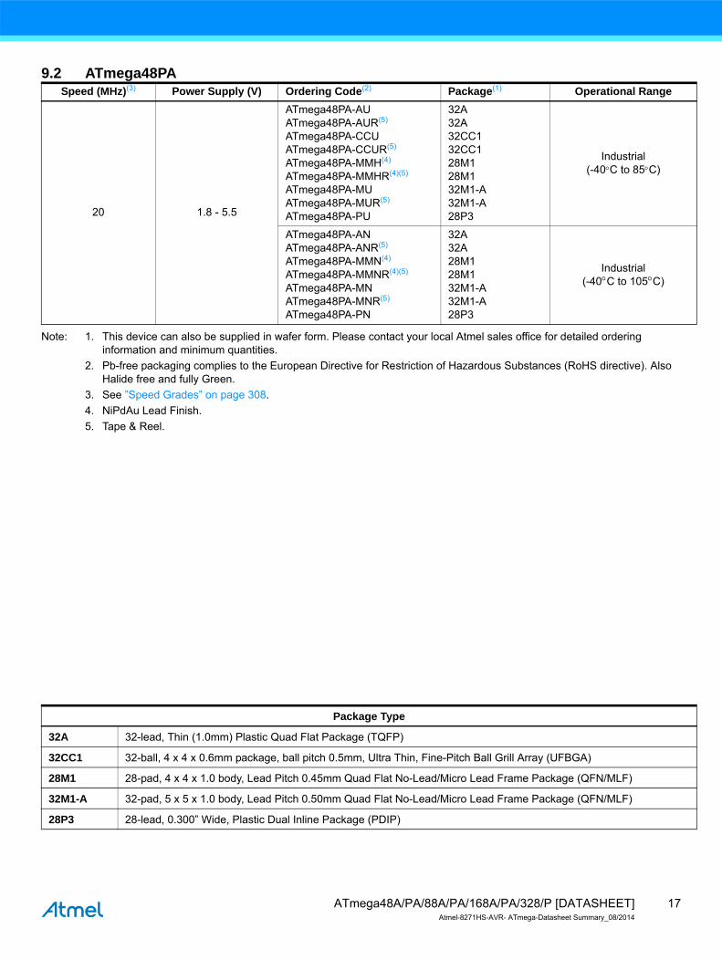
9.2 ATmega48PA
Note: 1. This device can also be supplied in wafer form. Please contact your local Atmel sales office for detailed ordering information and minimum quantities.
2. Pb-free packaging complies to the European Directive for Restriction of Hazardous Substances (RoHS directive). Also Halide free and fully Green.
3. See ”Speed Grades” on page 308.
4. NiPdAu Lead Finish.
5. Tape & Reel.
Speed (MHz)(3) Power Supply (V) Ordering Code(2) Package(1) Operational Range
20 1.8 - 5.5
ATmega48PA-AUATmega48PA-AUR(5)
ATmega48PA-CCUATmega48PA-CCUR(5)
ATmega48PA-MMH(4)
ATmega48PA-MMHR(4)(5)
ATmega48PA-MUATmega48PA-MUR(5)
ATmega48PA-PU
32A32A32CC132CC128M128M132M1-A32M1-A28P3
Industrial(-40C to 85C)
ATmega48PA-ANATmega48PA-ANR(5)
ATmega48PA-MMN(4)
ATmega48PA-MMNR(4)(5)
ATmega48PA-MNATmega48PA-MNR(5)
ATmega48PA-PN
32A32A28M128M132M1-A32M1-A28P3
Industrial(-40C to 105C)
Package Type
32A 32-lead, Thin (1.0mm) Plastic Quad Flat Package (TQFP)
32CC1 32-ball, 4 x 4 x 0.6mm package, ball pitch 0.5mm, Ultra Thin, Fine-Pitch Ball Grill Array (UFBGA)
28M1 28-pad, 4 x 4 x 1.0 body, Lead Pitch 0.45mm Quad Flat No-Lead/Micro Lead Frame Package (QFN/MLF)
32M1-A 32-pad, 5 x 5 x 1.0 body, Lead Pitch 0.50mm Quad Flat No-Lead/Micro Lead Frame Package (QFN/MLF)
28P3 28-lead, 0.300” Wide, Plastic Dual Inline Package (PDIP)
17ATmega48A/PA/88A/PA/168A/PA/328/P [DATASHEET]Atmel-8271HS-AVR- ATmega-Datasheet Summary_08/2014
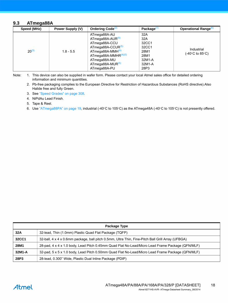
9.3 ATmega88A
Note: 1. This device can also be supplied in wafer form. Please contact your local Atmel sales office for detailed ordering information and minimum quantities.
2. Pb-free packaging complies to the European Directive for Restriction of Hazardous Substances (RoHS directive).Also Halide free and fully Green.
3. See ”Speed Grades” on page 308.
4. NiPdAu Lead Finish.
5. Tape & Reel.
6. Use ”ATmega88PA” on page 19, industrial (-40C to 105C) as the ATmega48A (-40C to 105C) is not presently offered.
Speed (MHz) Power Supply (V) Ordering Code(2) Package(1) Operational Range(6)
20(3) 1.8 - 5.5
ATmega88A-AUATmega88A-AUR(5)
ATmega88A-CCUATmega88A-CCUR(5)
ATmega88A-MMH(4)
ATmega88A-MMHR(4)(5)
ATmega88A-MUATmega88A-MUR(5)
ATmega88A-PU
32A32A32CC132CC128M128M132M1-A32M1-A28P3
Industrial(-40C to 85C)
Package Type
32A 32-lead, Thin (1.0mm) Plastic Quad Flat Package (TQFP)
32CC1 32-ball, 4 x 4 x 0.6mm package, ball pitch 0.5mm, Ultra Thin, Fine-Pitch Ball Grill Array (UFBGA)
28M1 28-pad, 4 x 4 x 1.0 body, Lead Pitch 0.45mm Quad Flat No-Lead/Micro Lead Frame Package (QFN/MLF)
32M1-A 32-pad, 5 x 5 x 1.0 body, Lead Pitch 0.50mm Quad Flat No-Lead/Micro Lead Frame Package (QFN/MLF)
28P3 28-lead, 0.300” Wide, Plastic Dual Inline Package (PDIP)
18ATmega48A/PA/88A/PA/168A/PA/328/P [DATASHEET]Atmel-8271HS-AVR- ATmega-Datasheet Summary_08/2014

9.4 ATmega88PA
Note: 1. This device can also be supplied in wafer form. Please contact your local Atmel sales office for detailed ordering information and minimum quantities.
2. Pb-free packaging complies to the European Directive for Restriction of Hazardous Substances (RoHS directive).Also Halide free and fully Green.
3. See ”Speed Grades” on page 308.
4. NiPdAu Lead Finish.
5. Tape & Reel.
Speed (MHz)(3) Power Supply (V) Ordering Code(2) Package(1) Operational Range
20 1.8 - 5.5
ATmega88PA-AUATmega88PA-AUR(5)
ATmega88PA-CCUATmega88PA-CCUR(5)
ATmega88PA-MMH(4)
ATmega88PA-MMHR(4)(5)
ATmega88PA-MUATmega88PA-MUR(5)
ATmega88PA-PU
32A32A32CC132CC128M128M132M1-A32M1-A28P3
Industrial(-40C to 85C)
ATmega88PA-ANATmega88PA-ANR(5)
ATmega88PA-MMN(4)
ATmega88PA-MMNR(4)(5)
ATmega88PA-MNATmega88PA-MNR(5)
ATmega88PA-PN
32A32A28M128M132M1-A32M1-A28P3
Industrial(-40C to 105C)
Package Type
32A 32-lead, Thin (1.0mm) Plastic Quad Flat Package (TQFP)
32CC1 32-ball, 4 x 4 x 0.6mm package, ball pitch 0.5 mm, Ultra Thin, Fine-Pitch Ball Grill Array (UFBGA)
28M1 28-pad, 4 x 4 x 1.0 body, Lead Pitch 0.45 mm Quad Flat No-Lead/Micro Lead Frame Package (QFN/MLF)
32M1-A 32-pad, 5 x 5 x 1.0 body, Lead Pitch 0.50 mm Quad Flat No-Lead/Micro Lead Frame Package (QFN/MLF)
28P3 28-lead, 0.300” Wide, Plastic Dual Inline Package (PDIP)
19ATmega48A/PA/88A/PA/168A/PA/328/P [DATASHEET]Atmel-8271HS-AVR- ATmega-Datasheet Summary_08/2014
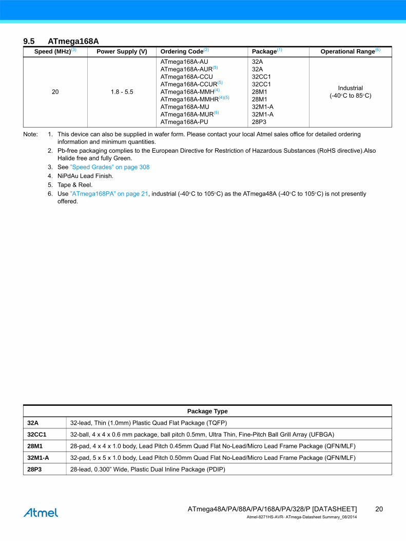
9.5 ATmega168A
Note: 1. This device can also be supplied in wafer form. Please contact your local Atmel sales office for detailed ordering information and minimum quantities.
2. Pb-free packaging complies to the European Directive for Restriction of Hazardous Substances (RoHS directive).Also Halide free and fully Green.
3. See ”Speed Grades” on page 308
4. NiPdAu Lead Finish.
5. Tape & Reel.
6. Use ”ATmega168PA” on page 21, industrial (-40C to 105C) as the ATmega48A (-40C to 105C) is not presently offered.
Speed (MHz)(3) Power Supply (V) Ordering Code(2) Package(1) Operational Range(6)
20 1.8 - 5.5
ATmega168A-AUATmega168A-AUR(5)
ATmega168A-CCUATmega168A-CCUR(5)
ATmega168A-MMH(4)
ATmega168A-MMHR(4)(5)
ATmega168A-MUATmega168A-MUR(5)
ATmega168A-PU
32A32A32CC132CC128M128M132M1-A32M1-A28P3
Industrial(-40C to 85C)
Package Type
32A 32-lead, Thin (1.0mm) Plastic Quad Flat Package (TQFP)
32CC1 32-ball, 4 x 4 x 0.6 mm package, ball pitch 0.5mm, Ultra Thin, Fine-Pitch Ball Grill Array (UFBGA)
28M1 28-pad, 4 x 4 x 1.0 body, Lead Pitch 0.45mm Quad Flat No-Lead/Micro Lead Frame Package (QFN/MLF)
32M1-A 32-pad, 5 x 5 x 1.0 body, Lead Pitch 0.50mm Quad Flat No-Lead/Micro Lead Frame Package (QFN/MLF)
28P3 28-lead, 0.300” Wide, Plastic Dual Inline Package (PDIP)
20ATmega48A/PA/88A/PA/168A/PA/328/P [DATASHEET]Atmel-8271HS-AVR- ATmega-Datasheet Summary_08/2014
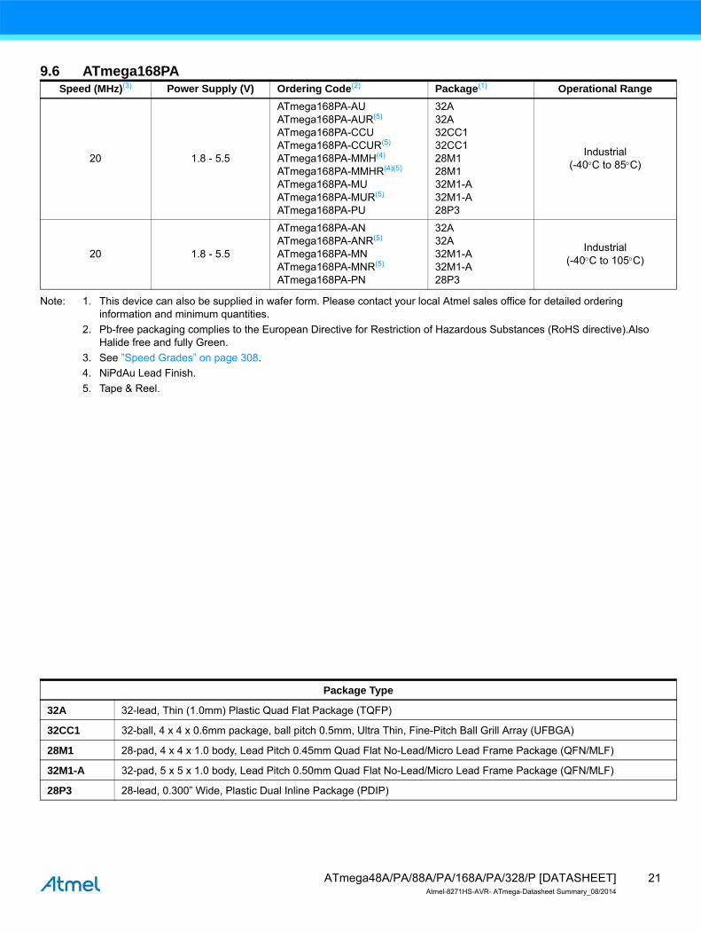
9.6 ATmega168PA
Note: 1. This device can also be supplied in wafer form. Please contact your local Atmel sales office for detailed ordering information and minimum quantities.
2. Pb-free packaging complies to the European Directive for Restriction of Hazardous Substances (RoHS directive).Also Halide free and fully Green.
3. See ”Speed Grades” on page 308.
4. NiPdAu Lead Finish.
5. Tape & Reel.
Speed (MHz)(3) Power Supply (V) Ordering Code(2) Package(1) Operational Range
20 1.8 - 5.5
ATmega168PA-AUATmega168PA-AUR(5)
ATmega168PA-CCUATmega168PA-CCUR(5)
ATmega168PA-MMH(4)
ATmega168PA-MMHR(4)(5)
ATmega168PA-MUATmega168PA-MUR(5)
ATmega168PA-PU
32A32A32CC132CC128M128M132M1-A32M1-A28P3
Industrial(-40C to 85C)
20 1.8 - 5.5
ATmega168PA-ANATmega168PA-ANR(5)
ATmega168PA-MNATmega168PA-MNR(5)
ATmega168PA-PN
32A32A32M1-A32M1-A28P3
Industrial(-40C to 105C)
Package Type
32A 32-lead, Thin (1.0mm) Plastic Quad Flat Package (TQFP)
32CC1 32-ball, 4 x 4 x 0.6mm package, ball pitch 0.5mm, Ultra Thin, Fine-Pitch Ball Grill Array (UFBGA)
28M1 28-pad, 4 x 4 x 1.0 body, Lead Pitch 0.45mm Quad Flat No-Lead/Micro Lead Frame Package (QFN/MLF)
32M1-A 32-pad, 5 x 5 x 1.0 body, Lead Pitch 0.50mm Quad Flat No-Lead/Micro Lead Frame Package (QFN/MLF)
28P3 28-lead, 0.300” Wide, Plastic Dual Inline Package (PDIP)
21ATmega48A/PA/88A/PA/168A/PA/328/P [DATASHEET]Atmel-8271HS-AVR- ATmega-Datasheet Summary_08/2014
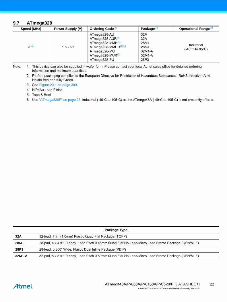
9.7 ATmega328
Note: 1. This device can also be supplied in wafer form. Please contact your local Atmel sales office for detailed ordering information and minimum quantities.
2. Pb-free packaging complies to the European Directive for Restriction of Hazardous Substances (RoHS directive).Also Halide free and fully Green.
3. See Figure 29-1 on page 309.
4. NiPdAu Lead Finish.
5. Tape & Reel
6. Use ”ATmega328P” on page 23, industrial (-40C to 105C) as the ATmega48A (-40C to 105C) is not presently offered.
Speed (MHz) Power Supply (V) Ordering Code(2) Package(1) Operational Range(6)
20(3) 1.8 - 5.5
ATmega328-AUATmega328-AUR(5)
ATmega328-MMH(4)
ATmega328-MMHR(4)(5)
ATmega328-MUATmega328-MUR(5)
ATmega328-PU
32A32A28M128M132M1-A32M1-A28P3
Industrial(-40C to 85C)
Package Type
32A 32-lead, Thin (1.0mm) Plastic Quad Flat Package (TQFP)
28M1 28-pad, 4 x 4 x 1.0 body, Lead Pitch 0.45mm Quad Flat No-Lead/Micro Lead Frame Package (QFN/MLF)
28P3 28-lead, 0.300” Wide, Plastic Dual Inline Package (PDIP)
32M1-A 32-pad, 5 x 5 x 1.0 body, Lead Pitch 0.50mm Quad Flat No-Lead/Micro Lead Frame Package (QFN/MLF)
22ATmega48A/PA/88A/PA/168A/PA/328/P [DATASHEET]Atmel-8271HS-AVR- ATmega-Datasheet Summary_08/2014
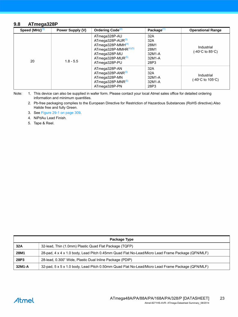
9.8 ATmega328P
Note: 1. This device can also be supplied in wafer form. Please contact your local Atmel sales office for detailed ordering information and minimum quantities.
2. Pb-free packaging complies to the European Directive for Restriction of Hazardous Substances (RoHS directive).Also Halide free and fully Green.
3. See Figure 29-1 on page 309.
4. NiPdAu Lead Finish.
5. Tape & Reel.
Speed (MHz)(3) Power Supply (V) Ordering Code(2) Package(1) Operational Range
20 1.8 - 5.5
ATmega328P-AUATmega328P-AUR(5)
ATmega328P-MMH(4)
ATmega328P-MMHR(4)(5)
ATmega328P-MUATmega328P-MUR(5)
ATmega328P-PU
32A32A28M128M132M1-A32M1-A28P3
Industrial(-40C to 85C)
ATmega328P-ANATmega328P-ANR(5)
ATmega328P-MNATmega328P-MNR(5)
ATmega328P-PN
32A32A32M1-A32M1-A28P3
Industrial(-40C to 105C)
Package Type
32A 32-lead, Thin (1.0mm) Plastic Quad Flat Package (TQFP)
28M1 28-pad, 4 x 4 x 1.0 body, Lead Pitch 0.45mm Quad Flat No-Lead/Micro Lead Frame Package (QFN/MLF)
28P3 28-lead, 0.300” Wide, Plastic Dual Inline Package (PDIP)
32M1-A 32-pad, 5 x 5 x 1.0 body, Lead Pitch 0.50mm Quad Flat No-Lead/Micro Lead Frame Package (QFN/MLF)
23ATmega48A/PA/88A/PA/168A/PA/328/P [DATASHEET]Atmel-8271HS-AVR- ATmega-Datasheet Summary_08/2014
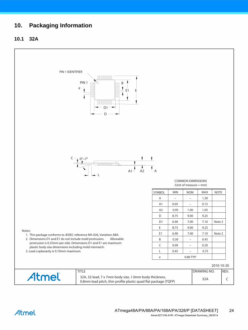
10. Packaging Information
10.1 32A
TITLE DRAWING NO. REV.
32A, 32-lead, 7 x 7mm body size, 1.0mm body thickness,0.8mm lead pitch, thin profile plastic quad flat package (TQFP)
C32A
2010-10-20
PIN 1 IDENTIFIER
0°~7°
PIN 1
L
C
A1 A2 A
D1
D
eE1 E
B
Notes: 1. This package conforms to JEDEC reference MS-026, Variation ABA. 2. Dimensions D1 and E1 do not include mold protrusion. Allowable protrusion is 0.25mm per side. Dimensions D1 and E1 are maximum plastic body size dimensions including mold mismatch. 3. Lead coplanarity is 0.10mm maximum.
A – – 1.20
A1 0.05 – 0.15
A2 0.95 1.00 1.05
D 8.75 9.00 9.25
D1 6.90 7.00 7.10 Note 2
E 8.75 9.00 9.25
E1 6.90 7.00 7.10 Note 2
B 0.30 – 0.45
C 0.09 – 0.20
L 0.45 – 0.75
e 0.80 TYP
COMMON DIMENSIONS(Unit of measure = mm)
SYMBOL MIN NOM MAX NOTE
24ATmega48A/PA/88A/PA/168A/PA/328/P [DATASHEET]Atmel-8271HS-AVR- ATmega-Datasheet Summary_08/2014
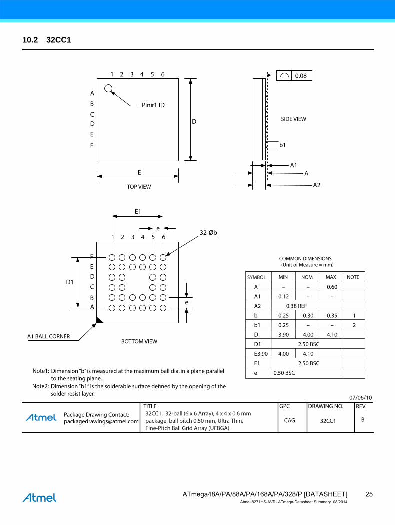
10.2 32CC1
TITLE DRAWING NO.GPC REV. Package Drawing Contact: [email protected] BCAG
32CC1, 32-ball (6 x 6 Array), 4 x 4 x 0.6 mm package, ball pitch 0.50 mm, Ultra Thin, Fine-Pitch Ball Grid Array (UFBGA)
32CC1
A – – 0.60
A1 0.12 – –
A2 0.38 REF
b 0.25 0.30 0.35 1
b1 0.25 – – 2
D 3.90 4.00 4.10
D1 2.50 BSC
E 3.90 4.00 4.10
E1 2.50 BSC
e 0.50 BSC
07/06/10
b1
COMMON DIMENSIONS(Unit of Measure = mm)
1 2 3 4 5 6
BA
C
D
E
F
E
D
e
32-Øb
E
D
B
A
Pin#1 ID
0.08
A1A
D1
E1
A2
A1 BALL CORNER
1 2 3 4 5 6
F
CSIDE VIEW
BOTTOM VIEW
TOP VIEW
SYMBOL MIN NOM MAX NOTE
Note1: Dimension “b” is measured at the maximum ball dia. in a plane parallel to the seating plane. Note2: Dimension “b1” is the solderable surface defined by the opening of the solder resist layer.
e
25ATmega48A/PA/88A/PA/168A/PA/328/P [DATASHEET]Atmel-8271HS-AVR- ATmega-Datasheet Summary_08/2014
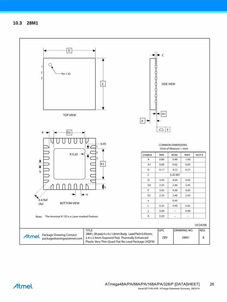
10.3 28M1
TITLE DRAWING NO.GPC REV. Package Drawing Contact: [email protected] 28M1ZBV B
28M1, 28-pad, 4 x 4 x 1.0mm Body, Lead Pitch 0.45mm, 2.4 x 2.4mm Exposed Pad, Thermally Enhanced Plastic Very Thin Quad Flat No Lead Package (VQFN)
10/24/08
SIDE VIEW
Pin 1 ID
BOTTOM VIEW
TOP VIEW
Note: The terminal #1 ID is a Laser-marked Feature.
D
E
e
K
A1
C
A
D2
E2
y
L
1
2
3
b
1
2
3
0.45 COMMON DIMENSIONS(Unit of Measure = mm)
SYMBOL MIN NOM MAX NOT E
A 0.80 0.90 1.00
A1 0.00 0.02 0.05
b 0.17 0.22 0.27
C 0.20 REF
D 3.95 4.00 4.05
D2 2.35 2.40 2.45
E 3.95 4.00 4.05
E2 2.35 2.40 2.45
e 0.45
L 0.35 0.40 0.45
y 0.00 – 0.08
K 0.20 – –
R 0.20
0.4 Ref(4x)
26ATmega48A/PA/88A/PA/168A/PA/328/P [DATASHEET]Atmel-8271HS-AVR- ATmega-Datasheet Summary_08/2014
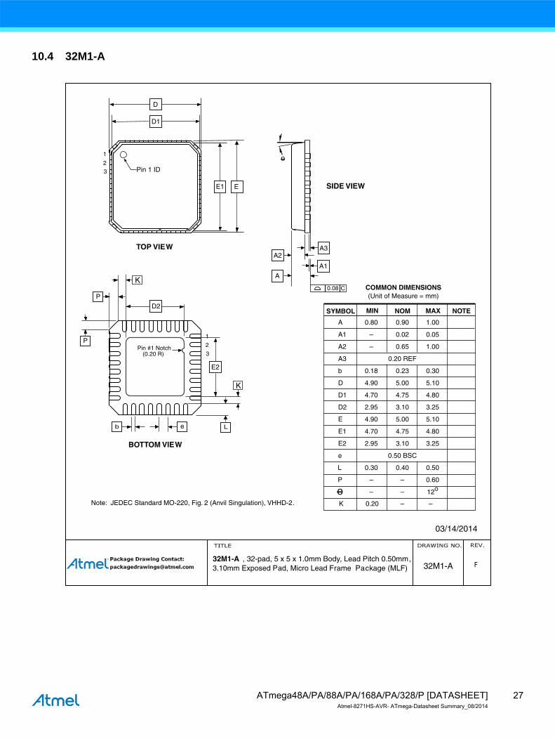
10.4 32M1-A
COMMON DIMENSIONS(Unit of Measure = mm)
SYMBOL MIN NOM MAX NOTE
D1
D
E1 E
eb
A3A2
A1 A
D2
E2
0.08 C
L
1
2
3
P
P
01
2
3
A 0.80 0.90 1.00
A1 – 0.02 0.05
A2 – 0.65 1.00
A3 0.20 REF
b 0.18 0.23 0.30
D
D1
D2 2.95 3.10 3.25
4.90 5.00 5.10
4.70 4.75 4.80
4.70 4.75 4.80
4.90 5.00 5.10
E
E1
E2 2.95 3.10 3.25
e 0.50 BSC
L 0.30 0.40 0.50
P – – 0.60
– – 12o
Note: JEDEC Standard MO-220, Fig. 2 (Anvil Singulation), VHHD-2.
TOP VIEW
SIDE VIEW
BOTTOM VIEW
0
Pin 1 ID
Pin #1 Notch(0.20 R)
K 0.20 – –
K
K
32M1-A , 32-pad, 5 x 5 x 1.0mm Body, Lead Pitch 0.50mm, 3.10mm Exposed Pad, Micro Lead Frame Package (MLF) 32M1-A
03/14/2014
F
27ATmega48A/PA/88A/PA/168A/PA/328/P [DATASHEET]Atmel-8271HS-AVR- ATmega-Datasheet Summary_08/2014
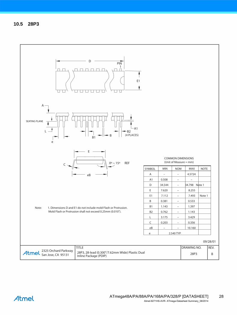
10.5 28P3
2325 Orchard Parkway San Jose, CA 95131
TITLE DRAWING NO. REV. 28P3, 28-lead (0.300"/7.62mm Wide) Plastic Dual Inline Package (PDIP) B28P3
09/28/01
PIN1
E1
A1
B
REF
E
B1
C
L
SEATING PLANE
A
0º ~ 15º
D
e
eB
B2(4 PLACES)
COMMON DIMENSIONS(Unit of Measure = mm)
SYMBOL MIN NOM MAX NOTE
A – – 4.5724
A1 0.508 – –
D 34.544 – 34.798 Note 1
E 7.620 – 8.255
E1 7.112 – 7.493 Note 1
B 0.381 – 0.533
B1 1.143 – 1.397
B2 0.762 – 1.143
L 3.175 – 3.429
C 0.203 – 0.356
eB – – 10.160
e 2.540 TYP
Note: 1. Dimensions D and E1 do not include mold Flash or Protrusion. Mold Flash or Protrusion shall not exceed 0.25mm (0.010").
28ATmega48A/PA/88A/PA/168A/PA/328/P [DATASHEET]Atmel-8271HS-AVR- ATmega-Datasheet Summary_08/2014
11. Errata
11.1 Errata ATmega48A
The revision letter in this section refers to the revision of the ATmega48A device.
11.1.1 Rev. D
• Analog MUX can be turned off when setting ACME bit
• TWI Data setup time can be too short
1. Analog MUX can be turned off when setting ACME bit
If the ACME (Analog Comparator Multiplexer Enabled) bit in ADCSRB is set while MUX3 in ADMUX is '1' (ADMUX[3:0]=1xxx), all MUXes are turned off until the ACME bit is cleared.
Problem Fix/Workaround
Clear the MUX3 bit before setting the ACME bit.
2. TWI Data setup time can be too short
When running the device as a TWI slave with a system clock above 2MHz, the data setup time for the first bit after ACK may in some cases be too short. This may cause a false start or stop condition on the TWI line.
Problem Fix/Workaround
Insert a delay between setting TWDR and TWCR.
11.2 Errata ATmega48PA
The revision letter in this section refers to the revision of the ATmega48PA device.
11.2.1 Rev. A
• Power consumption in power save modes
• Startup time for the device
1. Power consumption in power save modes
Power consumption in power save modes will be higher due to improper control of internal power
management.48
Problem Fix/Workaround
This problem will be corrected in Rev B.
2. Startup time for the device
Due to implementation of a different NVM structure, the startup sequence for the device will require
longer startup time.
Problem Fix/Workaround
There is no fix for this problem.
11.2.2 Rev. D
• Analog MUX can be turned off when setting ACME bit
• TWI Data setup time can be too short
1. Analog MUX can be turned off when setting ACME bit
29ATmega48A/PA/88A/PA/168A/PA/328/P [DATASHEET]Atmel-8271HS-AVR- ATmega-Datasheet Summary_08/2014
If the ACME (Analog Comparator Multiplexer Enabled) bit in ADCSRB is set while MUX3 in ADMUX is '1' (ADMUX[3:0]=1xxx), all MU Xes are turned off until the ACME bit is cleared.
Problem Fix/Workaround
Clear the MUX3 bit before setting the ACME bit.
2. TWI Data setup time can be too short
When running the device as a TWI slave with a system clock above 2MHz, the data setup time for the first bit after ACK may in some cases be too short. This may cause a false start or stop condition on the TWI line.
Problem Fix/Workaround
Insert a delay between setting TWDR and TWCR.
11.3 Errata ATmega88A
The revision letter in this section refers to the revision of the ATmega88A device.
11.3.1 Rev. F
• Analog MUX can be turned off when setting ACME bit
• TWI Data setup time can be too short
1. Analog MUX can be turned off when setting ACME bit
If the ACME (Analog Comparator Multiplexer Enabled) bit in ADCSRB is set while MUX3 in ADMUX is '1' (ADMUX[3:0]=1xxx), all MU Xes are turned off until the ACME bit is cleared.
Problem Fix/Workaround
Clear the MUX3 bit before setting the ACME bit.
2. TWI Data setup time can be too short
When running the device as a TWI slave with a system clock above 2MHz, the data setup time for the first bit after ACK may in some cases be too short. This may cause a false start or stop condition on the TWI line.
Problem Fix/Workaround
Insert a delay between setting TWDR and TWCR.
11.4 Errata ATmega88PA
The revision letter in this section refers to the revision of the ATmega88PA device.
11.4.1 Rev. F
• Analog MUX can be turned off when setting ACME bit
• TWI Data setup time can be too short
1. Analog MUX can be turned off when setting ACME bit
If the ACME (Analog Comparator Multiplexer Enabled) bit in ADCSRB is set while MUX3 in ADMUX is '1' (ADMUX[3:0]=1xxx), all MUXes are turned off until the ACME bit is cleared.
Problem Fix/Workaround
Clear the MUX3 bit before setting the ACME bit.
2. TWI Data setup time can be too short
30ATmega48A/PA/88A/PA/168A/PA/328/P [DATASHEET]Atmel-8271HS-AVR- ATmega-Datasheet Summary_08/2014
When running the device as a TWI slave with a system clock above 2MHz, the data setup time for the first bit after ACK may in some cases be too short. This may cause a false start or stop condition on the TWI line.
Problem Fix/Workaround
Insert a delay between setting TWDR and TWCR.
11.4.2 Rev. A
• Power consumption in power save modes
• Startup time for the device
1. Power consumption in power save modes
Power consumption in power save modes will be higher due to improper control of internal power
management.48
Problem Fix/Workaround
This problem will be corrected in Rev B.
2. Startup time for the device
Due to implementation of a different NVM structure, the startup sequence for the device will require
longer startup time.
Problem Fix/Workaround
There is no fix for this problem.
11.5 Errata ATmega168A
The revision letter in this section refers to the revision of the ATmega168A device.
11.5.1 Rev. E
• Analog MUX can be turned off when setting ACME bit
• TWI Data setup time can be too short
1. Analog MUX can be turned off when setting ACME bit
If the ACME (Analog Comparator Multiplexer Enabled) bit in ADCSRB is set while MUX3 in ADMUX is '1' (ADMUX[3:0]=1xxx), all MUXes are turned off until the ACME bit is cleared.
Problem Fix/Workaround
Clear the MUX3 bit before setting the ACME bit.
2. TWI Data setup time can be too short
When running the device as a TWI slave with a system clock above 2MHz, the data setup time for the first bit after ACK may in some cases be too short. This may cause a false start or stop condition on the TWI line.
Problem Fix/Workaround
Insert a delay between setting TWDR and TWCR.
11.6 Errata ATmega168PA
The revision letter in this section refers to the revision of the ATmega168PA device.
31ATmega48A/PA/88A/PA/168A/PA/328/P [DATASHEET]Atmel-8271HS-AVR- ATmega-Datasheet Summary_08/2014
11.6.1 Rev E
• Analog MUX can be turned off when setting ACME bit
• TWI Data setup time can be too short
1. Analog MUX can be turned off when setting ACME bit
If the ACME (Analog Comparator Multiplexer Enabled) bit in ADCSRB is set while MUX3 in ADMUX is '1' (ADMUX[3:0]=1xxx), all MUXes are turned off until the ACME bit is cleared.
Problem Fix/Workaround
Clear the MUX3 bit before setting the ACME bit.
2. TWI Data setup time can be too short
When running the device as a TWI slave with a system clock above 2MHz, the data setup time for the first bit after ACK may in some cases be too short. This may cause a false start or stop condition on the TWI line.
Problem Fix/Workaround
Insert a delay between setting TWDR and TWCR.
32ATmega48A/PA/88A/PA/168A/PA/328/P [DATASHEET]Atmel-8271HS-AVR- ATmega-Datasheet Summary_08/2014
11.7 Errata ATmega328
The revision letter in this section refers to the revision of the ATmega328 device.
11.7.1 Rev D
• Analog MUX can be turned off when setting ACME bit
• TWI Data setup time can be too short
1. Analog MUX can be turned off when setting ACME bit
If the ACME (Analog Comparator Multiplexer Enabled) bit in ADCSRB is set while MUX3 in ADMUX is '1' (ADMUX[3:0]=1xxx), all MUX es are turned off until the ACME bit is cleared.
Problem Fix/Workaround
Clear the MUX3 bit before setting the ACME bit.
2. TWI Data setup time can be too short
When running the device as a TWI slave with a system clock above 2MHz, the data setup time for the first bit after ACK may in some cases be too short. This may cause a false start or stop condition on the TWI line.
Problem Fix/Workaround
Insert a delay between setting TWDR and TWCR.
11.7.2 Rev C
Not sampled.
11.7.3 Rev B
• Analog MUX can be turned off when setting ACME bit
• Unstable 32kHz Oscillator
1. Analog MUX can be turned off when setting ACME bit
If the ACME (Analog Comparator Multiplexer Enabled) bit in ADCSRB is set while MUX3 in ADMUX is '1' (ADMUX[3:0]=1xxx), all MUXes are turned off until the ACME bit is cleared.
Problem Fix/Workaround
Clear the MUX3 bit before setting the ACME bit.
2. Unstable 32kHz Oscillator
The 32kHz oscillator does not work as system clock. The 32kHz oscillator used as asynchronous timer is inaccurate.
Problem Fix/ Workaround
None.
11.7.4 Rev A
• Analog MUX can be turned off when setting ACME bit
• Unstable 32kHz Oscillator
1. Analog MUX can be turned off when setting ACME bit
If the ACME (Analog Comparator Multiplexer Enabled) bit in ADCSRB is set while MUX3 in ADMUX is '1' (ADMUX[3:0]=1xxx), all MUXes are turned off until the ACME bit is cleared.
33ATmega48A/PA/88A/PA/168A/PA/328/P [DATASHEET]Atmel-8271HS-AVR- ATmega-Datasheet Summary_08/2014
Problem Fix/Workaround
Clear the MUX3 bit before setting the ACME bit.
2. Unstable 32kHz Oscillator
The 32kHz oscillator does not work as system clock. The 32kHz oscillator used as asynchronous timer is inaccurate.
Problem Fix/ Workaround
None.
11.8 Errata ATmega328P
The revision letter in this section refers to the revision of the ATmega328P device.
11.8.1 Rev D
• Analog MUX can be turned off when setting ACME bit
• TWI Data setup time can be too short
1. Analog MUX can be turned off when setting ACME bit
If the ACME (Analog Comparator Multiplexer Enabled) bit in ADCSRB is set while MUX3 in ADMUX is '1' (ADMUX[3:0]=1xxx), all MUXes are turned off until the ACME bit is cleared.
Problem Fix/Workaround
Clear the MUX3 bit before setting the ACME bit.
2. TWI Data setup time can be too short
When running the device as a TWI slave with a system clock above 2MHz, the data setup time for the first bit after ACK may in some cases be too short. This may cause a false start or stop condition on the TWI line.
Problem Fix/Workaround
Insert a delay between setting TWDR and TWCR.
11.8.2 Rev C
Not sampled.
11.8.3 Rev B
• Analog MUX can be turned off when setting ACME bit
• Unstable 32kHz Oscillator
1. Analog MUX can be turned off when setting ACME bit
If the ACME (Analog Comparator Multiplexer Enabled) bit in ADCSRB is set while MUX3 in ADMUX is '1' (ADMUX[3:0]=1xxx), all MUXes are turned off until the ACME bit is cleared.
Problem Fix/Workaround
Clear the MUX3 bit before setting the ACME bit.
2. Unstable 32kHz Oscillator
The 32kHz oscillator does not work as system clock. The 32kHz oscillator used as asynchronous timer is inaccurate.
Problem Fix/ Workaround
34ATmega48A/PA/88A/PA/168A/PA/328/P [DATASHEET]Atmel-8271HS-AVR- ATmega-Datasheet Summary_08/2014
None.
11.8.4 Rev A
• Unstable 32kHz Oscillator
1. Unstable 32kHz Oscillator
The 32kHz oscillator does not work as system clock. The 32kHz oscillator used as asynchronous timer is inaccurate.
Problem Fix/ Workaround
None.
35ATmega48A/PA/88A/PA/168A/PA/328/P [DATASHEET]Atmel-8271HS-AVR- ATmega-Datasheet Summary_08/2014
12. Datasheet Revision History
Please note that the referring page numbers in this section are referred to this document. The referring revision in this section are referring to the document revision.
12.1 Rev. 8271H – 08/2013
12.2 Rev. 8271G – 02/2013
12.3 Rev. 8271F – 08/2012
1.Updated text in section Section 16.9.3 ”Fast PWM Mode” on page 124 concerning compare units allowing generation of PWM waveforms (on page 126), referring to table 16-2.
2. Updated WDT Assembly code example in Section 10.10.5 ”Watchdog Timer” on page 44 (and onwards)
3.
Updated footnote 1 for tables giving DC Characteristics in ”ATmega48PA DC Characteristics – Current Consumption” on page 320, ”ATmega88PA DC Characteristics – Current Consumption” on page 321, ”ATmega168P DC Characteristics – Current Consumption” on page 321 and ”ATmega328P DC Characteristics – Current Consumption” on page 322.
4. Figure 31-1 on page 324 has been updated with the correct plot.
5. Figure 31-333 on page 499 has been updated with the correct plot.
6. Changed description of external interrupt behavior in deep sleep in Section 13. ”External Interrupts” on page 71.
7. Added wait delay for tWD_FUSE in Table 28-18 on page 298.
7. Updated errata for rev A of 48PA and 88PA in Section 11.2 on page 29 and Section 11.4 on page 30.
8. Updated back page and footer according to datasheet template of 05/2014
1. Added ”Electrical Characteristics (TA = -40°C to 105°C)” on page 319.
2. Added ”ATmega48PA Typical Characteristics – (TA = -40°C to 105°C)” on page 523.
3. Added ”ATmega88PA Typical Characteristics – (TA = -40°C to 105°C)” on page 547.
4. Added ”ATmega168PA Typical Characteristics – (TA = -40°C to 105°C)” on page 571.
5. Added ”ATmega328P Typical Characteristics – (TA = -40°C to 105°C)” on page 596.
1. Added ”DC Characteristics” on page 301. The following tables for DC characteristics - TA = -40C to 105C added:
Table 29-4 on page 304
Table 29-7 on page 305
Table 29-10 on page 307
Table 29-13 on page 308
2. Replaced the following typical characteristics by the plots that include les characteristics at “TA = -40C to 105C”:
”ATmega48PA Typical Characteristics” on page 349
”ATmega88PA Typical Characteristics” on page 398
”ATmega168PA Typical Characteristics” on page 448
”ATmega328P Typical Characteristics” on page 498
36ATmega48A/PA/88A/PA/168A/PA/328/P [DATASHEET]Atmel-8271HS-AVR- ATmega-Datasheet Summary_08/2014
12.4 Rev. 8271E – 07/2012
12.5 Rev. 8271D – 05/11
12.6 Rev. 8271C – 08/10
3.Removed the Power Save (Psave) maximum numbers for all devices throughout ”Electrical Characteristics – (TA = -40°C to 85°C)” on page 301.
4.Changed the powerdown maximum numbers from 8.5 and 3µA to 10 and 5µA (ATmega48PA, ATmega88PA, ATmega168PA and ATmega328P).
5.Changed the table note “Maximum values are characterized values and not test limits in production” to “Max values are test limits in production throughout ”Electrical Characteristics – (TA = -40°C to 85°C)” on page 301.
1. Updated Figure 1-1 on page 3. Overlined “RESET” in 28 MLF top view and in 32 MLF top view.
2.Added EEAR9 bit to the ”EEARH and EEARL – The EEPROM Address Register” on page 22 and updated the all bit descriptions accordingly.
3.Added a footnote “EEAR9 and EEAR8 are unused bits in ATmega48A/48PA and must always be written to zero” to ”EEARH and EEARL – The EEPROM Address Register” on page 22.
4.Updated Table 18-8 on page 156, “Waveform Generation Mode Bit Description” . WGM2, WGM1 and WGM0 changed to WGM22, WGM21 and WGM20 respectively.
5.Updated ”TCCR2B – Timer/Counter Control Register B” on page 157. bit 2 (CS22) and bit 3 (WGM22) changed from R (read only) to R/W (read/write).
6. Updated the definition of fosc on page 173. fosc is the system clock frequency (not XTAL pin frequency)
7.Updated ”SPMCSR – Store Program Memory Control and Status Register” on page 263. Bit 0 renamed SPMEN and added bit 5 “SIGRD”.
8.Replaced “SELFPRGEN” by “SPMEN” throughout the whole datasheet including in the “code examples”, except in ”Program And Data Memory Lock Bits” on page 282 and in ”Fuse Bits” on page 283.
9. Updated ”Register Summary” on page 9 to include the bits: SIGRD and SPMEN in the SMPCSR register.
10. Updated the Table 29-1 on page 301. Removed the footnote.
11. Updated the footnote of the Table 29-18 on page 312. Removed the footnote “Note 2”.
12. Updated ”Errata” on page 29. Added “Errata” TWI Data setup time can be too short.
1. Added Atmel QTouch Sensing Capability Feature
2. Updated ”Register Description” on page 92 with PINxn as R/W.
3. Added a footnote to the PINxn, page 92.
4. Updated “Ordering Information”,”ATmega328” on page 22. Added “ATmega328-MMH” and “ATmega328-MMHR”.
5.Updated “Ordering Information”,”ATmega328P” on page 23. Added “ATmega328P-MMH” and “ATmega328P-MMHR”.
6. Added “Ordering Information” for ATmega48PA/88PA/168PA/328P @ 105C7. Updated ”Errata ATmega328” on page 33 and ”Errata ATmega328P” on page 34
8. Updated the datasheet according to the Atmel new brand style guide.
1. Added 32UFBGA Pinout, Table 1-1 on page 3.
2. Updated the “SRAM Data Memory”, Figure 8-3 on page 19.
3. Updated ”Ordering Information” on page 16 with CCU and CCUR code related to “32CC1” Package drawing.
4. “32CC1” Package drawing added ”Packaging Information” on page 24.
37ATmega48A/PA/88A/PA/168A/PA/328/P [DATASHEET]Atmel-8271HS-AVR- ATmega-Datasheet Summary_08/2014
12.7 Rev. 8271B – 04/10
12.8 Rev. 8271A – 12/09
1. Updated Table 9-8 with correct value for timer oscillator at xtal2/tos2
2. Corrected use of SBIS instructions in assembly code examples.
3.Corrected BOD and BODSE bits to R/W in Section 10.11.2 on page 46, Section 12.5 on page 69 and Section 14.4 on page 92
4.Figures for bandgap characterization added, Figure 31-34 on page 341, Figure 31-81 on page 366, Figure 31-128 on page 391, Figure 31-176 on page 417, Figure 31-223 on page 441, Figure 31-271 on page 467, Figure 31-318 on page 491 and Figure 31-365 on page 516.
5. Updated ”Packaging Information” on page 24 by replacing 28M1 with a correct corresponding package.
1.New datasheet 8271 with merged information for ATmega48PA, ATmega88PA, ATmega168PA and ATmega48A, ATmega88A andATmega168A. Also included information on ATmega328 and ATmega328P
2
Changes done:
New devices added: ATmega48A/ATmega88A/ATmega168A and ATmega328
Updated Feature Description
Updated Table 2-1 on page 7
Added note for BOD Disable on page 41.
Added note on BOD and BODSE in ”MCUCR – MCU Control Register” on page 92 and ”Register Description” on page 280
Added limitation information for the application ”Boot Loader Support – Read-While-Write Self-Programming” on page 265
Added limitation information for ”Program And Data Memory Lock Bits” on page 282
Added specified DC characteristics
Added typical characteristics
Removed exception information in ”Address Match Unit” on page 214.
38ATmega48A/PA/88A/PA/168A/PA/328/P [DATASHEET]Atmel-8271HS-AVR- ATmega-Datasheet Summary_08/2014

XX X XX XAtmel Corporation 1600 Technology Drive, San Jose, CA 95110 USA T: (+1)(408) 441.0311 F: (+1)(408) 436.4200 | www.atmel.com
© 2014 Atmel Corporation. / Rev.: Atmel-8271HS-AVR- ATmega-Datasheet Summary_08/2014.
Atmel®, Atmel logo and combinations thereof, Enabling Unlimited Possibilities, and others are registered trademarks or trademarks of Atmel Corporation in U.S. and other countries. Other terms and product names may be trademarks of others.
DISCLAIMER: The information in this document is provided in connection with Atmel products. No license, express or implied, by estoppel or otherwise, to any intellectual property rightis granted by this document or in connection with the sale of Atmel products. EXCEPT AS SET FORTH IN THE ATMEL TERMS AND CONDITIONS OF SALES LOCATED ON THEATMEL WEBSITE, ATMEL ASSUMES NO LIABILITY WHATSOEVER AND DISCLAIMS ANY EXPRESS, IMPLIED OR STATUTORY WARRANTY RELATING TO ITS PRODUCTSINCLUDING, BUT NOT LIMITED TO, THE IMPLIED WARRANTY OF MERCHANTABILITY, FITNESS FOR A PARTICULAR PURPOSE, OR NON-INFRINGEMENT. IN NO EVENTSHALL ATMEL BE LIABLE FOR ANY DIRECT, INDIRECT, CONSEQUENTIAL, PUNITIVE, SPECIAL OR INCIDENTAL DAMAGES (INCLUDING, WITHOUT LIMITATION, DAMAGESFOR LOSS AND PROFITS, BUSINESS INTERRUPTION, OR LOSS OF INFORMATION) ARISING OUT OF THE USE OR INABILITY TO USE THIS DOCUMENT, EVEN IF ATMEL HASBEEN ADVISED OF THE POSSIBILITY OF SUCH DAMAGES. Atmel makes no representations or warranties with respect to the accuracy or completeness of the contents of thisdocument and reserves the right to make changes to specifications and products descriptions at any time without notice. Atmel does not make any commitment to update the informationcontained herein. Unless specifically provided otherwise, Atmel products are not suitable for, and shall not be used in, automotive applications. Atmel products are not intended,authorized, or warranted for use as components in applications intended to support or sustain life.
SAFETY-CRITICAL, MILITARY, AND AUTOMOTIVE APPLICATIONS DISCLAIMER: Atmel products are not designed for and will not be used in connection with any applications wherethe failure of such products would reasonably be expected to result in significant personal injury or death (“Safety-Critical Applications”) without an Atmel officer's specific writtenconsent. Safety-Critical Applications include, without limitation, life support devices and systems, equipment or systems for the operation of nuclear facilities and weapons systems.Atmel products are not designed nor intended for use in military or aerospace applications or environments unless specifically designated by Atmel as military-grade. Atmel products arenot designed nor intended for use in automotive applications unless specifically designated by Atmel as automotive-grade.


![AVR - dl.melec.irdl.melec.ir/download/pdf/AVR/CodeVision-Fusebit[Melec.ir].pdf · AVR AVR AVR AVR 01 CodeVision CKSEL3..0 Device Clocking Option CKSEL3..0 External Crystal/Ceramic](https://img.pdfslide.net/doc/110x75/5cf6e10d88c99387248bfc0e/avr-dlmelecirdlmelecirdownloadpdfavrcodevision-fusebitmelecirpdf.jpg)