Embed Size (px)
Citation preview

ATOM PROBE TOMOGRAPHY (APT) :
METROLOGY FOR FUTURE 3D SEMICONDUCTOR DEVICES
W.VANDERVORST
SENIOR FELLOW IMEC
PROF KULEUVEN

2
© IMEC 2015 / CONFIDENTIAL
1980
2015
Demand cheap, reliable, high-performance devices
ELECTRONIC DEVICES, THE CORE ELEMENTS IN OUR SOCIETY

3
© IMEC 2015 / CONFIDENTIAL
Research programs
300mm
pilot line
450mm
ready
200mm
pilot line
Nano
biolabs
NERF
lab
Organic
solar cell
line
Silicon
solar cell
line

22/20nm 14nm 10nmTechnology Node
7nm 5nm
LOGIC ROADMAP AND ITS IMPACT ON METROLOGY
Novel transport (charge
diffusion, tunneling, spin,
NEMS …)
TFE
T
2D materials -
MoS2
Plasmonics
Spinwave
Spin Torque
Majority gate
Ultra thin body
IMPR
OV
ING
ELEC
TR
OST
AT
ICS
(LO
WER
IO
FF)
Fully Depleted Device for improved
electrostatics
2nd gen Fully Depleted Device for
improved electrostatics (GAA, (S)SOI,
QW)
FDSOI FinFET (Bulk, (S)SOI) GAA Nanowire (Si(Ge)) Vertical Nanowire
Vertical
Nanowire
Channel Strain engineering
Ge
EN
HA
NC
ING
PER
FO
RM
AN
CE
(HIG
HER
IO
N)
Source /Drain Strain engineering
sSi (nfet) sGe (pfet) InGaAs
(nfet)
Si:P SiGe (wrap)
Metrology as an Enabler in Materials, Process and Device R&D
Development2012 2014 2016

INNOVATIONS AND COLLABORATIONS :
MEETING THE METROLOGY CHALLENGES
Advanced metrology
Semicond.
manufact
Metrology tool
suppliers
UniversityResearchinstitutes
National metrology Institutes
Statistical relevance of single atom
detection
Measurements on test structures
must reflect in-die performance
Time to data/link to process control
FAB : RELEVANT DATA with VOLUME/TAT
LAB : RESOLUTION on INDIVIDUAL DEVICES
Metrology for FINFET, TFET, 3D structures
Metrology for interfacial layers, dopants and
concentrations,
Metrology at near-atomic scale dimensions
R&
DM
anuf.

6
© IMEC 2015 / CONFIDENTIAL
Expertise, experience and infrastructure
Materials and processing
MetrologyPhysical, chemical
and electrical
characterization• Multitude of material options &
processing techniques
• Combination of new materials &
architectures
• nano-scaled (3D)-dimensions
• XPS, AES, (TOF)SIMS, RBS, MEIS, Raman, FTIR, APT ...
• TEM, FIB, SEM, SPM (SSRM, AFM, STM), XRD ...
• Synchrotron based analysis (HAXPES, NEXAFS, EXAFS)
• Si, Ge, III-V, high K, MoX2,
• metal organic framework,
• organic-inorganic thin films,
• organic semiconductor
• block co-polymer
• graphene
inorganic
organic
• high spatial resolution for both organic and
inorganic materials required
• metrology of 3D-heterogeneous systems
• high-resolution chemical identification
• Quantification and precision
Materials Performance
Process and devices
Metrology challenges

Materials World, Januari 2015

ATOM PROBE TOMOGRAPHY (APT) :
METROLOGY FOR FUTURE 3D SEMICONDUCTOR DEVICES
W.VANDERVORST

9
© IMEC 2015 / CONFIDENTIAL
WHAT MAKES A GOOD PROPOSAL?
Recent call : 3 submitted, 1 granted
• Atom Probe Tomography (APT) Metrology for future 3D
semiconductor devices (selected)
• High resolution ion scattering characterization of nanostructures with
Magnetic Analyzer and Silicon Strip detector.
• Low-temperature diamond nanoelectrodes for nanoelectronics device
fabrication

10
© IMEC 2015 / CONFIDENTIAL
ATOM PROBE TOMOGRAPHY (APT) METROLOGY FOR
FUTURE 3D SEMICONDUCTOR DEVICES
Candidate : dr R.Morris, UnivWarwick, UK
•13 years experience in semiconductor metrology research, in particular SIMS
•Publications : 60, h-index = 10
•Host : Imec = Largest research institute in semiconductors with extensive industrial
partnerships. Extensive expertise in metrology for semiconductors.
•Content : Establish quantitative metrology with APT for 3D-devices
• Build on SIMS expertise
• Explore fundamental physics of APT
• Study industrially relevant applications for next generation technology nodes
•Output : Fundamental Understanding leading to Metrology protocols to be used in
industry
•Needs addressed :• APT is emerging technology with lack of understanding and multiple artefacts limiting
application on real industrially relevant devices. Create enhanced fundamental insight in APT.
• APT is successor of SIMS (present standard) for industry : creating experts mastering both
concepts alleviates industrial requirements
• Create long term career perspective for Fellow by engaging in emerging technology

11
© IMEC 2015 / CONFIDENTIAL
HIGH RESOLUTION ION SCATTERING CHARACTERIZATION OF
NANOSTRUCTURES WITH MAGNETIC ANALYZER AND STRIP DETECTOR
Candidate : Dr. Andrzejewski , (Madrid, Riken-Japan, Poland, Luxemburg)
•7 years experience in instrument design and construction for ion beam analysis
•Publications :8 ,
•Host : Imec = Largest research institute in semiconductors with extensive industrial
partnerships. Extensive expertise in metrology for semiconductors.
•Content : Create high resolution IBA using a novel dectector design . targeting
analysis of nanostructures
• Build on expertise of Fellow to design and implement novel detector
• Explore fundamental performance of system
• Study industrially relevant applications for next generation technology nodes
•Output : IBA system with high depth resolution capabilities to be used in next technologiy
nodes
•Needs addressed :• IBA is attractive because of its quantification but suffers from poor depth resolution due to
detector limitations
• Novel segmented detector may overcome these limitations. No commercial system available.
• Prepare IBA for next generation technologies

12
© IMEC 2015 / CONFIDENTIAL
LOW-TEMPERATURE DIAMOND NANOELECTRODES FOR
NANOELECTRONICS DEVICE FABRICATION
Candidate :dr E. Skotadis, Greece
•3 years experience in nanoparticle and sensors
•Publications :7 ,
•Host : Imec = Largest research institute in semiconductors with extensive industrial
partnerships. Extensive expertise in metrology for semiconductors.
Content : Low-temperature diamond nanoelectrodes for nanoelectronics device
fabrication”
• Build on expertise of Fellow to manipulate nanoparticiles (for diamond seeding)
• Create boron doped diamond seeding
• Fundamentals of low temperature diamond growth
•Output : process technology for the implementation of inert conductive electrodes above
IC
•Needs addressed : conductive diamond films above IC as sensors, electrodes in medical
devices,
• low-temperature growth at <500°C,
• seeding with Boron doped diamond nanoparticles.

13
© IMEC 2015 / CONFIDENTIAL
Atomprobe for
3D device
Low temp doped
diamond
High resolution
ion scattering
Total score 93.4 87.2 83.4
excellence 4.7 4.6 4.4
impact 4.6 4.2 4.4
implementation 4.7 4.2 4.2
Fellow after PhD 15 years PhD 1 years 7 years
publications 60 5 8
Building on
Experience in
topic
SIMS vs APT Related
(Nanoparticle)
Yes (IBA and
instrument design)
Common
weakness
• Quantitative impact on career.
• Hosting details
• Specific public engagement actions
• Risk mitigation

14
© IMEC 2015 / CONFIDENTIAL
Quality, innovative aspects and credibility of the research
(including inter/multidisciplinary aspects).
Proposal content
• Atomprobe is the emerging 3D-technology considered to be complement of SIMS.
• Application to semiconductors requires a lot of innovative solutions (listed
problems and route towards improvements)
• Building on the skills of the fellow (expert in metrology and SIMS) and host (SIMS,
atomprobe) to establish credibility that project can succeed.
• Project will be based on multiple disciplines (SIMS, APT, Laser-nano-object
interaction, simulations,...)
Reviewers response :
The research objectives are convincingly outlined against the state of the art and their
importance is clearly described.
- The project is innovative and the research is timely.
- The proposed research programme has interdisciplinary and multidisciplinary aspects.
Excellence

15
© IMEC 2015 / CONFIDENTIAL
• Clarity and quality of transfer of knowledge/training for the
development of researcher in light of the research objectives.
• Quality of the supervision and the hosting arrangements
Transfer-of-knowledge objectives closely match the project work packages.
- The host offers complementary skill training.
- Imec Academy (technical, soft skills, management), KULeuven
- The supervisor and the host institute have excellent scientific records.
- Imec is recognized as center of excellence for semiconductor research
- Host (WVDV) = Senior Imec Fellow and recognized word authority in
metrology (SIMS, ATP, SPM,...)
- The host offers unique characterization facilities essential to this project.
- Extensive complementary metrology tools (TEM, SIMS, SPM,ATP,...) and
fabrication facilities (EUV, advanced processing,..)
- The fellow has shown exceptional scientific activity during his career.
- Fellow is recognized authority in SIMS field (15 years) and developed
extensive complementary expertise
- The fellow has been involved in international research collaborations.
- Fellow has been involved in multiple intern. interactions, fund raising
Weaknesses:
- The proposal fails to describe the hosting arrangements in sufficient detail.
- No idea what they want to see more...
Excellence

16
© IMEC 2015 / CONFIDENTIAL
EXCELLENCE
Score: 4.70 (Weight: 50.00%, REALLY
important)• Topic has to be scientifically relevant and embedded in innovative
strategy.
• Build on your own expertise and infrastructure towards scientific
excellence in the proposal.
• It helps to have a well established candidate.
• Hosting facilities (technical, training) are important, need proper
documentation.

17
© IMEC 2015 / CONFIDENTIAL
IMPACT : Score: 4.60 (Weight: 30.00%)
Enhancing research- and innovation-related human resources, skills, and working
conditions to realise the potential of individuals and to provide new career
perspectives
Effectiveness of the proposed measures for communication and results dissemination
Strengths:
- The proposal describes how the project will enhance the skills of the applicant. The
potential benefits for the European Research Area in the field of the emerging techniques
are addressed in the project.
- The fellow will become an expert in an emerging new characterization technology.
- Present expertise SIMS : after training he will become also an APT expert which is
the next generation SIMS
- The novel technology to be developed will expose the fellow to close collaboration with
industry.
- APT is rapidly finding applications in semiconductor industry
- Education in APT makes Fellow ready for next generation technology.
- The fellow has previous practical experience in outreach activities to promote physics.
- The dissemination plan includes also the communication of research results to industry.
- Employing all dissemination channels of Imec (PTW, ITF, magazine,) + regular
papers, conf,...and outreach activities of Fellow
- Intellectual property rights issues and rapid commercial exploitation of the results are well
integrated in the project.
- Building on Strong Imec IP policy
.

18
© IMEC 2015 / CONFIDENTIAL
IMPACT : SCORE: 4.60 (WEIGHT: 30.00 )
Weaknesses:
- The specific planned activities for dissemination are inadequately
described.
- Activities were only described in general terms
- ??how to improve?
- New career perspectives for the fellow generated by the project are
not clearly described
- The acquisition of the APT skills should open multiple
prospects as APT is becoming more widespread with a lack
of qualified staff.
- We did not (hard to do) give solid evidence of potential
positions he would get after three years (1 year proposal, 2
year fellowship..).

19
© IMEC 2015 / CONFIDENTIAL
Implementation : Score: 4.70 (Weight: 20.00%)Overall coherence and effectiveness of the work plan, including appropriateness
of the allocation of tasks and resources
Appropriateness of the management structures and procedures, including
quality management and risk management
Appropriateness of the institutional environment (infrastructure)
Competences, experience and complementarity of the participating
organisations and institutional commitment
Strengths:
- The work plan is detailed and in line with the project objectives.
- Outreach activities have been integrated into the work plan.
- The management of the project has been planned in a convincing way; a career
development strategy is in place and periodic evaluation meetings have been planned.
- Risks have been assessed.
- The host has outstanding infrastructure which matches perfectly with this project.
- The research environment is very stimulating and international.
- The host and collaborating industrial partners are experienced and collaboration with
them will certainly be beneficial to the fellow.
Weaknesses :
- Risk mitigation is not adequately addressed.

20
© IMEC 2015 / CONFIDENTIAL
Recurring weakness statement for all three proposals
• Quantitative impact on future career.• Very hard to make solid statement three years in advance
• General terms were given
• Hosting details• With ~350 industrial assignees and post-docs at Imec we take
hosting as a non-issue. Reviewers clearly have not the same
experience and want more (which?) details.
• Specific public engagement actions• We referred to imec’s public actions : ITF, PTW, Magazine, etc..
• ? What are the reviewers looking for?
• Risk mitigation

21
© IMEC 2015 / CONFIDENTIAL
RISK MITIGATION (NOT GOOD ENOUGH)
Risks that might endanger the project objectives.
Some of the potential risks to the project and their contingencies include:
Risk: Failure to obtain any tip yield.
Contingency: Explore oxide removal by etching, use model systems
(modified process flow at Imec) to demonstrate 3D-device analysis
capability without the oxide problem.
Risk: Failure to localize device of interest below cap layer;
Contingency: Abandon site specific analysis and stay with arrays of
devices.
Risk: Failure to develop model description:
Contingency: Experimental observation can still lead to phenomena
logical optimized procedure.
Risk :Failure to achieve reliable reconstruction.
Contingency : If proven untractable, the work will still provide valauble
information and clear guidelines on where (not) to trust APT results

22
© IMEC 2015 / CONFIDENTIAL
Risk: boron doped diamond nanoparticles with lower conductivity when
anticipated by cost-efficient HPHT;
Contingency: switch to CVD boron doped diamond with high doping capabilities.
Risk: Low-temperature (≤500°C) diamond layer with lower conductivity when
expected;
Contingency: HVCVD and LACVD are explored in parallel; increases chances for
success; if all fails, move to 500-550°C.
Risk: Model fails to precisely predict the interfacial resistance of fully conductive
BDD layers;
Contingency: use extra experimental observation/characterization for fine-tuning
model; proceed further with limited model.
Risk: Integrated diamond process (≤500°C) for neural probes is failing;
Contingency: move to 500-550°C, proceed with non-integrated diamond
structures which allows for benchmarking against metal-oxide electrodes.
Risk mitigation (not good enough)
23
© IMEC 2015 / CONFIDENTIAL
IMPLEMENTATION SCOREStrengths
•GANTT and clear organization into WP,
•Adequate deliverables
•Infrastructure
•Meeting schedules
Differentiatiors (?) 4.7 vs 4.2
•Clearer, quantitative deliverables
•Career plan for Fellow
•Interaction with industrial partners
24
© IMEC 2015 / CONFIDENTIAL
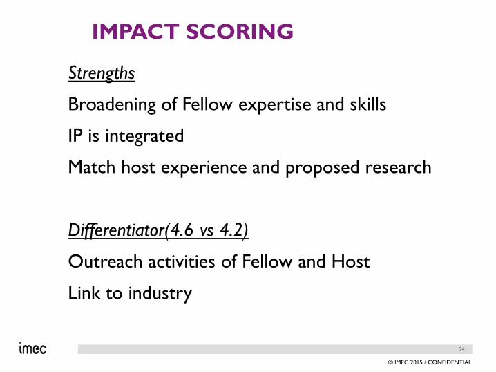
IMPACT SCORING
Strengths
Broadening of Fellow expertise and skills
IP is integrated
Match host experience and proposed research
Differentiator(4.6 vs 4.2)
Outreach activities of Fellow and Host
Link to industry

25
© IMEC 2015 / CONFIDENTIAL
The host has outstanding infrastructure which matches perfectly with this
project.
- The research environment is very stimulating and international.
- The host and collaborating industrial partners are experienced and
collaboration with them will certainly be beneficial to the fellow.
• Build on your strengths
• Build on your institute
• Build on your expertise
• Build on your industrial partnerships

26
© IMEC 2015 / CONFIDENTIAL
GENERAL COMMENTS
Write proposal with the list of questions to the
reviewers in mind.
Create transparent answer to ALL questions▸ Excellence
▸ Impact
▸ Implementation

27
© IMEC 2015 / CONFIDENTIAL
YOU NEED SOME STATISTICAL LUCK WITH REVIEWERS.
• Acquiring experimental experience by hands on
training in operating the high-energy accelerator
and the various experimental end-stations at imec.
It is the aim that, through daily experience, the
researcher will be able to supervise and lead an
accelerator lab independently. (WP1)
• - Acquiring a fundamental understanding of the
underlying physics of charge exchange processes
upon medium energy ion scattering (WP4)
• - Establishing proficiency in optimized data
analysis based on acquired insight into the
physics of the two-dimensional energy/position
spectra through intense collaboration with the
imec researchers (WP4)
• Establishing proficiency in coincidence data
mining processes to optimize the extraction of
information (WP4)
• - Establishing proficiency in leading and
organizing a major project of development. (WP2)
• - The researcher will (re-)establish a solid network
of collaboration in the ion beam analysis
community (WP2). The researcher will also be
exposed to the needs and the dynamics of the
micro-electronics research community.
• be exposed to the way-of-working in an industrial
research environment, and he will understand
• Building experimental experience by
hands on training in site selective
sample preparation and tip shaping
based on FIB, (WP1)
• Acquiring a fundamental knowledge
related to the underlying physics of the
laser assisted evaporation process by
working alongside imec’s APT-team
and its theoreticians (WP2)
• Establishing proficiency in optimized
data generation based on acquired
insight into the physics of the tip shape
evolution and the parameters
controlling it (WP3)
• Establishing proficiency in correlative
data reconstruction (APT-TEM
tomography) through interaction with
Imec and its collaborators. (WP4)
• Acquire knowledge of advanced
technology from device engineers
through case studies linking APT-
results with device development (WP
5)
Prop 1 Strengths : Transfer-of-
knowledge objectives closely match the
project work packages.
Prop 2 :Weakness : There is no
program of formal technical training4.4 4.7