Embed Size (px)
Citation preview
Atomic-Scale Analysis of the SiC/Oxide Interface to Improve High-Power MOSFET Devices
Inauguraldissertation
zur
Erlangung der Würde eines Doktors der Philosophie
vorgelegt der
Philosophisch–Naturwissenschaftlichen Fakultät
der Universität Basel
von
Dipanwita Dutta
aus Kolkata, India
Originaldokument gespeichert auf dem Dokumentenserver der Universität Basel https://edoc.unibas.ch

i
Genehmigt von der Philosophisch-Naturwissenschaftlichen
Fakultät auf Antrag von:
Prof. Dr. Thomas Jung
Prof. Dr. Ernst Meyer
Basel, 21.05.2019
Prof. Dr. Martin Spiess
Dekan


Dedicated
To
My Beloved Parents,
to their selfless affection and inspiration...

ii
Acknowledgements
During the four year period of my PhD I had the fortune to collaborate with multinational companies
as well as world renowned research institutes. My thesis is an outcome of this four years’ work and I
am grateful to everyone who significantly contributed professionally or personally towards
overcoming any challenges arising during this time. I thank you all for imparting the true value of
optimism on me and making my research life enjoyable.
Firstly, with my deepest gratitude I would like to acknowledge my mentor and research supervisor
Professor T. A. Jung for letting me work in his group. His thinking and selfless dedication nourished
me in understanding crucial problems in the early stage of my research. I am also grateful to him, for
suggesting such riveting projects to work on. His advices on research and career are invaluable.
I would like to thank the Swiss National Science Foundation for their financial support and the Swiss
Nanoscience Institute (SNI) for giving me the opportunity to do my research in a prestigious institute
under the guidance of eminent professors (project no. A10.08 Atolys). I acknowledge the support
from University of Basel and Paul Scherrer Institute. Especially the valuable discussions with
professors during this time of my stay and the knowledge they imparted on me. A special thanks to
Prof. Dr. Jens Gobrecht. Apart from being adept, his omnicompetent personality stimulates and
motivates people of all ages and fields.
I would like to thank Dr. Hans Sigg and Prof. Ulrike Grossner for the discussions on my project. Also
a special thanks to Dr. A. Schoener from Ascatron for providing the MOS capacitors, R. Schelldorfer
for solving the difficulties with AFM, Dr. Daniel Fan for Raman measurements and summer student
P. Davenport for his contribution in data analysis.
Constant assistance and the friendly nature of the technical staff helped me doing my experiments
smoothly. Here I would like to acknowledge the clean room experts Dr. Martin Bednarzik, Dario
Marty, also Stefan Stutz and Anja Weber for the in-house SEM. A special thanks to Dr. Elisabeth

Müller for her patience and constant source of help during FIB and TEM measurements in PSI. I
would like to show my appreciation to the theory collaborator from Uni Basel in Prof. Stefan
Goedecker’s group. Apart from Dr. Deb Sankar De and Dr. Shantanu Roy, Prof. Goedecker himself
has been available providing his expertise in the field any time necessary.
I am grateful to all the help I obtained from the scientists from ETHZ and Jülich forschungszentrum
while performing my experiments there. I am thankful to Dr. Alla Sologubenko from ETHZ who
never failed to help me with STEM and for hours of valuable discussions; also Dr. Stephan Gerstl for
the LEAP facility at ETHZ. I am indebted to the help I received from Doris Meertens from Jülich for
the FIB/Nanomill support and Marc Heggen and Paul Paciock for the TITAN and Chemi STEM
support. I am gratified because of the collaboration I had with ABB and thankful for the numerous
meetings I had with Prof. Jörg Lehmann and Dr. Giovanni Alfieri who never failed to drive me with
ambition and optimism. Also I appreciate Dr. Holger Bartolf for his valuable input towards the
success of the project. I shall not forget the guidance and contributions from Corrado Bongiorno from
CNR Italy regarding the in-depth understanding of STEM/EELS analysis.
I am also grateful to my fun filled and helpful colleagues Dr. Harald Rossmann, Dr. Jan Nowakowski,
Dr. Milos Baljozovic, Dr. Massimo Camarda, Judith Wörle for their valuable inputs on past and
present experience in research life. My hearty thanks to all my friends Daniel, Adrienn, Vassia,
Matthias, Aisha, Manolis, Yve thanks to you all for the joyous time we spent. I would like to show
my gratitude to Prof. Kulkarni and Prof. C.N.R. Rao for always being a source of inspiration for me. I
also acknowledge Christian’s (Hitch’s) contribution towards my thesis. A special thanks to Jan
Schaab for being a constant support in difficult times and for always seeing the best in me.
Lastly, I would like to acknowledge the most important people of my life, my parents and mama (my
late uncle). Without their love and encouragement all my efforts would have gone to vain. My
parents’ endearing support has been the backbone for what I am today and what I will be in the
future. I am grateful to them for whatever they gave me and I dedicate my thesis to them.

iv
Preface
The world-wide effort to curb the emission of green-house gases has led to an increased push for
technologies for the highly efficient generation, transportation and utilization of electrical power.
Semiconductor-based inverters for example, are needed to connect photovoltaic arrays to the power grid,
enable transport of the electrical energy over large distances and allow the energy-efficient control of
electrical motors. To this date, silicon based power devices cover a wide range of such applications.
However, SiC if used will enable higher switching speeds at simpler system topologies. This will enable
in a reduction of overall system and material cost as well as higher efficiency and reliability. Although
SiC has been studied since long it is only recently that the substrate quality, size and manufacturing
capabilities are becoming mature enough to enable a reliable large-scale production of power electronic
devices with acceptable performance and yield. Wafers with reasonable defect density and sizes up to 6
inches are now available boosting the manufacturing of SiC power devices, mainly unipolar diodes, by
large global companies. SiC MOSFETs, in turn, have not unfolded their full potential yet because of the
challenges associated with the formation of a high quality gate oxide from SiC.
Within the scope of this dissertation the atomic structure and the electronic properties of the silicon-
carbide silicon-dioxide (SiC/SiO2) interface has been discussed and investigated, motivated by its great
importance for high power semiconductor devices. This work gears at the scientific understanding of the
structure-property relationship of the gate oxide interface and aims towards identifying a manufacturing
procedure to reduce the defect-levels near the interface as they are currently compromising carrier
channel mobility in SiC-MOS devices. The content has been organized in chronological order according
to the development of the research project. After briefing on the problem and the methods used for my
work, the thesis will consist of two main parts. The first one reports about the identification of defects in
general and specifically C-defects on the atomic scale and the second one is concerned about how the
interface defects can be curtailed using passivation. The project has been a part of the “Nano-Argovia”
programme of the Swiss Nanoscience Institute (SNI) and has been investigated in close collaboration of
the Laboratory of Micro and Nanotechnology (PSI) with the Department of Physics (University of Basel)
as the academic partner and ABB’s Corporate Research Center as the industrial partner.

v
Abstract
“The history of solid-state physics in general and of semiconductors in particular,
is not so much about great men and women and their glorious deeds,
as about the unsung heroes of thousands of clever ideas and skillful experiments
—reflection of an age of organization rather than of individuality.”
— Ernest Braun
This thesis entitled “Atomic-Scale Analysis of the SiC/Oxide Interface to Improve High-Power
MOSFET Devices” aims at a technology innovation critical for stepping up the energy efficiency in
advanced silicon carbide (SiC) based metal oxide semiconductor field effect transistors (MOSFET) for
high power semiconductor technology. While the wide band gap, high thermal conductivity, and high
saturation velocity are very desirable, SiC has a major disadvantage in comparison with Si or gallium
arsenide (GaAs). Compared to state-of-the-art silicon technology, the channel mobility in SiC MOSFETs
is very low compared to the bulk mobility and is strongly dependent on its crystallographic orientation
and the interface.
In contrast to Si where the passivation of surface states due to the SiO2 layer was a breakthrough, the
more complex nature of the oxidation process is still hampering such developments in SiC. It remains a
pestering question, even after decades of intensive R&D, which kind of defects degrade the near-
interface mobility of SiC-MOS devices and whether and how the proposed carbon clusters could be
involved.
This thesis comprises a new approach in that multiple experimental techniques are combined with
minima-hopping density functional theory for atomistic simulations and property prediction. It is by the
iterative multi-technique investigation of structures, properties and processes down to the atomic level
vi
that in-depth understanding of complex phenomena and mechanisms occurring at the interface during
oxidation can be inferred.
In the present thesis spectro-microscopy and theory investigations have been used to investigate defects in
particular C-defect formation during the fabrication of thermal oxides on SiC. The presence of carbon
defects at this interface affecting the near interface channel mobility are consistently evidenced i) by a
wide range of starting conditions in Density Function Theory and Monte Carlo simulations, and most
importantly ii) by in-depth high resolution secondary transmission electron microscopy, EELS and
Raman spectra iii) by few of the first Local Electrode Atom Probe (LEAP) experiments performed on
SiC/SiO2 interface samples and iv) by the most recent high resolution STEM data obtained by us allowing
for in-depth analysis of the defect structure in addition to modelling, defect spectroscopy and transport
measurements.
The thesis has been allocated into six chapters. Chapter I introduces SiC as a semiconducting material
and its usefulness in power devices. It also briefly establishes the origin and role of various defects at the
interface towards reducing the channel mobility. In Chapter II we get an overview of how C as a defect
has been a controversial topic for decades and unveils the various methods and techniques we have been
using in order to detect this C-nucleates. Chapter III explains how the sample preparation plays a very
important role in order to achieve high-resolution data. Also here, we describe how different samples are
prepared for different experiments: AFM measurements required removal of oxide using an etching
solution in order to gain morphological information of the interface. FIB has been used to mill thin
lamellae and pillars for HRTEM and LEAP experiments respectively. Chapter IV pertains to the
atomistic analysis in order to find the C-defects at the interface. Using AFM we perceived the architecture
of SiC interfaces and consolidated the speculations of C-nucleates being present at the interface. In order
to gain knowledge about the various chemical bonds present at the interface we used Raman
spectroscopy. HRTEM and LEAP proved that there are also dangling bonds along with stoichiometric
dislocations at the interface leading to a broadening of the interface via the imperfect layer by layer
oxidation and the penetration of defects into the SiC resulting in deterioration of the channel mobility.
EELS and STEM analysis revealed the exact positions at which the C-defects are present and where they
are attached to the interface. After reporting the concerting evidence of C-nucleates as defects in chapter
IV, the following Chapter V deals with passivation and interface treatment methods; and on their
potentially beneficial influence on near interface defect densities and electronic properties. Finally, in
Chapter VI we conclude our thesis with the final results we obtained and provide an outlook towards
future investigations and what is to be done next.

vi

vii
Table of Contents
Declaration ....................................................................................................................................... i
Acknowledgements ......................................................................................................................... ii
Preface ............................................................................................................................................ iv
Abstract ............................................................................................................................................v
Table of Content ........................................................................................................................... vii
List of Acronyms ........................................................................................................................... xi
Chapter I: Overview of SiC as a high power semiconductor device material
I.1 Introduction ................................................................................................................................1
I.2 Properties of SiC making it unique for high power devices .......................................................2
I.3 Importance of gate oxide and interface for high power devices .................................................4
I.4 Defects in SiC-MOSFETs ..........................................................................................................6
I.5 History on studies of different defects in SiC MOS-devicess ....................................................7
I.6 Inference ....................................................................................................................................8
viii
Chapter II: Carbon defects in SiC/SiO2 interface and techniques used for their detection
Summary ...................................................................................................................................9
II.1. Introduction .....................................................................................................................10
II.2 Scope of Investigation ......................................................................................................11
II.3 Methods and techniques to detect C-defects ....................................................................11
II.3.1 Atomic Force Microscopy (AFM) .........................................................................12
II.3.2 Raman Spectroscopy ..............................................................................................12
II.3.3 Focused Ion Beam ...................................................................................................13
II.3.4 Scanning/ Transmission Electron Microscopy .......................................................15
II.3.5 Local Electrode Atom Probe ..................................................................................17
II.3.6 Theoretical Simulation ...........................................................................................18
II.4 Inference ............................................................................................................................18
Chapter III: Sample preparation TGO/pTGO
Summary .................................................................................................................................20
III.1 Introduction .....................................................................................................................21
III.2 Scope of Investigation .....................................................................................................22
III.3 Sample Preparation .........................................................................................................22
III.3.1 Samples for AFM and Raman...............................................................................23
III.3.2 Samples for S/TEM ..............................................................................................24
III.3.3 Samples for LEAP ...............................................................................................25
III.3.4 Samples for theoretical simulations ......................................................................25
III.4 Inference .........................................................................................................................26
Chapter IV: Atomic analysis of SiC/SiO2 interface to find C-defects
Summary .................................................................................................................................27
IV.1 Introduction .....................................................................................................................28
IV.2 Scope of Investigation ....................................................................................................28
IV.3 Results and Discussions ..................................................................................................29
IV.3.1 Visualizing the C-defects at the interface .............................................................29
IV.3.2 Chemical analysis of unwanted C-bonds at the interface .....................................32
IV.3.3 Density of State for C-defects near the band gap .................................................37
IV.3.4 3D chemical imaging of the C-nucleate ...............................................................41
IV.3.5 Chemical imaging to understand the position and size of the C-defects ..............45
IV.4 Inference ..........................................................................................................................52
Chapter V: Relevant parameters for improving thermally grown gate-oxide interface
Summary .................................................................................................................................53
V.1 Introduction ......................................................................................................................54
V.2 Scope of Investigation ......................................................................................................54
V.3 Results and Discussions ...................................................................................................55
V.3.1 Visualizing and characterization of the interface after ozone treatement ..............55
V.3.2 Visualizing the interface after N2Otreatment/passivation ......................................58
V.4 Inference............................................................................................................................62
Chapter VI: Conclusion and Outlook
Summary .................................................................................................................................64
VI.1 Conclusions and Discussions ..........................................................................................65
VI.2 Outlook ...........................................................................................................................69
Bibliography ...........................................................................................................................73
Curriculum vitae ......................................................................................................................81

xi
List of Acronyms AFM
HR-S/TEM
LEAP
EELS
MOSFET
DOS
DFTB
MHM
APT
FIB
HAADF
EDX
TOF
NIT
P/TGO
I/FFT
SEM
Atomic Force Microscopy
High Resolution- Transmission Electron Microscopy
Local Electrode Atom Probe Tomography
Electron Energy Loss Spectroscopy
Metal Oxide Semiconductor Field Effect Transistor
Density of State
Density Function Theory Tight Binding
Minima Hopping Method
Atom Probe Tomography
Focused Ion Beam
High-Angle Annular Dark-Field
Energy-Dispersive X-ray Spectroscopy
Time of Flight
Near Interface Traps
Passivated/Thermally Grown Oxide
Inverse/ Fast Fourier Transform
Scanning Electron Microscope

Chapter I
Overview of SiC as a high power semiconductor device material
“It was not so very long ago that people thought that semiconductors were part-time
orchestra leaders and microchips were very small snack foods.”
Geraldine Ferraro
I.1 Introduction
The sustainable supply and efficient conversion of energy is of major concern in today’s society and
economy and the semiconductor industry plays a pivotal role that commuted the world without a
doubt. The birth of semiconductor devices can be traced back to 1874 1 when C.F. Braun who was
that time conducting research on metal sulfide conductivity invented the rectifier as AC-DC
converter. The semiconductor industry continued to flourish following the invention of the junction
transistor by Shockley in 1948 for which he was awarded the Nobel Prize in Physics in 1956.2 In 1957
Overview of SiC as a high power semiconductor device material Chapter I
2 | P a g e
the industry already grew to a scale of 100 million dollars. In parallel, this was the dawn for power
electronics.3 Power electronics is a division of solid state electronics where high-efficiency switches
convert and control electrical power for a wide range of applications. This includes the operation of
electrical supply grids with decentralized renewable energy sources, i.e. wind, small scale water and
solar power plants. Other applications of power electronics includes traction control, recuperation for
electric and diesel electric engines and for ships, as well as hybrid and electrical drive trains.4 Thus,
power electronics can save enormous usage of fossil energy in automotive technology. Currently, we
can designate the 21st century to be the golden age of power electronics applications because of the
evolution of technology leading to major innovations like FET-plus-driver modules, power supplies
with best integrated circuit designs and transformers. 5-6
Solid-state electronics originally started with Ge, but it gradually transformed to using Si as its base.
Si quickly became the material of interest since it has larger band gap which prevents leakage currents
when the device is in the OFF-state. This is suitable for power applications giving rise to the Si age.
Another important reason for Si being popular is because of the high quality oxide/semiconductor
interface. This is due to the passivating nature 7 of SiO2 on the surface states which is important in
Metal-Oxide-Semiconductor (MOS) systems. However, Si has its limitations in current high power
applications. A high critical electric field is required in a device operating in high frequency and high
temperature to withstand large breakdown voltages during the operation of the device in reverse
direction. Hence, even wider bandgap materials than Si are desirable and scientists have been looking
for materials with favorable properties, despite the success of Si. For these reason compound
semiconductors belonging to the III-V compound groups gained more recognition.8
I.2 Properties of SiC making it so unique for high power devices
Power applications require high critical electric field (Ec) to withstand large breakdown voltages and
materials with a wider bandgap than Si are more suitable. In contrast to silicon (Si) and GaAs, SiC
exhibits a wide band gap of 3.2 eV (1.1 eV in Si and 1.43 in GaAs) and a high critical electric
breakdown field of above 2.2MV/cm (10 times higher than Si and GaAs). This makes SiC one of the
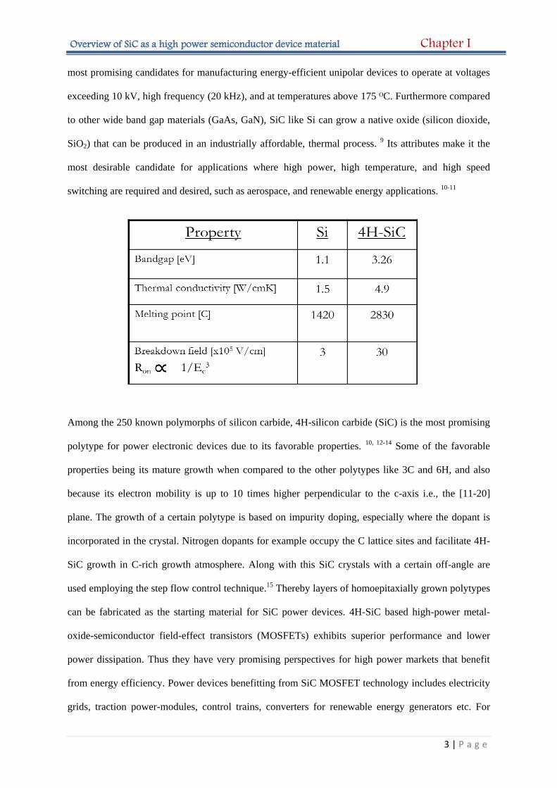
Overview of SiC as a high power semiconductor device material Chapter I
3 | P a g e
most promising candidates for manufacturing energy-efficient unipolar devices to operate at voltages
exceeding 10 kV, high frequency (20 kHz), and at temperatures above 175 ᴼC. Furthermore compared
to other wide band gap materials (GaAs, GaN), SiC like Si can grow a native oxide (silicon dioxide,
SiO2) that can be produced in an industrially affordable, thermal process. 9 Its attributes make it the
most desirable candidate for applications where high power, high temperature, and high speed
switching are required and desired, such as aerospace, and renewable energy applications. 10-11
Among the 250 known polymorphs of silicon carbide, 4H-silicon carbide (SiC) is the most promising
polytype for power electronic devices due to its favorable properties. 10, 12-14 Some of the favorable
properties being its mature growth when compared to the other polytypes like 3C and 6H, and also
because its electron mobility is up to 10 times higher perpendicular to the c-axis i.e., the [11-20]
plane. The growth of a certain polytype is based on impurity doping, especially where the dopant is
incorporated in the crystal. Nitrogen dopants for example occupy the C lattice sites and facilitate 4H-
SiC growth in C-rich growth atmosphere. Along with this SiC crystals with a certain off-angle are
used employing the step flow control technique.15 Thereby layers of homoepitaxially grown polytypes
can be fabricated as the starting material for SiC power devices. 4H-SiC based high-power metal-
oxide-semiconductor field-effect transistors (MOSFETs) exhibits superior performance and lower
power dissipation. Thus they have very promising perspectives for high power markets that benefit
from energy efficiency. Power devices benefitting from SiC MOSFET technology includes electricity
grids, traction power-modules, control trains, converters for renewable energy generators etc. For

Overview of SiC as a high power semiconductor device material Chapter I
4 | P a g e
these reasons, mature SiC power devices have been manufactured in relatively high-batch volumes
during the last decade by several corporations (GE, Cree, Mitsubishi, Infineon, Rohm, etc.), with a
market volume predicted to grow up to 38% a year up to 436 M$US in 2020.16
Predicted impact SiC will make:
Hybrid vehicles will benefit from a 10% extended driving range.
Airplanes will benefit from a reduction of weight by at least 1000 lbs with more compact high
efficiency power systems
In medical imaging smaller, more efficient systems will be introduced, saving floor space and
energy, towards lower healthcare cost.
In data centers, the fastest growing segment of electricity consumption, more than 5% energy
savings will be possible.
Renewable sources of energy can be harnessed more efficiently because of a reduction of
wasted power in decentralized grids by 50%.
Calculations predict that SiC if used in current devices in high power systems will save one year’s
worth energy of the canton of Bern and Valais for whole Switzerland.17
I.3 Importance of the Gate-Oxide (SiO2) and SiC/SiO2 interface for High Power Devices
In MOSFETS, the gate electrode is separated by a thin insulating layer from the semiconductor in
which it controls the formation of a conducting channel. Planar, atomically well-defined (~ 10 nm-40
nm) gate insulator layers in nanometer-close proximity (<25 nm) and defect-free semiconducting
channels are required to sustain a high carrier mobility and gate-oxide reliability.
If the ‘bulk’ thermal oxide grown on SiC is compared to that grown on Si there is no evidence of
difference in their properties. SiC oxidation also yields stoichiometric SiO2 whose refractive index, 18
and breakdown field are similar to the Si thermal oxides.19 However, though SiC can be thermally
oxidized to yield SiO2 over its surface, a fundamental inherent drawback of SiO2 is its low dielectric
Overview of SiC as a high power semiconductor device material Chapter I
5 | P a g e
constant, which is about 2.5 times lower than that of the SiC material and also the poor interface
properties at the SiO2/SiC junction. This leads to a proportionally larger electric field enhancement in
the SiO2 dielectric compared to the SiC semiconductor layer underneath. This is the reason why new
dielectrics with dielectric constants at least similar to that of the SiC and with lower interface state
densities might be required for device applications. Note that these inequalities of dielectric constant
often requires device operation at an electric field far below the SiC material breakdown field in order
to avoid premature SiO2 breakdown at the device surface. A variety of oxidation methods has been
developed, such as thermal oxides, deposited oxides, hybrid oxides and alternate dielectrics. For each
of these oxidation processes various subprocesses exist, each with its advantages and disadvantages.5
Also, due to the 10 times larger critical field in SiC compared to Si power devices, the oxide is under
significant electrical stress in conventional designs.
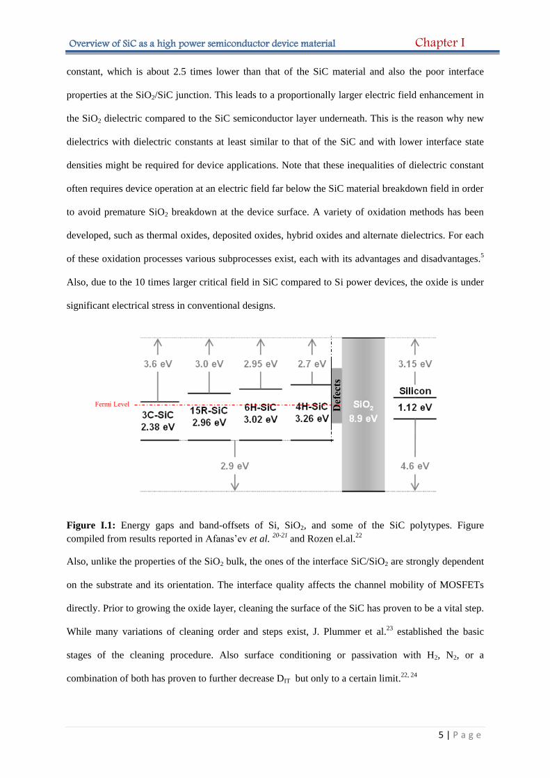
Figure I.1: Energy gaps and band-offsets of Si, SiO2, and some of the SiC polytypes. Figure
compiled from results reported in Afanas’ev et al. 20-21 and Rozen el.al.
22
Also, unlike the properties of the SiO2 bulk, the ones of the interface SiC/SiO2 are strongly dependent
on the substrate and its orientation. The interface quality affects the channel mobility of MOSFETs
directly. Prior to growing the oxide layer, cleaning the surface of the SiC has proven to be a vital step.
While many variations of cleaning order and steps exist, J. Plummer et al.23 established the basic
stages of the cleaning procedure. Also surface conditioning or passivation with H2, N2, or a
combination of both has proven to further decrease DIT but only to a certain limit.22, 24
Fermi Level
Def
ects
Overview of SiC as a high power semiconductor device material Chapter I
6 | P a g e
I.4 Defects in SiC-MOSFET
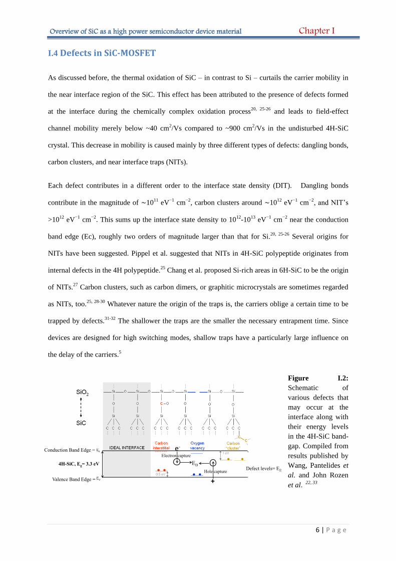
As discussed before, the thermal oxidation of SiC – in contrast to Si – curtails the carrier mobility in
the near interface region of the SiC. This effect has been attributed to the presence of defects formed
at the interface during the chemically complex oxidation process20, 25-26 and leads to field-effect
channel mobility merely below ~40 cm2/Vs compared to ~900 cm2/Vs in the undisturbed 4H-SiC
crystal. This decrease in mobility is caused mainly by three different types of defects: dangling bonds,
carbon clusters, and near interface traps (NITs).
Each defect contributes in a different order to the interface state density (DIT). Dangling bonds
contribute in the magnitude of ∼1011 eV−1 cm−2, carbon clusters around ∼1012 eV−1 cm−2, and NIT’s
>1012 eV−1 cm−2. This sums up the interface state density to 1012-1013 eV−1 cm−2 near the conduction
band edge (Ec), roughly two orders of magnitude larger than that for Si.20, 25-26 Several origins for
NITs have been suggested. Pippel et al. suggested that NITs in 4H-SiC polypeptide originates from
internal defects in the 4H polypeptide.25 Chang et al. proposed Si-rich areas in 6H-SiC to be the origin
of NITs.27 Carbon clusters, such as carbon dimers, or graphitic microcrystals are sometimes regarded
as NITs, too.25, 28-30 Whatever nature the origin of the traps is, the carriers oblige a certain time to be
trapped by defects.31-32 The shallower the traps are the smaller the necessary entrapment time. Since
devices are designed for high switching modes, shallow traps have a particularly large influence on
the delay of the carriers.5
Figure I.2:
Schematic of
various defects that
may occur at the
interface along with
their energy levels
in the 4H-SiC band-
gap. Compiled from
results published by
Wang, Pantelides et
al. and John Rozen
et al. 22, 33
Conduction Band Edge =
Valence Band Edge =
e-
+
4H-SiC, Eg= 3.3 eV EDDefect levels= ED
Electron capture
Hole capture
Overview of SiC as a high power semiconductor device material Chapter I
7 | P a g e
I.5 History on studies of different defects in SiC MOS-devices
Shallow interface traps with energy levels just below the conduction band were held responsible for
the low channel mobility of the thermally grown SiC/SiO2 interface.5 But based on newer
observations, it was concluded that defects responsible for low mobility were physically located near
the interface; most recently it has been established by considering quantum confinement effect, that
the active NIOTs are energetically located above the bottom of the conduction band and physically
located very close to the interface with short response times.34 Imperfections and defects near the
interface were identified utilizing electrically detected magnetic resonance evidencing for significant
disorder at the interface35-36 High-resolution Rutherford backscattering spectroscopy analysis together
with cathode luminescence (CL) spectroscopy and TEM suggested that the deviations of
stoichiometry and roughness at the interface, defined the effects of the interface of SiO2/4H-
SiC(0001).37 Investigations in order to solve the confusion and understand the active defects and
NIOTs and how to passivate them are still going on. For a decade SiC thermal nitridation followed by
oxide deposition provided a route to confine nitrogen at the SiO2/SiC interfacial region which
improved the channel mobility. To investigate the effects of nitrogen it has been incorporated into SiC
by annealing in isotopically enriched ammonia. Electrical measurements on such MOS structures
revealed poor electrical quality suggesting nitrogen incorporation at the interface has to be done in a
very specific manner in order to improve the mobility. 22 Similarly NO and forming gas post oxidation
annealing treatments on the interfacial properties were investigated and revealed that forming gas
annealing has limited effect on the interface trap density (Dit). It results however, in an improvement
of the insulating properties of thermal oxide. On the other hand, NO annealing causes a drastic
reduction in Dit across all energy levels, but the reliability of the device is not very effective. Hence a
combined treatment leads to a significant reduction in interface trap density and uniform reliability.22
Recent reports on passivation techniques reveals that POCl3, Ba or N introduce significant changes to
the near-interface atomic structure of SiC at SiC/SiO2 interface but the reason and the mechanism
behind the passivation is not clear.4 In literature constant capacitance deep level transient
spectroscopy (CCDLTS) measurements reveals an electron trapping reduction by a factor of 2 at
Overview of SiC as a high power semiconductor device material Chapter I
8 | P a g e
energy levels within 0.2 eV of the SiC conduction band edge by using Sb at the SiO2/SiC interface
which improves the channel mobility of the MOSFETs.38-39 Theoretical studies on such systems have
been performed for decades by modelling pair of edge dislocations using ab initio methods. Such
results disclose that (i) the crystal structure is strongly disturbed in the small vicinity of the dislocation
core, (ii) additional energy levels present in the energy gap originate from the atoms with broken
bonds in the neighborhood, (iii) spatial tunnels exist, with atoms creating localized states in the band
structure and significantly decreasing electrostatic barriers. The later should be considered as one of
the primary factors responsible for experimentally observed reduction of the breakdown voltage.10
I.6 Inference
The defects at the interface create localized energy levels in the band-gap (which will be discussed in
details in chapter IV) leading to enhanced Coulomb scattering thus reducing the carrier lifetime. The
channel mobility of SiC MOS devices is therefore lowered to a fraction of its bulk value. The shallow
states close to the conduction band edge of 4H-SiC are caused by near-interface defects and C-related
defects. Their presence may provide an explanation for the trap levels within the rest of the band-gap.
The origin and physical nature of these defects especially C-defects and their effect as carrier traps
have been the subject of intense research. This has also been the topic investigated in this thesis with
particular focus on C-related defects, their identification and the historic evolution of evidences found
to support their presence.

Chapter II
Carbon defects in SiC/SiO2 and techniques used for
their detection
“One of the basic rules of the universe is that nothing is perfect. Perfection simply doesn't
exist.....Without imperfection, neither you nor I would exist”
Stephen Hawking
Summary
Defects occur near the gate insulator/semiconductor interface due to the more complex nature of the
oxidation process which requires removal of carbon atoms in the form of CO and CO2 from the SiC
crystal. In this chapter we introduce the different forms of carbon defects at and near the interface and
the techniques used in my work solely for the purpose of identifying the relevant C-defects
compromising the near interface SiC channel mobility.
Carbon defects in SiC/SiO2 and techniques used for their detection Chapter II
10 | P a g e *Theoretical simulation performed by Prof. Goedecker et al. in Uni Basel.
II.1 Introduction
The excess carbon from the SiC crystal during the complex oxidation process causes various types of
specific defects in the near interface region and in the oxide. These not only modify the electronic
properties of the inversion channel, but also deteriorate the field-effect channel mobility and introduce
scattering centers for the charge carriers, thereby increasing the interface trap density. The physical
origin of the Near Interface Traps (NITs) remains unclear, but recent studies suggest the formation of
carbon clusters, such as carbon dimers, or graphitic microcrystals at the interface.25 Experimental
evidence of their presence has been concluded from atomic force microscopy (AFM) studies of SiC
surfaces after the oxide removal.20, 40 However, it is also reported that there is no graphite layer
exceeding 0.1 monolayer based on in situ XPS studies.25, 41 So according to the different reported
studies carbon clusters were not directly observed at the SiO2/SiC interfaces but measurements
indicate that if present they would be a few atoms in size. In case such small C-nucleates/ clusters
exist, the corresponding energy levels would be dependent on the environment of the clusters, which
has not been considered in most of the reports before.22
Therefore theoretical simulations of the interface are very useful as a complementary tool. Using
simulation we can learn about defects in the form of C-clusters (also C-nucleates) and their trap
levels. Extensive work has been performed using density-functional theory (DFT) but it is unable to
reproduce the real values of the band gaps of the semiconductor.42 Thus the calculated energy levels
may not be 100% accurate. Also, as described before the energy of a defect relies on its surrounding
solid matrix where it is embedded. Accordingly the calculated values for each of the cluster-in-matrix
configurations will correspond to specific cases. Moreover, the theoretical work done so far
considered the kinetics during the oxidation only to a limited extent as it only considers a static
interface, where oxide is placed on the interface instead of being grown using unbiased techniques, for
the defect identification. Hence, the theoretical results so far provided a broad knowledge of possible
C-defects and their impact, without much confirmation.
Carbon defects in SiC/SiO2 and techniques used for their detection Chapter II
11 | P a g e *Theoretical simulation performed by Prof. Goedecker et al. in Uni Basel.
Our current work goes beyond previous work in that it links extensive experimental results using
different techniques to advanced DFTB simulations of the oxidation process to understand the
formation of carbon defects and further characterize their atomistic structure.
II.2 Scope of Investigation
Buried interfaces generally impose challenges limiting the investigation of local structure and material
properties which compromise the use of e.g. diffraction techniques and require challenging and
careful sample preparation procedures even if e.g. well established microscopy techniques like
Scanning Electron Microscopy (SEM) and Transmission Electron Microscopy (TEM) are to be
applied.
From the theoretical point of view several researchers came up with methods to perform structure
predictions as discussed in the introduction above. The Minima Hopping method developed in the
group of Goedecker goes beyond previous DFT methods in that the absolute minimum structure can
be identified with high reliability. Thus we are able to use some of the latest and most advanced
simulation tools that are not yet widely available to study industrially relevant properties in silicon-
carbide based electronic devices.
II.3 Methods & techniques to detect C-defects
The wide spectrum of microscopic and structural investigation techniques (Optical Microscopy,
Scanning Electron Microscopy, (Scanning) Transmission Electron Microscopy, Atomic Force
Microscopy) shall be complemented with chemical and structural investigations with light (Raman
spectroscopy) and atom probe tomography. Thereby, macroscopically measured values, like the
break-down electric field shall be related to the presence of impurities, defects and also to the crystal
and grain structure defect. In parallel to these structural investigations of near interface defects at the
atomic scale, numerical simulations on MOSFET architectures shall complement the obtained
experimental results.
Carbon defects in SiC/SiO2 and techniques used for their detection Chapter II
12 | P a g e *Theoretical simulation performed by Prof. Goedecker et al. in Uni Basel.
II.3.1 Atomic force microscopy (AFM):
Atomic force microscopy is a high-resolution imaging technique, specific form of scanning probe
microscopy where a small probe with a sharp tip (3-6 um tall; 15-40 nm end radius) is scanned back
and forth in a controlled manner across a sample to measure the surface topography at an atomic
resolution (lateral resolution ~30nm and vertical resolution 0.1nm). PeakForce Tapping is an AFM
technique that enables the highest resolution surface imaging along with highly sensitive nanoscale
property mapping.
AFM measurements were conducted in air with a Bruker AFM (Dimension ICON with ScanAsyst).
AFM was used in tapping mode to assess the morphology of the specimens at different stages. The
NanoScope processing software was used, and samples were typically investigated on different scales
ranging from 5 µm down to 100 nm; the noise threshold was set to 0.01 nm and the Z range was fixed
to 1 µm.
II.3.2 Raman:
Raman spectroscopy is used for studying low frequency modes like vibrational and rotational modes.
Raman is a scattering phenomenon. It depends on inelastic scattering of photons by phonons and thus
on polarization changes. So Raman always needs a source for polarizing the molecule. Again this
polarisability is a function of interatomic distance making Raman spectrum sensitive to small changes
in the local bond lengths, bond angles to provide unique information about molecular morphology.43
• D band: It is known as the defective band. The breathing motion of six atom rings gives rise
to this band. A defect is required for its activation to be visible in the Raman signal. This involves
phonons of the k (k is the wave vector for the electronic transition) zone boundary of the brillouin
zone. The phonon mode which satisfies the condition k=q/2 (q is the phonon wave vector) is the
origin of the D peak with A1g symmetry. Its position is at 1350 cm-1 and changes with excitation
energy. The D band reveals the disorders in the electronic structure such as defects, grain boundaries,
and functional groups in the sp2 carbon lattice.
Carbon defects in SiC/SiO2 and techniques used for their detection Chapter II
13 | P a g e *Theoretical simulation performed by Prof. Goedecker et al. in Uni Basel.
• G band : It is named as the graphitic band. The in-plane bond stretching of sp2 carbon atoms
gives rise to this band. The G band position is at 1580 cm-1. Here the zone center phonons instead of
the zone boundary phonons, with E2g symmetry are required for its origin. Dispersion being
proportional to the degree of disorder, the G band disperses more when the degree of the defect or
disorder is high.
For experiments in the SiC/SiO2 specimen a home-built micro Raman spectroscopy setup based on a
532 nm single mode continuous wave laser and an inverted microscope (Leica DM5000 equipped
with a 100x NA=0.9 objective, Germany) as the sample stage was used. The laser power on the
sample was measured to be 0.75 mW. The scattered light passed through a 532 nm long pass Raman
filter (Semrock, Rochester, U.S.A.) with 40 µm slit and onto a 600 lines/mm grid spectrograph (Acton
SP500i, Princeton Instruments, U.S.A.). A CCD camera (ProEM 1600^2, Princeton Instruments,
U.S.A.) was used as the detector. Raman peaks were fitted using Lorentzian lineshapes (OriginPro,
OriginLab, U.S.A.). The spot size for the green laser is ~2.3 µm.
II.3.3 Focused Ion Beam:
Focused ion beam (FIB) is one of the precise maskless fabrication tools which uses both bottom-up
and top-down fabrication approaches to fabricate complex 3-D micro-/nano-structures with high
precision. FIB instruments can be stand-alone single beam instruments; alternatively, FIB columns
can be incorporated into other analytical instruments such as a scanning electron microscope (SEM),
transmission electron microscope (TEM), or secondary ion mass spectrometry (SIMS). Small probe
(diameter ~ 5 nm) sputtering is facilitated by the liquid metal ion source (LMIS). Gallium is the most
commonly used LMIS for FIB and the reasons are: Low melting point of 29.8 °C and can exist in the
liquid form near room temperature, low volatility/ vapor pressure, relatively unreactive, good vacuum
properties and Ga+ being a heavy ion makes it good for milling. The Ga+ beam is used to scan and cut
the substrate surface in a vacuum chamber. Ga+ beam etching was originally developed for sample
preparation in electron microscopy. The beam of ions "mill" the specimen surface, via the sputtering
process, and this milling can be controlled with nanometer precision. In addition, ion beam assisted
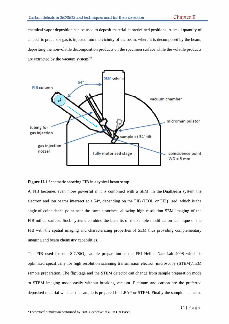
Carbon defects in SiC/SiO2 and techniques used for their detection Chapter II
14 | P a g e *Theoretical simulation performed by Prof. Goedecker et al. in Uni Basel.
chemical vapor deposition can be used to deposit material at predefined positions. A small quantity of
a specific precursor gas is injected into the vicinity of the beam, where it is decomposed by the beam,
depositing the nonvolatile decomposition products on the specimen surface while the volatile products
are extracted by the vacuum system.44
Figure II.1 Schematic showing FIB in a typical beam setup.
A FIB becomes even more powerful if it is combined with a SEM. In the DualBeam system the
electron and ion beams intersect at a 54°, depending on the FIB (JEOL or FEI) used, which is the
angle of coincidence point near the sample surface, allowing high resolution SEM imaging of the
FIB-milled surface. Such systems combine the benefits of the sample modification technique of the
FIB with the spatial imaging and characterizing properties of SEM thus providing complementary
imaging and beam chemistry capabilities.
The FIB used for our SiC/SiO2 sample preparation is the FEI Helios NanoLab 400S which is
optimized specifically for high resolution scanning transmission electron microscopy (STEM)/TEM
sample preparation. The flipStage and the STEM detector can change from sample preparation mode
to STEM imaging mode easily without breaking vacuum. Platinum and carbon are the preferred
deposited material whether the sample is prepared for LEAP or STEM. Finally the sample is cleaned
SEM column

Carbon defects in SiC/SiO2 and techniques used for their detection Chapter II
15 | P a g e *Theoretical simulation performed by Prof. Goedecker et al. in Uni Basel.
and thinned further down using the Nanomill (with Argon Source) from Fischione: Model
1040NanoMill® TEM specimen preparation system.
II.3.4 Scanning/Transmission Electron Microscope:
The scanning transmission electron microscope (STEM) is an invaluable tool for characterizing
nanostructures with the ability to provide information on elemental composition and electronic
structure with the sensitivity of a single atom. The STEM works like a normal scanning electron
microscope (SEM), using a focused electron beam on thin specimens but also has transmission modes
of imaging. Typically, when a field emission gun STEM is equipped with a probe spherical aberration
corrector along with an electron monochromator and a post column energy filter system the resolution
is in the range of sub angstrom.
High-angle annular dark-field (HAADF) imaging is a STEM technique where incoherently scattered
electrons, also known as Rutherford scattered electrons, are used making it highly sensitive to
variations in the atomic mass of the atoms. The HAADF detector thus senses a higher signal from
atoms with a higher atomic number making them brighter in the image. Information about chemical
composition on the nanoscale is pivotal for verifying the architecture of nanostructures and devices,
and X-ray spectrometry is a well-established, robust and easy to use technique to obtain the
comprehensive chemical information. Better yet, in the S/TEM, X-ray analysis pairs microstructural
information obtained from high-resolution imaging with accurate chemical composition information.
Modern X-ray analysis on the S/TEM employs a well-established technology called X-ray energy
dispersive spectroscopy (EDX) that operates in the following manner: The electron beam ejects
atomic core-shell electrons from the sample. The recombination of a higher shell electron into the
now empty core state creates X-rays imprinted with this atom’s characteristic energy. The X-rays
created in the sample are absorbed by a detector and the deposited X-ray energy creates a few hundred
to a few thousand electron-hole pairs, which are immediately separated and collected by the detector
as a charge pulse. The fast electronics to accurately detect these pulses are robust and reliable,
meaning they produce highly-repeatable results that are easily calibrated in energy. As incoming
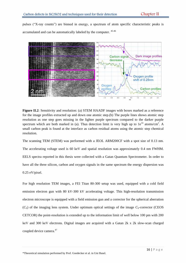
Carbon defects in SiC/SiO2 and techniques used for their detection Chapter II
16 | P a g e *Theoretical simulation performed by Prof. Goedecker et al. in Uni Basel.
pulses (“X-ray counts”) are binned in energy, a spectrum of atom specific characteristic peaks is
accumulated and can be automatically labeled by the computer. 45-46
Figure II.2: Sensitivity and resolution: (a) STEM HAADF images with boxes marked as a reference
for the image profiles extracted up and down one atomic step.(b) The purple lines shows atomic step
resolution as one step goes missing in the lighter purple spectrum compared to the darker purple
spectrum which are both marked in (a). Thus detection limit is very high up to 1e14 atoms/cm2. A
small carbon peak is found at the interface as carbon residual atoms using the atomic step chemical
resolution.
The scanning TEM (STEM) was performed with a JEOL ARM200CF with a spot size of 0.13 nm.
The accelerating voltage used is 60 keV and spatial resolution was approximately 0.4 nm FWHM.
EELS spectra reported in this thesis were collected with a Gatan Quantum Spectrometer. In order to
have all the three silicon, carbon and oxygen signals in the same spectrum the energy dispersion was
0.25 eV/pixel.
For high resolution TEM images, a FEI Titan 80-300 setup was used, equipped with a cold field
emission electron gun with 80 kV-300 kV accelerating voltage. This high-resolution transmission
electron microscope is equipped with a field emission gun and a corrector for the spherical aberration
(CS) of the imaging lens system. Under optimum optical settings of the image CS-corrector (CEOS
CETCOR) the point-resolution is extended up to the information limit of well below 100 pm with 200
keV and 300 keV electrons. Digital images are acquired with a Gatan 2k x 2k slow-scan charged
coupled device camera.47
Carbon defects in SiC/SiO2 and techniques used for their detection Chapter II
17 | P a g e *Theoretical simulation performed by Prof. Goedecker et al. in Uni Basel.
II.3.5 Local Electrode Atom Probe:
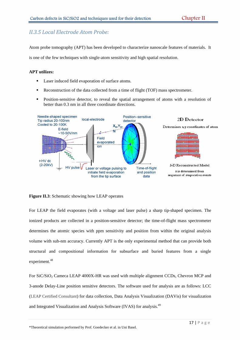
Atom probe tomography (APT) has been developed to characterize nanoscale features of materials. It
is one of the few techniques with single-atom sensitivity and high spatial resolution.
APT utilizes:
Laser induced field evaporation of surface atoms.
Reconstruction of the data collected from a time of flight (TOF) mass spectrometer.
Position-sensitive detector, to reveal the spatial arrangement of atoms with a resolution of
better than 0.3 nm in all three coordinate directions.
Figure II.3: Schematic showing how LEAP operates
For LEAP the field evaporates (with a voltage and laser pulse) a sharp tip-shaped specimen. The
ionized products are collected in a position-sensitive detector; the time-of-flight mass spectrometer
determines the atomic species with ppm sensitivity and position from within the original analysis
volume with sub-nm accuracy. Currently APT is the only experimental method that can provide both
structural and compositional information for subsurface and buried features from a single
experiment.48
For SiC/SiO2 Cameca LEAP 4000X-HR was used with multiple alignment CCDs, Chevron MCP and
3-anode Delay-Line position sensitive detectors. The software used for analysis are as follows: LCC
(LEAP Certified Consultant) for data collection, Data Analysis Visualization (DAVis) for visualization
and Integrated Visualization and Analysis Software (IVAS) for analysis.49
+
40
nm
Carbon defects in SiC/SiO2 and techniques used for their detection Chapter II
18 | P a g e *Theoretical simulation performed by Prof. Goedecker et al. in Uni Basel.
II.3.6 Theoretical Simulation:
Theory: Density functional tight binding methods (DFTB+) give a reliable structure prediction but are
numerically expensive since they require the diagonalization of a Hamiltonian matrix which scales
cubically for large systems.
DFTB explores the potential energy surface in a very efficient way and finds low energy structures.
The minima hopping method has been applied to modify the minimization trajectory and to find the
energy minima structure with higher reliability. Thus, many systems such as clusters, interfaces,
crystalline solids and defects in crystalline solids have been simulated and in many cases entirely new
and unexpected structures have been found. On the Density Functional level the Minima Hopping
method has been applied to some of the largest systems ever studied by unbiased structure prediction
methods with up to 100 atoms. Exploiting the acceleration of the BigDFT electronic structure code
possible with GPU, as well as algorithmic improvements it is even able to do density functional based
structure predictions for systems of several hundred atoms.
The Density-Functional-Theory (DFT) calculations were performed within the projector augmented
wave framework as implemented in the VASP package50 to refine the geometries and energetic
ranking of the most promising candidate structures. We used the generalized gradient approximation
with the Perdew-Burke-Erzernhof (PBE) parametrization of the exchange-correlation functional.51 A
plane-wave cutoff energy of 500 eV was used together with a sufficiently dense k-point mesh,
resulting in total energies converged to less than 1 meV/atom.
II.4 Inference
After being introduced to the instruments required for the identification of defects at interfaces which
can be of few atoms in size, we require very explicit and specific sample preparation as a pre-
condition towards employing such highly proficient equipment. For example thin specimens of 30 nm
thickness are required in the form of wedges or pillars, called ‘TEM-slices’ – for TEM/STEM and

Carbon defects in SiC/SiO2 and techniques used for their detection Chapter II
19 | P a g e *Theoretical simulation performed by Prof. Goedecker et al. in Uni Basel.
LEAP analysis. In the next chapter we will learn about preparation of all the different samples with
their specific geometry necessary for the various measurements.
The MH-DFT is suited to span the whole range from basic to applied research and we will discuss
further in details in the upcoming chapters (theory section).
Chapter III
Sample preparation TGO/pTGO
“By the help of microscopes, there is nothing so small, as to escape our inquiry; hence there
is a new visible world discovered to the understanding.”
Robert Hooke
Summary
Within this chapter the various sample fabrication techniques for the passivated and non-passivated
thermally grown oxides will be explored. Along with the preparation of interface specimen, the
preparation of samples for AFM and Raman Spectroscopy will also be discussed. For TEM/STEM
and LEAP, samples with very specific geometry, interface architecture and thickness are required as
the high resolution images and the analytical results completely depend on these parameters. Hence
sample preparation steps are crucial and play a significant aspect in obtaining meaningful results.
Sample preparation TGO/pTGO Chapter III
21 | P a g e *Theoretical simulation performed by Prof. Goedecker et al. in Uni Basel.
III.1 Introduction
Controlling interface architectures and dopant profiles with minimal defect densities on the nanometer
scale is of eminent importance to advance the efficiency, reliability and device integration efficiency
of semiconductor technologies, in particular to alleviate the current limitations of power
semiconductors and SiC-Metal Oxide Semiconductor Field Effect Transistor (MOSFET) devices. The
first step would be to have a single crystalline SiC wafer and then develop a fabrication process for
defect free gate oxide towards MOSFET.
Growth of single crystalline SiC: It was Lely who obtained single crystalline bulk SiC from
sublimation growth technique in 1955 52. A graphite crucible with SiC powder was heated to 2500 oC
for its sublimation. Governed by a temperature difference, there is a mass transport between outer and
inner part of the crucible of these sublimed species and recrystallization of the single crystalline
platelets occurs. These high quality platelets are then used as a seed for other growth techniques. Later
Tairov and Tsvetkov developed the seeded sublimation growth53 and it is till now the most used
technique. Also, depending on whether it is a Si or a C face nucleate for the bulk growth it will be
either a 6H-SiC or 4H-SiC crystal respectively.54
For device manufacturing the crystal faces of SiC used are the (0001) Si-face, the (0001) C-face or the
(1120) a-face. For the Si-face: it has 100% Si atoms, for the C-face: it has 100% C atoms whereas the
a-face has 50% of each.55 Because of the largely different surface termination layer, the oxidation
rates and interface properties become different for each of the faces.54 For the Si face, SiO2 is
thermally grown on SiC, this is one of the reason for which it is the best successor for silicon
technology as the already developed tools can be directly reassigned and used for its processing.
“Dry” oxidation of SiC for oxide growth happens at 1150 ᴼC, this high temperature is a requirement
in order to grow oxides faster. This is because the oxidation is almost 10 times slower for Si-face in
SiC than on Si (100). Whereas, the oxidation is 5 times slower for the C-face of SiC.
Sample preparation TGO/pTGO Chapter III
22 | P a g e *Theoretical simulation performed by Prof. Goedecker et al. in Uni Basel.
The kinetics of the thermal oxidation of SiC relates to the complex oxidation at the interface which
requires removal of carbon:
2 SiC + 3 O2 → 2 SiO2 + 2 CO (1)
Development of SiC MOSFET: The fabrication of MOSFET includes contacting the source, drain
and gate electrodes. In hindsight there are resemblance between the established Si-based technology
and the SiC technology. The biggest challenge for SiC technology however, is its low channel
mobilities for MOS-devices.
III.2 Scope of Investigation
Although passivating effects have been achieved by post oxidation annealing treatments the
performance of SiC MOSFETs remained limited. To assess the problem a multi-technique approach
for the atomic scale investigation has been chosen. The sample preparation is of utmost importance as
the conclusiveness of the experimental data obtained by different high resolution microscopes and
spectroscopes is completely dependent on the sample preparation including its thickness, height,
position and orientation.
III.3 Sample Preparation
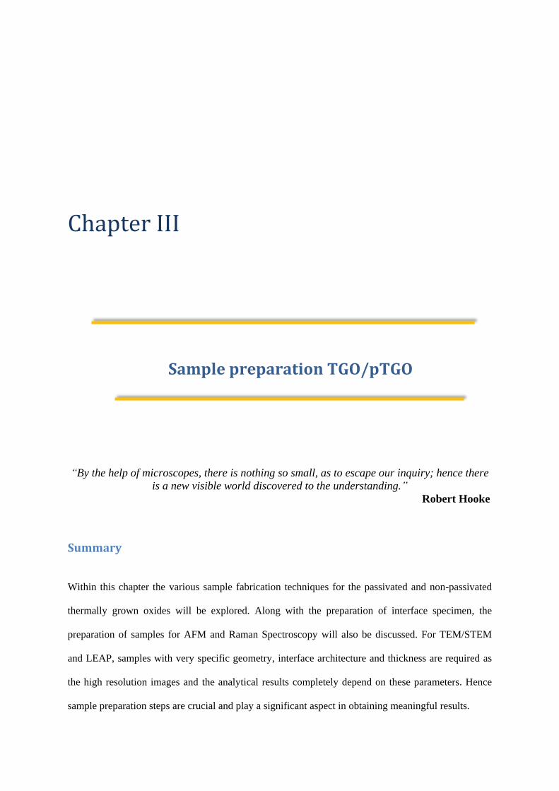
To investigate the near-gate oxide interface region, thermal SiO2/SiC interfaces have been fabricated
within a planar Metal Oxide Semiconductor (MOS) capacitor according to a standard manufacturing
procedure using oxygen at 1150 ᴼC, these samples are referred to as TGO for Thermally Grown
Oxide. As a reference we also investigated pTGO (for Passivated Thermally Grown Oxide) oxidized
in passivating N2O atmosphere. The 50 nm thick SiC/SiO2 epilayers were grown on 4H-SiC wafers
with 4ᴼ off-cut from the same boule by Ascatron, Kista, Sweden. The SiC wafers were exposed to a
pure oxygen atmosphere at 1150 ᴼC for 9 hours for the TGO sample and N2O at 1250 ᴼC for 14 hours
for the pTGO sample. The samples used for all the experiments in this thesis are TGO and pTGO
which are referred in Mikhaylov et al’s work as DRY and TGO respectively.56
Sample preparation TGO/pTGO Chapter III
23 | P a g e *Theoretical simulation performed by Prof. Goedecker et al. in Uni Basel.
Figure III.1. Role of thermal oxidation to fabricate the gate oxide in SiC power devices (a) Schematic
of a basic gate structure with the interface marked as the region of interest. (b) Schematic
representation of the thermal oxidation process for SiC at 1150 ᴼC: In the presence of O2 diffusive
mass transport leads to the progressive oxidation of the carbon in SiC to CO and CO2. This carbon
oxide diffusion via the growing SiO2 layer becomes difficult as the oxidation continues and a thicker
SiO2 layer is formed leading to defects in the interface or gate oxide near channel region reducing the
carrier mobility for the MOSFET device.
III.3.1 Samples for AFM and Raman:
For our experiments the top layer contacts of the fabricated MOS capacitors were stripped off after
their optical and electrical characterization for quality control. This was performed by using a
standard etching solution followed by a subsequent SiO2 removal cycle in 2% HF bath. The duration
of this HF exposure was systematically modified and controlled in order to analyze the effect of the
progressing etch process. The standard etching solution used to remove the oxide contained nitric acid
(HNO3), 7% hydrofluoric acid (HF), and acetic acid CH3COOH) (HF : HNO3 : CH3COOH in
ratio 5 : 1 : 12). The typically used etching time was 2 mins (and 3 mins extra to further remove
nucleates on the TGO sample) for all samples.
We then used room temperature AFM to investigate the MOS capacitor interfaces that have been
prepared by stripping the oxide off as just described, thereby exposing the misoriented 4° off (0001)
Si face of the SiC below the SiC/SiO2 interface.57
For Raman analysis we used samples with and without removing the top layers for both TGO and
pTGO and focused the laser at the concerned region of interest. The absorption of light at 532 nm in
SiC is negligible; hence getting a reasonable signal was possible even after focusing the laser inside
the sample. Consequently, Raman scattering (scattering of a photon by molecules which are excited to
Interfacial Layer with defects
SubstrateOxide
4H-SiCC6, C5, SiOxCySiO2
In: Dry O2 (1150 oC ; 9h) Out: CO+ CO2
Carbon
Oxygen
Silicon
Diffusion
Emission of Co/CO2
Substrate (SiC)
Oxide (SiO2)
Gate (Al metal contact)
Interface SiC/SiO2 (Region of Interest)
(a) (b)
Sample preparation TGO/pTGO Chapter III
24 | P a g e *Theoretical simulation performed by Prof. Goedecker et al. in Uni Basel.
higher energy levels) for a laser focused at the interface provides interface information; whereas the
spectra after setting the laser focus within the bulk SiC will be dominated by the two-phonon bands
from the pure SiC substrate with a negligible interface signal. For SiC the depth of focus is >10 µm58
and our samples were analyzed by moving the focal point from 0 μm to +5 μm.59
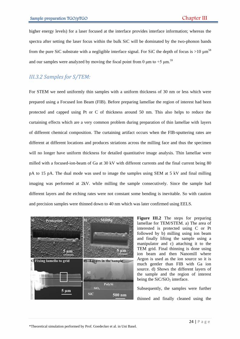
III.3.2 Samples for S/TEM:
For STEM we need uniformly thin samples with a uniform thickness of 30 nm or less which were
prepared using a Focused Ion Beam (FIB). Before preparing lamellae the region of interest had been
protected and capped using Pt or C of thickness around 50 nm. This also helps to reduce the
curtaining effects which are a very common problem during preparation of thin lamellae with layers
of different chemical composition. The curtaining artifact occurs when the FIB-sputtering rates are
different at different locations and produces striations across the milling face and thus the specimen
will no longer have uniform thickness for detailed quantitative image analysis. Thin lamellae were
milled with a focused-ion-beam of Ga at 30 kV with different currents and the final current being 80
pA to 15 pA. The dual mode was used to image the samples using SEM at 5 kV and final milling
imaging was performed at 2kV. while milling the sample consecutively. Since the sample had
different layers and the etching rates were not constant some bending is inevitable. So with caution
and precision samples were thinned down to 40 nm which was later confirmed using EELS.
Figure III.2 The steps for preparing
lamellae for TEM/STEM. a) The area of
interested is protected using C or Pt
followed by b) milling using ion beam
and finally lifting the sample using a
manipulator and c) attaching it to the
TEM grid. Final thinning is done using
ion beam and then Nanomill where
Argon is used as the ion source so it is
much gentler than FIB with Ga ion
source. d) Shows the different layers of
the sample and the region of interest
being the SiC/SiO2 interface.
Subsequently, the samples were further
thinned and finally cleaned using the
5 µm
5 µm5 µm
500 nmSiC
SiO2
PolySi
Al
Protection Milling
Fixing lamella to grid Layers in the sample
a) b)
c) d)
Sample preparation TGO/pTGO Chapter III
25 | P a g e *Theoretical simulation performed by Prof. Goedecker et al. in Uni Basel.
Nanomill system. The lamellae was nanomilled using 900 eV followed by 500 eV for 10 mins each
on both sides of the wedge. The orientation of the lamellae was chosen to be orthogonal to the surface
steps.60
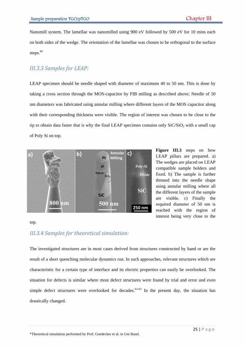
III.3.3 Samples for LEAP:
LEAP specimen should be needle shaped with diameter of maximum 40 to 50 nm. This is done by
taking a cross section through the MOS-capacitor by FIB milling as described above; Needle of 50
nm diameters was fabricated using annular milling where different layers of the MOS capacitor along
with their corresponding thickness were visible. The region of interest was chosen to be close to the
tip to obtain data faster that is why the final LEAP specimen contains only SiC/SiO2 with a small cap
of Poly Si on top.
Figure III.3 steps on how
LEAP pillars are prepared. a)
The wedges are placed on LEAP
compatible sample holders and
fixed. b) The sample is further
thinned into the needle shape
using annular milling where all
the different layers of the sample
are visible. c) Finally the
required diameter of 50 nm is
reached with the region of
interest being very close to the
top.
III.3.4 Samples for theoretical simulation:
The investigated structures are in most cases derived from structures constructed by hand or are the
result of a short quenching molecular dynamics run. In such approaches, relevant structures which are
characteristic for a certain type of interface and its electric properties can easily be overlooked. The
situation for defects is similar where most defect structures were found by trial and error and even
simple defect structures were overlooked for decades.61-63 In the present day, the situation has
drastically changed.
250 nm
SiC
Poly-Si
Oxide
800 nm
Pt
Poly-Si
SiC
Annular Milling
Si O2
500 nm
a) b) c)

Sample preparation TGO/pTGO Chapter III
26 | P a g e *Theoretical simulation performed by Prof. Goedecker et al. in Uni Basel.
Minima hopping method (MHM)61, 64-65 simulations were performed using the MINHOCAO package
based on the DFTB66-68 scheme to evaluate the potential energy landscape. The MHM is a highly
efficient algorithm to identify the ground state structure of any condensed matter system by sampling
the energy landscape, based solely on the information of the chemical composition. Short molecular
dynamics escape steps are performed to overcome energy barriers while exploiting the Bell-Evans-
Polanyi principle in order to accelerate the search69 followed by local geometry optimizations. The
structural searches were conducted with surface slabs with supercell sizes of 1x1 and 4x4, scanning
several hundred different structures. Initial SiC/SiO2 structures were randomly allowed to generate in
an unbiased way. The surface model was constructed with a 10Å vacuum gap perpendicular to the
surface. The atomic structures were relaxed until the forces on the atoms were less than 3 meV/ Å and
the stresses were less than 0.1 eV/ Å. The normal modes were calculated using the DFTB scheme.
III.4 Inference
The sample preparation is time consuming and very difficult because of the different layers with
different etching rates. Hence maintaining a uniform sample thickness and avoiding bending for the
layered specimen is complex. After learning about the various sample preparation techniques we shall
now concentrate on how to investigate them near our region of interest.
Chapter IV
Atomistic analysis of SiC/SiO2 Interface to find C-
defects
“A picture is worth a thousand words. An interface is worth a thousand pictures.”
Ben Shneiderman
Summary
The key to the mobility enhancements is the identification of the defects along with their origin and
discovery of further new or improved passivation methods to conciliate the interfacial defects. In this
chapter we present thorough investigations and unique concerting evidence supporting the presence of
interface defects in the form of carbon nucleates, due to the complex thermal oxidation of SiC during
the gate oxide fabrication.
Atomistic analysis of SiC/SiO2 Interface to find C-defects Chapter IV
28 | P a g e *Theoretical simulation performed by Prof. Goedecker et al. in Uni Basel.
IV.1 Introduction
In SiC MOSFETs, the inversion channel significantly contributes to the total on-resistance. The
quality of the interface is thus crucial for device performance as it highly affects the channel mobility.
The density of interface states at the SiO2/SiC interface is at least two to three orders of magnitude
higher (~1012 eV−1 cm−2) compared to the relatively matured Si/SiO2 interface.21
As reviewed in chapter I and II the quality of the interface is directly reflected in the channel mobility
of MOSFETs. Carriers when injected in the ON and the OFF state it may get trapped at the SiC/oxide
interface defect states and cause Coulomb scattering. The trap density is critical as it determines the
device stability and also reliability. As discussed in chapter II carbon is found to be one of the stable
defects at the interface which can be present in a variety of configurations. For example, if we
consider a Si-O-Si bridge: the single carbon atom can interfere and form Si-C-Si bond with another
oxygen or can form Si-O-C-Si bond linked to a Si atom on a neighboring ring. These defects can be
stable in either the neutral state or the negatively charged states. This yields to a “C-cluster” also
called “C-nucleate” of around 6 atoms. Such defect have been debated over for decades and plays an
imperative role towards improving future SiC MOSFETs.
In this chapter both theoretical and experimental approaches to investigate the atomistic and electronic
structure of the SiC/SiO2 interface have been discussed in order to draw conclusions in view of SiC
device technology.
IV.2 Scope of Investigation
As discussed in the previous chapters excess carbon atoms can aggregate to form graphitic clusters at
the SiO2/SiC interface and they can be of different sizes. Depending on the cluster size and the atomic
environment the π orbital of these sp2-bonded carbon can give rise to different energy levels. For
example small C-clusters should give rise to energy levels near the lower part of the band gap whereas
large clusters would have graphite-like energy levels in the gap. There can also be a third C-related
Atomistic analysis of SiC/SiO2 Interface to find C-defects Chapter IV
29 | P a g e *Theoretical simulation performed by Prof. Goedecker et al. in Uni Basel.
energy level near the upper region of the band gap due to 3C-SiC inclusions at the SiO2/4H-SiC
surface.70-71
The current scientific literature on the presence or absence of certain defects is overall inconclusive
and partially contradictory. There are reports concluding that carbon clusters may be present while
others conclude that near interface carbon clusters are just myths and that it is the interface roughness
which plays a vital role in reducing the mobility in SiC device. Hence both theoretical and
experimental investigations are of immense priority for finding the carbon defects.
IV.3 Results and Discussion
For both samples TGO and pTGO, we observe terraces and step bunch areas on SiC in the AFM
images, which can be attributed to regions (steps/terraces) with different surface/interface energies.72-
73 The quasi-periodic step like structure is interesting as it looks similar to the surface morphology
after step-flow74 like growth processes,75-76 but occurs here below the surface, at the oxide/SiC
interface. Analysis of the AFM data reveals that the step-bunched areas vary in height.77-78 Single step
heights are in the order of ~0.75 nm while the larger step bunched areas exhibit a step height of ~1.5
to 3.5 nm, close to the size of one 4H-SiC unit cell (4 bilayers along the 001 direction).
(The work in section IV.3.1 to IV.3.3 is submitted to APL)
IV.3.1 Visualizing the C-defects at the interface:
The most striking characteristics of the AFM micrograph of the oxide stripped TGO interfaces are the
clearly observable nucleates (size ~2 to ~6 nm) arranged like arrays of pearl necklaces. These are
small particles, nucleates, which are especially apparent in the AFM images after the first oxide
removal and cleaning cycle (2 mins, 2% HF) (Figure IV.1a) and are frequently, but not exclusively,
located on the bunched step areas. After a second cycle of HF cleaning for another 2 mins, the number
of these nucleates declines drastically (Figure IV.1b). In contrast to the TGO samples, the wafers
oxidized in N2O i.e., pTGO show a clean surface morphology with virtually no etch resistant
nucleates present on the interface after oxide stripping (see Figure IV.1c). It is well known that

Atomistic analysis of SiC/SiO2 Interface to find C-defects Chapter IV
30 | P a g e *Theoretical simulation performed by Prof. Goedecker et al. in Uni Basel.
oxidation in a passivating atmosphere like N2O produces interfaces with less electronically active
defects.79 It is, thus, plausible to see significantly less nucleates at interfaces prepared by oxidation in
the N2O passivating agent. This may explain the poorer MOS performance of gate oxide interfaces
grown in pure oxygen atmosphere (TGO) compared to the significantly improved, but still
dissatisfactory, performance of the N2O passivated samples (pTGO). The poor performance of the SiC
MOS in comparison to Si is thus attributed to the presence of Carbon in the oxidation procedure. The
oxidized carbon is expected to diffuse to the surface through the growing SiO2 layer and to be
released as CO/CO2 into the process gas. The continuous diffusion of C and O during the thermal
oxidation process will modify the solid matrix and leaves defects behind that broaden the interface
and affect the structural integrity of the SiO2 and the near-interface region of the SiC.26 The nucleates
present at SiC/SiO2 interfaces resisted HF etching but could be removed by Ozone. We attribute the
behavior to the fact that the nucleates are carbon clusters, an observation in our own findings (chapter
V) in agreement with an earlier report.40, 80 The strong dependence of the observed nucleate density on
the oxidation process rules out that the nucleates originate from imperfections in the SiC wafer, since
the wafers are from the same batch.
In order to provide a better microscopic understanding of the defects occurring during the thermal
oxidation of SiC, we have performed atomistic simulations based on advanced structural sampling
algorithms. We employ the Minima hopping (MH) structure prediction method 61, 69 together with the
Density Functional Tight Binding (DFTB) scheme66-68 to explore the complex energy landscape
during the oxidation process. To this end, we use two different chemical configurations to model two
distinct conditions during the oxidation process. In model A, we provide a larger amount of oxygen
(more than the oxygen required to convert the topmost layer into a stoichiometric SiO2 pattern) at the
interface than required to oxidize the first surface layer, which corresponds to a one-step oxidation
process. In model B, we create an oxygen deficient reaction environment to mimic a two-step
oxidation process. Thereby, the surface is first oxidized with half of the oxygen required to convert
the topmost layer into a stoichiometric SiO2 pattern before more oxygen is added.
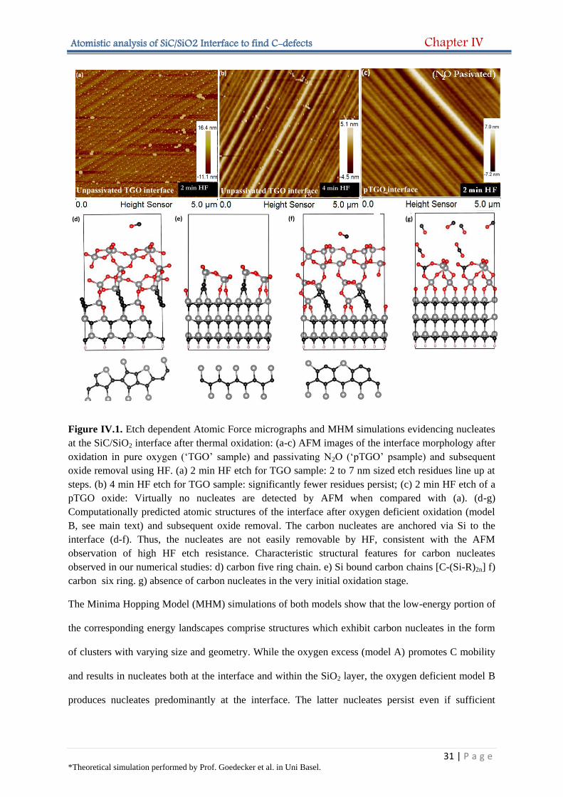
Atomistic analysis of SiC/SiO2 Interface to find C-defects Chapter IV
31 | P a g e *Theoretical simulation performed by Prof. Goedecker et al. in Uni Basel.
Figure IV.1. Etch dependent Atomic Force micrographs and MHM simulations evidencing nucleates
at the SiC/SiO2 interface after thermal oxidation: (a-c) AFM images of the interface morphology after
oxidation in pure oxygen (‘TGO’ sample) and passivating N2O (‘pTGO’ psample) and subsequent
oxide removal using HF. (a) 2 min HF etch for TGO sample: 2 to 7 nm sized etch residues line up at
steps. (b) 4 min HF etch for TGO sample: significantly fewer residues persist; (c) 2 min HF etch of a
pTGO oxide: Virtually no nucleates are detected by AFM when compared with (a). (d-g)
Computationally predicted atomic structures of the interface after oxygen deficient oxidation (model
B, see main text) and subsequent oxide removal. The carbon nucleates are anchored via Si to the
interface (d-f). Thus, the nucleates are not easily removable by HF, consistent with the AFM
observation of high HF etch resistance. Characteristic structural features for carbon nucleates
observed in our numerical studies: d) carbon five ring chain. e) Si bound carbon chains [C-(Si-R)2n] f)
carbon six ring. g) absence of carbon nucleates in the very initial oxidation stage.
The Minima Hopping Model (MHM) simulations of both models show that the low-energy portion of
the corresponding energy landscapes comprise structures which exhibit carbon nucleates in the form
of clusters with varying size and geometry. While the oxygen excess (model A) promotes C mobility
and results in nucleates both at the interface and within the SiO2 layer, the oxygen deficient model B
produces nucleates predominantly at the interface. The latter nucleates persist even if sufficient
2 min HF 4 min HF
(a) (b)
(d) (e) (f) (g)
Unpassivated TGO interface Unpassivated TGO interface pTGO interface
2
Atomistic analysis of SiC/SiO2 Interface to find C-defects Chapter IV
32 | P a g e *Theoretical simulation performed by Prof. Goedecker et al. in Uni Basel.
oxygen is provided in a second step. The structural features of the carbon nucleates are similar in
both models, and consist of characteristic five (C5) and six (C6) membered rings. In presence of
sufficient oxygen (model A), these carbon rings form covalent bonds to the surrounding Si atoms in
the SiC and/ or SiO2 matrix (Fig. 2d). On the other hand, the oxygen-deficient model B leads initially
to chain-like carbon structures, which subsequently convert in a second step to interlinked chains of
carbon rings as the MHM simulation progresses (chains of C5 (Figure IV.1d) or of C6-rings (Figure
IV.1f), and zig-zag carbon chains [C-(Si-R)2]n (Figure IV.1e)). These chain structures exhibit an
especially high energetic stability at specific interface sites: the periodic silicon carbide matrix
anchors/passivates the chains and ribbons from the bottom, while the Si atoms from the SiO2 layer
bond from the top. Occasionally the simulation finds cases where the carbon atoms contained in the
unit box do not nucleate (Figure IV.1g), but form merely CO and CO2 as the oxidation products.
The simulated C5 and C6 clusters readily represent the initial stages of the nucleation and growth
process resulting in the HF etch resistant nucleates with a certain carbon content.81 Figure IV.1d-g
shows how the nucleates form in the initial state of the oxygen deficient oxidation (model B). The C
nucleates are attached to the SiC matrix in agreement with the AFM results. Figure IV.2c-h shows the
C nucleates formed after further oxygen was provided in the second step (model B). In this case the
nucleates are not only present at the interface but move into the SiO2 as well. In our AFM data we
observed the etch resistant carbon to preferably nucleate at or near SiC steps, thereby extending the
pre-existing nucleates into larger structures while maintaining contact to the growth front of the
interface as it moves deeper into the SiC wafer. Thus, the observed 2-5 nm sized nucleates emerge
from the thermal oxidation as it progresses into the wafer. The pearl necklace morphology indicates
that certain interface features, e.g., step bunched areas may also play a role.
IV.3.2 Chemical analysis for unwanted C-bonds at interface:
A conclusive determination of the structure and composition of these nucleates is not possible based
solely on the previous results. Hence, we use second order Raman spectroscopy to analyze the binding
of the different carbon species in the near interface region. Depending on the focus setting and on the
Atomistic analysis of SiC/SiO2 Interface to find C-defects Chapter IV
33 | P a g e *Theoretical simulation performed by Prof. Goedecker et al. in Uni Basel.
focus position with respect to the interface, this technique allows us to distinguish different regions
below and above the interface within micrometer scale resolution. The Raman spectra contain the
integral signals from the structures present within the interaction volume of the focus spot. Our
system’s spot volume is at most 2 µm wide and 3 µm deep and we focused at the interface and +5 µm
into the bulk. The signal at the +5 µm focus position i.e. with the focus set within the bulk SiC sample
contains insignificant, below noise level, contributions from surface/interface scattering. The bulk
signal is of high intensity as the penetration depth of the laser light at 532 nm wavelength into SiC is
large. Each spectrum was recorded for 2 min and integrated over 15 measurements. The systematic
change of the shape of Raman spectra with changing position of the stage and focus position is clearly
shown in Figure IV.2a. The samples used were the same TGO and pTGO after the oxide was removed
from the top. To facilitate the identification of the carbon bonds at the interface of SiC, we subtract
the background/ reference spectra from the TGO spectra. Two background/ reference spectra have
been used for more statistical confirmation: as discussed in detail in Figure IV.2a. The resulting
Raman spectrum after the background correction with a clean SiC wafer shown in Figure IV.2b,
exhibits ten sharp peaks corresponding to vibrational excitation modes of bonds associated with the
different carbon species in different bonding states (Table 1).58 We identified 10 distinct peaks in the
background subtracted Raman data and after comparing them to literature values we found each of
them to corresponded to a C-peak which is different from the sp3 carbon in SiC and which should not
be present at the interface or inside SiC/SiO2.58
We compared our results with the report by Borowicz et al.58 to find that Finite size carbon crystals
and/or benzene-like rings are associated with the Raman peak at 1477 cm-1. The Full Width at Half
Maximum (FWHM) we observe here, however, is broader than observed in typical such bands.82-84
This broadening might be associated to the very small size of the C-defects in our samples. The main
Raman signals associated with carbon bonds in graphite are the D (defective) and G (graphitic) bands
characterized by the highest intensity at 1350 cm-1 and 1580 cm-1, respectively.85 Importantly, there is
the possibility for the G band to shift depending on the C=C vibrations to higher frequencies of about
1620 cm-1.86 The graphitic carbon is recognized by the graphitic band or G-band @ 1622 cm-1,
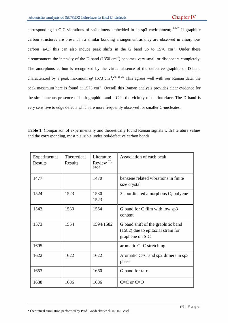
Atomistic analysis of SiC/SiO2 Interface to find C-defects Chapter IV
34 | P a g e *Theoretical simulation performed by Prof. Goedecker et al. in Uni Basel.
corresponding to C-C vibrations of sp2 dimers embedded in an sp3 environment; 85-87 If graphitic
carbon structures are present in a similar bonding arrangement as they are observed in amorphous
carbon (a-C) this can also induce peak shifts in the G band up to 1570 cm-1. Under these
circumstances the intensity of the D band (1350 cm-1) becomes very small or disappears completely.
The amorphous carbon is recognized by the virtual absence of the defective graphite or D-band
characterized by a peak maximum @ 1573 cm-1.20, 28-30 This agrees well with our Raman data: the
peak maximum here is found at 1573 cm-1. Overall this Raman analysis provides clear evidence for
the simultaneous presence of both graphitic and a-C in the vicinity of the interface. The D band is
very sensitive to edge defects which are more frequently observed for smaller C-nucleates.
Table 1: Comparison of experimentally and theoretically found Raman signals with literature values
and the corresponding, most plausible undesired/defective carbon bonds
Experimental
Results
Theoretical
Results
Literature
Review 20,
28-30
Association of each peak
1477 1470 benzene related vibrations in finite
size crystal
1524 1523 1530
1523
3 coordinated amorphous C; polyene
1543 1530 1554 G band for C film with low sp3
content
1573 1554 1594/1582 G band shift of the graphitic band
(1582) due to epitaxial strain for
graphene on SiC
1605 aromatic C=C stretching
1622 1622 1622 Aromatic C=C and sp2 dimers in sp3
phase
1653 1660 G band for ta-c
1688 1686 1686 C=C or C=O
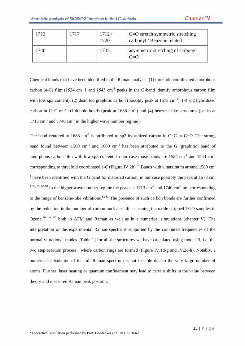
Atomistic analysis of SiC/SiO2 Interface to find C-defects Chapter IV
35 | P a g e *Theoretical simulation performed by Prof. Goedecker et al. in Uni Basel.
1713 1717 1712 /
1720
C=O stretch symmetric stretching
carbonyl / Benzene related
1740 1735
asymmetric stretching of carbonyl
C=O
Chemical bonds that have been identified in the Raman analysis: (1) threefold coordinated amorphous
carbon (a-C) film (1524 cm−1 and 1543 cm-1 peaks in the G-band identify amorphous carbon film
with low sp3 content), (2) distorted graphitic carbon (possibly peak at 1573 cm-1), (3) sp2 hybridized
carbon in C=C or C=O double bonds (peak at 1688 cm-1) and (4) benzene like structures (peaks at
1713 cm-1 and 1740 cm-1 in the higher wave number regime).
The band centered at 1688 cm-1 is attributed to sp2 hybridized carbon in C=C or C=O. The strong
band found between 1500 cm-1 and 1600 cm-1 has been attributed to the G (graphitic) band of
amorphous carbon film with low sp3 content. In our case those bands are 1524 cm-1 and 1543 cm-1
corresponding to threefold coordinated a-C (Figure IV.2b).84 Bands with a maximum around 1580 cm-
1 have been identified with the G band for distorted carbon, in our case possibly the peak at 1573 cm-
1.58, 85, 87-88 In the higher wave number regime the peaks at 1713 cm-1 and 1740 cm-1 are corresponding
to the range of benzene-like vibrations.82-83 The presence of such carbon bonds are further confirmed
by the reduction in the number of carbon nucleates after cleaning the oxide stripped TGO samples in
Ozone;20, 40, 80 both in AFM and Raman as well as in a numerical simulations (chapter V). The
interpretation of the experimental Raman spectra is supported by the computed frequencies of the
normal vibrational modes [Table 1] for all the structures we have calculated using model B, i.e. the
two step reaction process, where carbon rings are formed (Figure IV.1d-g and IV.2c-h). Notably, a
numerical calculation of the full Raman spectrum is not feasible due to the very large number of
atoms. Further, laser heating or quantum confinement may lead to certain shifts in the value between
theory and measured Raman peak position.
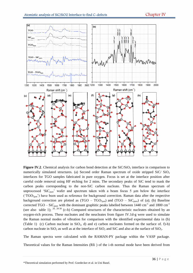
Atomistic analysis of SiC/SiO2 Interface to find C-defects Chapter IV
36 | P a g e *Theoretical simulation performed by Prof. Goedecker et al. in Uni Basel.
Figure IV.2. Chemical analysis for carbon bond detection at the SiC/SiO2 interface in comparison to
numerically simulated structures. (a) Second order Raman spectrum of oxide stripped SiC/ SiO2
interfaces for TGO samples fabricated in pure oxygen. Focus is set at the interface position after
careful oxide removal using HF etching for 2 mins. The secondary peaks of SiC tend to mask the
carbon peaks corresponding to the non-SiC carbon nucleate. Thus the Raman spectrum of
unprocessed ‘SiCpure’ wafer and spectrum taken with a beam focus 5 µm below the interface
(‘TGO5µm’) have been used as reference for background correction. Raman data after the respective
background correction are plotted as (TGO – TGO5μm) and (TGO – SiCpure) of (a); (b) Baseline
corrected TGO – SiCpure with the dominant graphitic peaks labelled between 1440 cm-1 and 1800 cm-1
(see also table 1); 20, 28-30 (c-h) Computed structures of the characteristic nucleates obtained by an
oxygen-rich process. These nucleates and the neucleates from figure IV.1d-g were used to simulate
the Raman normal modes of vibration for comparison with the identified experimental data in (b)
(Table 1) (c) Carbon nucleate in SiO2, d) and e) carbon nucleates formed on the surface of. f)-h)
carbon nucleate in SiO2 as well as at the interface of SiO2 and SiC and also at the surface of SiO2.
The Raman spectra were calculated with the RAMAN-PY package within the VASP package.
Theoretical values for the Raman Intensities (RIi ) of the i-th normal mode have been derived from
(a)(b)
(c) (d) (e) (f) (g) (h)
TGO – TGO5μm
TGO
TGO5μm
TGO – SiCpure
SiCpure
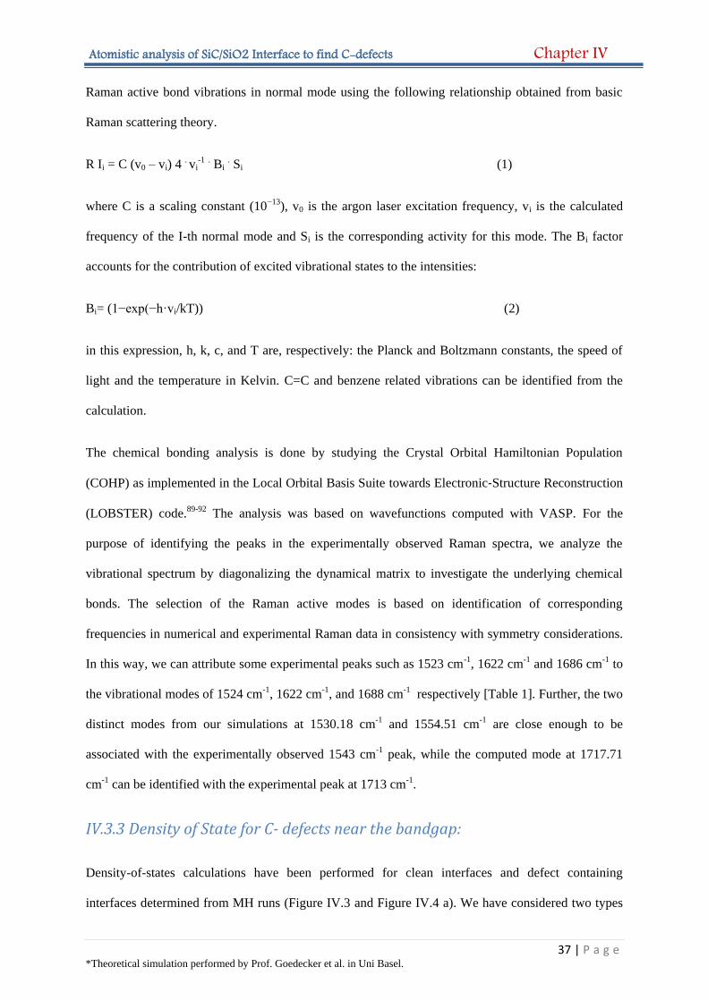
Atomistic analysis of SiC/SiO2 Interface to find C-defects Chapter IV
37 | P a g e *Theoretical simulation performed by Prof. Goedecker et al. in Uni Basel.
Raman active bond vibrations in normal mode using the following relationship obtained from basic
Raman scattering theory.
R Ii = C (v0 – vi) 4 . vi-1 . Bi
. Si (1)
where C is a scaling constant (10−13), v0 is the argon laser excitation frequency, vi is the calculated
frequency of the I-th normal mode and Si is the corresponding activity for this mode. The Bi factor
accounts for the contribution of excited vibrational states to the intensities:
Bi= (1−exp(−h·vi/kT)) (2)
in this expression, h, k, c, and T are, respectively: the Planck and Boltzmann constants, the speed of
light and the temperature in Kelvin. C=C and benzene related vibrations can be identified from the
calculation.
The chemical bonding analysis is done by studying the Crystal Orbital Hamiltonian Population
(COHP) as implemented in the Local Orbital Basis Suite towards Electronic‐Structure Reconstruction
(LOBSTER) code.89-92 The analysis was based on wavefunctions computed with VASP. For the
purpose of identifying the peaks in the experimentally observed Raman spectra, we analyze the
vibrational spectrum by diagonalizing the dynamical matrix to investigate the underlying chemical
bonds. The selection of the Raman active modes is based on identification of corresponding
frequencies in numerical and experimental Raman data in consistency with symmetry considerations.
In this way, we can attribute some experimental peaks such as 1523 cm-1, 1622 cm-1 and 1686 cm-1 to
the vibrational modes of 1524 cm-1, 1622 cm-1, and 1688 cm-1 respectively [Table 1]. Further, the two
distinct modes from our simulations at 1530.18 cm-1 and 1554.51 cm-1 are close enough to be
associated with the experimentally observed 1543 cm-1 peak, while the computed mode at 1717.71
cm-1 can be identified with the experimental peak at 1713 cm-1.
IV.3.3 Density of State for C- defects near the bandgap:
Density-of-states calculations have been performed for clean interfaces and defect containing
interfaces determined from MH runs (Figure IV.3 and Figure IV.4 a). We have considered two types
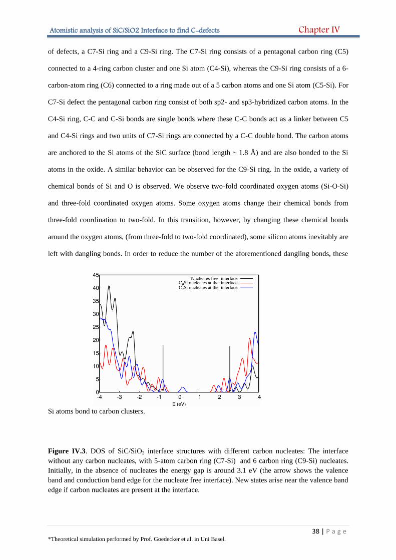
Atomistic analysis of SiC/SiO2 Interface to find C-defects Chapter IV
38 | P a g e *Theoretical simulation performed by Prof. Goedecker et al. in Uni Basel.
of defects, a C7-Si ring and a C9-Si ring. The C7-Si ring consists of a pentagonal carbon ring (C5)
connected to a 4-ring carbon cluster and one Si atom (C4-Si), whereas the C9-Si ring consists of a 6-
carbon-atom ring (C6) connected to a ring made out of a 5 carbon atoms and one Si atom (C5-Si). For
C7-Si defect the pentagonal carbon ring consist of both sp2- and sp3-hybridized carbon atoms. In the
C4-Si ring, C-C and C-Si bonds are single bonds where these C-C bonds act as a linker between C5
and C4-Si rings and two units of C7-Si rings are connected by a C-C double bond. The carbon atoms
are anchored to the Si atoms of the SiC surface (bond length ~ 1.8 Å) and are also bonded to the Si
atoms in the oxide. A similar behavior can be observed for the C9-Si ring. In the oxide, a variety of
chemical bonds of Si and O is observed. We observe two-fold coordinated oxygen atoms (Si-O-Si)
and three-fold coordinated oxygen atoms. Some oxygen atoms change their chemical bonds from
three-fold coordination to two-fold. In this transition, however, by changing these chemical bonds
around the oxygen atoms, (from three-fold to two-fold coordinated), some silicon atoms inevitably are
left with dangling bonds. In order to reduce the number of the aforementioned dangling bonds, these
Si atoms bond to carbon clusters.
Figure IV.3. DOS of SiC/SiO2 interface structures with different carbon nucleates: The interface
without any carbon nucleates, with 5-atom carbon ring (C7-Si) and 6 carbon ring (C9-Si) nucleates.
Initially, in the absence of nucleates the energy gap is around 3.1 eV (the arrow shows the valence
band and conduction band edge for the nucleate free interface). New states arise near the valence band
edge if carbon nucleates are present at the interface.
Atomistic analysis of SiC/SiO2 Interface to find C-defects Chapter IV
39 | P a g e *Theoretical simulation performed by Prof. Goedecker et al. in Uni Basel.
Finally, we use Density Functional Theory (DFT) calculations to analyze the electronic band structure
of the SiC/SiO2 interface based on our atomistic model. Most of the previously reported Density of
States (DOS) calculations were performed for small carbon cluster doped SiC or linear carbon clusters
at the SiC/SiO2 interface.50, 93-96 We compute the DOS for the structural models in Figure IV.3 which
consist of C-Si rings as defect states and compare them to the DOS of pristine SiC. Figure IV.3 shows
that defect states emerge in the band gap of the pristine semiconductor. An atom projected DOS is
shown in Figure IV.4, which clearly associates these defect levels to the p-states of the carbon
nucleates in the vicinity of the interface. These results support the assumption that the carbon
nucleates cause low mobility at the interface due to electronic states in the band gap which are
responsible for the deterioration of the interface-near electronic properties.
The band gap calculated for SiC/SiO2 interfaces depends on the methods used. It is 2.84 eV using the
Perdew–Burke-Ernzerhof (PBE) potential; with different hybrid potentials such as PBE0 the band gap
is calculated to be 4.1 eV and by using the Heyd-Scuseria-Ernzerhof (HSE) potential it is 3.4 eV. The
band gap determined by HSE is significantly closer to the experimental value.30 Hence all electronic
properties were calculated using the HSE06 hybrid functional with the kpoints of 6X6X1. We find
that the bandgap of structures which contain carbon nucleates is reduced. There are new states formed
near the valence band and some mid-gap states are also observed depending on the nucleate shape.
For 5-ring C nucleates (C7-Si in Figure. IV.3 and Figure. IV.4), the valence band edge is shifted up
and the conduction band edge is shifted down significantly reducing the band gap to 2.3 eV. In
addition a very stable defect state occupying the mid-gap state appears at -0.5 eV above the shifted
valence band edge. The most important contribution for these new states comes from overlapping px
states between the neighboring carbon atoms in the nucleates. A smaller contribution originates from
py and pz states. The occupied levels appear due to the p-p interaction between the nearest neighbor
carbon atoms in the carbon nucleate.
For 6-ring carbon nucleates (C9-Si in Figure. IV.3 and IV.4) at the interface, the valence band is
shifted upwards by 0.5 eV and the conduction band edge is shifted downward by 1.3 eV. The carbon
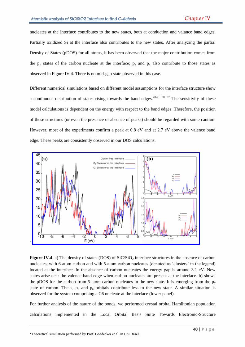
Atomistic analysis of SiC/SiO2 Interface to find C-defects Chapter IV
40 | P a g e *Theoretical simulation performed by Prof. Goedecker et al. in Uni Basel.
nucleates at the interface contributes to the new states, both at conduction and valance band edges.
Partially oxidized Si at the interface also contributes to the new states. After analyzing the partial
Density of States (pDOS) for all atoms, it has been observed that the major contribution comes from
the py states of the carbon nucleate at the interface; pz and px also contribute to those states as
observed in Figure IV.4. There is no mid-gap state observed in this case.
Different numerical simulations based on different model assumptions for the interface structure show
a continuous distribution of states rising towards the band edges.20-21, 30, 97 The sensitivity of these
model calculations is dependent on the energy with respect to the band edges. Therefore, the position
of these structures (or even the presence or absence of peaks) should be regarded with some caution.
However, most of the experiments confirm a peak at 0.8 eV and at 2.7 eV above the valence band
edge. These peaks are consistently observed in our DOS calculations.
`
Figure IV.4. a) The density of states (DOS) of SiC/SiO2 interface structures in the absence of carbon
nucleates, with 6-atom carbon and with 5-atom carbon nucleates (denoted as ‘clusters’ in the legend)
located at the interface. In the absence of carbon nucleates the energy gap is around 3.1 eV. New
states arise near the valence band edge when carbon nucleates are present at the interface. b) shows
the pDOS for the carbon from 5-atom carbon nucleates in the new state. It is emerging from the py
state of carbon. The s, px and pz orbitals contribute less to the new state. A similar situation is
observed for the system comprising a C6 nucleate at the interface (lower panel).
For further analysis of the nature of the bonds, we performed crystal orbital Hamiltonian population
calculations implemented in the Local Orbital Basis Suite Towards Electronic‐Structure
(a) (b)
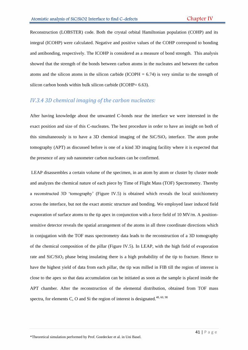
Atomistic analysis of SiC/SiO2 Interface to find C-defects Chapter IV
41 | P a g e *Theoretical simulation performed by Prof. Goedecker et al. in Uni Basel.
Reconstruction (LOBSTER) code. Both the crystal orbital Hamiltonian population (COHP) and its
integral (ICOHP) were calculated. Negative and positive values of the COHP correspond to bonding
and antibonding, respectively. The ICOHP is considered as a measure of bond strength. This analysis
showed that the strength of the bonds between carbon atoms in the nucleates and between the carbon
atoms and the silicon atoms in the silicon carbide (ICOPH = 6.74) is very similar to the strength of
silicon carbon bonds within bulk silicon carbide (ICOHP= 6.63).
IV.3.4 3D chemical imaging of the carbon nucleates:
After having knowledge about the unwanted C-bonds near the interface we were interested in the
exact position and size of this C-nucleates. The best procedure in order to have an insight on both of
this simultaneously is to have a 3D chemical imaging of the SiC/SiO2 interface. The atom probe
tomography (APT) as discussed before is one of a kind 3D imaging facility where it is expected that
the presence of any sub nanometer carbon nucleates can be confirmed.
LEAP disassembles a certain volume of the specimen, in an atom by atom or cluster by cluster mode
and analyzes the chemical nature of each piece by Time of Flight Mass (TOF) Spectrometry. Thereby
a reconstructed 3D ‘tomography’ (Figure IV.5) is obtained which reveals the local stoichiometry
across the interface, but not the exact atomic structure and bonding. We employed laser induced field
evaporation of surface atoms to the tip apex in conjunction with a force field of 10 MV/m. A position-
sensitive detector reveals the spatial arrangement of the atoms in all three coordinate directions which
in conjugation with the TOF mass spectrometry data leads to the reconstruction of a 3D tomography
of the chemical composition of the pillar (Figure IV.5). In LEAP, with the high field of evaporation
rate and SiC/SiO2 phase being insulating there is a high probability of the tip to fracture. Hence to
have the highest yield of data from each pillar, the tip was milled in FIB till the region of interest is
close to the apex so that data accumulation can be initiated as soon as the sample is placed inside the
APT chamber. After the reconstruction of the elemental distribution, obtained from TOF mass
spectra, for elements C, O and Si the region of interest is designated.48, 60, 98
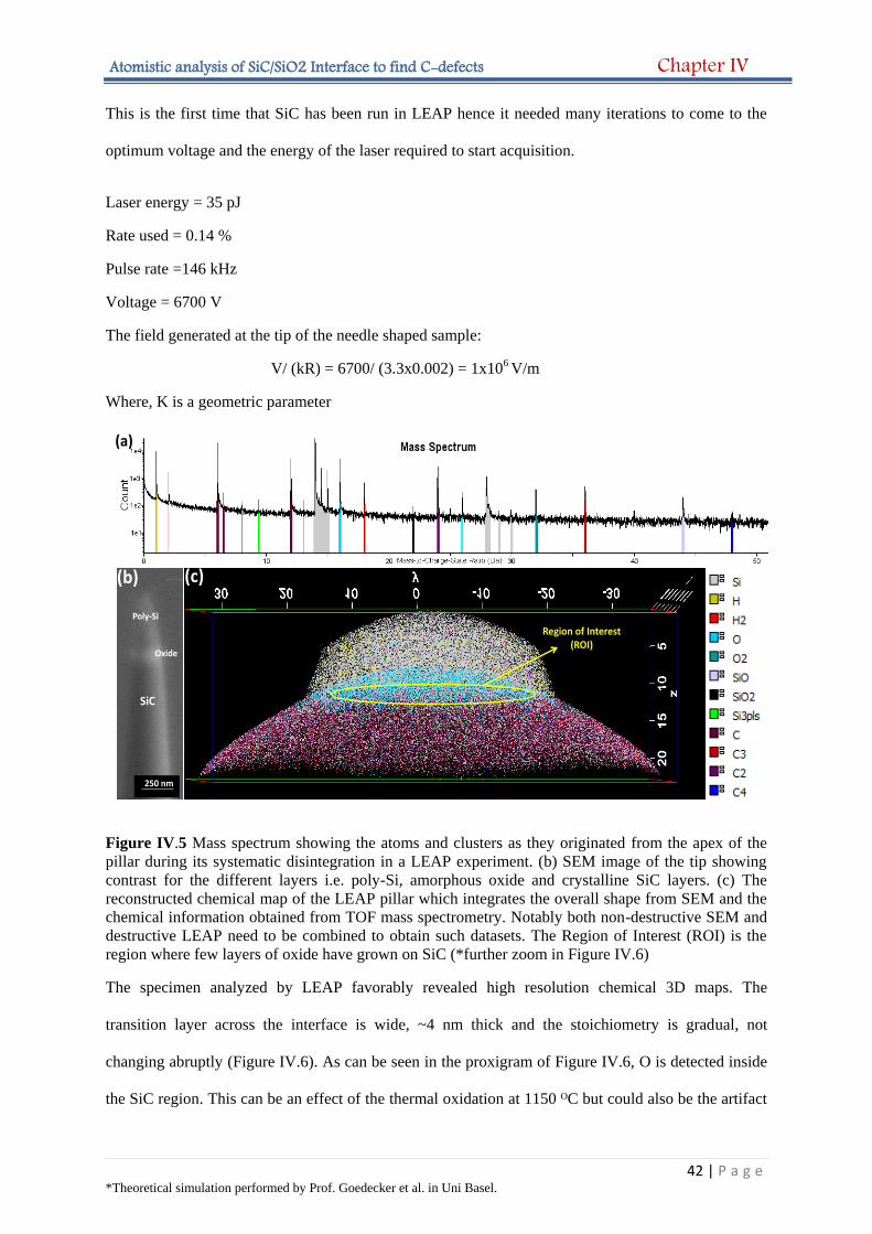
Atomistic analysis of SiC/SiO2 Interface to find C-defects Chapter IV
42 | P a g e *Theoretical simulation performed by Prof. Goedecker et al. in Uni Basel.
This is the first time that SiC has been run in LEAP hence it needed many iterations to come to the
optimum voltage and the energy of the laser required to start acquisition.
Laser energy = 35 pJ
Rate used = 0.14 %
Pulse rate =146 kHz
Voltage = 6700 V
The field generated at the tip of the needle shaped sample:
V/ (kR) = 6700/ (3.3x0.002) = 1x10⁶ V/m
Where, K is a geometric parameter
Figure IV.5 Mass spectrum showing the atoms and clusters as they originated from the apex of the
pillar during its systematic disintegration in a LEAP experiment. (b) SEM image of the tip showing
contrast for the different layers i.e. poly-Si, amorphous oxide and crystalline SiC layers. (c) The
reconstructed chemical map of the LEAP pillar which integrates the overall shape from SEM and the
chemical information obtained from TOF mass spectrometry. Notably both non-destructive SEM and
destructive LEAP need to be combined to obtain such datasets. The Region of Interest (ROI) is the
region where few layers of oxide have grown on SiC (*further zoom in Figure IV.6)
The specimen analyzed by LEAP favorably revealed high resolution chemical 3D maps. The
transition layer across the interface is wide, ~4 nm thick and the stoichiometry is gradual, not
changing abruptly (Figure IV.6). As can be seen in the proxigram of Figure IV.6, O is detected inside
the SiC region. This can be an effect of the thermal oxidation at 1150 ᴼC but could also be the artifact
250 nm
SiC
Poly-Si
Oxide
Region of Interest(ROI)
(a)
(b) (c)
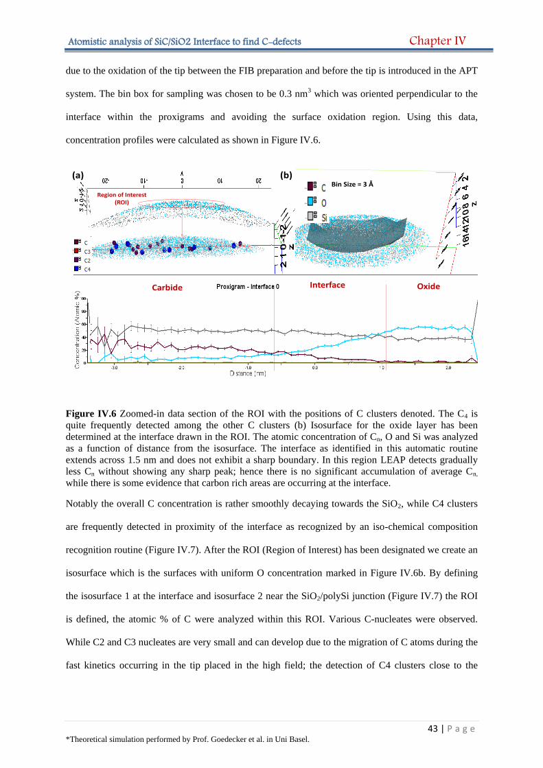
Atomistic analysis of SiC/SiO2 Interface to find C-defects Chapter IV
43 | P a g e *Theoretical simulation performed by Prof. Goedecker et al. in Uni Basel.
due to the oxidation of the tip between the FIB preparation and before the tip is introduced in the APT
system. The bin box for sampling was chosen to be 0.3 nm3 which was oriented perpendicular to the
interface within the proxigrams and avoiding the surface oxidation region. Using this data,
concentration profiles were calculated as shown in Figure IV.6.
Figure IV.6 Zoomed-in data section of the ROI with the positions of C clusters denoted. The C4 is
quite frequently detected among the other C clusters (b) Isosurface for the oxide layer has been
determined at the interface drawn in the ROI. The atomic concentration of Cn, O and Si was analyzed
as a function of distance from the isosurface. The interface as identified in this automatic routine
extends across 1.5 nm and does not exhibit a sharp boundary. In this region LEAP detects gradually
less Cn without showing any sharp peak; hence there is no significant accumulation of average Cn,
while there is some evidence that carbon rich areas are occurring at the interface.
Notably the overall C concentration is rather smoothly decaying towards the SiO2, while C4 clusters
are frequently detected in proximity of the interface as recognized by an iso-chemical composition
recognition routine (Figure IV.7). After the ROI (Region of Interest) has been designated we create an
isosurface which is the surfaces with uniform O concentration marked in Figure IV.6b. By defining
the isosurface 1 at the interface and isosurface 2 near the SiO2/polySi junction (Figure IV.7) the ROI
is defined, the atomic % of C were analyzed within this ROI. Various C-nucleates were observed.
While C2 and C3 nucleates are very small and can develop due to the migration of C atoms during the
fast kinetics occurring in the tip placed in the high field; the detection of C4 clusters close to the
Bin Size = 3 Å
OxideCarbide Interface
(a) (b)
Region of Interest(ROI)
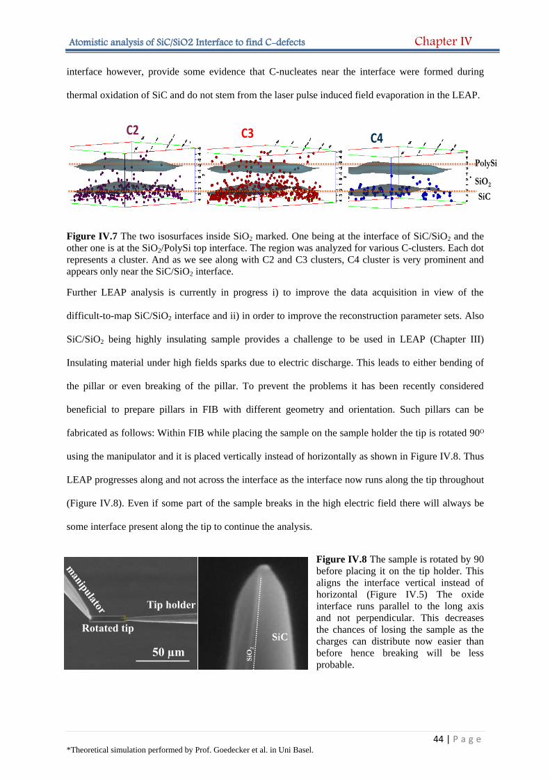
Atomistic analysis of SiC/SiO2 Interface to find C-defects Chapter IV
44 | P a g e *Theoretical simulation performed by Prof. Goedecker et al. in Uni Basel.
interface however, provide some evidence that C-nucleates near the interface were formed during
thermal oxidation of SiC and do not stem from the laser pulse induced field evaporation in the LEAP.
Figure IV.7 The two isosurfaces inside SiO2 marked. One being at the interface of SiC/SiO2 and the
other one is at the SiO2/PolySi top interface. The region was analyzed for various C-clusters. Each dot
represents a cluster. And as we see along with C2 and C3 clusters, C4 cluster is very prominent and
appears only near the SiC/SiO2 interface.
Further LEAP analysis is currently in progress i) to improve the data acquisition in view of the
difficult-to-map SiC/SiO2 interface and ii) in order to improve the reconstruction parameter sets. Also
SiC/SiO2 being highly insulating sample provides a challenge to be used in LEAP (Chapter III)
Insulating material under high fields sparks due to electric discharge. This leads to either bending of
the pillar or even breaking of the pillar. To prevent the problems it has been recently considered
beneficial to prepare pillars in FIB with different geometry and orientation. Such pillars can be
fabricated as follows: Within FIB while placing the sample on the sample holder the tip is rotated 90ᴼ
using the manipulator and it is placed vertically instead of horizontally as shown in Figure IV.8. Thus
LEAP progresses along and not across the interface as the interface now runs along the tip throughout
(Figure IV.8). Even if some part of the sample breaks in the high electric field there will always be
some interface present along the tip to continue the analysis.
Figure IV.8 The sample is rotated by 90
before placing it on the tip holder. This
aligns the interface vertical instead of
horizontal (Figure IV.5) The oxide
interface runs parallel to the long axis
and not perpendicular. This decreases
the chances of losing the sample as the
charges can distribute now easier than
before hence breaking will be less
probable.
PolySi
SiO2
SiC
C2 C3 C4
50 µm
Rotated tip
Tip holder
SiC
SiO
2
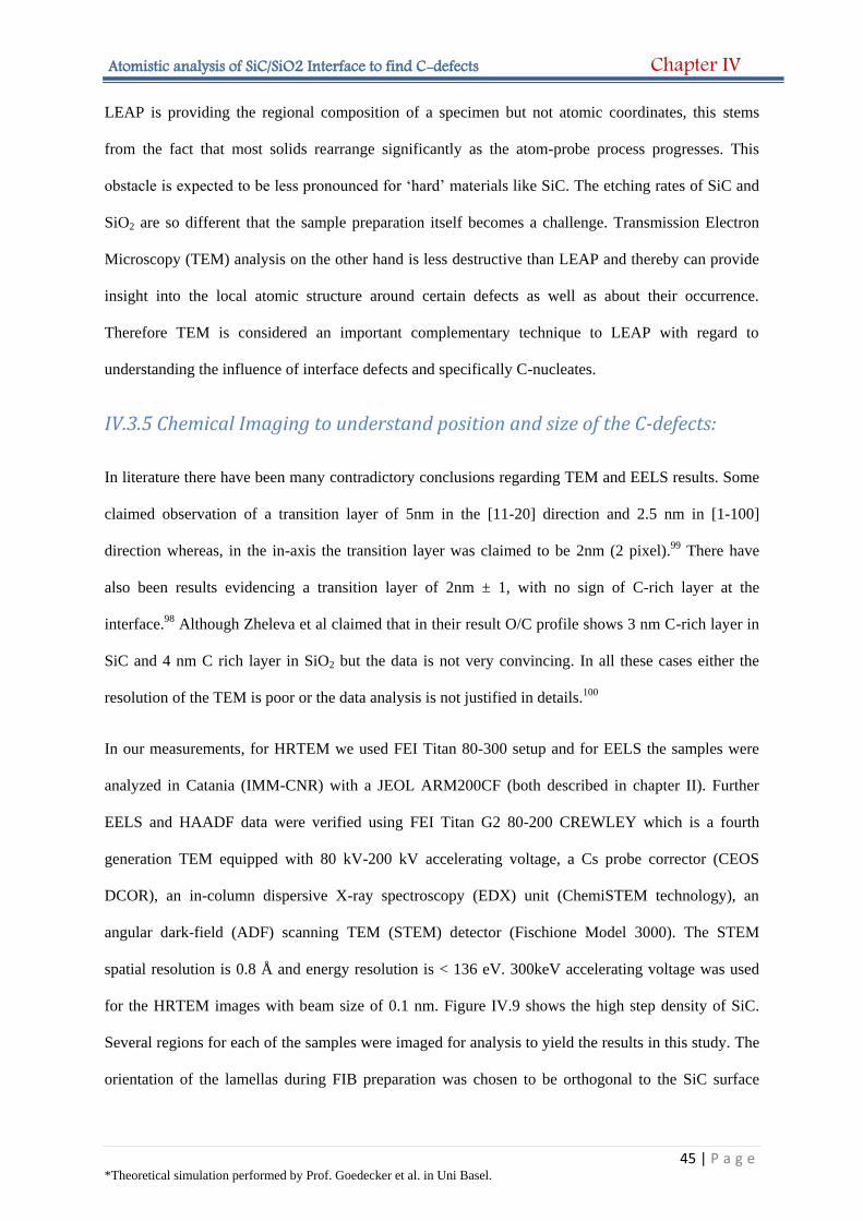
Atomistic analysis of SiC/SiO2 Interface to find C-defects Chapter IV
45 | P a g e *Theoretical simulation performed by Prof. Goedecker et al. in Uni Basel.
LEAP is providing the regional composition of a specimen but not atomic coordinates, this stems
from the fact that most solids rearrange significantly as the atom-probe process progresses. This
obstacle is expected to be less pronounced for ‘hard’ materials like SiC. The etching rates of SiC and
SiO2 are so different that the sample preparation itself becomes a challenge. Transmission Electron
Microscopy (TEM) analysis on the other hand is less destructive than LEAP and thereby can provide
insight into the local atomic structure around certain defects as well as about their occurrence.
Therefore TEM is considered an important complementary technique to LEAP with regard to
understanding the influence of interface defects and specifically C-nucleates.
IV.3.5 Chemical Imaging to understand position and size of the C-defects:
In literature there have been many contradictory conclusions regarding TEM and EELS results. Some
claimed observation of a transition layer of 5nm in the [11-20] direction and 2.5 nm in [1-100]
direction whereas, in the in-axis the transition layer was claimed to be 2nm (2 pixel).99 There have
also been results evidencing a transition layer of 2nm ± 1, with no sign of C-rich layer at the
interface.98 Although Zheleva et al claimed that in their result O/C profile shows 3 nm C-rich layer in
SiC and 4 nm C rich layer in SiO2 but the data is not very convincing. In all these cases either the
resolution of the TEM is poor or the data analysis is not justified in details.100
In our measurements, for HRTEM we used FEI Titan 80-300 setup and for EELS the samples were
analyzed in Catania (IMM-CNR) with a JEOL ARM200CF (both described in chapter II). Further
EELS and HAADF data were verified using FEI Titan G2 80-200 CREWLEY which is a fourth
generation TEM equipped with 80 kV-200 kV accelerating voltage, a Cs probe corrector (CEOS
DCOR), an in-column dispersive X-ray spectroscopy (EDX) unit (ChemiSTEM technology), an
angular dark-field (ADF) scanning TEM (STEM) detector (Fischione Model 3000). The STEM
spatial resolution is 0.8 Å and energy resolution is < 136 eV. 300keV accelerating voltage was used
for the HRTEM images with beam size of 0.1 nm. Figure IV.9 shows the high step density of SiC.
Several regions for each of the samples were imaged for analysis to yield the results in this study. The
orientation of the lamellas during FIB preparation was chosen to be orthogonal to the SiC surface
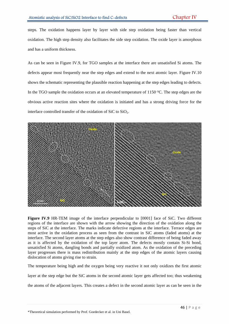
Atomistic analysis of SiC/SiO2 Interface to find C-defects Chapter IV
46 | P a g e *Theoretical simulation performed by Prof. Goedecker et al. in Uni Basel.
steps. The oxidation happens layer by layer with side step oxidation being faster than vertical
oxidation. The high step density also facilitates the side step oxidation. The oxide layer is amorphous
and has a uniform thickness.
As can be seen in Figure IV.9, for TGO samples at the interface there are unsatisfied Si atoms. The
defects appear most frequently near the step edges and extend to the next atomic layer. Figure IV.10
shows the schematic representing the plausible reaction happening at the step edges leading to defects.
In the TGO sample the oxidation occurs at an elevated temperature of 1150 ᴼC. The step edges are the
obvious active reaction sites where the oxidation is initiated and has a strong driving force for the
interface controlled transfer of the oxidation of SiC to SiO2.
Figure IV.9 HR-TEM image of the interface perpendicular to [0001] face of SiC. Two different
regions of the interface are shown with the arrow showing the direction of the oxidation along the
steps of SiC at the interface. The marks indicate defective regions at the interface. Terrace edges are
most active in the oxidation process as seen from the contrast in SiC atoms (faded atoms) at the
interface. The second layer atoms at the step edges also show contrast difference of being faded away
as it is affected by the oxidation of the top layer atom. The defects mostly contain Si-Si bond,
unsatisfied Si atoms, dangling bonds and partially oxidized atom. As the oxidation of the preceding
layer progresses there is mass redistribution mainly at the step edges of the atomic layers causing
dislocation of atoms giving rise to strain.
The temperature being high and the oxygen being very reactive it not only oxidizes the first atomic
layer at the step edge but the SiC atoms in the second atomic layer gets affected too; thus weakening
the atoms of the adjacent layers. This creates a defect in the second atomic layer as can be seen in the
SiC
Oxide
2 nm
SiC
Oxide
1 nm
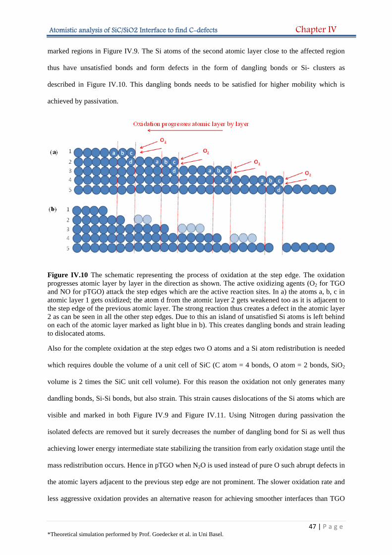
Atomistic analysis of SiC/SiO2 Interface to find C-defects Chapter IV
47 | P a g e *Theoretical simulation performed by Prof. Goedecker et al. in Uni Basel.
marked regions in Figure IV.9. The Si atoms of the second atomic layer close to the affected region
thus have unsatisfied bonds and form defects in the form of dangling bonds or Si- clusters as
described in Figure IV.10. This dangling bonds needs to be satisfied for higher mobility which is
achieved by passivation.
Figure IV.10 The schematic representing the process of oxidation at the step edge. The oxidation
progresses atomic layer by layer in the direction as shown. The active oxidizing agents (O2 for TGO
and NO for pTGO) attack the step edges which are the active reaction sites. In a) the atoms a, b, c in
atomic layer 1 gets oxidized; the atom d from the atomic layer 2 gets weakened too as it is adjacent to
the step edge of the previous atomic layer. The strong reaction thus creates a defect in the atomic layer
2 as can be seen in all the other step edges. Due to this an island of unsatisfied Si atoms is left behind
on each of the atomic layer marked as light blue in b). This creates dangling bonds and strain leading
to dislocated atoms.
Also for the complete oxidation at the step edges two O atoms and a Si atom redistribution is needed
which requires double the volume of a unit cell of SiC (C atom = 4 bonds, O atom = 2 bonds, SiO2
volume is 2 times the SiC unit cell volume). For this reason the oxidation not only generates many
dandling bonds, Si-Si bonds, but also strain. This strain causes dislocations of the Si atoms which are
visible and marked in both Figure IV.9 and Figure IV.11. Using Nitrogen during passivation the
isolated defects are removed but it surely decreases the number of dangling bond for Si as well thus
achieving lower energy intermediate state stabilizing the transition from early oxidation stage until the
mass redistribution occurs. Hence in pTGO when N2O is used instead of pure O such abrupt defects in
the atomic layers adjacent to the previous step edge are not prominent. The slower oxidation rate and
less aggressive oxidation provides an alternative reason for achieving smoother interfaces than TGO
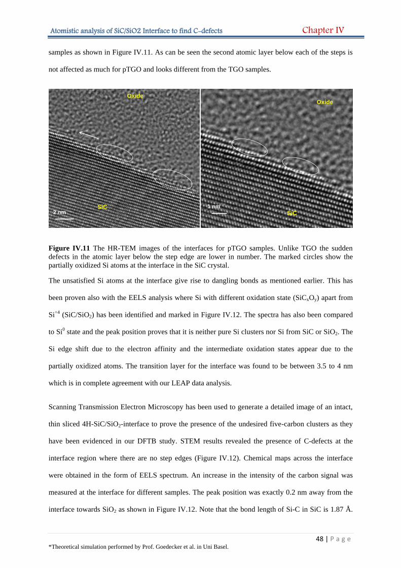
Atomistic analysis of SiC/SiO2 Interface to find C-defects Chapter IV
48 | P a g e *Theoretical simulation performed by Prof. Goedecker et al. in Uni Basel.
samples as shown in Figure IV.11. As can be seen the second atomic layer below each of the steps is
not affected as much for pTGO and looks different from the TGO samples.
Figure IV.11 The HR-TEM images of the interfaces for pTGO samples. Unlike TGO the sudden
defects in the atomic layer below the step edge are lower in number. The marked circles show the
partially oxidized Si atoms at the interface in the SiC crystal.
The unsatisfied Si atoms at the interface give rise to dangling bonds as mentioned earlier. This has
been proven also with the EELS analysis where Si with different oxidation state (SiCxOy) apart from
Si+4 (SiC/SiO2) has been identified and marked in Figure IV.12. The spectra has also been compared
to Si0 state and the peak position proves that it is neither pure Si clusters nor Si from SiC or SiO2. The
Si edge shift due to the electron affinity and the intermediate oxidation states appear due to the
partially oxidized atoms. The transition layer for the interface was found to be between 3.5 to 4 nm
which is in complete agreement with our LEAP data analysis.
Scanning Transmission Electron Microscopy has been used to generate a detailed image of an intact,
thin sliced 4H-SiC/SiO2-interface to prove the presence of the undesired five-carbon clusters as they
have been evidenced in our DFTB study. STEM results revealed the presence of C-defects at the
interface region where there are no step edges (Figure IV.12). Chemical maps across the interface
were obtained in the form of EELS spectrum. An increase in the intensity of the carbon signal was
measured at the interface for different samples. The peak position was exactly 0.2 nm away from the
interface towards SiO2 as shown in Figure IV.12. Note that the bond length of Si-C in SiC is 1.87 Å.
2 nm1 nmSiC
Oxide
SiC
Oxide
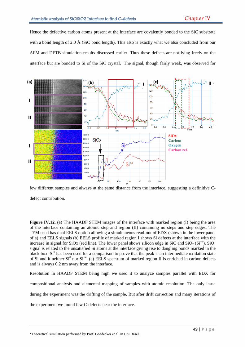
Atomistic analysis of SiC/SiO2 Interface to find C-defects Chapter IV
49 | P a g e *Theoretical simulation performed by Prof. Goedecker et al. in Uni Basel.
Hence the defective carbon atoms present at the interface are covalently bonded to the SiC substrate
with a bond length of 2.0 Å (SiC bond length). This also is exactly what we also concluded from our
AFM and DFTB simulation results discussed earlier. Thus these defects are not lying freely on the
interface but are bonded to Si of the SiC crystal. The signal, though fairly weak, was observed for
few different samples and always at the same distance from the interface, suggesting a definitive C-
defect contribution.
Figure IV.12. (a) The HAADF STEM images of the interface with marked region (I) being the area
of the interface containing an atomic step and region (II) containing no steps and step edges. The
TEM used has dual EELS option allowing a simultaneous read-out of EDX (shown in the lower panel
of a) and EELS signals (b) EELS profile of marked region I shows Si defects at the interface with the
increase in signal for SiOx (red line). The lower panel shows silicon edge in SiC and SiO2 (Si+4). SiOx
signal is related to the unsatisfied Si atoms at the interface giving rise to dangling bonds marked in the
black box. Si0 has been used for a comparison to prove that the peak is an intermediate oxidation state
of Si and it neither Si0 nor Si+4. (c) EELS spectrum of marked region II is enriched in carbon defects
and is always 0.2 nm away from the interface.
Resolution in HAADF STEM being high we used it to analyze samples parallel with EDX for
compositional analysis and elemental mapping of samples with atomic resolution. The only issue
during the experiment was the drifting of the sample. But after drift correction and many iterations of
the experiment we found few C-defects near the interface.
A
B
B
A
(a) (b) (c)
I
II
II
I
I II
nm
SiOx
Carbon
Oxygen
Carbon ref.
Atomistic analysis of SiC/SiO2 Interface to find C-defects Chapter IV
50 | P a g e *Theoretical simulation performed by Prof. Goedecker et al. in Uni Basel.
The oxide layer as discussed before is uniformly amorphous. But upon thorough monitoring of the
amorphous layer near the interface using fast fourier transform FFT, definite but modest changes in
diffraction pattern were detected. HRTEM image is built up of the wave function coming out of the
sample. So, when we apply the Fourier Transform function to the selected region of interest in the
high resolution image we have the diffraction pattern (reciprocal space) showing the symmetry of the
"lattice" fringes of the image. The number of frequencies contained in FFT corresponds to the number
of pixels in the spatial domain image, i.e. the image in the spatial and Fourier domain is of the same
size. So FFT would not pick up or show difference in pixel if there is no crystalline structure present.
In our result the signal to noise ratio being high, the intensity modulation of the diffraction pattern is
thus real in FFT. This can happen only if there is a local ordering or a crystal structure present in the
amorphous layer. Although the diffraction signal is weak but it is explicitly distinct hence the ordering
present or embedded inside the SiO2 cannot be few atoms or less than 8 to 10 atoms. This is because
FFT cannot be obtained from just one unit cell but it requires repetition of the unit cell to have the
diffraction pattern. Also to minimize any redeposition during sample preparation from Ga or SiC and
to minimize the effect of Ga damage due to FIB, samples were cleaned in a gentle Ar chamber using
Nanomill system for 20 mins. To avoid hydrocarbon which can occur as a contamination before and
during TEM analysis, samples were plasma cleaned with an Ar/O2 plasma at 50 eV for 4 min
immediately before inserting in the TEM system. Hence, for these newly prepared samples crystalline
structures from either redeposition or other sample preparation effect can be ruled out. The data
obtained is essentially due to crystalline structure which are present in the SiO2 due to the thermal
oxidation of the SiC crystal.
Following this, Inverse Fast Fourier Transform (IFFT) analysis was obtained from the diffraction
signal. IFFT is the image formation procedure by selecting specific diffraction spots in the FFT. As
seen in Figure IV.14 there is a graphitic like structure inside the amorphous oxide in the image plane.
IFFT shows the contrast difference in the data due to the atoms but does not show the actual atoms so
it is only a filtered image projection. The graphitic flake can be a result of excessive C at the interface
which could not leave as CO molecules because it is kinetically limited due to the thick oxide above.
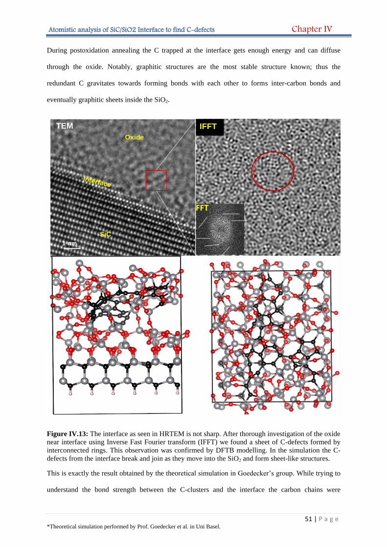
Atomistic analysis of SiC/SiO2 Interface to find C-defects Chapter IV
51 | P a g e *Theoretical simulation performed by Prof. Goedecker et al. in Uni Basel.
During postoxidation annealing the C trapped at the interface gets enough energy and can diffuse
through the oxide. Notably, graphitic structures are the most stable structure known; thus the
redundant C gravitates towards forming bonds with each other to forms inter-carbon bonds and
eventually graphitic sheets inside the SiO2.
Figure IV.13: The interface as seen in HRTEM is not sharp. After thorough investigation of the oxide
near interface using Inverse Fast Fourier transform (IFFT) we found a sheet of C-defects formed by
interconnected rings. This observation was confirmed by DFTB modelling. In the simulation the C-
defects from the interface break and join as they move into the SiO2 and form sheet-like structures.
This is exactly the result obtained by the theoretical simulation in Goedecker’s group. While trying to
understand the bond strength between the C-clusters and the interface the carbon chains were
IFFT
SiC
Oxide
1 nm
TEM
FFT
Atomistic analysis of SiC/SiO2 Interface to find C-defects Chapter IV
52 | P a g e *Theoretical simulation performed by Prof. Goedecker et al. in Uni Basel.
deliberately pushed away from the interface inside the SiO2 during minima hopping runs. In DFT, the
carbon inside the oxide was found to condensate to form quasi-planar structures as shown in
Figure.1V.13. This observation suggested that inside SiO2 the graphitic like quasi-planar carbon
structures are more stable unlike the interface where carbon liked to form nucleate in form of carbon
clusters or chains determined by the energy minima of the structures.
IV.4 Inference
In this chapter, the observed changes at the SiC/SiO2 interface were associated with the complex
oxidation at the interface leading to C-defects. C-rich nucleates at distinct locations along the
interfaces were identified by AFM, Raman, HRTEM and EELS. The high C levels at the interface are
due to the formation of excess carbon during SiC oxidation to SiO2 because the removal of CO
molecules is kinetically limited. Stoichiometric changes were also evident in the SiC layers adjacent
to the interface. In order to conciliate these defects improved passivation methods are required which
will be discussed in the following chapter.
Chapter V
Relevant parameters for improving the thermally
grown gate-oxide interface in SiC
“Quality is free. It's not a gift, but it's free. The 'unquality' things are what cost money.”
Phil Crosby
Summary
Extensive efforts have been undertaken to improve the near-interface mobility, e.g., via surface
conditioning or passivation of the SiC during interface fabrication. The oxidation of the SiC surface
marks the first step towards a passivated surface. Therefore it influences the quality of the SiC/SiO2
interface greatly and is of enormous importance. In this chapter we discuss on the interface treatment
and passivation mechanisms and on how these influence the defects at the interface.
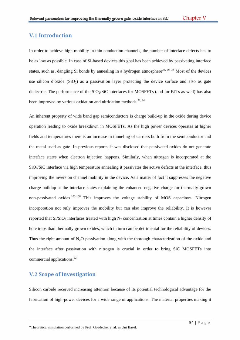
Relevant parameters for improving the thermally grown gate-oxide interface in SiC Chapter V
54 | P a g e *Theoretical simulation performed by Prof. Goedecker et al. in Uni Basel.
V.1 Introduction
In order to achieve high mobility in thin conduction channels, the number of interface defects has to
be as low as possible. In case of Si-based devices this goal has been achieved by passivating interface
states, such as, dangling Si bonds by annealing in a hydrogen atmosphere21, 26, 33 Most of the devices
use silicon dioxide (SiO2) as a passivation layer protecting the device surface and also as gate
dielectric. The performance of the SiO2/SiC interfaces for MOSFETs (and for BJTs as well) has also
been improved by various oxidation and nitridation methods.22, 24
An inherent property of wide band gap semiconductors is charge build-up in the oxide during device
operation leading to oxide breakdown in MOSFETs. As the high power devices operates at higher
fields and temperatures there is an increase in tunneling of carriers both from the semiconductor and
the metal used as gate. In previous reports, it was disclosed that passivated oxides do not generate
interface states when electron injection happens. Similarly, when nitrogen is incorporated at the
SiO2/SiC interface via high temperature annealing it passivates the active defects at the interface, thus
improving the inversion channel mobility in the device. As a matter of fact it suppresses the negative
charge buildup at the interface states explaining the enhanced negative charge for thermally grown
non-passivated oxides.101-106 This improves the voltage stability of MOS capacitors. Nitrogen
incorporation not only improves the mobility but can also improve the reliability. It is however
reported that Si/SiO2 interfaces treated with high N2 concentration at times contain a higher density of
hole traps than thermally grown oxides, which in turn can be detrimental for the reliability of devices.
Thus the right amount of N2O passivation along with the thorough characterization of the oxide and
the interface after passivation with nitrogen is crucial in order to bring SiC MOSFETs into
commercial applications.22
V.2 Scope of Investigation
Silicon carbide received increasing attention because of its potential technological advantage for the
fabrication of high-power devices for a wide range of applications. The material properties making it
Relevant parameters for improving the thermally grown gate-oxide interface in SiC Chapter V
55 | P a g e *Theoretical simulation performed by Prof. Goedecker et al. in Uni Basel.
superior to Si have been reviewed in the previous chapters. Also because of its ability to grow a
thermal gate oxide it is a preferred material of choice compared to other wide band-gap
semiconductors. The most significant improvement towards SiC MOSFET technology has been the
treatment of the interface in terms of cleaning and passivation of the gate dielectric using nitrogen as
it resulted in a tenfold reduction of active defects. The atomic-scale mechanisms behind this
passivation remain unclear, but reports convey that it removes the excess three coordinated
amorphous (polyene) C nucleates.20, 33, 70, 101, 107-110
Towards improved near-gate oxide mobilities in SiC devices it is important to investigate the impact
of SiC surface treatment either with ozone or HF and most importantly post oxidation nitrogen
treatment on the gate oxide. Ideally, the analysis should be conducted on the atomic scale. The role of
Ozone cleaning and Nitrogen passivation at the SiC/SiO2 interface have been investigated using
AFM, Raman and also by using simulations performed by Deb Sankar De in the group of the Theory
partner, Prof. S. Goedecker.
V.3 Results and Discussion
In chapter IV interface defects have been identified and C-nucleates were detected as a major Near
Interface Traps (NITs). Also we compared thermally grown oxide (TGO) with the passivated oxide
(pTGO) oxidized in an N2O environment (Chapter IV). The first remarkable difference is reflected in
the AFM morphology presented in Figure IV.1: there is a drastic reduction in the number of nucleates
at the pTGO interface compared to the non-passivated TGO interface. To further establish our results
and to investigate possible routes to reduce the carbon defect density we also treated our interface
with HF and ozone. This behavior of the carbon accumulates or defects under oxidizing atmosphere
shall be reported in the present chapter V.
V.3.1 Visualization & characterization of the interface after Ozone treatment:
The observed nucleates at the SiC/SiO2 interface emerge during the thermal oxidation as it progresses
into the wafer, as discussed in chapter IV. When the interface of the TGO (not passivated) sample is
Relevant parameters for improving the thermally grown gate-oxide interface in SiC Chapter V
56 | P a g e *Theoretical simulation performed by Prof. Goedecker et al. in Uni Basel.
ozone cleaned for 2 mins followed by HF etching a drastic reduction in the number of nucleates is
observed in the AFM micrographs. This is in agreement with an earlier report40, 80 stating that the
clusters (in our terminology nucleates) were ‘apparently composed of carbon’. This is confirmed by
the consideration that ozone, a highly oxidizing agent, will attack the C-nucleates and oxidize them
more effectively than the HF that is used to selectively etch the oxide in the preceding step. In Figure
V.1a we compare how the density of nucleates is changing for both TGO and pTGO interfaces after
HF cleaning. In Figure V.1b a TGO interface is compared before and after ozone cleaning. With only
HF cleaning (without ozone) the C-nucleates will also be reduced, but the etch rate is significantly
slower and the sample has to be dipped inside the HF etch bath for a longer time. This is because
carbon needs an oxidizing agent to get etched and the acidic water being a slower oxidizing agent than
ozone it takes a longer time to oxidize the same amount of C-nucleates at the interface.
To understand the effect of ozone on the carbon nucleates at the SiC/SiO2 interface, DFT simulations
have been performed by Goedecker’s research group. Using DFT simulations it is found that carbon
nucleates only form if no CO2 can be formed in an initial stage, i.e. in an oxygen deficient process. In
this case, CO diffuses away from the interface through the growing SiO2 layer to the surface. During
the diffusion process, the carbon atoms bind to different nearby oxygen atoms, exchanging their
partner many times before they are eventually released in form of CO or CO2 gas. Hence if the
interface is treated with ozone the C receives enough oxygen to react with. By performing MH-DFTB
simulations111 for the reaction of ozone with H-passivated carbon chains and ribbons at the SiO2
stripped interface, we confirm the experimental finding that ozone is reducing the presence of carbon
nucleates due to oxidation. The carbon nucleates in the form of clusters and chains as they have been
created by the thermal oxidation in pure oxygen ‘in-silico’ are broken into smaller pieces and CO is
released as shown in Figure V.1c and d. We therefore assign our DFT and AFM observations to the
reactive splitting of the long C-chains into smaller fragments and to their removal in the form of
defect migration via the oxide to the gas phase in the oxidation chamber.25
Relevant parameters for improving the thermally grown gate-oxide interface in SiC Chapter V
57 | P a g e *Theoretical simulation performed by Prof. Goedecker et al. in Uni Basel.
Figure V.1. Etch resistance of the nucleates in experiment and theory: The histogram analysis of the
AFM data from Figure IV.1 a) compares the nucleate density at the interface for pTGO sample
passivated in N2O to TGO non-passivated sample b) reveals the reduction of the nucleates at the TGO
interface after Ozone cleaning. The inset in b) shows the AFM morphology with reduced nucleates at
the interface of the TGO sample after ozone cleaning. c) and d) MH-DFTB simulations of a carbon
chain exposed to ozone. In c) a 5 carbon ring chain and in d) a 6 carbon ring chain are broken up by
the reaction with ozone and smaller carbon nucleates remain on the surface. Due to the Ozone
oxidation of the nucleates at the interface the carbon gets completely oxidized or breaks down to
smaller nucleates.
This DFT result is in agreement with our experimental Raman analysis in that no significant change in
the bonding state of the remaining C from bulk SiC has been observed. Only the non-SiC (defective)
carbon, recognized by the C-C bond, is reduced as these atoms get oxidized in ozone. We have
studied the intensity changes in the Raman peaks after the pure oxygen processed sample has been
cleaned using Ozone (Figure V.2). There is a decline in the Raman intensity of the carbon peak due to
the reduced number of non-SiC carbon bonds at the interface after ozone treatment. This is caused by
the removal or reduction of the average size of the C-nucleates. Further, oxygen stripped TGO
samples were also dipped in 7% HF etch for 1 min and 2 min respectively where we observed a
reduction of ≈ 5% in the Raman intensity of the carbon peaks. This result provides evidence towards
1 2 3 4 5 6 7 8 9 100
1x10⁻⁵
2x10⁻⁵
3x10⁻⁵
Den
sit
y o
f p
art
icle
s (
pe
r s
qu
are
nm
)
height (nm)
TGO HF cleaned 2 min
TGO HF+Ozone cleaned 2 min
(c) (d)
(a) (b)
1 2 3 4 5 6 7 8 9 100
1x10⁻⁵
2x10⁻⁵
3x10⁻⁵
Den
sit
y o
f p
art
icle
s (
per
sq
uare
nm
)
height (nm)
TGO HF cleaned 2 min
pTGO HF cleaned 2 min
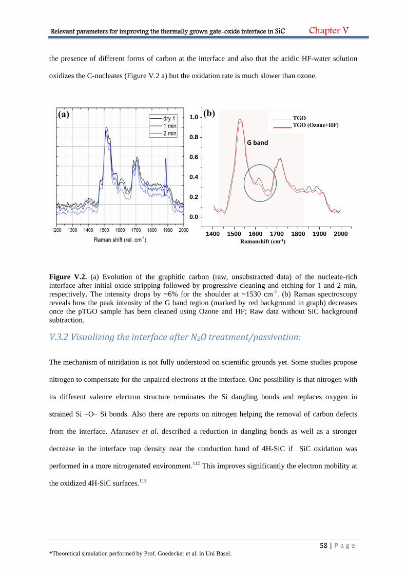
Relevant parameters for improving the thermally grown gate-oxide interface in SiC Chapter V
58 | P a g e *Theoretical simulation performed by Prof. Goedecker et al. in Uni Basel.
the presence of different forms of carbon at the interface and also that the acidic HF-water solution
oxidizes the C-nucleates (Figure V.2 a) but the oxidation rate is much slower than ozone.
Figure V.2. (a) Evolution of the graphitic carbon (raw, unsubstracted data) of the nucleate-rich
interface after initial oxide stripping followed by progressive cleaning and etching for 1 and 2 min,
respectively. The intensity drops by ~6% for the shoulder at ~1530 cm-1. (b) Raman spectroscopy
reveals how the peak intensity of the G band region (marked by red background in graph) decreases
once the pTGO sample has been cleaned using Ozone and HF; Raw data without SiC background
subtraction.
V.3.2 Visualizing the interface after N2O treatment/passivation:
The mechanism of nitridation is not fully understood on scientific grounds yet. Some studies propose
nitrogen to compensate for the unpaired electrons at the interface. One possibility is that nitrogen with
its different valence electron structure terminates the Si dangling bonds and replaces oxygen in
strained Si –O– Si bonds. Also there are reports on nitrogen helping the removal of carbon defects
from the interface. Afanasev et al. described a reduction in dangling bonds as well as a stronger
decrease in the interface trap density near the conduction band of 4H-SiC if SiC oxidation was
performed in a more nitrogenated environment.112 This improves significantly the electron mobility at
the oxidized 4H-SiC surfaces.113
1400 1500 1600 1700 1800 1900 2000
0.0
0.2
0.4
0.6
0.8
1.0
Wavenumber (cm-1)
arb
. In
ten
sit
y
DRY
DRY (ozone+HF)
G band
TGO
TGO (Ozone+HF)
Ramanshift (cm-1)
(a) (b)
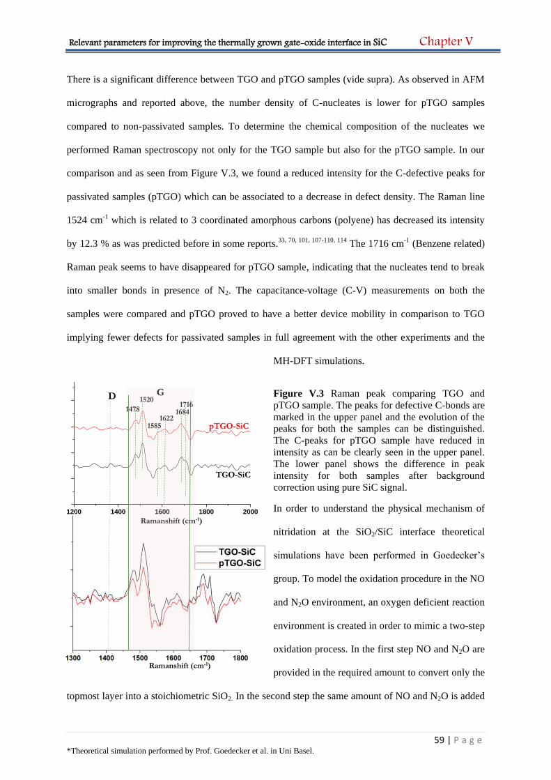
Relevant parameters for improving the thermally grown gate-oxide interface in SiC Chapter V
59 | P a g e *Theoretical simulation performed by Prof. Goedecker et al. in Uni Basel.
There is a significant difference between TGO and pTGO samples (vide supra). As observed in AFM
micrographs and reported above, the number density of C-nucleates is lower for pTGO samples
compared to non-passivated samples. To determine the chemical composition of the nucleates we
performed Raman spectroscopy not only for the TGO sample but also for the pTGO sample. In our
comparison and as seen from Figure V.3, we found a reduced intensity for the C-defective peaks for
passivated samples (pTGO) which can be associated to a decrease in defect density. The Raman line
1524 cm-1 which is related to 3 coordinated amorphous carbons (polyene) has decreased its intensity
by 12.3 % as was predicted before in some reports.33, 70, 101, 107-110, 114 The 1716 cm-1 (Benzene related)
Raman peak seems to have disappeared for pTGO sample, indicating that the nucleates tend to break
into smaller bonds in presence of N2. The capacitance-voltage (C-V) measurements on both the
samples were compared and pTGO proved to have a better device mobility in comparison to TGO
implying fewer defects for passivated samples in full agreement with the other experiments and the
MH-DFT simulations.
Figure V.3 Raman peak comparing TGO and
pTGO sample. The peaks for defective C-bonds are
marked in the upper panel and the evolution of the
peaks for both the samples can be distinguished.
The C-peaks for pTGO sample have reduced in
intensity as can be clearly seen in the upper panel.
The lower panel shows the difference in peak
intensity for both samples after background
correction using pure SiC signal.
In order to understand the physical mechanism of
nitridation at the SiO2/SiC interface theoretical
simulations have been performed in Goedecker’s
group. To model the oxidation procedure in the NO
and N2O environment, an oxygen deficient reaction
environment is created in order to mimic a two-step
oxidation process. In the first step NO and N2O are
provided in the required amount to convert only the
topmost layer into a stoichiometric SiO2. In the second step the same amount of NO and N2O is added
1200 1400 1600 1800 2000
D G
1478
1520
15851622
16841716
Ramanshift (cm-1)
Ramanshift (cm-1)
pTGO-SiC
TGO-SiC
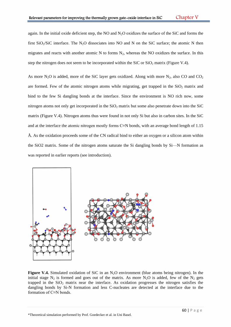
Relevant parameters for improving the thermally grown gate-oxide interface in SiC Chapter V
60 | P a g e *Theoretical simulation performed by Prof. Goedecker et al. in Uni Basel.
again. In the initial oxide deficient step, the NO and N2O oxidizes the surface of the SiC and forms the
first SiO2/SiC interface. The N2O dissociates into NO and N on the SiC surface; the atomic N then
migrates and reacts with another atomic N to forms N2, whereas the NO oxidizes the surface. In this
step the nitrogen does not seem to be incorporated within the SiC or SiO2 matrix (Figure V.4).
As more N2O is added, more of the SiC layer gets oxidized. Along with more N2, also CO and CO2
are formed. Few of the atomic nitrogen atoms while migrating, get trapped in the SiO2 matrix and
bind to the few Si dangling bonds at the interface. Since the environment is NO rich now, some
nitrogen atoms not only get incorporated in the SiO2 matrix but some also penetrate down into the SiC
matrix (Figure V.4). Nitrogen atoms thus were found in not only Si but also in carbon sites. In the SiC
and at the interface the atomic nitrogen mostly forms C≡N bonds, with an average bond length of 1.15
Å. As the oxidation proceeds some of the CN radical bind to either an oxygen or a silicon atom within
the SiO2 matrix. Some of the nitrogen atoms saturate the Si dangling bonds by Si––N formation as
was reported in earlier reports (see introduction).
Figure V.4. Simulated oxidation of SiC in an N2O environment (blue atoms being nitrogen). In the
initial stage N2 is formed and goes out of the matrix. As more N2O is added, few of the N2 gets
trapped in the SiO2 matrix near the interface. As oxidation progresses the nitrogen satisfies the
dangling bonds by Si-N formation and less C-nucleates are detected at the interface due to the
formation of C≡N bonds.
Relevant parameters for improving the thermally grown gate-oxide interface in SiC Chapter V
61 | P a g e *Theoretical simulation performed by Prof. Goedecker et al. in Uni Basel.
Xu et al. concluded that most of the N atoms tend to bind with three Si atoms,115 whereas, Umeda et
al. reported that the N donors (tetra-coordinated N) also have a tendency to occupy substitutional C
sites.116 These nitrogen atoms are observed in the channel region after post-nitridation annealing.
According to Mori et al. the simulated photoelectron intensity angular distribution (PIAD) pattern for
the atomic arrangement around N atoms is qualitatively similar with their experimentally measured
PIAD pattern.117
In our calculated structures it is observed that some of the nitrogen atoms partially replace the C
atoms in the top SiC layer and directly bond to three Si atoms, while the Si atoms bond to the
remaining C atom sites; this supports the previous experimental data discussed in chapter IV. The
average bond length is around 1.75 Å, comparable with the Si –N bond length measured in the gas
phase. The Si –N bond length has been determined in literature experimentally by photo-electron
diffraction experiments to be 1.730 ± 0.08 Å, which agrees very well with our results.118 The Si –N
bond length is shorter than the Si – C bond length and because of this difference in their bond lengths,
interfacial N causes interface strain within SiC at the SiO2/SiC interface119 as it has also been
observed in our STEM/HR-TEM results (Figure IV.11).
The formation of CN molecules suggests that only few small carbon clusters are formed at the
interface (Figure V.4) which agrees well with our Raman intensity profile (Figure V.3). However, it
leads to the presence of carbon atoms in the SiO2 matrix. Also it is observed that the formed CN
molecules eventually react with oxygen and leave as the byproduct CO as a byproduct while the
nitrogen atoms are left behind. This observation is again consistent with the experimental findings.112
The result of MH-prediction of CN and SiN formation matches perfectly with our Raman data for
pTGO samples (Figure V.5). We found the peak for C≡N around 22600 cm-1 and Si-N at 2480 cm-
1.120-122 There is also a peak at 2365 cm-1 which corresponds to the N2 Raman peak. We associate the
peak shift with the strain present in the system as is predicted due to nitrogen incorporation in a SiC
matrix. The formation of CN molecules confirms that the concentration of C-defects in pTGO is
lower. Since the mobility in pTGO samples is better it can be directly associated to the decrease in the
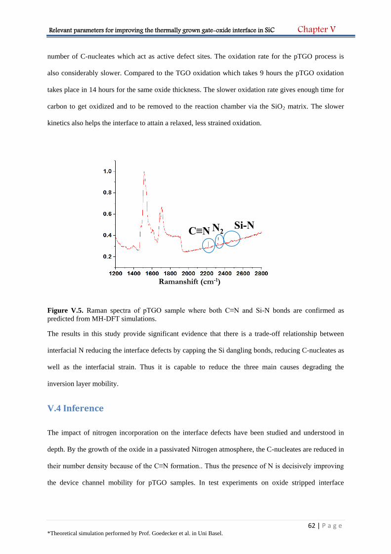
Relevant parameters for improving the thermally grown gate-oxide interface in SiC Chapter V
62 | P a g e *Theoretical simulation performed by Prof. Goedecker et al. in Uni Basel.
number of C-nucleates which act as active defect sites. The oxidation rate for the pTGO process is
also considerably slower. Compared to the TGO oxidation which takes 9 hours the pTGO oxidation
takes place in 14 hours for the same oxide thickness. The slower oxidation rate gives enough time for
carbon to get oxidized and to be removed to the reaction chamber via the SiO2 matrix. The slower
kinetics also helps the interface to attain a relaxed, less strained oxidation.
Figure V.5. Raman spectra of pTGO sample where both C≡N and Si-N bonds are confirmed as
predicted from MH-DFT simulations.
The results in this study provide significant evidence that there is a trade-off relationship between
interfacial N reducing the interface defects by capping the Si dangling bonds, reducing C-nucleates as
well as the interfacial strain. Thus it is capable to reduce the three main causes degrading the
inversion layer mobility.
V.4 Inference
The impact of nitrogen incorporation on the interface defects have been studied and understood in
depth. By the growth of the oxide in a passivated Nitrogen atmosphere, the C-nucleates are reduced in
their number density because of the C≡N formation.. Thus the presence of N is decisively improving
the device channel mobility for pTGO samples. In test experiments on oxide stripped interface
Ramanshift (cm-1)
C≡NSi-NN2

Relevant parameters for improving the thermally grown gate-oxide interface in SiC Chapter V
63 | P a g e *Theoretical simulation performed by Prof. Goedecker et al. in Uni Basel.
specimens, the interface treatment in ozone gas and HF baths for a prolonged time also reduce the
number of C-nucleates as observed in AFM micrographs and in Raman spectroscopy.

Chapter VI
Conclusion and Outlook (what’s next?)
“I think and think for months and years. Ninety-nine times, the conclusion is false. The
hundredth time I am right.”
Albert Einstein
Summary
In this work we have focused on contributing to the extensive research effort going on towards
realizing reliable SiC high power devices. Defects associated with oxide and specifically with
interfaces and interface properties have been dealt with in great details. In some cases practical
solutions to some of the issues were proposed. In this chapter all the main findings of my research
have been assembled and conclusions have been deduced on the basis of my thesis work to date.
Conclusion and Outlook (what’s next?) Chapter VI
65 | P a g e
VI.1 Conclusions and Discussions
With the data and conclusions associated with my thesis we have tried to further enrich the
understanding of the SiO2/SiC interface.
Importance of sample preparation (Chapter II and chapter III)
Sample preparation plays one of the most important roles in my thesis. The methods, the
instruments used and the derivation of all the results are a consequence of how well the sample
has been prepared. The results we obtain are thoroughly influenced by it. For STEM/ EELS/
LEAP specific sample geometries with a well-defined thickness lower than 30 nm are a must.
Higher thickness will add to the background signal significantly which will interfere with the C-
signal.
We performed our experiments on MOS capacitor chip prototypes provided by Ascatron. The
MOS capacitor has different layers of material on top of the oxide as would be for any fully
functional capacitor chip. This made the sample preparation even trickier as the etching rates for
each of this material are different. Unless proper measures are taken to safeguard homogeneous
milling with the FIB, curtaining effects compromise HRTEM/ STEM experiments. Most
importantly, a thick conducting protection layer (in our case Pt) is important.
While preparing such thin lamella as they are needed for precise chemical analysis by HAADF-
STEM, it is important to take adequate measures that no other defects are introduced into the
sample. Reports on FIB prepared samples have to be critically reviewed for their sample
preparation and preliminary characterization as they also impact the conclusiveness of STEM/
EELS/ LEAP results. This is because FIB uses Ga ions which are large in size and can create a lot
of damage to the atomic lattice and leave amorphous layers behind. In the case of our 30 nm thin
sample we observed a 20 nm amorphous layer surrounding it. For atomic resolution STEM
imaging and for reliably obtaining data and drawing conclusions, nanomilling with a gentle ion

Conclusion and Outlook (what’s next?) Chapter VI
66 | P a g e
source is imperative. After each nanomill sesssion, samples were analyzed under TEM to check if
the amorphous layer had been removed completely.
Since we are looking for nm scale C-defects it is important that the analyzing window in
STEM/HRTEM does not induce carbon into the sample regions to be analyzed. Thus, each
sample before being introduced in the chamber should be plasma cleaned. After being introduced
in the STEM/HRTEM system the sample should be allowed to stay in the vacuum chamber for an
hour. These steps help in stabilizing the sample, reduce thermal drift and also reduce carbon
formation induced by the high energy beam.
Also the voltage applied for STEM/ HRTEM plays a vital role. Since C-nucleates are small in
size and carbon is a very light element it can be easily removed if high energy beam currents are
used. For most EELS experiments an acceleration voltage of 80 kV was used. If higher voltages
were needed it was only for very short (~30 secs) time to avoid further damage to the sample.
The above mentioned conclusion regarding sample preparation was derived after many iterations and
on the basis of the experiences gained during the experimental sessions.
Atomic scale investigation of SiC/SiO2 interface (Chapter IV)
We present conclusive evidence from AFM and Raman experiments that thermal oxidation of SiC
leads to local, HF etch resistant carbon nucleates. The pearl necklace morphology indicates that
certain interface features, e.g., step bunched areas may play a role towards the defect formation.
Extensive atomistic simulations support this picture and further provide a detailed understanding
on the origin of these nucleates and on how they form predominantly at the SiC step edges. DFTB
proved their strong bond to the surrounding matrix via Si-C and O-C bonds, thus providing
evidence for nucleates being highly resistant to HF etching. Our Raman results further provide
conclusive affirmation of the presence of sp2 carbon and semicircular rings as well as of
amorphous carbon (sp3 mixed in an sp2 environment) which is different from the carbon contained
in the SiC matrix. The DFT normal modes of vibration were compared with the experimentally
Conclusion and Outlook (what’s next?) Chapter VI
67 | P a g e
observed Raman data and surprisingly 6 out of the 10 defective C-bond peaks matched. Further,
the DFT calculations also confirm the impact of the defective carbon accumulations on the
electronic structure at the interface.
Following up on the concerting evidence of the presence of C clusters chemically bonded with
non-SiC bonds at the interface we wanted to understand the C-nucleates with regards to their
exact position and composition inside the SiC/SiO2 interface. LEAP is a unique instrument where
the composition of the material can be determined with high spatial resolution (~nm). Since
LEAP is being used for the first time to investigate SiC, several iterations were required to obtain
the ideal threshold voltage of 6.7 kV for disassembling the needle shaped sample. After the 3D
chemical pillar was reconstructed, the interface and the region of interface were established. The
striking observation was that the interface was not atomically sharp and measured ≈ 1.8 nm
across. C4 clusters were also present near and at the interface. For an optimized conclusion
further measurements and statistical data analysis will be required. For this purpose new samples
have to be prepared with a completely new geometry where the oxide will be vertically running
parallel to the length of the pillar. This will help to yield the maximum data from the region of
interest before the pillar is fractured by the high field.
Chemical imaging by TEM has been used as a less destructive complimentary analytical
technique compared to LEAP, where the atomic structure to be investigated was not disintegrated
in the progress of the experiment. The HR-TEM data provides an accurate picture of how the
oxidation proceeds at the interface i.e. in a layer by layer mode. Fast thermal oxidation produces
stress and defects at the interface; this is more pronounced for TGO compared to pTGO. Also the
exact steps towards the formation of Si dangling bonds were identified. EELS at the interface
established the different oxidation states for Si atoms apart from Si+4 state. EELS results also
confirmed the presence of C nucleates at 0.2 nm from the interface which is the bond length of Si-
C. This result compliments our AFM and theory findings where we concluded that the C-
Conclusion and Outlook (what’s next?) Chapter VI
68 | P a g e
nucleates are not freely lying at the interface but rather attached to the interface via Si-bonds
making them HF etch resistant .
Further, periodic patterns within the SiO2 in near interface regions have been thoroughly
investigated using FFT/IFFT periodic filtering and analysis. Diffraction patterns appeared in
certain regions within the amorphous SiO2. This provides significant evidence that there are
regularly appearing small crystallites embedded inside the amorphous SiO2 layer. Although the
diffraction signal is weak, it is distinct. Note that such crystalline structures cannot be detected for
nucleates comprised by less than 8 to 10 atoms because FFT cannot be obtained from just a single
unit cell but it requires repetition of the unit cell to identify the diffraction pattern. IFFT result
showed graphitic sheets constituting a 5 and 6 membered C ring embedded inside the SiO2 near
the interface. DFTB simulations independently predicted the same result. The whole process of
carbon accumulation is driven by the exceptional stability of the graphitic carbon-carbon bond
which is a minority side reaction of the carbon oxidation to CO and eventually CO2. Experimental
and theoretical evidence support the conclusion that without further preventive measures graphitic
carbon condensates provide a minority phase which coexists, in particular at specific interface
locations, to the – intended -- thermal oxide. Theoretical simulation of the reaction has been
recorded providing evidence towards the atomistic trajectory / chemical pathway of the formation
of these 5 and 6 atom C-ring graphitic sheets inside the SiO2 matrix.
Interface Treatment and Passivation (Chapter V)
The difference between the passivated and non-passivated sample was prominent in the AFM
micrographs. The interface for pTGO sample had less C-nucleates attached to the Si of SiC matrix
compared to the TGO sample.
The oxygen stripped TGO interface when treated with Ozone exhibited a significantly reduced
number density of C-nucleates as evidenced by DFT, AFM and Raman. This is because ozone
being a strong oxidizing agent attacks the C-defects to oxidize them as CO and CO2. This further
proves that the nucleates identified at the TGO sample interface are indeed carbon or carbon
Conclusion and Outlook (what’s next?) Chapter VI
69 | P a g e
compounds (SiOxCy). The TGO sample, when dipped in HF etch bath for a long time,
surprisingly, showed a similar reduction in the number density of C-nucleates. This is because the
dilute HF etch solution is a milder oxidizing agent compared to ozone and the oxygen from the
water takes a longer time to oxidize the C-defects.
The Raman spectra clearly indicate the reduced intensity for C- peaks for the passivated (and
ozone etched) samples. Especially the decrease was prominent for the peaks at 1524 cm-1 and
1716 cm-1 which corresponds to 3 coordinated amorphous carbon and benzene like ring structures
respectively. This proves that nitrogen incorporation not only terminates dangling bonds but due
to the formation of CN radicals the C-nucleates fragment to either smaller defects or diminishes
altogether. MH-DFT simulations in Goedecker’s group proved that if N2O is used for oxidation
there is formation of SiN and also CN which hinders the formation of C-nucleates. This is
because nitrogen terminates and pacifies the dangling bonds for Si and renders them
electronically passive. Interestingly we found both CN and SiN peaks in our Raman spectra for
pTGO samples providing evidence for the aforementioned hypotheses.
VI.2 Outlook
Using SiC, energy savings between 17 and 33% may be attained in railway propulsion systems123 and
in other genres of high power systems. Their realistic commercialization potential, however, still
remains limited by the low channel mobility due to the high interface state density near the
conduction band. Whether cleaning and treatment of the interface has reached its limits or not,
remains to be discussed, also in view of the present results. The next step could be provided by
optimizing the gate insulator fabrication (thermal, ALD, multilayer stacking) to overcome current
limits in the channel mobility of SiC devices. Implementation of high-k gate dielectric insulators can
potentially provide further advances: For obtaining the same gate capacitance a thicker gate insulator
will be required as compared to SiO2. High-k materials have generally relatively large band gaps, such
as Al2O3, AlN, and AlON and are attractive for SiC-based MISFETs. Indeed, a high channel mobility
of 100 – 200 cm2V–1s−1 and a high breakdown electric field of 12–15 MVcm−1 have been reported
Conclusion and Outlook (what’s next?) Chapter VI
70 | P a g e
utilizing Al2O3 and AlON gate layers on planar MIS structures .124 The lower deposition temperatures
will also favor high quality interfaces and diminish interlayer diffusion. Further, by implementing
multilayer architectures for gate insulators, which is challenging, the reliability of the device may
improve. Another very advantageous development would be the implementation of trench
architectures aligned in different crystallographic directions to benefit from the anisotropy of the SiC
wafer in the shaping of the trench and in the electronic characteristics.
The present study also motivates further research to investigate the carbon accumulation mechanisms
contributing to the experimentally observed larger nucleates, and towards the role of passivating
agents. This can be achieved by using unique techniques like LEAP but the sample preparation
techniques and the operation conditions for highly insulating specimen like SiO2 have to be improved.
Also using XPS and SPM might throw new light onto the interface chemistry. Oxides can be grown
in-situ inside the vacuum and the process can be simultaneously examined using XPS or even better
Grand ARM Atomic Resolution Electron Microscope with unprecedented STEM image resolution of
55pm for atomic scale chemical imaging. Nitridation of the interface results in suppression of
electron-induced states while there can be an increase in the density of hole traps because of the
formation of SiON. Identifying the mechanisms of these two effects will be beneficial. Also by
optimizing the NO annealing the nitrogen at the interface can be controlled so that both interface state
densities and hole trap densities are curtailed. If excess nitrogen is avoided at the interface then along
with passivation there will be enhancement in the reliability of SiC oxide-based devices. Nitrogen
accumulation at the interface depends on the oxidation rate and the dosage of Nitrogen and NO
annealing time. In the oxide of the silicon nitrogen can be incorporated as well to reduce gate
leakage.125-126 It will therefore be useful if the properties of NO-annealed SiO2/SiC structures can be
studied within the wider examined Si framework.
Studying different oxidation rate and oxidation pressure in order to understand the kinetics of the
oxide growth might also be beneficial. With higher oxygen pressure the temperature and the time
required for oxide growth can be lowered. This will lower the industrial oxide growth cost. The defect

Conclusion and Outlook (what’s next?) Chapter VI
71 | P a g e
formation mechanisms however has to be kept in mind as well and can be further investigated not
only with respect to oxide pressure but also with varying oxide thicknesses. In the end a very critical
and difficult to predict issue is whether deposited or native thermal oxidation will win the race for
cost/ performance optimization as this will certainly affect the impact of SiC in different markets for
power semiconductor and related devices.

Bibliography
1. Braun, F., Ueber die Stromleitung durch Schwefelmetalle. Annalen der Physik 1875, 229 (12), 556-
563.
2. Wilson, T. G., The evolution of power electronics. IEEE transactions on power electronics 2000, 15
(3), 439-446.
3. Erickson, R. W.; Maksimovic, D., Fundamentals of power electronics. Springer Science & Business
Media: 2007.
4. Baliga, B. J., Fundamentals of power semiconductor devices. Springer Science & Business Media:
2010.
5. Siddiqui, A.; Elgabra, H.; Singh, S., The Current Status and the Future Prospects of Surface Passivation
in 4H-SiC Transistors. IEEE Transactions on Device and Materials Reliability 2016, 16 (3), 419-428.
6. Kularatna, N., Power electronics design handbook: low-power components and applications. Elsevier:
1998.
7. M. M. Atalla, E. T. a. E. J. S. Stabilization of silicon surfaces by thermally grown oxides. (accessed 3).
8. Östling, M.; Ghandi, R.; Zetterling, C.-M., SiC power devices - Present status, applications and future
perspective. 2011; p 10-15.
9. Šimonka, V.; Hössinger, A.; Weinbub, J.; Selberherr, S., Growth rates of dry thermal oxidation of 4H-
silicon carbide. Journal of Applied Physics 2016, 120 (13), 135705.
10. Kimoto, T.; Cooper, J. A., Fundamentals of Silicon Carbide Technology: Growth, Characterization,
Devices and Applications. John Wiley & Sons: 2014.
11. Wright, N. G.; Horsfall, A. B.; Vassilevski, K., Prospects for SiC electronics and sensors. Materials
today 2008, 11 (1-2), 16-21.
12. Brezeanu, G. In Silicon carbide (SiC): a short history. an analytical approach for SiC power device
design, Semiconductor Conference, 2005. CAS 2005 Proceedings. 2005 International, IEEE: 2005; pp 345-348.
13. Ortiz-Rodriguez, J.; Duong, T.; Rivera-Lopez, A.; Hefner, A. In High-voltage, high-frequency SiC
power MOSFETs model validation, Power Electronics Specialists Conference, 2007. PESC 2007. IEEE, IEEE:
2007; pp 1018-1022.
14. Cooper, J. A.; Melloch, M. R.; Singh, R.; Agarwal, A.; Palmour, J. W., Status and prospects for SiC
power MOSFETs. IEEE Transactions on Electron Devices 2002, 49 (4), 658-664.
15. Ueda, T.; Nishino, H.; Matsunami, H., Crystal growth of SiC by step-controlled epitaxy. Journal of
Crystal Growth 1990, 104 (3), 695-700.
16. SiC Technology Is Proving Its Value. CS compound semiconductors 2015.
Bibliography
74 | P a g e
17. New York State Department of Environmental Conservation, Guidelines for conducting bird and bat
studies at commercial wind energy projects. Division of Fish Wildlife and Marine Resources, Ed. Albany, NY,
2009.
18. Kumar Gupta, S.; Akhtar, J., Thermal Oxidation of Silicon Carbide (SiC) � Experimentally Observed
Facts. 2011.
19. Jernigan, G. G.; Stahlbush, R. E.; Das, M. K.; Cooper, J. A.; Lipkin, L. A., Interfacial differences
between SiO2 grown on 6H-SiC and on Si(100). Applied Physics Letters 1999, 74 (10), 1448-1450.
20. Afanas’ev, V.; Ciobanu, F.; Pensl, G.; Stesmans, A., Contributions to the density of interface states in
SiC MOS structures. In Silicon Carbide, Springer: 2004, pp 343-371.
21. Afanasev, V.; Bassler, M.; Pensl, G.; Schulz, M., Intrinsic SiC/SiO2 interface states. physica status
solidi (a) 1997, 162 (1), 321-337.
22. Rozen, J. ELECTRONIC PROPERTIES AND RELIABILITY OF THE SiO2/SiC INTERFACE.
Thesis, Vanderbilt University
Faculty of the Graduate School of Vanderbilt University, 2008.
23. Plummer, J. D.; Michael, D., Deal, and Peter B. Griffin, Silicon VLSI Technology. Prentice Hall: 2000.
24. Constant, A.; Camara, N.; Godignon, P.; Camassel, J., Benefit of H 2 surface pretreatment for 4 H-SiC
oxynitridation using N 2 O and rapid thermal processing steps. Applied Physics Letters 2009, 94 (6), 063508.
25. Pippel, E.; Woltersdorf, J.; Ólafsson, H. Ö.; Sveinbjörnsson, E. Ö., Interfaces between 4H-SiC and Si O
2: Microstructure, nanochemistry, and near-interface traps. Journal of applied physics 2005, 97 (3), 034302.
26. Campi, J.; Shi, Y.; Luo, Y.; Yan, F.; Zhao, J. H., Study of interface state density and effective oxide
charge in post-metallization annealed SiO/sub 2/-SiC structures. IEEE Transactions on Electron Devices 1999,
46 (3), 511-519.
27. Chang, K.; Nuhfer, N.; Porter, L.; Wahab, Q., High-carbon concentrations at the silicon dioxide–silicon
carbide interface identified by electron energy loss spectroscopy. Applied Physics Letters 2000, 77 (14), 2186-
2188.
28. Suzuki, S.; Harada, S.; Kosugi, R.; Senzaki, J.; Cho, W.-j.; Fukuda, K., Correlation between channel
mobility and shallow interface traps in SiC metal–oxide–semiconductor field-effect transistors. Journal of
applied physics 2002, 92 (10), 6230-6234.
29. Shiraishi, K.; Chokawa, K.; Kamiya, K.; Kato, S.; Endo, K.; Araidai, M. In The First Principles
Investigation of SiC/SiO2 Interfaces Obtained by Thermal Oxidation, Meeting Abstracts, The Electrochemical
Society: 2014; pp 2086-2086.
30. Park, C.; Cheong, B.-H.; Lee, K.-H.; Chang, K., Structural and electronic properties of cubic, 2H, 4H,
and 6H SiC. Physical Review B 1994, 49 (7), 4485.
31. Lohrmann, A.; Castelletto, S.; Klein, J.; Ohshima, T.; Bosi, M.; Negri, M.; Lau, D.; Gibson, B.; Prawer,
S.; McCallum, J., Activation and control of visible single defects in 4H-, 6H-, and 3C-SiC by oxidation. Applied
Physics Letters 2016, 108 (2), 021107.
32. Moghadam, H. A.; Dimitrijev, S.; Han, J.; Haasmann, D., Active defects in MOS devices on 4H-SiC: A
critical review. Microelectronics Reliability 2016, 60, 1-9.
Bibliography
75 | P a g e
33. Wang, S.; Dhar, S.; Wang, S.-r.; Ahyi, A.; Franceschetti, A.; Williams, J.; Feldman, L. C.; Pantelides,
S. T., Bonding at the SiC− SiO 2 Interface and the effects of nitrogen and hydrogen. Physical review letters
2007, 98 (2), 026101.
34. Senzaki, J.; Kojima, K.; Harada, S.; Kosugi, R.; Suzuki, S.; Suzuki, T.; Fukuda, K., Excellent effects of
hydrogen postoxidation annealing on inversion channel mobility of 4H-SiC MOSFET fabricated on (11 2 0)
face. IEEE Electron Device Letters 2002, 23 (1), 13-15.
35. I. A. Khan, J. A. C., T. Isaacs-Smith, J. R. Williams, and L. C. Feldman, Technical Program of 2002
Electronic Materials Conference 2002.
36. Tan, J.; Cooper, J. A.; Melloch, M. R., High-voltage accumulation-layer UMOSFET's in 4H-SiC. IEEE
Electron Device Letters 1998, 19 (12), 487-489.
37. Szilágyi, E.; Petrik, P.; Lohner, T.; Koós, A. A.; Fried, M.; Battistig, G., Oxidation of SiC investigated
by ellipsometry and Rutherford backscattering spectrometry. Journal of Applied Physics 2008, 104 (1), 014903.
38. M. Mooney, P.; Jiang, Z.; Basile, A.; Zheng, Y.; Dhar, S., Effects of antimony (Sb) on electron trapping
near SiO2/4H-SiC interfaces. 2016; Vol. 120, p 034503.
39. Yano, H.; Nakao, H.; Mikami, H.; Hatayama, T.; Uraoka, Y.; Fuyuki, T., Anomalously anisotropic
channel mobility on trench sidewalls in 4H-SiC trench-gate metal-oxide-semiconductor field-effect transistors
fabricated on 8° off substrates. Applied Physics Letters 2007, 90 (4), 042102.
40. Afanas' ev, V.; Stesmans, A.; Harris, C. I. In Observation of carbon clusters at the 4H-SiC/SiO2
interface, Materials Science Forum, Trans Tech Publications: 1998; pp 857-860.
41. Virojanadara, C. J., L. I., Oxidation studies of 4H-SiC( 0 0 0 1 ) and ( 0 0 0 1¯) Surface Science 2002,
505 (1-2,), 358-366.
42. Morales-García, Á.; Valero, R.; Illas, F., An Empirical, yet Practical Way To Predict the Band Gap in
Solids by Using Density Functional Band Structure Calculations. The Journal of Physical Chemistry C 2017,
121 (34), 18862-18866.
43. Wartewig, P. D. S., IR and Raman Spectroscopy: Fundamental Processing. Wiley Online Library:
2005.
44. Rimini, E., Ion implantation: basics to device fabrication. Springer Science & Business Media: 1994;
Vol. 293.
45. Williams D.B., C. C. B., The Transmission Electron Microscope. In: Transmission Electron
Microscopy. Springer, Boston, MA 1996.
46. Goldstein, J., ed. , Practical scanning electron microscopy: electron and ion microprobe analysis.
Springer Science & Business Media: 2012.
47. Thust, A.; Barthel, J.; Tillmann, K., FEI Titan 80-300 TEM. Journal of large-scale research facilities
JLSRF 2016, 2, 41.
48. Gault, B., et al., Atom probe microscopy. Springer Science & Business Media: 2012; Vol. 160.
49. Larson, D. J.; Prosa, T.; Ulfig, R. M.; Geiser, B. P.; Kelly, T. F., Local electrode atom probe
tomography. New York, US: Springer Science 2013.
Bibliography
76 | P a g e
50. Knaup, J. M.; Deák, P.; Frauenheim, T.; Gali, A.; Hajnal, Z.; Choyke, W., Defects in SiO 2 as the
possible origin of near interface traps in the SiC∕ SiO 2 system: A systematic theoretical study. Physical Review
B 2005, 72 (11), 115323.
51. Perdew, J. P.; Burke, K.; Ernzerhof, M., Generalized gradient approximation made simple. Physical
review letters 1996, 77 (18), 3865.
52. Lely., J. A., Darstellung von Einkristallen von Silicium Carbid und Beherrschung
von Art und Menge der eingebauten Verunreinigungen. Deutschen Keramischen Gesellschaft, 1955, 32, 229–
236.
53. Tairov, Y. M.; Tsvetkov, V. F., Investigation of growth processes of ingots of silicon carbide single
crystals. Journal of Crystal Growth 1978, 43 (2), 209-212.
54. Munding, A., Interconnect technology for three-dimensional chip integration. Cuvillier Verlag,: 2007.
55. Hong, M. H.; Samant, A. V.; Pirouz, P., Stacking fault energy of 6H-SiC and 4H-SiC single crystals.
Philosophical Magazine A 2000, 80 (4), 919-935.
56. Mikhaylov, A. I.; Afanasyev, A. V.; Luchinin, V. V.; Reshanov, S. A.; Schöner, A.; Knoll, L.;
Minamisawa, R. A.; Alfieri, G.; Bartolf, H., Tailoring the 4H-SiC/SiO2 MOS-interface for SiC-based power
switches. Japanese Journal of Applied Physics 2016, 55 (8S2), 08PC04.
57. Furukawa, Y.; Nakajima, K., Advances in crystal growth research. Elsevier: 2001.
58. Borowicz, P.; Gutt, T.; Małachowski, T.; Latek, M., Carbonic inclusions on SiC/SiO2 interface
investigated with Raman Scattering. Diamond and Related Materials 2011, 20 (5-6), 665-674.
59. Makowska-Janusik, M.; Kassiba, A.; Bouclé, J.; Bardeau, J.; Kodjikian, S.; Désert, A., Vibrational
density of states in silicon carbide nanoparticles: experiments and numerical simulations. Journal of Physics:
Condensed Matter 2005, 17 (33), 5101.
60. Saxey, D. W.; Cairney, J. M.; McGrouther, D.; Honma, T.; Ringer, S. P., Atom probe specimen
fabrication methods using a dual FIB/SEM. Ultramicroscopy 2007, 107 (9), 756-760.
61. Goedecker, S.; Hellmann, W.; Lenosky, T., Global minimum determination of the Born-Oppenheimer
surface within density functional theory. Physical review letters 2005, 95 (5), 055501.
62. Goedecker, S.; Deutsch, T.; Billard, L., A Fourfold Coordinated Point Defect in Silicon. Physical
Review Letters 2002, 88 (23), 235501.
63. Krukau, A. V.; Vydrov, O. A.; Izmaylov, A. F.; Scuseria, G. E., Influence of the exchange screening
parameter on the performance of screened hybrid functionals. The Journal of Chemical Physics 2006, 125 (22),
224106.
64. Goedecker, S., Minima hopping: An efficient search method for the global minimum of the potential
energy surface of complex molecular systems. The Journal of chemical physics 2004, 120 (21), 9911-9917.
65. Schaefer, B.; Alireza Ghasemi, S.; Roy, S.; Goedecker, S., Stabilized quasi-Newton optimization of
noisy potential energy surfaces. The Journal of chemical physics 2015, 142 (3), 034112.
66. Aradi, B.; Hourahine, B.; Frauenheim, T., DFTB+, a sparse matrix-based implementation of the DFTB
method. The Journal of Physical Chemistry A 2007, 111 (26), 5678-5684.
67. Rauls, E.; Elsner, J.; Gutierrez, R.; Frauenheim, T., Stoichiometric and non-stoichiometric (1010) and
(1120) surfaces in 2H–SiC: a theoretical study. Solid state communications 1999, 111 (8), 459-464.
Bibliography
77 | P a g e
68. Köhler, C.; Hajnal, Z.; Deák, P.; Frauenheim, T.; Suhai, S., Theoretical investigation of carbon defects
and diffusion in α-quartz. Physical Review B 2001, 64 (8), 085333.
69. Kodigala, S. R.; Chattopadhyay, S.; Overton, C.; Ardoin, I.; Gordon, B.; Johnstone, D.; Roy, D.;
Barone, D., Growth and surface analysis of SiO2 on 4H-SiC for MOS devices. Applied Surface Science 2015,
330, 465-475.
70. S. Dimitrijev, H. B. H., P. Tanner, K. Y. Cheong, and J. Han, Silicon
Carbide: Recent Major Advances. Springer, Boston, MA 2004, 373–386.
71. Dimitrijev, S.; Jamet, P., Advances in SiC power MOSFET technology. Microelectronics Reliability
2003, 43 (2), 225-233.
72. Sun, J.; Hannon, J. B.; Tromp, R. M.; Pohl, K., Highly uniform step and terrace structures on SiC
(0001) surfaces. IBM Journal of Research and Development 2011, 55 (4), 7: 1-7: 6.
73. Starke, U.; Bernhardt, J.; Schardt, J.; Heinz, K., SiC surface reconstruction: Relevancy of atomic
structure for growth technology. Surface Review and Letters 1999, 6 (06), 1129-1141.
74. Kimoto, T.; Itoh, A.; Matsunami, H., Step‐controlled epitaxial growth of high‐quality SiC layers.
physica status solidi (b) 1997, 202 (1), 247-262.
75. Epler, J.; Jung, T.; Schweizer, H., Evolution of monolayer terrace topography on (100) GaAs annealed
under an arsine/hydrogen ambient. Applied physics letters 1993, 62 (2), 143-145.
76. Bokor, J., Ultrafast Dynamics at Semiconductor and Metal Surfaces. Science 1989, 246 (4934), 1130-
1134.
77. Liu, P.; Li, G.; Duscher, G.; Sharma, Y. K.; Ahyi, A. C.; Isaacs-Smith, T.; Williams, J. R.; Dhar, S.,
Roughness of the SiC/SiO2 vicinal interface and atomic structure of the transition layers. Journal of Vacuum
Science & Technology A 2014, 32 (6), 060603.
78. Phelps, G.; Wright, N.; Chester, E.; Johnson, C.; O'Neill, A., Step bunching fabrication constraints in
silicon carbide. Semiconductor science and technology 2002, 17 (5), L17.
79. Sakai, T.; Hemmi, M.; Murata, Y.; Yamakami, T.; Hayashibe, R.; Onuma, Y.; Kamimura, K. In Effect
of Direct Nitridation of 4H-SiC Surface on MOS Interface States, Materials Science Forum, Trans Tech Publ:
2012; pp 725-728.
80. Harris, C.; Afanas' ev, V., SiO2 as an insulator for SiC devices. Microelectronic engineering 1997, 36
(1-4), 167-174.
81. Raj, R.; Terauds, K., Bubble nucleation during oxidation of SiC. Journal of the American Ceramic
Society 2015, 98 (8), 2579-2586.
82. Radić, N.; Pivac, B.; Meinardi, F.; Koch, T., Raman study of carbon clusters in W–C thin films.
Materials Science and Engineering: A 2005, 396 (1-2), 290-295.
83. Schwan, J.; Ulrich, S.; Batori, V.; Ehrhardt, H.; Silva, S., Raman spectroscopy on amorphous carbon
films. Journal of Applied Physics 1996, 80 (1), 440-447.
84. Chen, Z.; Zhao, J.; Yano, T.; Ooie, T.; Yoneda, M.; Sakakibara, J., Observation of sp 3 bonding in
tetrahedral amorphous carbon using visible Raman spectroscopy. Journal of Applied Physics 2000, 88 (5), 2305-
2308.
Bibliography
78 | P a g e
85. Ferrari, A. C.; Robertson, J., Interpretation of Raman spectra of disordered and amorphous carbon.
Physical Review B 2000, 61 (20), 14095-14107.
86. Das, A.; Chakraborty, B.; Sood, A., Raman spectroscopy of graphene on different substrates and
influence of defects. Bulletin of Materials Science 2008, 31 (3), 579-584.
87. Ferrari, A. C.; Robertson, J., Raman spectroscopy of amorphous, nanostructured, diamond–like carbon,
and nanodiamond. Philosophical Transactions of the Royal Society of London A: Mathematical, Physical and
Engineering Sciences 2004, 362 (1824), 2477-2512.
88. Shi, J.; Shi, X.; Sun, Z.; Liu, E.; Tay, B.; Lau, S., Ultraviolet and visible Raman studies of nitrogenated
tetrahedral amorphous carbon films. Thin solid films 2000, 366 (1-2), 169-174.
89. Maintz, S.; Deringer, V. L.; Tchougréeff, A. L.; Dronskowski, R., Analytic projection from plane‐wave
and PAW wavefunctions and application to chemical‐bonding analysis in solids. Journal of computational
chemistry 2013, 34 (29), 2557-2567.
90. Maintz, S.; Deringer, V. L.; Tchougréeff, A. L.; Dronskowski, R., LOBSTER: A tool to extract
chemical bonding from plane‐wave based DFT. Journal of computational chemistry 2016, 37 (11), 1030-1035.
91. Deringer, V. L.; Tchougréeff, A. L.; Dronskowski, R., Crystal orbital Hamilton population (COHP)
analysis as projected from plane-wave basis sets. The Journal of Physical Chemistry A 2011, 115 (21), 5461-
5466.
92. Dronskowski, R.; Bloechl, P. E., Crystal orbital Hamilton populations (COHP): energy-resolved
visualization of chemical bonding in solids based on density-functional calculations. The Journal of Physical
Chemistry 1993, 97 (33), 8617-8624.
93. Gavrikov, A.; Knizhnik, A.; Safonov, A.; Scherbinin, A.; Bagatur’yants, A.; Potapkin, B.; Chatterjee,
A.; Matocha, K., First-principles-based investigation of kinetic mechanism of SiC (0001) dry oxidation
including defect generation and passivation. Journal of Applied Physics 2008, 104 (9), 093508.
94. Devynck, F.; Alkauskas, A.; Broqvist, P.; Pasquarello, A., Defect levels of carbon-related defects at the
SiC/SiO 2 interface from hybrid functionals. Physical Review B 2011, 83 (19), 195319.
95. Salemi, S.; Goldsman, N.; Ettisserry, D.; Akturk, A.; Lelis, A., The effect of defects and their
passivation on the density of states of the 4H-silicon-carbide/silicon-dioxide interface. Journal of Applied
Physics 2013, 113 (5), 053703.
96. Devynck, F.; Giustino, F.; Broqvist, P.; Pasquarello, A., Structural and electronic properties of an
abrupt 4 H− SiC (0001)∕ SiO 2 interface model: Classical molecular dynamics simulations and density
functional calculations. Physical Review B 2007, 76 (7), 075351.
97. Bassler, M.; Pensl, G.; Afanas' ev, V., “Carbon cluster model” for electronic states at SiCSiO2
interfaces. Diamond and Related Materials 1997, 6 (10), 1472-1475.
98. Beltrán, A. M.; Duguay, S.; Strenger, C.; Bauer, A. J.; Cristiano, F.; Schamm-Chardon, S., Atomic
scale characterization of SiO2/4H-SiC interfaces in MOSFETs devices. Solid State Communications 2015, 221,
28-32.
99. Liu, G.; Tuttle, B. R.; Dhar, S., Silicon carbide: A unique platform for metal-oxide-semiconductor
physics. Applied Physics Reviews 2015, 2 (2), 021307.
100. Zheleva, T.; Lelis, A.; Duscher, G.; Liu, F.; Levin, I.; Das, M., Transition layers at the SiO2∕SiC
interface. Applied Physics Letters 2008, 93 (2), 022108.
Bibliography
79 | P a g e
101. Hui-Feng, L.; Dimitrijev, S.; Harrison, H. B., Improved reliability of NO-nitrided SiO2 grown on p-
type 4H-SiC. IEEE Electron Device Letters 1998, 19 (8), 279-281.
102. Li, H.-F.; Dimitrijev, S.; Sweatman, D.; Harrison, H. B., Analysis of Fowler–Nordheim injection in NO
nitrided gate oxide grown on n-type 4H–SiC. Microelectronics Reliability 2000, 40 (2), 283-286.
103. Li, H.-f.; Dimitrijev, S.; Sweatman, D.; Harrison, H. B.; Tanner, P.; Feil, B., Investigation of nitric
oxide and Ar annealed SiO2/SiC interfaces by x-ray photoelectron spectroscopy. Journal of Applied Physics
1999, 86 (8), 4316-4321.
104. Johnson, C.; Wright, N.; Uren, M.; Hilton, K.; Rahimo, M.; Hinchley, D.; Knights, A.; Morrison, D.;
Horsfall, A.; Ortolland, S., Recent progress and current issues in SiC semiconductor devices for power
applications. IEE Proceedings-Circuits, Devices and Systems 2001, 148 (2), 101-108.
105. Phelps, G.; Wright, N.; Chester, E.; Johnson, C.; O’Neill, A.; Ortolland, S.; Horsfall, A.; Vassilevski,
K.; Gwilliam, R.; Coleman, P., Enhanced nitrogen diffusion in 4H-SiC. Applied physics letters 2002, 80 (2),
228-230.
106. Wright, N. G.; Morrison, D.; Johnson, C. M.; O'Neill, A. G. In Electrothermal simulation of 4H-SiC
power devices, Materials Science Forum, Aedermannsdorf, Switzerland: Trans Tech Publications, 1984-: 1998;
pp 917-920.
107. Chung, G. Y.; Tin, C. C.; Williams, J. R.; McDonald, K.; Ventra, M. D.; Pantelides, S. T.; Feldman, L.
C.; Weller, R. A., Effect of nitric oxide annealing on the interface trap densities near the band edges in the 4H
polytype of silicon carbide. Applied Physics Letters 2000, 76 (13), 1713-1715.
108. Jamet, P.; Dimitrijev, S.; Tanner, P., Effects of nitridation in gate oxides grown on 4H-SiC. Journal of
Applied Physics 2001, 90 (10), 5058-5063.
109. McDonald, K.; Weller, R. A.; Pantelides, S. T.; Feldman, L. C.; Chung, G. Y.; Tin, C. C.; Williams, J.
R., Characterization and modeling of the nitrogen passivation of interface traps in SiO2/4H–SiC. Journal of
Applied Physics 2003, 93 (5), 2719-2722.
110. Deák, P.; Hornos, T.; Thill, C.; Knaup, J.; Gali, A.; Frauenheim, T., The Mechanism of Interface State
Passivation by NO. Materials Science Forum 2007, 556-557, 541-544.
111. Amsler, M.; Goedecker, S., Crystal structure prediction using the minima hopping method. The Journal
of chemical physics 2010, 133 (22), 224104.
112. Afanas’ev, V. V.; Stesmans, A.; Ciobanu, F.; Pensl, G.; Cheong, K. Y.; Dimitrijev, S., Mechanisms
responsible for improvement of 4H–SiC/SiO2 interface properties by nitridation. Applied Physics Letters 2003,
82 (4), 568-570.
113. Schörner, R.; Friedrichs, P.; Peters, D.; Stephani, D.; Dimitrijev, S.; Jamet, P., Enhanced channel
mobility of 4H–SiC metal–oxide–semiconductor transistors fabricated with standard polycrystalline silicon
technology and gate-oxide nitridation. Applied Physics Letters 2002, 80 (22), 4253-4255.
114. Williams, J.; Chung, G.; Tin, C.; McDonald, K.; Farmer, D.; Chanana, R.; Weller, R.; Pantelides, S.;
Holland, O.; Das, M., Nitrogen passivation of the interface states near the conduction band edge in 4H-silicon
carbide. MRS Online Proceedings Library Archive 2000, 640.
115. Xu, Y.; Zhu, X.; Lee, H.; Xu, C.; Shubeita, S.; Ahyi, A.; Sharma, Y.; Williams, J.; Lu, W.; Ceesay, S.,
Atomic state and characterization of nitrogen at the SiC/SiO2 interface. Journal of Applied Physics 2014, 115
(3), 033502.
Bibliography
80 | P a g e
116. Umeda, T.; Esaki, K.; Kosugi, R.; Fukuda, K.; Ohshima, T.; Morishita, N.; Isoya, J., Behavior of
nitrogen atoms in SiC-SiO2 interfaces studied by electrically detected magnetic resonance. Applied physics
letters 2011, 99 (14), 142105.
117. Mori, D.; Oyama, Y.; Hirose, T.; Muro, T.; Matsui, F., Local structural determination of N at SiO2/SiC
(000 1¯) interfaces by photoelectron diffraction. Applied Physics Letters 2017, 111 (20), 201603.
118. Franco, N.; Avila, J.; Davila, M.; Asensio, M.; Woodruff, D.; Schaff, O.; Fernandez, V.; Schindler, K.;
Bradshaw, A., Structure determination of using scanned-energy mode photoelectron diffraction. Journal of
Physics: Condensed Matter 1997, 9 (40), 8419.
119. Houston Dycus, J.; Xu, W.; Lichtenwalner, D. J.; Hull, B.; Palmour, J. W.; LeBeau, J. M., Structure
and chemistry of passivated SiC/SiO2 interfaces. Applied Physics Letters 2016, 108 (20), 201607.
120. Grazia Giorgini, M.; Arcioni, A.; Polizzi, C.; Musso, M.; Ottaviani, P., Relaxation processes of the
liquid crystal ME6N in the isotropic phase studied by Raman scattering experiments. 2004; Vol. 120, p 4969-
79.
121. Stair, P. C., The Application of UV Raman Spectroscopy for the Characterization of Catalysts and
Catalytic Reactions. In Advances in Catalysis, Gates, B. C.; Knözinger, H., Eds. Academic Press: 2007, pp 75-
98.
122. Dhakal, A.; Wuytens, P.; Peyskens, F.; Subramanian, A. Z.; Thomas, N. L.; Baets, R., Silicon-nitride
waveguides for on-chip Raman spectroscopy. SPIE: 2014; Vol. 9141.
123. Shinbo, M.; Sonoda, H.; Ishida, T.; Abiko, H.; Shibanuma, K.; Chiba, Y. In Research of Efficient main
power equipment using SiC power device, 2014 International Power Electronics Conference (IPEC-Hiroshima
2014 - ECCE ASIA), 18-21 May 2014; 2014; pp 634-639.
124. Hino, S.; Hatayama, T.; Kato, J.; Miura, N.; Oomori, T.; Tokumitsu, E., Anomalously High Channel
Mobility in SiC-MOSFETs with Al2O3/SiOx/SiC Gate Structure. Materials Science Forum 2009, 600-603,
683-686.
125. Sasaki, T.; Kuwazawa, K.; Tanaka, K.; Kato, J.; Dim-Lee, K., Engineering of nitrogen profile in an
ultrathin gate insulator to improve transistor performance and NBTI. IEEE Electron Device Letters 2003, 24 (3),
150-152.
126. Islam, A. E.; Gupta, G.; Mahapatra, S.; Krishnan, A. T.; Ahmed, K.; Nouri, F.; Oates, A.; Alam, M. A.
In Gate Leakage vs. NBTI in Plasma Nitrided Oxides: Characterization, Physical Principles, and Optimization,
2006 International Electron Devices Meeting, 11-13 Dec. 2006; 2006; pp 1-4.
81 | P a g e
Dipanwita Dutta
Education
PhD in Experimental Physics
University of Basel, Switzerland
From June 2015 to June 2019
Project in collaboration with ABB Switzerland
Master in Material Science
Jawaharlal Nehru Centre for Advanced
Scientific Research, India
From 2011 to 2014
Bachelor of Science (Physics Major)
St. Xaviers College, India
From 2008 to 2011
Curriculum Vitae
Work experience
PhD Thesis (2015-2019) – Research on SiC high power devices
Advisor: Prof. T. A. Jung (PSI, Uni. Basel); Main Collaborators: Dr. J. Lehmann (ABB Baden-Dättwil),
Dr. G. Alfieri (ABB Lenzburg), Prof. S. Goedecker (Uni. Basel)
Atomic scale analysis of SiC/Oxide interface towards improving channel mobility of
Metal Oxide Semiconductor Field Effect Transistor MOSFET and MOS capacitors
Reviewing existing procedures for implementing cost, quality, current-handling capability & reliability
improvements for low-voltage MOSFET & high- voltage IGBT-based power devices.
Electrical Characterization: SiC MOS capacitors/FETs (Ascatron): Keithley sourcemeter 2400, HP
LCR-meter.
Defect analysis using Scanning Electron Microscopy (SEM), Atomic Force Microscopy (AFM),
Raman Spectroscopy & Local Electrode Atom Probe (LEAP) a unique technique for 3D chemical
imaging.
Fabricating 30 nm thin lamellae using Focused Ion Beam (FIB) & Nanomill leading to unambiguous
detection of Near Interface Defects (NITs) using Scanning Transmission Electron Microscopy
(STEM) & High Resolution TEM (HRTEM) towards strategic improvement of SiC MOSFET
channel mobility.
Led to multi-institution collaboration: ETHZ (Switzerland), Ernst Ruska Center (Germany),
CNR-IMM (Italy). Collaboration with Uni. Basel for latest, advanced simulation tools to study
industrially relevant properties in SiC based electronic devices to calibrate simulation tools, for a
tailored process control for low-defect interfaces.
Fabrication of MOS capacitor test structure: thermal oxidation at 1000 ᴼC & Atomic layer deposition
(ALD) for different oxides, processing surface/ interface of SiC in acid (HF) etch bath & Ozone
cleaner in clean room and thorough knowledge on dopant profiling.
Teaching and supervision of master and summer students.
www.linkedin.com/in/dipanwita-
dutta-71254864/
+41 765073037
Thalwil, Switzerland
82 | P a g e
Skills
Fluent: English, Hindi, Bengali, Urdu;
Beginner: German.
Microscopes & related: STEM, HR-TEM,
SEM, AFM, FIB, LEAP.
Electrical Measurements: Keithley 2400,
236, HP-LCR, Four Probe, Hall, IR-
photoresponse.
Metal Deposition techniques: PVD,
CVD, PLD.
Spectroscopy related: UV-IR, XRD,
Raman.
Thorough knowledge in Density function
theory, minima hopping simulation.
Wet bench use in clean room.
Additional qualification
Organizing Staff for the International
Conference QMol (Operating quantum
states in atoms and molecules at surfaces),
2017, Ascona, Switzerland
DST (Department of Science &
Technology) Fellowship, 2012-2015, India
Inspire Scholarship from 2008-2011 for
top 5% score in state in higher secondary.
Rank holder in WBJEE (West Bengal Joint
(Engineering) Entrance Examination),
AIEEE (All India Engineering Entrance
Examination)
Hobbies
Skiing, Jiu Jitsu, Badminton.
Worked with NGOs; Member of Asha
Zurich.
Trained in contemporary dance, Jive &
Rabindra Sangeet (music).
R&D (2014-2015) – Development of Transparent Solar cell/ Heaters
Jawaharlal Nehru Center for Advanced Scientific Research: Prof. G. U. Kulkarni
Ag wire network transparent conducting electrodes (TCEs) were produced with
transmittance up to 86%, sheet resistance below 11 Ω/□ for transparent solar cell and
heaters.
Processing & manufacturing of (TCEs) on flat or flexible surfaces, using unique spray coating
precursor (developed in lab) to form a crack template.
Conducting highly interconnected metal (Ag) nanometer scale networks produced on desired surface
using physical/chemical vapor deposition (PVD/CVD) on the crack template towards transparent,
flexible electronics.
Teaching assistant for master students.
Research Assistant (2013-2014) – Fabrication of FETs & pressure sensors
Jawaharlal Nehru Center for Advanced Scientific Research: Prof. G. U. Kulkarni
Fabrication of graphene based FETs, RC low pass filters & developing pressure
sensors using Au Nanoparticle- PDMS Nanocomposite capacitors (Master Thesis)
Passive devices like resistor-capacitor filters produced employing graphene as a resistor and ion gel as
dielectric.
FETs fabricated out of pencil traces on papers with aid of ion gel having high specific capacitance.
Touch sensors, stress and strain gauges as well as flexible biocompatible devices developed using Au-
PDMS nanocomposite as a gel capacitor.
Project Assistant (May 2012- Oct 2012) – Graphene on Si for detectors
Jawaharlal Nehru Center for Advanced Scientific Research: Prof. G. U. Kulkarni, Dr. Narendra Kurra
Electrical Characterization & Potential Applications of Graphene-like Nanocarbon on
Si surface (Summer Intern)
Development and characterization of large area graphene on Si toward IR detector.
Analytical methods: Xray diffraction (XRD), SEM, AFM, Raman, Kiethley 236, UV-IR spectroscopy,
Hall measurement, Four probe, Pulsed Laser Deposition, Optical Stylus and profiler, IR
photoresponse.
Project Assistant (Oct 2011- Feb 2012) – Simulation and theoretical studies
Jawaharlal Nehru Center for Advanced Scientific Research: Prof. U. Waghmare
Theoretical studies on 2-D materials (metals and crystals) like graphene WS2 (Winter
Internship)
Theoretical studies on low dimensional materials.
Writing code for numerical solution of problems: Root Finding, Interpolation, ODEs, PDEs, Monte
Carlo
Conferences
D. Dutta, D. Jarzabek, H. Schift, Z. Rymuza, T.A. Jung, Atomic Structure and Nano-Fracture Mechanics of Semiconductor-
Oxide Interfaces Investigated by Transmission Electron Microscopy and Scanning Force Microscopy, American Physical
Society (APS), Boston, USA, 2019.
D. Dutta, D. De, G. Alfieri, J. Lehmann, T. Jung et al., Atomistic investigations of carbon-related defects and their passivation in
SiC/SiO2 Interfaces, European Conference on SiC and Related Materials (ECSCRM), Birmingham, UK, 2018.
D. Jarzabek, H. Schift, D. Dutta, Z. Rymuza, T.A. Jung, Nano Fracture Mechanics with Scanning Force Microscope: Applications
in Material Science, Material Research Society (MRS), Phoenix, USA, 2018.
D. Dutta, D. De, E. Müller, T. Jung et al., Atomic Scale Investigation of Near Interface Defects at the SiC/SiO2-Interface:
Microscopy, Atom Probe Tomography and Theory, German Physical Society DPG Physik, Berlin, Germany, 2018.
D. Dutta, S. Gödecker, H. Bartolf, J. Lehmann, G. Alfieri, M. Camarda et al., Defects at SiC/SiO2 interface, International
Symposium on Surface Science (ISSS-8), Tsukuba, Japan, 2017.
D. Dutta, S. Gödecker, S. Gerstl, E. Mueller, T. Jung, J. Lehmann, H. Bartolf, G. Alfieri et al., Defect Analysis at the SiC/SiO2
Interface to Improve MOS-FET Performance in High Power Devices, Swiss Nanoscience Institute (SNI) annual meeting,
Lenzerheide, Switzerland, 2017
D. Dutta, D. De, E. Müller, S. S. A. Gerstl et al., Atomic scale investigation of near interface defects at the SiC/SiO2 Interface,
International Conference on Functional Nanomaterials and Nanotechnology (ICFNN), Nepal, 2017.
D. Dutta, A. Sologubenko, S. Goedecker, J. Lehmann, G. Alfieri et al., Atomistic insight into carbon defects at thermally grown
SiC / SiO2 interfaces. International Conference on SiC and Related Materials (ICSCRM), Washington DC, USA, 2017.
H. Rossmann, U. Gysin, D. Dutta, H. Bartolf, E. Meyer et al., Space charge mapping of semiconductor device cross-sections.
ECSCRM, Greece, 2016.
D. Dutta, H. Rossmann, S. Goedecker, J. Lehmann, T. Jung, et al., Defects-A Challenge towards Realizing SiC HighPower
MOSFET Devices. SNI meeting, Lenzerheide, Switzerland, 2016.
D. Dutta, L. Zhu, S. Roy, S. Gerstel, E. Müller, J. Lehmann, T. Jung, J. Gobrecht, A. Schöner, H. Bartolf et.al., Direct Atomistic
Inspection of the MOS-Interface for SiC-Based Power Switches by Local Electrode Atomic Probe, International Symposium
on Power Semiconductor Devices and ICs (ISPSD), Switzerland, 2015.
D. Dutta, N. Kurra, G. U. Kulkarni Carbon nano-materials & graphene, Annual meeting JNCASR, Bangalore, India, 2013
84 | P a g e
Publications
“Field Effect Transistor and RC Filters from Pencil Trace on Paper”, Phys. Chem. Chem. Phys., April 25, 2013, 15, 8367-8372. N.
Kurra, D. Dutta, G. U. Kulkarni
"Evidence for carbon nucleates present nearthermal gate oxides affecting the electronic band structure in SiC-MOSFET” D.
Dutta, D. Shankar De, D. Fan, A. Schöner, L. Zhu, S. Roy, G. Alfieri, H. Bartolf, M. Camarda, S. Goedecker, J. Lehmann, T.
Jung (Manuscript submitted to APL)
"The SiO2/4H-SiC Interface on Stepped Surfaces" J. Woerle, B. C. Johnson, D. Dutta, C.Bongiorno, G. Ferro, T. A. Jung, H.
Sigg, U. Grossner, M. Camarda (Manuscripts submitted to ACS Applied Materials and Interfaces)

85 | P a g e


![Biomimetic Structure Design from Wood with Epoxy–Silica ... · like SiC [5-7], oxide ceramics like SiO 2 [8], Al 2O3 [9] and TiO 2 [10] and ceramic composite like Si–SiC, SiC–Si](https://img.pdfslide.net/doc/110x75/5f14c2eddd60467cbb64fb33/biomimetic-structure-design-from-wood-with-epoxyasilica-like-sic-5-7-oxide.jpg)
![Metal Oxide Thin Films and Nanostructures Made by ALD · mands is atomic layer deposition (ALD)[9,10]. ALD, also known as atomic layer epitaxy (ALE) or atomic layer chemical vapour](https://img.pdfslide.net/doc/110x75/60af0a63ec0db37505778719/metal-oxide-thin-films-and-nanostructures-made-by-ald-mands-is-atomic-layer-deposition.jpg)