Embed Size (px)
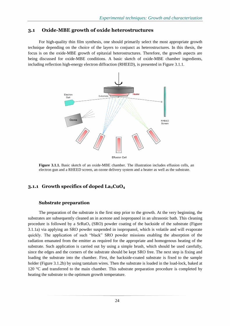
Citation preview

Atomic-Scale Control and Characterization
of Oxide Heterostructures: Correlating
Interfacial Structure and Novel
Functionalities
Max Planck Institute for Solid State Research
by
Y. EREN SUYOLCU
Approved dissertation to obtain the academic degree of Doctor of Natural Science
Technical University of Darmstadt (TUD) – D17
Darmstadt, 2018

This page intentionally left blank

Atomic-Scale Control and Characterization
of Oxide Heterostructures: Correlating
Interfacial Structure and Novel
Functionalities
Dissertation submitted to the Department of Materials and Earth Sciences at
Technische Universität Darmstadt
in Fulfillment of the Requirements for the Degree of
Doctor of Natural Science (Dr. rer. nat.)
by
YUSUF EREN SUYOLCU
from Izmir, Turkey
Referee: Prof. Dr. Peter A. van Aken
Co-referee: Prof. Dr. Hans-Joachim Kleebe
Date of Submission: 13.11.2018
Date of Oral Examination: 17.12.2018
Darmstadt, 2018

Suyolcu, Yusuf Eren: Atomic-Scale Control and Characterization of Oxide Heterostructures:
Correlating Interfacial Structure and Novel Functionalities
Darmstadt, Technische Universität Darmstadt
Publication Year of Dissertation at TUprints: 2019
URN: urn:nbn:de:tuda-tuprints- 89880
Date of Oral Examination: 17.12.2018
Publication under CC BY-SA 4.0 International
https://creativecommons.org/licences/
THESIS SUPERVISORS
Prof. Dr. Peter A. van Aken
Professor of Geo-Material Science
Max Planck Institute for Solid State Research
Stuttgart Center for Electron Microscopy (StEM)
Prof. Dr. Hans-Joachim Kleebe
Professor of Geo-Material Science
Geo- and Material Sciences Department
Technical University of Darmstadt
THESIS COMMITTEE
Prof. Dr. Peter A. van Aken
Referee
Professor of Geo-Material Science
Geo- and Material Sciences Department
Technical University of Darmstadt
Prof. Dr. Hans-Joachim Kleebe
Co-referee
Professor of Geo-Material Science
Geo- and Material Sciences Department
Technical University of Darmstadt
Prof. Dr. Lambert Alff
Examiner
Professor of Materials Science
Materials Science Department
Technical University of Darmstadt
Prof. Dr. Christoph T. Koch
Examiner
Professor of Physics
Physics Department
Humboldt University of Berlin

This page intentionally left blank

To my family…

This page intentionally left blank

Introduction
i
Contents
Abstract ........................................................................................................................ iii
Zusammenfassung ........................................................................................................ v
Acknowledgements ....................................................................................................vii
1. Introduction ..................................................................................... 1
1.1 Motivation ................................................................................................................. 2
1.2 Frame of the thesis ..................................................................................................... 3
2. Background: Functional oxide heterostructures ............................... 5
2.1 Complex perovskite oxides ....................................................................................... 6
2.1.1 The perovskite structures .............................................................................. 6
2.1.2 Crystal-field splitting .................................................................................... 8
2.1.3 Jahn–Teller effect ......................................................................................... 9
2.2 Lanthanum cuprates ................................................................................................. 11
2.2.1 Structure of La2CuO4-based thin films ....................................................... 11
2.2.2 High-temperature interface superconductivity in La2CuO4 ........................ 11
2.3 Lanthanum nickelates .............................................................................................. 14
2.4 Lanthanum manganites ............................................................................................ 15
2.5 Defect chemistry approach ...................................................................................... 16
2.6 Thin film growth: Introduction and main principles ............................................... 19
3. Experimental techniques: Growth and characterization ................. 23
3.1 Oxide-MBE growth of oxide heterostructures ........................................................ 24
3.1.1 Growth specifics of doped La2CuO4 ........................................................... 24
3.1.2 In–situ monitoring: Reflection high-energy electron diffraction ................ 26
3.2 Thin film characterization ....................................................................................... 31
3.2.1 Atomic force microscopy ............................................................................ 31
3.2.2 X-ray diffraction ......................................................................................... 31
3.2.3 Electrical conductivity ................................................................................ 32
3.3 Scanning Transmission Electron Microscopy ......................................................... 33
3.3.1 Specimen preparation ................................................................................. 34
3.3.2 Aberration correction .................................................................................. 35
3.3.3 Imaging techniques ..................................................................................... 36
3.3.4 Spectroscopy ............................................................................................... 38

Introduction
ii
3.3.5 Data analysis ............................................................................................... 40
4. Cuprate-based heterostructures ..................................................... 43
4.1 High-temperature superconducting La2CuO4 bilayers ............................................ 44
4.1.1 Dopant size effects on interface functionalities .......................................... 44
4.1.2 Visualizing Jahn–Teller and anti-Jahn–Teller distortions .......................... 57
4.2 δ-doped high-temperature superconducting La2CuO4 interfaces ............................. 68
4.2.1 Effects of dopant size and valance on cationic distribution ........................ 69
4.2.2 On the effect of growth temperature and tensile strain ............................... 73
5. Cuprate-nickelate heterostructures ................................................ 79
5.1 High-temperature superconductivity at La2CuO4/La2-xSrxNiO4 interfaces ............. 80
5.2 High-temperature thermoelectricity at La2CuO4/LaNiO3 heterostructures ............. 91
6. Cuprate-manganite heterostructures ............................................. 97
6.1 Anomalous Sr distribution at La2CuO4/LaMnO3 heterostructures .......................... 98
7. Nickelate-based oxide heterostructures ........................................ 105
7.1 Structural reconstruction in NdNiO3 thin films ..................................................... 106
8. Epilogue ........................................................................................ 115
9. Appendices .................................................................................... 119
9.1 A : List of publications .......................................................................................... 119
9.2 B : Biographical note ............................................................................................. 120
9.3 C : Honors & awards ............................................................................................. 121
List of Figures .................................................................................... 122
Symbols and abbreviations ................................................................. 130
Bibliography ...................................................................................... 133

Introduction
iii
Abstract
Complex oxide materials providing numerous physical properties can be fabricated in different
forms, for instance in thin films or heterostructures, due to their highly adaptable crystal structures. In
the last decade, the heterostructures of complex oxides have been in high-demand due to their large
number of impressive functionalities, which do not exist in their bulk forms but emerge at the
interfaces. Recent technical improvements of epitaxial growth techniques enable fabricating high-
quality oxide heterostructures, where the phenomena occurring at their interfaces can be tailored
depending on the choice of the constituents. However, the key factor dominating the interface
functionalities is the control of the interface sharpness.
Prominent combination of state-of-the-art atomic-layer-by-layer molecular beam epitaxy (ALL
oxide-MBE) and aberration-corrected scanning transmission electron microscopy (STEM) is utilized
in the thesis, for the atomic-layer-precise synthesis and atomic-resolution characterization of the
heterostructures, respectively. Atomically-resolved STEM imaging [i.e. high-angle annular dark-field
(HAADF), annular bright field (ABF)] and spectroscopy [i.e. electron energy loss spectroscopy
(EELS) and energy dispersive X-ray spectroscopy (EDXS)] techniques are combined with dedicated
conductivity measurements as well as atomic force microscopy and X-ray diffraction. Using these
results, the local structure, octahedral distortions, and chemical properties are correlated with the
functionalities of the systems. For the STEM data analysis, “Oxygen-octahedra picker tool” and
“STEM-SI Warp” software tools are used in order to quantify and to post-correct the (spectrum)
images, respectively.
Complex functional oxide heterostructures consisting of iso-structural or hetero-structural
contacts – mainly based on La2CuO4 and its derivatives – are concerned with the aim of not only
tailoring the novel interface properties, which are directly linked to the local structural and chemical
properties but also identifying the interface sharpness.
First, La1.6A0.4CuO4 / La2CuO4 bilayers composed of a metallic (M) and an insulating phase (I),
where A represents a divalent dopant (namely, Ba2+
, Sr2+
, and Ca2+
), are studied. After the growth
optimization, detailed characterization of the structures – especially extensive STEM investigations –
substantiated the importance of the elemental distribution at the interfaces: Despite the perfect
epitaxial growth, the dopants were found to be inhomogeneously distributed depending on the dopant
size. This distribution defines whether the final superconducting properties emerge due to the striking
“interface effect” or due to “classical” homogeneous doping. Moreover, a clear correlation between
dopant size, dopant distribution and local lattice deformations is underlined suggesting a relationship
between the nature of superconductivity (interface vs bulk) and Jahn–Teller distortions of the anionic
sublattice.
The second example of homoepitaxial (i.e. iso-structural) systems considered in this work is
two-dimensionally-doped (i.e. δ-doped) La2CuO4 superlattices, where specified La–O atomic layers in
the La2CuO4 crystal structure are substituted with A–O layers, in which A is an acceptor dopant (A =
Ba2+
, Sr2+
, Ca2+
). STEM-EELS analyses substantiated that despite the differences on the cation
redistribution lengths, δ-doping results in asymmetric dopant distribution profiles at the interfaces.
Such distribution is correlated with a qualitative model based on thermodynamic considerations and
growth kinetics: As far as the dopant redistribution mechanism is concerned, the main factor leading
to intermixing in the substrate direction is thermal diffusion. On the other hand, the wider distribution
in growth direction is a consequence of the high lateral mobility of the atoms, which triggers the

Introduction
iv
tendency to cationic intermixing at the surface. Moreover, the substrate temperature variation also
affects the cationic distribution length, while the tensile strain induced by the substrate may influence
the asymmetric profile.
Furthermore, the contacts of different materials, namely, lanthanum cuprate and lanthanum
nickelate systems, are studied. High-temperature superconductivity at the interface of lanthanum
cuprate (La2CuO4, 214-phase) and strontium (Sr)-doped lanthanum nickelate (La2-xSrxNiO4, 214-
phase) heterostructures, and high-temperature thermoelectricity of lanthanum cuprate (La2CuO4, 214-
phase) and lanthanum nickelate (LaNiO3, 113-phase) heterostructures are reported. For the former,
i.e. La2CuO4/La2–xSrxNiO4 contacts, the ability to tune the superconducting properties simply by
changing the structural parameters is presented. More importantly, STEM techniques combined with
dedicated conductivity measurements evidenced the decoupling between the electronic charge carrier
and the cation (Sr) concentration profiles at the interface, which induces the formation of a hole
accumulation layer dictating the final superconducting properties. This phenomenon is rationalized in
the light of a generalized space-charge theory. As far as the La2CuO4/LaNiO3 heterostructures are
concerned, the variation of the individual layer thicknesses (with constant total film thickness)
influences the physical properties: As the thickness of the individual layers is reduced, the electrical
conductivity decreases and the sign of Seebeck coefficient changes.
Independent from the functionalities, the differences in chemical sharpness of lanthanum
cuprate–lanthanum nickelate interfaces are further realized, although all the interfaces are structurally
sharp: In the case of La2CuO4/La2– La2CuO4, 214-phase xSrxNiO4/La2CuO4 contacts, the La2CuO4–
La2–xSrxNiO4 interface is sharper concerning the elemental intermixing, while the La2–xSrxNiO4–
La2CuO4 interfaces exhibit a wider Sr distribution. On the other hand, the decrease of individual layer
thickness in La2CuO4/LaNiO3 multilayers results in strong intermixing while thicker cuprate–
nickelate layers maintain sharper interfaces.
In the case of hetero-structural epitaxy of different materials (phases), e.g. superconducting–
ferromagnetic La2CuO4/LaMnO3 multilayers, substantial differences in cationic redistribution and the
local octahedral network is observed. STEM investigations demonstrate that Sr redistribution in 113-
LaMnO3 and 214-La2CuO4 phases is different and this directly affects the sharpness of the interfaces.
In particular, a stronger tendency of Sr segregation (in growth direction) in the 113-phase compared
to the 214-phase is unveiled.
Moreover, detailed high-resolution STEM imaging and spectroscopy of PLD-grown NdNiO3
epitaxial layers on [011]-oriented NdGaO3 substrate experimentally show a structural re-orientation
from the [011]-phase (α-phase) to the [101]-phase (β-phase), which could be understood within the
framework of DFT+U calculations. The calculations further unveil enhanced NiO6 octahedral
breathing distortions for tensile strained α- and β-phases of NdNiO3.

Introduction
v
Zusammenfassung
Aufgrund ihrer flexiblen Kristallstrukturen können mit komplexen Oxiden Dünnschichten und
Heterostrukturen mit sehr variablen physikalischen Eigenschaften, welche im Volumenmaterial nicht
vorkommen, hergestellt werden. Dies hat im vergangenen Jahrzehnt zu einer beträchtlichen
Forschungsaktivität geführt. Aufgrund technischer Entwicklungen können solche Oxid-
Heterostrukturen inzwischen mit hoher Perfektion hergestellt werden. Dadurch wird es möglich, die
Phänomene an den Grenzflächen gezielt zu kontrollieren. Hierbei kommt der Grenzflächenschärfe
eine besondere Bedeutung zu.
In dieser Arbeit erfolgt die präzise Synthese mittels “atomic-layer-by-layer molecular beam
epitaxy” (ALL oxide-MBE). Zur Analyse der Schichten kommt die aberrationskorrigierte Raster
(“Scanning”)-Transmissionselektronenmikroskopie (STEM) zum Einsatz. Diese erlaubt die
Charakterisierung der Proben mit atomarer Auflösung. Für die Abbildung wird die “high-angle
annular dark-field” (HAADF)-Technik sowie die “annular bright-field” (ABF)-Methode angewandt.
Für die chemische Analyse kommen die Elektronen-Energieverlustspektroskopie (EELS) sowie die
energiedispersive Röntgenanalyse (EDXS) zum Einsatz. Diese Messungen werden ergänzt durch
Leitfähigkeitsmessungen, Röntgendiffraktometrie sowie Raster-Kraftmikroskopie. Mit all diesen
Ergebnissen kann somit eine Korrelation zwischen der lokalen Struktur und Chemie und den
funktionalen Eigenschaften der Systeme erarbeitet werden. Für die exakte Bestimmung der Geometrie
der Metall-Sauerstoff-Oktaeder wurden die Programme “Oxygen-octahedra picker tool” und “STEM-
SI Warp” verwendet. Die Messungen erfolgten an verschiedenen Systemen die im Folgenden
beschrieben werden.
(i) Das La1.6A0.4CuO4/La2CuO4-Schichtsystem, wobei La1.6A0.4CuO4 metallisch ist und La2CuO4
ein Isolator. “A” steht für eines der divalenten Dotieratome Ba2+
, Sr2+
und Ca2+
. Nach Optimierung
der Wachstumsbedingungen zeigten die STEM-Resultate die Wichtigkeit der Elementverteilung an
der Grenzfläche auf. Denn trotz perfekten epitaktischen Wachstums zeigten die Dotieratome eine
inhomogene Verteilung. Diese Verteilung bestimmt, ob die Schichten Grenzflächen-Supraleitung
oder Volumen-Supraleitung zeigen. Es konnte eine eindeutige Korrelation zwischen Größe des
Dotieratoms, der Verteilung der Dotieratome und der Geometrie der Metall-Sauerstoff-Oktaeder
festgestellt werden. Dies deutet auf einen engen Zusammenhang zwischen dem Mechanismus der
Supraleitung und Jahn–Teller-Verformung der Oktaeder hin.
(ii) In zweidimensional dotiertem La2CuO4 wurden einzelne La–O-Atomlagen durch A–O-
Atomlagen ersetzt, wobei “A” wiederum für eines der Ionen Ba2+
, Sr2+
, Ca2+
steht. Mit Hilfe von
STEM-EELS konnte gezeigt werden, dass die Dotierprofile asymmetrisch verbreitert sind. Dies wird
mit einem qualitativen thermodynamischen Modell der Wachstumskinetik beschrieben: Entgegen der
Wachstumsrichtung führt thermische Diffusion zu einer Umverteilung der Dotieratome, in
Wachstumsrichtung begünstigt die hohe laterale Beweglichkeit der Oberflächenatome eine
Vermischung mit anderen Atomschichten. Darüber hinaus spielt die Substrattemperatur sowie die
durch das Substrat bedingte Zugspannung eine Rolle.
(iii) Es wurden zum einen Grenzflächen zwischen Lanthankuprat (214-Phase) und Sr-dotiertem
Lanthannickelat (La2CuO4/La2–xSrxNiO4) untersucht welche Supraleitung zeigen. Zum anderen
Grenzflächen zwischen Lanthankuprat (214-Phase) und Lanthannickelat (113-Phase)
(La2CuO4/LaNiO3), bei denen Thermoelektrizität nachgewiesen wurde. Für erstere wird gezeigt, dass

Introduction
vi
die Supraleitung durch Änderung der strukturellen Parameter variiert werden kann. Mit der
Kombination aus STEM und Leitfähigkeitsmessungen wird gezeigt, dass elektrische Ladungsträger
von Sr-Dotieratomen entkoppelt auftreten. Dies wird mittels der verallgemeinerten
Raumladungstheorie erklärt. Für letztere wird gezeigt, dass die physikalischen Eigenschaften von der
Dicke der Schichten abhängt: Mit abnehmender Schichtdicke sinkt die elektrische Leitfähigkeit und
der Seebeck-Koeffizienten ändert sein Vorzeichen.
(iv) Trotz struktureller Schärfe sind die Grenzflächen chemisch nicht scharf. So finden wir,
dass im System La2CuO4/La2–xSrxNiO4/La2CuO4 die La2CuO4–La2–xSrxNiO4-Grenzfläche chemisch
schärfer ist als die La2–xSrxNiO4–La2CuO4-Grenzfläche, welche eine verbreiterte Sr-Verteilung zeigt.
Generell führt eine abnehmende Schichtdicke in La2CuO4/LaNiO3-Vielfachschichten zu stärkerer
chemischer Vermischung.
(v) Im Falle der Heteroepitaxie unterschiedlicher Materialien (Phasen), z.B. bei
supraleitend/ferromagnetischen La2CuO4/LaMnO3-Vielfachschichten, finden wir erhebliche
Elementumverteilung und Störungen des Oktaedernetzwerks. Die Sr-Verteilung in 113-LaMnO3 ist
verschieden von der in 214-La2CuO4 was sich direckt auf die Schärfe der Grenzfläche auswirkt.
Insbesondere neigt Sr (in Wachstumsrichtung) zu stärkerer Segregation in der 113-Phase als in der
214-Phase.
(vi) NdNiO3-Schichten, welche mittels PLD epitaktisch auf [011]-orientiertes NdGaO3
aufgewachsen wurden, zeigten eine strukturelle Umorientierung von der [011]-Phase (α-Phase) zur
[101]-Phase (β-Phase). Das Auftreten der Umorientierung konnte mittels DFT+U Rechnungen
verstanden werden. Die Rechnungen zeigten außerdem, dass die Gitterverzerrung der Atmungsmode
der NiO6- Oktaeder, in unter Zugspannung stehenden α- und β-Phasen von NdNiO3, verstärkt auftritt.

Introduction
vii
Acknowledgements
At the beginning, I would like to acknowledge many people, who supported me and my
research and made this work possible…
First and foremost, I would like to express my gratitude to my supervisor Prof. Dr. Peter A. van
Aken not only for his valuable support but also for giving me the opportunity to conduct my research
at the Stuttgart Center for Electron Microscopy (StEM) at the Max Planck Institute for Solid State
Research. He has always inspired me and guided me to pursue my ideas with great freedom. I would
sincerely like to thank Prof. Dr. Hans-Joachim Kleebe for accepting me as a PhD student at the
Technical University of Darmstadt and for his helpful guidance. Moreover, I would like to thank Prof.
Dr. Lambert Alff and Prof. Dr. Christoph T. Koch for taking place in my thesis committee and for
reading my thesis.
Secondly, I highly appreciate the noteworthy support of Dr. Gennady Logvenov: In addition to
his guidance in thin film growth, it was always instructive to discuss superconductivity and
magnetism with him. Although he was exposed to my crazy ideas – every time I popped up with
another one in his office – he always welcomed me. I also gratefully acknowledge Dr. Yi Wang’s
valuable support in STEM imaging and analyses: I am thankful to both of you for your
encouragement. I would like to especially thank Dr. Wilfried Sigle for the fruitful scientific
discussions from the beginning and also for reading my thesis and giving valuable feedback.
It also has been my privilege to work with many prestigious scientists: I sincerely thank Prof.
Dr. Joachim Maier, Prof. Dr. Bernhard Keimer, and Dr. Eva Benckiser for their great collaborations
and valuable contributions to the projects. I would also like to thank and sincerely acknowledge Dr.
Federico Baiutti, Dr. Matthias Hepting and Gideok Kim for the great team-play, for their worthful
collaboration and friendship.
Many thanks to the people for their contribution in providing a good experimental atmosphere:
Ute Salzberger and Marion Kelsch are gratefully acknowledged due to their guidance in TEM
specimen preparation. Kersten Hahn and Peter Kopold in StEM group and Peter Specht in Thin Film
Technology group are thanked for maintaining all the microscopes and the MBE system in good and
stable conditions. Herewith, a special note to Georg Cristiani: I sincerely appreciate your assistance
during the growths and I will not forget your comments on the RHEED patterns and “photography”.
I thank Dr. Zhicheng Zhong and Dr. Philipp Hansmann for the first-principles calculations on
NdNiO3 project, Dr. Giuliano Gregori for the discussions in the La2CuO4-based projects, Dr. Ionela
Vrejoiu for providing the manganite-ruthenate superlattice samples.
Friends are of always great importance for the difficult periods during the PhD life… First,
special thanks to Dr. Pinar Kaya for the priceless support since 2011 and also many thanks to Dr.
Kahraman Keskinbora, Dr. Yigit Mahsereci, Dr. Filip Podjaski, Pascal Wittclich, Dr. Umut T. Sanli,
Dr. Cigdem Ozsoy-Keskinbora, Dr. Ekin Simsek-Sanli, Alp Can Karacakol, Dr. Werner Dobrautz,
Dr. Matteo Minola, Dr. Alessandro Senocrate, Dr. Luzia Germann, Daniel Putzky, Julia Kröger,
Katrin Fürsich, Dr. Christopher Dietl and Dr. Vesna Srot. I also want to thank whole StEM group for
the nice atmosphere and also the Thin Film Technology group for nicely welcoming me. Of course,
Caroline Heer is not forgotten! Thank you very much for your kind, friendly and valuable support.
Hereby, I would like to acknowledge the Max Planck Society for the Max Planck Society
doctoral scholarship during my PhD.

Introduction
viii
Last but not least, I would like to thank my family for supporting me in all circumstances.
Despite the 2000 kilometers distance, my father was always behind me, my mother was always with
me and my sister was always close to me. Without them and their priceless support without expecting
anything in return, I would not have had the opportunity to perform this study. So glad to have you…
Y. Eren Suyolcu
Stuttgart, 2018

Introduction
1
1. Introduction
Abstract
This chapter comprises the motivation and the framework of the thesis together
with giving a brief summary of the contents to the reader.

Introduction
2
1.1 Motivation
Nowadays, the interest in semiconductor technology and semiconductor interfaces extenuates
due to inherent limitations. Transition metal oxide heterostructures, as being another extensive
materials family, form a multi-directional platform for the emergence of novel properties. [1,2]
Bringing dissimilar constituents together in multilayer systems yields novel phenomena at the
interfaces [3,4], which are normally absent in the constituent materials alone, such as metal-insulator
transitions [5], orbital reconstructions [6], colossal magnetoresistance [7,8] high-temperature interface
superconductivity (HT-IS) [9,10], ferromagnetism [11], formation of 2D electron gas [12],
thermoelectricity [13] etc.. The use of oxide heterostructures – for instance superconducting systems –
in technological applications is still partially hindered due to the lack of fundamental understanding of
structural and chemical properties on the atomic scale. The phenomena occurring at oxide
heterostructure interfaces can be tailored depending on the choice of the constituents; however, the
key factor dominating the interface functionalities is the control of the interface sharpness and/or the
interfacial intermixing.
Recently, the stupendous technical improvements in the synthesis of epitaxial oxide
heterostructures with atomic layer precision, e.g. atomic-layer-by-layer molecular beam epitaxy (ALL
oxide-MBE), have paved the way for fabricating stoichiometric systems and tuning their
functionalities. [14,15] In addition to fabricating such valuable heterostructures, examining the
interfacial structure and chemistry is of vital importance for correlating with the physical properties.
Here, aberration-corrected scanning transmission electron microscopy (STEM) techniques provide a
rich platform for position-sensitive probing of the interfaces with atomic resolution. The unique
combination of two high-end techniques, i.e. ALL oxide-MBE and aberration-corrected STEM, is
ideal for customizing and engineering the interfaces: While ALL oxide-MBE offers precise control of
the heterostructures and the interfaces, STEM techniques provide not only information on the
interfacial structure and chemistry but also allow the quantification of octahedral distortions at the
interfaces, which mediate the properties. [16]
In this thesis, optimization of atomic layer-by-layer growth and/or atomic-resolution
characterization of various complex functional oxide heterostructures – mainly La2CuO4 based
systems in the form of either iso-structural or hetero-structural multilayers – is considered. In
particular, different interfaces and their structural and chemical sharpness are correlated with the
physical properties. The thesis aims at a better understanding of the complex oxide heterostructure
interfaces.

Introduction
3
1.2 Frame of the thesis
The thesis is composed of eight chapters – with individual “Introduction” and “Conclusion”
sections– devoted to different oxide heterostructures and related interface examinations. The summary
of the organization is the following:
Chapter 2: Background: Functional oxide heterostructures This chapter presents a
background to the functional complex oxide systems and properties studied in the thesis.
Chapter 3: Experimental techniques: Growth and Characterization This chapter includes
brief explanations of the experimental techniques conducted in the work such as (i) epitaxial growth,
(ii) thin film characterization, and (iii) atomically-resolved aberration-corrected scanning transmission
electron microscopy.
Chapter 4: Cuprate-based heterostructures In this chapter, high-temperature interface
superconductivity (HT-IS) of La2CuO4-based heterostructures are presented. The fabrication and
detailed characterization – including comprehensive STEM investigations – of bilayer systems, and
the asymmetric dopant distribution profiles linked with growth kinetics at δ-doped superlattices,
which are also correlated with electrical properties, are discussed.
Chapter 5: Cuprate-nickelate heterostructures This chapter discusses cuprate-nickelate
multilayers, where the nickelate layers are employed as 214- and 113-phases for studying ‘high-
temperature superconductivity’ and ‘high-temperature thermoelectricity’, respectively. The former, in
which the presence of space-charge induced HT-IS is revealed, comprises not only the interface
characterization but also the fabrication of the recent samples. For the latter, I focus on STEM
investigations indicating the effect of individual layer thickness on the structural quality.
Chapter 6: Cuprate-manganite heterostructures In this chapter, superconducting-
ferromagnetic heterointerfaces of La2CuO4-LaMnO3 multilayers are presented. The realization of the
structural quality and the elemental identification, as well as the octahedral distortions at the
interfaces, is considered via STEM techniques.
Chapter 7: Nickelate-based heterostructures The chapter focuses on the NdNiO3 thin films
grown on NdGaO3 substrates by pulsed laser deposition. The realization of a structural reconstruction
in the NdNiO3 thin films is demonstrated, and the mechanism behind the reconstruction is rationalized
by DFT+U calculations.
Chapter 8: Epilogue The chapter summarizes the outcome and concluding remarks of the
work.

Introduction
4
This page intentionally left blank

Background: Functional oxide heterostructures
5
2. Background: Functional
oxide heterostructures
Abstract
This chapter gives a brief introduction to perovskite systems and presents a
background of functional oxide heterostructures studied within the scope of the thesis.
The structures and the main functionalities of the heterostructures including cuprate-,
nickelate- and manganite-based systems are summarized. Furthermore, an
introduction to the defect chemistry of related systems and thin film growth principles
are presented.

Background: Functional oxide heterostructures
6
2.1 Complex perovskite oxides
2.1.1 The perovskite structures
The ideal form of a “perovskite” oxide structure is formulated as ABO3, which is composed of
corner-sharing BO6 octahedrons and A-site cations surrounded by twelve oxygen anions. The
oxidation state of the A-sites occupied by a cation determines the electron count on the B-site
transition metal and the valence of A and B cations give rise to the classification of ABO3 perovskites
into three groups: (i) A3+
B3+
O3 (e.g. LaMnO3), (ii) A2+
B4+
O3 (e.g. SrMnO3) and (iii)A1+
B5+
O3 (e.g.
KNbO3). Perovskite oxides span a wide range of crystal structures including basic cubic structures or
complex Ruddlesden-popper phases and different compounds can be derived starting from the highly
adaptable and stable ABO3 perovskites, either via varying the A- and B-site cations or via doping the
system, i.e. via employing substitution of the cations with the dopants. Hence, the ability to tailor the
structures with a variation of A- and B-site cations’ size and/or valence sets the stage for tuning the
functionalities.
The highly adaptable crystal structure of perovskite oxides, not only provides the opportunity
of synthesizing them in different forms, such as ultrathin films and/or heterostructures, but also leads
to various functionalities including ionic conductivity [17], piezoelectricity [18], ferromagnetism [11]
etc. owing to sharing similar lattice parameters and structures, and thereby they can be easily
integrated into each other. In such perovskite oxides, the bonding between B-cation and the O-anion,
which are determined by the size of A and B cations, and correspondingly the B–O–B angle as well as
the B–O bond lengths, play an important role. Relatedly, depending on cation sizes, the BO6
octahedra are modified and the functional properties are tailored in a way that properties can be read
via the interpretation of the octahedral distortions. To distinguish the origin of the distortions of the
ideal structure, one can use the relative differences of the ionic radii of the constituent cations.
Therefore, in order to determine the extent and structural origin of the octahedral distortions in basic
ABO3 structures, Goldschmidt’s tolerance factor (t), which is defined in terms of ionic radii of the
cations and anion, has been used. [19] The tolerance factor is defined as:
𝑡 =𝑅A+𝑅O
√2 (𝑅B+𝑅O) (2.1)
where RA, RO, and RB refer to the ionic radii for the A cation, oxygen (O) and B cation, respectively.
The ideal cubic structure is represented by t = 1. In particular, although being modified by
various distortions – in the cases of t ≠ 1 – the stable ABO3-structure is maintained for 0.8 ≤ t ≤ 1.0.
These octahedral deformations result in different crystal structures with lowered crystal symmetries
and can be mainly exemplified as orthorhombic, monoclinic, rhombohedral and tetragonal structures.
Background: Functional oxide heterostructures
7
Ruddlesden–Popper phases
In addition to the high structural adaptability of perovskites, another important feature is their
easily modifiable stoichiometry, which enables different phases depending on the oxygen content or
the substitution of the A cation by other cations with different valence state. Similarly, Ruddlesden-
Popper (R–P) phases, which are derivatives of ideal perovskites, also exhibit structural and
stoichiometric adaptability, independent of the compound.
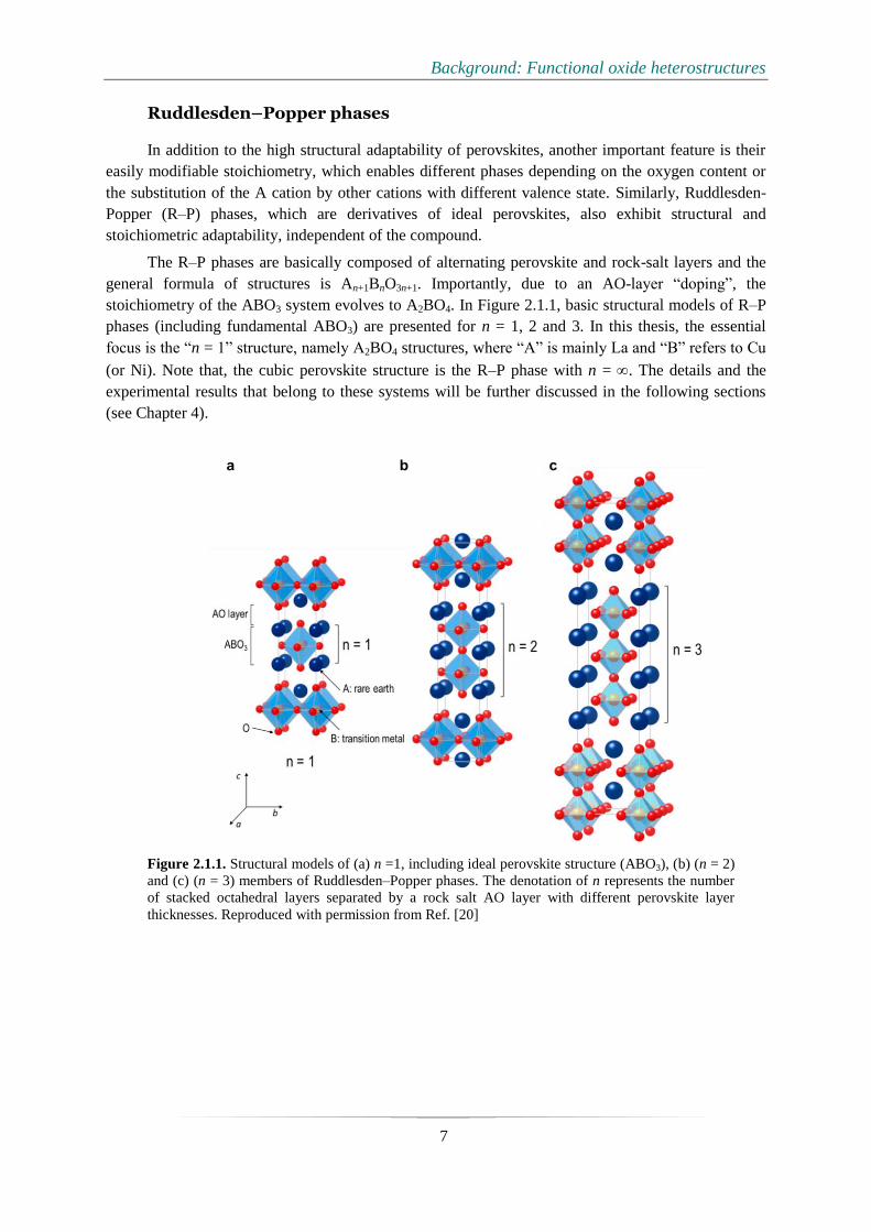
The R–P phases are basically composed of alternating perovskite and rock-salt layers and the
general formula of structures is An+1BnO3n+1. Importantly, due to an AO-layer “doping”, the
stoichiometry of the ABO3 system evolves to A2BO4. In Figure 2.1.1, basic structural models of R–P
phases (including fundamental ABO3) are presented for n = 1, 2 and 3. In this thesis, the essential
focus is the “n = 1” structure, namely A2BO4 structures, where “A” is mainly La and “B” refers to Cu
(or Ni). Note that, the cubic perovskite structure is the R–P phase with n = . The details and the
experimental results that belong to these systems will be further discussed in the following sections
(see Chapter 4).
Figure 2.1.1. Structural models of (a) n =1, including ideal perovskite structure (ABO3), (b) (n = 2)
and (c) (n = 3) members of Ruddlesden–Popper phases. The denotation of n represents the number
of stacked octahedral layers separated by a rock salt AO layer with different perovskite layer
thicknesses. Reproduced with permission from Ref. [20]

Background: Functional oxide heterostructures
8
2.1.2 Crystal-field splitting
In transition metal oxides (TMOs) the electronic transitions and bonding are dominated by
partially or fully filled 3d orbital electrons. When ligands (in our case, oxygen anions; O2-
) are bonded
to the TM ion in an octahedral symmetry, depending on the TM cation and its valence the energy
levels of 3d orbitals are modified. The Crystal Field Theory explains these modifications via the ionic
description of the bonding between TM and O2-
. [21] In these systems, the five-fold degenerate 3d
levels are occupied by electrons that have parallel spins minimizing the Coulomb repulsion according
to Hund’s rule, which briefly states that the d orbitals are filled in a way to lower the energy of the
electrons via maximized spin and angular momentum.
The d orbitals in TMOs (in the present case, mainly, CuO6), are degenerated and due to the
interactions (mainly electrostatic) between the B-3d (e.g. Cu 3d) orbitals and the closest O-2p orbitals,
the degeneracy is broken with the octahedral crystal field effect. In other words, the oxygen anions, as
being negative point charges, have a repulsive effect on 3d orbitals that gets stronger via getting
closer. And, the electron-electron repulsion leads to some differences between the orbitals, i.e. the
destabilization of the system and breaking of the octahedral symmetry. As a result, the energy levels
are linear combinations of high-energy doublet eg (i.e. 𝑑𝑥2−𝑦2 , 𝑑𝑧2) and low-energy triplet t2g (i.e.
𝑑𝑥𝑦, 𝑑𝑦𝑧, 𝑑𝑥𝑧) states (Figure 2.1.2). The energy difference between the eg and t2g states is presented
by crystal-field splitting energy (Δcf), and varies between ~1-2 eV depending on the system and the
extent of the distortion. [22] In the case of electrons occupy t2g orbitals (lower energies), the B cation
gets more stable, whereas in the case of eg orbital occupation at higher energies, the stabilization of
the crystal field is reduced, and the system is less stable. Therefore, the extent of electron transfer in
such systems is determined by the B–O bond length and B–O–B angles (see Section 2.3.2) and hence
the electronic properties are designated within the 3d-orbital electrons of B-site cation and the 2p-
orbitals of the oxygen.
Figure 2.1.2. Illustration of the crystal field effect on d-states of a transition metal cation. The
colored orbital drawings (right) are reproduced from Tokura et al. [22]

Background: Functional oxide heterostructures
9
2.1.3 Jahn–Teller effect
The lowering of crystal symmetries is compensated by modifications of the BO6 octahedron
and these modifications take place in different forms via tilting, rotating, compressing or elongating
the octahedron. In addition to the tilts and rotations of the BO6 octahedra, the lattice symmetry can be
lowered by the Jahn–Teller (JT) effect, which describes that the degenerated electronic states can
accommodate a lowering of their ground-state energy by lifting the degeneracy via a lattice distortion.
[23] In other words, the distortion of the ideal geometry is a consequence of removing the electronic
degeneracy of the highest occupied molecular orbital via energy state splitting and lowering its
symmetry, which provides energy stabilization of the system. [24]
TMOs with BO6 octahedra surrounding the JT transition metal ions such as Mn3+
and Cu2+
,
which have high-spin d4 and d
9 configurations, respectively, exhibit JT distortions, and these
distortions are intimately correlated with the physical properties. [25] For instance, the CuO6
octahedron in the parent La2CuO4 is elongated along the c-axis by the JT effect [26] and exhibits two
long and four short Cu–O bonds. [27]
In an undoped La2CuO4 system, the Cu2+
ion in the CuO6 octahedron is mainly subject to a
crystal field with tetragonal symmetry. As a consequence of that, the five-fold degenerate d-orbitals
of the Cu2+
ion (with 3d9 electron configuration) are split into four energy levels as shown in Figure
2.1.3. The JT distortions are also a subject for LaMnO3-based systems, either in a “cooperative” way
or not. [28] However, the main focus of this thesis is the JT and anti-JT distortions present in the
undoped and doped La2CuO4 systems. For further details see Section 4.2.1.
Figure 2.1.3. Illustration of the crystal-field effect on d-states of a Cu2+
cation with 3d9
configuration. The presentation of the c-axis elongated CuO6 octahedra represents the (enhanced)
JT distortion. [23,29,30]

Background: Functional oxide heterostructures
10
Anti-Jahn–Teller distortion in La2-xSrxCuO4
As mentioned before, in the native lanthanum cuprate, the CuO6 octahedra undergo JT
distortions. However, via hole doping, the structure is contracted and the O–O (or Cu–Oapical)
distances are modified. In order to investigate, whether the JT interaction still plays a role in the local
distortion of the CuO6 octahedra in the presence of hole carriers in ionic crystals such as cuprates,
Shiraishi first performed the total energy band structure calculations of La2−xSrxCuO4 (LSCO) by
varying the Cu–Oapical distance. [31] These calculations have suggested that the Cu-apical-O distance
decreases with increasing the Sr concentration in La2–xSrxCuO4.
After a while, some experimental studies were also conducted in similar systems: Distortions of
CuO6 octahedra in Sr-doped La2–xSrxCuO4 structures (x up to 0.4) and related changes in Cu–O apical
distances were studied via diffraction techniques providing average structural information. [32] It is
reported for this particular system that increasing the dopant concentration determines the
compression of the octahedron (Figure 2.1.4), i.e. a decrease of the Cu–Oapical distances [32], which is
defined as anti-Jahn–Teller (AJT) effect. [26] Recently, the presence of JT and AJT distortions at the
interface of Sr δ-doped layers was reported [33], where an anomalous elongation of the Cu–O apical
distance in LCO-based structures is present, i.e. JT distortion [34] and followed by an AJT distortion
contracting the CuO6 octahedra along the c-axis. Therefore, within the scope of this thesis, the JT and
also anti-JT distortions are widely studied and discussed (see Section 4.2.2), since the local JT
distortions appear to be strongly related to the presence of 2D interfacial superconductivity.
Figure 2.1.4. Illustration of the crystal field effect on d-states of a Cu2+
cation with 3d9
configuration. The c-axis-contracted CuO6 octahedron represents the anti-JT distortion. [26,35]

Background: Functional oxide heterostructures
11
2.2 Lanthanum cuprates
2.2.1 Structure of La2CuO4-based thin films
As briefly mentioned above, La2CuO4 (LCO) is a member of the R–P family with n=1 and
presents the fundamental “214-structure” among the other cuprate-based (superconducting) systems.
The La2CuO4 parent compound is an antiferromagnetic insulator and exhibits an orthorhombic
structure, in which the CuO2 planes are separated by rock-salt La-O blocks. For LCO the A-site is
occupied by nine-fold-coordinated La3+
and the six-fold-coordinated B-site cation, i.e. Cu+2
, is placed
in the center of BO6 octahedra. A sketch presenting the structural model for La2CuO4 is displayed in
Figure 2.2.1.
Figure 2.2.1. Structural model of La2CuO4. La, Cu, and O are colored with green, blue and red,
respectively.
In native LCO, an elongation of CuO6 octahedra has an impact on the c-lattice parameter. [36]
The apical Cu–O (or O–O) bond length is expanded by the Jahn–Teller effect, whereby the system
lowers its energy. As a result, a relatively long c-lattice parameter (~13.15 Å) is achieved compared
with the other compounds, such as isostructural La2CoO4 and La2NiO4 of this family, where the c-axis
lattice parameters are considerably smaller, i.e. ~12.60 Å [37,38] and ~12.70 [39], respectively.
2.2.2 High-temperature interface superconductivity in La2CuO4
The main basis of this thesis is beyond the electronic and theoretical discussions of
superconductors. However, the fundamentals of the structure and the functionalities of cuprate-based
high-temperature superconductor systems will be presented in this section in the form of a compact
summary. The discussions based on the experimental findings are presented in Chapter 4 and 5.
The discovery of the high-temperature superconductivity (HTSC) in cuprates paved the way for
a remarkable extent of interest in the scientific community for decades (Figure 2.2.2a).
Superconductivity in a hole-doped, i.e. Ba-doped, LCO system was first discovered by the
masterpiece of Bednorz and Muller. [40] The main advantage of the proposed system as a ‘high-
temperature superconductor’ is the ability of hole (or electron) doping or oxygen intercalation to the
structure owing to the easily modifiable structure of La2CuO4: The carrier density of the CuO2 layer

Background: Functional oxide heterostructures
12
can be altered due to doping the charge reservoir represented by the La-O blocks, which separate the
CuO2 layers from each other (Figure 2.2.2b), by holes or oxygen interstitials. The main contribution
to superconductivity is provided by the CuO2 planes, not only in the LCO system but also in other
systems such as YBa2Cu3O7, Bi2Sr2CuO6 and HgBa2Cam-1CumO2m+2+δ (Hg-Ba-Cu-O), which show
even higher transition temperatures compared to LCO. For example, the highest Tc (up to ~165 K) in
a cuprate-based superconductor system is the achievement recorded in Hg-Ba-Cu-O. [41–43] As also
mentioned in many earlier studies, any structural disorder and chemical inhomogeneity directly
affects superconducting properties and reduces Tc, therefore fabrication of high-quality structures is of
great significance.
Figure 2.2.2. a) A schematic showing the superconducting transition temperatures of various
classes of superconductors versus the years of each materials’ discovery. b) Layered copper oxides
are composed of CuO2 planes, typically separated by insulating spacer layers. The electronic
structure of these planes primarily involves hybridization of a 3𝑑𝑥2−𝑦2 hole on the copper sites with
planar-coordinated 2px and 2py oxygen orbitals. Reproduced with permission from Keimer et al.
[44]
The superconducting phase is obtained within a certain amount of doping, i.e. 0.06 ≤ x ≤ 0.26
[45–47], while the undoped LCO is an antiferromagnetic insulator and in the overdoped case the
structure shows metallic behavior (Figure. 2.2.3). The hole doping is achieved via substitution of La3+
with a divalent cation (e.g. Sr2+
) or excess oxygen content. The highest Tc is realized in the optimum
doping, i.e. x ~ 0.16. In the cases of Sr, Ba or oxygen doping, one can achieve 40 K, however, via Ca-
doping the highest superconducting transition temperature achieved is around 20 K. Although
numerous studies have been reported on LCO-based superconductor systems, unfortunately, in these
systems the formation of Cooper pairs could not yet be explained with electron–phonon interactions
as suggested in the Bardeen–Cooper–Schrieffer theory [48] for conventional superconductors.

Background: Functional oxide heterostructures
13
Figure 2.2.3. Illustration of a simplified phase diagram of hole-doped La2CuO4 systems. Different
colors mark different phases (AFM, antiferromagnetic; SG, spin glass) and the dashed lines
represent the optimum doping and the related Tc (~40 K for Sr-doping). The diagram is in
agreement with Hashimoto et al. [49] and Keller et al. [50]
Figure 2.2.4. The dependence of resistance on temperature for single-phase and bilayer films. a)
and b) display insulating and metallic single-phase films, respectively. c) includes I-M, M-I and M-
S bilayers with different superconducting transition temperatures, i.e ~15 k, ~30 K and ~50 K,
respectively. Reproduced with permission from Gozar et al. [10]
Background: Functional oxide heterostructures
14
Recently, a milestone in the field of cuprate superconductivity was reached with the study of
Gozar et al. [10], in which they reported the emergence of interfacial superconductivity as a
consequence of adjoining two non-superconducting layers, i.e. one metallic (M) and one insulator (I)
or superconductor (S) (Figure 2.2.4). The interface superconductivity is induced via hole
accumulation and mainly based on charge transfer as a consequence of different chemical potentials
of overdoped and undoped layers in such M–I bilayers. [10] It is also shown that the superconducting
transition temperature depends on the layer sequence, although in all cases HTSC is reached. After
this discovery, one of the principal questions was the following: “How thick is the nominal interface
layer with the highest Tc?”. Logvenov et al. answered this question utilizing “Zinc-doping”
tomography and reported that HT-IS is confined to one “single” CuO2 plane and the “hot”
superconducting plane is the second CuO2 plane after the nominal interface. [51] Later on, Butko et al.
showed that the superconducting Tc is linearly dependent on the c-axis lattice parameter: The larger
the c-lattice parameter, the higher the Tc. [52] A similar relationship between the c-lattice parameter
and Cu–O distances has been also reported. [53,54] Analogue M–I structures were extensively
investigated with the Coherent Bragg Rod Analysis (COBRA) method indicating large changes in Cu-
apical-oxygen distances starting from the nominal M–I interfaces. The results in this thesis leverage
and improve these findings and are presented in Section 4.1.2.
In a recent study, Bauitti et al. showed the contribution of the space-charge region to the HTSC
in δ-doped structures. [55] They have revealed that, in the case of Sr δ-doping, an asymmetric
distribution of the dopant – instead of one individual ML substitution of Sr-O and La-O – results in
the formation of two different interfaces: While one of them provides ionic-intermixing-based
superconductivity through homogenous doping, on the other side of the interface a space-charge layer
is present (see section 4.2). All these studies indicate that the interface control and characterization is
of great significance and LCO-based cuprate superconductors still provide a fruitful ground for
further experiments.
2.3 Lanthanum nickelates
Another example of R–P phases is the Lan+1NinO3n+1 (LNO) family, which has been studied in
the present thesis in two different phases: (i) n = 1 (i.e. Sr:La2NiO4) and (ii) n = ∞ (i.e. LaNiO3). As a
characteristic feature of R–P phases, the properties of different phases remarkably change from one to
another for the Lan+1NinO3n+1 members. For example, the parent compound of the n = 1 phase,
La2NiO4, is an antiferromagnetic insulator while LaNiO3 exhibits paramagnetic metallic behavior.
The synthesis of these two individual structures critically depends on the precise control of the growth
temperature and pressure. For R–P phases with low n-values (e.g. La2NiO4) a less oxidizing
environment (e.g. P ~ 1 x 10⁻⁶
Torr) is favorable. In the case of Sr doping of the compound (i.e. La2–
xSrxNiO4), especially for increasing Sr doping levels, higher oxidizing conditions (e.g. P ~ 2 x 10⁻⁵
Torr) are required. Hole-doping (mainly via Sr) of the parent La2NiO4 is one of the main research
areas of the material system; for instance, La2–xSrxNiO4 thin films with a wide range of doping
concentrations have been extensively studied in terms of insulator-metal transitions or
electrochemical device applications through different synthesis techniques. [56,57] The defect
chemistry of La2–xSrxNiO4 is discussed in Section 2.5.
The 113-phase, i.e. LaNiO3, is the most extensively studied member of the RNiO3 (R = rare
earth ion) family. In general, the family of rare-earth nickelates with composition RNiO3 has recently
Background: Functional oxide heterostructures
15
attracted wide-spread interest following theoretical predictions of possible high-Tc superconductivity.
[58] In more detail, the RNiO3 perovskite structure coordinates the Ni3+
ion to O2-
ions in an
octahedral environment, providing Ni with a 3d7 (t2g
6 eg
1) electronic configuration with one electron in
the eg orbitals. The complex phase diagram of the RNiO3 family mainly stems from emerging
electronic and magnetic correlations as a function of the distortions of the perovskite lattice, with
paramagnetic metallic, paramagnetic insulating, and antiferromagnetic insulating phases arising. [59]
In the bulk form, the LaNiO3 compound exhibits the smallest lattice distortion, and remains metallic
and paramagnetic at all temperatures, while the control of the octahedral network and related Ni–O–
Ni bond-angle distortions in LaNiO3-based heterostructures can induce electronic and magnetic
transitions. [5] The heterostructure environment enables the manipulation of intrinsic interaction
parameters of all RNiO3, which can significantly alter the materials' properties and new phenomena,
can emerge, that are not present in the parent bulk material. In this thesis, LNO-systems (113- or 214-
phases) have been used as complemental-systems to be stacked with La2CuO4-layers. The
experimental findings and discussions can be found in Chapter 5. Moreover, for the lanthanum
cuprate – lanthanum nickelate heterostructures that I contributed to the synthesis, the optimized
growth parameters have benefitted from the previously gained experiences: Further details on the
growth of these systems can be found in Ref. [60,61].
2.4 Lanthanum manganites
Within the scope of this thesis, in addition to cuprate and cuprate-nickelate based
heterostructures, cuprate–manganite (i.e. La2CuO4-LaMnO3) heterostructures with superconducting–
ferromagnetic interfaces have also been studied (Chapter 6). Therefore, I will shortly discuss here the
LMO-based systems and the exchange mechanisms that occur in manganite systems.
The general formula of perovskite manganites is AMnO3 (AMO), where the B-site is occupied
with the transition metal cation “Mn” and the A-site is mainly occupied with rare-earth ions.
Manganate-based complex oxide systems with AMO composition have attracted wide-spread interest
following the variety of magnetic functionalities. [62] In the AMO family, LaMnO3 (LMO) – an
antiferromagnetic Mott insulator – with Mn3+
and t3
2g e1
g occupancy could be named as the major
actor of the playground, which exhibits attractive functionalities based on the profound interplay
between local lattice and magnetic ordering (and also transport properties) that emerge a complex
phase diagram with different physical properties. [63,64] The compounds with Mn4+
and t3
2g e0g
occupancy hindering Jahn–Teller distortions with partially filled 3d shells, in particular, BaMnO3
(BMO), SrMnO3 (SMO) and CaMnO3 (CMO), exhibit different crystal structures. While BaMnO3
favors crystallizing in the more stable hexagonal polymorph, it is less stable in perovskite structure
[65,66]. SMO exhibits both cubic and hexagonal polymorphs [67,68], and CMO shows a distorted
cubic structure. [69]
Exchange interactions in manganites
The complex phase diagram of Sr-doped LMO systems is a consequence of magnetic exchange
interactions, which are superexchange [70,71] and double-exchange interactions mediated by O-2p
orbitals, relying on the orbital degeneracy and occupancy of Mn 3d-orbitals. As mentioned in the
previous section, the main use of doping manganite systems is the modification of the Mn valence in

Background: Functional oxide heterostructures
16
the system. When the Mn3+
ion loses its eg electron, which is the main actor in electrical and magnetic
properties and is loosely bound, the system basically turns to a Mn4+
-bearing structure. This is the
starting point of property-engineering, not only for bulk systems but also, more importantly, for
LMO-based epitaxial heterostructures and interfaces. The exchange interaction between electrons is a
consequence of the electron-electron Coulomb repulsion and Fermi statistics prohibiting the
occupancy of an electronic state by electrons that have identical spins (i.e. two spin-up or two spin-
down). [62] The superexchange interaction is an indirect interaction of two neighboring Mn ions
through the oxygen mediation, where a one-electron-occupied 3d orbital induces the virtual transfer
of two electrons as well as the dispersion of O-2p electrons to unoccupied Mn 3d-orbitals. [71]
Namely, the virtual electron transfer between the TM cations is present, where the electrons are
localized, and an antiferromagnetic interaction emerges. On the other hand, the mixed-valence
manganite (La, A)MnO3 (e.g. A = Ba, Sr, Ca) is a prototypical compound for the double-exchange
interaction, in which an e1
g electron from Mn3+
can hop without energy cost between Mn3+
and Mn4+
with an orbital configuration t3
2g e1
g and t32g e
0g, respectively. [72] In this case, unlike the
superexchange interaction, the electrons are delocalized which mediate the ferromagnetic interaction.
At the end, the spins and the ions are parallel and ferromagnetically aligned, respectively.
2.5 Defect chemistry approach
Defect chemistry of doped La2CuO4
The properties of complex oxides strongly depend on the dopant concentration and oxygen
content, and thereby, the defect chemistry plays an important role in the engineering and manipulation
of their functional properties. [73–75] Hole (ℎ•) doping of a parent LCO via substituting La3+
with
divalent cations, such as Ca2+
, Sr2+
, and Ba2+
, (or via oxygen interstitials (𝑂𝑖′′)) is a common way to
alter the charge carrier concentrations, as explained in previous sections. Depending on the choice of
the dopant, different extent of segregation (see section 4.1.1) or different solubility limits are obtained.
In this thesis, Ca, Sr, and Ba are used as dopants, where the solubility limit of Ca in LCO is the
smallest (x ~ 0.1) and higher solubility limits (x ~ 1.4) for Sr and Ba are present. [76,77] Now, I will
briefly present the hole doping mechanisms in our model material La2CuO4 from the defect chemistry
approach [78], which has been explained by Maier and Pfundtner in detail. [74]
When the native La2CuO4 is subjected to dopant incorporation, e.g. Sr doping on a La site
(𝑆𝑟𝐿𝑎′ ), the increase of holes can be defined by:
2𝑆𝑟𝑂 + 2𝐿𝑎𝐿𝑎𝑥 +
1
2𝑂2 = 𝐿𝑎2𝑂3 + 2𝑆𝑟𝐿𝑎
′ + 2ℎ• (2.2)
In the case of such doping, the formation of oxygen vacancies (𝑉𝑂••) is also expected and can be
defined by the following equation:
2𝑆𝑟𝑂 + 2𝐿𝑎𝐿𝑎𝑥 + 𝑂𝑂
𝑥 = 𝐿𝑎2𝑂3 + 2𝑆𝑟𝐿𝑎′ + 𝑉𝑂
•• (2.3)

Background: Functional oxide heterostructures
17
Moreover, the anti-Frenkel reaction considering an oxygen site (i.e. 𝑂𝑂𝑥) should also be taken
into consideration as:
𝑂𝑂𝑥 + 𝑉𝑖
𝑥 ↔ 𝑂𝑖′′ + 𝑉𝑂
•• (2.4)
As a last step considering the mass-action law, the final electroneutrality condition is defined
as:
2[𝑂𝑖′′] + [𝑆𝑟𝐿𝑎
′ ] + 𝑛 = 𝑝 + 2[𝑉𝑂••] (2.5)
For a more general picture, when Sr-doped LCO is taken as a reference, the solution as a
function of oxygen partial pressure can be simplified as presented in Figure 2.5.1a. For the
intermediate-oxygen-pressure regime (middle), which is the most common case, the extent of hole
doping is constant depending on the extent of the Sr-La substitution. However, in the high-oxygen-
pressure regime (right), the main defects are expected to be the double positively charged oxygen
interstitials and the dopant compensation is negligible. In the case of low oxygen partial pressures
(left), the presence of oxygen vacancies is expected, and the extent of oxygen interstitials is low and
constant.
In some cases, the dopant concentration may not be constant in the doped regions of epitaxial
LCO systems, for instance at the interfaces, depending on the cationic intermixing. [79] Therefore,
one should also consider the defect concentrations as a function of Sr-doping (Figure 2.5.1b). For this
case, I take Sr-doping as a reference and refer to the study of Maier et al. [74] again. From the defect
concentration model, it is visible, that at a fixed Sr-doping concentration for the low-doping case, the
extent of oxygen interstitials accompanies the extent of Sr-doping. However, when the Sr content
increase, the oxygen interstitials starts to dwindle away, and the hole formation increases in this case.
Besides, very high doping of Sr results in the generation of defect associates, either neutral or not, are
expected, e.g. {2(SrLa)VO}.
The prediction of defect concentration in doped LCO systems is crucial since the defects
directly influence structural properties that have further effects on superconducting properties.
Previous reports already showed that while oxygen vacancies contract the structure, Sr-doping and/or
oxygen intercalation expands the unit cell along the c-axis. [73,75,76,80] See Sections 2.1.3 and 4.2.2
for further literature and experimental findings, respectively.

Background: Functional oxide heterostructures
18
Figure 2.5.1. a) Defect concentration in La2CuO4 as a function of oxygen partial pressure at given
Sr-content and constant temperature. b) Modeled defect concentration in La2CuO4 as a function of
Sr-doping at constant temperature and oxygen partial pressure. Reproduced with permission from
Maier et al. [74]
Defect chemistry of doped La2NiO4
Since La2NiO4 (LNO-214) share the same R-P structure with La2CuO4, it can be considered
within similar chemical descriptions as well. Starting from the insulating stoichiometry compounds,
an electronic phase transformation can be achieved by increasing the electron hole concentration. In
particular, for (LNO-214) a transition into a metallic phase with increasing p (up to p ~1.0) has been
observed. [56] Moreover, in (LNO-214), the substitution of La with an acceptor dopant (mostly Sr+2
)
or intercalation of oxygen in the form of interstitial defects, results in hole doping, similar as for LCO.
Both LSNO and LSCO can also accommodate a large amount of double-positively charged oxygen
vacancies, thereby the general electroneutrality condition reads as equation (2.4). [74,81,82] By
considering the above-described chemical models of LCO and of LSNO, a chemical potential
gradient for holes and oxygen vacancies, as well as for Sr, is present, once a contact between these
two compounds is formed. As a consequence, in order to establish equilibrium conditions, migration
of defect species from LSNO in the direction of LCO should take place, [61,83] which in turn is
expected to deeply affect the final functionalities of the interface region. For further details see
Section 4.3.

Background: Functional oxide heterostructures
19
2.6 Thin film growth: Introduction and main principles
The advantage of fabricating thin films and heterostructures of different components serves as a
multifunctional platform leading to novel properties and the ability to create high-quality epitaxial
heterostructures is the starting point of engineering physical properties at interfaces. As is well
established, the precision of the growth techniques is a crucial factor in having an impact on the
properties. Therefore, either physical [e.g. molecular beam epitaxy (MBE), pulsed laser deposition
(PLD)] or chemical [e.g. chemical vapor deposition (CVD), atomic layer deposition (ALD)], different
growth techniques have been developed and used depending on the choice of the material systems and
applications. Some examples of interesting properties can be given as the occurrence of
ferromagnetism at the interface between a paramagnetic (i.e. CaRuO3) and an antiferromagnetic (i.e.
CaMnO3) layer [11] or the emergence of a 2D electron gas at the interface between two band
insulators, namely SrTiO3 and LaAlO3. [12] Moreover, the interfacial superconductivity occurring at
metal-insulator interfaces of La2CuO4-based heterostructures is another significant example, which
constitutes the backbone of this Ph.D. thesis and will be further explained in the following chapters.
Growth modes
Independent of the growth technique, thin film growth modes can be classified as island growth
(i.e. Volmer-Weber mode), layer-by-layer growth (i.e. Frank–van der Merwe mode) and layer plus
island (i.e. Stranski-Krastanov mode) growth. Island growth is a consequence of the strong bonding
between the particles (either atoms or molecules) on the surface of the substrate, and thus results in
the formation of 3D islands and mostly causes inhomogeneous film formation. The second growth
mode, i.e. Frank–van der Merwe mode, provides layer-by-layer growth generating uniform films and
smooth surfaces, in which the deposition of a layer is followed by another layer and (mostly and
preferably) no nucleation or island formation occurs. The third mode, namely layer plus island mode,
is a mixture of two mechanisms in which layer-by-layer growth is followed by island formation. For
instance, a decrease in substrate temperature may cause such a situation, where the more energetic
particles on the surface start to lose their momentum and thereby start to nucleate. In a growth process
at high-temperature, the high-energetic mobile particles (adatoms) on the surface move towards and
stick to surface steps on the substrate, since these positions are thermodynamically favored. This type
of growth is called step-flow growth.
Growth kinetics
The initial parameter affecting growth kinetics is the (substrate) temperature. The interaction
(i.e. heat transfer) between the particles and the substrate may increase the energy of the particles and
thereby contribute to the extent of surface diffusion. The kinetic energy of the particles directed to the
substrate depends on the epitaxial growth technique. In the MBE growth, the thermal evaporation of
the metals is the main activation factor that results in the low kinetic energy of particles around 0.1
eV. This makes a difference compared to other growth techniques. In particular, in PLD systems the
energy of the particles to be deposited on the substrate is two orders of magnitude higher (i.e. ~10 eV)
than in MBE.

Background: Functional oxide heterostructures
20
Another crucial parameter is the gas pressure of the system. The growth of most of the oxide
epitaxial systems is carried out at “high” pressures due to the involved oxidant species, where the high
background pressure may cause a blocking effect for the particles on the way to the substrate. As
mentioned before, the “low”-energy particles approaching the surface may be blocked due to the
background pressure and may not even reach the substrate. For example, in oxide-MBE, where the
ballistic transport of the ingredients from effusion cells is present, the mean free path of the particles
is crucial and the pressure of the system is in the range of around 10-5
Torr that limits the elements to
be deposited (see Section 3.1.2). Therefore, the growth kinetics and their control are the main frames
of the growth success. The effect of the chamber pressure on the elemental choice and its relationship
with RHEED patterns is further explained in Section 3.1.3.
Stoichiometry control is another critical factor, which is not independent of the growth
technique. For instance, although the structural control of the epitaxial layers is easier in MBE-growth
(due to the low growth rates), the control of the stoichiometry is more difficult since the manual
control of every single layer is important. However, oppositely, in PLD growth, where the growth rate
is higher than in MBE, the stoichiometry of the epitaxial film is already defined by the target, but due
to the faster growth, the manual layer-by-layer control is not allowed. In other words, depending on
the needs, every growth technique presents advantages and disadvantages varying on the desired
achievements. For example, the control of the stoichiometry could be defined as a relative weakness
of the oxide-MBE systems, especially compared to PLD systems. While perfect structural coherency
is achieved at the interfaces, chemical intermixing is a matter of fact up to a certain point (~1-2 nm).
[79,84] It has been shown in a recent report that while MBE yields sharper interfaces, the cation
stoichiometry is more difficult to control compared to PLD growth of the same structures. [85]
Choice of substrate
To be able to grow high-quality films one needs to pay attention to the proper substrate
selection first. The substrates determine mainly the expected extent of the defects, e.g. misfit
dislocations or islands in the films. The worth-stressing factor in substrate choice is the lattice-match
between the substrate and the film to be grown. In a heteroepitaxial growth, which is mostly the case
for strain-engineered interfaces [86], the lattice parameter of the substrate (as) is different than the
lattice parameter of the film (af). In a growth with a small lattice mismatch, for instance, the first
layers of the epitaxial film will be strained to provide the lattice match to the substrate. The
magnitude of the induced strain is usually defined by factor (f) and used for revealing the strain to be
either tensile or compressive:
𝑓 =𝑎𝑓−𝑎𝑠
𝑎𝑠 x 100 (2.5)
In this thesis, for the growth of LCO-based heterostructures, I mainly used LaSrAlO4 (LSAO)
(001) substrates since it induces compressive strain to the epitaxial layer and leads to the highest
critical transition temperature (Tc) for LCO systems among other substrates. [87] LSAO has a
tetragonal structure with lattice parameters a = 0.3754 nm and c = 1.2635 nm, while bulk LCO has an
orthorhombic structure where Cu–O planes are separated by two La–O planes. The lattice parameters
of bulk LCO are a = 0.5335 nm, b = 0.5415 nm, and c = 1.3117 nm. [52] Although LCO exhibits an
orthorhombic structure at room temperature in the bulk form, it can be considered as pseudo-
tetragonal: The orthorhombic LCO structure adopts the tetragonal structure of the LSAO substrate,
Background: Functional oxide heterostructures
21
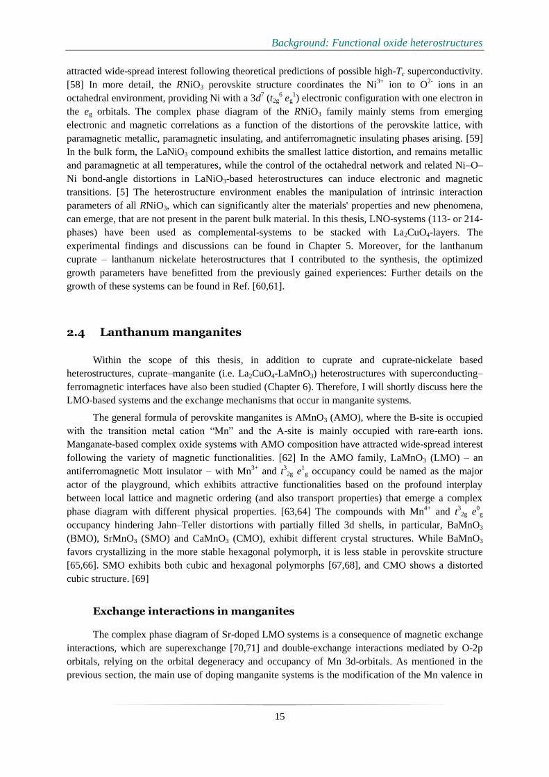
since it maintains an epitaxial relationship with the substrate. [88] An illustration of such situation is
presented in Figure 2.6.1. On the other hand, other substrates, for instance, (LaAlO3)0.3(Sr2TaAlO6)0.7
(LSAT) inducing tensile strain may cause defects in the film as discussed in Section 4.2.2.
Figure 2.6.1. a) Structural models exhibiting the pseudo-tetragonal lattice representation for LCO
(top) and the tetragonal LSAO (bottom). b) STEM-HAADF image representing the tetragonal
(LSAO) and pseudo-tetragonal (LCO) structures on the bottom and on the top part of the image,
respectively. The dashed line indicates the interface. Reproduced from Suyolcu et al. [89]

Background: Functional oxide heterostructures
22
This page intentionally left blank

Experimental techniques: Growth and characterization
23
3. Experimental techniques:
Growth and characterization
Abstract
This chapter aims to give a detailed view of the experimental techniques
employed within the thesis. In particular, the background and practical information
about the growth of La2CuO4-based systems, the thin film characterization and,
comprehensively, aberration-corrected scanning transmission electron microscopy
methods are presented.
Experimental techniques: Growth and characterization
24
3.1 Oxide-MBE growth of oxide heterostructures
For high-quality thin film synthesis, one should primarily select the most appropriate growth
technique depending on the choice of the layers to conjunct as heterostructures. In this thesis, the
focus is on the oxide-MBE growth of epitaxial heterostructures. Therefore, the growth aspects are
being discussed for oxide-MBE conditions. A basic sketch of oxide-MBE chamber ingredients,
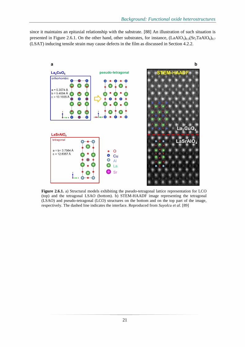
including reflection high-energy electron diffraction (RHEED), is presented in Figure 3.1.1.
Figure 3.1.1. Basic sketch of an oxide-MBE chamber. The illustration includes effusion cells, an
electron gun and a RHEED screen, an ozone delivery system and a heater as well as the substrate.
3.1.1 Growth specifics of doped La2CuO4
Substrate preparation
The preparation of the substrate is the first step prior to the growth. At the very beginning, the
substrates are subsequently cleaned an in acetone and isopropanol in an ultrasonic bath. This cleaning
procedure is followed by a SrRuO3 (SRO) powder coating of the backside of the substrate (Figure
3.1.1a) via applying an SRO powder suspended in isopropanol, which is volatile and will evaporate
quickly. The application of such “black” SRO powder missions enabling the absorption of the
radiation emanated from the emitter as required for the appropriate and homogenous heating of the
substrate. Such application is carried out by using a simple brush, which should be used carefully,
since the edges and the corners of the substrate should be kept SRO free. The next step is fixing and
loading the substrate into the chamber. First, the backside-coated substrate is fixed to the sample
holder (Figure 3.1.2b) by using tantalum wires. Then the substrate is loaded in the load-lock, baked at
120 °C and transferred to the main chamber. This substrate preparation procedure is completed by
heating the substrate to the optimum growth temperature.

Experimental techniques: Growth and characterization
25
Figure 3.1.2. Photographs of (a) the backside SRO coated LSAO substrate and b) the view of the
sample holder after fixing the substrate via tantalum wires.
Growth rate control and ozone production
After the substrate preparation and loading, which is followed by heating, the operator needs to
further control the system and the growth parameters. The growth rate control starts even before the
growth, for which the effusion cells are warmed up to the temperature values providing the
appropriate vapor pressures for the elements that guarantee the desired growth rates. The optimization
of the growth rates at high-oxygen-background rates is of significance on the way to high-quality
growth. This is the reason why, before the growth, for each element (source), the absolute growth
rates are carefully calibrated by utilizing an integrated quartz crystal microbalance (QCM) system in
vacuum. It should be noted here that, the initial calibration to obtain a fudge factor for each element
has been conducted by using ex-situ Rutherford backscattering analyses, which provides the absolute
numbers of deposited atoms and enables the daily use of in-situ QCM. During the calibration of single
sources (elements), certain pauses (~3 min) are applied in between, whereas in the case of consecutive
calibration of the same elements evaporated from different effusion cells (e.g. La) such pauses are not
required, since the stabilization of one cell is conducted, while the other effusion cell (of the same
element) is being calibrated.
In oxide-MBE, the growth rates are ~1 Å/min and in most cases, higher growth rates are not
preferred. The limited heating of the effusion cells restricts the growth rates and thereby limits the
range of the elements to be grown in the system. One would normally expect the control of higher
growth rates in the system. However, due to such limitation, some elements and their oxide
compounds cannot be grown stoichiometrically. One example is the growth of Sr2RuO4 that could be
conducted via PLD, but not with MBE, where the operating temperature of the effusion cells is
limited (~2000 °C).
As is well established, MBE growth is in the ballistic regime and is characterized by long mean
free paths of the initial (elemental) particles during the growth, in which the probability of collision of
the particles is almost zero on the way reaching the substrate. This is also influenced by the pressure
in the chamber. For oxidizing the evaporated elements, the oxidant species must be delivered in the
system; in our system, distilled ozone, is used, which is a production of an ozone generator
(discharger) system, that is stored (in liquid form) in an insulated glass still. The control of ozone
delivery is critical because it is directly related to the pressure of the system and thereby is in a direct

Experimental techniques: Growth and characterization
26
correlation with the mean free path of the particles and the growth rate. It should be noted, that
although the nominal product is ozone (O3), in the end, a small extent of radical oxygen and
molecular oxygen (O2) accompanies the ozone. Furthermore, the system also allows tuning the
delivered gas extent during the growth that enables investigating different conditions (see Section
3.1.3), while the optimum pressure is around 10-6
– 10-5
Torr.
Moreover, in complex oxide-MBE systems having several effusion cells, the optimization and
the stabilization of the element fluxes are of importance. Such stabilization gets more crucial in the
use of different dopants having the same valences, such as Ba, Sr, and Ca, which are widely studied in
this thesis, due to different electron affinities. Therefore, the stabilization of different phases at
different temperatures is required. For instance, in this work, the effusion cell temperatures are
optimized at ~1650 °C, ~500 °C, ~350 °C and ~450 °C, for La, Ba, Sr and Ca, respectively. It should
be noted that the idle temperatures of the effusion cells are different and are still higher than the room
temperature. This is crucial especially for the Cu source, which is kept in a molten state at high
temperatures (~950 °C) even in the idle mode. Because, in the case of cooling down the cell, the
copper transforms into a solid state and cracks the (alumina) crucible, which requires extra
maintenance at the end.
3.1.2 In–situ monitoring: Reflection high-energy electron diffraction
For oxide heterostructures, especially for superconducting systems, the structural quality of the
samples has a direct impact on the properties. Therefore, the precise in-situ monitoring and control of
the growth process are of great significance. In addition to the optimization of the growth parameters,
one needs to take into consideration the instant control of the stoichiometry, and at that point, in-situ
reflection high-energy electron diffraction (RHEED) as a monitoring tool comes to the playground.
The evolution of the RHEED pattern and intensity oscillations provides feedback for precise growth
control. [90–92] More specifically, the RHEED intensity oscillation enables observing the surface
reconstruction, which is the ordered arrangement of the surface atoms and is crucial for understanding
the growth process and the final morphology. [93–95]
In RHEED, an electron beam emanating from the electron gun is reflected from the epitaxial
layers on the surface and results in specular spots (and streaks) on the fluorescent RHEED screen
(Figure 3.1.1). Depending on the surface roughness the reflection varies: The rougher the surface, the
less the intensity of the spots (i.e. diffuse reflection). It should be underlined that owing to the
particle-wave behavior of electrons, both reflection and diffraction occur through the interaction
between the surface atoms and the electron beam. The surface atoms during the growth are mobile
and in order to minimize the surface energy, they change their positions on the surface. As
experimental examples, the specular spot oscillations – recorded during the growth – as a function of
time for a La1.6Ba0.4CuO4/La2CuO4 bilayer are presented in Figure 3.1.3. In these plots, completion of
each La2CuO4 (either doped or undoped) is represented by the maxima of the oscillations. Conversely,
the minima indicate the formation of La–O blocks. Here, for further interpretation of experimental
RHEED patterns, I present a preliminary case study of the surface reconstructions observed during the
MBE growth of L(S)CO-based systems.

Experimental techniques: Growth and characterization
27
Figure 3.1.3. The specular spot (00) (red) and Bragg spot (10) (blue) oscillations are recorded
during the growth of La1.6Ba 0.4CuO4/La2CuO4 bilayer. The intensities were integrated over selected
areas, and one oscillation corresponds to a half u.c. thickness of the La2CuO4-based crystal structure.
The dashed lines indicate the nominal M–I interface.
Surface reconstructions
In a nominal growth of LCO epitaxial thin film on (001) LSAO substrate, first, two La–O
atomic layers are deposited, and this is followed by the deposition of one Cu-O atomic layer in
accordance with the chemical formula of La2CuO4. During the growth, the substrate is heated up to
~650°C in ozone atmosphere with the pressure of ~1.5x10⁻⁵
Torr provided by the evaporation of the
liquid phase. In the case of Sr-doped LCO compounds (i.e. LSCO), a part of La atoms is replaced by
Sr atoms in the co-deposition regime, i.e. simultaneous evaporation of La and Sr atoms are in a
proportion corresponding to a doping level.
Concerning the growth process of optimum doped La1.84Sr0.16CuO4, excluding the first couple
of unit cells, in which the LSCO compound accommodates to the LSAO substrate, a characteristic
surface reconstruction corresponding to a coherent atomic arrangement is obtained. Specifically, after
the deposition of two (LaSr)–O atomic layers, the intensity of the specular spot drops to a minimum
as a consequence of the destructive interference from La2O3 and SrO nano-islands, which cause a
rougher surface, and the additional diffraction streaks disappear. After the Cu shutter is open and Cu
atoms are being deposited on top and the intensity of the specular spot increases. In particular, when
the deposition of half of the Cu–O atomic layer is completed, the characteristic shoulder appears in
the intensity oscillation and two additional diffraction streaks develop between the Bragg diffraction
and the specular spot corresponding to a surface atomic ordering with 3a in-plane width, where a is
the in-plane Cu–O–Cu distance (Figure 3.1.4a). Further deposition of Cu atoms and completing a Cu–
O atomic layer results in an abrupt transformation to 5a pattern (four additional diffraction streaks)
(Figure 3.1.4b). The observation of such typical reconstructions has been an enigma of the high-
quality epitaxial growth of the (La,Sr)2CuO4 compounds for a long time, however, the mechanism
lying behind has not been considered, and thus, not well understood yet.
Experimental techniques: Growth and characterization
28
Figure 3.1.4. RHEED images obtained during the growth of optimum (x =0.16) Sr-doped La2CuO4.
The two additional streaks in (a) and four additional streaks in (b) indicate the “half” and the
“complete” deposition of the Cu–O layer, respectively.
Surface chemistry
Consecutive deposition of the constituent metals on a hot substrate (i.e. ~650° C) in oxidation
conditions enables the fundamental surface chemical reactions. First, neutral nano-sized oxides (i.e.
La2O3 and SrO) are formed following the delivery of La (or La+Sr). After the deposition of the copper
(Cu) metal, one molecular layer of the L(S)CO is formed via the following surface chemical reaction
due to the difference in electronegativities of La/Sr and Cu atoms:
(1 −𝑥
2) × 𝐿𝑎2𝑂3 + 𝑥 × 𝑆𝑟𝑂 + 𝐶𝑢𝑂 → (𝐿𝑎, 𝑆𝑟)2𝐶𝑢𝑂4−𝛿 (3.1.1)
where x is the Sr doping level and δ is the oxygen non-stoichiometry (or concentration of
oxygen vacancies). The entire growth process is a periodic repetition of this reaction. In the 214-
structure formation, two molecular layers form “one” unit cell of a tetragonal LSCO structure (Figure
2.2.1). In other respects, the stoichiometry of LSCO compound (namely the La+Sr to Cu ratio) is also
found to play a role in the determination of the surface reconstruction. At nominal stoichiometry,
(La+Sr)/Cu ratio is equal to 2; however, when the amount of Cu is increased slightly, just before the
nucleation of CuO precipitates, very dense reconstruction lines are visible. Such experimental
observation is used for feedback and for the precise control of the molecular layers’ stoichiometry
during MBE growth of LSCO compounds within the scope of the thesis.
Structural origin
In addition to the previous observations, it is deduced that the lattice mismatch with the
substrate has an impact on the surface atomic arrangement as well. In particular, LSCO grown on
LSAO substrate inducing compressive strain (Figure 2.6.1) causes 5a width atomic arrangement
(Figure 3.1.4b). However, for the growth of LSCO on other substrates, in which the film undergoes
tensile strain, such as STO and LaSrGaO4 (LSGO) 4a pattern (Figure 3.1.5a,b) is observed for the
same doping level. This clearly indicates the influence of strain on the surface atomic arrangement.
Furthermore, in order to examine the dopant size effect on the surface reconstruction, Ca2+
ions,
which have a smaller ionic radii (90 pm) compared to Sr (131 pm) [96], are employed as a dopant for

Experimental techniques: Growth and characterization
29
the growth of LCCO on LSAO substrate and a 4a in-plane atomic arrangement is revealed (Figure
3.1.5c). All these experimental facts substantiate that surface reconstruction is influenced by structural
effects.
Figure 3.1.5. RHEED images obtained during the growth of La1.84Sr0.16CuO4 films grown on (a)
(100) STO and (b) (001) LSGO substrates inducing tensile strain: Three diffraction lines refer to the
4a width (in-plane) atomic ordering for both cases. (c) RHEED image after the deposition of the Cu
layer during the growth of La1.84Ca0.16CuO4 film on LSAO substrate exhibits three diffraction lines
similarly.
Influence of oxygen pressure
Superconducting properties and for higher doping levels, one can even expect the formation of
defect associates, for instance, the formation of oxygen vacancies together with the hole doping.
[74,97] Therefore, considering the significant role of the oxygen and the oxygen vacancies in the
surface reconstruction of LCO-based epitaxial films, further experiments are conducted via
modulating the oxygen pressure. In order to verify the role of ozone assistance, as a first experiment,
after depositing A-site atoms (e.g. La and Sr) under oxidation conditions, we deposit B-site (Cu)
atoms in “vacuum”. In this case, one can still expect the reaction according to equation (3.1.1).
However, the oxygen concentration will be reduced (in a more controlled way) and more oxygen
vacancies will form causing a novel surface reconstruction, correlatively. The second experiment,
which validates the first one, aims to compensate the lack of oxygen in the 214 structure with the
delivery of ozone. The results are presented in Figure 3.1.6. Our experiments reveal that the optimum
doped LSCO films lead to 4a width in-plane surface ordering in vacuum [Figure 3.1.6(a)] (similar to
optimum doped LSCO films grown on STO substrates in ozone), which is consistent with the
expected increase of oxygen vacancy concentration, whereas the visible broadening of the
superstructure streaks in the RHEED image indicates the possible increase of the surface disorder in
vacuum. Importantly, the post-annealing in ozone provides fast (i.e. several seconds) and clear
recovery to the nominal surface ordering [Figure 3.1.6(b)], which strongly evidences the participation

Experimental techniques: Growth and characterization
30
of the oxygen atoms in the healing of the surface imperfections (caused by the oxygen vacancies) as
well as the enhancement of the surface ordering. These observations not only provide additional
information on the surface layer formation during the layer-by-layer MBE growth of LCO-based but
also demonstrate the vital contribution of the oxygen atoms.
Figure 3.1.6. RHEED images of epitaxial La1.84Sr0.16CuO4 films acquired after the Cu layer
deposition in (a) vacuum and (b) after ozone annealing. The oxidation atmosphere causes different
surface reconstructions.
The characteristic 5a0 width (in-plane) atomic ordering can be related to the size of electrostatic
interactions between the dopants and the CuO2 planes and can be correlated with the distribution of Sr
dopants in the optimum doped regimes. Such reconstruction pattern is obtained almost in the entire
doping range from x > 0 to x = 0.2. This is caused by the combination of oxygen interstitials and Sr
dopants during the ozone-assisted growth, where the optimum doping is achieved by such a
combination. In the light of these findings, one can suggest that the two dopants, i.e. created holes and
oxygen interstitials, introduce local crystal distortions, which are directly displayed in RHEED screen
as surface reconstruction. Furthermore, reduced dimensions in the case of vacuum growth – compared
to ozone assisted growth – can be attributed to the formation of oxygen vacancies, where the post-
ozone-annealing heals these oxygen vacancies. In the optimum doping case, a quasi-homogeneous
superconducting ground state is observed. When one moves to the overdoped regime, supercells start
to overlap, and more and more oxygen vacancies are generated to compensate valence dis-balance
resulting from the substitution of La+3
by Sr+2
atoms.
These experimental observations demonstrate that for oxide heterostructures, in particular for
La2CuO4-based HTSC systems, the precise control of the growth process and the stoichiometry can be
monitored via in-situ RHEED in detail. Direct observation of many parameters affecting the surface
reconstructions such as the dopant size, the choice of the substrate (i.e. the strain), the oxygen
pressure and the doping concentration are revealed. Based on these comprehensive experimental
observations, one can further suggest that there is a characteristic size of the surface atomic
arrangements. The presence, the size and the formation of such ordering may have a crucial
implication on the mechanism of HTSC. Further details are in preparation for publication. [98]

Experimental techniques: Growth and characterization
31
3.2 Thin film characterization
3.2.1 Atomic force microscopy
After the growth, one needs to examine the surface quality of the samples. A convenient way to
examine surface morphology is performing atomic force microscopy (AFM) measurements, which
provide valuable information about surface roughness and the presence of any secondary phase
precipitates. AFM is a scanning probe microscopy technique which is based on the electrostatic forces
between the scanning cantilever including a sharp tip and the surface of the sample. The movement
(i.e. the variation of the vertical position) of the cantilever (due to surface morphology) is detected by
a laser beam which is reflected towards a quadrupole detector. For the “tapping mode” used in the
AFM measurements presented in this thesis, the cantilever oscillates at a resonance frequency and its
amplitude is kept constant. When the tip nears the surface, depending on the electrostatic (or van der
Waals) interactions, the amplitude of the cantilever oscillation varies paving the way for mapping the
out-of-plane variations.
In a high-quality growth process, an atomically flat smooth surface without any secondary
phases is expected. Conversely, in the case of secondary phases on the surface, one could predict a
low quality of the growth. In nominal conditions, the layer-by-layer growth employed by the oxide-
MBE system results in structurally sharp interfaces. However, depending on the choice of the systems
to be synthesized, the formation of secondary phases in the system may be inevitable. The choice of
the dopant, e.g. the variation of the dopant size, serves as an example for this situation. In particular,
Ba doping of the La2CuO4 on LSAO (001) may result in secondary phase precipitations. [79,99]
Importantly, the evaluation of the AFM images becomes more informative, when associated with
RHEED patterns obtained during the growth. For a complementary example of AFM and RHEED
investigations, see Section 4.1.
3.2.2 X-ray diffraction
X-ray diffraction (XRD) related techniques, which have been widely used for decades, are of
importance for structural characterization of not only bulk materials but also epitaxial thin films,
where the epitaxial layer thicknesses and the lattice parameters can be determined. One of the most
important advantages of using XRD related techniques – with having a wavelength on the order of
atomic scale – is the ability of the determination of the crystal structure of the material in a non-
destructive way.
In XRD, the diffraction condition can be simply explained as a specular reflection of x-rays
from periodically stacked atomic planes, from which the incident beam is diffracted. The conditions
for a diffracted beam from a diffraction plane is described by Bragg’s law (equation 3.2), where n is
the order of the reflection, λ is the wavelength of the incident beam, d is the spacing between lattice
planes, and θ is the angle of incidence of the X-rays.
𝑛𝜆 = 2𝑑sin𝜃 (3.2)

Experimental techniques: Growth and characterization
32
For epitaxially grown structures, the orientation of the epitaxial layer is assigned by the
substrate. Therefore, with prior knowledge of the substrate orientation and the expected crystal
structure, the main coherent diffraction angles can be predicted. The determination of the diffraction
conditions and their interpretation provides valuable information about the epitaxial relationship
between the substrate and the film. For all the samples included in the thesis, XRD measurements
were carried out, just after AFM measurements, in order to reveal the structural quality of the films as
well as to examine the presence of any secondary phases in the samples. For the measurements, a
Bruker D8 Diffractometer with a monochromator and Cu-filament source (λ = 1.5406 Å) is used.
3.2.3 Electrical conductivity
For an initial examination of the superconducting transition temperature, Tc, of the samples,
mutual inductance measurements are conducted just after taking the samples out of the growth
chamber, since this technique does not require deposition of Pt contacts on the surface and thus,
provides quick information. This method works on the basis of detecting the mutual inductance of
two Cu coils (driving and pick-up coils) placed above and below the sample. At the temperature T ≤
Tc, where the material enters the superconducting state, the mutual inductance changes (i.e. the
measured voltage drops) due to the diamagnetic screening induced by the superconducting sample.
For the measurements, a system including two Agilent 34401A Multimeter and an SR850 DSP lock-
in amplifier is used.
After the preliminary observations of the superconducting transition temperature of the samples,
further electrical conductivity measurements are performed. For these measurements, the Van der
Pauw method is used after the deposition of Pt (or Au) contacts on the samples, and a Keithley 2000
multimeter together with a Keithley 2400 sourcemeter are used. The electrical conductivity
measurements of superconducting La2CuO4 bilayer samples (e.g. Section 4.1) presented in this thesis
are mainly conducted by Georg Cristiani and Dr. Gennady Logvenov (MPI-FKF).

Experimental techniques: Growth and characterization
33
3.3 Scanning Transmission Electron Microscopy
Transmission electron microscopy (TEM), which has been in high demand for decades,
includes numerous advantageous techniques for characterizing materials and has been considerably
improved by the developments in the field. Scanning transmission electron microscopy (STEM),
which can be considered as a special mode of image formation, has the advantage of probing local
atomic columns. This has been made possible especially after the integration of aberration correction
of the probe-forming lenses of the microscope.
In the STEM, a focused electron beam is formed by the illuminating lens system. Owing to the
correction of lens aberrations, mainly the spherical aberration Cs, the electron probe can be as small as
1 Å or less. The most significant advantage of the STEM is the ability to acquire the electrons
scattered to different angles as a function of the probe position on the sample. Figure 3.3.1 shows the
beam emanating from the aberration corrector, which will be under the control of scanning coils just
above the specimen. Moreover, the detectors, as well as the related techniques for different aims, are
basically summarized including, diffraction, imaging, and electron spectroscopy.
Figure 3.3.1. Cross-sectional simple illustration model of the ray diagram, optical axis, spherical
aberration corrector, and detector positions for HAADF, ABF and EELS spectrum imaging. Please
note that, nominally, an EEL spectrum is formed at the end of the spectrometer (see Figure 3.3.5 for
an example).

Experimental techniques: Growth and characterization
34
In this part, I will briefly discuss the techniques and will start the TEM specimen preparation,
which is critical for (S)TEM, since having thin (≤ 50 nm) electron-transparent specimen is of great
significance for the analyses. For further details of TEM and STEM, and in particular, the constituent
parts of the microscopes, such as guns, apertures, detectors, etc., see the textbooks Transmission
Electron Microscopy by Carter and Williams [100], and Scanning Transmission Electron Microscopy
by Pennycook and Nellist. [101]
3.3.1 Specimen preparation
For (S)TEM investigations, the specimen thickness directly affects the analyses and the
interpretation. Within the scope of this thesis, unless indicated or acknowledged otherwise, the TEM
specimens were prepared by me. Experiencing different material systems have been crucial for
improving specimen preparation skills. Some parameters dramatically influence the quality of the
prepared specimen. Such parameters are for oxide thin film samples the epitaxial layer thickness, the
substrate material, the surface roughness, the presence of a protection layer, the growth direction and
even the direction of the rotation of the tripod polishing system. For each type of sample, preparation
conditions need to be optimized individually. For example, the best La2CuO4 bilayer samples
(Chapter 4) were obtained using low-angle and low-voltage argon ion-milling.
Nevertheless, I optimized the parameters for each step and finally thin and flat high-quality
samples were prepared. I mainly benefited from two facts: the very small thickness of the layered
systems and the preparation method. The samples are wedge-polished [102] using very small
polishing angles (~1.5–2.0º), which provide appropriately flat samples. An absolute thickness profile
obtained from the Ca-doped bilayer sample is presented as an example in Figure 3.3.2, which directly
proves the homogeneity of the sample thickness. Here, the absolute sample thickness is obtained by
computing t / λ (where t is local thickness and λ is inelastic mean free path), obtained from the low-
loss spectrum using the log-ratio method. [103] In short, for the cross-sectional electron transparent
samples studied in this work, a standard sample preparation procedure including cutting, mechanical
grinding, tripod wedge polishing followed by argon ion milling with a liquid nitrogen cooled stage
was performed. The main steps are summarized in Figure 3.3.3 below.
Figure 3.3.2. a) STEM-HAADF image taken of a Ca-doped bilayer and b) absolute thickness
profile obtained from the EELS spectrum image showing the homogeneous thickness of the sample.
Experimental techniques: Growth and characterization
35
Figure 3.3.3. Steps of TEM specimen preparation: a) diamond wire saw used for cutting, b)
grinding and wedge polishing with the Allied MultiPrep system [102], c) sample glued on a half
grid and d) argon ion-milled sample with apparent thickness fringes as observed in the light
microscope.
3.3.2 Aberration correction
One of the biggest challenges in either electron or light optics is the presence of imperfections
in the optical systems. The focus and brief explanations will be about the electron optics, in particular,
electron microscopy related aberrations. It is well established that aberration correctors [104] are in
use not only for the STEM mode, but also for the TEM mode. The differences are basically where the
correctors in the column are placed and for which purposes they are used. Namely, in STEM mode
the aberration correctors are placed just after the condenser lenses and form a small electron probe
that is scanned across the specimen (see Figure 3.3.1). This aberration correction is crucial since the
resolution limit in the STEM is defined by the probe size. Differently, in TEM mode, the correctors are
placed in the objective plane below the sample and are assigned to minimize the objective-lens
aberrations.
For the alignment of the probe- and image-correction, HAADF and HRTEM images are mainly
employed. The beam tilt for the Zemlin tableau measurements should start with low angles (i.e. < 20
mrad) and after reaching the desired precision, should continue with higher angles (i.e. ≥ 40 mrad).
The alignment of the aberration-corrector can be summarized in three steps: (i) the initial (coarse)
manual alignment of the microscope, (ii) the measurement and alignment of the aberrations up to the
second order, and (ii) the use of Zemlin tableaus in order to measure high-order aberrations, starting
Experimental techniques: Growth and characterization
36
from low beam tilt angles ending up at higher angles. During my research, I have utilized both probe-
and image-aberration-correctors integrated into two individual JEOL ARM 200CF microscopes in the
Stuttgart Center for Electron Microscopy.
3.3.3 Imaging techniques
As a result of the electron beam interaction with the sample directly transmitted, scattered, and
unscattered electrons carrying precious information are generated. Detection of such electrons is
carried out via detectors placed in different planes. A variety of imaging techniques are available in
the STEM, which differs according to the detector positions and collection angles. Some prominent
examples are high-angle annular dark-field (HAADF) [105], annular bright-field (ABF) [106–108],
and low-angle ADF (LAADF) [109]. Throughout my research, all abovementioned imaging
techniques have been employed. However, the focus of this thesis will be on HAADF and ABF
imaging techniques, which can be considered as being inspired by hollow-cone illumination in
conventional parallel illumination mode. [100] Even though imaging of heavy elements by atomic
resolution using HAADF imaging has been achieved long time ago, recent enhancement in spherical
aberration (Cs) correctors [104] have paved the way for reaching even picometer-scale resolution,
which also allows light-element imaging by ABF imaging [107].
One of the crucial points during STEM operation is the stability of the microscopes. Moreover,
the stability of the specimens and the specimen holders/stages are of great importance, especially for
concomitant imaging and spectroscopy measurements. These measurements additionally require
temperature stability of the lenses, which should carefully be taken into consideration.
Figure 3.3.4. A plan-view illustration of HAADF and ABF detectors. Representative HAADF
(darker, outer) and ABF (inner, brighter) experimental images taken from the SrTiO3 specimen are
bestrewed on the detector schematics. Please note that the experimental images are illustrated for a
better presentation; nominally, there is no image formation on the detector, instead, a diffraction
pattern is detected.

Experimental techniques: Growth and characterization
37
High-angle annular dark-field imaging
HAADF imaging, so-called “Z-contrast imaging”, is mostly used for differentiating heavier and
lighter elements. In this technique, the detected electrons are the ones being scattered to high angles
that are larger than Bragg scattering angles. For such large-angle scattering, coherent effects of elastic
scattering are negligible. The image mode and contrast, and the information that can be gathered vary
depending on the scattering angles. For instance, while ADF images are formed using collection
angles from elastically Bragg-scattered electrons, the HAADF range covers incoherent thermal
diffuse scattering. Moreover, it is well-established that HAADF images provide atomic number
contrast reflecting the nucleus potential, called Rutherford scattering for which the image intensity is
proportional to the atomic number of the constituent elements with being approximately proportional
to ~Z1.7–2
. [110] There are also some other experimental parameters influencing the STEM-(HA)ADF
imaging, which have been reported in previous studies, such as tilt [111,112], contamination [113]
etc. A collection angle range of 75–310 mrad is employed for the HAADF images acquired and
presented in this thesis.
HAADF imaging is also used for strain analyses as well as the quantification of local
distortions [33,89] recently. Some examples of the quantification of local crystal lattice distortions at
interfaces of superconducting La2CuO4 bilayers and NdNiO3 thin films showing collinear magnetic
properties are presented in sections 4.1.2 and 7.1, respectively. One of the biggest challenges
confronted for such quantification is the scan distortions during the acquisition as well as the physical
drifts of the samples during the experiments. Therefore some post-processing methods are developed
[114] as well as the usage of multi-frames acquisition [115] to minimize such effects and to enhance
the precision (Section 3.3.5).
Annular bright-field imaging
Simultaneous acquisition of ABF and HAADF images, which displays both light and heavy
elements, is one of the most noteworthy improvements achieved in the field during the last years. As
discussed for HAADF imaging, the collection semi-angles define the extent and contrast of the
images in STEM imaging. In the very first reports on ABF imaging, the angle limitations for this
technique were explained in detail. [106,107] The collection angles of the scattered electrons in ABF
images are considerably small compared to (HA)ADF imaging. For instance, for the ABF images
acquired and presented in this thesis, a collection angle range of 11–23 mrad is employed, which is
narrower compared to HAADF range (cf. Figure 3.3.4). In ABF imaging, not only the low-angle-
scattered electrons are collected but also the directly transmitted electrons are blocked, e.g. with a
beam stopper, for a better contrast formation [106,107]. Similar to HAADF imaging, such scattering
is also related to the atomic potential. However, the correlation between the contrast and the atomic
number is different, being proportional to ~ Z1/3
. [107,108]
One of the prominent benefits of STEM imaging is the precise measurement of interatomic
distances. Different experimental variants such as convergence and collection angles [108], sample
tilt [116], scan distortion [114,115] and specimen thickness [108] are crucial experimental factors that
can affect the image contrast and atom shape in the image. Recently it has been also comprehensively
reported that small tilts on the order of ~ 6 mrad can cause dramatic artificial displacements of atom
columns in the image. Moreover, the tilt-induced asymmetric dechannelling along the beam
propagation can be defined by the atom position shift and artificial displacements, while the lattice

Experimental techniques: Growth and characterization
38
constant measurements are not drastically affected by specimen tilt effect. [117] The experimental
conditions for ABF imaging are more difficult compared to HAADF imaging. In other words, while
one can easily acquire a prominent HAADF image, the accompanying ABF image may not be as
conclusive as the HAADF. Some prominent examples of simultaneously acquired ABF and HAADF
images at the interfaces of LSMO/SRO superlattices are presented in Figure 3.3.5.
Figure 3.3.5. a) Simultaneously acquired STEM-HAADF and b) STEM-ABF images of (4) LSMO
/ (8) SRO multilayer sample presenting the coherent interfaces as well as projecting all possible
atomic column positions. The images taken in [1-10] direction were processed with a multivariate
weighted principal component analysis routine (MSA Plugin in Digital Micrograph) to decrease the
noise level.
3.3.4 Spectroscopy
Energy-loss spectroscopy (EELS) and energy-dispersive x-ray spectroscopy (EDS) are both
powerful techniques providing atomic-resolution information. EELS has a better spatial resolution,
even ~10 meV resolution has been reached nowadays. [118] Furthermore, while the signal-to-
background ratio is smaller than in EDS, EELS provides a better precision for light elements.
However, due to the small collection solid angles of the EDS detectors, longer dwell times during the
acquisition, are necessary. This is a disadvantage which may end up with beam damage during the
experiment. Further details of these extensive techniques can be found in previous reviews [119,120].
Electron energy-loss spectroscopy
After the electron-sample interaction, some extent of energy will be lost due to the inelastic
scattering as a result of Coulomb interactions between the impinging atoms and the atomic electrons
of the sample. In other words, in such interaction, the electrons of the sample are excited into states
above the Fermi level, due to the energy gained from the impinging electrons (Figure 3.3.6). [121]
The spectroscopy technique measuring these energy losses of the inelastically scattered electrons is
called EELS. In EELS, inelastically scattered electrons are dispersed into a spectrum, which is
composed of characteristic edges based on the energies they have transferred, reflecting the electronic
energy levels as shown in Figure 3.3.6. Therefore, through the aberration-corrected STEM-EELS
analyses, atomically-resolved chemical and electronic information could be obtained.

Experimental techniques: Growth and characterization
39
The EELS spectrum can be classified into three different regions providing a variety of
information: (i) zero-loss region, (ii) low-loss region and (iii) core-loss (high-loss) region (Figure
3.3.6a). The zero-loss peak (ZLP) is the strongest peak of the spectrum, which mostly arises from
directly-transmitted (unscattered) or elastically scattered electrons. The ZLP is used to determine the
energy broadening of the beam and the energy resolution of the spectrum (via the width of ZLP) as
well as to calibrate the energy scale. The low-loss region at energy losses up to about 100 eV contains
single-electron excitations from the valence to the conduction band and includes collective electron
excitations (plasmon losses) which represent the oscillations of the free electrons in the material. For
the atomic resolution studies, core-loss ionizations are mainly investigated and are further explained
below.
The core-loss region from ~100 eV to several thousand electron volts contains the characteristic
absorption edges of the constituent elements including information about the chemical bonds. Here,
electrons are excited deep core levels to unoccupied electronic states above the Fermi level (Figure
3.3.6b). The core-loss edges are composed of two main structures: (i) the electron energy loss near
edge structure (ELNES) and (ii) the extended electron energy loss fine structure (EXELFS). [121]
The edge shape i.e. ELNES reflects the density of unoccupied states (DOS). In other words, this
region exhibits the “personal” codes of the specimen reflecting the ionization edges that correspond to
the excitation of inner shell electrons. [120,121]
Figure 3.3.6. a) Schematic diagram of a general EELS spectrum. b) The origin of the ELNES
intensity which reflects the unoccupied DOS above the Fermi level. Reproduced with permission
from Ref. [120]. c) Experimental EELS spectrum from obtained Ba-doped La2CuO4 bilayer sample
showing O-K, Ba-M5,4, La-M5,4, and Cu-L3,2 edges.
The core-loss edges for the materials studied in this work (e.g. La-M5,4, Cu-L3,2, Ba-M5,4) are
close to each other and even overlap (Figure 3.3.6c). Therefore, to separate the overlapping edges, I
used the multiple linear least square fitting (MLLS) [122] (Section 4.1). The possible beam damage of
the specimen for the core-loss investigations is another parameter to be considered. The signal in the
core-loss region is quite weak compared to the ZLP and longer acquisition times are needed, which
may cause damage on the sample. In addition to optimizing the acquisition times for specific samples,
acquiring multi-frames [123] may improve the signal-to-noise ratio.

Experimental techniques: Growth and characterization
40
For the EELS experiments, a Gatan GIF Quantum ERS spectrometer was employed. EELS
analyses were conducted at probe semi-convergence angle of 28 mrad (or 20.4 mrad in some cases)
and a collection semi-angle of 111.5 mrad (or 68.5 mrad in some cases) were used. EEL spectrum
images were processed using the multivariate weighted principal component analysis routine (PCA)
(MSA Plugin in Digital Micrograph) developed by M. Watanabe [124] to reduce the noise in the data.
3.3.5 Data analysis
With high-quality image acquisition in electron microscopy, fast processing of the data and
enhancing the accuracy and the precision as well as improving post-process tools are of great
significance recently. In this section, I will present two different software tools developed by Dr. Yi
Wang (MPI-FKF). The first software package is for detecting the atomic column positions in order to
quantify the local distortions with a precision of 3-4 pm and the second software script is a post-
process tool for correcting any kind of linear or nonlinear distortions present in (spectrum) images.
Oxygen octahedra picker tool
In oxide heterostructures, revealing the octahedral distortions, which requires accurate
measurements of atomic column positions, crucially helps to evaluate and to tune the functionalities
correlatively. For this purpose, a software tool, which is called “oxygen octahedra picker tool” to
obtain quantitative information of the local lattice and BO6 octahedral distortions from STEM-
HAADF and STEM-ABF images has been developed.[125]
In this software two methods have been implemented to determine the center of the individual
atomic columns: (i) the center-of-mass and (ii) two-dimensional (2D) Gaussian fitting. In the center-
of-mass method, the peak center of an atomic column is given by:
𝐶𝑥 = ∑ ∑ (𝑥𝑖∙𝐼𝑖𝑗)𝑗𝑖
∑ ∑ 𝐼𝑖𝑗𝑗𝑖 and 𝐶𝑦 =
∑ ∑ (𝑦𝑖∙𝐼𝑖𝑗)𝑗𝑖
∑ ∑ 𝐼𝑖𝑗𝑗𝑖, (3.3)
where xi and yj are the positions of the pixel (i,j) along the x- and y-axes, and Iij is the image
intensity of the pixel (i, j).
Secondly, for the 2D-Gaussian method the individual atomic column intensities are fitted to 2D
Gaussian function with a constant summation as follows:
𝐼(𝑥, 𝑦) = 𝐼0 + 𝐴 ∗ exp {(−1
2[(
𝑥−𝑥0
𝑥𝑤)
2+ (
𝑦−𝑦0
𝑦𝑤)
2]} (3.4)
The working principle of the software contains two different steps, where the default routine is
the center-of-mass method that is followed by a 2D Gaussian fitting iteration optionally. The method
was verified on different type of heterostructures and interfaces. Here to present some example
images and related image quantification results presenting the octahedral changes of the interfaces of
LSMO/SRO superlattice structures (Figure 3.3.7). The simultaneously acquired HAADF (Figure
Experimental techniques: Growth and characterization
41
3.3.7a) and ABF (Figure 3.3.7b) images clearly show all atomic columns in this particular projection.
Importantly, while the in-plane La–La (Figure 3.3.7a) and O–O (Figure 3.3.7b) interatomic distances
indicate perfect epitaxial relationship, clear variations are observed in the out-of-plane interatomic
distances, especially at the interfaces. Detailed examples employed on different systems and
interfaces are comprehensively discussed in Chapter 4 and 5. Lastly, I should underline that the
accuracy and the precision of the methods are studied on both HAADF and ABF images with
experimental and simulated images. Further information about the software can be found in Ref.
[125].
Figure 3.3.7. Sr (La)–Sr (La) (a; left column) and O-O (b; right column) interatomic (out-of-plane
and in-plane) distances obtained from (4) LSMO / (8) SRO PLD grown samples. The interatomic
distances measured by the O–O picker tool reveal the “constant” in-plane interatomic distances
substantiating the epitaxial growth. Out-of-plane measurements employed for both on HAADF and
ABF images show interesting local distortions: (i) the La (Sr)-La (Sr) interatomic distances in
SRO/LSMO are different from those in LSMO/SRO, (ii) similar to La(Sr)–La(Sr) interatomic
distances, O–O distances are larger in the SRO/LSMO interface compared to LSMO/SRO. The blue
and green arrows on the images indicate the nominal SRO–LSMO and LSMO–SRO interfaces.
Spectrum image warper
Specimen drift and scan distortions can contribute to a discrepancy between true and desired
electron beam positions in the STEM and that may result in both linear and nonlinear distortions in
the experimental images. Despite various state-of-the-art improvements in aberration-corrected
electron microscopy and related tools such as holders, microscope columns, etc., the experimental
artifacts caused by the raster scanning owing to drifts (stage or sample) or to fly-back distortions
during scanning of the beam cannot be prevented. [126] A basic schematic of “raster scanning” is
presented in Figure 3.3.8. Such problems make spectrum imaging, employing EELS or EDS, more
difficult since the pixel exposure times (dwell times) are longer compared to imaging techniques.
Experimental techniques: Growth and characterization
42
Figure 3.3.8. Illustration of a raster scan in scanning transmission electron microscopy. The
schematic presents the fast and slow scanning directions. Note that the fast scan direction is
composed of many small steps instead of one long scan.
Recently, in various post-processing software rigid and non-rigid registration techniques
[114,115,127,128] are developed and served for use in the field. Additionally, a new post-processing
software for image and spectrum image corrections called “STEM-SI warp” has been developed by
Dr. Yi Wang (MPI-FKF). [129] The software enables corrections of both linear and non-linear image
distortions. During my thesis, I have also utilized this software. An example of a non-linear correction
of an EELS-SI acquired from an NVO thin film on an NGO substrate is presented in Figure 3.3.9.
Figure 3.3.9. (a) Non-linear distortion partially corrected STEM-EELS SI data, (b)–(e) atomic-
column-resolved Nd-M4,5 (red), V-L2,3 (green), Ga-L2,3 (blue), and La-M4,5 (magenta) elemental
maps extracted from the distortion-corrected SI.

Cuprate-based heterostructures
43
4. Cuprate-based
heterostructures
Abstract
The discovery of novel phenomena occurring at interfaces in complex oxide
heterostructures has stimulated large interest in recent years due to the prominent
possibilities of tuning functionalities at the atomic layer scale. This illustrates the
predominant role played by the local structural parameters. Tuning the network of
metal-oxygen octahedra is a promising route for achieving new properties and
functionalities in perovskite-based oxide hetero-structures. In this chapter, the focus is
on the high-temperature interfacial space-charge induced superconductivity which is
one of the most exciting interface effects. The extensive investigations on the local
chemistry and crystal structure including octahedral distortions across La2CuO4-based
superconducting interfaces using high-resolution analytical scanning transmission
electron microscopy techniques are presented.

Cuprate-based heterostructures
44
4.1 High-temperature superconducting La2CuO4 bilayers
4.1.1 Dopant size effects on interface functionalities
Depending on the choice of the constituents, numerous microscopic phenomena can occur at
oxide heterostructure interfaces. [9,12,17,130–133] In this context, one recent exciting finding was
the observation of high-temperature interface superconductivity (HT-IS) at the interface between
epitaxially grown strontium-overdoped metallic (M) lanthanum cuprate (La1.55Sr0.45CuO4) and
underdoped insulating (I) La2CuO4 (LCO) layers [10], none of which is superconducting if taken
alone. The full understanding of HT-IS is a very important step towards the understanding of the
HTSC mechanism [10,134], being potentially able to shed light on questions related to the formation
of superconducting interfaces [10,135], its dimensionality and locus [51] and the impact of the crystal
structure and atom positions on the superconducting properties. [34,52] Numerous studies employing
advanced experimental methods as well as innovative approaches have addressed these questions
[51,52,136–141] and the state-of-the-art of the common understanding of such phenomena can be
found in several review articles. [142–148]
In order to explain the HT-IS in M–I lanthanum cuprate bilayers, a model based on electronic
charge transfer due to the difference in the hole chemical potentials of the carriers between the
overdoped and the underdoped phases has been invoked. [51,140] As a consequence of such a charge
redistribution, a doped region having optimal hole concentration for HTSC (namely, the second CuO2
plane in LCO away from the interface) is formed in the nominally insulating phase. Notably, in such
bilayers, the superconducting critical temperature (Tc) was also found to be dependent on the
deposition sequence, being about 15 K in I–M structures (in which the LCO layer is deposited first)
and >30 K in M–I structures, in which overdoped LSCO is employed as a bottom layer. [52]
Remarkably, despite the two phases exhibit quite different c-axis parameter (~13.25 Å and ~13.15 Å
for LSCO and LCO, respectively), a common c can be assigned to both phases, according to X-ray
diffraction (XRD) analysis, in the case of epitaxial bilayers. Namely, the top layer adopts the out-of-
plane lattice parameter of the bottom phase as a consequence of electrostatic interactions (“Madelung
strain”). [52] Here, the dependence of Tc on the deposition sequence was attributed to such an effect,
with Tc being higher (lower), when the out-of-plane lattice constant of the structure is expanded
(shrunk) due to Madelung strain (i.e. when the M layer is deposited first). Notably, a linear relation
between Tc and c was pointed out.
Such findings open an exciting scenario for the enhancement of the superconducting critical
temperature in M–I lanthanum cuprate heterostructures, which could in principle be obtained by
appropriately tuning the out-of-plane lattice parameter of the bottom layer. In particular, a promising
route is represented by the possibility of realizing overdoped La2–xBaxCuO4+δ (LBCO) thin films, as
demonstrated by Sato et al. [149], which was found to have c as high as ~13.5 Å for strongly
overdoped (x = 0.35) layers under compressive strain (grown on LaSrAlO4 (001) substrates). In the
light of these considerations, the extrapolated Tc value for the M–I bilayer with LBCO being the
bottom layer could lead to a giant enhancement up to 65 K.
In this work, La1.6A0.4CuO4 – La2CuO4 bilayers (with A = Ca, Sr, Ba), which were grown by
atomic-layer-by-layer oxide molecular beam epitaxy (ALL-oxide MBE) [150], are investigated by
several and complementary experimental techniques: atomic force microscopy (AFM), XRD, low-
temperature direct current (DC) resistance measurements, magnetic susceptibility measurements and

Cuprate-based heterostructures
45
high-resolution scanning transmission electron microscopy (STEM). A structural model of the ALL-
oxide MBE grown bilayers is given in Figure 4.1.1. It should be noted here that, whereas the
successful synthesis of high-quality Sr-doped [87] and Ba-doped [149] La2CuO4 epitaxial films have
been achieved by several groups, there are no reports about MBE-grown Ca-doped LCO epitaxial
films, possibly as a consequence of low Ca solubility [77] or due to the tendency of the formation of a
highly defective structure (high concentration of oxygen vacancies). [75] Note also that Ca2+
, Sr2+
,
and Ba2+
ions have the same formal charge, but different cationic radii, namely 118 pm, 131 pm, and
147 pm, respectively, for nine-fold coordination. [96] The mismatch with the host La cation, whose
ionic size is 121 pm, is -2.47%, +8.3%, and +21.5%, respectively.
Figure 4.1.1. Structural model of the La1.6A0.4CuO4/La2CuO4 bilayers grown on the LSAO
substrate. The bilayers are composed of two different layers: (i) overdoped (metallic, M)
La1.6A0.4CuO4 and undoped (insulator, I) La2CuO4, respectively.
Results
The growth of each M–I bilayer was monitored by in-situ reflection high-energy electron
diffraction (RHEED). The final RHEED patterns of each bilayer, namely LCCO/LCO, LSCO/LCO,
LBCO/LCO, are displayed in Figures 4.1.2a-c, respectively. For Ca- and Sr-doped bilayers, no
additional diffraction spots apart from the ones attributed to the typical perovskite-type LCO were
observed, which indicates no secondary-phase precipitate formation. However, during the growth of
Ba-doped bilayers, such spots were observed as displayed in Fig. 4.1.2c. These additional spots are
related to the presence of secondary phase precipitates.
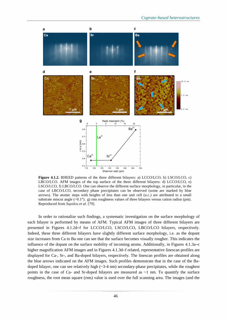
Cuprate-based heterostructures
46
Figure 4.1.2. RHEED patterns of the three different bilayers: a) LCCO/LCO, b) LSCO/LCO, c)
LBCO/LCO. AFM images of the top surface of the three different bilayers: d) LCCO/LCO, e)
LSCO/LCO, f) LBCO/LCO. One can observe the different surface morphology, in particular, in the
case of LBCO/LCO, secondary phase precipitates can be observed (some are marked by blue
arrows). The atomic steps with heights of less than one unit cell (u.c.) are attributed to a small
substrate miscut angle (~0.1°). g) rms roughness values of three bilayers versus cation radius (pm).
Reproduced from Suyolcu et al. [79].
In order to rationalize such findings, a systematic investigation on the surface morphology of
each bilayer is performed by means of AFM. Typical AFM images of three different bilayers are
presented in Figures 4.1.2d–f for LCCO/LCO, LSCO/LCO, LBCO/LCO bilayers, respectively.
Indeed, these three different bilayers have slightly different surface morphology, i.e. as the dopant
size increases from Ca to Ba one can see that the surface becomes visually rougher. This indicates the
influence of the dopant on the surface mobility of incoming atoms. Additionally, in Figures 4.1.3a–c
higher magnification AFM images and in Figures 4.1.3d–f related, representative linescan profiles are
displayed for Ca-, Sr-, and Ba-doped bilayers, respectively. The linescan profiles are obtained along
the blue arrows indicated on the AFM images. Such profiles demonstrate that in the case of the Ba-
doped bilayer, one can see relatively high (~3-4 nm) secondary-phase precipitates, while the roughest
points in the case of Ca- and Sr-doped bilayers are measured as ~1 nm. To quantify the surface
roughness, the root mean square (rms) value is used over the full scanning area. The images (and the

Cuprate-based heterostructures
47
linescan profiles) clearly demonstrate that Sr-doped and Ca-doped samples have atomically smooth
surfaces, whereas the Ba-doped sample is characterized by a remarkably rougher surface. In the case
of LCCO/LCO and LSCO/LCO bilayers, the rms roughness was measured as 0.377 nm and 0.376 nm
over a scanning area of 6.25 µm2. In the case of the LBCO/LCO bilayer, instead, the rms roughness is
0.805 nm, i.e. twice as large over the same scanning area. Most importantly, in the latter, secondary-
phase precipitates (indicated with light-blue arrows on Figure 4.1.2f), are detected as already
observed by RHEED during the growth. A plot of the rms surface roughness of the bilayers vs. the
dopant cation radius (pm) is presented in Figure 4.1.2g.
Moreover, with the aim of specifically addressing the Ba segregation issue, we have grown
more than 50 single-phase Ba-doped LCO epitaxial films with different Ba concentrations in the
range from 0.05 to 0.35 on LSAO (001) substrates. None of these films show ideal growth and are
free from formation of secondary phase precipitates. However, the critical thickness, at which
secondary phase precipitates nucleate, decreases linearly as the Ba concentration increases (Figure
4.1.3g). A typical RHEED image of a precipitate-free single-phase LBCO (x = 0.18) film with a
thickness less than the critical thickness (<5 u.c.) is shown in the bottom inset in Figure 4.1.3g, while
the upper inset is an RHEED image of a film thicker than the critical thickness of precipitate
formation for this doping level (> 6.5 u.c.). Note that the diffraction from the LBCO/LCO bilayer
exhibits a similar pattern with characteristic spots (cf. Figure 4.1.2). A typical AFM image of the 15
u.c. LBCO single-phase film, in which secondary-phase precipitates are clearly observed, is shown in
Figure 4.1.3h. For this particular sample, the rms surface roughness is ~1.74 nm, which is twice as
large as in an M–I bilayer with a 3 u.c. thick overdoped Ba layer. Furthermore, indirect observations
claiming that the precipitates are Ba-rich compared to precipitate-free areas are confirmed by using
Auger electron spectroscopy (AES). However, quantifying the chemical composition more precisely
is beyond the AES resolution. [79]

Cuprate-based heterostructures
48
Figure 4.1.3. High magnification AFM images of three different bilayers: a) LCCO/LCO, b)
LSCO/LCO, c) LBCO/LCO. Line scan profiles obtained from the AFM images given in a-c: d)
LCCO/LCO, e) LSCO/LCO, f) LBCO/LCO. One can observe the different surface morphology. In
the case of LBCO/LCO, secondary phase precipitations can be observed with up to 3-4 nm height.
g) The critical thickness of the LBCO film versus Ba concentration at which RHEED patterns
indicate nucleation of secondary phase precipitates. The top inset RHEED image has extra
diffraction spots in comparison to the bottom RHEED image. h) AFM image of a 15 u.c. thick
LBCO (x = 0.18) film on LSAO (001) substrate. Reproduced from Suyolcu et al. [79].

Cuprate-based heterostructures
49
For structural quality determination, first, XRD measurements are figured out, and the results
are compiled in Figure 4.1.4. From the position of Bragg peaks (00l), where l = 2, 4, 6, and 8, the
average c-axis lattice parameter for each bilayer was calculated and the results are presented in Figure
4.1.4a-c for Ca-, Sr- and Ba-doped bilayers, respectively. [52] Through the data, the shortest c-axis
lattice constant (13.22 Å) was observed for the LCCO/LCO bilayers, whereas the c-axis lattice
parameters are measured as 13.28 Å and 13.37 Å for the LSCO/LCO and LBCO/LCO bilayers,
respectively. XRD Ɵ–2Ɵ diffraction scans for three different bilayers demonstrate a single peak for
the two phases in a similar way to what was reported by Butko et al. [52]. Such findings nicely
correlate with the nominal cationic radii in nine-fold coordination as a consequence of Madelung
strain (Figure 4.1.4d).
Figure 4.1.4. XRD θ-2θ scans for three different bilayers: a) LCCO/LCO, b) LSCO/LCO, and c)
LBCO/LCO and d) c-axis lattice parameter versus ionic radii of dopants in three different bilayers:
LCCO/LCO, LSCO/LCO, and LBCO/LCO. Reproduced from Suyolcu et al. [79].
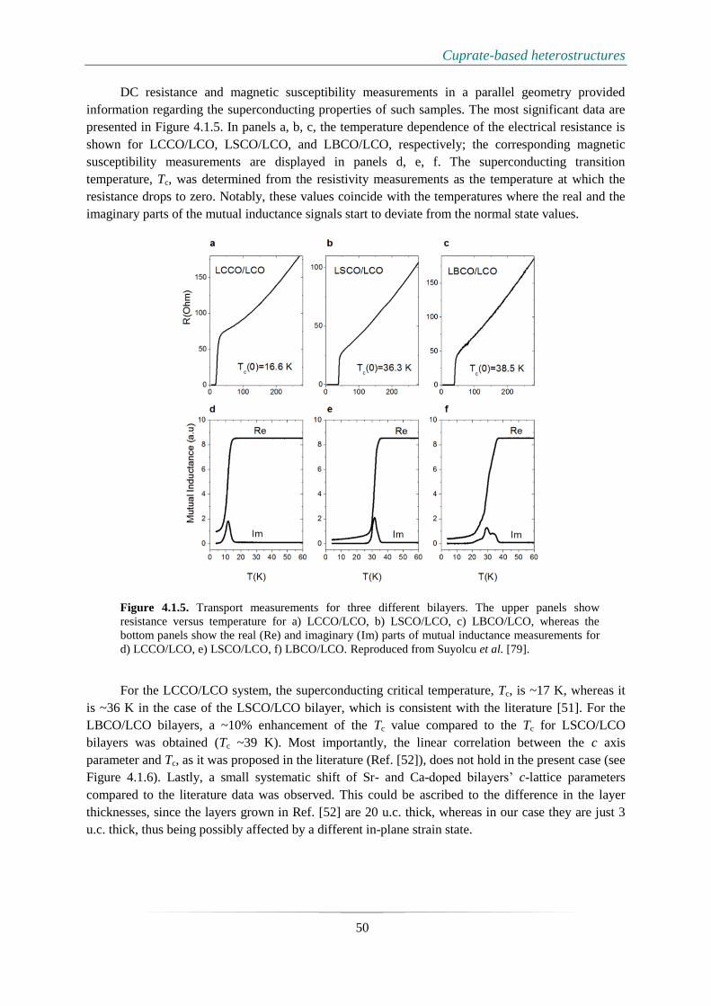
Cuprate-based heterostructures
50
DC resistance and magnetic susceptibility measurements in a parallel geometry provided
information regarding the superconducting properties of such samples. The most significant data are
presented in Figure 4.1.5. In panels a, b, c, the temperature dependence of the electrical resistance is
shown for LCCO/LCO, LSCO/LCO, and LBCO/LCO, respectively; the corresponding magnetic
susceptibility measurements are displayed in panels d, e, f. The superconducting transition
temperature, Tc, was determined from the resistivity measurements as the temperature at which the
resistance drops to zero. Notably, these values coincide with the temperatures where the real and the
imaginary parts of the mutual inductance signals start to deviate from the normal state values.
Figure 4.1.5. Transport measurements for three different bilayers. The upper panels show
resistance versus temperature for a) LCCO/LCO, b) LSCO/LCO, c) LBCO/LCO, whereas the
bottom panels show the real (Re) and imaginary (Im) parts of mutual inductance measurements for
d) LCCO/LCO, e) LSCO/LCO, f) LBCO/LCO. Reproduced from Suyolcu et al. [79].
For the LCCO/LCO system, the superconducting critical temperature, Tc, is ~17 K, whereas it
is ~36 K in the case of the LSCO/LCO bilayer, which is consistent with the literature [51]. For the
LBCO/LCO bilayers, a ~10% enhancement of the Tc value compared to the Tc for LSCO/LCO
bilayers was obtained (Tc ~39 K). Most importantly, the linear correlation between the c axis
parameter and Tc, as it was proposed in the literature (Ref. [52]), does not hold in the present case (see
Figure 4.1.6). Lastly, a small systematic shift of Sr- and Ca-doped bilayers’ c-lattice parameters
compared to the literature data was observed. This could be ascribed to the difference in the layer
thicknesses, since the layers grown in Ref. [52] are 20 u.c. thick, whereas in our case they are just 3
u.c. thick, thus being possibly affected by a different in-plane strain state.

Cuprate-based heterostructures
51
While the linear extrapolation of Tc vs c data would lead to a Tc 65 K, the measured value is
remarkably lower (only ~39 K). In addition, the transition to the superconducting state in the mutual
inductance measurements of LBCO/LCO bilayer is broad ranging from 38.6 K to 20 K with several
peaks in the real part, suggesting the presence of regions having different superconducting critical
temperatures (Figure 4.1.5f). An overview of the main results including surface roughness, average c-
axis lattice constant, and Tc is presented in Table 1. There exists a strong impact of different cations
on the superconducting and structural properties of bilayers grown under the same conditions.
Figure 4.1.6. Dependence of Tc on the average c-axis lattice parameter. The red squares show the
Tc values measured in Ca-, Sr-, and Ba-doped bilayers in the present study, whereas the black
circles refer to I–M (La2CuO4 / La1.56Sr0.44CuO4), S (superconducting; La2CuO4+ δ ), M–I
(La1.56Sr0.44CuO4 / La2CuO4) and M–S (La1.56Sr0.44CuO4 / La2CuO4+δ) structures as reported in Ref.
[52]. Reproduced from Suyolcu et al. [79].
Table 1. Summary of electrical and structural measurements for Ca, Sr, and Ba doped bilayers.
Structure Tc (K) (from
inductance)
Tc (K) (from
resistance)
Roughness
[nm]
c-axis
parameter [Å]
LCCO/LCO 16.1 16.6 0.37(7) 13.21(98)
LSCO/LCO 35.8 36.3 0.37(6) 13.27(53)
LBCO/LCO 38.1 38.6 0.80(5) 13.37(01)
In order to gain deeper insight on the interfacial situation and possibly on the discrepancy
between the present c vs Tc dependence in comparison with the literature, atomically resolved
imaging and spectroscopy were carried out by high-resolution STEM. High-angle annular dark-field
(HAADF) images taken from each bilayer proved the growth quality and defect-free structures.
Figure 4.1.7a depicts the microstructure of the LCCO/LCO bilayer. All atomically resolved HAADF
images were taken along the [100] direction of the LSAO substrate. The HAADF image, where the
contrast slightly changes in the first two unit cells from the substrate/LCCO bilayer interface,
demonstrates the high epitaxial quality of the LCCO/LCO bilayer, a coherent interface, and the
absence of extended defects such as misfit dislocations and/or stacking faults. An atomically resolved

Cuprate-based heterostructures
52
image at a higher magnification of the highlighted region in Figure 4.1.7a is presented in Figure
4.1.7b. Figure 4.1.7c shows the intensity profile of the HAADF image taken from the Ca-doped
bilayer presented in Figure 4.1.7a. The black arrow indicates the vertical length used for averaging
(Figure 4.1.7a). On the HAADF image, Ca-doped areas exhibit a darker contrast, while undoped LCO
layers appear brighter. Because the HAADF image intensity is approximately proportional to Z1.7−2
(where ZLa = 57 and ZCa = 20)) [33,105], the intensity increase in the first 1-2 unit cells corresponds to
the Ca-depleted region followed by a Ca-doped region with lower intensity. To the best of our
knowledge, this is the first example of a successfully grown overdoped LCCO epitaxial layer.
Figure 4.1.7. Atomically resolved STEM imaging and EELS spectrum imaging. a) HAADF image
showing the growth quality, a defect-free structure and coherent interfaces of LCCO/LCO. b) High
magnification of the area highlighted by the red rectangle in a. In d, f, and h, RGB elemental maps
(La = green, Cu = red, dopant = blue) are shown. In e, g and i the Ca-, Sr- and Ba-doped bilayers
dopant distributions, as obtained from the maps in (d), (f), and (h), are displayed. Reproduced from
Suyolcu et al. [79].
Figures 4.1.7d, 4.1.7f, and 4.1.7h show RGB (red is Cu, green is La, and blue is dopant) atomic
resolution maps of Ca, Sr, and Ba-doped bilayers as measured by EELS. The average profiles of the
dopant distributions obtained from the EELS maps are shown below each RGB map in Figures 4.1.7e,
4.1.7g, and 4.1.7i. The nominal interfaces are shown by black lines. To exemplify the base level for
the dopant signal observed, the Ba profile averaged from the RGB map of the Ba-doped bilayer (see
next section, Figure 4.2.2d) is presented in Figure 4.1.8 below.

Cuprate-based heterostructures
53
Figure 4.1.8. Dopant distribution of the Ba-doped bilayer as a plot of intensity vs. distance obtained
from the map in Figure 4.2.2d. The vertical lines indicate the nominal interfaces and dashed lines
indicate zero intensity. Reproduced from Suyolcu et al. [79].
The RGB maps and the average profiles of dopant distributions for Ca-, Sr-, and Ba-doped
bilayers exhibit characteristic differences. Sr-doped bilayers show the most homogeneous distribution
among the dopants (see Figures 4.1.7f and 4.1.7g). The abruptness of the LSCO/LCO interface can be
estimated from the decay of the Sr distribution from the M layer into I layer as 1.6 ± 0.4 nm, which
is in fairly good agreement with the values reported in the literature [10] for a related system.
Conversely, the distribution of Ca and Ba dopants in LCCO/LCO and LBCO/LCO bilayers is less
homogeneous. For averaging the distribution lengths from EELS line scans (for each dopant) several
line scans acquired from different regions of the samples are used.
The atomically resolved EELS RGB map shown in Figure 4.1.7h shows that the Ba
concentration increases in the M phase towards the LBCO/LCO interface. This trend is also
confirmed by the averaged profile of the Ba dopant presented in Figure 4.1.7i and clearly
demonstrates the tendency of Ba to segregate towards the free surface of the film. Most importantly,
as a consequence of such Ba migration, the LBCO/LCO interface is quite smeared, i.e. the decay
length of Ba ions, obtained as an average from several EELS linescans, is 2.6 ± 0.6 nm, which is
considerably larger with respect to the other dopants. Note that some linescans – as the one displayed
in Figure 4.1.8 – exhibit a Ba distribution involving the whole nominally undoped area. This may be
related to the presence of secondary phase precipitates at the film free surface as observed by RHEED
and AFM (see Figure 4.1.2).
As far as the LCCO/LCO bilayer is concerned, a tendency to Ca accumulation at the interface
between the substrate and the epitaxial layer is observed and is followed by a depletion of Ca on the
1st and 2
nd unit cells (see Fig. 4.1.7a-c). This is visible in the magnified RGB EELS map and average
Ca profile in Figures 4.1.7d and 4.1.7e, respectively. Such an anomalous behavior may be connected
with the compressive in-plane strain in the film and will be the object of further investigations. In this
case, the extent of cationic intermixing at the M–I interface can be estimated to be 1.4 ± 0.4 nm.
Please note that in this section, the RGB elemental maps obtained from each bilayer were presented,
however, in the next section, all elemental maps, i.e. La, Cu and each dopant Ba, Sr and Ca, for
individual atoms are displayed (Figures 4.2.3–4.2.5). The EEL spectrum images were processed using
the multivariate weighted principal component analysis routine (PCA) (MSA Plugin in Digital
Micrograph) developed by M. Watanabe [124] to reduce the noise in the data. In order to separate
overlapping edges in each spectrum, such as La-M5,4, Cu-L3,2, and Ba-M5,4, multiple linear least
square fitting (MLLS) [122] was used. For overlapped signals, MLLS fitting windows of 650–1100

Cuprate-based heterostructures
54
eV for Ba-M5,4, La-M5,4, Cu-L3,2, 305–390 eV for Ca-L3,2, and 1750–2100 eV for Sr-L3,2 edges were
used. The integration windows used for Ca-L3,2, Ba-M5,4, La-M5,4, Cu-L3,2, Sr-L3,2, and edges are 343–
394 eV, 772–815 eV, 822–868 eV, 935–961 eV, 1935–2066 eV, respectively.
Discussion
The present investigations highlight the profound impact that the choice of the dopant has on
the final structural properties of the bilayers, and how this affects the resulting electrical transport
properties of the system. In particular, it is observed that the average out-of-plane c-axis lattice
parameter as measured by XRD (Figure 4.1.4), which is an average over the whole thin-film volume,
exhibits a strong dependence on the dopant species, i.e., c is proportional to the dopant ionic radius
(the larger the dopant radius the larger is the lattice parameter) (Figure 4.1.4d). This allows us to tune
c simply by changing the dopant species while keeping the ionic charge constant. Interestingly,
although Ca2+
ions are smaller than La3+
ions, the Ca-doped bilayer has a larger c-axis lattice
parameter than pure LCO. This can be explained by the different valences of Ca (2+) and La (3+).
Ca2+
replaces La3+
and maintains the nine-fold coordination. Therefore, Ca2+
constitutes a negative
charge on the A-site. The electrostatic repulsion of this negative charge with neighboring oxygen ions
results in a lattice expansion.
A major impact of the dopant size on the in-plane strain state of the films is expected in a
similar way as was already demonstrated by Lee et al. for a related perovskite system. [99] In
particular, when Ba2+
is employed as a dopant, i.e. in the case of LBCO/LCO bilayers, the maximum
in-plane strain is induced. As the HAADF images show perfect epitaxial growth of all films without
formation of misfit dislocations or other defects which could relieve strain, the only way to obtain
strain relaxation in the case of the Ba-doped system is by the rearrangement of dopants within the
film, i.e. the segregation of excess Ba towards the film surface. This explains the formation of a
secondary phase (likely Ba-based) at the surface [75,77], as shown by AFM and RHEED images
(Figure 4.1.2c‒f) and revealed by AES. [79] It also explains, why in the case of single-phase films,
the critical thickness of precipitate formation during the growth is decreasing with increasing Ba
concentrations (see Figure 4.1.3g). The absence of such precipitates in LCCO and LSCO films
indicates that Ca2+
and Sr2+
ions, whose ionic size is more similar to La3+
, are accommodated in the
thin film, i.e. the in-plane strain is maintained. Our results are consistent with those of Lee et al. [99]
who found that the smaller size mismatch between the La3+
host and dopant cations reduces the
segregation level of the dopants. Notably, whereas a homogeneous dopant profile was found in the Sr-
doped bilayers, also the Ca-doped bilayers exhibit a certain tendency to inhomogeneity, i.e. Ca2+
accumulates towards the substrate possibly as a consequence of the strain state at the substrate-film
interface.
A strong deviation from the expected linear dependence of Tc on the c-axis lattice parameter for
M–I bilayers is revealed – with Tc of the LBCO/LCO bilayer being lower than expected – while the
c-axis lattice parameter is increased. Whereas the linear extrapolation of Tc vs c leads to a predicted Tc
65 K, the measured value is only ~39 K. In order to explain this, one needs to consider the dopant
distributions at each interface. The average cationic intermixing extent is as high as 2 u.c. in the case
of LBCO/LCO bilayers (the wide Ba distribution is also detected by EELS line scans (see Figure
4.1.8)). This anomalous Ba redistribution is a consequence of Ba segregation towards the film
surface, which eventually results in a particularly smeared M‒I interface. Such a finding can account
for the reduced Tc for the LBCO/LCO bilayers as demonstrated recently for a related LCO-based

Cuprate-based heterostructures
55
system, for which a smeared interface leads to classical doping, the so-called “homogeneous doping”
[55]. At equilibrium, the hole concentration is increased in correspondence to the randomly
distributed ionic dopant point defects, rather than to an interface effect, and defines the final local
physical properties. In such a situation (only homogeneous doping is active), one expects Tc not to
exceed the values which are normally obtained in doped single-phase systems, i.e. max Tc ~40 K for
optimally doped LBCO samples epitaxially grown on LaSrAlO4 (001) substrates [149]. The two
superconductivity mechanisms are illustrated in Figure 4.1.9 below.
Figure 4.1.9. Illustration of two different superconductivity mechanisms observed in M–I bilayers:
Interface superconductivity (HT-IS; i.e. Sr- and Ca-doping, top) vs. bulk superconductivity (HTSC;
i.e. Ba-doping, bottom). Due to different dopant distribution based on the dopant size (i.e. Ca and Sr
vs. Ba), different superconducting mechanisms are induced. The turquoise arrows indicate the
nominal M–I interface position.

Cuprate-based heterostructures
56
For both systems, despite a certain dopant redistribution is present at the interface, the behavior
is believed to be consistent with the typical HT-IS. In the case of the LSCO/LCO interface, as
investigated by Gozar et al. [10,136], Sr spread into the nominally undoped phase for about 1 u.c., i.e.
1.3 nm, in agreement with our observations on both LCCO/LCO and LSCO/LCO structures.
Nonetheless, these findings undoubtedly enable to ascribe the HT-IS to an electronic effect, rather
than to ionic doping. Therefore, in the present work, the reduced Tc of the LCCO/LCO interface (the
dopant spread beyond the interface is 1.4 nm), may be linked to the small c-axis parameter, in
agreement with the linear c–vs–Tc relation. The Sr-doped bilayers show consistency with the previous
studies, not only in Tc but also in the Sr redistribution length. [10]
Conclusions
In conclusion, a number of complementary experimental methods, including high-resolution
XRD, AFM, transport measurements and spherical aberration-corrected STEM-EELS is used in order
to study high-temperature superconducting interfaces in La1.6A0.4CuO4/ La2CuO4 bilayers grown by
atomic-layer-by-layer oxide MBE, where A = Ca2+
, Sr2+
, and Ba2+
. It is found that the c-axis lattice
parameter increases linearly with the dopant size. Tc was found to depend non-linearly on the average
c-axis lattice constant and saturates at about 40 K, whereas Tc was expected to rise up to about 70 K
for the LBCO/LCO case, due to the interplay between the hole leakage and Madelung strain. This is
assigned to a different redistribution of the dopant ions across the interface. In particular, as a
consequence of the large ionic size mismatch between the dopant and the host cation, Ba segregation
occurs and gives rise to a smeared interface. In the case of LCCO/LCO and LSCO/LCO systems, the
interfaces were found to be sharper (yet not atomically sharp). As a consequence of such a different
interface structure, distinct phenomena occur for inducing the interface superconductivity: in the
LCCO/LCO and LSCO/LCO cases, interface effects, i.e. electronic redistribution, are predominant,
whereas, in the case of LBCO/LCO, HTSC is rather ascribed to the “classical” homogeneous doping
determined by cationic intermixing. In such a “conventional” situation, the expected Tc enhancement
due to the interface effect is prevented.
This work highlights the profound impact that ionic intermixing may have on the definition of
the final properties of oxide epitaxial interfaces and demonstrates that future studies of ionic effects at
interfaces, in particular on cationic redistribution during growth, are of paramount importance for the
full understanding of such structures.
Cuprate-based heterostructures
57
4.1.2 Visualizing Jahn–Teller and anti-Jahn–Teller distortions
Introduction
Key properties of complex perovskite oxide structures are strongly influenced by small
structural changes of the BO6 octahedral network [151–155] and tailoring and tuning lattice
distortions can be achieved by strain states imposed, e.g., by the lattice mismatch between substrate
and film in epitaxial systems.[86,152,156–158] Thus, understanding how octahedral distortions are
correlated with dopant distribution and how they modify the functionality of complex oxide
heterostructures is of great significance.
The Jahn–Teller (JT) effect is a spontaneous geometric distortion of a non-linear system in an
electronic state with orbital degeneracy and results in removing the degeneracy via energy state
splitting and lowering its symmetry. [23] TMOs with octahedral coordination, in which the metal ion
has high-spin d4, low-spin d
7, and d
9 configurations, show JT distortions, which can be intimately
correlated with the physical properties [25]. For instance, the CuO6 octahedron in the parent La2CuO4
(LCO) is elongated along the c-axis by the JT effect [26] and exhibits two long and four short Cu–O
bonds. [27] Distortions of CuO6 in Sr-doped La2–xSrxCuO4 structures (x up to 0.4) and related changes
in Cu–O apical distances were studied via diffraction techniques providing average structural
information. [32] It is reported that, in such systems, increasing the dopant concentration determines
the compression of the octahedron (i.e. a decrease of the Cu–O apical distances) [32] defined as anti-
Jahn–Teller (AJT) effect. [26] Recently it was shown that, in the presence of interfacial electronic
redistribution leading to a decoupled concentration profile between electron holes and dopant ions
(striking interface effects), an anomalous elongation of the Cu–O apical distance in LCO-based
structures is present (JT distortion). [33,34] Thus, local JT distortions appear to be strongly related to
the presence of 2D interfacial superconductivity. Moreover, investigations on La2–xAxCuO4 (LACO)–
LCO bilayers [79] (where A is a divalent cation A = Sr, Ba, Ca) and two-dimensionally doped
La2CuO4 superlattices [33,55] pointed out that the dopant size and dopant distribution directly
influence the interface functionalities, i.e., the occurrence of the bulk-like or interfacial
superconductivity, as discussed in the previous section. In particular, the interfacial superconductivity
is induced only in the presence of a sharp interface. These findings pave the way for new promising
investigations on local distortions at such interfaces induced by different dopant distributions. In this
context, it is essential to probe the cation displacements and the octahedral tilts via a precise
determination of the atomic column positions and to correlate this with atomically resolved
information of the chemical composition.
In this work, new insights into LACO–LCO bilayers with differently sized dopants, i.e. A = Ba,
Sr, and Ca, having same formal valence state (2+), which allows systematically studying the effect of
the dopant size on octahedral distortions, are provided. Although octahedral distortions at the
interface of various heterostructures have been widely studied recently [151–153,159–161], the
present understanding of A2BO4 systems is, in this sense, still limited. Previous investigations of
LCO-based bilayers have been limited to Sr-doped systems [34] or, in the case differently sized
dopants have been used, no insights have been gained regarding the local lattice structural parameters
[79]. Here, by analyzing the cationic and anionic deformations with atomic resolution, it is shown that
the size mismatch between the dopant and the host La3+
cations directly affects the structure and in
particular the out-of-plane strain state. [99] It is further demonstrated that the dopant size locally
distorts both cationic (La‒La) and the anionic (O‒O sublattice) and different JT distortions are

Cuprate-based heterostructures
58
present. A comparative study gathered from hole-doped La2CuO4 structures combining different
STEM techniques (i.e. EELS, ABF, and HAADF imaging) which link the distribution of the dopants
with the CuO6 octahedral distortions is described.
Results
The substrate used for all the samples, i.e. LSAO, has a tetragonal structure with lattice
parameters a = 0.3754 nm and c = 1.2635 nm and bulk LCO has an orthorhombic structure, where
Cu–O planes are separated by two La–O planes. The lattice parameters of the bulk LCO are a =
0.5335 nm, b = 0.5415 nm, and c = 1.3117 nm. [52] Because of the small difference between the in-
plane lattice constants of LSAO and LCO and the existent epitaxial strain, the LCO film can be
considered as tetragonal. [88] Perfect coherent interfaces between the LSAO substrates and the
epitaxial layers are revealed through atomically resolved HAADF images (Figure 4.1.10. a‒c), which
cover the substrate and the nominal metallic and insulating phases, and demonstrate the high quality
of the bilayers. The substrate gives rise to a darker contrast as compared to the epitaxial layer due to
the difference of the mean atomic weight. [105]
Figure 4.1.10. STEM-HAADF images showing coherent interfaces of a) Ba- (LBCO), b) Sr-
(LSCO), and c) Ca- (LCCO) doped bilayers. The HAADF images were taken along the [100]
direction of the LSAO substrate. Reproduced from Suyolcu et al. [89].
Not only the temperature dependence of the electrical resistance for the samples, where all of
them exhibit a superconducting transition with critical transition temperatures (Tc) of ~39 K, ~36 K,
and ~17 K for Ba-, Sr-, and Ca-doped bilayers, respectively, but also their correlation with the dopant
size and distribution are discussed in the previous section. Now, the focus will be linking the dopant
distribution and the correlated lattice deformations, i.e. local lattice and octahedral distortions. First, I
start with the examination of the elemental distribution of each element employed in the structures,
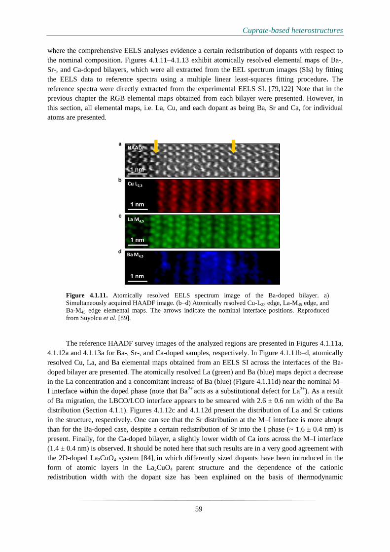
Cuprate-based heterostructures
59
where the comprehensive EELS analyses evidence a certain redistribution of dopants with respect to
the nominal composition. Figures 4.1.11–4.1.13 exhibit atomically resolved elemental maps of Ba-,
Sr-, and Ca-doped bilayers, which were all extracted from the EEL spectrum images (SIs) by fitting
the EELS data to reference spectra using a multiple linear least-squares fitting procedure. The
reference spectra were directly extracted from the experimental EELS SI. [79,122] Note that in the
previous chapter the RGB elemental maps obtained from each bilayer were presented. However, in
this section, all elemental maps, i.e. La, Cu, and each dopant as being Ba, Sr and Ca, for individual
atoms are presented.
Figure 4.1.11. Atomically resolved EELS spectrum image of the Ba-doped bilayer. a)
Simultaneously acquired HAADF image. (b–d) Atomically resolved Cu-L23 edge, La-M45 edge, and
Ba-M45 edge elemental maps. The arrows indicate the nominal interface positions. Reproduced
from Suyolcu et al. [89].
The reference HAADF survey images of the analyzed regions are presented in Figures 4.1.11a,
4.1.12a and 4.1.13a for Ba-, Sr-, and Ca-doped samples, respectively. In Figure 4.1.11b–d, atomically
resolved Cu, La, and Ba elemental maps obtained from an EELS SI across the interfaces of the Ba-
doped bilayer are presented. The atomically resolved La (green) and Ba (blue) maps depict a decrease
in the La concentration and a concomitant increase of Ba (blue) (Figure 4.1.11d) near the nominal M–
I interface within the doped phase (note that Ba2+
acts as a substitutional defect for La3+
). As a result
of Ba migration, the LBCO/LCO interface appears to be smeared with 2.6 ± 0.6 nm width of the Ba
distribution (Section 4.1.1). Figures 4.1.12c and 4.1.12d present the distribution of La and Sr cations
in the structure, respectively. One can see that the Sr distribution at the M–I interface is more abrupt
than for the Ba-doped case, despite a certain redistribution of Sr into the I phase (~ 1.6 ± 0.4 nm) is
present. Finally, for the Ca-doped bilayer, a slightly lower width of Ca ions across the M–I interface
(1.4 ± 0.4 nm) is observed. It should be noted here that such results are in a very good agreement with
the 2D-doped La2CuO4 system [84], in which differently sized dopants have been introduced in the
form of atomic layers in the La2CuO4 parent structure and the dependence of the cationic
redistribution width with the dopant size has been explained on the basis of thermodynamic

Cuprate-based heterostructures
60
considerations, i.e. equilibrium conditions establishing at the film surface during the growth process
(see the Section 4.2.1 for further details).
Figure 4.1.12. Atomically resolved EELS spectrum image of the Sr-doped bilayer. a)
Simultaneously acquired HAADF image. (b–d) Atomically resolved Cu-L2,3 edge, La-M4,5 edge,
and Sr-L2,3 edge elemental maps. The arrows indicate the nominal interface positions. Reproduced
from Suyolcu et al. [89].
The substrate-film interface (indicated by the left-hand side arrows in Figures 4.1.11 to 4.1.14)
presents a peculiar behavior depending on the dopant of choice: The Ba concentration is depleted in
the first layers of the M phase next to the substrate (see Figure 4.1.11), whereas a certain dopant
segregation (followed by a dopant depleted region) is observed at the substrate-film interface in the
Ca-case (see Figure 4.1.13). The Sr distribution in Sr-doped bilayers shows the most homogeneous
distribution within the nominally doped phase.
To evaluate the dopant distribution effect on the structure of the octahedral network, HAADF
(e.g. Figure 4.1.10) and ABF images (Figure 4.1.14) of the interfaces of all samples are
simultaneously acquired. Thus, all atomic columns in the crystal structure, namely La/Sr–O, Cu–O,
and O, were imaged. Subsequently, the interatomic apical (out-of-plane) and basal (in-plane) oxygen-
to-oxygen (O–O) distances were measured by using the O–O picker software. [125] Figure 4.1.14a–c
shows the atomically resolved ABF images, where all atomic columns are unambiguously resolved,
showing both nominal interfaces (i.e. substrate–M layer and M–I interfaces, for Ba-, Sr-, and Ca-
doped bilayers, respectively) confirming the high structural quality. In Figure 4.1.14d, the measured
interatomic distances are defined (the red arrow shows the distance between apical oxygen atoms, the
green arrow shows the distance between oxygen atoms in the basal plane).

Cuprate-based heterostructures
61
Figure 4.1.13. Atomically resolved EELS spectrum image of the Ca-doped bilayer. a)
Simultaneously acquired HAADF image. (b–d) Atomically resolved Cu-L23 edge, La-M45 edge, and
Ca-L23 edge elemental maps. The arrows indicate the nominal interface positions. Reproduced from
Suyolcu et al. [89].
Figure 4.1.14 ABF images showing coherent interfaces and all atomic column positions including
O-positions for the a) Ba-, b) Sr-, and c) Ca-doped bilayers. The yellow arrows indicate the nominal
interface positions. d) Illustration of measured apical and basal O–O distances on a magnified (and
colored) section obtained from (b). Reproduced from Suyolcu et al. [89].

Cuprate-based heterostructures
62
By averaging the dopant intensity profiles (i.e. Ba-M4,5, Sr-L2,3, Ca-L2,3) from elemental EELS
SIs (e.g. Figures 4.1.11–4.1.13), integrating the intensities for each constituting block (i.e. half unit
cell), summing up the values of all the constituting blocks, and scaling the doping concentration
profiles in order to preserve the global stoichiometry, the dopant concentrations (x) for each
constituting block, as shown in Figure 4.1.15a–c, are obtained. Measured interatomic distances vs.
number of CuO2 planes (or LCO blocks) are displayed in Figure 4.1.15d–f. The basal and apical O–O
interatomic distances are plotted in green and in red, respectively. Each data point corresponds to one
measured LCO block (i.e. half unit cell). The O–O interatomic distances were calibrated according to
the distances measured in the LSAO (001) substrate.
Figure 4.1.15 Graphs showing the concentration per CuO2 block for the a) Ba-, b) Sr-, and c) Ca-
doped bilayers. The horizontal dashed lines delimitate the region corresponding to the
superconducting phase. (d–f) O–O atomic column spacing along the apical (red) and basal (green)
directions for the LBCO/LCO, LSCO/LCO, and LCCO/LCO bilayers, respectively. The yellow
arrows indicate the nominal interface positions. The error bars represent the 95% confidence
interval (corresponding to 2 times the standard error) of the average of 14 unit cells of LCO along
the basal direction. Reproduced from Suyolcu et al. [89].

Cuprate-based heterostructures
63
All measurements of the basal in-plane O‒O distances for the three different bilayers exhibit
the same value within the error bars, namely 3.75 Å and exhibit a perfect coherency with the LSAO
substrate. These findings show that all films are under compressive in-plane strain. [33] Conversely,
in the LBCO/LCO system, a dramatic decrease of the apical oxygen distances with increasing Ba
concentration (Figure 4.1.15d) is observed. In the first half unit cell (i.e. the first LCO block) of the
epitaxial layer, the measured spacing is 4.72 ± 0.03 Å, whereas it is 4.51 ± 0.04 Å in the 6th LCO
block (next to the nominal interface). In the following column (the one just above the nominal
LBCO/LCO interface) the O–O apical distance is measured as 4.69 ± 0.030 Å. As far as the
LSCO/LCO bilayer is concerned, in the highly doped region, the O–O interatomic distances remain
constant (Figure 4.1.15e). However, a clear increase by 15 pm from the 8th (4.55 ± 0.03 Å) to the 9
th
atomic row (4.70 ± 0.05 Å) is found. Figure 4.1.15f indicates changes in the out-of-plane interatomic
distances in the LCCO/LCO bilayer related to the Ca dopant distribution. In particular, large O–O
distances were obtained for the first two unit cells, where the Ca concentration is less than the
nominal doping level. The value measured for the 2nd
epitaxial block is 4.68 ± 0.042 Å and the lowest
values of around 4.56 Å are obtained for the 5th and 6
th blocks yielding a decrease of the O–O
interatomic distance of 12 pm. Lastly, a gradual increase starting from the 6th block is observed and
the difference between 6th (4.56 ± 0.04 Å) and 10
th (4.71 ± 0.03 Å) blocks is measured as 15 pm.
In order to gain deeper insights into the effects of dopant size and distribution on local A-site
displacements, the basal and apical La–La atomic distances are measured. Figure 4.1.16 presents the
measured distances for each sample along with one representative HAADF image (from the
LBCO/LCO bilayer, Fig. 4.1.16a). The graphs (Fig. 4.1.16b–d) show La–La distances vs. number of
CuO2 planes (each plane corresponding to a building block of the LCO structure). In the LBCO/LCO
bilayer, the largest and the smallest interatomic La–La apical distances are measured for the 2nd
and
10th blocks as 3.73 ± 0.03 Å and 3.63 ± 0.02 Å, respectively, and exhibit a difference of ~10 pm
between nominally overdoped and undoped regions (Figure 4.1.16b). Moreover, a decrease of ~7 pm
is measured from the 6th block (3.71 ± 0.04 Å) to the 7
th block (3.64 ± 0.03 Å), which corresponds to
the nominal M–I interface. In the LSCO/LCO system (Figure 4.1.16c), the La–La distances in the
overdoped layers are slightly smaller than the LBCO/LCO system (i.e. ~3.67 Å). Also here, lower
La‒La distance values (up to 7–8 pm difference for the 10th block (3.61 ± 0.03 Å, where x (Sr) = 0),
are found for the undoped region with respect to the doped one. Figure 4.1.16d shows the results for
the LCCO/LCO bilayer: Here, only a slight monotonic increase of the La‒La distance in the growth
direction is observed, yet mostly lying within the experimental error bars. The average La–La
distance is 3.64 Å, where the highest value obtained is 3.66 ± 0.03 Å (5th block). To specifically
address the dopant size effect on local La–La distortions, the local apical distances averaged from the
six nominally overdoped layers (blocks 1–6) of each sample are compiled. The measurements reveal
that the largest La–La apical spacing (average) (3.71 ± 0.01 Å) is observed for the Ba-doped bilayer,
whereas the measured spacings are 3.67 Å and 3.63 Å for the Sr- and Ca-doped bilayers, respectively.
Figure 4.1.17 shows a plot of La–La distances vs. cation radii indicating the linear correlation.

Cuprate-based heterostructures
64
Figure 4.1.16. High-resolution STEM-HAADF image and quantitative analyses of the structural
distortion in the Ba-, Sr-, and Ca-doped bilayers: a) representative STEM-HAADF image of
LBCO/LCO bilayer given as a guide for the eyes; b), c) and d) La–La atomic column spacings
along the basal (green) and apical (red) directions for the Ba-, Sr-, and Ca-doped bilayers,
respectively. The error bars represent the 95% confidence interval (corresponding to 2 times the
standard error) of the average of 14 unit cells of LCO along the basal direction. Reproduced from
Suyolcu et al. [89].

Cuprate-based heterostructures
65
Figure 4.1.17. Dependence of local lattice parameter on the cation radii of dopants (i.e. Ba2+
, Sr2+
,
and Ca2+
). Reproduced from Suyolcu et al. [89].
Discussions
Previous investigations pointed out that the choice of the dopant has a profound impact on the
interface functionalities of the system. [79] From the EELS investigations, different profiles of dopant
distribution for Ba-, Sr-, and Ca-doped bilayers were obtained. Figure 4.1.15a–c summarizes the
dopant concentrations and gives quantitative information about the composition of each block. It is
known from the electronic phase diagram of the hole-doped lanthanum cuprate system that the
superconducting phase in bulk systems occurs when the doping level of a La2CuO4 unit cell lies
between 0.05 ≤ x ≤ 0.26. [47] At lower doping levels an insulating phase is present (underdoped),
whereas a metallic (overdoped) phase appears at x > 0.26.
Let us first consider the LBCO/LCO system. According to the dopant concentrations from the
EELS analyses (Figure 4.1.15a), it is evident that the blocks mostly exhibit metallic and
superconducting phases. This is a consequence not only of Ba distribution at the M‒I interface but
also of Ba depletion at the substrate‒M region. Moreover, blocks 5 to 7 are overdoped (i.e. metallic),
whereas most of the other columns (blocks 1 to 4) and in the nominally undoped phase (blocks 8 to
10) show compositions which can be ascribed to the superconducting phase. This indicates that, due
to ionic intermixing (i.e. to ionic doping), superconductivity should not be ascribed to effects arising
at the M‒I interface, rather it is a bulk phenomenon involving several unit blocks which is also
evidenced via previous mutual inductance measurements. [79]
If we now turn the attention to the O–O distances of the LBCO/LCO system, the measurements
performed on the ABF images (Figure 4.1.14) (with an assumption that no significant displacement of
Cu atoms occurs from the center of the CuO6 octahedron) demonstrate the decrease of the apical O–O
distance with increasing Ba doping along the growth direction. The smallest apical O–O distance
appears at the 6th constituting block, where the highest Ba concentration is present. Above the
nominal interface position (indicated by the yellow arrows in Figure 4.1.15a,d), the apical Cu‒O
distance starts to increase with a gradual decrease of the Ba concentration. This relationship between
the Ba concentration and the apical Cu‒O distance presents a clear example of an AJT distortion. [26]
Therefore, the correlation between the gradient in the Ba distribution and apical O–O distances on
both sides of the M–I interface could be ascribed to the AJT effect, which results in localization of
holes in both 𝑑𝑥2−𝑦2 and 𝑑𝑧2 orbitals. [89] At that point, one can argue that although a larger c-lattice

Cuprate-based heterostructures
66
parameter is obtained via Ba doping in both bulk [149] and epitaxially grown structures (e.g. single
phase films, M‒I structures etc.), intense AJT distortions causing shorter Cu‒O distances prevent
probable Tc enhancements. Such suggestion may be the object of further studies performed on Ba-
doped lanthanum cuprate systems similar to Sr-doped structures. [162]
As far as the Sr-doped bilayers are concerned, the obtained concentration profile shows a
homogeneous distribution in the overdoped layer, which exhibits the metallic composition (x >0.26,
see Figure 4.1.14), so that the HTSC stemming from “bulk” doping in the M-phase can be certainly
ruled out (unlike the above-described LBCO‒LCO system). A rapid fall-off in Sr concentration at the
M‒I interface is present. The compositional analysis suggests that blocks 7 and 8 (nominally
undoped) exhibit a non-negligible Sr concentration due to dopant redistribution in growth direction
(Figure 4.1.15b) [84]. It should be noted that the system under consideration is very similar to the one
which has extensively been studied by Gozar et al. [10], in which it was demonstrated that, despite a
certain ionic intermixing (whose width is very similar to what is reported here), hole redistribution
from the metallic into the insulating phase was highlighted and indicated as responsible for the HT-IS.
This has seen further confirmation in recent studies on related systems. [55,136]
Given the homogeneous Sr distribution in the overdoped layer, the AJT effect for the Sr-doped
sample cannot be discussed directly, as the O–O distance variations are almost as small as the
measurement precision (about 4 pm). [125] However, a considerable increase of the O–O apical
distance starting from the 9th block is observed. Such an “anomalous expansion” has been previously
reported for similar systems [33,34], in which the relation with the occurrence of HT-IS as a
consequence of interface effects (i.e. interface hole redistribution) was clearly demonstrated. [51]
Therefore, the observed sharp increase in apical O–O distance starting from the 9th block (JT
distortion indicating localized holes in 𝑑𝑥2−𝑦2 orbitals) can be considered as a fingerprint for a
superconducting transition induced by interface phenomena, not by “ordinary” ionic intermixing.
Notably, this sets a clear difference between the LBCO‒LCO system and the LSCO‒LCO system.
For the LCCO/LCO interface, a combination of both AJT (in the metallic phase) and JT
(starting from the interface) distortions is revealed. The situation in the M-phase is similar to what has
been described for the LSCO‒LCO case, i.e. the dopant concentration x lies above the limit for
HTSC, thus HTSC has to be ascribed to the M‒I interface region. In order to rule out any contribution
to superconductivity stemming from the presence of interstitial oxygen in LCO, all the samples have
been post-annealed in vacuum after the growth process (see Bauitti et al. [150]). Also, the dopant
redistribution length of the Ca-doped bilayer at the M‒I interface is comparable to the Sr-doped one.
A certain Ca accumulation at the substrate-film interface (zeroth block in Figure 4.1.14c – due to
epitaxial compressive stress, which may be partially accommodated by the substitution of La with
smaller Ca), is noticed and followed by the presence of a Ca-depleted region (i.e. 1st and 2
nd blocks).
An increase (~ 10 pm) of the apical O–O distances that is accompanied by such a lower dopant
concentration is followed by a decrease starting from block 3, in which a higher dopant content is
present. This again represents an AJT effect similar to the overdoped layer of the Ba-doped sample. A
monotonic increase (up to 15 pm) of the apical O–O distance is present from the 7th block (4.56 Å) to
the 10th block (4.71 Å). Importantly, blocks 9 and 10 do not exhibit the presence of any Ca-dopant,
thereby a typical JT distortion is observed, which – unlike what was observed for the M phase –
cannot be ascribed to the presence of dopant. Rather, given the superconducting character of the
interface, such a JT distortion may be related to 2D interfacial superconductivity in a similar way as
discussed for the Sr-case.
Cuprate-based heterostructures
67
It is revealed by detailed analyses that the JT distortion is present only in the case of Sr- and
Ca-doped M–I bilayers. In the case of the Ba-doped bilayer instead, AJT distortions characterize both
sides of the nominal interface of LBCO/LCO. Such a relationship between the dopant concentrations
and the out-of-plane O–O distances points towards two different superconducting mechanisms,
activated by the different dopant distributions leading to different JT distortions. In particular for bulk
superconductivity for the Ba-doped case, a typical AJT distortion (holes located in both 𝑑𝑥2−𝑦2 and
𝑑𝑧2 orbitals with parallel spins, resulting in shorter O–O distances) [29] is observed, whereas for the
Sr and Ca case a combination of AJT and JT is revealed, where the holes are located only in 𝑑𝑥2−𝑦2
orbitals and the apical oxygens are shifted away from the La sites resulting in larger O–O (apical)
interatomic distances. As described above, this may be related to the presence of interface effects
characterized by electronic redistribution.
Another point regards the local effect of substituting La3+
cations with differently sized dopants
having the same valence states (i.e. Ba2+
, Sr2+
, and Ca2+
). Figure 4.1.16 presents quantitative
information on local lattice deformation obtained from the HAADF images. Figure 4.1.16b shows
that the La–La apical distance in the LBCO system sharply decreases from the doped (M) to the
undoped (I) phase, substantiating that the large Ba dopant expands the lattice dramatically. A similar
effect, yet less pronounced, can be observed for the LSCO/LCO system, in which a decrease of apical
La–La distances from the M to the I phase is unveiled, again highlighting the lattice expansion due to
Sr substitution. The almost constant La–La spacing obtained from the Ca-doped bilayer instead
(Figure 4.1.16d) can be explained by the relatively small size difference between Ca2+
and La3+
,
which does not induce very large A-site displacements. These findings further suggest that apical O
displacements are more sensitive to the dopant size compared to La3+
displacements, indicating that
A-site deformations are relatively less affected (Figures 4.1.15 and 4.1.16).
Conclusions
In conclusion, the effect of dopant size and dopant distribution on the structure and the
octahedral network of ALL-oxide MBE grown La1.6M0.4CuO4 / La2CuO4 bilayers with M2+
= Ba2+
,
Sr2+,
and Ca2+
is studied. It is found that the different dopant size remarkably affects the structure as a
consequence of different dopant distribution in the structure. Atomically resolved EELS analyses
allowed us to reveal the elemental distributions across the interfaces and to measure the redistribution
lengths of the dopants in the growth direction as well as in the substrate. The interatomic distance
measurements performed on the ABF and HAADF images enable us to precisely determine the
atomic column positions and to quantitatively investigate the octahedral distortions and local lattice
deformations. Our findings revealed that the dopant distribution has a remarkable effect on the O–O
distance (JT and anti-JT effects), which can be related to the occurrence of different mechanisms
leading to superconductivity, and also unveiled the correlation between the dopant size and the local
lattice parameter. This work underlines the crucial effect of the dopant distribution on the octahedral
network and, in turn, on the final superconducting properties, and highlights the importance of
complementary advanced STEM techniques for the study of oxide interfaces.

Cuprate-based heterostructures
68
4.2 δ-doped high-temperature superconducting La2CuO4 interfaces
Introduction
Two-dimensional doping, i.e. “delta (δ)-doping”, which has been firstly reported for the
semiconductor field, is based on placing a very thin (i.e. single) layer of the dopant in a matrix or
substituting an atomic layer of the dopant with the host atoms, and suggests a new approach for oxide
materials. [163–167] At oxide materials interfaces, as a consequence of charge redistribution, a spatial
separation between ionic and electronic dopants may be obtained leading not only to increased
electronic mobility due to reduced scattering [168–170] but also to the occurrence of significant
functionalities. Recently, implementation of such an approach for achieving two-dimensional doping
(δ-doping) in lanthanum cuprate (La2CuO4), which yielded the occurrence of HTSC upon the
substitution of selected single LaO planes with SrO ones, [55] is achieved. It is great of importance to
observe the formation of the space-charge zone on the downward side of the two-dimensionally Sr-
doped layers [17,171], resulting in single-layer confinement of superconductivity. [51]
Previous STEM investigations already substantiated the asymmetric Sr profiles at the
interfaces, where the dopant concentration profile is abrupt at the downward side of the interface and
rather spread in the growth direction. [33] Similar (asymmetric) profiles have been reported in the
literature for semiconductors and oxides, not only the δ-doped structures but also for heterostructures
in which different phases are combined consecutively [172,173]. It is also shown that the choice of
the layer sequence directly influences the sharpness of the interfaces [163,172–176]. For the
evaluation of the experimental findings, various models have been proposed such as a kinetically
limited process [177,178], surface Fermi-level pinning [163], surface roughness [179], surface
diffusion as a consequence of intrinsic defects [172,180]. It is well known that the local chemistry at
the interfaces has a direct impact on the functionalities of oxide heterostructure interfaces [181–185],
and thus, it is of crucial importance to investigate the cationic intermixing at such interfaces. In this
work, ALL oxide-MBE grown δ-doped La2CuO4 structures [150] are investigated, in order to reveal
the role played by different parameters on the chemistry of the interfaces. The growth optimization
and the fabrication of the structures have been already performed by Dr. F. Baiutti (MPI-FKF) [61]
and the details of the growth of the heterostructures can be found in Ref. [84]. The nominal
composition of the grown structures can be written as follows:
[AO-LaO-CuO2 + N x (LaO-LaO-CuO2)] x M,
in which N and M represent the spacing between the doped layers (expressed in a number of
constituting La2CuO4 “blocks” i.e. half of the unit cell) and M represents the number of superlattice
repetitions, respectively. For systematic investigations of the structure and the properties of the
samples, a combination of various techniques was carried out such as in-situ RHEED during growth,
AFM, electrical conductivity measurements, and atomically-resolved STEM imaging and
spectroscopy. The choice of the dopants and the synthesis conditions enabled evaluating the influence
of different parameters on the final dopant profiles. In this study, the focus is on the impacts of (i)
dopant size, (ii) valence of A cation, (iii) growth temperature and (iv) tensile strain induced by the
substrate on the dopant distribution profiles.

Cuprate-based heterostructures
69
4.2.1 Effects of dopant size and valance on cationic distribution
To elucidate the influence of the cationic size mismatch between the dopant and the host cation
on the distribution characteristics, similar to Suyolcu et al. [79], a series of samples have been
investigated, where the elastic strain, induced by the cationic substitution is expected to be the driving
force for the segregation of the dopant. [99] Here, the effect of the substitution of La in the doped
layer with differently-sized dopants, namely, Ca, Sr and Ba, is studied. Note that the size mismatch is
calculated as (RA - RLa) x 100/ RLa, in which RA and RLa are the ionic radii of the A and the La cations
(9 - fold coordinated) respectively, according to Shannon. [96]
Figure 4.2.1. a) Resistivity vs temperature curves for Sr (black line), Ba (blue line), Ca (orange
line) two-dimensionally doped La2CuO4 (N = 9). The resistance values have been normalized by
multiplication with the number of superlattice repetitions (M). b) AFM micrograph of Ba δ-doped
La2CuO4 multilayer indicating the high tendency of secondary phase formation in the structure.
Reproduced from Bauitti et al. [84].
In Figure 4.2.1a, the low-temperature resistance curves of representative samples are given
presenting the HTSC transition for all samples. [61] For the Sr-doped case, the temperature of zero-
resistance, Tc, reaches the highest value ~ 41 K as a consequence of space-charge effects and ionic
redistribution [55]. Lower Tc values are measured in the case of Ba- (Tc ~ 21 K) and of Ca-doped (Tc
~17 K) samples. For the Ca δ-doping case, the value of the critical temperature is found to be
consistent with the previous findings obtained for single-phase Ca-doped bulk La2CuO4 structures.
[77] In the case of Ba-doped samples, the reduced Tc with respect to single-phase Ba-doped La2CuO4
may be ascribed to the strong tendency of forming secondary phases during the growth which is also
revealed via AFM investigations (Fig. 4.2.1b), which may be destructive for the transport properties.
[149]The structure of the samples together with the concentration profile of each dopant has been
investigated by atomically resolved STEM imaging and spectroscopy. STEM-HAADF images and
atomically-resolved EELS elemental maps (i.e. spectrum images) obtained from all samples are
presented in Figure 4.2.2 and Figure 4.2.3, respectively. HAADF images for Ca-, Sr-, and Ba- two-
dimensionally doped La2CuO4 are displayed in (a), (b), and (c) of Figure 4.2.2, respectively. The
images exhibit that, in all three cases, high-quality epitaxial growth without any structural defects on
the LaSrAlO4 (001) substrates were achieved. The different contrast due to the different atomic
numbers, (ZCa = 20, ZSr = 38, ZBa = 56, and ZLa = 57) the doped regions seem darker; especially for Ca
and Sr doping cases (see Figures 4.2.2.a–b).

Cuprate-based heterostructures
70
Figure 4.2.2. HAADF images for a) Ca, b) Sr, and c) Ba δ-doped multilayers. All images exhibit
the structural quality of the samples. [84]
Furthermore, the results of the atomically resolved EELS analyses (i.e. elemental maps) and
related averaged profiles obtained for different elements, are respectively presented in panels a and b
of Figure 4.2.3 for the Ca-doped, in Figure 4.2.3c–d for the Sr-doped and in Figure 4.2.3e–f for the
Ba-doped cases. From the EELS analyses, it is clearly seen that the dopant distribution is not confined
in a single atomic plane, but it is rather spread (i.e. the asymmetric profile). This is valid not only for
the Sr-doped case as previously reported but also for the Ca- and the Ba-doped samples. For
quantifying the amount of the abovementioned redistribution in both the substrate (downward side of
the interface) and growth directions (upward side of the interface) EELS linescans have been
analyzed. The results of the averaged linescans are presented in Figure 4.2.3g, in which the
redistribution width is shown as a function of the dopant ionic size mismatch with La. Let us first
focus on the upward side of the interface (solid diamonds). Here, the results of Ca- (2.65 ± 0.34 nm)
and Sr-doped (2.25 ± 0.54 nm) heterostructures show the independent behavior of the redistribution
length on the cation size, while in the case of Ba (2.97 ± 0.60 nm) a wider distribution of the dopant is
observed. At the backward side (open circles), a remarkably larger redistribution length is measured
for Ca (1.89 ± 0.31 nm) with respect to Sr (0.96 ± 0.33) and Ba (1.23 ± 0.26). The trends highlighted
by the analysis of the redistribution width ratio (upward/downward) displayed in Figure 4.2.3h, which
shows very similar values for the Sr- and Ba-doped cases (highly asymmetric distribution, width ratio
~ 2.4), whereas, in the case of Ca, the distribution is more symmetric (width ratio ~ 1.4). Dr. Yi Wang
(MPI-FKF) is gratefully acknowledged for the support on Figure 4.2.3.
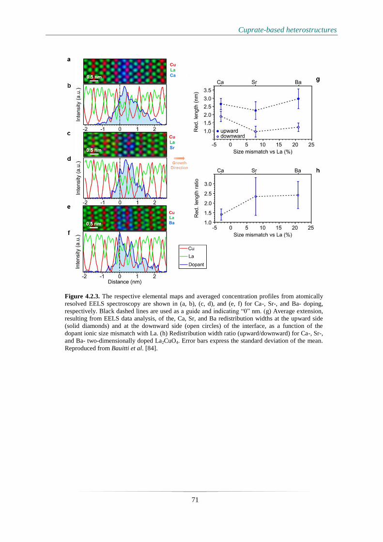
Cuprate-based heterostructures
71
Figure 4.2.3. The respective elemental maps and averaged concentration profiles from atomically
resolved EELS spectroscopy are shown in (a, b), (c, d), and (e, f) for Ca-, Sr-, and Ba- doping,
respectively. Black dashed lines are used as a guide and indicating “0” nm. (g) Average extension,
resulting from EELS data analysis, of the, Ca, Sr, and Ba redistribution widths at the upward side
(solid diamonds) and at the downward side (open circles) of the interface, as a function of the
dopant ionic size mismatch with La. (h) Redistribution width ratio (upward/downward) for Ca-, Sr-,
and Ba- two-dimensionally doped La2CuO4. Error bars express the standard deviation of the mean.
Reproduced from Bauitti et al. [84].
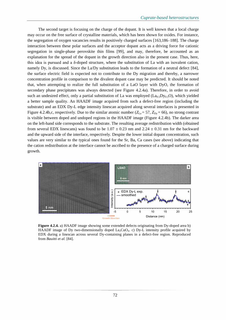
Cuprate-based heterostructures
72
The second target is focusing on the charge of the dopant. It is well known that a local charge
may occur on the free surface of crystalline materials, which has been shown for oxides. For instance,
the segregation of oxygen vacancies results in positively charged surfaces [163,186–188]. The charge
interaction between these polar surfaces and the acceptor dopant acts as a driving force for cationic
segregation in single-phase perovskite thin films [99], and may, therefore, be accounted as an
explanation for the spread of the dopant in the growth direction also in the present case. Thus, here,
this idea is pursued and a δ-doped structure, where the substitution of La with an isovalent cation,
namely Dy, is discussed. Since the La/Dy substitution leads to the formation of a neutral defect [84],
the surface electric field is expected not to contribute to the Dy migration and thereby, a narrower
concentration profile in comparison to the divalent dopant case may be predicted. It should be noted
that, when attempting to realize the full substitution of a LaO layer with DyO, the formation of
secondary phase precipitates was always detected (see Figure 4.2.4a). Therefore, in order to avoid
such an undesired effect, only a partial substitution of La was employed (La0.5Dy0.5O), which yielded
a better sample quality. An HAADF image acquired from such a defect-free region (including the
substrate) and an EDX Dy-L edge intensity linescan acquired along several interfaces is presented in
Figure 4.2.4b,c, respectively. Due to the similar atomic number (ZLa = 57, ZDy = 66), no strong contrast
is visible between doped and undoped regions in the HAADF image (Figure 4.2.4b). The darker area
on the left-hand side corresponds to the substrate. The resulting average redistribution width (obtained
from several EDX linescans) was found to be 1.07 ± 0.23 nm and 2.24 ± 0.31 nm for the backward
and the upward side of the interface, respectively. Despite the lower initial dopant concentration, such
values are very similar to the typical ones found for the Sr, Ba, Ca cases (see above) indicating that
the cation redistribution at the interface cannot be ascribed to the presence of a charged surface during
growth.
Figure 4.2.4. a) HAADF image showing some extended defects originating from Dy-doped area b)
HAADF image of Dy two-dimensionally doped La2CuO4. c) Dy-L intensity profile acquired by
EDX during a linescan across several Dy-containing planes in a defect-free region. Reproduced
from Bauitti et al. [84].
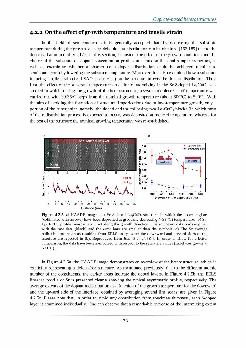
Cuprate-based heterostructures
73
4.2.2 On the effect of growth temperature and tensile strain
In the field of semiconductors it is generally accepted that, by decreasing the substrate
temperature during the growth, a sharp delta dopant distribution can be obtained [163,189] due to the
decreased atom mobility. [177] In this section, I consider the effect of the growth conditions and the
choice of the substrate on dopant concentration profiles and thus on the final sample properties, as
well as examining whether a sharper delta dopant distribution could be achieved (similar to
semiconductors) by lowering the substrate temperature. Moreover, it is also examined how a substrate
inducing tensile strain (i.e. LSAO in our case) on the structure affects the dopant distribution. Thus,
first, the effect of the substrate temperature on cationic intermixing in the Sr δ-doped La2CuO4 was
studied in which, during the growth of the heterostructure, a systematic decrease of temperature was
carried out with 30-35ºC steps from the nominal growth temperature (about 600ºC) to 500ºC. With
the aim of avoiding the formation of structural imperfections due to low-temperature growth, only a
portion of the superlattice, namely, the doped and the following two La2CuO4 blocks (in which most
of the redistribution process is expected to occur) was deposited at reduced temperature, whereas for
the rest of the structure the nominal growing temperature was re-established.
Figure 4.2.5. a) HAADF image of a Sr δ-doped La2CuO4 structure, in which the doped regions
(collimated with arrows) have been deposited at gradually decreasing (~35 ºC) temperatures. b) Sr-
L2,3 EELS profile linescan acquired along the growth direction. The smoothed data (red) is given
with the raw data (black) and the error bars are smaller than the symbols. c) The Sr average
redistribution length as resulting from EELS analyses for the downward and upward sides of the
interface are reported in (b). Reproduced from Bauitti et al. [84]. In order to allow for a better
comparison, the data have been normalized with respect to the reference values (interfaces grown at
600 ºC).
In Figure 4.2.5a, the HAADF image demonstrates an overview of the heterostructure, which is
explicitly representing a defect-free structure. As mentioned previously, due to the different atomic
number of the constituents, the darker areas indicate the doped layers. In Figure 4.2.5b, the EELS
linescan profile of Sr is presented clearly showing the typical asymmetric profile, respectively. The
average extents of the dopant redistribution as a function of the growth temperature for the downward
and the upward side of the interface, obtained by averaging several line scans, are given in Figure
4.2.5c. Please note that, in order to avoid any contribution from specimen thickness, each δ-doped
layer is examined individually. One can observe that a remarkable increase of the intermixing extent

Cuprate-based heterostructures
74
(up to 25% increase with respect to the interfaces grown at 600 ºC) can be found for the upward side
of the interface, while for the downward side the redistribution width does not exhibit a clear trend by
decreasing the growth temperature. This is in contrast with some experimental observations (and
relative models) related to semiconductor systems, which revealed, instead, the tendency of the
dopant to “freeze-in” closer to the nominal doped layer by lowering the growth temperature. [177]
Instead, it is observed that a change in the Sr concentration profiles occurs at the upward side of the
interface if the growth temperature is decreased below 565 °C. Moreover, the redistribution width
increases from about 3 nm (for growth T = 565−600 °C) to about 3.5 nm (for growth T = 535−500
°C) (see Figure 4.2.5d). Such a remarkable change can be attributed to the activation of the island
growth mode because of atoms clustering at low temperatures. [190] Correspondingly, when two
samples’ superconducting critical temperature (Tc) values are compared, lower Tc values are realized
for the sample grown in reduced (i.e. T = 500 °C) temperature. This can be again ascribed to the
activation of the island growth mode, having by virtue of the worsening of the sample crystallinity. It
should be noted here that, as far as the downward interface side is regarded, the independence of the
redistribution width with temperature can be easily explained by considering that during growth only
the upward side of each interface was deposited at reduced temperatures. Moreover, for what
concerns the portion of the structure which was grown under optimal conditions (T = 600 °C), the
slightly larger redistribution width which was observed here (~2.95 nm) with respect to the values
reported above (see Figure 4.2.3; ⁓2.25 nm), could be ascribed to the different sample thickness (
~50 nm here and ~25 nm in Figure 4.2.3), i.e., different times employed for the growth. As a
consequence, a longer time for thermal diffusion was allowed here.
Figure 4.2.6. a) HAADF image of a Sr δ-doped La2CuO4 multilayer grown on LSAT substrate
presenting the overview of the sample. White arrows indicate the δ-doped regions and orange
arrows indicate the structural defect. b) High magnification of the area highlighted by the blue
rectangle in a. c) Sr-L3,2 (red) and La-M5,4 (green) EELS profile linescans acquired along the growth
direction. Black arrows indicate the Sr distribution tendencies on both sides of nominal δ-doping
and dashed lines indicate zero intensity.

Cuprate-based heterostructures
75
The constructive effect of compressive strain (i.e. LSAO substrate) on HTSC in La2CuO4-based
systems is clearly shown [87] and such substrates have been highly in use. [16,79] The effect of
tensile strain on similar structures to unveil the influence on structural properties is studied as well.
For this purpose, the same structures (i.e. Sr δ-doped multilayers) grown on LSAT substrate, which
provides tensile strain instead of compressive strain as obtained by LSAO substrates, are examined.
Through the STEM investigations (Figure 4.2.6), two important findings based on imaging and
chemical analyses were obtained. First of all, in contrast with high-quality structures usually achieved
by using LSAO substrates, the epitaxial multilayers grown on LSAT substrates are characterized as
defective structures. Figure 4.2.6a demonstrates a defective region and orange arrows are used as
guides signaling the defect on the image. Atomically-Resolved EELS investigations also provide
interesting information. Such investigations, which are performed on defect-free regions along growth
direction (Figure 4.2.6c) substantiates the difference (i.e. change) in the Sr distribution in the
structure. In particular, the asymmetric profile tends to disappear in the growth direction. While the
first δ-doped layer in the structure provides a clear asymmetry in the profile, the redistribution profile
turns to a Gaussian-like distribution in the 4th two-dimensionally doped layer, which is proved by both
Sr and La linescan profiles (Figure 4.2.6c).
Discussion
A detailed investigation of the possible mechanisms determining the formation of cationic
intermixing at δ-doped La2CuO4 interfaces, in which the nominal structure is formed by substitution
of single LaO planes with AO dopant planes, is conducted. This enables addressing the main
mechanisms responsible for the dopant distribution at the downward side (substrate direction) and at
the upward side (growth direction) of the interface. The distribution in the substrate exhibits a higher
tendency to cationic intermixing in the case of the dopant having the smallest ionic radius (Ca) (see
Figure 4.2.3). Notably, in the substrate direction, the specific ALL-MBE growth kinetics, where the
dopant layer is deposited only once the underlying unit cell is completed, one can expect that the
intermixing occurs only either as a consequence of the roughness of the layer or due to thermal
diffusion (i.e. time-temperature dependent migration of the dopant into the bulk crystal). However,
detailed high-resolution STEM investigations do not indicate increased layer roughness for the Ca-
doped sample. Thus, it can be concluded that, on this side of the interface, intermixing occurs mainly
due to thermal diffusion (typically by the A-site vacancy hopping mechanism [191]). In this
framework, a smaller atomic radius is expected to lead to a reduced enthalpy in the diffusion process,
as already observed for related perovskite systems. [192] This may be also connected with the
compressive strain state (-1.4%) of the thin films, which may favor the substitution of La with a
cation having a smaller ionic radius. [193]
Importantly, if the Sr distribution is considered across the interface as reported by Wang et al.
[33], one can see that the distribution at the downward interface side can be satisfactorily fitted by
using a Gaussian distribution profile with a standard deviation σ = 0.43 nm as shown in Figure 4.2.7
(red line). Such a spatial distribution is expected by applying Fick’s law to an initial delta distribution.
By considering the usual growth time (t ~ 104 s), one can also estimate the diffusion coefficient D =
σ2/2t ~ 9 × 10
−20 cm
2/s. This is in good agreement with the typical diffusion coefficient value,s which
can be found in the literature for A2BO4 systems [143,192], referring to a counter diffusion of Sr2+
and
La3+
. The reason, why the differences between Ca, Sr, and Ba distribution profiles are rather limited,
could be the significant contribution of the La3+
migration. At the upward side of the interface,

Cuprate-based heterostructures
76
thermal diffusion is not explanatory itself alone, as it would lead to a symmetric Gaussian distribution
of the dopant cation across the nominal doped AO plane, whereas highly asymmetric profiles are
experimentally observed (see e.g. Figure 4.2.3k). According to the results obtained from Dy-doping
(cf. Figure 4.2.4), one can also conclude that the presence of a surface charge (during the growth)
cannot account for the dopant spread in the growth direction.
Figure 4.2.7. (a) Fitting of the Sr concentration profile across the nominally doped interface
(marked by the black dotted line). The blue circles represent the Sr experimental profile as retrieved
from the STEM-EELS analysis reported in ref 16. At the downward interface side, the experimental
data are fitted using a Gaussian function, which simulates the evolution of a delta-dopant profile
upon thermal diffusion. At the upward interface side, the fitting curve (green line) stems from the
Muraki equation, xn = x0(1 − P) Pn−1
, with fitting parameters x0 = 0.78 and P = 0.58. In particular,
the stars represent the resulting concentration of each (La,A)O−(La,A)O−CuO2 constituting block
(labeled with n). In panels b−d, a sketch of the cationic intermixing process based on
thermodynamical considerations is shown (“entropic model”). In panel b, the last undoped La2CuO4
constituting block (labeled with n = 1) is depicted on the surface of the film, together with the
incoming two-dimensionally doped La2CuO4 block (n = 2) (note that, for simplicity, the growth
process is pictured as “block-by-block” deposition, rather than as the real atomic-layer by atomic-
layer). Here the film (excluding the last La2CuO4 constituting block) is labeled as “bulk La2CuO4”.
Imposing the equilibrium conditions to be verified between the surface and the incoming block (n =
1 and n = 2) results in the A-cation being equally distributed between these two, as shown in panel c.
Afterwards, when the next block (n = 3) is deposited, the situation evolves as follows: n = 1 now
pertains to the bulk phase, i.e., is no more involved in the mixing process, whereas the blocks n = 2
and n = 3 share the same A-cation amount in order to establish conditions of thermodynamic
equilibrium. The resulting dopant distribution after this iteration is sketched in panel d (for each
step, the “active” blocks are highlighted in red). Such a process can be formally described by the
Muraki equation having P = 0.5 (dotted green line in panel a, resulting x0 = 0.69). Reproduced from
Bauitti et al. [84].
Furthermore, the in-plane strain induced by the ionic size mismatch between the host dopant
cation plays only a secondary role as demonstrated by the slightly larger redistribution width of Ba
with respect to Sr and Ca (in the growth direction, Figure 4.2.3). Rather, a mechanism that is based on
lateral diffusion during the growth should be taken into account, i.e. intermixing is allowed only
between the free film surface and the incoming particles (thus being limited to the topmost layer of
the film). This is justified by the fact that atom displacement at the surface requires only a limited
number of bonds to be broken, because of the lower coordination. Moreover, surface defects such as
steps or vacancies, which may arise as a consequence of growth imperfections, substrate morphology,
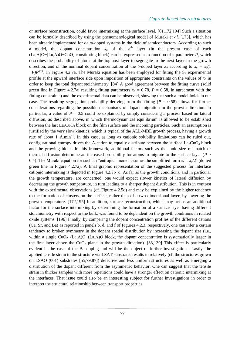
Cuprate-based heterostructures
77
or surface reconstruction, could favor intermixing at the surface level. [61,172,194] Such a situation
can be formally described by using the phenomenological model of Muraki et al. [173], which has
been already implemented for delta-doped systems in the field of semiconductors. According to such
a model, the dopant concentration xn of the nth layer (in the present case of each
(La,A)O−(La,A)O−CuO2 constituting block) can be expressed as a function of a parameter P, which
describes the probability of atoms at the topmost layer to segregate to the next layer in the growth
direction, and of the nominal dopant concentration of the δ-doped layer x0 according to xn = x0(1
−P)Pn−1
. In Figure 4.2.7a, The Muraki equation has been employed for fitting the Sr experimental
profile at the upward interface side upon imposition of appropriate constraints on the values of x0 in
order to keep the total dopant stoichiometry. [84] A good agreement between the fitting curve (solid
green line in Figure 4.2.7a; resulting fitting parameters x0 = 0.78, P = 0.58, in agreement with the
fitting constraints) and the experimental data can be observed, showing that such a model holds in our
case. The resulting segregation probability deriving from the fitting (P = 0.58) allows for further
considerations regarding the possible mechanisms of dopant migration in the growth direction. In
particular, a value of P = 0.5 could be explained by simply considering a process based on lateral
diffusion, as described above, in which thermodynamical equilibrium is allowed to be established
between the last La2CuO4 block on the film surface and the incoming particles. Such an assumption is
justified by the very slow kinetics, which is typical of the ALL-MBE growth process, having a growth
rate of about 1 Å.min−1
. In this case, as long as cationic solubility limitations can be ruled out,
configurational entropy drives the A-cation to equally distribute between the surface La2CuO4 block
and the growing block. In this framework, additional factors such as the ionic size mismatch or
thermal diffusion determine an increased probability for atoms to migrate to the surface layer (P >
0.5). The Muraki equation for such an “entropic” model assumes the simplified form xn = x0/2n (dotted
green line in Figure 4.2.7a). A final graphic representation of the suggested process for interface
cationic intermixing is depicted in Figure 4.2.7b−d. As far as the growth conditions, and in particular
the growth temperature, are concerned, one would expect slower kinetics of lateral diffusion by
decreasing the growth temperature, in turn leading to a sharper dopant distribution. This is in contrast
with the experimental observations (cf. Figure 4.2.5d) and may be explained by the higher tendency
to the formation of clusters on the surface, rather than of a two-dimensional layer, by lowering the
growth temperature. [172,195] In addition, surface reconstruction, which may act as an additional
factor for the surface intermixing by determining the formation of a surface layer having different
stoichiometry with respect to the bulk, was found to be dependent on the growth conditions in related
oxide systems. [196] Finally, by comparing the dopant concentration profiles of the different cations
(Ca, Sr, and Ba) as reported in panels b, d, and f of Figures 4.2.3, respectively, one can infer a certain
tendency to broken symmetry in the dopant spatial distribution by increasing the dopant size (i.e.,
within a single CuO2−(La,A)O−(La,A)O block, the dopant concentration is systematically larger in
the first layer above the CuO2 plane in the growth direction). [33,139] This effect is particularly
evident in the case of the Ba doping and will be the object of further investigations. Lastly, the
applied tensile strain to the structure via LSAT substrates results in relatively (cf. the structures grown
on LSAO (001) substrates [55,79,87]) defective and less uniform structures as well as emerging a
distribution of the dopant different from the asymmetric behavior. One can suggest that the tensile
strain in thicker samples with more repetitions could have a stronger effect on cationic intermixing at
the interfaces. That issue could also be an interesting subject for further investigations in order to
interpret the structural relationship between transport properties.
Cuprate-based heterostructures
78
Conclusion
In conclusion, a detailed investigation of the possible parameters affecting the redistribution of
the dopant in δ-doped La2CuO4 structures has been performed. Scanning transmission electron
microscopy investigations suggest that, in the direction of the substrate (downward interface side),
thermal diffusion is active and leads to the formation of a rather abrupt profile, if dopant substitution
is performed with cations having large ionic radii. On the other side, where the dopant is spread
across several unit cells, a thermodynamical model dominated by entropic effects is proposed. In
addition, layers roughness appears as a major factor in the cationic intermixing, whereas a prominent
role played by a surface space-charge layer and effects due to in-plane strain can be ruled out. Our
results emphasize the significant influence that interface chemistry plays in the definition of the final
properties of complex oxide heterostructures and may be employed for achieving better control of the
growth processes and of the final interface functionalities, e.g. by appropriately choosing the dopant
species, the growth conditions, and the substrates.

Cuprate-nickelate heterostructures
79
5. Cuprate-nickelate
heterostructures
Abstract
In this chapter, heteroepitaxial contacts of lanthanum cuprate and lanthanum
nickelate systems are presented. In particular, high-temperature superconductivity at
the interface of lanthanum cuprate (214) and strontium (Sr)-doped lanthanum
nickelate (214) heterostructures, and high-temperature thermoelectricity of lanthanum
cuprate (214) and lanthanum nickelate (113) heterostructures are discussed.
Atomically resolved scanning transmission electron spectroscopy and microscopy
techniques are combined with dedicated conductivity measurements, and local
structure and chemical properties are correlated with the functionalities of the
systems.
Cuprate-nickelate heterostructures
80
5.1 High-temperature superconductivity at La2CuO4/La2-xSrxNiO4
interfaces
Introduction
The approach of materials engineering through the introduction of an interface has seen early
development in the field of ionic and mixed ionic-electronic conductors, [171,197] which find wide
application e.g. in energy transformation and storage systems. In this class of functional materials,
significant deviations of the concentration profiles for the mobile ionic and electronic species may
occur at material discontinuities (e.g. grain boundaries and dislocations), potentially leading to huge
changes in the overall system functionalities (ionic and electronic conductivities). [198–201] Such
effects have been described in the light of the space-charge theory, according to which the interfacial
crystallographic discontinuity represented by an interface inherently determines the presence of an
electrical potential gradient that affects the concentration profiles of the mobile charge carriers in the
so-called space-charge zones in the interface region. [83,202]
La2CuO4-based HTSC systems are one of the widely studied oxide systems, where La2CuO4
(LCO) undergoes an insulator to high-temperature superconductor transition upon hole (h•) doping.
[40] Electron holes are normally introduced in the system (in the bulk form) as a compensating charge
for aliovalent ionic substitution or by introducing excess interstitial oxygen [74], but recent reports
importantly demonstrated that HTSC can be locally induced in LCO by taking advantage of interface
effects. [10,55,89,136] However, so far, such interfacial contribution has been limited to
homoepitaxial systems, in which the only employed phase was LCO-based, while the studies on
heterojunctions are still missing. Only one study of non-superconducting La2CuO4/La2NiO4 structures
was reported by Smadici et al. [203].
La2CuO4 and La2NiO4 (LNO) can be addressed by similar chemical and defect-chemical
considerations. Starting from the insulating stoichiometric compounds, an electronic phase
transformation can be achieved by increasing the electron hole concentration p = [h•]. In particular,
for the case of LNO a transition into a metallic phase with increasing p (up to p ~ 1.0) is observed,
[56] whereas high-temperature superconductivity (for 0.05 ≤ p ≤ 0.26) and metallicity (p > 0.26)
appear in LCO. [45,74] A hole increase can be generated in LCO and LNO by substituting La with an
acceptor dopant (mostly Sr+2
, denoted by SrLa′ i.e. Sr on La-site with a negative excess charge) or by
intercalating oxygen excess in the form of interstitial defects (Oi′′) [81,204,82] Taking into account
that both LSCO and LSNO can also accommodate a large amount of double-positively charged
oxygen vacancies (VO••), the electroneutrality condition reads:
p + 2 [VO••] = 2 [Oi
′′] + [SrLa′ ] (5.1.1)
The coupling between the various defect concentrations is determined by the mass action laws
of the respective interaction reactions (Frenkel-disorder reaction and oxygen incorporation reaction).
As a consequence, Sr-doping leads to an increased vacancy and decreased interstitial concentration.
[74] At interfaces equation 5.1.1 has to be replaced by Poisson’s equation leading to a redistribution
of all mobile charged defects. Therefore, a chemical potential gradient for holes and oxygen vacancies,
as well as for Sr, is present once a contact between nominally undoped LCO and LSNO is formed. In
Cuprate-nickelate heterostructures
81
order to establish equilibrium conditions, an interdiffusion of all the mobile defect species between
LSNO and LCO should take place, [83] which in turn is expected to affect the final conduction
properties of the interface region.
In order to investigate such a situation, superlattices of lanthanum cuprate (La2CuO4) and
lanthanum-strontium nickelate (La2‒xSrxNiO4) have been realized by atomic-layer-by layer oxide
MBE, which allows for precise control of the film stoichiometry at the atomic layer level. [150] For
the first time, it is demonstrated that interface HTSC can be induced in LCO at the heteroepitaxial
contact with LSNO. Furthermore, it is revealed that the final superconducting properties of the
LCO/LSNO interface can be effectively tuned by simply changing the structural parameters, (doping
level x of the nickelate phase, layers sequencing, and spacing), while leaving the stoichiometry of
LCO unchanged, unlike the “classical” bulk-doping picture.
In this part of the project, the main focus is established on high-resolution STEM investigations
(combined with other complementary techniques) including atomically-resolved imaging and
spectroscopy, which link the local structure and chemistry with the present functional properties.
Finally, the experimental findings are rationalized by discussing possible mechanisms for interface
charge redistribution. Superconductivity is rationalized by considering a mechanism for hole
accumulation at the interface based on local cationic intermixing but also on space-charge
considerations. The growth details and elementary characterization of the samples have been
previously initiated and discussed in Ref. [61]. In the latter stage of this project, I partially contributed
to the growth of the samples as well.
Results
All the superlattice structures are grown on LSAO (001) substrates inducing compressive strain
and the nominal composition of the superlattices can be written as:
1 x La1.56Sr0.44CuO4 + S x (2.5 x La2–xSrxNiO4 + N x La2CuO4)
Here, S represents the number of superlattice unit repetitions, whereas N defines the thickness of the
LCO phase (expressed in the number of unit cells – u.c.).
The resistance data for a representative set of samples having different doping level x of LSNO
are shown in Figure 5.1.1a, which demonstrates that HTSC forms with increasing x. In Figure 5.1.1b,
the Tc values as a function of the doping level are summarized. Superconductivity is found for x > 0.5,
reaching the plateau value of ~35–40 K for x > 0.8. While it is well known that single-phase LCO
undergoes an insulator-to-high-temperature-superconductor transition upon electronic doping, it is
important to note here that none of the constituting materials is expected to exhibit superconductivity.
Rather, HTSC is induced in the LCO phase at the interface region as a consequence of the contact
with the nickelate phase. As far as the temperature dependence of the resistance is concerned (∂R /
∂T), one cannot infer a clear correlation with the doping level x of LSNO. This, together with a certain
broadness, which characterizes the superconducting transition, is suggestive of spatial
inhomogeneities in the charge distribution or to a certain crystallographic disorder at the interface. In
Figures 5.1.1c and 5.1.1d, the electrical behavior of bilayers having different content x for LSNO is
reported. Such structures, in which LCO is either deposited as a bottom or as a top layer for LSNO,
allows for addressing the electrical properties of single-phase contacts. In Figure 5.1.1c (d), the R vs T
curve for a structure in which LCO is a bottom (top) layer is displayed. By comparing the two figures,
one can notice the superconducting properties are only slightly affected by the sequence of the layers,

Cuprate-nickelate heterostructures
82
i.e. the maximum Tc is in both cases 24 K. The analysis of the dependence of Tc on x suggests that the
minimum doping level for the occurrence of HTSC is slightly lower in the case of the LCO / LSNO
structure than in LSNO /LCO, as can be inferred by comparing the resistivity curves obtained for x =
0.7. As far as lower doping levels are concerned, one can expect Tc to exhibit a similar dependence on
x, as for what was already pointed out in the case of the superlattice structures (i.e. absence of
superconducting transition for x < 0.5 for both the LCO/LSNO and the LSNO/LCO contacts).
The dependence of Tc on the thickness of the LCO phase has been studied for the case of
superlattices in which x = 1.3 (Figure 5.1.2). The highest Tc values (Tc > 30 K) are obtained for 2.5
u.c. < N < 4.5 u.c.. For lower N values, Tc decreases (and the structure eventually becomes non-
superconducting for N = 1 u.c.). For large N ( > 4.5 u.c.), Tc tends to saturate at 25 K. This is
comparable with Tc obtained for the bilayers (cf. Figures 5.1.1c, and 5.1.1d).
In order to explain the dependence of Tc versus doping level x (cf. Fig 5.1.1b), dedicated STEM
investigations on LCO/LSNO/LCO interfaces (in the form of trilayer structures) – with compositions
x = 0.8 and x = 0.4 – are performed. Low-magnification STEM-HAADF images of each sample
covering the substrate and the epitaxial trilayers are displayed in Figure 5.1.3 demonstrating the high
structural quality of the films. Due to the different Sr concentrations (i.e. x = 0.8 and x = 0.4)
employed in the LSNO structures, the different contrast in the images is discernable: In the higher
doping case stronger contrast (Figure 5.1.3a) is obtained.
Figure 5.1.1: Electrical properties of LCO / LSNO structures. a) Resistance curves as a function
of temperature, for a set of superlattices (N = 2.5) having different doping levels x of LSNO. In
order to allow for a direct comparison between the curves, the resistance values have been
normalized to R (T = 273 K). b) Dependence of Tc on the doping level x for LCO / LSNO
superlattices for a set of representative samples (the corresponding R vs T curves are reported in (a)).
c) R vs T for LCO (bottom layer) / LSNO (top layer) bilayers and d) R vs T for LSNO (bottom
layer) / LCO (top layer) bilayers for representative doping levels x (refer to Figure 5.1.1a for the
color legend). Reproduced from Bauitti et al. [205].

Cuprate-nickelate heterostructures
83
Figure 5.1.2. Dependence of Tc with the LCO thickness for LCO / LSNO superlattices. a) R vs
T curves for 1 x La1.56Sr0.44CuO4 + S x (2.5 x La0.7Sr1.3NiO4 + N x La2CuO4) superlattices, for
different LCO thicknesses N. b) Tc values as a function of the thickness of the LCO phase N for the
La0.7Sr1.3NiO4/La2CuO4 superlattices, whose R vs T curves are reported in (a). Reproduced from
Bauitti et al. [205].
Figure 5.1.3. Low-magnification STEM-HAADF images of (a) x = 0.8 and (b) x = 0.4
LCO/LSNO/LCO trilayers. The images demonstrate the epitaxial quality and the defect-free
structures for both samples. Depending on the different doping (i.e. Sr doping) of the samples the
image contrasts are different.
Higher-magnification images focusing on both LCO/LSNO and LSNO/LCO interfaces as well
as related EDS linescans across the interfaces of each sample (i.e. x = 0.8 and x = 0.4) are presented in
Figure 5.1.4. In particular, for x = 0.8 (Figures 5.1.4a and 5.1.4b for HAADF imaging and EDX
linescan, respectively) HTSC arises, whereas insulating behavior is observed for x = 0.4 (Figures
5.1.4c and 5.1.4d for HAADF imaging and EDX linescan, respectively). On the HAADF images
(Figs. 5.1.4a,c) the nominal interface positions, identified by taking into account the LSNO thickness
and the number of Ni intensity maxima in the EDX linescans (cf. Figs 5.1.4b,d), are marked by red
and yellow arrows. While the Sr concentration initially undergoes a sharp drop on both interface sides,
whose spread has an upper limit of ~1 nm regardless of the doping level (by taking the nominal
interface positions as a reference), an additional Sr “tail”, indicated by a shaded blue arrow in Fig.

Cuprate-nickelate heterostructures
84
5.1.4b and 5.1.4d characterizes the LSNO / LCO contact (LCO as a top layer). This is wider for x =
0.8 (~2.5 nm) than for x = 0.4 (~1.5 nm). Such an asymmetric profile may be due to the combined
effect of thermal diffusion acting on both interface sides and of a “Muraki segregation effect”, the
latter acting in the growth direction only (i.e. at the LSNO/LCO contact), in analogy with a previous
study. [84] More interesting is the comparison between the Ni and Sr profiles, in consideration of the
fact that Ni impurities are known to act as a suppressor of HTSC in LCO. [206,207] In particular, the
redistribution length of the two species at the LCO/LSNO contact is of the same extent. Conversely,
the Sr migration width at the LSNO/LCO interface is larger (about 1 extra u.c.) than the Ni
redistribution width.
At this point, it is worth to focus on the comparison between the electronic and ionic
concentration profiles. For this purpose, a detailed examination of the O-K edge prepeak via EELS
analysis is performed on a LCO/LSNO superlattice having x = 1.3. In Figure 5.1.5, the STEM-
HAADF image and Sr, Ni and O-K edge prepeak profiles obtained from EELS are presented. The
STEM-HAADF image (Figure 5.1.5a) reveals the high-quality epitaxial relationship between the
substrate (dark region on the left-hand side) and the film, where the strong image contrast (cf. Figure
5.1.3) clearly shows the individual LCO and LSNO layers. An important point is the decoupling
between the Sr distribution (blue line in Figure 5.1.5c, top panel) and the O-K edge prepeak (red line
in Figure 5.1.5c, bottom panel), which indicates the decoupling between Sr and hole distribution
profiles, that is present at both interface sides.
Figure 5.1.4. STEM imaging and EDX spectroscopy for LCO / LSNO / LCO trilayers. In
panels a) and c), HAADF images of structures in which the doping level of LSNO are x = 0.8 and x
= 0.4, respectively, are displayed. EDX linescans for Ni and Sr are shown in panels b (for x = 0.8)
and d (x = 0.4). Reproduced from Bauitti et al. [205].

Cuprate-nickelate heterostructures
85
Figure 5.1.5. HR-STEM investigations at the La2CuO4 / La0.7Sr1.3NiO4 / La2CuO4 interfaces. a)
HAADF image of a the superlattice structure (N = 9). b) Spatial elemental distribution, extracted
from the EELS spectrum image across a La0.7Sr1.3NiO4 region and neighboring LCO areas (the
analyzed region is highlighted by the orange rectangle in panel (a) ). The color code is as follows:
La-green, Cu-red, Ni-orange, Sr-blue. c) EDX signal for Sr (blue) and Ni (orange) (top panel),
together with the simultaneously acquired O-K edge prepeak profile as obtained by an EELS
linescan (red line, bottom panel). The blue and red arrows indicate the upper limits for the Sr and
holes distributions, respectively. Reproduced from Bauitti et al. [205].
For precise evaluation of the O-K edge prepeak and Sr distribution simultaneous acquisition of
STEM-EDXS and STEM-EELS spectrum images are carried out across the interfaces (Figure 5.1.6).
The experimental (STEM-HAADF) survey image is presented in Figure 5.1.6a. Raw EDXS spectrum
images including all elements and background-subtracted EELS spectrum images of the O-K edge are
displayed in 5.1.6b,c, respectively. The O-K edge profiles obtained from different positions, i.e. from
the LCO and LSNO layers as well as both interfaces, LCO/LSNO (bottom) and LSNO/LCO (top), are
presented in Figure 5.1.6d, which demonstrates clear differences in the prepeaks. In particular, the
presence of the prepeak formation at both interfaces and in the LSNO layer confirms the O-K edge
prepeak mapping given in Figure 5.1.5, while no prepeak formation is observed in the LCO layer. Dr.
Yi Wang (MPI-FKF) is acknowledged for the valuable contribution on Figure 5.1.5.

Cuprate-nickelate heterostructures
86
Figure 5.1.6. (a) HAADF image showing the line along which the EELS and EDXS line scan was
acquired. (b) Raw EDXS spectrum image. (c) EELS spectrum image of the O-K edge after
background subtraction. (d) Oxygen-K edge from different positions as indicated in Figure (a). The
intensity of the pre-edge peak has been quantified by multi-Gaussian peak fitting using a non-linear
least square (NLLS) routine for all spectra in the line scan profile across several interfaces.
Reproduced from Bauitti et al. [205].
Discussion
Comprehensive STEM investigations clearly substantiate the elemental intermixing –
especially the Sr redistribution – across the interfaces. Although the occurrence of HTSC can be
partly attributed to the unintentional Sr doping of LCO, such Sr intermixing alone does not provide a
sufficient explanation for a number of experimental findings, therefore cannot be accounted as the
only responsible factor for the HT-IS.
In particular, as far the LSNO/LCO contact is concerned, a greater (~1 nm) Sr redistribution
width for the superconducting interface (when x = 0.8) with respect to a non-superconducting contact
(x = 0.4) is observed, and no difference in the chemical abruptness at the LCO/LSNO interface can be
detected, when comparing the superconducting interface (i.e. x = 0.8; Figure 5.1.4b) and the non-
superconducting interface (i.e. x = 0.4; Figure 5.1.4d). Therefore, the electrical properties are not
directly coupled to the Sr concentration profiles. Most importantly, the LCO/LSNO interface is not
only chemically sharper as for Sr, but it is also characterized by a similar migration width of Sr and
Ni, i.e. Ni impurities are present in the same LCO region, which is also doped by Sr. As it is well-
known in literature and as further corroborated by our experimental evidence, the presence of a small
percentage of Ni replacing Cu in the CuO2 planes is expected to determine a strong decrease of the
superconducting critical temperature, Tc. [206,207] Therefore, if cationic interdiffusion is taken as the
only responsible for the effects, superconductivity with Tc up to 40 K stemming from such Ni-
containing LSCO areas should be ruled out. Lastly, the comparison between the Sr dopant and the
hole profiles, as retrieved by STEM-EDXS profiles (Figure 5.1.5), indicates that an evident

Cuprate-nickelate heterostructures
87
decoupling between the two, i.e. the formation of a hole accumulation layer, is present at the interface.
Such a finding is clearly not ascribable to “simple” homogeneous doping, in which charge neutrality
is locally fulfilled according to equation (2.5) (which can be simplified as p = [𝑆𝑟𝐿𝑎′ ] in the hole
compensation regime).
A generalized thermodynamic picture that takes into account all these constituting elements has
to be paid attention to, [83] since in these systems both the ionic (cationic and anionic) and the
electronic species are sufficiently mobile to redistribute. [204] In order to describe the thermodynamic
equilibrium at an interface, one needs to consider the electrochemical potential �̃�𝑘 (for simplicity for
one direction, “x”) for each defect species k having effective charge 𝑧𝑘:
�̃�𝑘(𝑥) = 𝜇𝑘 +𝑧𝑘𝑒𝜑(𝑥) = 𝜇𝑘0 + 𝑅𝑇 log 𝑐𝑘(𝑥) + 𝑧𝑘𝑒𝜑(𝑥) (5.1.2)
in which the electrochemical potential at distance x from the interface is expressed as a function of the
standard chemical potential 𝜇𝑘0 , of the defect concentration 𝑐𝑘 and of the electrical potential 𝜑(𝑥)
(here 𝜇𝑘 represents the chemical potential for the defect k). In equation 5.1.2, the dilute carrier’s
concentration and hence the Boltzmann distribution are assumed for simplicity. In equilibrium, the
condition of a constant electrochemical potential demands
�̃�𝑘(𝑥) = �̃�𝑘,∞, (5.1.3)
�̃�𝑘,∞ = �̃�𝑘(𝑥 = ∞) being the electrochemical potential in the bulk (𝑥 = ∞).
The chemical potential gradient for the defect species (holes, oxygen vacancies, and Sr), which
is present at the interface between LSNO and LCO, is not only a driving force for the migration of Sr
in the direction of LCO, but also for the transfer of holes and oxygen vacancies. Owing to the
mobilities involved, the latter is expected to occur even at room temperature, while a Sr transfer
requires higher temperatures (possibly reached during preparation).
As far as the charge transfer direction is concerned, the entire free-energy picture has to be
considered. Here, the direction on the basis of the doping conditions (configurational entropy) is
estimated, supported by the chemical similarity of the base-materials. As the substantial Sr doping of
LNO enforces a very high hole and a very high vacancy concentration as long as electroneutrality has
to be fulfilled, suspending the latter condition is expected to result in a transfer of both carriers to the
undoped LCO provided Sr remains frozen (or to a Sr redistribution if sufficiently mobile). For the
Boltzmann distribution, the equilibrium spatial distribution in such a space-charge region follows
from combining equations 5.1.2 and 5.1.3:
𝑐𝑘(𝑥)
𝑐𝑘,∞= exp (−
𝑧𝑘𝑒∆𝜑(𝑥)
𝑘𝑇) (5.1.4)
𝑐𝑘,∞ being the defect concentration in the bulk and ∆𝜑(𝑥) = 𝜑(𝑥) − 𝜑(𝑥 = ∞) the space-charge
potential.
Equation 5.1.4 shows that oxygen vacancies and holes perceive the space-charge in a
qualitatively similar way, but the profile for 𝑉𝑂•• (zk = 2) is steeper than for ℎ• (zk = 1). A net transfer

Cuprate-nickelate heterostructures
88
of oxygen vacancies and holes from LSNO to LCO leads to the formation of a negatively charged
region at the LSNO side of the interface. For compensation, a region where oxygen vacancies and
especially holes (the holes being the majority defect in the system) are accumulated, establishes in
LCO. Such a situation with an enriched p-type charge carriers concentration eventually leads to the
occurrence of HTSC in LCO at the interface. A schematic picture of the thermodynamic situation at
the interface is depicted in Figure 5.1.7.
Such a space-charge situation is able to explain all the experimental findings: (I) From the
experimental data, it is evident that the key element for the appearance of superconductivity is the
enhanced hole concentration in LSNO. This suggests electron transfer (electronic space-charge): In
order to maintain the hole electrochemical potential constant (see equation 5.1.4) holes are transferred
from LSNO into the LCO phase leading to the appearance of HTSC. [84] Such a mechanism has
already found experimental proof in other oxides.[131,208] Interestingly, for high doping level (x ≥
0.9), single phase LSNO undergoes an insulator-to-metal transition as reported in literature [56] and
as confirmed by previous studies on MBE-grown LSNO films. [150] Such a value is very similar to
the doping level at which the superconducting state is fully developed in the structure studied here,
therefore suggesting that a charge transfer mainly involves delocalized holes from the metallic LSNO
phase to LCO. It should be noticed that this is also in line with previous contributions on a related
system (i.e. interface HTSC in LSCO/LCO bilayers), [140] in which a similar dependence of Tc with
the electronic carrier density of LSCO was found. (II) The hole‒Sr decoupling (cf. Figure 5.1.4d) can
be fully explained by considering that, in the space-charge regions, the concentration profiles of the
mobile defects are not dictated by the condition of local electroneutrality (cf. equation 5.1.1 and
equation 5.1.4). Rather, the migration of negatively charged Sr defects from LSNO to LCO is
expected to simply lower the space-charge potential 𝜑(𝑥), but to not directly influence the local hole
concentration. (III) As far as the effect of Ni impurities on HTSC is concerned, it is evident from
Figure 5.1.4d that the extent of the hole accumulation (space-charge) zone at the interface, in which
HTSC is expected to appear, is larger than the Ni redistribution width. (IV) The dependence of Tc with
the superlattice spacing N (Figure 5.1.2) can be explained by taking into account that for low spacing
(for which reduced Tc was found) one expects the space-charge zones to overlap leading to high hole
concentration. The reduced Tc ~ 25 K which has been observed for very large spacing (N > 5), as well
as for the bilayers (Figure 5.1.1c and 5.1.1d), may instead be ascribed to out-of-plane adjustments of
the lattice bond lengths as a consequence of the epitaxial relation between the layers. [52,61] Few
very recent studies have dealt with the origin of the electrical and magnetic properties of oxide
epitaxial heterostructures in the light of the space-charge theory. [209,210]
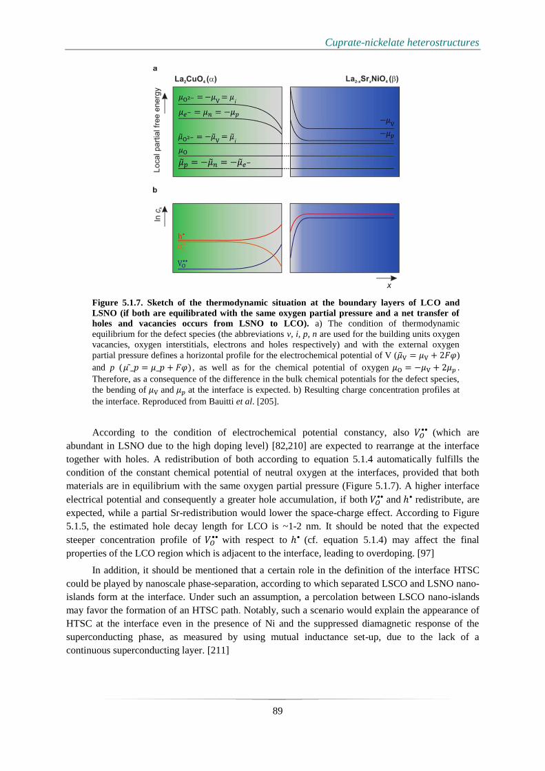
Cuprate-nickelate heterostructures
89
Figure 5.1.7. Sketch of the thermodynamic situation at the boundary layers of LCO and
LSNO (if both are equilibrated with the same oxygen partial pressure and a net transfer of
holes and vacancies occurs from LSNO to LCO). a) The condition of thermodynamic
equilibrium for the defect species (the abbreviations v, i, p, n are used for the building units oxygen
vacancies, oxygen interstitials, electrons and holes respectively) and with the external oxygen
partial pressure defines a horizontal profile for the electrochemical potential of V (�̃�V = 𝜇V + 2𝐹𝜑)
and p (𝜇 ̃_𝑝 = 𝜇_𝑝 + 𝐹𝜑) , as well as for the chemical potential of oxygen 𝜇O = −𝜇V + 2𝜇𝑝 .
Therefore, as a consequence of the difference in the bulk chemical potentials for the defect species,
the bending of 𝜇V and 𝜇𝑝 at the interface is expected. b) Resulting charge concentration profiles at
the interface. Reproduced from Bauitti et al. [205].
According to the condition of electrochemical potential constancy, also 𝑉𝑂•• (which are
abundant in LSNO due to the high doping level) [82,210] are expected to rearrange at the interface
together with holes. A redistribution of both according to equation 5.1.4 automatically fulfills the
condition of the constant chemical potential of neutral oxygen at the interfaces, provided that both
materials are in equilibrium with the same oxygen partial pressure (Figure 5.1.7). A higher interface
electrical potential and consequently a greater hole accumulation, if both 𝑉𝑂•• and ℎ• redistribute, are
expected, while a partial Sr-redistribution would lower the space-charge effect. According to Figure
5.1.5, the estimated hole decay length for LCO is ~1-2 nm. It should be noted that the expected
steeper concentration profile of 𝑉𝑂•• with respect to ℎ• (cf. equation 5.1.4) may affect the final
properties of the LCO region which is adjacent to the interface, leading to overdoping. [97]
In addition, it should be mentioned that a certain role in the definition of the interface HTSC
could be played by nanoscale phase-separation, according to which separated LSCO and LSNO nano-
islands form at the interface. Under such an assumption, a percolation between LSCO nano-islands
may favor the formation of an HTSC path. Notably, such a scenario would explain the appearance of
HTSC at the interface even in the presence of Ni and the suppressed diamagnetic response of the
superconducting phase, as measured by using mutual inductance set-up, due to the lack of a
continuous superconducting layer. [211]
Cuprate-nickelate heterostructures
90
Conclusion
In conclusion, a study on the structural and electrical properties of lanthanum cuprate/Sr-doped
lanthanum nickelate epitaxial heterostructures, grown by ALL oxide-MBE is presented. The
structures exhibit high-temperature superconductivity with Tc up to ~40 K (onset) as a consequence of
local hole accumulation and Tc can be tuned by changing the doping level x in the nickelate or by
varying the supercell thickness. In particular, HTSC occurs only, when highly doped (metallic) LSNO
composition is employed. Structural analysis by HR-STEM showed that a certain cationic
interdiffusion (~1 u.c.), involving both the A-site (La, Sr) and the B-site cations is present. A certain
tendency for Sr to migrate further from LSNO into LCO in the growth direction was detected, while
the LCO/LSNO interface is chemically sharper. Moreover, EELS investigations suggest the presence
of the hole accumulation layer at the interface, which is decoupled from the ionic dopant profile.
Simple cationic interdiffusion does not satisfactorily explain all the experimental findings. Rather the
system can be fully described if a mechanism for which space-charge effects (i.e. migration of holes
and oxygen vacancies from the LSNO into the LCO phase) is taken into account. These findings not
only represent an unprecedented case of interface HTSC in the case of heteroepitaxy, but may also
shed light onto the complex interplay between ionic and electronic effects at oxide interfaces, and in
particular on typically neglected effects of oxygen vacancies redistribution.

Cuprate-nickelate heterostructures
91
5.2 High-temperature thermoelectricity at La2CuO4/LaNiO3
heterostructures
Introduction
It is well-established that transition metal oxides and their epitaxial heterostructures are in high
demand due to their substantial variety of electronic, chemical, and mechanical properties.
Nevertheless, despite their desirable characteristics including low cost, chemical, and physical
stability at high temperatures and oxidizing conditions [212], oxides were believed to be poor
thermoelectrics (TEs) because of their low charge carrier density and mobility as well as the relatively
high lattice thermal conductivity. [213] The breakthrough for thermoelectricity of oxides occurred,
when the first studies on NaxCoO2 single crystals were published and since then a novel interest for
thermoelectric applications of oxide materials has sparkled. [214]
The energy conversion efficiency of thermoelectric materials is described with the figure of
merit:
ZT=PF
κT=
S2σ
κT (5.2.1)
where PF is the power factor, S is the Seebeck coefficient, 𝜎 is the electrical conductivity, κ is
the thermal conductivity, which consists of the lattice and electronic contributions. [215] Since the
higher the ZT the better the thermoelectric performance, materials operating at higher temperature
(T), with large S, high 𝜎, and low κ are desired. One way to optimize the thermoelectric properties is
using oxide heterointerfaces, where intriguing electronic phases can be stabilized that are not present
in the constituent compounds. One key example is given by the study of Ohta et al. [13], where the
large electrical conductivity and thermopower in the SrTiO3 (STO) / Nb-doped STO superlattice (SL)
structures caused by the existence of a two-dimensional (2D) electron gas confined within one unit-
cell thick interface was obtained. Another interesting 2D electronic interface forms between LaAlO3
(LAO) and STO. [12] Pallecchi et al. [216] reported the high negative thermopower values at the
LAO/STO interface on the order of 104- 10
5V/K oscillating at regular intervals as a function of the
applied electric field at low temperatures. The insensitivity of thermopower to surface scattering
mechanisms is verified by studying the thickness dependent thermoelectric properties in cobaltite
films. [217,218] Moreover, the substantial Seebeck coefficient found at the Ca3Co4O9‒SrTiO3
interface underlines the importance of oxygen stoichiometry and exchange dynamics. [219]
The most straightforward approach to understand the electrical and thermoelectric properties of
SLs considers a slab model, where the effective conductivity σtotal(T) and the Seebeck coefficient
Stotal (T) is calculated based on the Kirchhoff’s law for parallel connected layers and can be expressed
as: [220]
σtotal(T)=∑ σi(T)∙dii
∑ dii, (5.2.2)
Stotal(T)=∑ 𝑆𝑖(𝑇) ∙ 𝜎𝑖(𝑇) ∙ 𝑑𝑖𝑖
∑ 𝜎𝑖(𝑇) ∙𝑖 𝑑𝑖, (5.2.3)
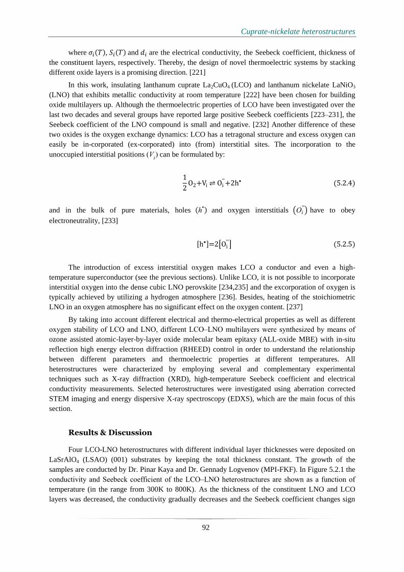
Cuprate-nickelate heterostructures
92
where 𝜎𝑖(𝑇), 𝑆𝑖(𝑇) and 𝑑𝑖 are the electrical conductivity, the Seebeck coefficient, thickness of
the constituent layers, respectively. Thereby, the design of novel thermoelectric systems by stacking
different oxide layers is a promising direction. [221]
In this work, insulating lanthanum cuprate La2CuO4 (LCO) and lanthanum nickelate LaNiO3
(LNO) that exhibits metallic conductivity at room temperature [222] have been chosen for building
oxide multilayers up. Although the thermoelectric properties of LCO have been investigated over the
last two decades and several groups have reported large positive Seebeck coefficients [223–231], the
Seebeck coefficient of the LNO compound is small and negative. [232] Another difference of these
two oxides is the oxygen exchange dynamics: LCO has a tetragonal structure and excess oxygen can
easily be in-corporated (ex-corporated) into (from) interstitial sites. The incorporation to the
unoccupied interstitial positions (Vi) can be formulated by:
1
2O2+Vi ⇌ Oi
''+2h• (5.2.4)
and in the bulk of pure materials, holes (h•) and oxygen interstitials (Oi
'') have to obey
electroneutrality, [233]
[h•]=2[Oi''] (5.2.5)
The introduction of excess interstitial oxygen makes LCO a conductor and even a high-
temperature superconductor (see the previous sections). Unlike LCO, it is not possible to incorporate
interstitial oxygen into the dense cubic LNO perovskite [234,235] and the excorporation of oxygen is
typically achieved by utilizing a hydrogen atmosphere [236]. Besides, heating of the stoichiometric
LNO in an oxygen atmosphere has no significant effect on the oxygen content. [237]
By taking into account different electrical and thermo-electrical properties as well as different
oxygen stability of LCO and LNO, different LCO‒LNO multilayers were synthesized by means of
ozone assisted atomic-layer-by-layer oxide molecular beam epitaxy (ALL-oxide MBE) with in-situ
reflection high energy electron diffraction (RHEED) control in order to understand the relationship
between different parameters and thermoelectric properties at different temperatures. All
heterostructures were characterized by employing several and complementary experimental
techniques such as X-ray diffraction (XRD), high-temperature Seebeck coefficient and electrical
conductivity measurements. Selected heterostructures were investigated using aberration corrected
STEM imaging and energy dispersive X-ray spectroscopy (EDXS), which are the main focus of this
section.
Results & Discussion
Four LCO-LNO heterostructures with different individual layer thicknesses were deposited on
LaSrAlO4 (LSAO) (001) substrates by keeping the total thickness constant. The growth of the
samples are conducted by Dr. Pinar Kaya and Dr. Gennady Logvenov (MPI-FKF). In Figure 5.2.1 the
conductivity and Seebeck coefficient of the LCO‒LNO heterostructures are shown as a function of
temperature (in the range from 300K to 800K). As the thickness of the constituent LNO and LCO
layers was decreased, the conductivity gradually decreases and the Seebeck coefficient changes sign

Cuprate-nickelate heterostructures
93
from negative to positive. In addition, both heterostructures exhibit a non-monotonic temperature
behavior for (T) and S(T) in characteristic temperature regions, which becomes apparent as the
thickness of LCO and LNO layer decreases. A similar temperature dependence was observed in the
single LCO layers, while this is not the case for a single layer LNO suggesting that LCO is
responsible for this behavior. [238]
Figure 5.2.1. a) Electrical conductivity and b) Seebeck coefficient of superlattices with different
individual layer thicknesses, as a function of temperature. Reproduced from Kaya et al. [238]
For further evaluation of the thickness and temperature dependencies of the electrical
conductivity and Seebeck coefficients, atomically-resolved STEM investigations of the samples are
performed in order to reveal possible interface effects such as cationic intermixing. For STEM
investigations I focus on two “end-members” of the sample set: One sample is composed of thicker
LCO and LNO layers (i.e. thick-layered; total thickness (u.c.) = 4 x (8xLNO/6xLCO)); the other one
has thinner LCO and LNO layers (i.e. thin-layered; total thickness (u.c.) =16 x (2xLNO/1.5xLCO)),
where the total thickness of the epitaxial film is constant. XRD patterns, STEM-HAADF images, and
EDXS line scan profiles of these two samples are presented in Figures 5.2.2 and 5.2.3. One can notice
the high-quality epitaxial relationship between the substrate and both LCO‒LNO heterostructures.
Corresponding superlattice (SL) peaks (Figure 5.2.2c), and sharp interfaces (Figures 5.2.2b,d), can be
recognized in the thick-layered sample, while the thin-layered sample shows strong chemical
intermixing through the film (Figures 5.2.3b,d) and also less pronounced SL peaks (Figure 5.2.3c).
Moreover, one can see in the HAADF image inset in Figure 5.2.3b for the thin-layered sample that
LNO adopts the nominal 113 cubic structure only in the very first layers, while the rest of the sample
exhibits the 214-tetragonal structure, in which intermixing of Cu and Ni atoms is spread through
almost the entire film.

Cuprate-nickelate heterostructures
94
Figure 5.2.2. a), b) and c) low, intermediate and high-magnification HAADF images of the thick-
layered sample grown on LSAO substrate, respectively. d) XRD pattern of the sample and e) EDXS
line scan profiles of Ni (red) and Cu (blue) along the green arrow in (b) and (c). Reproduced from
Kaya et al. [238].
In a previous study of LCO‒LNO SLs grown on LSAT (001) substrates, the 113-LNO structure
was maintained throughout the structure, and the intermixing was much more limited. [239] However,
the heterostructures grown on LSAO substrates indicates almost complete transformation to the 214-
phase after the first LNO (113) layers with strong Cu-Ni intermixing in thin-layered sample (Figure
5.2.2). Thus, a substitutional solid solution of La2(Cu,Ni)O4 with 214 crystal structure was formed
during the growth of the thin-layered heterostructure, which is also supported by the XRD
measurements employed before and after the thermal cycling indicating no structural and/or phase
change. [238] Therefore, for the thin-layered SL (i.e. 16 x (2xLNO/1.5xLCO)), the parallel slab
model ‒ using the data of LCO and LNO single phase films with the corresponding thicknesses ‒ is
not applicable due to the strong Cu‒Ni intermixing, where the sign change of the Seebeck coefficient
from negative to positive is present in LCO‒LNO heterostructures with very thin LCO and LNO
layers (as explained by a substitutional solid solution [240,241]). Nevertheless, the parallel slab model
was applied for the thick-layered SL, to further evaluate the contributions of different layers, where
the interfaces are sharper. For that, the electrical conductivity and the Seebeck coefficient of the
individual LCO and LNO layers with related thicknesses were used, and the model yields a good
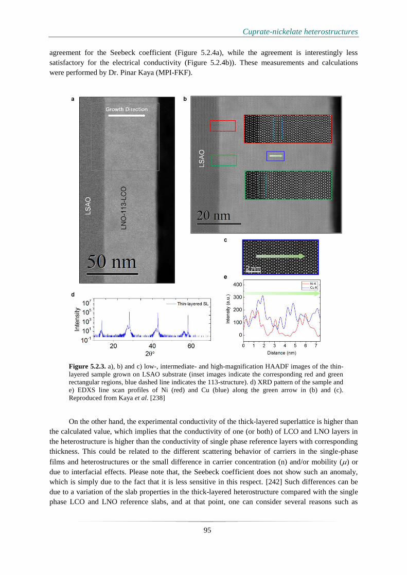
Cuprate-nickelate heterostructures
95
agreement for the Seebeck coefficient (Figure 5.2.4a), while the agreement is interestingly less
satisfactory for the electrical conductivity (Figure 5.2.4b)). These measurements and calculations
were performed by Dr. Pinar Kaya (MPI-FKF).
Figure 5.2.3. a), b) and c) low-, intermediate- and high-magnification HAADF images of the thin-
layered sample grown on LSAO substrate (inset images indicate the corresponding red and green
rectangular regions, blue dashed line indicates the 113-structure). d) XRD pattern of the sample and
e) EDXS line scan profiles of Ni (red) and Cu (blue) along the green arrow in (b) and (c).
Reproduced from Kaya et al. [238]
On the other hand, the experimental conductivity of the thick-layered superlattice is higher than
the calculated value, which implies that the conductivity of one (or both) of LCO and LNO layers in
the heterostructure is higher than the conductivity of single phase reference layers with corresponding
thickness. This could be related to the different scattering behavior of carriers in the single-phase
films and heterostructures or the small difference in carrier concentration (n) and/or mobility () or
due to interfacial effects. Please note that, the Seebeck coefficient does not show such an anomaly,
which is simply due to the fact that it is less sensitive in this respect. [242] Such differences can be
due to a variation of the slab properties in the thick-layered heterostructure compared with the single
phase LCO and LNO reference slabs, and at that point, one can consider several reasons such as

Cuprate-nickelate heterostructures
96
chemical intermixing, space charge effect, effect of epitaxial strain and different oxygen
concentration and/or different scattering in the heterostructure compared with the reference layers. A
specific local interfacial contribution cannot be the main reason, because that would require very high
conductivity.
Figure 5.2.4. Seebeck coefficient (blue) and electrical conductivity (black) of superlattices with
thick constituent layer as a function of temperature obtained experimentally and calculated by
applying the parallel slab model. Reproduced from Kaya et al. [238]
Summary and conclusions
In this section, the relationship between constituent layer thickness and the thermoelectric
properties of LCO‒LNO multilayers grown by ozone-assisted MBE are studied in the temperature
range from 300 to 800 K. It is demonstrated that, in LCO‒LNO heterostructures with relatively thick
LCO and LNO layers the thermoelectric properties are mainly dominated by the more conducting
LNO layers and can be described by the parallel slab model. In the multilayers, a sign change of the
Seebeck coefficient was observed depending on the thickness of the constituting layers: As they get
thinner the Seebeck coefficient changes from negative to positive numbers, which is explained by the
intermixing of Cu and Ni atoms resulting in a p-type Cu-rich substitutional solid solution of the form
La2(Cu1‒xNix)O4+δ and by the formation of the 214 structure, when the individual layers become very
thin. Moreover, the non-monotonic temperature dependencies of σ(T) and S(T) in LNO‒LCO
heterostructures, which are attributed to the oxygen exchange dynamics in the 214 crystal structure of
the LCO layers, revealed that the oxygen stoichiometry can decisively modify the electrical
conductivity and the Seebeck coefficient of the constituent oxide layers.
This study demonstrates that the design of artificial thermoelectric materials is possible by
stacking oxide layers, but in order to optimize the functional thermoelectric properties one needs to
pay attention to: (i) Possible formation of solid solutions in heterostructures, especially if the
constituent layer thickness is very small. (ii) The oxygen stoichiometry owing to the comparatively
large temperature range targeted for applications, where both kinetic and thermodynamic aspects are
crucial for a description of the thermoelectric properties.
Cuprate-manganite heterostructures
97
6. Cuprate-manganite
heterostructures
Abstract
The interfaces of epitaxial complex oxide systems inducing intriguing
functionalities, which are dominated by the local properties at the contacts of
heterojunctions, require atomic resolution identification. In this chapter, structural and
chemical properties of superconducting-ferromagnetic, i.e. cuprate-manganite,
heteroepitaxial interfaces probed with comprehensive aberration-corrected STEM
techniques is presented. The investigations demonstrate that Sr redistribution in 113-
LaMnO3 and 214-La2CuO4 phases is different: Sr is strongly redistributed in 113-
manganite heterostructure floating over the later-deposited La-O layers. This trend in
113-LaMnO3 is very distinct from that in 214-La2CuO4 phases. Such distribution not
only affects the sharpness of the interfaces but also influences the local octahedral
distortions and the physical properties, correlatively.

Cuprate-manganite heterostructures
98
6.1 Anomalous Sr distribution at La2CuO4/LaMnO3
heterostructures
Introduction
The phenomena occurring at oxide heterostructure interfaces can be primarily tailored by the
choice of the constituents. However, the key factor dominating the interface functionalities is the
control of interface sharpness, which can be identified by the order of cationic intermixing, i.e.
elemental redistribution. Therefore, examining the interfacial structure and chemistry is vital for
correlating the physical properties. For instance, in La2CuO4 (LCO) based, i.e. 214-type, high-
temperature superconducting (HTSC) interfaces, the importance of dopant distribution in overdoped-
undoped LCO bilayer systems [79,89] and the mechanism of cationic distribution in 2D-doped LCO
systems [84] for iso-structural cuprate-cuprate interfaces have been reported recently (see chapter 4).
In these studies, aberration-corrected [104] scanning transmission electron microscopy (STEM) has
provided local-probing techniques such as high-angle annular dark-field (HAADF) imaging [105],
annular bright-field (ABF) imaging and electron energy-loss spectroscopy (EELS) with subatomic
precision. [89]
In addition to the iso-structural systems, hetero-structural systems exhibit intriguing properties
as well. One of the most important example of such heteroepitaxial systems is the interfacial contact
of HTSC (Y,Ca)Ba2Cu3O7 (YBCO) and a ferromagnetic La0.67Ca0.33MnO3 (LCMO), where orbital
reconstruction and charge transfer take place at the interface. [243] Recently, the antiferromagnetic
coupling between Cu and Mn spins was also demonstrated in a similar heterostructure with another
type of cuprate, (La,Sr)2CuO4, and considered as a “ubiquitous” behavior of cuprate/manganite
interfaces. [244] The charge transfer within the layers can be tuned via controlling the compositions
of the superlattices with sub-unit cell precision [245] and it is natural to connect the local
lattice/chemical structure to such physical phenomena.
To understand the mechanisms of the formation of hetero-structural interfaces and their
influence on the functionalities, cuprate-manganite superlattices with different cuprate layer
thicknesses are fabricated by an ALL-oxide MBE system, that enables precise control (i.e. atomic
layer level) of the film stoichiometry. In order to realize the cationic distribution and related local
distortions at the interfaces of different phases, i.e. 113- and 214-phases, comprehensive aberration-
corrected STEM techniques are applied. The Sr distributions in 113-manganite and 214-LCO phases
are found to be dissimilar. In particular, Sr-O layer of SrMnO3 deposited on top of 214-cuprates
strongly segregates in the growth direction, floating through the LaMnO3 layers deposited on top. The
Sr-O layer (i.e. δ-doping) of LaSrCuO4 deposited on top of 113 manganites shows different elemental
distribution and chemical sharpness compared to the conventional case.
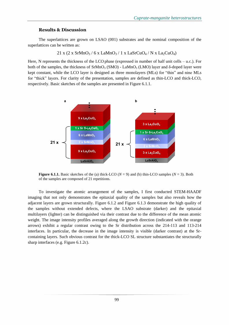
Cuprate-manganite heterostructures
99
Results & Discussion
The superlattices are grown on LSAO (001) substrates and the nominal composition of the
superlattices can be written as:
21 x (2 x SrMnO3 / 6 x LaMnO3 / 1 x LaSrCuO4 / N x La2CuO4)
Here, N represents the thickness of the LCO phase (expressed in number of half unit cells – u.c.). For
both of the samples, the thickness of SrMnO3 (SMO) - LaMnO3 (LMO) layer and δ-doped layer were
kept constant, while the LCO layer is designed as three monolayers (MLs) for “thin” and nine MLs
for “thick” layers. For clarity of the presentation, samples are defined as thin-LCO and thick-LCO,
respectively. Basic sketches of the samples are presented in Figure 6.1.1.
Figure 6.1.1. Basic sketches of the (a) thick-LCO (N = 9) and (b) thin-LCO samples (N = 3). Both
of the samples are composed of 21 repetitions.
To investigate the atomic arrangement of the samples, I first conducted STEM-HAADF
imaging that not only demonstrates the epitaxial quality of the samples but also reveals how the
adjacent layers are grown structurally. Figure 6.1.2 and Figure 6.1.3 demonstrate the high quality of
the samples without extended defects, where the LSAO substrate (darker) and the epitaxial
multilayers (lighter) can be distinguished via their contrast due to the difference of the mean atomic
weight. The image intensity profiles averaged along the growth direction (indicated with the orange
arrows) exhibit a regular contrast owing to the Sr distribution across the 214-113 and 113-214
interfaces. In particular, the decrease in the image intensity is visible (darker contrast) at the Sr-
containing layers. Such obvious contrast for the thick-LCO SL structure substantiates the structurally
sharp interfaces (e.g. Figure 6.1.2c).

Cuprate-manganite heterostructures
100
Figure 6.1.2. (a) Low magnification STEM-HAADF images of the thick-LCO SL demonstrate the
high-quality epitaxy. (b) STEM-HAADF image intensity profile along the orange arrow in Fig. 1a,
averaged along the perpendicular direction. The image intensity indicates the periodicity of the
contrast related to the Sr distribution at the interfaces. (c) High-magnification image of the area
highlighted by the red rectangle in (a) confirming the structurally coherent 214-113 and 113-214
interfaces.
Figure 6.1.3. (a) Low magnification STEM-HAADF images of the thin-LCO SL demonstrate the
high-quality epitaxy. (b) STEM-HAADF image intensity profile along the orange arrow in Fig. 1a,
averaged along the perpendicular direction. The image intensity indicates the periodicity of the
contrast related to the Sr distribution at the interfaces. (c) High-magnification image of the area
highlighted by the red rectangle in (a) confirming the structurally coherent 214-113 and 113-214
interfaces.

Cuprate-manganite heterostructures
101
After revealing the structurally coherent interfaces, atomically-resolved STEM-EELS
investigations are performed in order to evaluate the elemental intermixing (i.e. the chemical
sharpness) at the interfaces. Figure 6.1.4a-d show atomic resolution maps of Sr (blue), La (green), Mn
(red), Cu (cyan) and the overlay (RGB) of these elements as obtained via STEM-EELS, respectively.
The La and Sr substitution in the manganite phase (Figure 6.1.4a,b) and the eight-monolayer-thick
Mn distribution (Figure 6.1.4c) are revealed. Here, the substitution of La3+
with Sr2+
(divalent
alkaline-earth metal), which provides potential charge carriers for electrical conductivity [246], results
in a mixed valance of Mn3+
and Mn4+
, where the ions exchange the carriers via O-2p orbitals as
explained by the double-exchange mechanism. [72,247,8] Moreover, as a consequence of such atomic
intermixing emerging at the SMO-LMO interface, the expected electronic structure is a mixture of
t2g3eg
1 and t2g
3eg
0 configurations. EELS results clearly indicate that the elemental intermixing is mostly
confined to 2-3 UC (Figure 6.1.4). That is in a good agreement with the polarized neutron
reflectometry (PNR) measurements demonstrating the magnetic profile of the individual layers as
employed for identical systems. [245]
Figure 6.1.4. The atomically resolved elemental maps obtained via EELS spectroscopy, are
displayed in panels a), b), c) and d) for Sr (blue), La (green), Mn (red), and Cu (cyan) respectively.
e) displays the overlay of the three elements. f) shows the Sr distribution profiles across both
interfaces. The linear distortion in the experimental spectrum image is corrected via STEM SI Warp
software [129] for the Sr profile plot in (f). Please note that, for clarity, the nominal SrMnO3 and Sr
δ-doped La2CuO4 layers are shaded light-blue.

Cuprate-manganite heterostructures
102
Furthermore, in the 113-phase (i.e. SMO-LMO contact) the increased Sr concentration in
growth direction is noteworthy, in which the position of the Sr-O layers are majorly deviated from the
position they were nominally deposited (Figure 6.1.4). This is an example of Sr segregation towards
the surface triggered by the locally induced in-plane strain via La and Sr substitution. In particular,
the larger Sr atoms [96] – compared to La – are re-arranged in the structure, in order to relieve the
strain and the system is relaxed via the mild modification (i.e. segregation) instead of any defect
formation, as high-epitaxial quality is evidenced via STEM-HAADF imaging (Figure 6.1.2, 6.1.3).
This behavior is similar to the Ba segregation in epitaxial La2CuO4-based systems. [89] The
difference in the present case is the sudden stop of Sr distribution after 4 MLs. The importance of the
interface sharpness (smoothness) for SMO-LMO superlattices, which directly affects the
enhancement (reduction) of the ferromagnetic moment at the interfaces, have been reported.
[176,248] But our observation is slightly different from that of the SMO-LMO interfaces reported
before. [249]. Such difference could be due to the compressive strain induced by the LSAO substrate
and LCO interlayers, which maximizes the effect of the local strain. These findings suggest that the
interface sharpness can be further tuned via heteroepitaxial contacts, which influences the magnetic
profiles.
Simple segregation is not enough to explain the obvious presence of La-rich (or Sr-deficient)
A–O column detected on the first nominal SMO layer and the sudden termination of the SrO
segregation. In addition to the HAADF image contrast (Figure 6.1.3), STEM-EELS analyses clearly
evidence the La-rich first layer and the Sr segregation in growth direction as well as the A- and B-
type interface formation [244] at two interfaces (Figure 6.1.4). Here, one can suggest that the local
charge of the layers (polar and unipolar layers) plays a role in this case. The negatively charged
CuO2 layers attract the positively charged LaO layers and the SrO layers are pushed upwards.
[139] The abrupt termination of the SrO segregation takes place after the charge is compensated by
the LaO layers. Therefore, one can speculate that in addition to the elastic strain energy induced by
the size difference of La3+
and Sr2+
, the local charge difference triggered by La3+
and Sr2+
substitution
plays role in this picture as well. Nevertheless, these interfaces need further examination for detailed
evaluation of the mechanism lays behind.
On the other hand, the elemental intermixing on the next interface (i.e. 113-214 interface;
manganite-cuprate) shows an interesting contrast at the SMO-LMO interface. The Sr distribution in
the system clearly demonstrates the dissimilarity of Sr profiles in two different phases (Figure 6.1.4).
In particular, the 2D-doping of Sr in the La2CuO4 phase exhibits an asymmetric profile, as reported in
previous studies. [55,84] However, our results demonstrate different redistribution lengths in both
substrate and growth directions. The distribution in the growth and substrate directions are measured
around 1.3 nm (~2 uc) and ~0.65 nm (~ 1 uc), respectively, which gives rise to a sharper interface
similar to that of Sr and Ca-doped M-I bilayer structures reported recently. [79] Such difference can
be ascribed to the epitaxial strain from LaMnO3, since the growth conditions (~600-650 °C, 3x10⁻⁵
Torr) are the same as for the previous 2D-doping case [84], and therefore, cannot induce different
growth kinetics and one can refer to an indirect influence. Nominally, when the compressive strain is
induced via the LSAO substrate, 2D-doping in related La2CuO4-based systems demonstrate
superconducting transition temperatures over 35K [55]. However, in this case, the superconducting
transition temperatures are around 25 K instead [245].

Cuprate-manganite heterostructures
103
The octahedral distortions at oxide heterostructure interfaces are crucially affected by local
elemental distribution [89] and have a direct link to the magnetic [153] and electronic [16,79]
properties. Therefore, I further conducted STEM-ABF and STEM-HAADF imaging (Figure 6.1.5)
that are appropriate methods to quantify the local distortions when combined. Basal (in-plane) and
apical (out-of-plane) O–O and La–La interatomic distortions are measured on ABF (Figure 6.1.5a)
and HAADF (Figure 6.1.5c) images, respectively. Measured distances versus the number of Cu-O (or
Mn-O) layers, which are visible in this particular projection, are displayed in Figure 6.1.5b,d.
Figure 6.1.5. a) STEM-ABF image displaying all atomic column positions including O-column
positions. b) O–O interatomic distances along basal (in-plane) and apical (out-of-plane) directions
exhibit the variations across the interfaces. c) The STEM-HAADF image displays the coherent
interfaces and the weaker contrast in the Sr-rich region (1-2 MLs). d) La–La interatomic distances
along basal (in-plane) and apical (out-of-plane) directions exhibit the variations across the
interfaces. The blue and orange arrows on the images indicate the nominal 214-113 and 113-214
interfaces. The apical and basal distances are indicated with straight and dashed lines, respectively.
The error bars give the 95% confidence interval (corresponding to 2 times the standard error) of the
average of 14 unit cells of the perovskite lattice along the basal (in-plane) direction.
First of all, the basal (in-plane) interatomic distances are about the same along the layers and
are measured around 3.90 Å for both of the O–O and La–La basal (in-plane) distances (Figures
6.1.5b,d). This is an indication of the compressive in-plane epitaxial strain induced by the substrate.
Regarding the O–O interatomic distance, the larger distances measured in cuprate layers (~ 4.30 ±
0.05 Å) compared to manganite layers, which saturates around 3.90Å, show an abrupt decrease after
the 4th layer. Interesting findings stand out when both Sr-containing interfaces are taken into
consideration and compared. In particular, the abrupt increase of O–O distance at the last unit cell of
the manganite layer (i.e. 12th layer) is noteworthy. Such increase may be related to the space-charge
region formed next to the nominal interface. [55] Moreover, the gradual increase of O–O interatomic
(apical) distances starting from 13th layer is an example of an anti-Jahn–Teller distortion as observed
in homogenously-doped La2CuO4 systems. [33] This gradual increase instead of an abrupt change is
Cuprate-manganite heterostructures
104
due to the longer Sr tail in growth direction. The measurements also showed that, instead of a sharp
transition, the apical O–O distances shows a gradual increase just after the 113-214 interface, which
suggests that the 214-113 interface is sharper than the 113-214 interface.
Another point to consider is the local effect of substituting La3+
cations with Sr2+
cations, for
which the measurement of La-La apical interatomic distances provides direct information (Figure
6.1.5d). In particular, while in the first LCO layer the La–La distances are constant (~3.61 Å), in the
last Sr-containing unit cell of SMO-LMO contact (i.e. 7th layer), the distance is measured as
3.82±0.04 Å. This is followed by the LMO layer with a La–La distance measured as 3.93±0.04 Å
which demonstrates that the presence of a larger (i.e. Sr2+
) cation in the system suppresses the La–La
interatomic distances. Besides, on the 113-214 interface, (again, similar to O–O distances) a smooth
transition of the interatomic distances is observed, and this can be explained via the Sr redistribution –
with a decay length of 1.3 nm – in growth direction after the nominal interface.
Conclusion
In conclusion, in order to examine the interface formation and the structural and chemical
sharpness at the interfaces, ALL-oxide MBE grown lanthanum cuprate-lanthanum manganite
heterostructures are probed utilizing comprehensive STEM techniques. The investigations
demonstrate the differences of Sr profiles together with the interrelated local lattice deformations that
affect the interface sharpness. The observations not only substantiate the tunability of Sr redistribution
at oxide heterostructures interfaces via employing different phases but also indicate that sharper
interfaces can be obtained via 113-214 contacts. It is further suggested that hetero-epitaxial contacts
can be used as a tool to tailor the sharpness of the interfaces, which may lead to tune the physical
properties.

Nickelate-based oxide heterostructures
105
7. Nickelate-based oxide
heterostructures
Abstract
In this chapter, state of the art scanning transmission electron microscopy is
used to investigate the crystallographic reorientation of NdNiO3 grown on [011]-
oriented NdGaO3 substrates. A comprehensive analysis of the microscopy data relates
the observed reorientation from the [011]-phase (α-phase) to the [101]-phase (β-
phase) to the specific [011]-directionality of the substrate induced epitaxial strain,
which can be understood within the framework of DFT+U calculations. In addition,
the calculations reveal enhanced NiO6 octahedral breathing distortions for tensile
strained β-phases of NdNiO3, which can rationalize recent reports of enhanced metal-
insulator transition temperatures in similar NdNiO3-NdGaO3 heterostructures. The
observation of a crystallographic reorientation within an epitaxial thin film suggests a
new route to tune material properties in heterostructures for future applications in
functional devices.

Nickelate-based oxide heterostructures
106
7.1 Structural reconstruction in NdNiO3 thin films
Introduction
Over the last years, technical advances in the synthesis of epitaxial thin films have allowed to
stabilize materials of extraordinary stoichiometry and to tailor their properties in an unprecedented
fashion. [1,2,4,250] Along these lines, in addition to molecular beam epitaxy (see previous chapters),
ablation techniques such as pulsed laser deposition (PLD) [14,15] enable the epitaxial combination of
transition metal oxides (TMOs) and other material classes in artificial multilayer systems. In this
unique environment, where distinct electronic, magnetic, and orbital correlations can be brought
together, novel phenomena, which are not present in the constituents alone, can emerge. [3,4]
Prominent examples for such phenomena are induced electronic and magnetic phase transitions [251],
orbital reconstructions [6], and interface superconductivity. [9,10]
A profound understanding of the mechanisms leading to the occurrence of novel phases is of
utmost importance and enables their controlled appearance, as required for their exploitation in future
functional devices. One approach to gain deeper insights explores the materials' response to a
variation of external parameters like strain [86,252], doping [79], or electric [253] and magnetic
fields. In the case of perovskite TMOs, it was reported that, in addition to the aforementioned
parameters, the oxygen octahedral network at the interfaces plays a key role. [33,254–256] The
peculiar interfacial epitaxial connection of the substrate or a buffer layer and the deposited film
material imposes structural constraints that allow to widely tune emergent material properties, due to
the close relation between crystal lattice and electronic, magnetic, and orbital correlations.
In more detail, it was found by means of scanning transmission electron microscopy (STEM)
[152,153] that the octahedral coupling between TMO perovskite materials does not only transfer
epitaxial strain but also octahedral rotations of the underlying substrate or buffer layer, yielding a
modification of properties such as the magnetic anisotropy. [153] In general, the material-substrate
relation in the closest interface is of one-to-one type, i.e. the material adopts the in-plane lattice
parameters, the octahedral tilt pattern, and the crystallographic orientation of the substrate, while with
increasing film thickness these parameters relax towards the bulk values of the material. For particular
material combinations, however, epitaxial films can adopt the substrate’s tilt pattern even on length
scales of several tens of nm away from the interface. [257] In case of matching crystallographic
symmetries of substrate and epitaxially deposited film, the film material's unit cells are expected to
coincide in their orientation with the substrate, i.e. the substrate orientation determines the orientation
of the film.
In this work, spherical aberration (Cs) corrected [104] STEM is used to investigate
heterostructures of the perovskite NdNiO3 (NNO) and the paramagnetic insulator NdGaO3 (NGO).
TMO heterostructures containing RNiO3 (R = rare earth element) have recently attracted wide-spread
interest following theoretical predictions of possible high-Tc superconductivity. [58] In the octahedral
environment of the RNiO3 perovskite structure the Ni3+
ions are coordinated to six O ions, formally
providing Ni with 3d7 (t2g
6 eg
1) configuration. The degree of the Ni‒O‒Ni bond angle distortion
determines the transition temperature for the phase transition from the high temperature paramagnetic
metallic state to the insulating and antiferromagnetic ground state, occurring for all members of the
RNiO3 family, except for R = La. [258] Moreover, the metal-insulator transition coincides with a
structural phase transition from orthorhombic to monoclinic symmetry characterized by a octahedral
Nickelate-based oxide heterostructures
107
breathing distortion yielding two inequivalent Ni sites Ni3+δ
and Ni3-δ
. For the prototypical rare-earth
nickelate NNO, which in a thin film undergoes a metal-insulator and paramagnetic-antiferromagnetic
transition at ~150 K [259], it was shown that the metal-insulator transition temperature is significantly
elevated to ~335 K, when NNO films are epitaxially grown on [101] oriented (β-phase) NGO
substrates. [260] It was speculated that the specific lattice matching condition between the
orthorhombic NNO and NGO for [101] orientation might yield a transfer of the NGO octahedral
rotations (i.e. the Ga‒O‒Ga bond angles) to the NNO octahedral rotations (i.e. the Ni‒O‒Ni bond
angles) not only in proximity to the substrate-film interface, but across the whole thickness of the
studied 17 nm thick NNO film. Such an alternation of the Ni‒O‒Ni bond angle distortions would tune
the hopping integral between the O 2p and Ni 3d orbitals and therewith increase the effective
electronic bandwidth of the system, which could explain the elevated metal-insulator transition
temperature.
Here, a similar material system is investigated, i.e. an NNO thin film epitaxially grown on a
[011]-oriented (α-phase) NGO substrate. From high-angle annular dark-field (HAADF) [105] and
annular bright-field (ABF) [106,107] imaging it is found that the NNO film reorients after a few unit
cells from [011] to [101] orientation (α to β-phase), as opposed to maintaining the [011] orientation
given by the substrate. Such reorientation is revealed in both, the local Nd- and Ni-site displacements
and the alteration of Ni‒O‒Ni bond angles across the interface region and the film. To rationalize the
unexpected emergence of the β-phase on an α-phase substrate, DFT+U calculations are employed to
simulate epitaxial strain along different crystallographic directions, reproducing the observed phase
reorientation and predicting the absence of reorientation for growth on β-phase substrates. Further,
from the ABF analyses, the previously suggested transfer of the NGO octahedral rotations across the
full thickness of an NNO film is not confirmed, but instead a relaxation of the NNO octahedral
rotations (i.e. the Ni‒O‒Ni bond angles) to bulk-like values after a few unit cells from the substrate-
film interface is revealed. Furthermore, the DFT+U calculations show that in the tensile strained β-
phase the monoclinic breathing distortion can be enhanced. Such behavior correlates with an elevated
metal-insulator transition temperature, and hence is consistent with the reported increase of the
transition temperature in ref. [260].
Results
Several NNO samples were grown by PLD by G. Cristiani and Dr. G. Logvenov (MPI-FKF).
Here, the focus is on an NNO thin film with a thickness of 11.4 nm grown on a NGO substrate
(Figure 7.1.1a) with [011] orientation (α-phase), i.e. the NGO substrate surface corresponds to a (011)
plane (Figure 7.1.1b). Both, bulk NNO and NGO exhibit the orthorhombic space group Pbnm at
room-temperature. The lattice parameters are a = 5.428 Å, b = 5.498 Å, and c = 7.709 Å in the case of
NGO [261] and a = 5.387 Å, b = 5.383 Å, and c = 7.610 Å in the case of NNO. [262] In this work, the
main focus is on the α and β substrate orientations, corresponding to the cuts perpendicular to the
(111) body diagonal of the pseudocubic unit cell. Note that, while in the simplified pseudocubic
reference frame all body diagonals are equivalent, the (011) and (101) planes (α-and β-planes) of the
orthorhombic Pbnm unit cell of NNO and NGO are not (Figure 7.1.1a). In a typical epitaxial film
growth scenario involving a perovskite TMO material deposited on a compatible oxide substrate, the
thin film orients in congruence with the substrate. Moreover, the epitaxial film-substrate relation is
expected to be particularly robust for substrates with surfaces perpendicular to one of the pseudocubic

Nickelate-based oxide heterostructures
108
body diagonals (e.g. α- and β-orientation), due to the 3-fold interconnectivity of the octahedral
network across an epitaxial interface (Figure 7.1.1b).
Figure 7.1.1. (a) Depiction of the NdNiO3 unit cell (black lines) in orthorhombic space group Pbnm.
The planes corresponding to the [011] –and [101]– cut (α- and β-cut) are indicated in blue and red,
respectively. For clarity only one NiO6 octahedron (gray) is superimposed to the unit cell. (b)
Schematic of the interconnectivity of the octahedral network across the epitaxial NdNiO3–NdGaO3
interface. One NiO6 octahedron (gray) is shown in proximity to the α-cut NdGaO3 substrate surface
(blue). Each interfacial NdNiO3 octahedron connects to three NdGaO3 octahedra (black arrows).
(c)-(f) Illustration of the in-plane epitaxial strain induced to the NdNiO3 unit cell (gray rectangular)
by an underlying NdGaO3 substrate (orange rectangular) for different combinations of α -and β-cuts.
The indicated in-plane directions of the projected unit cells lie within the α- and β-planes. Unit cell
dimensions are exaggerated for clarity. The numbers are the strain magnitudes along these
directions calculated as explained in the text. Note that the effective strains for the growth modes α
on α (c) and β on α (f) are closely similar.

Nickelate-based oxide heterostructures
109
The larger NGO unit cell dimensions yield tensile in-plane strain for all epitaxial combinations
of the NNO unit cell to an NGO substrate. The magnitude of the epitaxial strain along the main in-
plane directions depends strongly on the combination of orientations of the two materials. The
schematics illustrating the epitaxial film-substrate relation are depicted in Figure 7.1.1c-f with the
gray and orange rectangulars corresponding to the in-plane projections of an NNO and NGO unit cell
in α- and β-orientation, respectively. The calculated effective strain (lNGO−lNNO)/lNNO with l being the
lattice parameter along the respective main crystallographic direction, based on the material's bulk
lattice parameters at room temperature, yields ~1.3% along the [01-1] and ~0.5% strain along the
[100] direction for α-oriented NNO on α-NGO and ~0.8% along the [-101] and ~2.0% strain along
the [010] direction for β-NNO on β-NGO. The (at this point) hypothetical combination of α-NNO on
β-NGO (Figure 7.1.1e) yields a similar magnitude of strain along the in-plane directions as β-NNO on
β-NGO (Figure 7.1.1d). The same applies for β-NNO on α-NGO (Figure 7.1.1f) and α-NNO on α-
NGO (Figure 7.1.1c). As a consequence, simple strain minimization cannot explain a potential
occurrence of reconstructed phases such as α on β or β on α (Figure 7.1.1e,f).
Aberration-corrected STEM investigations provide valuable local information on structural
details and the chemical composition at oxide heterostructure interfaces. First, the crystalline quality
and the cation intermixing, particularly in the NdNiO3-NdGaO3 interface region, are examined. An
overview STEM-HAADF image of the sample together with an EDS line scan across the interface is
presented in Figure 7.1.2. The low magnification STEM-HAADF image (Figure 7.1.2a) acquired
along the [011] direction of the NNO substrate reveals the high-quality epitaxial growth of the
NdNiO3 film as well as a defect-free structure. The NNO film (light gray) and the NGO substrate
(dark gray) can be discerned by their gray-shades in the image due to the presence of a small
difference of atomic weights of Ni and Ga (ZNi = 28 and ZGa = 31) providing Z-contrast information in
HAADF imaging. [105] Complementary LAADF imaging, which exposes defects in its contrast
[109], confirms the absence of any crystallographic stacking faults in the epitaxial NNO layer on a
larger- (i.e. micrometer-) scale (see Figure 7.1.2c). The local chemical properties of the interface are
identified by atomically-resolved EDS line scans acquired across the interface as shown in Figure
7.1.2b. The scan profiles of Ni-K (gray), Ga-K (orange), and Nd-L (black) lines reveal the chemical
intermixing of Ga-Ni at the interface, which is limited to 2-3 monolayers (MLs) corresponding to
<1.5 nm along [011] direction.
After revealing the high quality of the sample, a detailed investigation of the structural
distortions and the local octahedral network at the NGO-NNO interface is conducted by STEM-
HAADF and by STEM-ABF imaging, respectively. Figure 7.1.3 shows the STEM images together
with the corresponding data analysis. The nominal interface is defined in accordance with Figure
7.1.2b and indicated by an orange line serving as a guide to the eye. The high-resolution STEM-
HAADF image (Figure 7.1.3a) not only displays the coherent interface region between NGO and
NNO but unveils two different phases in the sample: (i) the α-oriented substrate and (ii) a β-oriented
NNO film far from the substrate with a gradual reconstruction from α to β in proximity to the
interface. The presence of the α-orientation is qualitatively deduced from an overlay of a simulated
NGO crystal structure projection to the zig-zag pattern of the atomic Nd-Ga columns (left inset Figure
7.1.3a), and congruently, the β-orientation is deduced from an overlay of the NNO crystal structure
projection to the straight columns of Nd–Ni (right inset Figure 7.1.3a).

Nickelate-based oxide heterostructures
110
Figure 7.1.2. a) STEM-HAADF image of the NdNiO3 thin film with a thickness of 11.4 nm on a
[011] oriented NdGaO3 substrate. The image illustrates the high epitaxial quality and the defect-free
structure of the film. The inset is a high-resolution STEM-HAADF image of the film-substrate
interface region. b) EDS line scan profiles along the [011] growth direction indicated by the yellow
arrow presenting the chemical composition of the NdGaO3-NdNiO3 interface. The orange, black,
and gray lines correspond to the EDS intensity of the Ga K, Nd L, Ni K, and lines, respectively.
Intermixing of Ni and Ga atomic species in the interface region of ~1.5 nm is marked by the shaded
area. The interface is defined at 0 nm and the dashed line corresponds to zero intensity of the EDS.
c) STEM-LAADF image with NdNiO3 epitaxial layer indicated by the orange arrow. No structural
defects and/or structural grains can be detected, substantiating high crystalline quality. The layer on
top of NdNiO3 is the glue from the specimen preparation. The blue box represents the dimensions
of the STEM-HAADF image in (a).
This unexpected observation is indicative of a phase reconstruction and demands a quantitative
analysis of the local atomic displacements. To this end, the Nd-site displacements, in particular, the
interatomic distance variations for the out-of-plane and in-plane directions are quantified. The
detailed analyses are employed using the recently developed software Oxygen Octahedra Picker tool
[125] that provides the required precision (see Section 3.2.5). The results can be extracted from the
panel (b) and (c) displaying the out-of-plane Nd‒Nd interatomic distance (dNd-Nd) while moving away
from the interface (orange line), which is indicated here as the number of Ni–O planes. Please note
that each data point in (b) and (c) corresponds to the average of 8 atomic columns. Obviously, a
strong zig-zag behaviour evolves as a function of increasing number of Ni–O planes corresponding to
an alteration in the structure. In more detail, with the present calibration, the out-of-plane Nd–Nd
distances in the NGO substrate are determined as 2.68 ± 0.04 Å, whereas a decrease to 2.59 ± 0.02 Å
is observed in the 4th Ni‒O plane after the nominal interface. The sharp decrease is followed by a
narrow-range (5-6 MLs) with Nd‒Nd interatomic distances around dNd–Nd = 2.65 Å. Starting from the
11th Ni‒O plane, the fluctuation (or absolute difference) in dNd–Nd between the adjacent Ni‒O planes
increases and exceeds 0.016 ± 0.05 Å and saturates. Next, the in-plane Nd‒Nd interatomic distances
are considered (Figure 7.1.3c) and a constant dNd–Nd ~3.80 Å is observed. The entire Nd cation
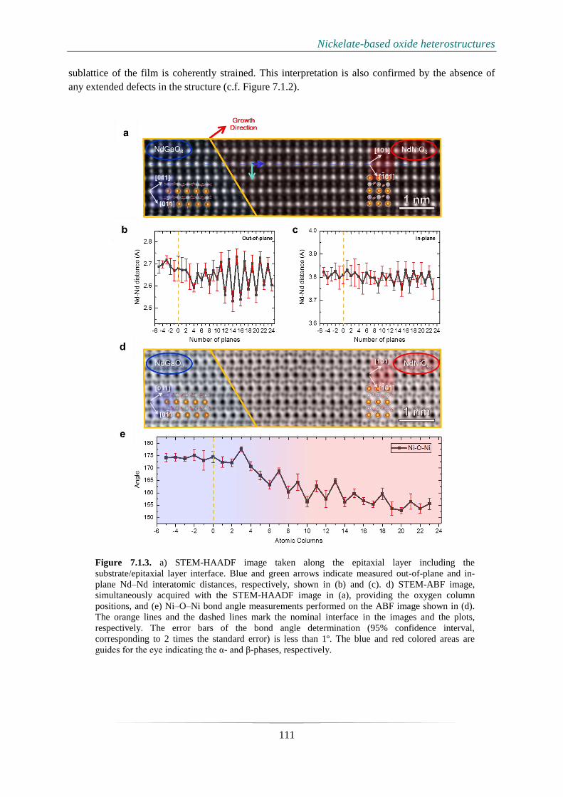
Nickelate-based oxide heterostructures
111
sublattice of the film is coherently strained. This interpretation is also confirmed by the absence of
any extended defects in the structure (c.f. Figure 7.1.2).
Figure 7.1.3. a) STEM-HAADF image taken along the epitaxial layer including the
substrate/epitaxial layer interface. Blue and green arrows indicate measured out-of-plane and in-
plane Nd–Nd interatomic distances, respectively, shown in (b) and (c). d) STEM-ABF image,
simultaneously acquired with the STEM-HAADF image in (a), providing the oxygen column
positions, and (e) Ni‒O‒Ni bond angle measurements performed on the ABF image shown in (d).
The orange lines and the dashed lines mark the nominal interface in the images and the plots,
respectively. The error bars of the bond angle determination (95% confidence interval,
corresponding to 2 times the standard error) is less than 1º. The blue and red colored areas are
guides for the eye indicating the α- and β-phases, respectively.

Nickelate-based oxide heterostructures
112
To gain deeper insights on the interface-induced reconstruction, I have used the STEM-ABF
technique, which allows imaging of light elements [105], i.e. oxygen in the present case. A STEM-
ABF image of the interface region is presented in Figure 7.1.3d with the entire set of clearly resolved
atomic columns in the structure, which are Nd‒O, Ga, Ni and O atomic columns in this projection. It
should be emphasized that the STEM-ABF image (Figure 7.1.3d) was simultaneously acquired with
the STEM-HAADF image presented in Figure 7.1.3a. Focusing on the Ni and O atomic columns, it is
obvious that the Ni‒O‒Ni pattern exhibits a clear transition from a straight line in NGO to a zig-zag
pattern in NNO away from the interface. This indicates a reorientation of the crystallographic unit cell
which can be corroborated quantitatively by measuring the bond angles between the cation sublattices
along the growth direction, namely the Ga‒O‒Ga angles in the substrate and the Ni‒O‒Ni angles in
the interfacial region and beyond. The analyses averaging 9 atomic columns (Figure 7.1.3e shows a
section of the analyzed image) give a projected Ga‒O‒Ga bond angle of 174º ± 1º. However, a
decrease of 2º of this bond angle is observed just after the interface (i.e. 7th and 8
th columns). In the
consecutive columns, the measured Ni‒O‒Ni angle indicates a transition between two different
phases. Such transformation to a β-phase is characterized by a saturation of the Ni‒O‒Ni angles
around 155º ± 1.2º. The value of ~155º extracted for the Ni‒O‒Ni angles is consistent with the bond
angle of bulk NNO, while NGO exhibits a bond angle of 153º in the corresponding projection of the β
phase.
While the presence of the reconstruction is clear from the experimental STEM data and the
detailed analyses, the mechanism behind its occurrence is not directly evident, as elucidated earlier in
the text and in the strain minimization consideration of Figure 7.1.1c–f. Therefore, DFT+U
calculations representing an α- and β-oriented NGO substrate, respectively (Figure 7.1.4) were
performed by Dr. Z. Zhong and Dr. P. Hansmann (MPI-FKF). An effective Hubbard U of 2 eV,
typical for nickelates [263,264], was employed. In Figure 7.1.4, the DFT ground-state energy
calculated as a function of the out-of-plane lattice spacing “d” for NGO α-phase and NGO β-phase are
presented, respectively. For the α-phase and β-phase calculations, the spacing d correspond to the
distance between consecutive NiO3 planes along the [011] and [101] directions, respectively. Figure
7.1.4a,b shows the energies in dependence of relative spacing d0 = d/dbulk. While the in-plane atomic
distances were fixed to the values of NGO in (011) and (101) planes, the out-of-plane distances were
allowed to vary in the calculations to account for the effect of tensile strain. For both types of
substrate cuts, i.e. α-NGO (Figure 7.1.4a) and β-NGO (Figure 7.1.4b), it is revealed that the β-NNO
phase/orientation is energetically favourable compared to the α-NNO phase/orientation within the
error bar of the experimentally obtained relative out-of-plane lattice plane spacing of 0.989 ± 0.04 Å.
This explains the experimentally observed reorientation of NdNiO3 grown on α-cut NdGaO3. For
these small values of the relative spacing d0, the calculation yields a phase (α'-phase) with α-
orientation but an altered octahedral tilt pattern, i.e. symmetry corresponding to the crystallographic
space group 𝑅3̅𝑐. While bulk LNO exhibits this space group, to the best of our knowledge, there are
no experimental reports observing NNO in space group 𝑅3̅𝑐. Since moreover the α'-phase does not
yield a global minimum, this phase is not discussed further here. Instead, the β-phase is considered in
more detail in the following. The most striking feature of the calculated NNO β-phase in the global
minima of Figure 7.1.4a,b is an enhancement of the monoclinic breathing distortion. The Ni–O bond
disproportionation for α and β-induced tensile strain (Ni–O bond lengths 1.97 Å and 1.90 Å for long
and short bond lengths, respectively) is two times larger than that of the bulk case (1.94 Å and 1.91
Å).

Nickelate-based oxide heterostructures
113
Figure 7.1.4. DFT+U ground state for different epitaxial configurations depicted in Figure 7.1.1(e-
f). (a) In-plane lattice constants of NdNiO3 are fixed at the values corresponding to the α-cut
NdGaO3, while the NdNiO3 out-of-plane lattice constant is allowed to relax, simulating the effects
of epitaxy on an α-NdGaO3 substrate surface. The NdNiO3 in-plane directions are [100] and [01-1],
and the out-plane is [011] for the α-phase calculation (blue curve). For the β-phase calculation, in-
plane directions are [010] and [-101] and the out-plane direction is [101] (red curve). The global
minimum is obtained for the β-phase calculation indicating the energetically most favorable state
that corresponds to β-phase NdNiO3 unit cells in epitaxy to the α-phase NdGaO3 substrate. This
explains the experimentally observed reorientation of NdNiO3 grown on α-cut NdGaO3.
Furthermore, the magnitude of the octahedral breathing distortion in the NdNiO3 β-phase ground
state is strongly enhanced which promotes its emergence. (b) Analogous calculation to (a), but with
NdNiO3 in-plane lattice fixed at values corresponding to β-cut NdGaO3. The global minimum is
obtained within the beta-phase calculation suggesting that no reorientation takes place in case
NdNiO3 is grown on β-cut NdGaO3.

Nickelate-based oxide heterostructures
114
Discussion
The present study is an important example for non-trivial occurrence of phase reconstructions.
As illustrated in Figure 7.1.1c-f a simple consideration of strain minimization cannot explain the
observed α-to-β phase reconstruction. By means of STEM imaging, however, several important
insights on the investigated system could be gained. First, the high quality of the NdNiO3 film in
terms of epitaxy and coherency of the crystal structure could be corroborated (Figure 7.1.2a,c). This
makes it unlikely that the observed α-to-β phase reconstruction is due to accumulation of defects and
stacking faults in the crystal lattice. Chemical intermixing at the NdGaO3–NdNiO3 interface (Figure
7.1.2b), which typically is a consequence of growth kinetics and surface segregation [79,84], was
revealed to be limited to only 1-1.5 nm in the growth direction. The transition region [265] of the
reorientation of the epitaxially connected α and β layers was, however, determined to extend up to
~10-12 ML away from the film-substrate interface (Figure 7.1.3a). This length scale is significantly
longer than the chemical intermixing region, thus interfacial disorder as a major driving mechanism
for the phase reconstruction can also be ruled out. The STEM-HAADF and STEM-ABF image
analysis gave a detailed quantification of the α and β phases, and the transition region in terms of Nd,
Ni, and O atomic positions as well as the Ni‒O‒Ni bond angles. It is shown that the Ni‒O‒Ni angle is
relaxed to the value of ~155º after the transition region implying that the NGO octahedral rotations
have not been transferred across the whole NNO film. Deeper insights on the mechanism and the
energy landscape behind the phase reconstruction were provided by the DFT+U calculations. A
global minimum in the energy landscape for the strain induced by an α-phase substrate is obtained for
NNO in β-phase orientation, rationalizing the experimentally observed phase reconstruction (Figure
7.1.4a). On the other hand, for a substrate orientation corresponding to the β-phase, also the β-phase
NNO exhibits the global minimum, i.e. no reconstruction will take place in this case (Figure 7.1.4b).
The second important result of the calculation is that the magnitude of the octahedral breathing
distortion in the NNO β-phase ground state is strongly enhanced as compared to bulk NNO. This
promotes its emergence over the α-phase and also gives an explanation for the elevated metal-
insulator transition temperature reported in ref. [260].
Conclusion
In conclusion, a comprehensive study of the structural properties and the interface chemistry of
epitaxial NdNiO3 thin films grown on NdGaO3 substrates revealed a substrate induced
crystallographic reconstruction. The atomically-resolved STEM investigations provided a unique
local probe of the samples and allowed to quantify not only structural deformations but also
modifications of the octahedral network (i.e. the alteration of Ni‒O‒Ni bond angles across the
interface region). DFT+U calculations corroborated the reconstruction found from the STEM
analysis. Thus, the present work emphasizes the importance of epitaxial strain and local structural
details at interfaces for the emergence of novel phases in thin films and heterostructures. The
methodology used can be applied to similar oxide material systems and help to improve the
understanding of strongly correlated interactions occurring at interfaces.

Epilogue
115
8. Epilogue
Abstract
This chapter gives a brief overview to the study: The aim and the motivation of
the thesis are blended with the outcomes and the conclusions obtained within the
thesis.

Epilogue
116
In this thesis, I looked for an answer to the following question: “To which extent can epitaxial
oxide heterostructures and interfaces be controlled and identified?” For this purpose, various projects
were conducted in which not only the growth of La2CuO4-based systems are performed but also the
structural and chemical identifications and octahedral distortions at the interfaces are
comprehensively investigated. Through the projects, different factors such as (i) dopant size effects,
(ii) two-dimensional doping (i.e. δ-doping), (iii) growth temperature gradient, (iv) contact of different
phases, (v) layer-thickness variations, (vi) different substrates and their influences on the interface
structures and/or on the functionalities are examined. Besides, the applications of STEM imaging and
quantification as well as the analytical techniques are extensively employed, which are associated
with the interface structures of oxide heterostructures.
It is revealed for La2CuO4 metal-insulator bilayer systems that the different cationic radii of the
dopants (Ba2+
, Sr2+
, Ca2+
) remarkably affect the superconducting mechanisms (i.e. bulk vs interface),
as a consequence of dopant redistribution near the interface. In the case of the La2-xCaxCuO4/La2CuO4
and La2-xSrxCuO4/La2CuO4 systems, the interfaces were found to be sharper, and thereby, striking
interface effects, i.e. electronic redistribution, are predominant. However, in the case of La2–
xBaxCuO4/La2CuO4, high-temperature superconductivity (HTSC) is rather ascribed to “classical”
homogeneous doping determined by wide cationic intermixing. Moreover, the dopant distribution has
a remarkable effect on the O–O distances, which are suggested to be related to different mechanisms
leading to HTSC: While the sharp interfaces are correlated with Jahn–Teller distortion, anti-Jahn–
Teller distortion is dominant for the homogeneous doping (Ba-doping) case. On the other hand, for
2D-doping of La2CuO4, it is found that the cationic dopant profiles are highly asymmetric with
different sharpnesses: Abrupt at the downward side of the interface and broadened in growth direction.
Conversely, the hole distribution, as measured by STEM-EELS, is symmetric across the interface and
is decoupled from the dopant profile at the downward interface. This indicates that hole doping is
achieved on the two sides of the Sr-doped plane by two distinct mechanisms: Heterogeneous doping
at the downward side of the interface and homogeneous doping at the upward side.
In the case of lanthanum cuprate–lanthanum nickelate multilayers, where LNO is employed as
two different phases (i.e. 214-La2-xSrxNiO4 and 113-LaNiO3), different properties, in addition to
structural considerations, are studied. For La2CuO4-La2-xSrxNiO4 contact, a chemically sharp interface
inducing a hole accumulated space-charged layer is detected by STEM-EELS analyses, while a
certain tendency for Sr to migrate from La2-xSrxNiO4 to La2CuO4 that gives rise to a ‘less’ sharp
interface. Moreover, concerning the thermoelectric properties of La2CuO4–LaNiO3 heterostructures,
the importance of the choice of the individual layer thicknesses is revealed: The thinner the individual
La2CuO4 and LaNiO3 layers, the more chemical intermixing at the interfaces occurs, which directly
influences the physical properties.
As far as the heterojunctions of La2CuO4/LaMnO3 layers are concerned, it is found that
dissimilar Sr profiles are present in cuprate and manganite phases, which lead to different interface
sharpness suggesting the tunability of Sr redistribution using oxide hetero-structural contacts.
Moreover, the quantification of local octahedral distortions indicates that 113-214 interfaces are
sharper compared to 214-113 interfaces. Concerning the NdNiO3 thin films, the realization of a
structural reorientation from the [011]-phase to the [101]-phase could be understood via DFT+U
calculations suggesting enhanced NiO6 octahedral breathing distortions.

Epilogue
117
In conclusion, the exciting output of this thesis can be summarized as the following:
(i) The choice of the dopant (size) directly affects the interface sharpness, namely, the dopant
re-distribution, local octahedral distortions and thereby the interface functionalities in
La2CuO4 based systems.
(ii) Two-dimensional doping (i.e. δ-doping) of La2CuO4 in the form of superlattices results in
different dopant distribution at both sides of the interfaces due to the growth kinetics and
correlatively induces the different superconducting mechanisms at two sides of the
interfaces.
(iii) The defect chemistry and the transfer of the species can induce space-charge regions in
both homoepitaxial (e.g. δ-doping of La2CuO4) and heteroepitaxial (e.g. La2CuO4 - La2-x
SrxNiO4 contacts) oxide systems with sharp interfaces.
(iv) The choice of the layer thickness in heterojunctions, e.g. La2CuO4-LaNiO3 contacts, is of
great importance and may result in the unintentional occurrence of different phases or
solid solutions.
(v) The dopant distribution of the same element (i.e. Sr) in different materials exhibit different
elemental distribution even at consecutive interfaces.
(vi) In NdNiO3 films, a reconstruction of the crystallographic orientation is detected when
tensile strain is imposed by a [011]-oriented NdGaO3 substrate.
In summary, in addition to the remarkable capabilities of ALL-oxide MBE system, the
feasibility of using spherical aberration corrected STEM to quantitatively describe the elemental
distribution, charge distribution and the local atomic distances in LCO-based interfaces are discussed.
Although numerous oxide heterostructures with different novel properties have been studied, this
thesis provides a comprehensive overlook to homoepitaxial and heteroepitaxial interfaces. This work
underlines that various factors affect the interface profiles and give rise to different physical
properties, although atomic-precise engineering and identification are possible.

Epilogue
118
This page intentionally left blank

Appendices
119
9. Appendices
9.1 A : List of publications
Published: During PhD
1. Y. E. Suyolcu, Y. Wang, F. Baiutti, W. Sigle, G. Cristiani, J. Maier, G. Logvenov, P. A. van
Aken, “Aberration-Corrected Scanning Transmission Electron Microscopy of La2CuO4-based
Superconducting Interfaces at the Stuttgart Center for Electron Microscopy” JEOL News,
53(1), 8-17, 2018. (Invited; Front Cover) [266]
2. Y. E. Suyolcu, Y. Wang, W. Sigle, F. Baiutti, G. Cristiani, J. Maier, G. Logvenov, P. A. van
Aken, “Octahedral Distortions at High-temperature Superconducting La2CuO4 Interfaces:
Visualizing Jahn–Teller Effects” Advanced Materials Interfaces, 4, 1700737, 2017.
(Frontispiece Cover) [89]
3. Y. E. Suyolcu, Y. Wang, F. Baiutti, A. Al-Temimy, G. Gregori, W. Sigle, G. Cristiani, J.
Maier, P. A. van Aken, G. Logvenov, “Dopant size effects on novel functionalities: High-
temperature interfacial superconductivity”, Scientific Reports, 7, 453, 2017. [79]
4. M. Hepting, R. J. Green, Z. Zhong, M. Bluschke, Y. E. Suyolcu, S. Macke, A. Frano, S.
Catalano, M. Gibert, R. Sutarto, F. He, G. Cristiani, G. Logvenov, Y. Wang, P. A. van Aken,
P. Hansmann, M. Le Tacon, J.-M. Triscone, G. A. Sawatzky, B. Keimer, E. Benckiser;
“Complex magnetic order in nickelate slabs", Nature Physics, 10, 1097–1102, 2018. [267]
5. P. Kaya, G. Gregori, F. Baiutti, P. Yordanov, Y. E. Suyolcu, G. Cristiani, F. Wrobel, E.
Benckiser, B. Keimer, P. A. van Aken, H.-U. Habermeier, G. Logvenov and J. Maier, “High
Temperature Thermoelectricity in LaNiO3-La2CuO4 Heterostructures ", ACS Appl. Mater.
Interfaces, 10(26), 22786-22792, 2018. [238]
6. F. Baiutti, G. Gregori, Y. E. Suyolcu, Y. Wang, G. Cristiani, W. Sigle, P. A. van Aken, G.
Logvenov and J. Maier; “High-temperature superconductivity at the lanthanum
cuprate/lanthanum-strontium nickelate interface”, Nanoscale, 10(18), 8712-8720, 2018. [205]
7. Y. Wang, Y. E. Suyolcu, U. Salzberger, K. Hahn, V. Srot, W. Sigle, P. A. van Aken,
“Correcting the linear and nonlinear distortions for atomically resolved STEM spectrum and
diffraction imaging”, Microscopy, 67, i114-i122, 2018. [129]
8. F. Baiutti, G. Gregori, Y. Wang, Y. E. Suyolcu, G. Cristiani, P. A. van Aken, J. Maier, G.
Logvenov, “Cationic Redistribution at Epitaxial Interfaces in Superconducting Two-
Dimensionally Doped Lanthanum Cuprate Films”, ACS Appl. Mater. Interfaces, 8, 27368-
27375, 2016. [84]
9. Y. Wang, U. Salzberger, W. Sigle, Y. E. Suyolcu, P. A. van Aken, “Oxygen Octahedra Picker:
a software tool to extract quantitative information from STEM images”, Ultramicroscopy, 168,
46-52, 2016. (Front Cover) [125]

Appendices
120
Published: Earlier Work
10. M. Korkmaz, B. Arikan, Y. E. Suyolcu, B. Aslan, U. Serincan, “Performance evaluation of
InAs/GaSb superlattice photodetector grown on GaAs substrate using AlSb interfacial misfit
array”, Semicond. Sci. Technol., 33, 035002, 2018.
11. S. Ozdemir, Y. E. Suyolcu, S. Turan, B. Aslan, “Influence of the growth conditions on the
optical and structural properties of self-assembled InAs/GaAs quantum dots for low As/In
ratio”, Applied Surface Science, 392, 817-825, 2017.
12. B. Arikan, G. Korkmaz, Y. E. Suyolcu, B. Aslan, U. Serincan, "On the crystallographic
characterization of InAs/GaSb type-II superlattices: The effect of interfaces for fixed layer
thicknesses", Thin Solid Films, 548, 288-291, 2013.
Unpublished: PhD Work
13. G. Kim, Y. Khaydukov, M. Bluschke, Y. E. Suyolcu, G. Cristiani, K. Son, C. Dietl, T. Keller,
E. Weschke, P. A. van Aken, G. Logvenov and B. Keimer, “Tunable perpendicular exchange
bias in oxide heterostructures”, submitted.
14. Y. E. Suyolcu, G. Cristiani, A. Bussmann-Holder, P. A. van Aken & G. Logvenov,
“Understanding of the surface reconstruction during epitaxial growth of (LaSr)2CuO4 thin
films”, in preparation.
15. Y. E. Suyolcu, M. Hepting, Z. Zhong, Y. Wang, G. Cristiani, G. Logvenov, P. Hansmann, E.
Benckiser, B. Keimer, P.A. van Aken, “Interface Induced Reconstruction in NdNiO3 Thin
Films”, in preparation.
9.2 B : Biographical note
Education
Ph.D.,
Materials Science
2014-2018
Max Planck Institute for Solid State Research;
Technical University of Darmstadt (TUD); Germany
Supervisors: Prof. Dr. Peter A. van Aken .
Prof. Dr. Hans-Joachim Kleebe
M. Sc.,
Nanotechnology
2010-2013
Department of Materials Science & Engineering;
Department of Advanced Technologies; Graduate School of Sciences,
Anadolu University, Eskisehir, Turkey.
Supervisors: Assoc. Prof. Dr. Bulent Aslan
Prof. Dr. Servet Turan
Appendices
121
9.3 C : Honors & awards
Award: Young Scientist Award, E-MRS 2017 Spring Meeting, 22-26 May 2017, Strasbourg,
France.
Award: 2016 Student Award, (Presidential Scholar Award) Microscopy & Microanalysis
(M&M) 2016, 24-28 July 2016, Columbus (Ohio), USA.
Cover figure for the work in JEOL News: Aberration-Corrected Scanning Transmission
Electron Microscopy of La2CuO4-based Superconducting Interfaces at the Stuttgart Center for
Electron Microscopy” (2018).
Cover figure (frontispiece cover) for the work in Advanced Materials Interfaces: “Octahedral
Distortions at High-temperature Superconducting La2CuO4 Interfaces: Visualizing Jahn–Teller
Effects” (2017).
Scholarship: Deutsche Gesellschaft für Elektronenmikroskopie (DGE) Travel Scholarship for
attending “19th International Microscopy Congress” (IMC19), Sydney, Australia.
Scholarship: Young Researchers Scholarship for attending “16th European Microscopy
Congress” European Microscopy Society (EMS), (EMC2016), Lyon, France.
Student Scholarship(s): Deutsche Gesellschaft für Elektronenmikroskopie (DGE) Student
Scholarship(s) for attending
i. “Microscopy & Microanalysis (M&M) 2017, St. Louis (Missouri), USA;
ii. “16th European Microscopy Congress” (EMC2016), Lyon, France;
iii. “Microscopy Conference 2015” (MC2015), Göttingen, Germany.
Scholarship: Anadolu University Scientific Research Unit, Travel Scholarship (full bursary),
for attending 15th European Microscopy Congress (EMC2012), Manchester, England
Scholarship/Stipend: Max Planck Society Research Scholarship, for PhD research in Max
Planck Institute for Solid State Research (2014-2018).
Scholarship/Stipend: The Scientific and Technological Research Council of Turkey
(TUBITAK), within the project called:” Growth and Characterization of GaSb and InAs layers
on GaAs Substrate by Molecular Beam Epitaxy”. (2012-2014)
Scholarship/Stipend: Undersecretariat for Defence Industries (SSM) Turkey –Student
Researcher Scholarship, within the project called: “Development of InAs/GaSb Infrared
Photodetector Technology (KOFDE)”. (2011-2013)
Grant: Anadolu University Scientific Research Unit: Grant for the Scientific Research Project
entitled “Characterization of Epitaxially Grown GaSb/InAs Superlattice Structures by Electron
Microscopy” (with project leader Assoc. Prof. Dr. Bulent Aslan)

Appendices
122
List of Figures
Figure 2.1.1. Structural models of (a) n =1, including ideal perovskite structure (ABO3), (b) (n = 2)
and (c) (n = 3) members of Ruddlesden–Popper phases. The denotation of n represents the number of
stacked octahedral layers separated by a rock salt AO layer with different perovskite layer thicknesses.
Reproduced with permission from Ref. [20]
Figure 2.1.2. Illustration of the crystal field effect on d-states of a transition metal cation. The colored
orbital drawings (right) are reproduced from Tokura et al. [22]
Figure 2.1.3. Illustration of the crystal-field effect on d-states of a Cu2+
cation with 3d9 configuration.
The presentation of the c-axis elongated CuO6 octahedra represents the (enhanced) JT distortion.
[23,29,30]
Figure 2.1.4. Illustration of the crystal field effect on d-states of a Cu2+
cation with 3d9 configuration.
The c-axis-contracted CuO6 octahedron represents the anti-JT distortion. [26,35]
Figure 2.2.1. Structural model of La2CuO4. La, Cu, and O are colored with green, blue and red,
respectively.
Figure 2.2.2. a) A schematic showing the superconducting transition temperatures of various classes
of superconductors versus the years of each materials’ discovery. b) Layered copper oxides are
composed of CuO2 planes, typically separated by insulating spacer layers. The electronic structure of
these planes primarily involves hybridization of a 3𝑑𝑥2−𝑦2 hole on the copper sites with planar-
coordinated 2px and 2py oxygen orbitals. Reproduced with permission from Keimer et al. [44]
Figure 2.2.3. Illustration of a simplified phase diagram of hole-doped La2CuO4 systems. Different
colors mark different phases (AFM, antiferromagnetic; SG, spin glass) and the dashed lines represent
the optimum doping and the related Tc (~40 K for Sr-doping). The diagram is in agreement with
Hashimoto et al. [49] and Keller et al. [50]
Figure 2.2.4. Plot showing the dependence of resistance on temperature for single-phase and bilayer
films. a) and b) display insulating and metallic single-phase films, respectively. c) includes I-M, M-I
and M-S bilayers with different superconducting transition temperatures, i.e ~15 k, ~30 K and ~50 K,
respectively. Reproduced with permission from Gozar et al. [10]
Figure 2.5.1. a) Defect concentration in La2CuO4 as a function of oxygen partial pressure at given Sr-
content and constant temperature. b) Modeled defect concentration in La2CuO4 as a function of Sr-
doping at constant temperature and oxygen partial pressure. Reproduced with permission from Maier
et al. [74]
Figure 2.6.1. a) Structural models exhibiting the pseudo-tetragonal lattice representation for LCO
(top) and the tetragonal LSAO (bottom). b) STEM-HAADF image representing the tetragonal
(LSAO) and pseudo-tetragonal (LCO) structures on the bottom and on the top part of the image,
respectively. The dashed line indicates the interface. Reproduced from Suyolcu et al. [89]
Figure 3.1.1. Basic sketch of an oxide-MBE chamber. The illustration includes effusion cells,
electron gun and RHEED screen, ozone delivery system and heater as well as the substrate.
Figure 3.1.2. Photographs of (a) the backside SRO coated LSAO substrate and b) the view of the
sample holder after fixing the substrate via tantalum wires.

Appendices
123
Figure 3.1.3. The specular spot (00) (red) and Bragg spot (10) (blue) oscillations are recorded during
the growth of La1.6 Ba 0.4CuO4/La2CuO4 bilayer. The intensities were integrated over selected areas,
and one oscillation corresponds to a half u.c. thickness of the La2CuO4-based crystal structure. The
dashed lines indicate the nominal M–I interface.
Figure 3.1.4. RHEED images obtained during the growth of optimum (x =0.16) Sr-doped La2CuO4.
The two additional streaks in (a) and four additional streaks in (b) indicate the “half” and the
“complete” deposition of the Cu–O layer, respectively.
Figure 3.1.5. RHEED images obtained during the growth of La1.84Sr0.16CuO4 films grown on (a) (100)
STO and (b) (001) LSGO substrates inducing tensile strain: Three diffraction lines refer to the 4a
width (in-plane) atomic ordering for both cases. (c) RHEED image after the deposition of the Cu layer
during the growth of La1.84Ca0.16CuO4 film on LSAO substrate exhibits three diffraction lines
similarly.
Figure 3.1.6. RHEED images of epitaxial La1.84Sr0.16CuO4 films acquired after the Cu layer
deposition in (a) vacuum and (b) after ozone annealing. The oxidation atmosphere causes different
surface reconstructions.
Figure 3.3.1. Cross-sectional simple illustration model of the ray diagram, optical axis, spherical
aberration corrector, and detector positions for HAADF, ABF and EELS spectrum imaging. Please
note that, nominally, an EEL spectrum is formed at the end of the spectrometer (see Figure 3.3.5 for
an example).
Figure 3.3.2. a) STEM-HAADF image taken of a Ca-doped bilayer and b) absolute thickness profile
obtained from the EELS spectrum image showing the homogeneous thickness of the sample.
Figure 3.3.3. Steps of TEM specimen preparation: a) diamond wire saw used for cutting, b) grinding
and wedge polishing with the Allied MultiPrep system [102], c) sample glued on a half grid and d)
argon ion-milled sample with apparent thickness fringes as observed in the light microscope.
Figure 3.3.4. A plan-view illustration of HAADF and ABF detectors. Representative HAADF (darker,
outer) and ABF (inner, brighter) experimental images taken from the SrTiO3 specimen are bestrewed
on the detector schematics. Please note that the experimental images are illustrated for a better
presentation; nominally, there is no image formation on the detector, instead, a diffraction pattern is
detected.
Figure 3.3.5. a) Simultaneously acquired STEM-HAADF and b) STEM-ABF images of (4) LSMO /
(8) SRO multilayer sample presenting the coherent interfaces as well as projecting all possible atomic
column positions. The images taken in [1-10] direction were processed with a multivariate weighted
principal component analysis routine (MSA Plugin in Digital Micrograph) to decrease the noise level.
Figure 3.3.6. a) Schematic diagram of a general EELS spectrum. b) The origin of the ELNES
intensity which reflects the unoccupied DOS above the Fermi level. Reproduced with permission
from Ref. [120]. c) Experimental EELS spectrum from obtained Ba-doped La2CuO4 bilayer sample
showing O-K, Ba-M5,4, La-M5,4, and Cu-L3,2 edges.
Figure 3.3.7. Sr (La)–Sr (La) (a; left column) and O-O (b; right column) interatomic (out-of-plane
and in-plane) distances obtained from (4) LSMO / (8) SRO PLD grown samples. The interatomic
distances measured by the O–O picker tool reveal the “constant” in-plane interatomic distances
substantiating the epitaxial growth. Out-of-plane measurements employed for both on HAADF and
ABF images show interesting local distortions: (i) the La (Sr)-La (Sr) interatomic distances in
SRO/LSMO are different from those in LSMO/SRO, (ii) similar to La(Sr)–La(Sr) interatomic
distances, O–O distances are larger in the SRO/LSMO interface compared to LSMO/SRO. The blue
and green arrows on the images indicate the nominal SRO–LSMO and LSMO–SRO interfaces.
Appendices
124
Figure 3.3.8. Illustration of a raster scan in scanning transmission electron microscopy. The
schematic presents the fast and slow scanning directions. Note that the fast scan direction is composed
of many small steps instead of one long scan.
Figure 3.3.9. (a) Non-linear distortion partially corrected STEM-EELS SI data, (b)–(e) atomic-
column-resolved Nd-M4,5 (red), V-L2,3 (green), Ga-L2,3 (blue), and La-M4,5 (magenta) elemental maps
extracted from the distortion-corrected SI.
Figure 4.1.1. Structural model of the La1.6A0.4CuO4/La2CuO4 bilayers grown on the LSAO substrate.
The bilayers are composed of two different layers: (i) overdoped (metallic, M) La1.6A0.4CuO4 and
undoped (insulator, I) La2CuO4, respectively.
Figure 4.1.2. RHEED patterns of the three different bilayers: a) LCCO/LCO, b) LSCO/LCO, c)
LBCO/LCO. AFM images of the top surface of the three different bilayers: d) LCCO/LCO, e)
LSCO/LCO, f) LBCO/LCO. One can observe the different surface morphology, in particular, in the
case of LBCO/LCO, secondary phase precipitates can be observed (some are marked by blue arrows).
The atomic steps with heights of less than one unit cell (u.c.) are attributed to a small substrate miscut
angle (~0.1°). g) rms roughness values of three bilayers versus cation radius (pm). Reproduced from
Suyolcu et al. [79].
Figure 4.1.3. High magnification AFM images of three different bilayers: a) LCCO/LCO, b)
LSCO/LCO, c) LBCO/LCO. Line scan profiles obtained from the AFM images given in a-c: d)
LCCO/LCO, e) LSCO/LCO, f) LBCO/LCO. One can observe the different surface morphology. In
the case of LBCO/LCO, secondary phase precipitations can be observed with up to 3-4 nm height. g)
The critical thickness of the LBCO film versus Ba concentration at which RHEED patterns indicate
nucleation of secondary phase precipitates. The top inset RHEED image has extra diffraction spots in
comparison to the bottom RHEED image. h) AFM image of a 15 u.c. thick LBCO (x = 0.18) film on
LSAO (001) substrate. Reproduced from Suyolcu et al. [79].
Figure 4.1.4. XRD θ-2θ scans for three different bilayers: a) LCCO/LCO, b) LSCO/LCO, and c)
LBCO/LCO and d) c-axis lattice parameter versus ionic radii of dopants in three different bilayers:
LCCO/LCO, LSCO/LCO, and LBCO/LCO. Reproduced from Suyolcu et al. [79].
Figure 4.1.5. Transport measurements for three different bilayers. The upper panels show resistance
versus temperature for a) LCCO/LCO, b) LSCO/LCO, c) LBCO/LCO, whereas the bottom panels
show the real (Re) and imaginary (Im) parts of mutual inductance measurements for d) LCCO/LCO,
e) LSCO/LCO, f) LBCO/LCO. Reproduced from Suyolcu et al. [79].
Figure 4.1.6. Dependence of Tc on the average c-axis lattice parameter. The red squares show the Tc
values measured in Ca-, Sr-, and Ba-doped bilayers in the present study, whereas the black circles
refer to I–M (La2CuO4 / La1.56Sr0.44CuO4), S (superconducting; La2CuO4+δ), M–I (La1.56Sr0.44CuO4 /
La2CuO4) and M–S (La1.56Sr0.44CuO4 / La2CuO4+δ) structures as reported in Ref. [52]. Reproduced
from Suyolcu et al. [79].
Figure 4.1.7. Atomically resolved STEM imaging and EELS spectrum imaging. a) HAADF image
showing the growth quality, a defect-free structure and coherent interfaces of LCCO/LCO. b) High
magnification of the area highlighted by the red rectangle in a. In d, f, and h, RGB elemental maps
(La = green, Cu = red, dopant = blue) are shown. In e, g and i the Ca-, Sr- and Ba-doped bilayers
dopant distributions, as obtained from the maps in (d), (f), and (h), are displayed. Reproduced from
Suyolcu et al. [79].
Figure 4.1.8. Dopant distribution of the Ba-doped bilayer as a plot of intensity vs. distance obtained
from the map in Figure 4.2.2d. The vertical lines indicate the nominal interfaces and dashed lines
indicate zero intensity. Reproduced from Suyolcu et al. [79].
Appendices
125
Figure 4.1.9. Illustration of two different superconductivity mechanisms observed in M–I bilayers:
Interface superconductivity (HT-IS; i.e. Sr- and Ca-doping, top) vs. bulk superconductivity (HTSC;
i.e. Ba-doping, bottom). Due to different dopant distribution based on the dopant size (i.e. Ca and Sr
vs. Ba), different superconducting mechanisms are induced. The turquoise arrows indicate the
nominal M–I interface position.
Figure 4.1.10. STEM-HAADF images showing coherent interfaces of a) Ba- (LBCO), b) Sr- (LSCO),
and c) Ca- (LCCO) doped bilayers. The HAADF images were taken along the [100] direction of the
LSAO substrate. Reproduced from Suyolcu et al. [89].
Figure 4.1.11. Atomically resolved EELS spectrum image of the Ba-doped bilayer. a) Simultaneously
acquired HAADF image. (b–d) Atomically resolved Cu-L23 edge, La-M45 edge, and Ba-M45 edge
elemental maps. The arrows indicate the nominal interface positions. Reproduced from Suyolcu et al.
[89].
Figure 4.1.12. Atomically resolved EELS spectrum image of the Sr-doped bilayer. a) Simultaneously
acquired HAADF image. (b–d) Atomically resolved Cu-L2,3 edge, La-M4,5 edge, and Sr-L2,3 edge
elemental maps. The arrows indicate the nominal interface positions. Reproduced from Suyolcu et al.
[89].
Figure 4.1.13. Atomically resolved EELS spectrum image of the Ca-doped bilayer. a) Simultaneously
acquired HAADF image. (b–d) Atomically resolved Cu-L23 edge, La-M45 edge, and Ca-L23 edge
elemental maps. The arrows indicate the nominal interface positions. Reproduced from Suyolcu et al.
[89].
Figure 4.1.14 ABF images showing coherent interfaces and all atomic column positions including O-
positions for the a) Ba-, b) Sr-, and c) Ca-doped bilayers. The yellow arrows indicate the nominal
interface positions. d) Illustration of measured apical and basal O–O distances on a magnified (and
colored) section obtained from (b). Reproduced from Suyolcu et al. [89].
Figure 4.1.15 Graphs showing the concentration per CuO2 block for the a) Ba-, b) Sr-, and c) Ca-
doped bilayers. The horizontal dashed lines delimitate the region corresponding to the
superconducting phase. (d–f) O–O atomic column spacing along the apical (red) and basal (green)
directions for the LBCO/LCO, LSCO/LCO, and LCCO/LCO bilayers, respectively. The yellow
arrows indicate the nominal interface positions. The error bars represent the 95% confidence interval
(corresponding to 2 times the standard error) of the average of 14 unit cells of LCO along the basal
direction. Reproduced from Suyolcu et al. [89].
Figure 4.1.16. High-resolution STEM-HAADF image and quantitative analyses of the structural
distortion in the Ba-, Sr-, and Ca-doped bilayers: a) representative STEM-HAADF image of
LBCO/LCO bilayer given as a guide for the eyes; b), c) and d) La–La atomic column spacings along
the basal (green) and apical (red) directions for the Ba-, Sr-, and Ca-doped bilayers, respectively. The
error bars represent the 95% confidence interval (corresponding to 2 times the standard error) of the
average of 14 unit cells of LCO along the basal direction. Reproduced from Suyolcu et al. [89].
Figure 4.1.17. Dependence of local lattice parameter on the cation radii of dopants (i.e. Ba2+
, Sr2+
,
and Ca2+
). Reproduced from Suyolcu et al. [89].
Figure 4.2.1. a) Resistivity vs temperature curves for Sr (black line), Ba (blue line), Ca (orange line)
two-dimensionally doped La2CuO4 (N = 9). The resistance values have been normalized by
multiplication with the number of superlattice repetitions (M). b) AFM micrograph of Ba δ-doped
La2CuO4 multilayer indicating the high tendency of secondary phase formation in the structure.
Reproduced from Bauitti et al. [84].
Figure 4.2.2. HAADF images for a) Ca, b) Sr, and c) Ba δ-doped multilayers. All images exhibit the
structural quality of the samples. [84]
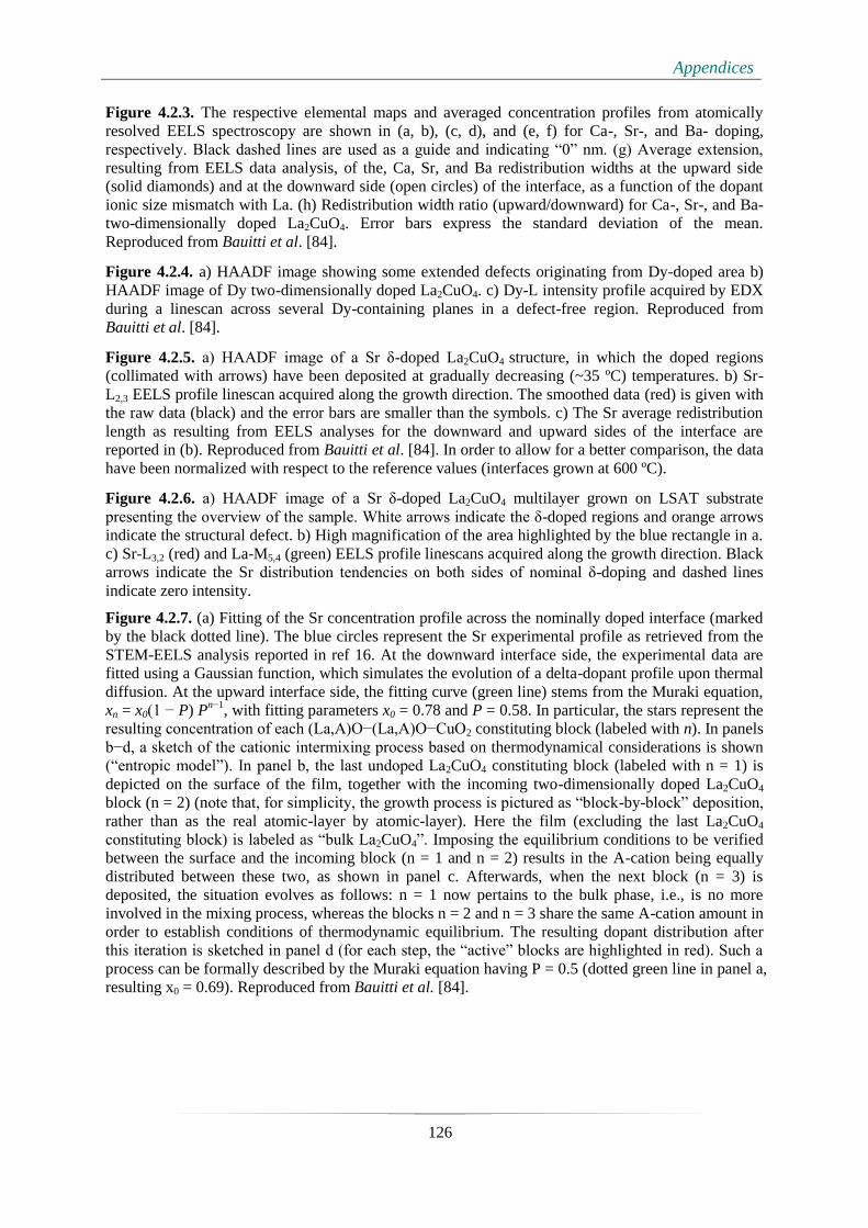
Appendices
126
Figure 4.2.3. The respective elemental maps and averaged concentration profiles from atomically
resolved EELS spectroscopy are shown in (a, b), (c, d), and (e, f) for Ca-, Sr-, and Ba- doping,
respectively. Black dashed lines are used as a guide and indicating “0” nm. (g) Average extension,
resulting from EELS data analysis, of the, Ca, Sr, and Ba redistribution widths at the upward side
(solid diamonds) and at the downward side (open circles) of the interface, as a function of the dopant
ionic size mismatch with La. (h) Redistribution width ratio (upward/downward) for Ca-, Sr-, and Ba-
two-dimensionally doped La2CuO4. Error bars express the standard deviation of the mean.
Reproduced from Bauitti et al. [84].
Figure 4.2.4. a) HAADF image showing some extended defects originating from Dy-doped area b)
HAADF image of Dy two-dimensionally doped La2CuO4. c) Dy-L intensity profile acquired by EDX
during a linescan across several Dy-containing planes in a defect-free region. Reproduced from
Bauitti et al. [84].
Figure 4.2.5. a) HAADF image of a Sr δ-doped La2CuO4 structure, in which the doped regions
(collimated with arrows) have been deposited at gradually decreasing (~35 ºC) temperatures. b) Sr-
L2,3 EELS profile linescan acquired along the growth direction. The smoothed data (red) is given with
the raw data (black) and the error bars are smaller than the symbols. c) The Sr average redistribution
length as resulting from EELS analyses for the downward and upward sides of the interface are
reported in (b). Reproduced from Bauitti et al. [84]. In order to allow for a better comparison, the data
have been normalized with respect to the reference values (interfaces grown at 600 ºC).
Figure 4.2.6. a) HAADF image of a Sr δ-doped La2CuO4 multilayer grown on LSAT substrate
presenting the overview of the sample. White arrows indicate the δ-doped regions and orange arrows
indicate the structural defect. b) High magnification of the area highlighted by the blue rectangle in a.
c) Sr-L3,2 (red) and La-M5,4 (green) EELS profile linescans acquired along the growth direction. Black
arrows indicate the Sr distribution tendencies on both sides of nominal δ-doping and dashed lines
indicate zero intensity.
Figure 4.2.7. (a) Fitting of the Sr concentration profile across the nominally doped interface (marked
by the black dotted line). The blue circles represent the Sr experimental profile as retrieved from the
STEM-EELS analysis reported in ref 16. At the downward interface side, the experimental data are
fitted using a Gaussian function, which simulates the evolution of a delta-dopant profile upon thermal
diffusion. At the upward interface side, the fitting curve (green line) stems from the Muraki equation,
xn = x0(1 − P) Pn−1
, with fitting parameters x0 = 0.78 and P = 0.58. In particular, the stars represent the
resulting concentration of each (La,A)O−(La,A)O−CuO2 constituting block (labeled with n). In panels
b−d, a sketch of the cationic intermixing process based on thermodynamical considerations is shown
(“entropic model”). In panel b, the last undoped La2CuO4 constituting block (labeled with n = 1) is
depicted on the surface of the film, together with the incoming two-dimensionally doped La2CuO4
block (n = 2) (note that, for simplicity, the growth process is pictured as “block-by-block” deposition,
rather than as the real atomic-layer by atomic-layer). Here the film (excluding the last La2CuO4
constituting block) is labeled as “bulk La2CuO4”. Imposing the equilibrium conditions to be verified
between the surface and the incoming block (n = 1 and n = 2) results in the A-cation being equally
distributed between these two, as shown in panel c. Afterwards, when the next block (n = 3) is
deposited, the situation evolves as follows: n = 1 now pertains to the bulk phase, i.e., is no more
involved in the mixing process, whereas the blocks n = 2 and n = 3 share the same A-cation amount in
order to establish conditions of thermodynamic equilibrium. The resulting dopant distribution after
this iteration is sketched in panel d (for each step, the “active” blocks are highlighted in red). Such a
process can be formally described by the Muraki equation having P = 0.5 (dotted green line in panel a,
resulting x0 = 0.69). Reproduced from Bauitti et al. [84].

Appendices
127
Figure 5.1.1: Electrical properties of LCO / LSNO structures. a) Resistance curves as a function
of temperature, for a set of superlattices (N = 2.5) having different doping levels x of LSNO. In order
to allow for a direct comparison between the curves, the resistance values have been normalized to R
(T = 273 K). b) Dependence of Tc on the doping level x for LCO / LSNO superlattices for a set of
representative samples (the corresponding R vs T curves are reported in (a)). c) R vs T for LCO
(bottom layer) / LSNO (top layer) bilayers and d) R vs T for LSNO (bottom layer) / LCO (top layer)
bilayers for representative doping levels x (refer to Figure 5.1.1a for the color legend). Reproduced
from Bauitti et al. [205].
Figure 5.1.2. Dependence of Tc with the LCO thickness for LCO / LSNO superlattices. a) R vs T
curves for 1 x La1.56Sr0.44CuO4 + S x (2.5 x La0.7Sr1.3NiO4 + N x La2CuO4) superlattices, for different
LCO thicknesses N. b) Tc values as a function of the thickness of the LCO phase N for the
La0.7Sr1.3NiO4/La2CuO4 superlattices, whose R vs T curves are reported in (a). Reproduced from
Bauitti et al. [205].
Figure 5.1.3. Low-magnification STEM-HAADF images of (a) x = 0.8 and (b) x = 0.4
LCO/LSNO/LCO trilayers. The images demonstrate the epitaxial quality and the defect-free
structures for both samples. Depending on the different doping (i.e. Sr doping) of the samples the
image contrasts are different.
Figure 5.1.4. STEM imaging and EDX spectroscopy for LCO / LSNO / LCO trilayers. In panels
a) and c), HAADF images of structures in which the doping level of LSNO are x = 0.8 and x = 0.4,
respectively, are displayed. EDX linescans for Ni and Sr are shown in panels b (for x = 0.8) and d (x =
0.4). Reproduced from Bauitti et al. [205].
Figure 5.1.5. HR-STEM investigations at the La2CuO4 / La0.7Sr1.3NiO4 / La2CuO4 interfaces. a)
HAADF image of a the superlattice structure (N = 9). b) Spatial elemental distribution, extracted from
the EELS spectrum image across a La0.7Sr1.3NiO4 region and neighboring LCO areas (the analyzed
region is highlighted by the orange rectangle in panel (a) ). The color code is as follows: La-green,
Cu-red, Ni-orange, Sr-blue. c) EDX signal for Sr (blue) and Ni (orange) (top panel), together with the
simultaneously acquired O-K edge prepeak profile as obtained by an EELS linescan (red line, bottom
panel). The blue and red arrows indicate the upper limits for the Sr and holes distributions,
respectively. Reproduced from Bauitti et al. [205].
Figure 5.1.6. (a) HAADF image showing the line along which the EELS and EDXS line scan was
acquired. (b) Raw EDXS spectrum image. (c) EELS spectrum image of the O-K edge after
background subtraction. (d) Oxygen-K edge from different positions as indicated in Figure (a). The
intensity of the pre-edge peak has been quantified by multi-Gaussian peak fitting using a non-linear
least square (NLLS) routine for all spectra in the line scan profile across several interfaces.
Reproduced from Bauitti et al. [205].
Figure 5.1.7. Sketch of the thermodynamic situation at the boundary layers of LCO and LSNO
(if both are equilibrated with the same oxygen partial pressure and a net transfer of holes and
vacancies occurs from LSNO to LCO). a) The condition of thermodynamic equilibrium for the
defect species (the abbreviations v, i, p, n are used for the building units oxygen vacancies, oxygen
interstitials, electrons and holes respectively) and with the external oxygen partial pressure defines a
horizontal profile for the electrochemical potential of V (�̃�V = 𝜇V + 2𝐹𝜑) and p (𝜇 ̃_𝑝 = 𝜇_𝑝 + 𝐹𝜑),
as well as for the chemical potential of oxygen 𝜇O = −𝜇V + 2𝜇𝑝. Therefore, as a consequence of the
difference in the bulk chemical potentials for the defect species, the bending of 𝜇V and 𝜇𝑝 at the
interface is expected. b) Resulting charge concentration profiles at the interface. Reproduced from
Bauitti et al. [205].
Figure 5.2.1. a) Electrical conductivity and b) Seebeck coefficient of superlattices with different
individual layer thicknesses, as a function of temperature. Reproduced from Kaya et al. [238]

Appendices
128
Figure 5.2.2. a), b) and c) low, intermediate and high-magnification HAADF images of the thick-
layered sample grown on LSAO substrate, respectively. d) XRD pattern of the sample and e) EDXS
line scan profiles of Ni (red) and Cu (blue) along the green arrow in (b) and (c). Reproduced from
Kaya et al. [238].
Figure 5.2.3. a), b) and c) low-, intermediate- and high-magnification HAADF images of the thin-
layered sample grown on LSAO substrate (inset images indicate the corresponding red and green
rectangular regions, blue dashed line indicates the 113-structure). d) XRD pattern of the sample and e)
EDXS line scan profiles of Ni (red) and Cu (blue) along the green arrow in (b) and (c). Reproduced
from Kaya et al. [238]
Figure 5.2.4. Seebeck coefficient (blue) and electrical conductivity (black) of superlattices with thick
constituent layer as a function of temperature obtained experimentally and calculated by applying the
parallel slab model. Reproduced from Kaya et al. [238]
Figure 6.1.1. Basic sketches of the (a) thick-LCO (N = 9) and (b) thin-LCO samples (N = 3). Both of
the samples are composed of 21 repetitions.
Figure 6.1.2. (a) Low magnification STEM-HAADF images of the thick-LCO SL demonstrate the
high-quality epitaxy. (b) STEM-HAADF image intensity profile along the orange arrow in Fig. 1a,
averaged along the perpendicular direction. The image intensity indicates the periodicity of the
contrast related to the Sr distribution at the interfaces. (c) High-magnification image of the area
highlighted by the red rectangle in (a) confirming the structurally coherent 214-113 and 113-214
interfaces.
Figure 6.1.3. (a) Low magnification STEM-HAADF images of the thin-LCO SL demonstrate the
high-quality epitaxy. (b) STEM-HAADF image intensity profile along the orange arrow in Fig. 1a,
averaged along the perpendicular direction. The image intensity indicates the periodicity of the
contrast related to the Sr distribution at the interfaces. (c) High-magnification image of the area
highlighted by the red rectangle in (a) confirming the structurally coherent 214-113 and 113-214
interfaces.
Figure 6.1.4. The atomically resolved elemental maps obtained via EELS spectroscopy, are displayed
in panels a), b), c) and d) for Sr (blue), La (green), Mn (red), and Cu (cyan) respectively. e) displays
the overlay of the three elements. f) shows the Sr distribution profiles across both interfaces. The
linear distortion in the experimental spectrum image is corrected via STEM SI Warp software [129]
for the Sr profile plot in (f). Please note that, for clarity, the nominal SrMnO3 and Sr δ-doped
La2CuO4 layers are shaded light-blue.
Figure 6.1.5. a) STEM-ABF image displaying all atomic column positions including O-column
positions. b) O–O interatomic distances along basal (in-plane) and apical (out-of-plane) directions
exhibit the variations across the interfaces. c) The STEM-HAADF image displays the coherent
interfaces and the weaker contrast in the Sr-rich region (1-2 MLs). d) La–La interatomic distances
along basal (in-plane) and apical (out-of-plane) directions exhibit the variations across the interfaces.
The blue and orange arrows on the images indicate the nominal 214-113 and 113-214 interfaces. The
apical and basal distances are indicated with straight and dashed lines, respectively. The error bars
give the 95% confidence interval (corresponding to 2 times the standard error) of the average of 14
unit cells of the perovskite lattice along the basal (in-plane) direction.

Appendices
129
Figure 7.1.1. (a) Depiction of the NdNiO3 unit cell (black lines) in orthorhombic space group Pbnm.
The planes corresponding to the [011] –and [101]– cut (α- and β-cut) are indicated in blue and red,
respectively. For clarity only one NiO6 octahedron (gray) is superimposed to the unit cell. (b)
Schematic of the interconnectivity of the octahedral network across the epitaxial NdNiO3–NdGaO3
interface. One NiO6 octahedron (gray) is shown in proximity to the α-cut NdGaO3 substrate surface
(blue). Each interfacial NdNiO3 octahedron connects to three NdGaO3 octahedra (black arrows). (c)-
(f) Illustration of the in-plane epitaxial strain induced to the NdNiO3 unit cell (gray rectangular) by an
underlying NdGaO3 substrate (orange rectangular) for different combinations of α -and β-cuts. The
indicated in-plane directions of the projected unit cells lie within the α- and β-planes. Unit cell
dimensions are exaggerated for clarity. The numbers are the strain magnitudes along these directions
calculated as explained in the text. Note that the effective strains for the growth modes α on α (c) and
β on α (f) are closely similar.
Figure 7.1.2. a) STEM-HAADF image of the NdNiO3 thin film with a thickness of 11.4 nm on a
[011] oriented NdGaO3 substrate. The image illustrates the high epitaxial quality and the defect-free
structure of the film. The inset is a high-resolution STEM-HAADF image of the film-substrate
interface region. b) EDS line scan profiles along the [011] growth direction indicated by the yellow
arrow presenting the chemical composition of the NdGaO3-NdNiO3 interface. The orange, black, and
gray lines correspond to the EDS intensity of the Ga K, Nd L, Ni K, and lines, respectively.
Intermixing of Ni and Ga atomic species in the interface region of ~1.5 nm is marked by the shaded
area. The interface is defined at 0 nm and the dashed line corresponds to zero intensity of the EDS. c)
STEM-LAADF image with NdNiO3 epitaxial layer indicated by the orange arrow. No structural
defects and/or structural grains can be detected, substantiating high crystalline quality. The layer on
top of NdNiO3 is the glue from the specimen preparation. The blue box represents the dimensions of
the STEM-HAADF image in (a).
Figure 7.1.3. a) STEM-HAADF image taken along the epitaxial layer including the
substrate/epitaxial layer interface. Blue and green arrows indicate measured out-of-plane and in-plane
Nd–Nd interatomic distances, respectively, shown in (b) and (c). d) STEM-ABF image,
simultaneously acquired with the STEM-HAADF image in (a), providing the oxygen column
positions, and (e) Ni‒O‒Ni bond angle measurements performed on the ABF image shown in (d). The
orange lines and the dashed lines mark the nominal interface in the images and the plots, respectively.
The error bars of the bond angle determination (95% confidence interval, corresponding to 2 times the
standard error) is less than 1º. The blue and red colored areas are guides for the eye indicating the α-
and β-phases, respectively.
Figure 7.1.4. DFT+U ground state for different epitaxial configurations depicted in Figure 7.1.1(e-f).
a) In-plane lattice constants of NdNiO3 are fixed at the values corresponding to the α-cut NdGaO3,
while the NdNiO3 out-of-plane lattice constant is allowed to relax, simulating the effects of epitaxy on
an α-NdGaO3 substrate surface. The NdNiO3 in-plane directions are [100] and [01-1], and the out-
plane is [011] for the α-phase calculation (blue curve). For the β-phase calculation, in-plane directions
are [010] and [-101] and the out-plane direction is [101] (red curve). The global minimum is obtained
for the β-phase calculation indicating the energetically most favorable state that corresponds to β-
phase NdNiO3 unit cells in epitaxy to the α-phase NdGaO3 substrate. This explains the experimentally
observed reorientation of NdNiO3 grown on α-cut NdGaO3. Furthermore, the magnitude of the
octahedral breathing distortion in the NdNiO3 β-phase ground state is strongly enhanced which
promotes its emergence. b) Analogous calculation to (a), but with NdNiO3 in-plane lattice fixed at
values corresponding to β-cut NdGaO3. The global minimum is obtained within the beta-phase
calculation suggesting that no reorientation takes place in case NdNiO3 is grown on β-cut NdGaO3.
Appendices
130
Symbols and abbreviations
List of most used abbreviations
ABF Annular bright field
AFM Atomic force microscopy
ALL Atomic-layer-by-layer
EDXS Energy dispersive X-ray spectroscopy
EELS Electron energy loss spectroscopy
HAADF High-angle annular dark field
HT-IS High-temperature interface superconductivity
HTSC High-temperature superconductivity
LBCO La2-xBaxCuO4
LCO La2CuO4
LCCO La2-xCaxCuO4
LSCO La2-xSrxCuO4
LNO La2NiO4; LaNiO3
LSAO LaSrAlO4
MBE Molecular beam epitaxy
MSA Multivariate statistical analysis
NNO NdNiO3
NGO NdGaO3
PCA Principal component analyses
STEM Scanning transmission electron microscopy
STO SrTiO3
TEM Transmission electron microscopy
TMO Transition metal oxide
RHEED Reflection high-energy electron diffraction
XRD X-ray diffraction

Appendices
131
List of most used symbols
ℎ• Electron hole according to the Kröger-Vink notation
δ Oxygen nonstoichiometry
ρ Electrical resistivity
n Electron concentration
P Pressure
p Electron hole concentration
T Temperature
Tc Superconducting critical temperature
𝑉𝑂•• Oxygen vacancy according to the Kröger-Vink notation
𝑂𝑖′′ Oxygen interstitial according to the Kröger-Vink notation

Appendices
132
Declaration
Hereby I declare that this thesis titled, “Atomic-Scale Control and Characterization of Oxide
Heterostructures: Correlating Interfacial Structure and Novel Functionalities” has been independently
carried out by me at the Stuttgart Center for Electron Microscopy (StEM), Max Planck Institute for
Solid State Research in partial fulfillment of the requirements for the degree of Doctor of Natural
Science (Dr. rer. nat.) in Materials Science from the Technical University of Darmstadt (TU
Darmstadt). I certify that the work presented in this thesis is, to the best of my knowledge and belief,
original and contains no material previously published or written by another person, except where due
reference and permission is made.
Stuttgart
13.11.2018 Y. Eren Suyolcu

Bibliography
133
Bibliography [1] D.G. Schlom, J. Mannhart, Oxide electronics: Interface takes charge over Si, Nat. Mater. 10
(2011) 168–169. doi:10.1038/nmat2965.
[2] J. Mannhart, D.G. Schlom, Oxide Interface - An Opportunity for Electronics, Science. 327
(2010) 1607–1611. doi:10.1126/science.1181862.
[3] P. Zubko, S. Gariglio, M. Gabay, P. Ghosez, J.-M. Triscone, Interface Physics in Complex
Oxide Heterostructures, Annu. Rev. Condens. Matter Phys. 2 (2011) 141–165. doi:10.1146/annurev-
conmatphys-062910-140445.
[4] H.Y. Hwang, Y. Iwasa, M. Kawasaki, B. Keimer, N. Nagaosa, Y. Tokura, Emergent phenomena
at oxide interfaces, Nat. Mater. 11 (2012) 103–113. doi:10.1038/nmat3223.
[5] J.B. Torrance, P. Lacorre, A.I. Nazzal, E.J. Ansaldo, Ch. Niedermayer, Systematic study of
insulator-metal transitions in perovskites RNiO3 (R=Pr,Nd,Sm,Eu) due to closing of charge-transfer
gap, Phys. Rev. B. 45 (1992) 8209–8212. doi:10.1103/PhysRevB.45.8209.
[6] J. Chakhalian, J.W. Freeland, H.-U. Habermeier, G. Cristiani, G. Khaliullin, M. van
Veenendaal, B. Keimer, Orbital Reconstruction and Covalent Bonding at an Oxide Interface, Science.
318 (2007) 1114–1117. doi:10.1126/science.1149338.
[7] S. Jin, M. McCormack, T.H. Tiefel, R. Ramesh, Colossal magnetoresistance in La-Ca-Mn-O
ferromagnetic thin films (invited), J. Appl. Phys. 76 (1994) 6929–6933. doi:10.1063/1.358119.
[8] Y. Tokura, Y. Tomioka, Colossal magnetoresistive manganites, J. Magn. Magn. Mater. 200
(1999) 1–23. doi:10.1016/S0304-8853(99)00352-2.
[9] N. Reyren, S. Thiel, A.D. Caviglia, L.F. Kourkoutis, G. Hammerl, C. Richter, C.W. Schneider,
T. Kopp, A.-S. Rüetschi, D. Jaccard, M. Gabay, D.A. Muller, J.-M. Triscone, J. Mannhart,
Superconducting Interfaces Between Insulating Oxides, Science. 317 (2007) 1196–1199.
doi:10.1126/science.1146006.
[10] A. Gozar, G. Logvenov, L.F. Kourkoutis, A.T. Bollinger, L.A. Giannuzzi, D.A. Muller, I.
Bozovic, High-temperature interface superconductivity between metallic and insulating copper oxides,
Nature. 455 (2008) 782–785. doi:10.1038/nature07293.
[11] C. He, A.J. Grutter, M. Gu, N.D. Browning, Y. Takamura, B.J. Kirby, J.A. Borchers, J.W. Kim,
M.R. Fitzsimmons, X. Zhai, V.V. Mehta, F.J. Wong, Y. Suzuki, Interfacial Ferromagnetism and
Exchange Bias in CaRuO3/CaMnO3 Superlattices, Phys. Rev. Lett. 109 (2012) 197202.
doi:10.1103/PhysRevLett.109.197202.
[12] A. Ohtomo, H.Y. Hwang, A high-mobility electron gas at the LaAlO3/SrTiO3 heterointerface,
Nature. 427 (2004) 423–426. doi:10.1038/nature02308.
[13] H. Ohta, S. Kim, Y. Mune, T. Mizoguchi, K. Nomura, S. Ohta, T. Nomura, Y. Nakanishi, Y.
Ikuhara, M. Hirano, H. Hosono, K. Koumoto, Giant thermoelectric Seebeck coefficient of a two-
dimensional electron gas in SrTiO3, Nat. Mater. 6 (2007) 129–134. doi:10.1038/nmat1821.
[14] S.A. Chambers, Epitaxial Growth and Properties of Doped Transition Metal and Complex
Oxide Films, Adv. Mater. 22 (2010) 219–248. doi:10.1002/adma.200901867.
[15] D.G. Schlom, L.-Q. Chen, X. Pan, A. Schmehl, M.A. Zurbuchen, A Thin Film Approach to
Engineering Functionality into Oxides, J. Am. Ceram. Soc. 91 (2008) 2429–2454. doi:10.1111/j.1551-
2916.2008.02556.x.
[16] Y.E. Suyolcu, Y. Wang, W. Sigle, G. Cristiani, G. Logvenov, P.A. van Aken, Linking Dopant
Distribution and Interatomic Distortions at La1.6M0.4CuO4/La2CuO4 Superconducting Interfaces,
Microsc. Microanal. 22 (2016) 308–309. doi:10.1017/S1431927616002397.

Bibliography
134
[17] J. Maier, Nanoionics: ion transport and electrochemical storage in confined systems, Nat. Mater.
4 (2005) 805–815. doi:10.1038/nmat1513.
[18] R. Ramesh, N.A. Spaldin, Multiferroics: progress and prospects in thin films, Nat. Mater. 6
(2007) nmat1805. doi:10.1038/nmat1805.
[19] V.M. Goldschmidt, Die Gesetze der Krystallochemie, Naturwissenschaften. 14 (1926) 477–485.
doi:10.1007/BF01507527.
[20] D. Lee, H.N. Lee, Controlling Oxygen Mobility in Ruddlesden–Popper Oxides, Materials. 10
(2017) 368. doi:10.3390/ma10040368.
[21] J.H. Van Vleck, Theory of the Variations in Paramagnetic Anisotropy Among Different Salts of
the Iron Group, Phys. Rev. 41 (1932) 208–215. doi:10.1103/PhysRev.41.208.
[22] Y. Tokura, N. Nagaosa, Orbital Physics in Transition-Metal Oxides, Science. 288 (2000) 462–
468. doi:10.1126/science.288.5465.462.
[23] H.A. Jahn, E. Teller, Stability of Polyatomic Molecules in Degenerate Electronic States. I.
Orbital Degeneracy, Proc. R. Soc. Lond. Math. Phys. Eng. Sci. 161 (1937) 220–235.
doi:10.1098/rspa.1937.0142.
[24] J. Kanamori, Crystal Distortion in Magnetic Compounds, J. Appl. Phys. 31 (1960) S14–S23.
doi:10.1063/1.1984590.
[25] M. A. Halcrow, Jahn–Teller distortions in transition metal compounds, and their importance in
functional molecular and inorganic materials, Chem. Soc. Rev. 42 (2013) 1784–1795.
doi:10.1039/C2CS35253B.
[26] Kamimura, H., Theory of Copper Oxide superconductors, Springer, New York, 2005.
[27] J.B. Boyce, F. Bridges, T. Claeson, T.H. Geballe, C.W. Chu, J.M. Tarascon, X-ray-absorption
studies of the high-Tc superconductors La1.8Sr0.2CuO4 and La1.8Ba0.2CuO4, Phys. Rev. B. 35 (1987)
7203–7206. doi:10.1103/PhysRevB.35.7203.
[28] M.W. Lufaso, P.M. Woodward, Jahn–Teller distortions, cation ordering and octahedral tilting in
perovskites, Acta Crystallogr. B. 60 (2004) 10–20. doi:10.1107/S0108768103026661.
[29] D. Haskel, V. Polinger, E.A. Stern, Where do the doped holes go in La2−xSrxCuO4? A close look
by XAFS, in: AIP Conf. Proc., AIP Publishing, 1999: pp. 241–246. doi:10.1063/1.59594.
[30] V. Polinger, D. Haskel, E.A. Stern, Dopant Induced Enhancement of the Jahn–Teller Effect in
Perovskite Cuprates, in: M.D. Kaplan, G.O. Zimmerman (Eds.), Vibronic Interact. Jahn–Teller Eff.
Cryst. Mol., Springer Netherlands, 2001: pp. 215–219. doi:10.1007/978-94-010-0985-0_23.
[31] K. Shiraishi, Dr. of Science Thesis, University of Tokyo, 1988.
[32] P.G. Radaelli, D.G. Hinks, A.W. Mitchell, B.A. Hunter, J.L. Wagner, B. Dabrowski, K.G.
Vandervoort, H.K. Viswanathan, J.D. Jorgensen, Structural and superconducting properties of La2-
xSrxCuO4 as a function of Sr content, Phys. Rev. B. 49 (1994) 4163–4175.
doi:10.1103/PhysRevB.49.4163.
[33] Y. Wang, F. Baiutti, G. Gregori, G. Cristiani, U. Salzberger, G. Logvenov, J. Maier, P.A. van
Aken, Atomic-Scale Quantitative Analysis of Lattice Distortions at Interfaces of Two-Dimensionally
Sr-Doped La2CuO4 Superlattices, ACS Appl. Mater. Interfaces. 8 (2016) 6763–6769.
doi:10.1021/acsami.5b12813.
[34] H. Zhou, Y. Yacoby, V.Y. Butko, G. Logvenov, I. Božović, R. Pindak, Anomalous expansion
of the copper-apical-oxygen distance in superconducting cuprate bilayers, Proc. Natl. Acad. Sci. 107
(2010) 8103–8107. doi:10.1073/pnas.0914702107.
[35] H. Kamimura, T. Hamada, S. Matsuno, H. Ushio, A Novel Approach to the Polaronic Metallic
State of Cuprate Superconductors and the d-Wave Pairing Mechanism, J. Supercond. 15 (2002) 379–
385. doi:10.1023/A:1021078415473.

Bibliography
135
[36] S.-W. Cheong, J.D. Thompson, Z. Fisk, Properties of La2CuO4 and related compounds, Phys. C
Supercond. 158 (1989) 109–126. doi:10.1016/0921-4534(89)90306-7.
[37] P. Babkevich, D. Prabhakaran, C.D. Frost, A.T. Boothroyd, Magnetic spectrum of the two-
dimensional antiferromagnet La2CoO4 studied by inelastic neutron scattering, Phys. Rev. B. 82 (2010)
184425. doi:10.1103/PhysRevB.82.184425.
[38] K. Yamada, M. Matsuda, Y. Endoh, B. Keimer, R.J. Birgeneau, S. Onodera, J. Mizusaki, T.
Matsuura, G. Shirane, Successive antiferromagnetic phase transitions in single-crystal La2CoO4, Phys.
Rev. B. 39 (1989) 2336–2343. doi:10.1103/PhysRevB.39.2336.
[39] W. Paulus, A. Cousson, G. Dhalenne, J. Berthon, A. Revcolevschi, S. Hosoya, W. Treutmann,
G. Heger, R. Le Toquin, Neutron diffraction studies of stoichiometric and oxygen intercalated
La2NiO4 single crystals, Solid State Sci. 4 (2002) 565–573. doi:10.1016/S1293-2558(02)01299-2.
[40] J.G. Bednorz, K.A. Müller, Possible high Tc superconductivity in the Ba−La−Cu−O system, Z.
Für Phys. B Condens. Matter. 64 (1986) 189–193. doi:10.1007/BF01303701.
[41] A. Schilling, M. Cantoni, J.D. Guo, H.R. Ott, Superconductivity above 130 K in the Hg–Ba–
Ca–Cu–O system, Nature. 363 (1993) 56–58. doi:10.1038/363056a0.
[42] C.W. Chu, L. Gao, F. Chen, Z.J. Huang, R.L. Meng, Y.Y. Xue, Superconductivity above 150 K
in HgBa2Ca2Cu3O8+δ at high pressures, Nature. 365 (1993) 323–325. doi:10.1038/365323a0.
[43] L. Gao, Y.Y. Xue, F. Chen, Q. Xiong, R.L. Meng, D. Ramirez, C.W. Chu, J.H. Eggert, H.K.
Mao, Superconductivity up to 164 K in HgBa2Cam-1CumO2m+2+δ (m=1, 2, and 3) under quasihydrostatic
pressures, Phys. Rev. B. 50 (1994) 4260–4263. doi:10.1103/PhysRevB.50.4260.
[44] B. Keimer, S.A. Kivelson, M.R. Norman, S. Uchida, J. Zaanen, From quantum matter to high-
temperature superconductivity in copper oxides, Nature. 518 (2015) 179–186.
doi:10.1038/nature14165.
[45] H. Sato, A. Tsukada, M. Naito, A. Matsuda, La2-xSrxCuOy epitaxial thin films (x=0 to 2):
Structure, strain, and superconductivity, Phys. Rev. B. 61 (2000) 12447–12456.
doi:10.1103/PhysRevB.61.12447.
[46] Y. Ando, S. Komiya, K. Segawa, S. Ono, Y. Kurita, Electronic Phase Diagram of High-Tc
Cuprate Superconductors from a Mapping of the In-Plane Resistivity Curvature, Phys. Rev. Lett. 93
(2004) 267001. doi:10.1103/PhysRevLett.93.267001.
[47] L. Taillefer, Scattering and Pairing in Cuprate Superconductors, Annu. Rev. Condens. Matter
Phys. 1 (2010) 51–70. doi:10.1146/annurev-conmatphys-070909-104117.
[48] J. Bardeen, L.N. Cooper, J.R. Schrieffer, Theory of Superconductivity, Phys. Rev. 108 (1957)
1175–1204. doi:10.1103/PhysRev.108.1175.
[49] M. Hashimoto, I.M. Vishik, R.-H. He, T.P. Devereaux, Z.-X. Shen, Energy gaps in high-
transition-temperature cuprate superconductors, Nat. Phys. 10 (2014) 483–495.
doi:10.1038/nphys3009.
[50] H. Keller, A. Bussmann-Holder, K.A. Müller, Jahn–Teller physics and high-Tc
superconductivity, Mater. Today. 11 (2008) 38–46. doi:10.1016/S1369-7021(08)70178-0.
[51] G. Logvenov, A. Gozar, I. Bozovic, High-Temperature Superconductivity in a Single Copper-
Oxygen Plane, Science. 326 (2009) 699–702. doi:10.1126/science.1178863.
[52] V.Y. Butko, G. Logvenov, N. Božović, Z. Radović, I. Božović, Madelung Strain in Cuprate
Superconductors – A Route to Enhancement of the Critical Temperature, Adv. Mater. 21 (2009)
3644–3648. doi:10.1002/adma.200803850.
[53] H. Sato, M. Naito, Increase in the superconducting transition temperature by anisotropic strain
effect in (001) La1.85Sr0.15CuO4 thin films on LaSrAlO4 substrates, Phys. C Supercond. 274 (1997)
221–226. doi:10.1016/S0921-4534(96)00675-2.

Bibliography
136
[54] J.-P. Locquet, J. Perret, J. Fompeyrine, E. Mächler, J.W. Seo, G. Van Tendeloo, Doubling the
critical temperature of La1.9Sr0.1CuO4 using epitaxial strain, Nature. 394 (1998) 453–456.
doi:10.1038/28810.
[55] F. Baiutti, G. Logvenov, G. Gregori, G. Cristiani, Y. Wang, W. Sigle, P.A. van Aken, J. Maier,
High-temperature superconductivity in space-charge regions of lanthanum cuprate induced by two-
dimensional doping, Nat. Commun. 6 (2015) 8586. doi:10.1038/ncomms9586.
[56] S. Shinomori, Y. Okimoto, M. Kawasaki, Y. Tokura, Insulator-Metal Transition in La2-
xSrxNiO4, J. Phys. Soc. Jpn. 71 (2002) 705–708. doi:10.1143/JPSJ.71.705.
[57] P. Briois, F. Perry, A. Billard, Structural and electrical characterisation of lanthanum nickelate
reactively sputter-deposited thin films, Thin Solid Films. 516 (2008) 3282–3286.
doi:10.1016/j.tsf.2007.08.107.
[58] J. Zhang, A.S. Botana, J.W. Freeland, D. Phelan, H. Zheng, V. Pardo, M.R. Norman, J.F.
Mitchell, Large orbital polarization in a metallic square-planar nickelate, Nat. Phys. 13 (2017) 864–
869. doi:10.1038/nphys4149.
[59] M.L. Medarde, Structural, magnetic and electronic properties of RNiO3 perovskites (R = rare
earth), J. Phys. Condens. Matter. 9 (1997) 1679. doi:10.1088/0953-8984/9/8/003.
[60] F. Wrobel, Structural and electronic properties of nickelate heterostructures, (2016).
doi:http://dx.doi.org/10.18419/opus-8924.
[61] F. Baiutti, Heterogeneous doping and superconductivity in La2CuO4-based heterostructures,
University of Stuttgart, 2015. http://elib.uni-stuttgart.de/handle/11682/6901 (accessed October 28,
2016).
[62] A. Bhattacharya, S.J. May, Magnetic Oxide Heterostructures, Annu. Rev. Mater. Res. 44 (2014)
65–90. doi:10.1146/annurev-matsci-070813-113447.
[63] P. Ravindran, A. Kjekshus, H. Fjellvåg, A. Delin, O. Eriksson, Ground-state and excited-state
properties of LaMnO3 from full-potential calculations, Phys. Rev. B. 65 (2002) 064445.
doi:10.1103/PhysRevB.65.064445.
[64] I. Loa, P. Adler, A. Grzechnik, K. Syassen, U. Schwarz, M. Hanfland, G.Kh. Rozenberg, P.
Gorodetsky, M.P. Pasternak, Pressure-Induced Quenching of the Jahn–Teller Distortion and Insulator-
to-Metal Transition in LaMnO3, Phys. Rev. Lett. 87 (2001) 125501.
doi:10.1103/PhysRevLett.87.125501.
[65] H. Chen, A.J. Millis, Phase diagram of Sr1-xBaxMnO3 as a function of chemical doping, epitaxial
strain, and external pressure, Phys. Rev. B. 94 (2016) 165106. doi:10.1103/PhysRevB.94.165106.
[66] J.J. Adkin, M.A. Hayward, BaMnO3-x Revisited: A Structural and Magnetic Study, Chem.
Mater. 19 (2007) 755–762. doi:10.1021/cm062055r.
[67] Y. Syono, S. Akimoto, K. Kohn, Structure Relations of Hexagonal Perovskite-Like Compounds
ABX3 at High Pressure, J. Phys. Soc. Jpn. 26 (1969) 993–999. doi:10.1143/JPSJ.26.993.
[68] R. Søndenå, P. Ravindran, S. Stølen, T. Grande, M. Hanfland, Electronic structure and magnetic
properties of cubic and hexagonal SrMnO3, Phys. Rev. B. 74 (2006) 144102.
doi:10.1103/PhysRevB.74.144102.
[69] K.R. Poeppelmeier, M.E. Leonowicz, J.C. Scanlon, J.M. Longo, W.B. Yelon, Structure
determination of CaMnO3 and CaMnO2.5 by X-ray and neutron methods, J. Solid State Chem. 45
(1982) 71–79. doi:10.1016/0022-4596(82)90292-4.
[70] P.W. Anderson, Antiferromagnetism. Theory of Superexchange Interaction, Phys. Rev. 79
(1950) 350–356. doi:10.1103/PhysRev.79.350.
[71] J.B. Goodenough, Theory of the Role of Covalence in the Perovskite-Type Manganites [La,
M(II)]MnO3, Phys. Rev. 100 (1955) 564–573. doi:10.1103/PhysRev.100.564.

Bibliography
137
[72] C. Zener, Interaction between the d-Shells in the Transition Metals. II. Ferromagnetic
Compounds of Manganese with Perovskite Structure, Phys. Rev. 82 (1951) 403–405.
doi:10.1103/PhysRev.82.403.
[73] N. Nguyen, J. Choisnet, M. Hervieu, B. Raveau, Oxygen defect K2NiF4-type oxides: The
compounds La2−xSrxCuO4−x/2+δ, J. Solid State Chem. 39 (1981) 120–127. doi:10.1016/0022-
4596(81)90310-8.
[74] J. Maier, G. Pfundtner, Defect chemistry of the high-Tc superconductors, Adv. Mater. 3 (1991)
292–297. doi:10.1002/adma.19910030605.
[75] L. Shen, P. Salvador, T.O. Mason, K. Fueki, High temperature electrical properties and defect
chemistry of La2-xCaxCuO4-y superconductors—II. Defect structure modeling, J. Phys. Chem. Solids.
57 (1996) 1977–1987. doi:10.1016/S0022-3697(95)00324-X.
[76] A.R. Moodenbaugh, Y. Xu, M. Suenaga, T.J. Folkerts, R.N. Shelton, Superconducting
properties of La2-xBaxCuO, Phys. Rev. B. 38 (1988) 4596–4600. doi:10.1103/PhysRevB.38.4596.
[77] A.R. Moodenbaugh, R.L. Sabatini, Y. Xu, J. Ochab, J.G. Huber, Solubility of Ca in
superconducting La2−xCaxCuO4, Phys. C Supercond. 198 (1992) 103–108. doi:10.1016/0921-
4534(92)90272-E.
[78] J. Maier, Physical Chemistry of Ionic Materials: Ions and Electrons in Solids, John Wiley &
Sons, Ltd, Chichester, UK, 2004. doi:10.1002/0470020229.
[79] Y.E. Suyolcu, Y. Wang, F. Baiutti, A. Al-Temimy, G. Gregori, G. Cristiani, W. Sigle, J. Maier,
P.A. van Aken, G. Logvenov, Dopant size effects on novel functionalities: High-temperature
interfacial superconductivity, Sci. Rep. 7 (2017) 453. doi:10.1038/s41598-017-00539-4.
[80] J.B. Torrance, Y. Tokura, A.I. Nazzal, A. Bezinge, T.C. Huang, S.S.P. Parkin, Anomalous
Disappearance of High-Tc Superconductivity at High Hole Concentration in Metallic La2-xSrxCuO4,
Phys. Rev. Lett. 61 (1988) 1127–1130. doi:10.1103/PhysRevLett.61.1127.
[81] D.E. Rice, D.J. Buttrey, An X-Ray Diffraction Study of the Oxygen Content Phase Diagram of
La2NiO4+δ, J. Solid State Chem. 105 (1993) 197–210. doi:10.1006/jssc.1993.1208.
[82] J.P. Tang, R.I. Dass, A. Manthiram, Comparison of the crystal chemistry and electrical
properties of La2−xAxNiO4 (A = Ca, Sr, and Ba), Mater. Res. Bull. 35 (2000) 411–424.
doi:10.1016/S0025-5408(00)00234-8.
[83] J. Maier, Space charge regions in solid two-phase systems and their conduction contribution-I.
Conductance enhancement in the system ionic conductor-’inert’ phase and application on AgC1:Al2O3
and AgC1:SiO2, J. Phys. Chem. Solids. 46 (1985) 309–320. doi:10.1016/0022-3697(85)90172-6.
[84] F. Baiutti, G. Gregori, Y. Wang, Y.E. Suyolcu, G. Cristiani, P.A. van Aken, J. Maier, G.
Logvenov, Cationic Redistribution at Epitaxial Interfaces in Superconducting Two-Dimensionally
Doped Lanthanum Cuprate Films, ACS Appl. Mater. Interfaces. 8 (2016) 27368–27375.
doi:10.1021/acsami.6b09739.
[85] F. Wrobel, A.F. Mark, G. Christiani, W. Sigle, H.-U. Habermeier, P.A. van Aken, G. Logvenov,
B. Keimer, E. Benckiser, Comparative study of LaNiO3/LaAlO3 heterostructures grown by pulsed
laser deposition and oxide molecular beam epitaxy, Appl. Phys. Lett. 110 (2017) 041606.
doi:10.1063/1.4975005.
[86] D.G. Schlom, L.-Q. Chen, C.-B. Eom, K.M. Rabe, S.K. Streiffer, J.-M. Triscone, Strain Tuning
of Ferroelectric Thin Films, Annu. Rev. Mater. Res. 37 (2007) 589–626.
doi:10.1146/annurev.matsci.37.061206.113016.
[87] I. Bozovic, G. Logvenov, I. Belca, B. Narimbetov, I. Sveklo, Epitaxial Strain and
Superconductivity in La2-xSrxCuO4 Thin Films, Phys. Rev. Lett. 89 (2002) 107001.
doi:10.1103/PhysRevLett.89.107001.
[88] C.L. Jia, X.H. Zeng, X.X. Xi, K. Urban, Microstructure and residual strain in La2CuO4 thin

Bibliography
138
films on LaSrAlO4-buffered SrTiO3 substrates, Phys. Rev. B. 64 (2001) 075416.
doi:10.1103/PhysRevB.64.075416.
[89] Y.E. Suyolcu, Y. Wang, W. Sigle, F. Baiutti, G. Cristiani, G. Logvenov, J. Maier, P.A. van
Aken, Octahedral Distortions at High-Temperature Superconducting La2CuO4 Interfaces: Visualizing
Jahn–Teller Effects, Adv. Mater. Interfaces. 4 (2017) 1700737. doi:10.1002/admi.201700737.
[90] D.G. Schlom, J.N. Eckstein, E.S. Hellman, S.K. Streiffer, J.S. Harris, M.R. Beasley, J.C.
Bravman, T.H. Geballe, C. Webb, K.E. von Dessonneck, F. Turner, Molecular beam epitaxy of
layered Dy‐ Ba‐ Cu‐ O compounds, Appl. Phys. Lett. 53 (1988) 1660–1662. doi:10.1063/1.100443.
[91] M.G. Lagally, D.E. Savage, Quantitative Electron Diffraction from Thin Films, MRS Bull. 18
(1993) 24–31. doi:10.1557/S0883769400043414.
[92] G.J.H.M. Rijnders, G. Koster, D.H.A. Blank, H. Rogalla, In situ monitoring during pulsed laser
deposition of complex oxides using reflection high energy electron diffraction under high oxygen
pressure, Appl. Phys. Lett. 70 (1997) 1888–1890. doi:10.1063/1.118687.
[93] T. Terashima, Y. Bando, K. Iijima, K. Yamamoto, K. Hirata, K. Hayashi, K. Kamigaki, H.
Terauchi, Reflection high-energy electron diffraction oscillations during epitaxial growth of high-
temperature superconducting oxides, Phys. Rev. Lett. 65 (1990) 2684–2687.
doi:10.1103/PhysRevLett.65.2684.
[94] I. Bozovic, J.N. Eckstein, Analysis of Growing Films of Complex Oxides by RHEED, MRS
Bull. 20 (1995) 32–38. doi:10.1557/S0883769400044870.
[95] W. Braun, Monitoring surface roughness during film growth using modulated RHEED intensity
oscillations, J. Cryst. Growth. 477 (2017) 34–39. doi:10.1016/j.jcrysgro.2016.12.082.
[96] R.D. Shannon, Revised effective ionic radii and systematic studies of interatomic distances in
halides and chalcogenides, Acta Crystallogr. Sect. A. 32 (1976) 751–767.
doi:10.1107/S0567739476001551.
[97] G. Kim, G. Christiani, G. Logvenov, S. Choi, H.-H. Kim, M. Minola, B. Keimer, Selective
formation of apical oxygen vacancies in La2-xSrxCuO4, Phys. Rev. Mater. 1 (2017) 054801.
doi:10.1103/PhysRevMaterials.1.054801.
[98] Y.E. Suyolcu, G. Cristiani, P.A. van Aken, G. Logvenov, Understanding of the surface
reconstruction during epitaxial growth of (LaSr)2CuO4 thin films, (unpublished results).
[99] W. Lee, J.W. Han, Y. Chen, Z. Cai, B. Yildiz, Cation Size Mismatch and Charge Interactions
Drive Dopant Segregation at the Surfaces of Manganite Perovskites, J. Am. Chem. Soc. 135 (2013)
7909–7925. doi:10.1021/ja3125349.
[100] C.B. Carter, D.B. Williams, eds., Transmission Electron Microscopy, Springer International
Publishing, Cham, 2016. doi:10.1007/978-3-319-26651-0.
[101] S.J. Pennycook, P.D. Nellist, eds., Scanning Transmission Electron Microscopy, Springer New
York, New York, NY, 2011. doi:10.1007/978-1-4419-7200-2.
[102] Allied High Tech - MultiPrepTM
Polishing System - 8", (n.d.).
http://www.alliedhightech.com/Equipment/multiprep-polishing-system-8 (accessed February 9, 2017).
[103] T. Malis, S.C. Cheng, R.F. Egerton, EELS log-ratio technique for specimen-thickness
measurement in the TEM, J. Electron Microsc. Tech. 8 (1988) 193–200.
doi:10.1002/jemt.1060080206.
[104] M. Haider, S. Uhlemann, E. Schwan, H. Rose, B. Kabius, K. Urban, Electron microscopy image
enhanced, Nature. 392 (1998) 768–769. doi:10.1038/33823.
[105] S.J. Pennycook, D.E. Jesson, High-resolution incoherent imaging of crystals, Phys. Rev. Lett.
64 (1990) 938–941. doi:10.1103/PhysRevLett.64.938.
[106] S.D. Findlay, N. Shibata, H. Sawada, E. Okunishi, Y. Kondo, T. Yamamoto, Y. Ikuhara, Robust

Bibliography
139
atomic resolution imaging of light elements using scanning transmission electron microscopy, Appl.
Phys. Lett. 95 (2009) 191913. doi:10.1063/1.3265946.
[107] E. Okunishi, I. Ishikawa, H. Sawada, F. Hosokawa, M. Hori, Y. Kondo, Visualization of Light
Elements at Ultrahigh Resolution by STEM Annular Bright Field Microscopy, Microsc. Microanal. 15
(2009) 164–165. doi:10.1017/S1431927609093891.
[108] S.D. Findlay, N. Shibata, H. Sawada, E. Okunishi, Y. Kondo, Y. Ikuhara, Dynamics of annular
bright field imaging in scanning transmission electron microscopy, Ultramicroscopy. 110 (2010) 903–
923. doi:10.1016/j.ultramic.2010.04.004.
[109] Z. Yu, D.A. Muller, J. Silcox, Study of strain fields at a-Si/c-Si interface, J. Appl. Phys. 95
(2004) 3362–3371. doi:10.1063/1.1649463.
[110] S.J. Pennycook, Z-contrast stem for materials science, Ultramicroscopy. 30 (1989) 58–69.
doi:10.1016/0304-3991(89)90173-3.
[111] S.E. Maccagnano-Zacher, K.A. Mkhoyan, E.J. Kirkland, J. Silcox, Effects of tilt on high-
resolution ADF-STEM imaging, Ultramicroscopy. 108 (2008) 718–726.
doi:10.1016/j.ultramic.2007.11.003.
[112] J.T. Held, S. Duncan, K.A. Mkhoyan, Effects of small-angle mistilts on dopant visibility in
ADF-STEM imaging of nanocrystals, Ultramicroscopy. 177 (2017) 53–57.
doi:10.1016/j.ultramic.2017.03.008.
[113] K.A. Mkhoyan, S.E. Maccagnano-Zacher, E.J. Kirkland, J. Silcox, Effects of amorphous layers
on ADF-STEM imaging, Ultramicroscopy. 108 (2008) 791–803. doi:10.1016/j.ultramic.2008.01.007.
[114] L. Jones, H. Yang, T.J. Pennycook, M.S.J. Marshall, S.V. Aert, N.D. Browning, M.R. Castell,
P.D. Nellist, Smart Align—a new tool for robust non-rigid registration of scanning microscope data,
Adv. Struct. Chem. Imaging. 1 (2015) 8. doi:10.1186/s40679-015-0008-4.
[115] L. Jones, S. Wenner, M. Nord, P.H. Ninive, O.M. Løvvik, R. Holmestad, P.D. Nellist,
Optimising multi-frame ADF-STEM for high-precision atomic-resolution strain mapping,
Ultramicroscopy. 179 (2017) 57–62. doi:10.1016/j.ultramic.2017.04.007.
[116] D. Zhou, K. Müller-Caspary, W. Sigle, F.F. Krause, A. Rosenauer, P.A. van Aken, Sample tilt
effects on atom column position determination in ABF–STEM imaging, Ultramicroscopy. 160 (2016)
110–117. doi:10.1016/j.ultramic.2015.10.008.
[117] P. Gao, A. Kumamoto, R. Ishikawa, N. Lugg, N. Shibata, Y. Ikuhara, Picometer-scale atom
position analysis in annular bright-field STEM imaging, Ultramicroscopy. 184 (2018) 177–187.
doi:10.1016/j.ultramic.2017.09.001.
[118] Q.M. Ramasse, F.S. Hage, D.M. Kepaptsoglou, P. Abellan, J. Yates, R.J. Nicholls, H.C. Nerl,
V. Nicolosi, K. Winther, K. Thygesen, P.Z.E. Khoury, W.P. Hess, F. Azough, R. Freer, Recent
Applications of Sub-20meV Monochromated STEM-EELS: from Phonon to Core Losses in Real and
Momentum Spaces, Microsc. Microanal. 22 (2016) 964–965. doi:10.1017/S1431927616005663.
[119] W. Sigle, Analytical Transmission Electron Microscopy, Annu. Rev. Mater. Res. 35 (2005)
239–314. doi:10.1146/annurev.matsci.35.102303.091623.
[120] R. Brydson, N. Hondow, Electron Energy Loss Spectrometry and Energy Dispersive X-ray
Analysis, in: R. Brydson (Ed.), Aberration-Corrected Anal. Transm. Electron Microsc., John Wiley &
Sons, Ltd, 2011: pp. 163–210. doi:10.1002/9781119978848.ch7.
[121] R.F. Egerton, Electron energy-loss spectroscopy in the TEM, Rep. Prog. Phys. 72 (2009)
016502. doi:10.1088/0034-4885/72/1/016502.
[122] The use of MLLS fitting approach to resolve overlapping edges in the EELS spectrum at the
atomic level | Gatan, Inc., (n.d.). http://www.gatan.com/use-mlls-fitting-approach-resolve-
overlapping-edges-eels-spectrum-atomic-level (accessed August 22, 2016).
[123] Y. Wang, M.R.S. Huang, U. Salzberger, K. Hahn, W. Sigle, P.A. van Aken, Towards atomically

Bibliography
140
resolved EELS elemental and fine structure mapping via multi-frame and energy-offset correction
spectroscopy, Ultramicroscopy. 184 (2018) 98–105. doi:10.1016/j.ultramic.2017.10.014.
[124] M. Bosman, M. Watanabe, D.T.L. Alexander, V.J. Keast, Mapping chemical and bonding
information using multivariate analysis of electron energy-loss spectrum images, Ultramicroscopy.
106 (2006) 1024–1032. doi:10.1016/j.ultramic.2006.04.016.
[125] Y. Wang, U. Salzberger, W. Sigle, Y. Eren Suyolcu, P.A. van Aken, Oxygen octahedra picker:
A software tool to extract quantitative information from STEM images, Ultramicroscopy. 168 (2016)
46–52. doi:10.1016/j.ultramic.2016.06.001.
[126] C. Ophus, J. Ciston, C.T. Nelson, Correcting nonlinear drift distortion of scanning probe and
scanning transmission electron microscopies from image pairs with orthogonal scan directions,
Ultramicroscopy. 162 (2016) 1–9. doi:10.1016/j.ultramic.2015.12.002.
[127] A.B. Yankovich, C. Zhang, A. Oh, T.J.A. Slater, F. Azough, R. Freer, S.J. Haigh, R. Willett,
P.M. Voyles, Non-rigid registration and non-local principle component analysis to improve electron
microscopy spectrum images, Nanotechnology. 27 (2016) 364001. doi:10.1088/0957-
4484/27/36/364001.
[128] J.S. Jeong, K.A. Mkhoyan, Improving Signal-to-Noise Ratio in Scanning Transmission Electron
Microscopy Energy-Dispersive X-Ray (STEM-EDX) Spectrum Images Using Single-Atomic-Column
Cross-Correlation Averaging, Microsc. Microanal. 22 (2016) 536–543.
doi:10.1017/S1431927616000635.
[129] Y. Wang, Y.E. Suyolcu, U. Salzberger, K. Hahn, V. Srot, W. Sigle, V. Aken, P. A, Correcting
the linear and nonlinear distortions for atomically resolved STEM spectrum and diffraction imaging,
Microscopy. 67 (2018) i114–i122. doi:10.1093/jmicro/dfy002.
[130] A. Tsukazaki, A. Ohtomo, T. Kita, Y. Ohno, H. Ohno, M. Kawasaki, Quantum Hall Effect in
Polar Oxide Heterostructures, Science. 315 (2007) 1388–1391. doi:10.1126/science.1137430.
[131] A. Brinkman, M. Huijben, M. van Zalk, J. Huijben, U. Zeitler, J.C. Maan, W.G. van der Wiel,
G. Rijnders, D.H.A. Blank, H. Hilgenkamp, Magnetic effects at the interface between non-magnetic
oxides, Nat. Mater. 6 (2007) 493–496. doi:10.1038/nmat1931.
[132] J. Biscaras, N. Bergeal, A. Kushwaha, T. Wolf, A. Rastogi, R.C. Budhani, J. Lesueur, Two-
dimensional superconductivity at a Mott insulator/band insulator interface LaTiO3/SrTiO3, Nat.
Commun. 1 (2010) 89. doi:10.1038/ncomms1084.
[133] C.H. Ahn, J.-M. Triscone, J. Mannhart, Electric field effect in correlated oxide systems, Nature.
424 (2003) 1015–1018. doi:10.1038/nature01878.
[134] G. Logvenov, V.V. Butko, C. DevilleCavellin, J. Seo, A. Gozar, I. Bozovic, Engineering
interfaces in cuprate superconductors, Phys. B Condens. Matter. 403 (2008) 1149–1150.
doi:10.1016/j.physb.2007.10.351.
[135] V.M. Loktev, Yu.G. Pogorelov, Model for modulated electronic configurations in selectively
doped multilayered La2CuO4 nanostructures, Phys. Rev. B. 78 (2008) 180501.
doi:10.1103/PhysRevB.78.180501.
[136] S. Smadici, J.C.T. Lee, S. Wang, P. Abbamonte, G. Logvenov, A. Gozar, C.D. Cavellin, I.
Bozovic, Superconducting Transition at 38 K in Insulating-Overdoped La2CuO4-La1.64Sr0.36CuO4
Superlattices: Evidence for Interface Electronic Redistribution from Resonant Soft X-Ray Scattering,
Phys. Rev. Lett. 102 (2009) 107004. doi:10.1103/PhysRevLett.102.107004.
[137] A. Suter, E. Morenzoni, T. Prokscha, B.M. Wojek, H. Luetkens, G. Nieuwenhuys, A. Gozar, G.
Logvenov, I. Božović, Two-Dimensional Magnetic and Superconducting Phases in Metal-Insulator
La2-xSrxCuO4 Superlattices Measured by Muon-Spin Rotation, Phys. Rev. Lett. 106 (2011) 237003.
doi:10.1103/PhysRevLett.106.237003.
[138] E. Stilp, A. Suter, T. Prokscha, E. Morenzoni, H. Keller, B.M. Wojek, H. Luetkens, A. Gozar,
G. Logvenov, I. Božović, Magnetic phase diagram of low-doped La2-xSrxCuO4 thin films studied by

Bibliography
141
low-energy muon-spin rotation., Phys. Rev. B. 88 (2013) 064419. doi:10.1103/PhysRevB.88.064419.
[139] Y. Yacoby, H. Zhou, R. Pindak, I. Božović, Atomic-layer synthesis and imaging uncover
broken inversion symmetry in La2-xSrxCuO4 films, Phys. Rev. B. 87 (2013) 014108.
doi:10.1103/PhysRevB.87.014108.
[140] J. Wu, O. Pelleg, G. Logvenov, A.T. Bollinger, Y.-J. Sun, G.S. Boebinger, M. Vanević, Z.
Radović, I. Božović, Anomalous independence of interface superconductivity from carrier density,
Nat. Mater. 12 (2013) 877–881. doi:10.1038/nmat3719.
[141] V.A. Gasparov, I. Božović, Complex conductance of ultrathin La2–xSrxCuO4 films and
heterostructures, Low Temp. Phys. 41 (2015) 965–970. doi:10.1063/1.4935694.
[142] C. Panagopoulos, M. Majoros, T. Nishizaki, H. Iwasaki, Weak Magnetic Order in the Normal
State of the High-Tc Superconductor La2-xSrxCuO4, Phys. Rev. Lett. 96 (2006) 047002.
doi:10.1103/PhysRevLett.96.047002.
[143] G. Logvenov, A. Gozar, V.Y. Butko, A.T. Bollinger, N. Bozovic, Z. Radovic, I. Bozovic,
Comprehensive study of high-Tc interface superconductivity, J. Phys. Chem. Solids. 71 (2010) 1098–
1104. doi:10.1016/j.jpcs.2010.03.014.
[144] A.T. Bollinger, G. Dubuis, J. Yoon, D. Pavuna, J. Misewich, I. Božović, Superconductor-
insulator transition in La2-xSrxCuO4 at the pair quantum resistance, Nature. 472 (2011) 458–460.
doi:10.1038/nature09998.
[145] J. Pereiro, A.T. Bollinger, G. Logvenov, A. Gozar, C. Panagopoulos, I. Božović, Insights from
the study of high-temperature interface superconductivity, Philos. Trans. R. Soc. Lond. Math. Phys.
Eng. Sci. 370 (2012) 4890–4903. doi:10.1098/rsta.2012.0219.
[146] G. Logvenov, A. Gozar, I. Bozovic, High Temperature Interface Superconductivity, J.
Supercond. Nov. Magn. 26 (2013) 2863–2865. doi:10.1007/s10948-013-2215-3.
[147] I. Bozovic, C. Ahn, A new frontier for superconductivity, Nat. Phys. 10 (2014) 892–895.
doi:10.1038/nphys3177.
[148] A. Gozar, I. Bozovic, High temperature interface superconductivity, Phys. C Supercond. Its
Appl. 521–522 (2016) 38–49. doi:10.1016/j.physc.2016.01.003.
[149] H. Sato, A. Tsukada, M. Naito, A. Matsuda, Absence of 1/8 anomaly in strained thin films of
La2-xBaxCuO4, Phys. Rev. B. 62 (2000) R799–R802. doi:10.1103/PhysRevB.62.R799.
[150] F. Baiutti, G. Cristiani, G. Logvenov, Towards precise defect control in layered oxide structures
by using oxide molecular beam epitaxy, Beilstein J Nanotechnol. 5 (2014) 596–602.
doi:10.3762/bjnano.5.70.
[151] R. Aso, D. Kan, Y. Shimakawa, H. Kurata, Control of Structural Distortions in Transition-Metal
Oxide Films through Oxygen Displacement at the Heterointerface, Adv. Funct. Mater. 24 (2014)
5177–5184. doi:10.1002/adfm.201303521.
[152] D. Kan, R. Aso, R. Sato, M. Haruta, H. Kurata, Y. Shimakawa, Tuning magnetic anisotropy by
interfacially engineering the oxygen coordination environment in a transition metal oxide, Nat. Mater.
15 (2016) 432–437. doi:10.1038/nmat4580.
[153] Z. Liao, M. Huijben, Z. Zhong, N. Gauquelin, S. Macke, R.J. Green, S. Van Aert, J. Verbeeck,
G. Van Tendeloo, K. Held, G.A. Sawatzky, G. Koster, G. Rijnders, Controlled lateral anisotropy in
correlated manganite heterostructures by interface-engineered oxygen octahedral coupling, Nat. Mater.
15 (2016) 425–431. doi:10.1038/nmat4579.
[154] Y.-M. Kim, A. Kumar, A. Hatt, A.N. Morozovska, A. Tselev, M.D. Biegalski, I. Ivanov, E.A.
Eliseev, S.J. Pennycook, J.M. Rondinelli, S.V. Kalinin, A.Y. Borisevich, Interplay of Octahedral Tilts
and Polar Order in BiFeO3 Films, Adv. Mater. 25 (2013) 2497–2504. doi:10.1002/adma.201204584.
[155] S.D. Findlay, Y. Kohno, L.A. Cardamone, Y. Ikuhara, N. Shibata, Enhanced light element
imaging in atomic resolution scanning transmission electron microscopy, Ultramicroscopy. 136 (2014)

Bibliography
142
31–41. doi:10.1016/j.ultramic.2013.07.019.
[156] E. Bousquet, M. Dawber, N. Stucki, C. Lichtensteiger, P. Hermet, S. Gariglio, J.-M. Triscone,
P. Ghosez, Improper ferroelectricity in perovskite oxide artificial superlattices, Nature. 452 (2008)
732–736. doi:10.1038/nature06817.
[157] E.J. Moon, R. Colby, Q. Wang, E. Karapetrova, C.M. Schlepütz, M.R. Fitzsimmons, S.J. May,
Spatial control of functional properties via octahedral modulations in complex oxide superlattices, Nat.
Commun. 5 (2014) 5710. doi:10.1038/ncomms6710.
[158] S.H. Chang, Y.J. Chang, S.Y. Jang, D.W. Jeong, C.U. Jung, Y.-J. Kim, J.-S. Chung, T.W. Noh,
Thickness-dependent structural phase transition of strained SrRuO3 ultrathin films: The role of
octahedral tilt, Phys. Rev. B. 84 (2011) 104101. doi:10.1103/PhysRevB.84.104101.
[159] R. Aso, D. Kan, Y. Fujiyoshi, Y. Shimakawa, H. Kurata, Strong Dependence of Oxygen
Octahedral Distortions in SrRuO3 Films on Types of Substrate-Induced Epitaxial Strain, Cryst.
Growth Des. 14 (2014) 6478–6485. doi:10.1021/cg501340e.
[160] D. Kan, R. Aso, H. Kurata, Y. Shimakawa, Phase control of a perovskite transition-metal oxide
through oxygen displacement at the heterointerface, Dalton Trans. 44 (2015) 10594–10607.
doi:10.1039/C4DT03749A.
[161] Z. Liao, Z. Li, J. Zhu, Coupling Between Strain and Oxygen Octahedral Distortions in
Epitaxially Strained GdScO3/SrTiO3 Heterostructure, J. Am. Ceram. Soc. (2016) n/a-n/a.
doi:10.1111/jace.14371.
[162] D. Mihailovic, Inter-site Pair Superconductivity: Origins and Recent Validation Experiments,
in: A. Bussmann-Holder, H. Keller, A. Bianconi (Eds.), High-Tc Copp. Oxide Supercond. Relat. Nov.
Mater., Springer International Publishing, 2017: pp. 201–212. doi:10.1007/978-3-319-52675-1_16.
[163] E.F. Schubert, Delta doping of III–V compound semiconductors: Fundamentals and device
applications, J. Vac. Sci. Technol. Vac. Surf. Films. 8 (1990) 2980–2996. doi:10.1116/1.576617.
[164] J.S. Kim, S.S.A. Seo, M.F. Chisholm, R.K. Kremer, H.-U. Habermeier, B. Keimer, H.N. Lee,
Nonlinear Hall effect and multichannel conduction in LaTiO3/SrTiO3 superlattices, Phys. Rev. B. 82
(2010) 201407. doi:10.1103/PhysRevB.82.201407.
[165] K. Nishio, M. Matvejeff, R. Takahashi, M. Lippmaa, M. Sumiya, H. Yoshikawa, K. Kobayashi,
Y. Yamashita, Delta-doped epitaxial La:SrTiO3 field-effect transistor, Appl. Phys. Lett. 98 (2011)
242113. doi:10.1063/1.3600782.
[166] S. Stemmer, S.J. Allen, Two-Dimensional Electron Gases at Complex Oxide Interfaces, Annu.
Rev. Mater. Res. 44 (2014) 151–171. doi:10.1146/annurev-matsci-070813-113552.
[167] D.G. Ouellette, P. Moetakef, T.A. Cain, J.Y. Zhang, S. Stemmer, D. Emin, S.J. Allen, High-
density Two-Dimensional Small Polaron Gas in a Delta-Doped Mott Insulator, Sci. Rep. 3 (2013)
srep03284. doi:10.1038/srep03284.
[168] Y. Kozuka, M. Kim, C. Bell, B.G. Kim, Y. Hikita, H.Y. Hwang, Two-dimensional normal-state
quantum oscillations in a superconducting heterostructure, Nature. 462 (2009) 487–490.
doi:10.1038/nature08566.
[169] B. Jalan, S. Stemmer, S. Mack, S.J. Allen, Two-dimensional electron gas in δ-doped SrTiO3,
Phys. Rev. B. 82 (2010) 081103. doi:10.1103/PhysRevB.82.081103.
[170] Y. Kozuka, M. Kim, H. Ohta, Y. Hikita, C. Bell, H.Y. Hwang, Enhancing the electron mobility
via delta-doping in SrTiO3, Appl. Phys. Lett. 97 (2010) 222115. doi:10.1063/1.3524198.
[171] J. Maier, Ionic conduction in space charge regions, Prog. Solid State Chem. 23 (1995) 171–263.
doi:10.1016/0079-6786(95)00004-E.
[172] J.M. Moison, C. Guille, F. Houzay, F. Barthe, M. Van Rompay, Surface segregation of third-
column atoms in group III-V arsenide compounds: Ternary alloys and heterostructures, Phys. Rev. B.
40 (1989) 6149–6162. doi:10.1103/PhysRevB.40.6149.

Bibliography
143
[173] K. Muraki, S. Fukatsu, Y. Shiraki, R. Ito, Surface segregation of In atoms during molecular
beam epitaxy and its influence on the energy levels in InGaAs/GaAs quantum wells, Appl. Phys. Lett.
61 (1992) 557–559. doi:10.1063/1.107835.
[174] M. Gibert, M. Viret, A. Torres-Pardo, C. Piamonteze, P. Zubko, N. Jaouen, J.-M. Tonnerre, A.
Mougin, J. Fowlie, S. Catalano, A. Gloter, O. Stéphan, J.-M. Triscone, Interfacial Control of Magnetic
Properties at LaMnO3/LaNiO3 Interfaces, Nano Lett. 15 (2015) 7355–7361.
doi:10.1021/acs.nanolett.5b02720.
[175] L.F. Kourkoutis, D.A. Muller, Y. Hotta, H.Y. Hwang, Asymmetric interface profiles in
LaVO3/SrTiO3 heterostructures grown by pulsed laser deposition, Appl. Phys. Lett. 91 (2007) 163101.
doi:10.1063/1.2798060.
[176] S.J. May, A.B. Shah, S.G.E. te Velthuis, M.R. Fitzsimmons, J.M. Zuo, X. Zhai, J.N. Eckstein,
S.D. Bader, A. Bhattacharya, Magnetically asymmetric interfaces in a LaMnO3/SrMnO3 superlattice
due to structural asymmetries, Phys. Rev. B. 77 (2008) 174409. doi:10.1103/PhysRevB.77.174409.
[177] O. Dehaese, X. Wallart, F. Mollot, Kinetic model of element III segregation during molecular
beam epitaxy of III‐ III’‐ V semiconductor compounds, Appl. Phys. Lett. 66 (1995) 52–54.
doi:10.1063/1.114180.
[178] Y.N. Drozdov, N.V. Baidus’, B.N. Zvonkov, M.N. Drozdov, O.I. Khrykin, V.I. Shashkin,
Segregation of indium in InGaAs/GaAs quantum wells grown by vapor-phase epitaxy,
Semiconductors. 37 (2003) 194–199. doi:10.1134/1.1548664.
[179] J. Massies, F. Turco, A. Saletes, J.P. Contour, Experimental evidence of difference in surface
and bulk compositions of AlxGa1-xAs, AlxIn1-x As and GaxIn1-xAs epitaxial layers grown by molecular
beam epitaxy, J. Cryst. Growth. 80 (1987) 307–314. doi:10.1016/0022-0248(87)90076-5.
[180] E.L. Pankratov, Dynamics of δ-dopant redistribution during heterostructure growth, Eur. Phys.
J. B. 57 (2007) 251–256. doi:10.1140/epjb/e2007-00173-8.
[181] N. Nakagawa, H.Y. Hwang, D.A. Muller, Why some interfaces cannot be sharp, Nat. Mater. 5
(2006) 204–209. doi:10.1038/nmat1569.
[182] P.R. Willmott, S.A. Pauli, R. Herger, C.M. Schlepütz, D. Martoccia, B.D. Patterson, B. Delley,
R. Clarke, D. Kumah, C. Cionca, Y. Yacoby, Structural Basis for the Conducting Interface between
LaAlO3 and SrTiO3, Phys. Rev. Lett. 99 (2007) 155502. doi:10.1103/PhysRevLett.99.155502.
[183] M. Luysberg, M. Heidelmann, L. Houben, M. Boese, T. Heeg, J. Schubert, M. Roeckerath,
Intermixing and charge neutrality at DyScO3/SrTiO3 interfaces, Acta Mater. 57 (2009) 3192–3198.
doi:10.1016/j.actamat.2009.03.031.
[184] S.A. Chambers, M.H. Engelhard, V. Shutthanandan, Z. Zhu, T.C. Droubay, L. Qiao, P.V.
Sushko, T. Feng, H.D. Lee, T. Gustafsson, E. Garfunkel, A.B. Shah, J.-M. Zuo, Q.M. Ramasse,
Instability, intermixing and electronic structure at the epitaxial LaAlO3/SrTiO3(001) heterojunction,
Surf. Sci. Rep. 65 (2010) 317–352. doi:10.1016/j.surfrep.2010.09.001.
[185] R. Colby, L. Qiao, K.H.L. Zhang, V. Shutthanandan, J. Ciston, B. Kabius, S.A. Chambers,
Cation intermixing and electronic deviations at the insulating LaCrO3/SrTiO3(001) interface, Phys.
Rev. B. 88 (2013) 155325. doi:10.1103/PhysRevB.88.155325.
[186] S. Kim, R. Merkle, J. Maier, Oxygen nonstoichiometry of nanosized ceria powder, Surf. Sci.
549 (2004) 196–202. doi:10.1016/j.susc.2003.12.002.
[187] R.A. De Souza, J. Zehnpfenning, M. Martin, J. Maier, Determining oxygen isotope profiles in
oxides with Time-of-Flight SIMS, Solid State Ion. 176 (2005) 1465–1471.
doi:10.1016/j.ssi.2005.03.012.
[188] R.A. De Souza, V. Metlenko, D. Park, T.E. Weirich, Behavior of oxygen vacancies in single-
crystal SrTiO3: Equilibrium distribution and diffusion kinetics, Phys. Rev. B. 85 (2012) 174109.
doi:10.1103/PhysRevB.85.174109.

Bibliography
144
[189] S. Miyazawa, Y. Sekiguchi, Low-Temperature Molecular Beam Epitaxy Growth of Single
Quantum Well GaAs/AlGaAs Lasers, Jpn. J. Appl. Phys. 30 (1991) L921. doi:10.1143/JJAP.30.L921.
[190] M. Naito, H. Yamamoto, H. Sato, Reflection high-energy electron diffraction and atomic force
microscopy studies on homoepitaxial growth of SrTiO3(001), Phys. C Supercond. 305 (1998) 233–
250. doi:10.1016/S0921-4534(98)00338-4.
[191] N. Čebašek, R. Haugsrud, T. Norby, Cation transport in Sr and Cu substituted La2NiO4+δ studied
by inter-diffusion, Solid State Ion. 254 (2014) 32–39. doi:10.1016/j.ssi.2013.10.041.
[192] N. Čebašek, R. Haugsrud, T. Norby, Determination of inter-diffusion coefficients for the A- and
B-site in the A2BO4+δ (A = La, Nd and B = Ni, Cu) system, Solid State Ion. 231 (2013) 74–80.
doi:10.1016/j.ssi.2012.11.002.
[193] U. Aschauer, R. Pfenninger, S.M. Selbach, T. Grande, N.A. Spaldin, Strain-controlled oxygen
vacancy formation and ordering in CaMnO3, Phys. Rev. B. 88 (2013) 054111.
doi:10.1103/PhysRevB.88.054111.
[194] D.M. Kienzle, L.D. Marks, Surface transmission electron diffraction for SrTiO3 surfaces,
CrystEngComm. 14 (2012) 7833–7839. doi:10.1039/C2CE25204J.
[195] S. Gerhold, M. Riva, B. Yildiz, M. Schmid, U. Diebold, Adjusting island density and
morphology of the SrTiO3(110)-(4×1) surface: Pulsed laser deposition combined with scanning
tunneling microscopy, Surf. Sci. 651 (2016) 76–83. doi:10.1016/j.susc.2016.03.010.
[196] C. Noguera, Polar oxide surfaces, J. Phys. Condens. Matter. 12 (2000) R367. doi:10.1088/0953-
8984/12/31/201.
[197] A. Tschöpe, Grain size-dependent electrical conductivity of polycrystalline cerium oxide II:
Space charge model, Solid State Ion. 139 (2001) 267–280. doi:10.1016/S0167-2738(01)00677-4.
[198] C.-C. Chen, L. Fu, J. Maier, Synergistic, ultrafast mass storage and removal in artificial mixed
conductors, Nature. 536 (2016) 159–164. doi:10.1038/nature19078.
[199] E. Navickas, Y. Chen, Q. Lu, W. Wallisch, T.M. Huber, J. Bernardi, M. Stöger-Pollach, G.
Friedbacher, H. Hutter, B. Yildiz, J. Fleig, Dislocations Accelerate Oxygen Ion Diffusion in
La0.8Sr0.2MnO3 Epitaxial Thin Films, ACS Nano. 11 (2017) 11475–11487.
doi:10.1021/acsnano.7b06228.
[200] P. Lupetin, G. Gregori, J. Maier, Mesoscopic Charge Carriers Chemistry in Nanocrystalline
SrTiO3, Angew. Chem. Int. Ed. 49 (2010) 10123–10126. doi:10.1002/anie.201003917.
[201] K.K. Adepalli, M. Kelsch, R. Merkle, J. Maier, Influence of Line Defects on the Electrical
Properties of Single Crystal TiO2, Adv. Funct. Mater. 23 (2013) 1798–1806.
doi:10.1002/adfm.201202256.
[202] G. Gregori, R. Merkle, J. Maier, Ion conduction and redistribution at grain boundaries in oxide
systems, Prog. Mater. Sci. 89 (2017) 252–305. doi:10.1016/j.pmatsci.2017.04.009.
[203] S. Smadici, J.C.T. Lee, J. Morales, G. Logvenov, O. Pelleg, I. Bozovic, Y. Zhu, P. Abbamonte,
Graded orbital occupation near interfaces in a La2NiO4-La2CuO4 superlattice, Phys. Rev. B. 84 (2011)
155411. doi:10.1103/PhysRevB.84.155411.
[204] E.J. Opila, H.L. Tuller, B.J. Wuensch, J. Maier, Oxygen Tracer Diffusion in La2-xSrxCuO4-y
Single Crystals, J. Am. Ceram. Soc. 76 (1993) 2363–2369. doi:10.1111/j.1151-2916.1993.tb07778.x.
[205] F. Baiutti, G. Gregori, Y. E. Suyolcu, Y. Wang, G. Cristiani, W. Sigle, P.A. van Aken, G.
Logvenov, J. Maier, High-temperature superconductivity at the lanthanum cuprate/lanthanum–
strontium nickelate interface, Nanoscale. 10 (2018) 8712–8720. doi:10.1039/C8NR00885J.
[206] G.D. Liu, Z.X. Zhao, G.C. Che, A possible mechanism for the effect of impurities in the CuO2
plane of high Tc superconductors, Solid State Commun. 109 (1999) 495–499. doi:10.1016/S0038-
1098(98)00591-2.
Bibliography
145
[207] M. Matsuura, M. Fujita, H. Hiraka, M. Kofu, H. Kimura, S. Wakimoto, T.G. Perring, C.D.
Frost, K. Yamada, Ni-substitution effects on the spin dynamics and superconductivity in
La1.85Sr0.15CuO4, Phys. Rev. B. 86 (2012) 134529. doi:10.1103/PhysRevB.86.134529.
[208] A. Ohtomo, D.A. Muller, J.L. Grazul, H.Y. Hwang, Artificial charge-modulationin atomic-scale
perovskite titanate superlattices, Nature. 419 (2002) 378–380. doi:10.1038/nature00977.
[209] F. Gunkel, R. Waser, A.H.H. Ramadan, R.A. De Souza, S. Hoffmann-Eifert, R. Dittmann,
Space charges and defect concentration profiles at complex oxide interfaces, Phys. Rev. B. 93 (2016)
245431. doi:10.1103/PhysRevB.93.245431.
[210] F. Gunkel, C. Bell, H. Inoue, B. Kim, A.G. Swartz, T.A. Merz, Y. Hikita, S. Harashima, H.K.
Sato, M. Minohara, S. Hoffmann-Eifert, R. Dittmann, H.Y. Hwang, Defect Control of Conventional
and Anomalous Electron Transport at Complex Oxide Interfaces, Phys. Rev. X. 6 (2016) 031035.
doi:10.1103/PhysRevX.6.031035.
[211] X. He, A. Gozar, R. Sundling, I. Božović, High-precision measurement of magnetic penetration
depth in superconducting films, Rev. Sci. Instrum. 87 (2016). doi:10.1063/1.4967004.
[212] K.F. Garrity, First-principles search for n-type oxide, nitride, and sulfide thermoelectrics, Phys.
Rev. B. 94 (2016) 045122. doi:10.1103/PhysRevB.94.045122.
[213] J. He, Y. Liu, R. Funahashi, Oxide thermoelectrics: The challenges, progress, and outlook, J.
Mater. Res. 26 (2011) 1762–1772. doi:10.1557/jmr.2011.108.
[214] I. Terasaki, Y. Sasago, K. Uchinokura, Large thermoelectric power in NaCo2O4 single crystals,
Phys. Rev. B. 56 (1997) R12685–R12687. doi:10.1103/PhysRevB.56.R12685.
[215] D.M. Rowe, CRC Handbook of Thermoelectrics, CRC Press, 1995.
[216] I. Pallecchi, F. Telesio, D. Li, A. Fête, S. Gariglio, J.-M. Triscone, A. Filippetti, P. Delugas, V.
Fiorentini, D. Marré, Giant oscillating thermopower at oxide interfaces, Nat. Commun. 6 (2015) 6678.
doi:10.1038/ncomms7678.
[217] J. Ravichandran, A.K. Yadav, W. Siemons, M.A. McGuire, V. Wu, A. Vailionis, A. Majumdar,
R. Ramesh, Size effects on thermoelectricity in a strongly correlated oxide, Phys. Rev. B. 85 (2012)
085112. doi:10.1103/PhysRevB.85.085112.
[218] P. Brinks, G. Rijnders, M. Huijben, Size effects on thermoelectric behavior of ultrathin
NaxCoO2 films, Appl. Phys. Lett. 105 (2014) 193902. doi:10.1063/1.4901447.
[219] P. Yordanov, P. Wochner, S. Ibrahimkutty, C. Dietl, F. Wrobel, R. Felici, G. Gregori, J. Maier,
B. Keimer, H.-U. Habermeier, Perovskite substrates boost the thermopower of cobaltate thin films at
high temperatures, Appl. Phys. Lett. 110 (2017) 253101. doi:10.1063/1.4986778.
[220] K. Fischer, C. Stoiber, A. Kyarad, H. Lengfellner, Anisotropic thermopower in tilted metallic
multilayer structures, Appl. Phys. A. 78 (2004) 323–326. doi:10.1007/s00339-003-2326-y.
[221] S. Heinze, H.-U. Habermeier, G. Cristiani, S. Blanco Canosa, M. Le Tacon, B. Keimer,
Thermoelectric properties of YBa2Cu3O7−δ–La2/3Ca1/3MnO3 superlattices, Appl. Phys. Lett. 101 (2012)
131603. doi:10.1063/1.4754707.
[222] A. Wold, B. Post, E. Banks, Rare Earth Nickel Oxides, J. Am. Chem. Soc. 79 (1957) 4911–
4913. doi:10.1021/ja01575a022.
[223] N. Nguyen, F. Studer, B. Raveau, Oxydes ternaires de cuivre a valence mixte de type K2NiF4
deficitaires en oxygene:Evolution progressive d’un etat semi-conducteur vers un etat semi-metallique
des oxydes La2−xSrxCuO4−x/2+δ, J. Phys. Chem. Solids. 44 (1983) 389–400. doi:10.1016/0022-
3697(83)90066-5.
[224] A.P. Gonçalves, I.C. Santos, E.B. Lopes, R.T. Henriques, M. Almeida, M.O. Figueiredo,
Transport properties of the oxides Y1−xPrxBa2Cu3O7−δ (0≤x≤1): Effects of band filling and lattice
distortion on superconductivity, Phys. Rev. B. 37 (1988) 7476–7481. doi:10.1103/PhysRevB.37.7476.

Bibliography
146
[225] A.P.G. Kutty, S.N. Vaidya, Effect of pressure on the thermoelectric power and resistivity of
some high-Tc oxides, High Temp. High Press. 20 (1988) 475–478.
[226] W.J. Macklin, P.T. Moseley, On the use of oxides for thermoelectric refrigeration, Mater. Sci.
Eng. B. 7 (1990) 111–117. doi:10.1016/0921-5107(90)90015-4.
[227] S.I. Seok, D.S. Park, S.J. Park, The effect of Cu-sites doping on electrical properties of La2CuO4
as thermoelectric material, J. Mater. Sci. Mater. Electron. 6 (1995) 140–143.
doi:10.1007/BF00190544.
[228] A.A. Sattar, K.M. El-Shokrofy, A.M. Samy, I. Kashif, A.A. Ghani, High-temperature anomalies
of the electrical resistivity and thermoelectric power in La(2-x)RxCuO4 (R = Y and Fe; x = 0.0 and
0.05), J. Phys. Appl. Phys. 30 (1997) 266. doi:10.1088/0022-3727/30/2/013.
[229] J.E. Rodriguez, YBCO samples as a possible thermoelectric material, in: 2005: pp. 3605–3608.
doi:10.1002/pssc.200461769.
[230] Y. Liu, Y.-H. Lin, B.-P. Zhang, H.-M. Zhu, C.-W. Nan, J. Lan, J.-F. Li, High-Temperature
Thermoelectric Properties in the La2−xRxCuO4 (R: Pr, Y, Nb) Ceramics, J. Am. Ceram. Soc. 92 (2009)
934–937. doi:10.1111/j.1551-2916.2009.02952.x.
[231] Y. Horiuchi, W. Tamura, T. Fujii, I. Terasaki, In-plane thermoelectric properties of heavily
underdoped high-temperature superconductor Bi2Sr2CaCu2O8+δ, Supercond. Sci. Technol. 23 (2010)
065018. doi:10.1088/0953-2048/23/6/065018.
[232] N. Gayathri, A.K. Raychaudhuri, X.Q. Xu, J.L. Peng, R.L. Greene, Electronic conduction in
LaNiO3-x : the dependence on the oxygen stoichiometry x, J. Phys. Condens. Matter. 10 (1998) 1323.
doi:10.1088/0953-8984/10/6/015.
[233] J. Maier, Physical Chemistry of Ionic Materials: Ions and Electrons in Solids, 1 edition, Wiley,
Chichester ; Hoboken, NJ, 2004.
[234] H.Y. Hwang, Perovskites: Oxygen vacancies shine blue, Nat. Mater. 4 (2005) 803–804.
doi:10.1038/nmat1515.
[235] Z. Xu, K. Jin, L. Gu, Y. Jin, C. Ge, C. Wang, H. Guo, H. Lu, R. Zhao, G. Yang, Evidence for a
Crucial Role Played by Oxygen Vacancies in LaMnO3 Resistive Switching Memories, Small. 8 (2012)
1279–1284. doi:10.1002/smll.201101796.
[236] M. Crespin, P. Levitz, L. Gatineau, Reduced forms of LaNiO3 perovskite. Part 1.—Evidence for
new phases: La2Ni2O5 and LaNiO2, J. Chem. Soc. Faraday Trans. 2 Mol. Chem. Phys. 79 (1983)
1181–1194. doi:10.1039/F29837901181.
[237] Lisauskas, V, Vengalis, B., Sliuziene, K., Pyragas, V., Epitaxial Growth and Oxygen
Nonstoichiometry of Magnetron–Sputtered Conductive LaNiO3-δ Thin Films, Phys. Chem. Solid State.
(2008) 350.
[238] P. Kaya, G. Gregori, F. Baiutti, P. Yordanov, Y.E. Suyolcu, G. Cristiani, F. Wrobel, E.
Benckiser, B. Keimer, P.A. van Aken, H.-U. Habermeier, G. Logvenov, J. Maier, High-Temperature
Thermoelectricity in LaNiO3–La2CuO4 Heterostructures, ACS Appl. Mater. Interfaces. (2018).
doi:10.1021/acsami.8b02153.
[239] F. Wrobel, B. Geisler, Y. Wang, G. Christiani, G. Logvenov, M. Bluschke, E. Schierle, P.A. van
Aken, B. Keimer, R. Pentcheva, E. Benckiser, Digital modulation of the nickel valence state in a
cuprate-nickelate heterostructure, Phys. Rev. Mater. 2 (2018) 035001.
doi:10.1103/PhysRevMaterials.2.035001.
[240] J.-Y. Tak, S.-M. Choi, W.-S. Seo, H.K. Cho, Thermoelectric properties of a doped LaNiO3
perovskite system prepared using a spark-plasma sintering process, Electron. Mater. Lett. 9 (2013)
513–516. doi:10.1007/s13391-013-0034-0.
[241] N. Kieda, S. Nishiyama, K. Shinozaki, N. Mizutani, Nonstoichiometry and electrical properties
of La2CuO4 and La2(Cu, Ni)O4, Solid State Ion. 49 (1991) 85–88. doi:10.1016/0167-2738(91)90072-J.

Bibliography
147
[242] I. Terasaki, High-temperature oxide thermoelectrics, J. Appl. Phys. 110 (2011) 053705.
doi:10.1063/1.3626459.
[243] A. Frano, S. Blanco-Canosa, E. Schierle, Y. Lu, M. Wu, M. Bluschke, M. Minola, G. Christiani,
H.U. Habermeier, G. Logvenov, Y. Wang, P.A. van Aken, E. Benckiser, E. Weschke, M. Le Tacon, B.
Keimer, Long-range charge-density-wave proximity effect at cuprate/manganate interfaces, Nat.
Mater. 15 (2016) 831–834. doi:10.1038/nmat4682.
[244] G.M. De Luca, G. Ghiringhelli, C.A. Perroni, V. Cataudella, F. Chiarella, C. Cantoni, A.R.
Lupini, N.B. Brookes, M. Huijben, G. Koster, G. Rijnders, M. Salluzzo, Ubiquitous long-range
antiferromagnetic coupling across the interface between superconducting and ferromagnetic oxides,
Nat. Commun. 5 (2014) 5626. doi:10.1038/ncomms6626.
[245] G. Kim, Y. Khaydukov, M. Bluschke, Y.E. Suyolcu, G. Cristiani, E. Weschke, K. Son, C. Dietl,
T. Keller, P.A. van Aken, G. Logvenov, B. Keimer, Tunable perpendicular exchange bias in oxide
heterostructures, Phys. Rev. Mater. (2019).
[246] P.G. Radaelli, G. Iannone, M. Marezio, H.Y. Hwang, S.-W. Cheong, J.D. Jorgensen, D.N.
Argyriou, Structural effects on the magnetic and transport properties of perovskite A1-xA’xMnO3
(x=0.25, 0.30), Phys. Rev. B. 56 (1997) 8265–8276. doi:10.1103/PhysRevB.56.8265.
[247] G.H. Jonker, J.H. Van Santen, Ferromagnetic compounds of manganese with perovskite
structure, Physica. 16 (1950) 337–349. doi:10.1016/0031-8914(50)90033-4.
[248] A. Bhattacharya, S.J. May, S.G.E. te Velthuis, M. Warusawithana, X. Zhai, B. Jiang, J.-M. Zuo,
M.R. Fitzsimmons, S.D. Bader, J.N. Eckstein, Metal-Insulator Transition and Its Relation to Magnetic
Structure in (LaMnO3)2n/(SrMnO3)n Superlattices, Phys. Rev. Lett. 100 (2008) 257203.
doi:10.1103/PhysRevLett.100.257203.
[249] A.B. Shah, Q.M. Ramasse, S.J. May, J. Kavich, J.G. Wen, X. Zhai, J.N. Eckstein, J. Freeland,
A. Bhattacharya, J.M. Zuo, Presence and spatial distribution of interfacial electronic states in
LaMnO3-SrMnO3 superlattices, Phys. Rev. B. 82 (2010) 115112. doi:10.1103/PhysRevB.82.115112.
[250] M. Lorenz, M.S.R. Rao, T. Venkatesan, E. Fortunato, P. Barquinha, R. Branquinho, D.
Salgueiro, R Martins, E. Carlos, A. Liu, F.K. Shan, M. Grundmann, H. Boschker, J. Mukherjee, M.
Priyadarshini, N. DasGupta, D.J. Rogers, F.H. Teherani, E.V. Sandana, P. Bove, K. Rietwyk, A.
Zaban, A. Veziridis, A. Weidenkaff, M. Muralidhar, M Murakami, S. Abel, J. Fompeyrine, J. Zuniga-
Perez, R. Ramesh, N.A. Spaldin, S. Ostanin, V. Borisov, I. Mertig, V Lazenka, G. Srinivasan, W.
Prellier, M. Uchida, M. Kawasaki, R. Pentcheva, P. Gegenwart, F.M. Granozio, J Fontcuberta, N.
Pryds, The 2016 oxide electronic materials and oxide interfaces roadmap, J. Phys. Appl. Phys. 49
(2016) 433001. doi:10.1088/0022-3727/49/43/433001.
[251] M. Imada, Metal-insulator transitions, Rev. Mod. Phys. 70 (1998) 1039–1263.
doi:10.1103/RevModPhys.70.1039.
[252] A. Vailionis, H. Boschker, W. Siemons, E.P. Houwman, D.H.A. Blank, G. Rijnders, G. Koster,
Misfit strain accommodation in epitaxial ABO3 perovskites: Lattice rotations and lattice modulations,
Phys. Rev. B. 83 (2011) 064101. doi:10.1103/PhysRevB.83.064101.
[253] R. Scherwitzl, P. Zubko, I.G. Lezama, S. Ono, A.F. Morpurgo, G. Catalan, J.-M. Triscone,
Electric-Field Control of the Metal-Insulator Transition in Ultrathin NdNiO3 Films, Adv. Mater. 22
(2010) 5517–5520. doi:10.1002/adma.201003241.
[254] H.Y. Qi, M.K. Kinyanjui, J. Biskupek, D. Geiger, E. Benckiser, H.-U. Habermeier, B. Keimer,
U. Kaiser, Local octahedral rotations and octahedral connectivity in epitaxially strained
LaNiO3/LaGaO3 superlattices, J. Mater. Sci. 50 (2015) 5300–5306. doi:10.1007/s10853-015-9077-y.
[255] J.Y. Zhang, H. Kim, E. Mikheev, A.J. Hauser, S. Stemmer, Key role of lattice symmetry in the
metal-insulator transition of NdNiO3 films, Sci. Rep. 6 (2016) 23652. doi:10.1038/srep23652.
[256] K. Hirai, R. Aso, Y. Ozaki, D. Kan, M. Haruta, N. Ichikawa, H. Kurata, Y. Shimakawa, Melting
of Oxygen Vacancy Order at Oxide–Heterostructure Interface, ACS Appl. Mater. Interfaces. (2017).
Bibliography
148
doi:10.1021/acsami.7b08134.
[257] Z. Liao, R.J. Green, N. Gauquelin, S. Macke, L. Li, J. Gonnissen, R. Sutarto, E.P. Houwman, Z.
Zhong, S. Van Aert, J. Verbeeck, G.A. Sawatzky, M. Huijben, G. Koster, G. Rijnders, Long-Range
Domain Structure and Symmetry Engineering by Interfacial Oxygen Octahedral Coupling at
Heterostructure Interface, Adv. Funct. Mater. 26 (2016) 6627–6634. doi:10.1002/adfm.201602155.
[258] G. Catalan, Progress in perovskite nickelate research, Phase Transit. 81 (2008) 729–749.
doi:10.1080/01411590801992463.
[259] U. Staub, G.I. Meijer, F. Fauth, R. Allenspach, J.G. Bednorz, J. Karpinski, S.M. Kazakov, L.
Paolasini, F. d’Acapito, Direct Observation of Charge Order in an Epitaxial NdNiO3 Film, Phys. Rev.
Lett. 88 (2002) 126402. doi:10.1103/PhysRevLett.88.126402.
[260] S. Catalano, M. Gibert, V. Bisogni, F. He, R. Sutarto, M. Viret, P. Zubko, R. Scherwitzl, G.A.
Sawatzky, T. Schmitt, J.-M. Triscone, Tailoring the electronic transitions of NdNiO3 films through
(111)pc oriented interfaces, APL Mater. 3 (2015) 062506. doi:10.1063/1.4919803.
[261] L. Vasylechko, L. Akselrud, W. Morgenroth, U. Bismayer, A. Matkovskii, D. Savytskii, The
crystal structure of NdGaO3 at 100 K and 293 K based on synchrotron data, J. Alloys Compd. 1–2
(2000) 46–52. doi:10.1016/S0925-8388(99)00603-9.
[262] J.L. García-Muñoz, M.A.G. Aranda, J.A. Alonso, M.J. Martínez-Lope, Structure and charge
order in the antiferromagnetic band-insulating phase of NdNiO3, Phys. Rev. B. 79 (2009) 134432.
doi:10.1103/PhysRevB.79.134432.
[263] J. Varignon, M.N. Grisolia, J. Íñiguez, A. Barthélémy, M. Bibes, Complete phase diagram of
rare-earth nickelates from first-principles, Npj Quantum Mater. 2 (2017) 21. doi:10.1038/s41535-017-
0024-9.
[264] A. Hampel, C. Ederer, Interplay between breathing mode distortion and magnetic order in rare-
earth nickelates RNiO3 within DFT+U, Phys. Rev. B. 96 (2017) 165130.
doi:10.1103/PhysRevB.96.165130.
[265] A. Vailionis, H. Boschker, Z. Liao, J.R.A. Smit, G. Rijnders, M. Huijben, G. Koster, Symmetry
and lattice mismatch induced strain accommodation near and away from correlated perovskite
interfaces, Appl. Phys. Lett. 105 (2014) 131906. doi:10.1063/1.4896969.
[266] Y.E. Suyolcu, Y. Wang, F. Baiutti, W. Sigle, G. Cristiani, G. Gregori, G. Logvenov, J. Maier,
P.A. van Aken, Aberration-Corrected Scanning Transmission Electron Microscopy of La2CuO4-based
Superconducting Interfaces at the Stuttgart Center for Electron Microscopy, JEOL News. 53 (2018) 8–
17.
[267] M. Hepting, R.J. Green, Z. Zhong, M. Bluschke, Y.E. Suyolcu, S. Macke, A. Frano, S.
Catalano, M. Gibert, R. Sutarto, F. He, G. Cristiani, G. Logvenov, Y. Wang, P.A. van Aken, P.
Hansmann, M.L. Tacon, J.-M. Triscone, G.A. Sawatzky, B. Keimer, E. Benckiser, Complex magnetic
order in nickelate slabs, Nat. Phys. (2018) 1. doi:10.1038/s41567-018-0218-5.

Bibliography
149
This page intentionally left blank