Embed Size (px)
Citation preview

8-bit Microcontroller with 2K Bytes Flash
ATtiny26ATtiny26L
Summary
1477KS–AVR–08/10
Features• High-performance, Low-power AVR® 8-bit Microcontroller• RISC Architecture
– 118 Powerful Instructions – Most Single Clock Cycle Execution– 32 x 8 General Purpose Working Registers– Fully Static Operation– Up to 16 MIPS Throughput at 16 MHz
• Data and Non-volatile Program Memory– 2K Bytes of In-System Programmable Program Memory Flash
Endurance: 10,000 Write/Erase Cycles– 128 Bytes of In-System Programmable EEPROM
Endurance: 100,000 Write/Erase Cycles– 128 Bytes Internal SRAM– Programming Lock for Flash Program and EEPROM Data Security
• Peripheral Features– 8-bit Timer/Counter with Separate Prescaler– 8-bit High-speed Timer with Separate Prescaler
2 High Frequency PWM Outputs with Separate Output Compare RegistersNon-overlapping Inverted PWM Output Pins
– Universal Serial Interface with Start Condition Detector– 10-bit ADC
11 Single Ended Channels8 Differential ADC Channels7 Differential ADC Channel Pairs with Programmable Gain (1x, 20x)
– On-chip Analog Comparator– External Interrupt– Pin Change Interrupt on 11 Pins– Programmable Watchdog Timer with Separate On-chip Oscillator
• Special Microcontroller Features– Low Power Idle, Noise Reduction, and Power-down Modes– Power-on Reset and Programmable Brown-out Detection– External and Internal Interrupt Sources– In-System Programmable via SPI Port– Internal Calibrated RC Oscillator
• I/O and Packages– 20-lead PDIP/SOIC: 16 Programmable I/O Lines– 32-lead QFN/MLF: 16 programmable I/O Lines
• Operating Voltages– 2.7V - 5.5V for ATtiny26L– 4.5V - 5.5V for ATtiny26
• Speed Grades– 0 - 8 MHz for ATtiny26L– 0 - 16 MHz for ATtiny26
• Power Consumption at 1 MHz, 3V and 25°C for ATtiny26L– Active 16 MHz, 5V and 25°C: Typ 15 mA– Active 1 MHz, 3V and 25°C: 0.70 mA– Idle Mode 1 MHz, 3V and 25°C: 0.18 mA– Power-down Mode: < 1 µA

Pin Configuration
Note: The bottom pad under the QFN/MLF package should be soldered to ground.
12345678910
20191817161514131211
(MOSI/DI/SDA/OC1A) PB0 (MISO/DO/OC1A) PB1(SCK/SCL/OC1B) PB2
(OC1B) PB3VCCGND
(ADC7/XTAL1) PB4(ADC8/XTAL2) PB5
(ADC9/INT0/T0) PB6 (ADC10/RESET) PB7
PA0 (ADC0)PA1 (ADC1) PA2 (ADC2)PA3 (AREF)GNDAVCCPA4 (ADC3)PA5 (ADC4)PA6 (ADC5/AIN0)PA7 (ADC6/AIN1)
PDIP/SOIC
12345678
2423222120191817
32 31 30 29 28 27 26 25
9 10 11 12 13 14 15 16
MLF Top View
NC(OC1B) PB3
NCVCCGND
NC(ADC7/XTAL1) PB4(ADC8/XTAL2) PB5
NCPA2 (ADC2)PA3 (AREF)GNDNCNCAVCCPA4 (ADC3)
NC
(AD
C9/
INT
0/T
0) P
B6
(AD
C10
/RE
SE
T)
PB
7N
C(A
DC
6/A
IN1)
PA
7 (
AD
C5/
AIN
0) P
A6
(AD
C4)
PA
5N
C
PB
2 (S
CK
/SC
L/O
C1B
)P
B1
(MIS
O/D
O/O
C1A
)P
B0
(MO
SI/D
I/SD
A/O
C1A
) N
CN
CN
CP
A0
(AD
C0)
PA
1 (A
DC
1)
21477KS–AVR–08/10
ATtiny26(L)

ATtiny26(L)
Description The ATtiny26(L) is a low-power CMOS 8-bit microcontroller based on the AVR enhanced RISCarchitecture. By executing powerful instructions in a single clock cycle, the ATtiny26(L) achievesthroughputs approaching 1 MIPS per MHz allowing the system designer to optimize power con-sumption versus processing speed.
The AVR core combines a rich instruction set with 32 general purpose working registers. All the32 registers are directly connected to the Arithmetic Logic Unit (ALU), allowing two independentregisters to be accessed in one single instruction executed in one clock cycle. The resultingarchitecture is more code efficient while achieving throughputs up to ten times faster than con-ventional CISC microcontrollers. The ATtiny26(L) has a high precision ADC with up to 11 singleended channels and 8 differential channels. Seven differential channels have an optional gain of20x. Four out of the seven differential channels, which have the optional gain, can be used at thesame time. The ATtiny26(L) also has a high frequency 8-bit PWM module with two independentoutputs. Two of the PWM outputs have inverted non-overlapping output pins ideal for synchro-nous rectification. The Universal Serial Interface of the ATtiny26(L) allows efficient softwareimplementation of TWI (Two-wire Serial Interface) or SM-bus interface. These features allow forhighly integrated battery charger and lighting ballast applications, low-end thermostats, andfiredetectors, among other applications.
The ATtiny26(L) provides 2K bytes of Flash, 128 bytes EEPROM, 128 bytes SRAM, up to 16general purpose I/O lines, 32 general purpose working registers, two 8-bit Timer/Counters, onewith PWM outputs, internal and external Oscillators, internal and external interrupts, program-mable Watchdog Timer, 11-channel, 10-bit Analog to Digital Converter with two differentialvoltage input gain stages, and four software selectable power saving modes. The Idle modestops the CPU while allowing the Timer/Counters and interrupt system to continue functioning.The ATtiny26(L) also has a dedicated ADC Noise Reduction mode for reducing the noise in ADCconversion. In this sleep mode, only the ADC is functioning. The Power-down mode saves theregister contents but freezes the oscillators, disabling all other chip functions until the next inter-rupt or hardware reset. The Standby mode is the same as the Power-down mode, but externaloscillators are enabled. The wakeup or interrupt on pin change features enable the ATtiny26(L)to be highly responsive to external events, still featuring the lowest power consumption while inthe Power-down mode.
The device is manufactured using Atmel’s high density non-volatile memory technology. Bycombining an enhanced RISC 8-bit CPU with Flash on a monolithic chip, the ATtiny26(L) is apowerful microcontroller that provides a highly flexible and cost effective solution to manyembedded control applications.
The ATtiny26(L) AVR is supported with a full suite of program and system development toolsincluding: Macro assemblers, program debugger/simulators, In-circuit emulators, and evaluationkits.
31477KS–AVR–08/10

Block Diagram Figure 1. The ATtiny26(L) Block Diagram
WATCHDOGTIMER
MCU CONTROLREGISTER
UNIVERSALSERIAL
INTERFACE
TIMER/COUNTER0
DATA DIR.REG.PORT A
DATA REGISTERPORT A
PROGRAMMINGLOGIC
TIMING ANDCONTROL
TIMER/COUNTER1
MCU STATUSREGISTER
PORT A DRIVERS
PA0-PA7
VCC
GND
+ -
AN
ALO
GC
OM
PA
RA
TO
R
8-BIT DATA BUS
ADC
ISP INTERFACE
INTERRUPTUNIT
EEPROM
INTERNALOSCILLATOR
OSCILLATORS
CALIBRATEDOSCILLATOR
INTERNAL
DATA DIR.REG.PORT B
DATA REGISTERPORT B
PORT B DRIVERS
PB0-PB7
PROGRAMCOUNTER
STACKPOINTER
PROGRAMFLASH SRAM
GENERALPURPOSE
REGISTERS
INSTRUCTIONREGISTER
INSTRUCTIONDECODER
STATUSREGISTER
Z
YX
ALUCONTROL
LINES
AVCC
41477KS–AVR–08/10
ATtiny26(L)
ATtiny26(L)
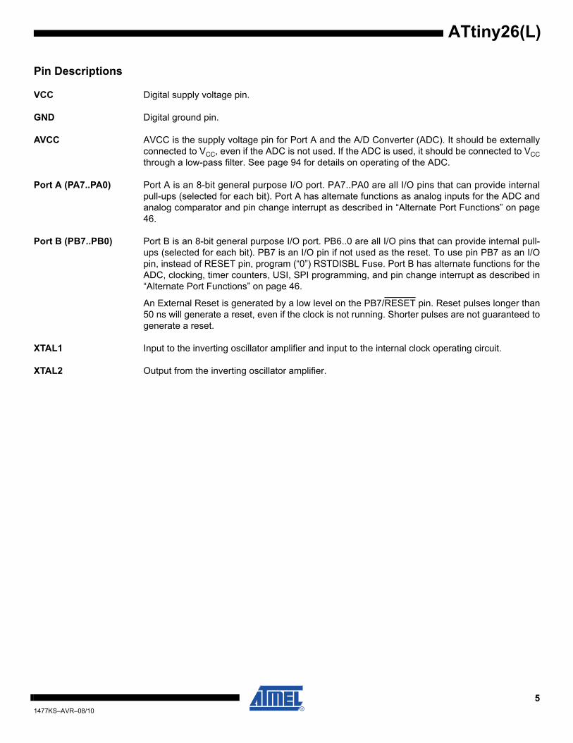
Pin Descriptions
VCC Digital supply voltage pin.
GND Digital ground pin.
AVCC AVCC is the supply voltage pin for Port A and the A/D Converter (ADC). It should be externallyconnected to VCC, even if the ADC is not used. If the ADC is used, it should be connected to VCCthrough a low-pass filter. See page 94 for details on operating of the ADC.
Port A (PA7..PA0) Port A is an 8-bit general purpose I/O port. PA7..PA0 are all I/O pins that can provide internalpull-ups (selected for each bit). Port A has alternate functions as analog inputs for the ADC andanalog comparator and pin change interrupt as described in “Alternate Port Functions” on page46.
Port B (PB7..PB0) Port B is an 8-bit general purpose I/O port. PB6..0 are all I/O pins that can provide internal pull-ups (selected for each bit). PB7 is an I/O pin if not used as the reset. To use pin PB7 as an I/Opin, instead of RESET pin, program (“0”) RSTDISBL Fuse. Port B has alternate functions for theADC, clocking, timer counters, USI, SPI programming, and pin change interrupt as described in“Alternate Port Functions” on page 46.
An External Reset is generated by a low level on the PB7/RESET pin. Reset pulses longer than50 ns will generate a reset, even if the clock is not running. Shorter pulses are not guaranteed togenerate a reset.
XTAL1 Input to the inverting oscillator amplifier and input to the internal clock operating circuit.
XTAL2 Output from the inverting oscillator amplifier.
51477KS–AVR–08/10

General Information
Resources A comprehensive set of development tools, application notes and datasheets are available fordownload on http://www.atmel.com/avr.
Code Examples This datasheet contains simple code examples that briefly show how to use various parts of thedevice. These code examples assume that the part specific header file is included before compi-lation. Be aware that not all C compiler vendors include bit definitions in the header files andinterrupt handling in C is compiler dependent. Please confirm with the C compiler documentationfor more details.
61477KS–AVR–08/10
ATtiny26(L)

ATtiny26(L)
Register SummaryAddress Name Bit 7 Bit 6 Bit 5 Bit 4 Bit 3 Bit 2 Bit 1 Bit 0 Page$3F ($5F) SREG I T H S V N Z C 10$3E ($5E) Reserved$3D ($5D) SP SP7 SP6 SP5 SP4 SP3 SP2 SP1 SP0 11$3C ($5C) Reserved$3B ($5B) GIMSK - INT0 PCIE1 PCIE0 - - - - 58$3A ($5A) GIFR - INTF0 PCIF - - - - - 59$39 ($59) TIMSK - OCIE1A OCIE1B - - TOIE1 TOIE0 - 59$38 ($58) TIFR - OCF1A OCF1B - - TOV1 TOV0 - 60$37 ($57) Reserved$36 ($56) Reserved$35 ($55) MCUCR - PUD SE SM1 SM0 - ISC01 ISC00 37$34 ($54) MCUSR - - - - WDRF BORF EXTRF PORF 36$33 ($53) TCCR0 - - - - PSR0 CS02 CS01 CS00 66$32 ($52) TCNT0 Timer/Counter0 (8-Bit) 67$31 ($51) OSCCAL Oscillator Calibration Register 29$30 ($50) TCCR1A COM1A1 COM1A0 COM1B1 COM1B0 FOC1A FOC1B PWM1A PWM1B 70$2F ($4F) TCCR1B CTC1 PSR1 - - CS13 CS12 CS11 CS10 71$2E ($4E) TCNT1 Timer/Counter1 (8-Bit) 72$2D ($4D) OCR1A Timer/Counter1 Output Compare Register A (8-Bit) 72$2C ($4C) OCR1B Timer/Counter1 Output Compare Register B (8-Bit) 73$2B ($4B) OCR1C Timer/Counter1 Output Compare Register C (8-Bit) 73$2A ($4A) Reserved$29 ($49) PLLCSR - - - - - PCKE PLLE PLOCK$28 ($48) Reserved$27 ($47) Reserved$26 ($46) Reserved$25 ($45) Reserved$24 ($44) Reserved$23 ($43) Reserved$22 ($42) Reserved$21 ($41) WDTCR - - - WDCE WDE WDP2 WDP1 WDP0 78$20 ($40) Reserved$1F ($3F) Reserved$1E ($3E) EEAR - EEAR6 EEAR5 EEAR4 EEAR3 EEAR2 EEAR1 EEAR0 18$1D ($3D) EEDR EEPROM Data Register (8-Bit) 19$1C ($3C) EECR - - - - EERIE EEMWE EEWE EERE 19$1B ($3B) PORTA PORTA7 PORTA6 PORTA5 PORTA4 PORTA3 PORTA2 PORTA1 PORTA0$1A ($3A) DDRA DDA7 DDA6 DDA5 DDA4 DDA3 DDA2 DDA1 DDA0$19 ($39) PINA PINA7 PINA6 PINA5 PINA4 PINA3 PINA2 PINA1 PINA0$18 ($38) PORTB PORTB7 PORTB6 PORTB5 PORTB4 PORTB3 PORTB2 PORTB1 PORTB0$17 ($37) DDRB DDB7 DDB6 DDB5 DDB4 DDB3 DDB2 DDB1 DDB0$16 ($36) PINB PINB7 PINB6 PINB5 PINB4 PINB3 PINB2 PINB1 PINB0$15 ($35) Reserved$14 ($34) Reserved$13 ($33) Reserved$12 ($32) Reserved$11 ($31) Reserved$10 ($30) Reserved$0F ($2F) USIDR Universal Serial Interface Data Register (8-Bit) 81$0E ($2E) USISR USISIF USIOIF USIPF USIDC USICNT3 USICNT2 USICNT1 USICNT0 81$0D ($2D) USICR USISIE USIOIE USIWM1 USIWM0 USICS1 USICS0 USICLK USITC 82$0C ($2C) Reserved$0B ($2)B Reserved$0A ($2A) Reserved$09 ($29) Reserved$08 ($28) ACSR ACD ACBG ACO ACI ACIE ACME ACIS1 ACIS0 91$07 ($27) ADMUX REFS1 REFS0 ADLAR MUX4 MUX3 MUX2 MUX1 MUX0 101$06 ($26) ADCSR ADEN ADSC ADFR ADIF ADIE ADPS2 ADPS1 ADPS0 103$05 ($25) ADCH ADC Data Register High Byte 104$04 ($24) ADCL ADC Data Register Low Byte 104
… Reserved$00 ($20) Reserved
71477KS–AVR–08/10

Instruction Set Summary Mnemonic Operands Description Operation Flags # ClocksARITHMETIC AND LOGIC INSTRUCTIONSADD Rd, Rr Add Two Registers Rd ← Rd + Rr Z,C,N,V,H 1ADC Rd, Rr Add with Carry Two Registers Rd ← Rd + Rr + C Z,C,N,V,H 1ADIW Rdl, K Add Immediate to Word Rdh:Rdl ← Rdh:Rdl + K Z,C,N,V,S 2SUB Rd, Rr Subtract Two Registers Rd ← Rd - Rr Z,C,N,V,H 1SUBI Rd, K Subtract Constant from Register Rd ← Rd - K Z,C,N,V,H 1SBC Rd, Rr Subtract with Carry Two Registers Rd ← Rd - Rr - C Z,C,N,V,H 1SBCI Rd, K Subtract with Carry Constant from Reg. Rd ← Rd - K - C Z,C,N,V,H 1SBIW Rdl, K Subtract Immediate from Word Rdh:Rdl ← Rdh:Rdl - K Z,C,N,V,S 2AND Rd, Rr Logical AND Registers Rd ← Rd • Rr Z,N,V 1ANDI Rd, K Logical AND Register and Constant Rd ← Rd • K Z,N,V 1OR Rd, Rr Logical OR Registers Rd ← Rd v Rr Z,N,V 1ORI Rd, K Logical OR Register and Constant Rd ← Rd v K Z,N,V 1EOR Rd, Rr Exclusive OR Registers Rd ← Rd ⊕ Rr Z,N,V 1COM Rd One’s Complement Rd ← $FF - Rd Z,C,N,V 1NEG Rd Two’s Complement Rd ← $00 - Rd Z,C,N,V,H 1SBR Rd, K Set Bit(s) in Register Rd ← Rd v K Z,N,V 1CBR Rd, K Clear Bit(s) in Register Rd ← Rd • ($FF - K) Z,N,V 1INC Rd Increment Rd ← Rd + 1 Z,N,V 1DEC Rd Decrement Rd ← Rd - 1 Z,N,V 1TST Rd Test for Zero or Minus Rd ← Rd • Rd Z,N,V 1CLR Rd Clear Register Rd ← Rd ⊕ Rd Z,N,V 1SER Rd Set Register Rd ← $FF None 1BRANCH INSTRUCTIONSRJMP k Relative Jump PC ← PC + k + 1 None 2IJMP Indirect Jump to (Z) PC ← Z None 2RCALL k Relative Subroutine Call PC ← PC + k + 1 None 3ICALL Indirect Call to (Z) PC ← Z None 3RET Subroutine Return PC ← STACK None 4RETI Interrupt Return PC ← STACK I 4CPSE Rd, Rr Compare, Skip if Equal if (Rd = Rr) PC ← PC + 2 or 3 None 1/2/3CP Rd, Rr Compare Rd - Rr Z,N,V,C,H 1CPC Rd, Rr Compare with Carry Rd - Rr - C Z,N,V,C,H 1CPI Rd, K Compare Register with Immediate Rd - K Z,N,V,C,H 1SBRC Rr, b Skip if Bit in Register Cleared if (Rr(b) = 0) PC ← PC + 2 or 3 None 1/2/3SBRS Rr, b Skip if Bit in Register is Set if (Rr(b) = 1) PC ← PC + 2 or 3 None 1/2/3SBIC P, b Skip if Bit in I/O Register Cleared if (P(b) = 0) PC ← PC + 2 or 3 None 1/2/3SBIS P, b Skip if Bit in I/O Register is Set if (P(b) = 1) PC ← PC + 2 or 3 None 1/2/3BRBS s, k Branch if Status Flag Set if (SREG(s) = 1) then PC ← PC + k + 1 None 1/2BRBC s, k Branch if Status Flag Cleared if (SREG(s) = 0) then PC ← PC + k + 1 None 1/2BREQ k Branch if Equal if (Z = 1) then PC ← PC + k + 1 None 1/2BRNE k Branch if Not Equal if (Z = 0) then PC ← PC + k + 1 None 1/2BRCS k Branch if Carry Set if (C = 1) then PC ← PC + k + 1 None 1/2BRCC k Branch if Carry Cleared if (C = 0) then PC ← PC + k + 1 None 1/2BRSH k Branch if Same or Higher if (C = 0) then PC ← PC + k + 1 None 1/2BRLO k Branch if Lower if (C = 1) then PC ← PC + k + 1 None 1/2BRMI k Branch if Minus if (N = 1) then PC ← PC + k + 1 None 1/2BRPL k Branch if Plus if (N = 0) then PC ← PC + k + 1 None 1/2BRGE k Branch if Greater or Equal, Signed if (N ⊕ V = 0) then PC ← PC + k + 1 None 1/2BRLT k Branch if Less than Zero, Signed if (N ⊕ V = 1) then PC ← PC + k + 1 None 1/2BRHS k Branch if Half-carry Flag Set if (H = 1) then PC ← PC + k + 1 None 1/2BRHC k Branch if Half-carry Flag Cleared if (H = 0) then PC ← PC + k + 1 None 1/2BRTS k Branch if T-flag Set if (T = 1) then PC ← PC + k + 1 None 1/2BRTC k Branch if T-flag Cleared if (T = 0) then PC ← PC + k + 1 None 1/2BRVS k Branch if Overflow Flag is Set if (V = 1) then PC ← PC + k + 1 None 1/2BRVC k Branch if Overflow Flag is Cleared if (V = 0) then PC ← PC + k + 1 None 1/2BRIE k Branch if Interrupt Enabled if (I = 1) then PC ← PC + k + 1 None 1/2BRID k Branch if Interrupt Disabled if (I = 0) then PC ← PC + k + 1 None 1/2DATA TRANSFER INSTRUCTIONSMOV Rd, Rr Move between Registers Rd ← Rr None 1LDI Rd, K Load Immediate Rd ← K None 1LD Rd, X Load Indirect Rd ← (X) None 2LD Rd, X+ Load Indirect and Post-inc. Rd ← (X), X ← X + 1 None 2LD Rd, -X Load Indirect and Pre-dec. X ← X - 1, Rd ← (X) None 2
81477KS–AVR–08/10
ATtiny26(L)

ATtiny26(L)
LD Rd, Y Load Indirect Rd ← (Y) None 2LD Rd, Y+ Load Indirect and Post-inc. Rd ← (Y), Y ← Y + 1 None 2LD Rd, -Y Load Indirect and Pre-dec. Y ← Y - 1, Rd ← (Y) None 2LDD Rd,Y+q Load Indirect with Displacement Rd ← (Y + q) None 2LD Rd, Z Load Indirect Rd ← (Z) None 2LD Rd, Z+ Load Indirect and Post-inc. Rd ← (Z), Z ← Z + 1 None 2LD Rd, -Z Load Indirect and Pre-dec. Z ← Z - 1, Rd ← (Z) None 2LDD Rd, Z+q Load Indirect with Displacement Rd ← (Z + q) None 2LDS Rd, k Load Direct from SRAM Rd ← (k) None 2ST X, Rr Store Indirect (X) ← Rr None 2ST X+, Rr Store Indirect and Post-inc. (X) ← Rr, X ← X + 1 None 2ST -X, Rr Store Indirect and Pre-dec. X ← X - 1, (X) ← Rr None 2ST Y, Rr Store Indirect (Y) ← Rr None 2ST Y+, Rr Store Indirect and Post-inc. (Y) ← Rr, Y ← Y + 1 None 2ST -Y, Rr Store Indirect and Pre-dec. Y ← Y - 1, (Y) ← Rr None 2STD Y+q, Rr Store Indirect with Displacement (Y + q) ← Rr None 2ST Z, Rr Store Indirect (Z) ← Rr None 2ST Z+, Rr Store Indirect and Post-inc. (Z) ← Rr, Z ← Z + 1 None 2ST -Z, Rr Store Indirect and Pre-dec. Z ← Z - 1, (Z) ← Rr None 2STD Z+q, Rr Store Indirect with Displacement (Z + q) ← Rr None 2STS k, Rr Store Direct to SRAM (k) ← Rr None 2LPM Load Program Memory R0 ← (Z) None 3LPM Rd, Z Load Program Memory Rd ← (Z) None 3IN Rd, P In Port Rd ← P None 1OUT P, Rr Out Port P ← Rr None 1PUSH Rr Push Register on Stack STACK ← Rr None 2POP Rd Pop Register from Stack Rd ← STACK None 2BIT AND BIT-TEST INSTRUCTIONSSBI P, b Set Bit in I/O Register I/O(P,b) ← 1 None 2CBI P, b Clear Bit in I/O Register I/O(P,b) ← 0 None 2LSL Rd Logical Shift Left Rd(n+1) ← Rd(n), Rd(0) ← 0 Z,C,N,V 1LSR Rd Logical Shift Right Rd(n) ← Rd(n+1), Rd(7) ← 0 Z,C,N,V 1ROL Rd Rotate Left through Carry Rd(0) ← C, Rd(n+1) ← Rd(n), C ← Rd(7) Z,C,N,V 1ROR Rd Rotate Right through Carry Rd(7) ← C, Rd(n) ← Rd(n+1), C ← Rd(0) Z,C,N,V 1ASR Rd Arithmetic Shift Right Rd(n) ← Rd(n+1), n = 0..6 Z,C,N,V 1SWAP Rd Swap Nibbles Rd(3..0) ← Rd(7..4), Rd(7..4) ← Rd(3..0) None 1BSET s Flag Set SREG(s) ← 1 SREG(s) 1BCLR s Flag Clear SREG(s) ← 0 SREG(s) 1BST Rr, b Bit Store from Register to T T ← Rr(b) T 1BLD Rd, b Bit Load from T to Register Rd(b) ← T None 1SEC Set Carry C ← 1 C 1CLC Clear Carry C ← 0 C 1SEN Set Negative Flag N ← 1 N 1CLN Clear Negative Flag N ← 0 N 1SEZ Set Zero Flag Z ← 1 Z 1CLZ Clear Zero Flag Z ← 0 Z 1SEI Global Interrupt Enable I ← 1 I 1CLI Global Interrupt Disable I ← 0 I 1SES Set Signed Test Flag S ← 1 S 1CLS Clear Signed Test Flag S ← 0 S 1SEV Set Two’s Complement Overflow V ← 1 V 1CLV Clear Two’s Complement Overflow V ← 0 V 1SET Set T in SREG T ← 1 T 1CLT Clear T in SREG T ← 0 T 1SEH Set Half-carry Flag in SREG H ← 1 H 1CLH Clear Half-carry Flag in SREG H ← 0 H 1NOP No Operation None 1SLEEP Sleep (see specific descr. for Sleep function) None 1WDR Watchdog Reset (see specific descr. for WDR/timer) None 1
Instruction Set Summary (Continued)Mnemonic Operands Description Operation Flags # Clocks
91477KS–AVR–08/10

Notes: 1. This device can also be supplied in wafer form. Please contact your local Atmel sales office for detailed ordering information and minimum quantities.
2. Pb-free packaging alternative, complies to the European Directive for Restriction of Hazardous Substances (RoHS direc-tive). Also Halide free and fully Green.
3. Code Indicators:– U: matte tin– R: tape & reel
Ordering InformationSpeed (MHz) Power Supply (V) Ordering Code(2) Package(2) Operational Range
8 2.7 - 5.5
ATtiny26L-8PUATtiny26L-8SUATtiny26L-8SURATtiny26L-8MUATtiny26L-8MUR
20P320S20S32M1-A32M1-A
Industrial(-40°C to +85°C)(1)
16 4.5 - 5.5
ATtiny26-16PUATtiny26-16SUATtiny26-16SURATtiny26-16MUATtiny26-16MUR
20P320S20S32M1-A32M1-A
Industrial(-40°C to +85°C)(1)
Package Type
20P3 20-lead, 0.300" Wide, Plastic Dual Inline Package (PDIP)
20S 20-lead, 0.300" Wide, Plastic Gull Wing Small Outline (SOIC)
32M1-A 32-pad, 5 x 5 x 1.0 body, Lead Pitch 0.50 mm Quad Flat No-Lead/Micro Lead Frame Package (QFN/MLF)
101477KS–AVR–08/10
ATtiny26(L)

ATtiny26(L)
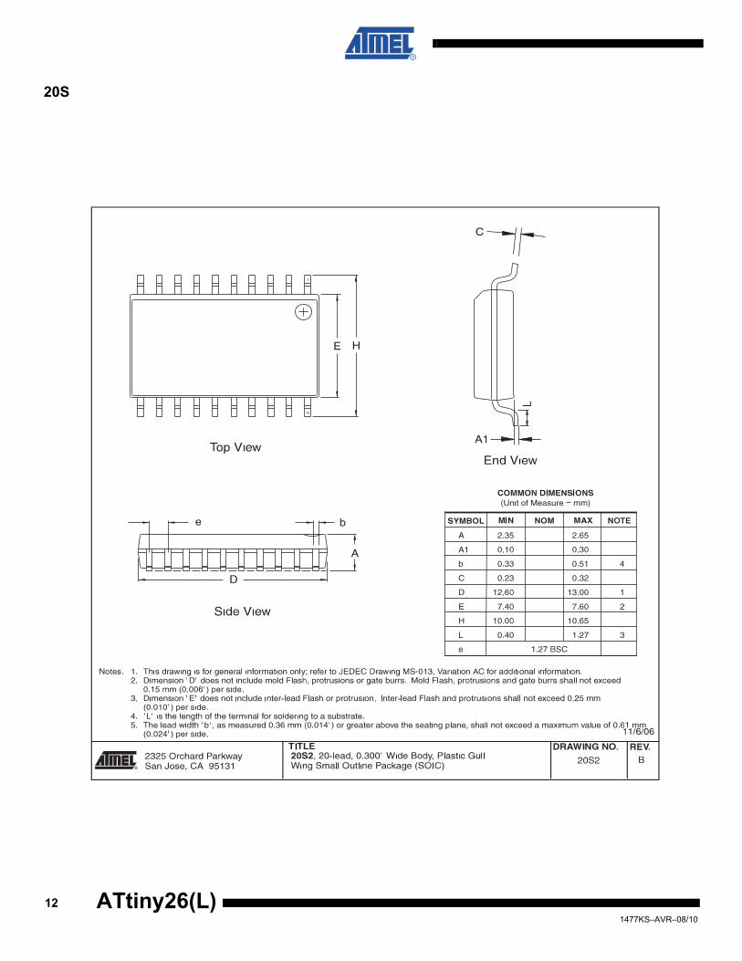
Packaging Information
20P3
2325 Orchard Parkway San Jose, CA 95131
TITLE DRAWING NO.
R
REV. 20P3, 20-lead (0.300"/7.62 mm Wide) Plastic Dual Inline Package (PDIP) C20P3
1/12/04
PIN1
E1
A1
B
E
B1
C
L
SEATING PLANE
A
D
e
eBeC
COMMON DIMENSIONS(Unit of Measure = mm)
SYMBOL MIN NOM MAX NOTE
A – – 5.334
A1 0.381 – –
D 25.493 – 25.984 Note 2
E 7.620 – 8.255
E1 6.096 – 7.112 Note 2
B 0.356 – 0.559
B1 1.270 – 1.551
L 2.921 – 3.810
C 0.203 – 0.356
eB – – 10.922
eC 0.000 – 1.524
e 2.540 TYP
Notes: 1. This package conforms to JEDEC reference MS-001, Variation AD. 2. Dimensions D and E1 do not include mold Flash or Protrusion.
Mold Flash or Protrusion shall not exceed 0.25 mm (0.010").
111477KS–AVR–08/10
20S
121477KS–AVR–08/10
ATtiny26(L)

ATtiny26(L)
32M1-A
2325 Orchard Parkway San Jose, CA 95131
TITLE DRAWING NO.
R
REV. 32M1-A, 32-pad, 5 x 5 x 1.0 mm Body, Lead Pitch 0.50 mm, E32M1-A
5/25/06
3.10 mm Exposed Pad, Micro Lead Frame Package (MLF)
COMMON DIMENSIONS(Unit of Measure = mm)
SYMBOL MIN NOM MAX NOTE
D1
D
E1 E
eb
A3A2
A1 A
D2
E2
0.08 C
L
1
2
3
P
P
01
2
3
A 0.80 0.90 1.00
A1 – 0.02 0.05
A2 – 0.65 1.00
A3 0.20 REF
b 0.18 0.23 0.30
D
D1
D2 2.95 3.10 3.25
4.90 5.00 5.10
4.70 4.75 4.80
4.70 4.75 4.80
4.90 5.00 5.10
E
E1
E2 2.95 3.10 3.25
e 0.50 BSC
L 0.30 0.40 0.50
P – – 0.60
– – 12o
Note: JEDEC Standard MO-220, Fig. 2 (Anvil Singulation), VHHD-2.
TOP VIEW
SIDE VIEW
BOTTOM VIEW
0
Pin 1 ID
Pin #1 Notch(0.20 R)
K 0.20 – –
K
K
131477KS–AVR–08/10

Errata The revision letter refers to the revision of the device.
ATtiny26 Rev. B/C/D
• First Analog Comparator conversion may be delayed
1. First Analog Comparator conversion may be delayedIf the device is powered by a slow rising VCC, the first Analog Comparator conversion willtake longer than expected on some devices.Problem Fix/WorkaroundWhen the device has been powered or reset, disable then enable the Analog Comparatorbefore the first conversion.
141477KS–AVR–08/10
ATtiny26(L)

ATtiny26(L)
Datasheet Revision History
Please note that the referring page numbers in this section refer to the complete document.
Rev. 1477K-08/10 Added tape and reel part numbers in “Ordering Information” on page 171. Removed text“Not recommended for new design” from cover page. Updated last page.
Rev. 1477J-06/07 1. “Not recommended for new design”
Rev. 1477I-05/06 1. Updated “Errata” on page 175
Rev. 1477H-04/06 1. Updated typos.
2. Added “Resources” on page 6.
3. Updated features in “System Control and Reset” on page 32.
4. Updated “Prescaling and Conversion Timing” on page 96.
5. Updated algorithm for “Enter Programming Mode” on page 112.
Rev. 1477G-03/05 1. MLF-package alternative changed to “Quad Flat No-Lead/Micro Lead Frame PackageQFN/MLF”.
2. Updated “Electrical Characteristics” on page 126
3. Updated “Ordering Information” on page 171
Rev. 1477F-12/04 1. Updated Table 16 on page 33, Table 9 on page 28, and Table 29 on page 57.
2. Added Table 20 on page 40.
3. Added “Changing Channel or Reference Selection” on page 98.
4. Updated “Offset Compensation Schemes” on page 105.
5. Updated “Electrical Characteristics” on page 126.
6. Updated package information for “20P3” on page 172.
7. Rearranged some sections in the datasheet.
Rev. 1477E-10/03 1. Removed Preliminary references.
2. Updated “Features” on page 1.
3. Removed SSOP package reference from “Pin Configuration” on page 2.
4. Updated VRST and tRST in Table 16 on page 33.
5. Updated “Calibrated Internal RC Oscillator” on page 29.
151477KS–AVR–08/10

6. Updated DC Characteristics for VOL, IIL, IIH, ICC Power Down and VACIO in “ElectricalCharacteristics” on page 126.
7. Updated VINT, INL and Gain Error in “ADC Characteristics” on page 129 and page 130.Fixed typo in “Absolute Accuracy” on page 130.
8. Added Figure 106 in “Pin Driver Strength” on page 146, Figure 120, Figure 121 andFigure 122 in “BOD Thresholds and Analog Comparator Offset” on page 155. UpdatedFigure 117 and Figure 118.
9. Removed LPM Rd, Z+ from “Instruction Set Summary” on page 169. This instructionis not supported in ATtiny26.
Rev. 1477D-05/03 1. Updated “Packaging Information” on page 172.
2. Removed ADHSM from “ADC Characteristics” on page 129.
3. Added section “EEPROM Write During Power-down Sleep Mode” on page 20.
4. Added section “Default Clock Source” on page 26.
5. Corrected PLL Lock value in the “Bit 0 – PLOCK: PLL Lock Detector” on page 73.
6. Added information about conversion time when selecting differential channels onpage 97.
7. Corrected {DDxn, PORTxn} value on page 42.
8. Added section “Unconnected Pins” on page 46.
9. Added note for RSTDISBL Fuse in Table 50 on page 108.
10. Corrected DATA value in Figure 61 on page 116.
11. Added WD_FUSE period in Table 60 on page 123.
12. Updated “ADC Characteristics” on page 129 and added Table 66, “ADC Characteris-tics, Differential Channels, TA = -40°C to +85°C,” on page 130.
13. Updated “ATtiny26 Typical Characteristics” on page 131.
14. Added LPM Rd, Z and LPM Rd, Z+ in “Instruction Set Summary” on page 169.
Rev. 1477C-09/02 1. Changed the Endurance on the Flash to 10,000 Write/Erase Cycles.
Rev. 1477B-04/02 1. Removed all references to Power Save sleep mode in the section “System Clock andClock Options” on page 23.
2. Updated the section “Analog to Digital Converter” on page 94 with more details onhow to read the conversion result for both differential and single-ended conversion.
3. Updated “Ordering Information” on page 171 and added QFN/MLF packageinformation.
Rev. 1477A-03/02 1. Initial version.
161477KS–AVR–08/10
ATtiny26(L)

ATtiny26(L)
171477KS–AVR–08/10

1477KS–AVR–08/10
Headquarters International
Atmel Corporation2325 Orchard ParkwaySan Jose, CA 95131USATel: 1(408) 441-0311Fax: 1(408) 487-2600
Atmel AsiaUnit 1-5 & 16, 19/FBEA Tower, Millennium City 5418 Kwun Tong RoadKwun Tong, KowloonHong KongTel: (852) 2245-6100Fax: (852) 2722-1369
Atmel EuropeLe Krebs8, Rue Jean-Pierre TimbaudBP 30978054 Saint-Quentin-en-Yvelines CedexFranceTel: (33) 1-30-60-70-00 Fax: (33) 1-30-60-71-11
Atmel Japan9F, Tonetsu Shinkawa Bldg.1-24-8 ShinkawaChuo-ku, Tokyo 104-0033JapanTel: (81) 3-3523-3551Fax: (81) 3-3523-7581
Product Contact
Web Sitewww.atmel.com
Technical SupportEnter Product Line E-mail
Sales Contactwww.atmel.com/contacts
Literature Requestswww.atmel.com/literature
Disclaimer: The information in this document is provided in connection with Atmel products. No license, express or implied, by estoppel or otherwise, to anyintellectual property right is granted by this document or in connection with the sale of Atmel products. EXCEPT AS SET FORTH IN ATMEL’S TERMS AND CONDI-TIONS OF SALE LOCATED ON ATMEL’S WEB SITE, ATMEL ASSUMES NO LIABILITY WHATSOEVER AND DISCLAIMS ANY EXPRESS, IMPLIED OR STATUTORYWARRANTY RELATING TO ITS PRODUCTS INCLUDING, BUT NOT LIMITED TO, THE IMPLIED WARRANTY OF MERCHANTABILITY, FITNESS FOR A PARTICULARPURPOSE, OR NON-INFRINGEMENT. IN NO EVENT SHALL ATMEL BE LIABLE FOR ANY DIRECT, INDIRECT, CONSEQUENTIAL, PUNITIVE, SPECIAL OR INCIDEN-TAL DAMAGES (INCLUDING, WITHOUT LIMITATION, DAMAGES FOR LOSS OF PROFITS, BUSINESS INTERRUPTION, OR LOSS OF INFORMATION) ARISING OUTOF THE USE OR INABILITY TO USE THIS DOCUMENT, EVEN IF ATMEL HAS BEEN ADVISED OF THE POSSIBILITY OF SUCH DAMAGES. Atmel makes norepresentations or warranties with respect to the accuracy or completeness of the contents of this document and reserves the right to make changes to specificationsand product descriptions at any time without notice. Atmel does not make any commitment to update the information contained herein. Unless specifically providedotherwise, Atmel products are not suitable for, and shall not be used in, automotive applications. Atmel’s products are not intended, authorized, or warranted for useas components in applications intended to support or sustain life.
© 2010 Atmel Corporation. All rights reserved. Atmel®, logo and combinations thereof, AVR® and others are registered trademarks or trade-marks of Atmel Corporation or its subsidiaries. Other terms and product names may be trademarks of others.