Embed Size (px)
Citation preview

ATWINC15x0 ATWINC15x0-MR210xB IEEEreg 80211 bgn SmartConnect
IoT Module
Introduction
The ATWINC15x0-MR210xB is a low power consumption 80211 bgn IoT (Internet of Things)modulespecifically optimized for low power IoT applications The module integrates Power Amplifier (PA)Low-Noise Amplifier (LNA) Switch Power Management and a printed antenna or a micro co-ax (uFL)connector for an external antenna resulting in a small form factor (217 x 147 x 21 mm) design It isinteroperable with various vendorsrsquo 80211 bgn access points This module provides SPI ports tointerface with a host controller
The references to the ATWINC15x0-MR210xB module include the module devices listed in the followingbull ATWINC1500-MR210PBbull ATWINC1500-MR210UBbull ATWINC1510-MR210PBbull ATWINC1510-MR210UB
Features
bull IEEEreg 80211 bgn 20 MHz (1x1) solutionbull Single spatial stream in 24 GHz ISM bandbull Integrated TransmitReceive switchbull Integrated PCB antenna or uFL micro co-ax connector for external antennabull Superior sensitivity and range via advanced PHY signal processingbull Advanced equalization and channel estimationbull Advanced carrier and timing synchronizationbull Wi-Fireg Direct (supported till firmware release 1952)bull Soft-AP supportbull Supports IEEE 80211 WEP WPA WPA2 securitybull Superior MAC throughput via hardware accelerated two-level A-MSDUA-MPDU frame aggregation
and block acknowledgmentbull On-chip memory management engine to reduce host loadbull SPI host interfacebull Operating temperature range from -40degC to +85degC RF performance at room temperature of 25oC
with a 2-3 db change at boundary conditionsbull IO operating voltage of 27V to 36Vbull Built-in 26 MHz crystalbull Integrated Flash memory for system software
copy 2017 Microchip Technology Inc Datasheet DS70005304B-page 1
bull Power Save modesndash 4 microA Power-Down mode typical at 33V IOndash 380 microA Doze mode with chip settings preserved (used for beacon monitoring)1
ndash On-chip low power sleep oscillatorndash Fast host wake-up from Doze mode by a pin or SPI transaction
bull Fast Boot optionsndash On-chip boot ROM (Firmware instant boot)ndash SPI flash bootndash Low-leakage on-chip memory for state variablesndash Fast AP re-association (150 ms)
bull On-chip Network stack to offload MCUndash Integrated Network IP stack to minimize host CPU requirementsndash Network features TCP UDP DHCP ARP HTTP TLS and DNSndash Hardware accelerators for Wi-Fi and TLS security to improve connection time
bull Hardware accelerator for IP checksumbull Hardware accelerators for OTA securitybull Small footprint host driverbull Wi-Fi Alliancereg certifications for Connectivity and Optimizations
ndash ID WFA61069
Note For information on module power modes refer to Power Consumption
ATWINC15x0
copy 2017 Microchip Technology Inc Datasheet DS70005304B-page 2
Table of Contents
1 Ordering Information and Module Marking 5
2 Block Diagram 6
3 Pin Description 7
4 Electrical Specifications941 Absolute Maximum Ratings942 Recommended Operating Conditions 9
5 CPU and Memory Subsystems 1051 Processor 1052 Memory Subsystem1053 Non-volatile Memory (eFuse)10
6 WLAN Subsystem 1261 MAC 1262 PHY1363 Radio13
7 External Interfaces1771 Interfacing with the Host Microcontroller 1772 SPI Interface1873 UART Interface20
8 Power Consumption 2281 Description of Device States 2282 Current Consumption in Various Device States 2283 Restrictions for Power States2384 Power-updown Sequence 2385 Digital IO Pin Behavior During Power-up Sequences 2486 Module Reset 25
9 Notes On Interfacing to the ATWINC15x0-MR210xB2691 Programmable Pull Up Resistors 26
10 Schematic Design Information27101 Application Schematic27
11 Module Drawing28111 Module Footprint 29
12 Design Considerations 31121 ATWINC15x0-MR210PB Placement and Routing Guidelines31122 Printed PCB Antenna Performance of ATWINC15x0-MR210PB 31
copy 2017 Microchip Technology Inc Datasheet DS70005304B-page 3
123 ATWINC15x0-MR210UB Placement and Routing Guidelines 34124 Module Assembly Considerations35
13 Reflow Profile Information 36131 Storage Condition36132 Solder Paste36133 Stencil Design 36134 Printing Process 36135 Baking Conditions 36136 Soldering and Reflow Condition37
14 Regulatory Approval39141 United States39142 Canada41143 Europe43144 Other Regulatory Information45
15 Reference Documentation and Support 46151 Reference Documents46
16 Document Revision History 47
The Microchip Web Site 51
Customer Change Notification Service51
Customer Support 51
Microchip Devices Code Protection Feature 51
Legal Notice52
Trademarks 52
Quality Management System Certified by DNV53
Worldwide Sales and Service54
ATWINC15x0
copy 2017 Microchip Technology Inc Datasheet DS70005304B-page 4
1 Ordering Information and Module MarkingFollowing table describes the ordering details for the ATWINC15x0-MR210xB modules
Table 1-1 Ordering Details
Model Number OrderingCode
PackageDimension
NoofPins
Description RegulatoryCertification
ATWINC1500-MR210PB
ATWINC1500-MR210PB1952
217 x 147 x 21mm
28 Certified Module withATWINC1500B chip(4Mb Flash) and PCBprinted antenna
FCC ISEDCE
ATWINC1500-MR210UB
ATWINC1500-MR210UB1952
217 x 147 x 21mm
28 Certified Module withATWINC1500B chip(4Mb Flash) and uFLconnector
FCC ISED
ATWINC1510-MR210PB
ATWINC1510-MR210PB1952
217 x 147 x 21mm
28 Certified Module withATWINC1510B chip(8Mb Flash) and PCBprinted antenna
FCC ISEDCE
ATWINC1510-MR210UB
ATWINC1510-MR210UB1952
217 x 147 x 21mm
28 Certified Module withATWINC1510B chip(8Mb Flash) and uFLconnector
Planned
Following figure illustrates the ATWINC15x0-MR210xB modulesrsquo marking informationFigure 1-1 Marking Information
Module Revision Letter
Software Version
ATWINC15x0 - MR 2 1 0 P
ATWINC1500 4Mb FlashATWINC1510 8Mb Flash
1 No OTA with shield2 OTA with shield
P PCB AntennaU uFL Connector
MR Industrial
Reserved 1 0
ATWINC15x0Ordering Information and Module Marking
copy 2017 Microchip Technology Inc Datasheet DS70005304B-page 5
2 Block DiagramFigure 2-1 ATWINC15x0-MR210xB Module Block Diagram
BALUN
RXTX
26 MHz
GND
SPI_CFG
SPI
GPIO 4
GPIO 5
GPIO 6
IRQNChip_EN
WAKERESET
VBAT VDDIO
GPIO 3
crystal
Printed 24 GHz Antennaor
uFL 24 GHz External Antenna Connector
regWi-Fi
SoCATWINC15x0
ATWINC15x0Block Diagram
copy 2017 Microchip Technology Inc Datasheet DS70005304B-page 6
3 Pin DescriptionFigure 3-1 Pin Diagram
VBAT
GPI
O_1
CHIP
_EN
VDDI
O
1
21 22 23 24 25 26 27 28
1112131415161718
10
19
20
GPI
O_3
GPI
O_4
GPI
O_5
GND
_3
GND_1NCNCNC
NC
RESET_NI2C_SDAI2C_SCLGPIO_6
SPI_CFGWAKE
GND_2IRQN
UART_TXDSPI_MOSISPI_SSN
SPI_MISOSPI_SCK
UART_RXD
1P3V
_TP
234
5
6789
ATWINC15x0-MR210
29 PADDLE
GND (Bottom)
Table 3-1 ATWINC15x0-MR210xB Pin Description
Pin
Name Type Description Programmable Pull Up Resistor
1 GPIO_6 IO General purpose IO Yes
2 I2C_SCL IO I2C Slave Clock Currently used only for developmentdebug Leave unconnected
Yes
3 I2C_SDA IO I2C Slave Data Currently used only for developmentdebug Leave unconnected
Yes
4 RESET_N I Active-Low Hard Reset When this pin is assertedlow the module will be placed in the reset stateWhen this pin is asserted high the module will be outof reset and will function normally Connect to a hostoutput that defaults low at power up If the host outputis tri-stated add a 1MΩ pull down resistor to ensure alow level at power-up
No
5 NC - No connect
ATWINC15x0Pin Description
copy 2017 Microchip Technology Inc Datasheet DS70005304B-page 7
Pin
Name Type Description Programmable Pull Up Resistor
6 NC - No connect
7 NC - No connect
8 NC - No connect
9 GND_1 - GND
10 SPI_CFG I Tie to VDDIO through a 1MΩ resistor to enable theSPI interface
No
11 WAKE I Host Wake control Can be used to wake-up themodule from Doze mode Connect to a host GPIO
Yes
12 GND_2 - GND
13 IRQN O ATWINC15x0-MR210xB Device Interrupt outputConnect to host interrupt input pin
Yes
14 UART_TXD O UART Transmit Output from ATWINC15x0-MR210xBAdded debug
Yes
15 SPI_RXD I SPI MOSI (Master Out Slave In) pin Yes
16 SPI_SSN I SPI Slave Select Active-low Yes
17 SPI_TXD O SPI MISO (Master In Slave Out) pin Yes
18 SPI_SCK I SPI Clock Yes
19 UART_RXD I UART Receive input to ATWINC15x0-MR210xBAdded debug
Yes
20 VBATT - Battery power supply
21 GPIO_1RTC I General Purpose IO RTC Yes
22 CHIP_EN I Module enable High level enables the module lowlevel places module in Power-Down mode Connectto a host output that defaults low at power-up If thehost output is tri-stated add a 1MΩ pull down resistorto ensure a low level at power-up
No
23 VDDIO - IO Power Supply Must match host IO voltage
24 1P3V_TP - 13V VDD Core Test Point Decouple with 10microF and001microF to GND
25 GPIO_3 IO General purpose IO
26 GPIO_4 IO General purpose IO Yes
27 GPIO_5 IO General purpose IO Yes
28 GND_3 - GND
29 PADDLE GND - GND
ATWINC15x0Pin Description
copy 2017 Microchip Technology Inc Datasheet DS70005304B-page 8
4 Electrical Specifications
41 Absolute Maximum RatingsAbsolute maximum ratings for the ATWINC15x0-MR210xB modules are listed below
Table 4-1 Conditions
Symbol Description Min Max Unit
VBATT Input supply voltage -03 50 V
VDDIO IO voltage -03 42 V
Operating Temperature -40 +85 oC
CAUTION Stresses listed under Absolute Maximum Ratings may cause permanent damage to thedevice This is a stress rating only The functional operation of the device at those or any otherconditions above those indicated in the operation listings of this specification is not impliedExposure to maximum rating conditions for extended periods may affect the device reliability
42 Recommended Operating ConditionsTable 4-2 Recommended Operating Conditions
Symbol Min Typ Max Unit
VBATT 30 33 42 V
VDDIO 27 33 36 V
Note 1 Test Conditions -40oC - +85oC
ATWINC15x0Electrical Specifications
copy 2017 Microchip Technology Inc Datasheet DS70005304B-page 9
5 CPU and Memory Subsystems
51 ProcessorThe ATWINC15x0-MR210xB modules have a Cortus APS3 32-bit processor This processor performsmany of the MAC functions including but not limited to the association authentication powermanagement security key management and MSDU aggregationde-aggregation In addition theprocessor provides flexibility for various modes of operation such as STA and AP modes
52 Memory SubsystemThe APS3 core uses a 128KB instructionboot ROM along with a 160KB instruction RAM and a 64KBdata RAM The ATWINC15x0-MR210xB modules come populated with either 4Mb or 8Mb of Flashmemory depending on the module model that is ordered This memory can be used for system softwareSee Table 1-1 for more information In addition the device uses a 128KB shared RAM accessible by theprocessor and MAC which allows the APS3 core to perform various data management tasks on the TXand RX data packets
53 Non-volatile Memory (eFuse)The ATWINC15x0-MR210xB modules have 768 bits of non-volatile eFuse memory that can be read bythe CPU after device reset This non-volatile one-time-programmable (OTP) memory can be used to storecustomer-specific parameters such as MAC address various calibration information such as TX powercrystal frequency offset etc and other software-specific configuration parameters The eFuse ispartitioned into six 128-bit banks Each bank has the same bitmap (see following figure) The purpose ofthe first 80 bits in each bank is fixed and the remaining 48 bits are general-purpose software dependentbits or reserved for future use Since each bank can be programmed independently this allows forseveral updates of the device parameters following the initial programming for example if the MACaddress has to be changed Bank 1 has to be programmed with the new MAC address along with thevalues of TX gain correction and frequency offset if they are used and programmed in Bank 0 Thecontents of Bank 0 have to be invalidated in this case by programming the invalid bit in the Bank 0 Thiswill allow the firmware to use the MAC address By default all the ATWINC15x0-MR210xB modules areprogrammed with the MAC address and the frequency offset bits of Bank 0
ATWINC15x0CPU and Memory Subsystems
copy 2017 Microchip Technology Inc Datasheet DS70005304B-page 10
Figure 5-1 eFuse Bitmap
Bank 0
Bank 1
Bank 2
Bank 3
Bank 4
Bank 5
F MAC ADDR
Used
Inva
lid
Version
Reserved
MAC
ADDR
Used
FO
Flags
G
31 1 4 1
Used TX Gain
Correc
tion
Used
Freq
Offs
et
1 7
488 8 16
1 15
128 Bits
ATWINC15x0CPU and Memory Subsystems
copy 2017 Microchip Technology Inc Datasheet DS70005304B-page 11
6 WLAN SubsystemThe WLAN subsystem is composed of the Media Access Controller (MAC) and the Physical Layer (PHY)The following two subsections describe the MAC and PHY in detail
61 MAC
611 DescriptionThe ATWINC15x0-MR210xB MAC is designed to operate at low power while providing high datathroughput The IEEE 80211 MAC functions are implemented with a combination of dedicated datapathengines hardwired control logic and a low-power high-efficiency microprocessor The combination ofdedicated logic with a programmable processor provides optimal power efficiency and real-time responsewhile providing the flexibility to accommodate evolving standards and future feature enhancements
Dedicated datapath engines are used to implement datapath functions with heavy computationalrequirements For example an FCS engine checks the CRC of the transmitting and receiving packetsand a cipher engine performs all the required encryption and decryption operations for the WEP WPA-TKIP and WPA2 CCMP-AES
Control functions which have real-time requirements are implemented using hardwired control logicmodules These logic modules offer real-time response while maintaining configurability via theprocessor Examples of hardwired control logic modules are the channel access control module(implements EDCAHCCA Beacon TX control interframe spacing etc) protocol timer module(responsible for the Network Access Vector back-off timing timing synchronization function and slotmanagement) MPDU handling module aggregationde-aggregation module block ACK controller(implements the protocol requirements for burst block communication) and TXRX control FSMs(coordinate data movement between PHY-MAC interface cipher engine and the DMA interface to theTXRX FIFOs)
The MAC functions implemented solely in software on the microprocessor have the followingcharacteristics
bull Functions with high memory requirements or complex data structures Examples are associationtable management and power save queuing
bull Functions with low computational load or without critical real-time requirements Examples areauthentication and association
bull Functions which need flexibility and upgradeability Examples are beacon frame processing andQoS scheduling
612 FeaturesThe ATWINC15x0-MR210xB IEEE80211 MAC supports the following functions
bull IEEE 80211bgnbull IEEE 80211e WMM QoS EDCAPCF multiple access categories traffic schedulingbull Advanced IEEE 80211n features
ndash Transmission and reception of aggregated MPDUs (A-MPDU)ndash Transmission and reception of aggregated MSDUs (A-MSDU)ndash Immediate Block Acknowledgmentndash Reduced Interframe Spacing (RIFS)
ATWINC15x0WLAN Subsystem
copy 2017 Microchip Technology Inc Datasheet DS70005304B-page 12
bull Support for IEEE80211i and WFA security with key managementndash WEP 64128ndash WPA-TKIPndash 128-bit WPA2 CCMP (AES)
bull Advanced power managementndash Standard 80211 Power Save Mode
bull RTS-CTS and CTS-self supportbull Supports either STA or AP mode in the infrastructure basic service set mode
62 PHY
621 DescriptionThe ATWINC1500B WLAN PHY is designed to achieve reliable and power-efficient physical layercommunication specified by IEEE 80211 bgn in single stream mode with 20MHz bandwidth Advancedalgorithms have been employed to achieve maximum throughput in a real world communicationenvironment with impairments and interference The PHY implements all the required functions thatinclude FFT filtering FEC (Viterbi decoder) frequency timing acquisition and tracking channelestimation and equalization carrier sensing clear channel assessment and automatic gain control
622 FeaturesThe ATWINC1500B IEEE80211 PHY supports the following functions
bull Single antenna 1x1 stream in 20MHz channelsbull Supports IEEE 80211b DSSS-CCK modulation 1 2 55 11Mbpsbull Supports IEEE 80211g OFDM modulation 6 9 1218 24 36 48 54Mbpsbull Supports IEEE 80211n HT modulations MCS0-7 20MHz 800 and 400ns guard interval 65 72
130 144 195 217 260 289 390 433 520 578 585 650 722Mbpsbull IEEE 80211n mixed mode operationbull Per packet TX power controlbull Advanced channel estimationequalization automatic gain control CCA carriersymbol recovery
and frame detection
63 RadioThis section presents information describing the properties and characteristics of the ATWINC15x0-MR210xB and Wi-Fi radio transmit and receive performance capabilities of the device
The performance measurements are taken at the RF pin assuming 50Ω impedance the RF performanceis guaranteed for room temperature of 25oC with a derating of 2-3dB at boundary conditions
Measurements were taken under typical conditions VBATT=33V VDDIO=33V temperature +25ordmC
Table 6-1 Features and Properties
Feature Description
Part Number ATWINC15x0-MR210xB
WLAN Standard IEEE 80211 bgn Wi-Fi compliant
ATWINC15x0WLAN Subsystem
copy 2017 Microchip Technology Inc Datasheet DS70005304B-page 13
Feature Description
Host Interface SPI
Dimension 217 x 147 x 21 mm
Frequency Range 2412GHz ~ 2472GHz (24GHz ISM Band)
Number of Channels 11 for North America and 13 for Europe
Modulation 80211b DQPSK DBPSK CCK80211gn OFDM 64-QAM16-QAM QPSK BPSK
Data Rate 80211b 1 2 55 11Mbps
80211g 6 9 12 18 24 36 48 54Mbps
Data Rate(20MHz normal GI 800ns)
80211n 65 13 195 26 39 52 585 65Mbps
Data Rate(20MHz short GI 400ns)
80211n 72 144 217 289 433 57865722Mbps
Operating temperature -40 to +85oC
Storage temperature -40 to +125 oC
Humidity Operating Humidity 10 to 95 Non-CondensingStorage Humidity 5 to 95 Non-Condensing
631 Receiver PerformanceTable 6-2 Receiver Performance
Parameter Description Minimum Typical Maximum Unit
Frequency 2412 2472 MHz
Sensitivity80211b
1Mbps DSS -95
dBm
2Mbps DSS -90
55Mbps DSS -92
11Mbps DSS -86
Sensitivity80211g
6Mbps OFDM -90
9Mbps OFDM -89
12Mbps OFDM -88
18Mbps OFDM -85
24Mbps OFDM -83
36Mbps OFDM -80
48Mbps OFDM -76
54Mbps OFDM -74
ATWINC15x0WLAN Subsystem
copy 2017 Microchip Technology Inc Datasheet DS70005304B-page 14
Parameter Description Minimum Typical Maximum Unit
Sensitivity80211n(BW=20MHz)
MCS 0 -89
MCS 1 -87
MCS 2 -85
MCS 3 -82
MCS 4 -77
MCS 5 -74
MCS 6 -72
MCS 7 -705
Maximum ReceiveSignal Level
1-11Mbps DSS 0
6-54Mbps OFDM 0
MCS 0 ndash 7 0
Adjacent Channel Rejection
1Mbps DSS (30MHz offset) 50
dB
11Mbps DSS (25MHz offset) 43
6Mbps OFDM (25MHz offset) 40
54Mbps OFDM (25MHz offset) 25
MCS 0 ndash 20MHz BW (25MHz offset) 40
MCS 7 ndash 20MHz BW (25MHz offset) 20
Cellular Blocker Immunity
776-794MHz CDMA -14
dBm
824-849MHz GSM -10
880-915MHz GSM -10
1710-1785MHz GSM -15
1850-1910MHz GSM -15
1850-1910MHz WCDMA -24
1920-1980MHz WCDMA -24
632 Transmitter PerformanceTable 6-3 Transmitter Performance
Parameter Description Minimum Typical Maximum Unit
Frequency mdash 2412 mdash 2472 MHz
Output Power1-2
ON_Transmit
80211b 1Mbps mdash 175 mdash
dBm80211b 11Mbps mdash 185 mdash
80211g 6Mbps mdash 175 mdash
80211g 54Mbps mdash 16 mdash
ATWINC15x0WLAN Subsystem
copy 2017 Microchip Technology Inc Datasheet DS70005304B-page 15
Parameter Description Minimum Typical Maximum Unit
80211n MCS 0 mdash 170 mdash
80211n MCS 7 mdash 145 mdash
TX Power Accuracy mdash mdash plusmn15 2 mdash dB
Carrier Suppression mdash mdash 300 mdash dBc
Harmonic Output Power2nd mdash -41
dBmMHz3rd mdash mdash -41
Note 1 Measured at 80211 spec compliant EVMSpectral Mask2 Measured after RF matching network3 Operating temperature range is -40degC to +85degC RF performance guaranteed at room temperature
of 25degC with a 2-3dB change at boundary conditions 4 With respect to TX power different (higherlower) RF output power settings may be used for
specific antennas andor enclosures in which case recertification may be required5 The availability of some specific channels andor operational frequency bands are country
dependent and should be programmed at the Host product factory to match the intendeddestination Regulatory bodies prohibit exposing the settings to the end user This requirementneeds to be taken care of via Host implementation
ATWINC15x0WLAN Subsystem
copy 2017 Microchip Technology Inc Datasheet DS70005304B-page 16
7 External Interfaces
71 Interfacing with the Host MicrocontrollerThis section describes interfacing the ATWINC15x0-MR210xB module with the host microcontroller Theinterface is comprised of a slave SPI and additional control signals as shown in the following figure Formore information on SPI interface specification and timing refer to the SPI Interface Additional controlsignals are connected to the GPIOIRQ interface of the microcontroller
Figure 7-1 Interfacing with Host Microcontroller
Host Microcontroller
CHIP_EN
RESET
WAKE
IRQN
SPI Wi-Fi Controller
Module
Table 7-1 Host Microcontroller Interface Pins
Pin Number Function
4 RESET_N
11 WAKE
13 IRQ_N
22 CHIP_EN
16 SPI_SSN
15 SPI_MOSI
17 SPI_MISO
18 SPI_SCK
Related LinksSPI Interface
ATWINC15x0External Interfaces
copy 2017 Microchip Technology Inc Datasheet DS70005304B-page 17
72 SPI Interface
721 OverviewThe ATWINC15x0-MR210xB has a Serial Peripheral Interface (SPI) that operates as an SPI slave TheSPI interface can be used for control and for serial IO of 80211 data The SPI pins are mapped asshown in the following table The SPI is a full-duplex slave-synchronous serial interface that is availableimmediately following reset when pin 10 (SPI_CFG) is tied to VDDIO
Table 7-2 SPI Interface Pin Mapping
Pin SPI function
10 CFG Must be tied to VDDIO
16 SSN Active-Low Slave Select
15 MOSI(RXD) Serial Data Receive
18 SCK Serial Clock
17 MISO(TXD) Serial Data Transmit
When the SPI is not selected that is when SSN is high the SPI interface will not interfere with datatransfers between the serial-master and other serial-slave devices When the serial slave is not selectedits transmitted data output is buffered resulting in a high impedance drive onto the MISO line
The SPI interface responds to a protocol that allows an external host to read or write any register in thechip as well as initiate DMA transfers
The SPI SSN MOSI MISO and SCK pins of the ATWINC15x0-MR210xB have internal programmablepull-up resistors These resistors should be programmed to be disabled otherwise if any of the SPI pinsare driven to a low level while the ATWINC15x0-MR210xB is in the low power sleep state the current willflow from the VDDIO supply through the pull-up resistors increasing the current consumption of themodule
Related LinksProgrammable Pull Up Resistors
722 SPI TimingThe SPI Slave interface supports four standard modes as determined by the Clock Polarity (CPOL) andClock Phase (CPHA) settings These modes are illustrated in the following table and figure
Table 7-3 SPI Slave Modes
Mode CPOL CPHA
0 0 0
1 0 1
2 1 0
3 1 1
The red lines in the following figure correspond to Clock Phase = 0 and the blue lines correspond to ClockPhase = 1
ATWINC15x0External Interfaces
copy 2017 Microchip Technology Inc Datasheet DS70005304B-page 18
Figure 7-2 SPI Slave Clock Polarity and Clock Phase Timing
z
z z
z
SCKCPOL = 0
CPOL = 1
SSN
RXDTXD(MOSIMISO)
CPHA = 0
CPHA = 1
2 3 4 5 6 7 8
1 2 3 4 5 6 7
1
8
The SPI timing is provided in the following figure and table
Figure 7-3 SPI Timing Diagram (SPI Mode CPOL=0 CPHA=0)
t LH
SCK
TXD
RXD
t WH
t HL
t WL
t ODLY
t ISU t IHD
f SCK
SSN
t SUSSN t HDSSN
Table 7-4 SPI Slave Timing Parameters1
Parameter Symbol Min Max Units
Clock Input Frequency2 fSCK mdash 48 MHz
Clock Low Pulse Width tWL 4 mdash
nsClock High Pulse Width tWH 5 mdash
Clock Rise Time tLH 0 7
Clock Fall Time tHL 0 7
ATWINC15x0External Interfaces
copy 2017 Microchip Technology Inc Datasheet DS70005304B-page 19
Parameter Symbol Min Max Units
TXD Output Delay3 tODLY 4 9 from SCK fall125 from SCKrise
RXD Input Setup Time tISU 1 mdash
RXD Input Hold Time tIHD 5 mdash
SSN Input Setup Time tSUSSN 3 mdash
SSN Input Hold Time tHDSSN 55 mdash
Note 1 Timing is applicable to all SPI modes2 Maximum clock frequency specified is limited by the SPI Slave interface internal design actual
maximum clock frequency can be lower and depends on the specific PCB layout3 Timing based on 15pF output loading
73 UART InterfaceThe ATWINC15x0-MR210xB supports the Universal Asynchronous ReceiverTransmitter (UART)interface This interface should be used for debug purposes only The UART is available on pins 14 and19 The UART is compatible with the RS-232 standard and the ATWINC15x0-MR210xB operates asData Terminal Equipment (DTE) It has a two-pin RXDTXD interface
The default configuration for accessing the UART interface of ATWINC15x0-MR210xB is mentionedbelow
bull Baud rate 115200bull Data 8 bitbull Parity Nonebull Stop bit 1 bitbull Flow control None
It also has RX and TX FIFOs which ensure reliable high-speed reception and low software overheadtransmission FIFO size is 4 x 8 for both RX and TX direction The UART also has status registersshowing the number of received characters available in the FIFO and various error conditions as well theability to generate interrupts based on these status bits
An example of the UART receiving or transmitting a single packet is shown in the following figure Thisexample shows 7-bit data (0x45) odd parity and two stop bits
Important UART2 supports RTS and CTS flow control The UART RTS and UART CTSMUST be connected to the host MCU UART and enabled for the UART interface to befunctional
ATWINC15x0External Interfaces
copy 2017 Microchip Technology Inc Datasheet DS70005304B-page 20
Figure 7-4 Example of UART RX of TX Packet
Previous Packets or
Leading Idle Bits
Current Packet
DataStart Bit
Parity Bit Stop Bits
Next Packet
ATWINC15x0External Interfaces
copy 2017 Microchip Technology Inc Datasheet DS70005304B-page 21
8 Power Consumption
81 Description of Device StatesThe ATWINC15x0-MR210xB has several device states
bull ON_Transmit ndash Device is actively transmitting an 80211 signal Highest output power and nominalcurrent consumption
bull ON_Receive ndash Device is actively receiving an 80211 signal Lowest sensitivity and nominal currentconsumption
bull ON_Doze ndash Device is ON but is neither transmitting nor receivingbull Power_Down ndash Device core supply off (Leakage)bull IDLE connect ndash Device is connected with 1 DTIM beacon interval
The following pins are used to switch between the ON and Power_Down states
bull CHIP_EN ndash Device pin (pin 22) used to enable DCDC Converterbull VDDIO ndash IO supply voltage from external supply
In the ON states VDDIO is on and CHIP_EN is high (at VDDIO voltage level) To switch betweenthe ON states and Power_Down state CHIP_EN has to change between high and low (GND)voltage When VDDIO is off and CHIP_EN is low the chip is powered off with no leakage (also see Restrictions for Power States)
82 Current Consumption in Various Device StatesTable 8-1 Current Consumption
Device State Code Rate Outputpower dBm
Current Consumption 1
IVBATT IVDDIO
ON_Transmit
80211b 1Mbps 175 268mA 22mA
80211b 11Mbps 185 264mA 22mA
80211g 6Mbps 175 269mA 22mA
80211g 54Mbps 160 266mA 22mA
80211n MCS 0 170 268mA 22mA
80211n MCS 7 145 265mA 22mA
ON_Receive
80211b 1Mbps NA 61mA 22mA
80211b 11Mbps NA 61mA 22mA
80211g 6Mbps NA 61mA 22mA
80211g 54Mbps NA 61mA 22mA
80211n MCS 0 NA 61mA 22mA
80211n MCS 7 NA 61mA 22mA
ATWINC15x0Power Consumption
copy 2017 Microchip Technology Inc Datasheet DS70005304B-page 22
Device State Code Rate Outputpower dBm
Current Consumption 1
IVBATT IVDDIO
ON_Doze NA NA 380microA lt10microA
Power_Down NA NA lt05microA lt35microA
Note
1 Measured conditions VBATT 33V VDDIO 33V temp 25degC
83 Restrictions for Power StatesWhen no power is supplied to the device for example the DCDC Converter output and VDDIO are bothoff (at ground potential) a voltage cannot be applied to the device pins because each pin contains anESD diode from the pin to supply This diode will turn on when a voltage higher than one diode drop issupplied to the pin
If a voltage must be applied to the signal pads while the chip is in a low-power state the VDDIO supplymust be on so the SLEEP or Power_Down state must be used
Similarly to prevent the pin-to-ground diode from turning on do not apply a voltage that is more than onediode drop below ground to any pin
84 Power-updown SequenceThe power-updown sequence for ATWINC15x0-MR210xB is shown in the Following Figure The timingparameters are provided in following the table
Figure 8-1 Power UpDown Sequence
VBATT
VDDIO
CHIP_EN
RESETN
t A
t B
t C
XO Clock
t B
t A
tC
Table 8-2 Power-updown Sequence Timing
Parameter Min Max Units Description Notes
tA0 ms VBATT rise to VDDIO
riseVBATT and VDDIO can risesimultaneously or can be tied
ATWINC15x0Power Consumption
copy 2017 Microchip Technology Inc Datasheet DS70005304B-page 23
Parameter Min Max Units Description Notes
together VDDIO must not risebefore VBATT
tB0 ms VDDIO rise to CHIP_EN
riseCHIP_EN must not rise beforeVDDIO CHIP_EN must be drivenhigh or low not left floating
tC
5 ms CHIP_EN rise toRESETN rise
This delay is needed because theXO clock must stabilize beforeRESETN removal RESETN mustbe driven high or low not leftfloating
tArsquo
0 ms VDDIO fall to VBATT fall VBATT and VDDIO can fallsimultaneously or can be tiedtogether VBATT must not fallbefore VDDIO
tBrsquo
0 ms CHIP_EN fall to VDDIOfall
VDDIO must not fall beforeCHIP_EN CHIP_EN and RESETNcan fall simultaneously
tCrsquo
0 ms RESETN fall to VDDIOfall
VDDIO must not fall beforeRESETN RESETN and CHIP_ENcan fall simultaneously
85 Digital IO Pin Behavior During Power-up SequencesThe following table represents digital IO Pin states corresponding to device power modes
Table 8-3 Digital IO Pin Behavior in Different Device States
Device state VDDIO CHIP_EN RESETN Outputdriver
Inputdriver
Pull updownresistor (96kΩ)
Power-Downcore supply off
High Low Low Disabled (Hi-Z) Disabled Disabled
Power-on Resetcore supply on hard reseton
High High Low Disabled (Hi-Z) Disabled Enabled
Power-On Defaultcore supply on the deviceis out of reset but notprogrammed yet
High High High Disabled (Hi-Z) Enabled Enabled
On SleepOn TransmitOn Receivecore supply on deviceprogrammed by firmware
High High High Programmed byfirmware foreach pinEnabled orDisabled
Oppositeof OutputDriverstate
Programmed byfirmware foreach pinEnabled orDisabled
ATWINC15x0Power Consumption
copy 2017 Microchip Technology Inc Datasheet DS70005304B-page 24
86 Module ResetIf a module reset is performed the RESETN pin must be pulsed low for a minimum of 1micro second
ATWINC15x0Power Consumption
copy 2017 Microchip Technology Inc Datasheet DS70005304B-page 25
9 Notes On Interfacing to the ATWINC15x0-MR210xB
91 Programmable Pull Up ResistorsThe ATWINC15x0-MR210xB provides programmable pull up resistors on various pins The purpose ofthese resistors is to keep any unused input pins from floating which can cause excess current to flowthrough the input buffer from the VDDIO supply Any unused module pin on the ATWINC15x0-MR210xBshould leave these pull up resistors enabled so the pin will not float The default state at power-up is forthe pull up resistor to be enabled However any pin that is used should have the pull up resistor disabledThe reason for this is that if any pins are driven to a low level while the ATWINC15x0-MR210xB is in thelow power sleep state current will flow from the VDDIO supply through the pull up resistors increasingthe current consumption of the module Since the value of the pull up resistor is approximately 100KΩthe current through any pull up resistor that is being driven low will be VDDIO100K For VDDIO = 33Vthe current through each pull up resistor that is driven low would be approximately 33V100K = 33microAPins which are used and have had the programmable pull up resistor disabled should always be activelydriven to either a high or low level and not be allowed to float
ATWINC15x0Notes On Interfacing to the ATWINC15x0-MR210xB
copy 2017 Microchip Technology Inc Datasheet DS70005304B-page 26
10 Schematic Design InformationThis section provides schematic information for reference Application schematics for SPI are provided inthe following figure Module design information such as module schematics can be obtained under anNDA from Microchip These schematics are applicable to the ATWINC1500-MR210PB ATWINC1510-MR210PB and the ATWINC1500-MR210UB modules
101 Application SchematicFigure 10-1 SPI Application Schematic
Resistors R2-R1 are recommendedAs placeholders in case filteringof noisy signals is required Theyalso allow disconnecting of module For debug purposes
Note Add 10uF and 001uF decoupling capacitors between the pin 24 (1P3V_TP) and GND
ATWINC15x0Schematic Design Information
copy 2017 Microchip Technology Inc Datasheet DS70005304B-page 27
11 Module DrawingThis section provides information about the module package outline drawings
Figure 11-1 Module Drawing - ATWINC15x0-MR210PB (unit = mm)
MODULE TOP VIEW
Metal Shield
Metal Shield
PCB
MODULE SIDE VIEW MODULE BOTTOM VIEW
NOTE THIS PAD MUST BE SOLDERED TO GND
NOT TO SCALE
ATWINC15x0Module Drawing
copy 2017 Microchip Technology Inc Datasheet DS70005304B-page 28
Figure 11-2 Module Drawings ndash ATWINC15x0-MR210UB (unit = mm)
MODULE TOP VIEW
Metal Shield
Metal Shield
PCB
MODULE SIDE VIEW MODULE BOTTOM VIEW
NOTE THIS PAD MUST BE SOLDERED TO GND
NOT TO SCALE Rev 2
111 Module FootprintThis section provides the outline drawing for the recommended footprint for the ATWINC15x0-MR210xBmodule It is imperative that the center Ground Pad is provided with an array of vias to provide for a goodground and thermal transfer for the ATWINC15x0-MR210xB module
This footprint is applicable to the ATWINC15x0-MR210xB module devices
ATWINC15x0Module Drawing
copy 2017 Microchip Technology Inc Datasheet DS70005304B-page 29
Figure 11-3 Module Solder Pad Footprint (unit = mm)
NOTE THIS PAD MUST BE TIED TO GND
1016 Pitch
1473
19
08
1016 Pitch
4064
267
267
600
1016 Pitch
370
370
1016 Pitch
19 3048
368
2172 2032
442
SOLDER PAD FOOTPRINT
Drawing not to scaleUntoleranced dimensionsUnits=mm
ATWINC15x0Module Drawing
copy 2017 Microchip Technology Inc Datasheet DS70005304B-page 30
12 Design ConsiderationsThis section provides the guidelines on placement and routing to achieve the best performance
121 ATWINC15x0-MR210PB Placement and Routing Guidelinesbull The module must be placed on the main board ndash the printed antenna area must overlap with the
carrier board The portion of the module containing the antenna should not go outside the edge ofthe main board The antenna is designed to work properly when it is sitting directly on top of a15mm thick printed circuit board
bull If the module is placed at the edge of the main board a minimum 22mm by 5mm area directlyunder the antenna must be clear of all metal on all layers of the board ldquoIn-landrdquo placement isacceptable however deepness of keep-out area must grove to module edge to main board edgeplus 5mm DO NOT PLACE THE MODULE IN THE MIDDLE OF THE MAIN BOARD OR FARAWAY FROM THE MAIN BOARD EDGE
bull Keep away from the antenna as far as possible large metal objects to avoid electromagnetic fieldblocking
bull Do not enclose the antenna within a metal shieldbull Keep any components which may radiate noise or signals within the 24GHz-25GHz frequency
band as far away from the antenna as possible or better yet shield those components Any noiseradiated from the main board in this frequency band will degrade the sensitivity of the module
Figure 12-1 ATWINC15x0-MR210PB Placement Reference
Best Case
Worst Case
System Ground Plane
(a)
(b)
Keep out area
Microchip
Microchip
122 Printed PCB Antenna Performance of ATWINC15x0-MR210PBThe printed PCB antenna on the ATWINC15x0-MR210PB is a meandered Inverted F Antenna (IFA) Theantenna is fed via matching network which is matched for the module installed on a 15mm thick main
ATWINC15x0Design Considerations
copy 2017 Microchip Technology Inc Datasheet DS70005304B-page 31
board Main board thickness deviation by plusmn1mm changes RXTX performance by plusmn1dB maximumreferring to RXTX performance with a default antenna matching network and installed on 15mm thickmain board
Measured peak antenna gain is -03dBi
Antenna Radiation PatternFollowing figures illustrate the Antenna Radiation PatternsFigure 12-2 Antenna Radiation Pattern when Phi = 0 degree
ATWINC15x0Design Considerations
copy 2017 Microchip Technology Inc Datasheet DS70005304B-page 32
Figure 12-3 Antenna Radiation Pattern when Phi = 90 degree
ATWINC15x0Design Considerations
copy 2017 Microchip Technology Inc Datasheet DS70005304B-page 33
Figure 12-4 Antenna Radiation Pattern when Theta = 90 degree
123 ATWINC15x0-MR210UB Placement and Routing GuidelinesThe ATWINC15x0-MR210UB module has an Ultra Small Miniature RF Connector (uFL) for the externalantenna
The choice of antenna is limited to the antenna types for which the module was tested and approved Fora list of tested and approved antennas that may be used with the module refer to the respective countryin Regulatory Approval
An approved and tested antenna type is shown in the following table
Table 12-1 Tested External Antenna Type
Antenna Type Gain
Whip Antenna 22dBi
ATWINC15x0Design Considerations
copy 2017 Microchip Technology Inc Datasheet DS70005304B-page 34
1231 Recommended External Antenna for ATWINC15x0-MR210UBWhip Antenna (Part number RN-SMA-4) along with a 10cm length RF cable assembly (uFL to SMA) hasbeen used for the certification of ATWINC15x0-MR210UB It is recommended to use the same or similarexternal antenna in design
124 Module Assembly ConsiderationsThe ATWINC15x0-MR210xB modules are assembled with an EMI Shield to ensure compliance with EMIemission and immunity rules The EMI shield is made of a tin-plated steel (SPTE) and is not hermeticallysealed Solutions like IPA and similar solvents can be used to clean the ATWINC15x0-MR210xB moduleHowever cleaning solutions that contain acid should never be used on the module
The ATWINC15x0-MR210xB modules are manufactured without any conformal coating applied It is thecustomerrsquos responsibility if a conformal coating is specified andor applied to the ATWINC15x0-MR210xBmodule
ATWINC15x0Design Considerations
copy 2017 Microchip Technology Inc Datasheet DS70005304B-page 35
13 Reflow Profile InformationThis chapter provides guidelines for reflow processes in getting the Microchip module soldered to thecustomerrsquos design
131 Storage Condition
1311 Moisture Barrier Bag Before OpeningA moisture barrier bag must be stored in a temperature of less than 30degC with humidity under 85 RH
The calculated shelf life for the dry-packed product shall be 12 months from the date the bag is sealed
1312 Moisture Barrier Bag OpenHumidity indicator cards must be blue lt30
132 Solder PasteSn-Ag-Cu eutectic solder with melting temperature of 217degC is most commonly used for lead-free solderreflow application This alloy is widely accepted in the semiconductor industry due to its low costrelatively low melting temperature and good thermal fatigue resistance Some recommended pastesinclude NC-SMQreg 230 flux and Indalloyreg 241 solder paste made up of 955 Sn38 Ag07 Cu or SENJUN705-GRN3360-K2-V Type 3 no clean paste
133 Stencil DesignThe recommended stencil is laser-cut stainless steel type with a thickness of 100microm to 130microm andapproximately a 11 ratio of stencil opening to pad dimension To improve paste release a positive taperwith bottom opening 25microm larger than the top can be utilized Local manufacturing experience may findother combinations of stencil thickness and aperture size to get good results
134 Printing ProcessThe printing process requires no significant changes compared to SnPb solder Any guidelinesrecommended by the paste manufacturers to accommodate paste specific characteristics should befollowed Post-print inspection and paste volume measurement is very critical to ensure good print qualityand uniform paste
135 Baking ConditionsThis module is rated at MSL level 3 After a sealed bag is opened no baking is required within 168 hoursso long as the devices are held at le30degC60 RH or stored at lt10 RH
The module will require baking before mounting if
bull The sealed bag has been open for gt168 hoursbull Humidity Indicator Card reads gt10bull SIPs need to be baked for 8 hours at 125degC
ATWINC15x0Reflow Profile Information
copy 2017 Microchip Technology Inc Datasheet DS70005304B-page 36
136 Soldering and Reflow ConditionThe optimization of the reflow process is the most critical factor to be considered for lead-free solderingThe development of an optimal profile should take into account the paste characteristics the size of theboard the density of the components the mix of the larger and smaller components and the peaktemperature requirements of the components An optimized reflow process is the key to ensuring asuccessful lead-free assembly and achieves high yield and long term solder joint reliability
Temperature ProfilingTemperature profiling should be performed for all new board designs by attaching thermocouples at thesolder joints on the top surface of the larger components and at multiple locations of the boards This isto ensure that all components are heated to a temperature above the minimum reflow temperatures andthe smaller components do not exceed maximum temperature limit The SnAgCu solder alloy melts at~217degC so the reflow temperature peak at joint level should be 15 to 20degC higher than meltingtemperature The targeted solder joint temperature for the Sn-Ag-Cu solder should be ~235degC For largeror sophisticated boards with a large mix of components it is also important to ensure that thetemperature difference across the board is less than 10 degrees to minimize board warpage Themaximum temperature at the component body should not exceed the MSL3 qualification specification
1361 Reflow OvenIt is strongly recommended that a reflow oven equipped with more heating zones and Nitrogenatmosphere should be used for lead-free assembly Nitrogen atmosphere has shown to improve the wet-ability and reduce temperature gradient across the board It can also enhance the appearance of thesolder joints by reducing the effects of oxidation
The following items should also be observed in the reflow process
1 Some recommended pastes includendash NC-SMQreg 230 flux and Indalloyreg 241 solder paste made up of 955 Sn38 Ag07 Cundash SENJU N705-GRN3360-K2-V Type 3 no clean paste
2 Allowable reflow soldering iterationsndash Three times based on the following reflow soldering profile (refer following Figure)
3 Temperature profilendash Reflow soldering shall be done according to the following temperature profile (refer to the
following figure)ndash Peak temperature 250degC
ATWINC15x0Reflow Profile Information
copy 2017 Microchip Technology Inc Datasheet DS70005304B-page 37
Figure 13-1 Solder Reflow Profile
25oC
Slope 1~2oCsec max(217oC to peak)
(Peak 250oC)
Ramp down rate Max 25oCsec
Time (sec)
40 ~ 70 sec60 ~ 120 sec
Ramp up rate Max 25oCsec
Preheat150 ~ 200oC
217oC
CleaningThe exposed ground paddle helps to self-align the module avoiding pad misalignment The use of noclean solder pastes is recommended Full drying of no-clean paste fluxes as a result of the reflow processmust be ensured This may require longer reflow profiles andor peak temperatures toward the high endof the process window as recommended by the solder paste vendor It is believed that uncured fluxresidues could lead to corrosion andor shorting in accelerated testing and possibly the field
ReworkRework is to remove the mounted SIP package and replace with a new unit It is recommended that oncean ATWINC15x0-MR210xB Module has been removed it should never be reused During the reworkprocess the mounted module and PCB are heated partially and the module is removed It isrecommended to pay attention to heat-proof the proximity of the mounted parts and junctions and use thebest nozzle for rework that is suited to the module size
ATWINC15x0Reflow Profile Information
copy 2017 Microchip Technology Inc Datasheet DS70005304B-page 38
14 Regulatory ApprovalRegulatory Approvals received
ATWINC1500-MR210PBbull United StatesFCC ID 2ADHKATWINC1500bull Canada
ndash IC 20266-WINC1500PBndash HVIN ATWINC1500-MR210PB
bull Europe - CE
ATWINC1510-MR210PBbull United StatesFCC ID 2ADHKATWINC1510bull Canada
ndash IC 20266-ATWINC1510ndash HVIN ATWINC1510-MR210PB
bull Europe - CE
ATWINC1500-MR210UBbull United StatesFCC ID 2ADHKATWINC1500Ubull Canada
ndash IC 20266-WINC1500UBndash HVIN ATWINC1500-MR210UB
141 United StatesThe ATWINC1500-MR210PB ATWINC1510-MR210PB and ATWINC1500-MR210UB modules havereceived Federal Communications Commission (FCC) CFR47 Telecommunications Part 15 Subpart CldquoIntentional Radiatorsrdquo single-modular approval in accordance with Part 15212 Modular Transmitterapproval Single-modular transmitter approval is defined as a complete RF transmission sub-assemblydesigned to be incorporated into another device that must demonstrate compliance with FCC rules andpolicies independent of any host A transmitter with a modular grant can be installed in different end-useproducts (referred to as a host host product or host device) by the grantee or other equipmentmanufacturer then the host product may not require additional testing or equipment authorization for thetransmitter function provided by that specific module or limited module device
The user must comply with all of the instructions provided by the Grantee which indicate installationandor operating conditions necessary for compliance
A host product itself is required to comply with all other applicable FCC equipment authorizationregulations requirements and equipment functions that are not associated with the transmitter moduleportion For example compliance must be demonstrated to regulations for other transmitter componentswithin a host product to requirements for unintentional radiators (Part 15 Subpart B) such as digitaldevices computer peripherals radio receivers etc and to additional authorization requirements for thenon-transmitter functions on the transmitter module (ie Verification or Declaration of Conformity) asappropriate (eg Bluetooth and Wi-Fi transmitter modules may also contain digital logic functions)
1411 Labeling And User Information RequirementsThe ATWINC1500-MR210PB ATWINC1510-MR210PB and ATWINC1500-MR210UB modules havebeen labeled with its own FCC ID number and if the FCC ID is not visible when the module is installed
ATWINC15x0Regulatory Approval
copy 2017 Microchip Technology Inc Datasheet DS70005304B-page 39
inside another device then the outside of the finished product into which the module is installed mustdisplay a label referring to the enclosed module This exterior label should use the following wording
For the ATWINC1500-MR210PB
Contains Transmitter Module FCC ID 2ADHKATWINC1500
or
Contains FCC ID 2ADHKATWINC1500
This device complies with Part 15 of the FCC Rules Operation is subject to the following twoconditions (1) this device may not cause harmful interference and (2) this device must acceptany interference received including interference that may cause undesired operation
For the ATWINC1510-MR210PB
Contains Transmitter Module FCC ID 2ADHKATWINC1510
or
Contains FCC ID 2ADHKATWINC1510
This device complies with Part 15 of the FCC Rules Operation is subject to the following twoconditions (1) this device may not cause harmful interference and (2) this device must acceptany interference received including interference that may cause undesired operation
For the ATWINC1500-MR210UB
Contains Transmitter Module FCC ID 2ADHKATWINC1500U
or
Contains FCC ID 2ADHKATWINC1500U
This device complies with Part 15 of the FCC Rules Operation is subject to the following twoconditions (1) this device may not cause harmful interference and (2) this device must acceptany interference received including interference that may cause undesired operation
The users manual for the finished product should include the following statement
This equipment has been tested and found to comply with the limits for a Class B digital devicepursuant to part 15 of the FCC Rules These limits are designed to provide reasonable protectionagainst harmful interference in a residential installation This equipment generates uses and can radiateradio frequency energy and if not installed and used in accordance with the instructions may causeharmful interference to radio communications However there is no guarantee that interference will notoccur in a particular installation If this equipment does cause harmful interference to radio or televisionreception which can be determined by turning the equipment off and on the user is encouraged to tryto correct the interference by one or more of the following measures
bull Reorient or relocate the receiving antennabull Increase the separation between the equipment and receiverbull Connect the equipment into an outlet on a circuit different from that to which the receiver is
connectedbull Consult the dealer or an experienced radioTV technician for help
ATWINC15x0Regulatory Approval
copy 2017 Microchip Technology Inc Datasheet DS70005304B-page 40
Additional information on labeling and user information requirements for Part 15 devices can be found inKDB Publication 784748 which is available at the FCC Office of Engineering and Technology (OET)Laboratory Division Knowledge Database (KDB) httpsappsfccgovoetcfkdbindexcfm
1412 RF ExposureAll transmitters regulated by FCC must comply with RF exposure requirements KDB 447498 General RFExposure Guidance provides guidance in determining whether proposed or existing transmitting facilitiesoperations or devices comply with limits for human exposure to Radio Frequency (RF) fields adopted bythe Federal Communications Commission (FCC)
From the FCC Grant Output power listed is conducted This transmitter is restricted for use with thespecific antenna(s) tested in this application for Certification
In the end product the antenna(s) used with this transmitter must be installed to provide a separationdistance of at least 65 cm from all persons and must not be co-located or operation in conjunction withany other antenna or transmitter User and installers must be provided with antenna installationinstructions and transmitter operating conditions for satisfying the RF exposure compliance
1413 Approved Antenna TypesTo maintain modular approval in the United States only the antenna types that have been tested shall beused It is permissible to use different antenna provided the same antenna type and antenna gain (equalto or less than) is used An antenna type comprises antennas having similar in-band and out-of-bandradiation patterns
Testing the ATWINC1500-MR210UB module was performed with the antenna types listed in Table 12-1
1414 Helpful Web SitesFederal Communications Commission (FCC) httpwwwfccgov
FCC Office of Engineering and Technology (OET) Laboratory Division Knowledge Database (KDB)
httpsappsfccgovoetcfkdbindexcfm
142 CanadaThe ATWINC1500-MR210PB ATWINC1510-MR210PB and ATWINC1500-MR210UB modules havebeen certified for use in Canada under Innovation Science and Economic Development Canada (ISEDformerly Industry Canada) Radio Standards Procedure (RSP) RSP-100 Radio Standards Specification(RSS) RSS-Gen and RSS-247 Modular approval permits the installation of a module in a host devicewithout the need to recertify the device
1421 Labeling and User Information RequirementsLabeling Requirements (from RSP-100 - Issue 11 Section 3) The host product shall be properly labeledto identify the module within the host device
The Innovation Science and Economic Development Canada certification label of a module shall beclearly visible at all times when installed in the host device otherwise the host product must be labeled todisplay the Innovation Science and Economic Development Canada certification number of the modulepreceded by the word ldquoContainsrdquo or similar wording expressing the same meaning as follows
For the ATWINC1500-MR210PB
Contains IC 20266-WINC1500PB
ATWINC15x0Regulatory Approval
copy 2017 Microchip Technology Inc Datasheet DS70005304B-page 41
For the ATWINC1510-MR210PB
Contains IC 20266-ATWINC1510
For the ATWINC1500-MR210UB module
Contains IC 20266-WINC1500UB
User Manual Notice for License-Exempt Radio Apparatus (from Section 84 RSS-Gen Issue 4November 2014) User manuals for license-exempt radio apparatus shall contain the following orequivalent notice in a conspicuous location in the user manual or alternatively on the device or both
This device complies with Industry Canadas license exempt RSS standard(s) Operation issubject to the following two conditions
(1) This device may not cause interference and
(2) This device must accept any interference including interference that may cause undesiredoperation of the device
Le preacutesent appareil est conforme aux CNR dIndustrie Canada applicables aux appareils radioexempts de licence Lexploitation est autoriseacutee aux deux conditions suivantes
(1) lappareil ne doit pas produire de brouillage et
(2) lutilisateur de lappareil doit accepter tout brouillage radioeacutelectrique subi mecircme si lebrouillage est susceptible den compromettre le fonctionnement
Guidelines on Transmitter Antenna for License Exempt Radio Apparatus
Under Industry Canada regulations this radio transmitter may only operate using an antenna ofa type and maximum (or lesser) gain approved for the transmitter by Industry Canada To reducepotential radio interference to other users the antenna type and its gain should be so chosenthat the equivalent isotropically radiated power (eirp) is not more than that necessary forsuccessful communication
Conformeacutement agrave la reacuteglementation dIndustrie Canada le preacutesent eacutemetteur radio peutfonctionner avec une antenne dun type et dun gain maximal (ou infeacuterieur) approuveacute pourleacutemetteur par Industrie Canada Dans le but de reacuteduire les risques de brouillage radioeacutelectriqueagrave lintention des autres utilisateurs il faut choisir le type dantenne et son gain de sorte que lapuissance isotrope rayonneacutee eacutequivalente (pire) ne deacutepasse pas lintensiteacute neacutecessaire agraveleacutetablisse-ment dune communication satisfaisante
Immediately following the above notice the manufacturer shall provide a list of all antenna typesapproved for use with the transmitter indicating the maximum permissible antenna gain (in dBi) andrequired impedance for each
1422 Transmitter Antenna (From Section 83 RSS-GEN Issue 4 November 2014)User manuals for transmitters equipped with detachable antennas shall also contain the following noticein a conspicuous location
This radio transmitter (identify the device by certification number or model number if CategoryII) has been approved by Industry Canada to operate with the antenna types listed below with themaximum permissible gain and required antenna impedance for each antenna type indicated
ATWINC15x0Regulatory Approval
copy 2017 Microchip Technology Inc Datasheet DS70005304B-page 42
Antenna types not included in this list having a gain greater than the maximum gain indicatedfor that type are strictly prohibited for use with this device
Le preacutesent eacutemetteur radio (identifier le dispositif par son numeacutero de certification) a eacuteteacute approuveacutepar Industrie Canada pour fonctionner avec les types dantenne eacutenumeacutereacutes ci‑dessous et ayantun gain admissible maximal Les types dantenne non inclus dans cette liste et dont le gain estsupeacuterieur au gain maximal indiqueacute sont strictement interdits pour lexploitation de leacutemetteur
1423 RF ExposureAll transmitters regulated by Innovation Science and Economic Development Canada (ISED) mustcomply with RF exposure requirements listed in RSS-102 - Radio Frequency (RF) Exposure Complianceof Radiocommunication Apparatus (All Frequency Bands)
This transmitter is restricted for use with a specific antenna tested in this application for certification andmust not be co-located or operating in conjunction with any other antenna or transmitters within a hostdevice except in accordance with Canada multi-transmitter product procedures
The installation of the transmitter must ensure that the antenna has a separation distance of at least 65cm from all persons or compliance must be demonstrated according to the ISED SAR procedures
1424 Helpful Web SitesInnovation Science and Economic Development Canada (ISED) httpwwwicgcca
143 EuropeThe ATWINC15x0-MR210PB module is a Radio Equipment Directive (RED) assessed radio module thatis CE marked and has been manufactured and tested with the intention of being integrated into a finalproduct
The ATWINC15x0-MR210PB module has been tested to RED 201453EU Essential Requirements forHealth and Safety (Article (31(a)) Electromagnetic Compatibility (EMC) (Article 31(b)) and Radio(Article 32) which is summarized in the following European Compliance Testing table
The ETSI provides guidance on modular devices in the ldquoGuide to the application of harmonised standardscovering articles 31b and 32 of the RED 201453EU (RED) to multi-radio and combined radio and non-radio equipmentrdquo document available at httpwwwetsiorgdeliveretsi_eg203300_203399203367010101_60eg_203367v010101ppdf
Note To maintain conformance to the testing listed in the following European Compliance Testing tablethe module shall be installed in accordance with the installation instructions in this data sheet and shallnot be modified When integrating a radio module into a completed product the integrator becomes themanufacturer of the final product and is therefore responsible for demonstrating compliance of the finalproduct with the essential requirements against the RED
1431 Labeling and User Information RequirementsThe label on the final product that contains the ATWINC15x0-MR210PB module must follow CE markingrequirements
ATWINC15x0Regulatory Approval
copy 2017 Microchip Technology Inc Datasheet DS70005304B-page 43
Table 14-1 European Compliance Testing (ATWINC15x0-MR210PB)
Certification Standards Article Laboratory ReportNumber
Date
Safety EN60950-12006A112009A12010 A122011A22013
[31(a)]
TUVRheinland
Taiwan
10059657001 2017-02-20
Health EN300328 V191EN623112008
50068130002
2017-02-20
EMC
EN301489-1 V192
[31(b)]
10058459002 2017-02-20
EN301489-17 V221
EN301489-1 V211EN301489-1 V220 10058459
003 2017-05-25EN301489-17 V311EN301489-17 V320
Radio EN300328 V191
(32)
50068130002
2017-02-20
EN300328 V211 50068130003 2017-05-26
1432 Conformity AssessmentFrom ETSI Guidance Note EG 203367 section 61 when non-radio products are combined with a radioproduct
If the manufacturer of the combined equipment installs the radio product in a host non-radio product inequivalent assessment conditions (ie host equivalent to the one used for the assessment of the radioproduct) and according to the installation instructions for the radio product then no additional assessmentof the combined equipment against article 32 of the RED is required
The European Compliance Testing listed in the preceeding table was performed using the integral chipantenna
14321 Simplified EU Declaration of ConformityHereby Microchip Technology Inc declares that the radio equipment type ATWINC15x0-MR210PB is incompliance with Directive 201453EU
The full text of the EU declaration of conformity for this product is available at httpwwwmicrochipcomdesign-centerswireless-connectivity
1433 Helpful WebsitesA document that can be used as a starting point in understanding the use of Short Range Devices (SRD)in Europe is the European Radio Communications Committee (ERC) Recommendation 70-03 E whichcan be downloaded from the European Communications Committee (ECC) at httpwwwecodocdbdk
Additional helpful web sites are
bull Radio Equipment Directive (201453EU)httpseceuropaeugrowthsingle-marketeuropean-standardsharmonised-standardsred_en
bull European Conference of Postal and Telecommunications Administrations (CEPT)httpwwwceptorg
ATWINC15x0Regulatory Approval
copy 2017 Microchip Technology Inc Datasheet DS70005304B-page 44
bull European Telecommunications Standards Institute (ETSI)httpwwwetsiorg
bull The Radio Equipment Directive Compliance Association (REDCA)httpwwwredcaeu
144 Other Regulatory Informationbull For information about other countries jurisdictions not covered here refer to http
wwwmicrochipcomdesign-centerswireless-connectivitybull Should other regulatory jurisdiction certification be required by the customer or the customer needs
to recertify the module for other reasons contact Microchip for the required utilities anddocumentation
ATWINC15x0Regulatory Approval
copy 2017 Microchip Technology Inc Datasheet DS70005304B-page 45
15 Reference Documentation and Support
151 Reference DocumentsThe following table provides the set of collateral documents to ease integration and device ramp
Table 15-1 Reference Documents
Title Content
ATWINC1500 MU DeviceDatasheet
Datasheet for the ATWINC1500 SmartConnect Wi-Fi componentFor more details contact a Microchip sales representative
Platform Getting Started Guide Details on how to evaluate the WINC15X0 Network ControllerModule
Flash Memory DownloadProcedure
Details the download procedures of firmware root certificate gaintable values etc
ATWINC1500 Wi-Fi NetworkController Software Design Guide
Integration guide with a clear description of High-level Arch anoverview on how to write a networking application list all APIsparameters and structuresFeatures of the device SPIhandshake protocol between deviceand host MCU with flowsequencestate diagram and timing
Software Programming Guide(ATWINC15x0)
Details the flow chart and how to use each API to implement allgeneric use cases (for example start AP start STA provisioningUDP TCP HTTP TLS p2p errors management connectiontransfer recovery mechanismstate diagram) - usage and sampleapplication note
Note A Design Files Package is available under NDA For more details contact a Microchip salesrepresentative
For a complete listing of development-support tools and documentation visit wwwmicrochipcom or referto the customer support section on options to locate the nearest Microchip field representative
ATWINC15x0Reference Documentation and Support
copy 2017 Microchip Technology Inc Datasheet DS70005304B-page 46
16 Document Revision HistoryNote The datasheet revision is independent of the die revision (Revision bit in the Device Identificationregister of the Device Service Unit DSUDIDREVISION) and the device variant (last letter of the orderingnumber)
Rev B - 122017
Section Changes
Introduction Editorial updates
Features Editorial updates
Regulatory Approvals Revised the content of certifications
Reference Documents Updated Table 15-1
Rev A - 022017
Section Changes
Document bull Change of document stylebull Change the name to incorporate all the
ATWINC15x0-MR210xB module familybull New Microchip document number Previous
version was Atmel document 42502 rev B
Product Description bull Added description information indicating thatthe document content is relevant to allWINC1500 Module models unless noted
bull Changed SSL references to TLSbull Removed WAPI securitybull Removed UART as host interfacebull Editorial updates
Product Features bull Removed WAPI securitybull Removed UART and I2C as host interfacesbull Removed Bluetooth coexistance interfacebull Replaced SSL with TLSbull Added 26 MHz crystalbull Removed (4KB flash ndash less than 1KB RAM)
Order Information and Module Marking bull Revised Ordering tablebull Revised Marking information Figure
Block Diagram bull Revised Block Diagram figure
Pin Description bull Revised Pin Description drawingbull Editorial updates
ATWINC15x0Document Revision History
copy 2017 Microchip Technology Inc Datasheet DS70005304B-page 47
Section Changes
Electrical Specifications bull Revised VDDIO maximum voltage in table41 and added max temperatures
bull Revised table 4-2 to include Recommendedoperating temperature
CPU and Memory Subsystems bull Editorial update
WLAN Subsystem RADIO bull Added text regarding performance deratingat cold temperature
bull Features table revisions and changesndash Corrected the package heightndash Revised Storage temperature
bull Added performance test conditions to theperformance tables
bull Revised the Receive performance in table6-2
bull Revised the 80211b mode Transmitperformance numbers in table 6-3
bull Revised Transmit performance Footnotesbull Changed max frequency to 2472GHzbull Editorial updates
External Interfaces bull Revised SPI timing information in table 7-3bull Removed Bluetooth Coexistance sectionbull Removed SDIObull Editorial updates
Power Consumption bull Added Module Reset section for resetduration
bull Editorial updates
ATWINC15x0-MR210PB Placement and RoutingGuidelines
bull Added text for antenna types used in testand an associated table
bull Revised Co-Ax connector type
Schematic Design Information bull Removed SDIO schematicbull Editorial updates
Module Drawings bull Updated module drawing figures and figuretitles
bull Added section with footprint drawing
Design Considerations bull Added sections for Module design andassembly considerations and module PCBplacement
Reflow Profile Information bull Revised reflow profile picture to be clearer
ATWINC15x0Document Revision History
copy 2017 Microchip Technology Inc Datasheet DS70005304B-page 48
Section Changes
bull Editorial updates
Certification Notices bull Added section for Agency Certificationnotices (now under Regulatory Approvalswith Rev B)
Agency Regulatory Approvals bull Added back Agency Approval sectionbull Revised content of certifications
Reference Documents bull Moved Design File Package to a separateparagraph below the table to remove webavailability aspect and to contact sales
Rev B - 022016
Document bull Updated copyright date to 2016bull Updated footers
Module Outline Drawing bull Revised Module outline drawings to showGround pad to be soldered
bull Pulled out Footprint drawing as this iscovered in the Module drawing
WLAN Subsystem Radio bull Revised Transmit Performance Table 6-3
Power Consumption bull Revised current table references in Table8-1
Schematic Design Information bull Updated Schematics Section 11 text andfigures Figure 11-1 and Figure 11-2
Reflow Profile Information bull Revised section 12 Reflow ProfileInformation
Reference Documents bull Updated Document Reference table toinclude the ATWINC1500-MU datasheet
Rev A - 072015
Document Updated due to changes in the ATWINC1500 fromRev A to Rev B
Description bull Updated model revisions to rev Bbull Corrected Package dimensions
Features bull Added Hardware Accelerator content tofeatures list
Pinout Information bull Updated reference schematic
ATWINC15x0Document Revision History
copy 2017 Microchip Technology Inc Datasheet DS70005304B-page 49
bull New pin list adds GPIOs 345 and 6
CPU and Memory Subsystems bull Increased Memory from 182KB to 160KB
External Interfaces bull Improved and corrected description ofCoexistence interface
bull Editorial updates
Power Consumption bull Updated power numbers and descriptionadded high-power and low-power modes
WLAN Subsystem Radio bull Updated Performance numbers
ATWINC15x0Document Revision History
copy 2017 Microchip Technology Inc Datasheet DS70005304B-page 50
The Microchip Web Site
Microchip provides online support via our web site at httpwwwmicrochipcom This web site is used asa means to make files and information easily available to customers Accessible by using your favoriteInternet browser the web site contains the following information
bull Product Support ndash Data sheets and errata application notes and sample programs designresources userrsquos guides and hardware support documents latest software releases and archivedsoftware
bull General Technical Support ndash Frequently Asked Questions (FAQ) technical support requestsonline discussion groups Microchip consultant program member listing
bull Business of Microchip ndash Product selector and ordering guides latest Microchip press releaseslisting of seminars and events listings of Microchip sales offices distributors and factoryrepresentatives
Customer Change Notification Service
Microchiprsquos customer notification service helps keep customers current on Microchip productsSubscribers will receive e-mail notification whenever there are changes updates revisions or erratarelated to a specified product family or development tool of interest
To register access the Microchip web site at httpwwwmicrochipcom Under ldquoSupportrdquo click onldquoCustomer Change Notificationrdquo and follow the registration instructions
Customer Support
Users of Microchip products can receive assistance through several channels
bull Distributor or Representativebull Local Sales Officebull Field Application Engineer (FAE)bull Technical Support
Customers should contact their distributor representative or Field Application Engineer (FAE) for supportLocal sales offices are also available to help customers A listing of sales offices and locations is includedin the back of this document
Technical support is available through the web site at httpwwwmicrochipcomsupport
Microchip Devices Code Protection Feature
Note the following details of the code protection feature on Microchip devices
bull Microchip products meet the specification contained in their particular Microchip Data Sheetbull Microchip believes that its family of products is one of the most secure families of its kind on the
market today when used in the intended manner and under normal conditionsbull There are dishonest and possibly illegal methods used to breach the code protection feature All of
these methods to our knowledge require using the Microchip products in a manner outside theoperating specifications contained in Microchiprsquos Data Sheets Most likely the person doing so isengaged in theft of intellectual property
bull Microchip is willing to work with the customer who is concerned about the integrity of their code
ATWINC15x0
copy 2017 Microchip Technology Inc Datasheet DS70005304B-page 51
bull Neither Microchip nor any other semiconductor manufacturer can guarantee the security of theircode Code protection does not mean that we are guaranteeing the product as ldquounbreakablerdquo
Code protection is constantly evolving We at Microchip are committed to continuously improving thecode protection features of our products Attempts to break Microchiprsquos code protection feature may be aviolation of the Digital Millennium Copyright Act If such acts allow unauthorized access to your softwareor other copyrighted work you may have a right to sue for relief under that Act
Legal Notice
Information contained in this publication regarding device applications and the like is provided only foryour convenience and may be superseded by updates It is your responsibility to ensure that yourapplication meets with your specifications MICROCHIP MAKES NO REPRESENTATIONS ORWARRANTIES OF ANY KIND WHETHER EXPRESS OR IMPLIED WRITTEN OR ORAL STATUTORYOR OTHERWISE RELATED TO THE INFORMATION INCLUDING BUT NOT LIMITED TO ITSCONDITION QUALITY PERFORMANCE MERCHANTABILITY OR FITNESS FOR PURPOSEMicrochip disclaims all liability arising from this information and its use Use of Microchip devices in lifesupport andor safety applications is entirely at the buyerrsquos risk and the buyer agrees to defendindemnify and hold harmless Microchip from any and all damages claims suits or expenses resultingfrom such use No licenses are conveyed implicitly or otherwise under any Microchip intellectualproperty rights unless otherwise stated
Trademarks
The Microchip name and logo the Microchip logo AnyRate AVR AVR logo AVR Freaks BeaconThingsBitCloud CryptoMemory CryptoRF dsPIC FlashFlex flexPWR Heldo JukeBlox KeeLoq KeeLoq logoKleer LANCheck LINK MD maXStylus maXTouch MediaLB megaAVR MOST MOST logo MPLABOptoLyzer PIC picoPower PICSTART PIC32 logo Prochip Designer QTouch RightTouch SAM-BASpyNIC SST SST Logo SuperFlash tinyAVR UNIO and XMEGA are registered trademarks ofMicrochip Technology Incorporated in the USA and other countries
ClockWorks The Embedded Control Solutions Company EtherSynch Hyper Speed Control HyperLightLoad IntelliMOS mTouch Precision Edge and Quiet-Wire are registered trademarks of MicrochipTechnology Incorporated in the USA
Adjacent Key Suppression AKS Analog-for-the-Digital Age Any Capacitor AnyIn AnyOut BodyComchipKIT chipKIT logo CodeGuard CryptoAuthentication CryptoCompanion CryptoControllerdsPICDEM dsPICDEMnet Dynamic Average Matching DAM ECAN EtherGREEN In-Circuit SerialProgramming ICSP Inter-Chip Connectivity JitterBlocker KleerNet KleerNet logo Mindi MiWimotorBench MPASM MPF MPLAB Certified logo MPLIB MPLINK MultiTRAK NetDetach OmniscientCode Generation PICDEM PICDEMnet PICkit PICtail PureSilicon QMatrix RightTouch logo REALICE Ripple Blocker SAM-ICE Serial Quad IO SMART-IS SQI SuperSwitcher SuperSwitcher II TotalEndurance TSHARC USBCheck VariSense ViewSpan WiperLock Wireless DNA and ZENA aretrademarks of Microchip Technology Incorporated in the USA and other countries
SQTP is a service mark of Microchip Technology Incorporated in the USA
Silicon Storage Technology is a registered trademark of Microchip Technology Inc in other countries
GestIC is a registered trademark of Microchip Technology Germany II GmbH amp Co KG a subsidiary ofMicrochip Technology Inc in other countries
All other trademarks mentioned herein are property of their respective companies
ATWINC15x0
copy 2017 Microchip Technology Inc Datasheet DS70005304B-page 52
copy 2017 Microchip Technology Incorporated Printed in the USA All Rights Reserved
ISBN 978-1-5224-2512-0
Quality Management System Certified by DNV
ISOTS 16949Microchip received ISOTS-169492009 certification for its worldwide headquarters design and waferfabrication facilities in Chandler and Tempe Arizona Gresham Oregon and design centers in Californiaand India The Companyrsquos quality system processes and procedures are for its PICreg MCUs and dsPICreg
DSCs KEELOQreg code hopping devices Serial EEPROMs microperipherals nonvolatile memory andanalog products In addition Microchiprsquos quality system for the design and manufacture of developmentsystems is ISO 90012000 certified
ATWINC15x0
copy 2017 Microchip Technology Inc Datasheet DS70005304B-page 53
AMERICAS ASIAPACIFIC ASIAPACIFIC EUROPECorporate Office2355 West Chandler BlvdChandler AZ 85224-6199Tel 480-792-7200Fax 480-792-7277Technical SupporthttpwwwmicrochipcomsupportWeb AddresswwwmicrochipcomAtlantaDuluth GATel 678-957-9614Fax 678-957-1455Austin TXTel 512-257-3370BostonWestborough MATel 774-760-0087Fax 774-760-0088ChicagoItasca ILTel 630-285-0071Fax 630-285-0075DallasAddison TXTel 972-818-7423Fax 972-818-2924DetroitNovi MITel 248-848-4000Houston TXTel 281-894-5983IndianapolisNoblesville INTel 317-773-8323Fax 317-773-5453Tel 317-536-2380Los AngelesMission Viejo CATel 949-462-9523Fax 949-462-9608Tel 951-273-7800Raleigh NCTel 919-844-7510New York NYTel 631-435-6000San Jose CATel 408-735-9110Tel 408-436-4270Canada - TorontoTel 905-695-1980Fax 905-695-2078
Australia - SydneyTel 61-2-9868-6733China - BeijingTel 86-10-8569-7000China - ChengduTel 86-28-8665-5511China - ChongqingTel 86-23-8980-9588China - DongguanTel 86-769-8702-9880China - GuangzhouTel 86-20-8755-8029China - HangzhouTel 86-571-8792-8115China - Hong Kong SARTel 852-2943-5100China - NanjingTel 86-25-8473-2460China - QingdaoTel 86-532-8502-7355China - ShanghaiTel 86-21-3326-8000China - ShenyangTel 86-24-2334-2829China - ShenzhenTel 86-755-8864-2200China - SuzhouTel 86-186-6233-1526China - WuhanTel 86-27-5980-5300China - XianTel 86-29-8833-7252China - XiamenTel 86-592-2388138China - ZhuhaiTel 86-756-3210040
India - BangaloreTel 91-80-3090-4444India - New DelhiTel 91-11-4160-8631India - PuneTel 91-20-4121-0141Japan - OsakaTel 81-6-6152-7160Japan - TokyoTel 81-3-6880- 3770Korea - DaeguTel 82-53-744-4301Korea - SeoulTel 82-2-554-7200Malaysia - Kuala LumpurTel 60-3-7651-7906Malaysia - PenangTel 60-4-227-8870Philippines - ManilaTel 63-2-634-9065SingaporeTel 65-6334-8870Taiwan - Hsin ChuTel 886-3-577-8366Taiwan - KaohsiungTel 886-7-213-7830Taiwan - TaipeiTel 886-2-2508-8600Thailand - BangkokTel 66-2-694-1351Vietnam - Ho Chi MinhTel 84-28-5448-2100
Austria - WelsTel 43-7242-2244-39Fax 43-7242-2244-393Denmark - CopenhagenTel 45-4450-2828Fax 45-4485-2829Finland - EspooTel 358-9-4520-820France - ParisTel 33-1-69-53-63-20Fax 33-1-69-30-90-79Germany - GarchingTel 49-8931-9700Germany - HaanTel 49-2129-3766400Germany - HeilbronnTel 49-7131-67-3636Germany - KarlsruheTel 49-721-625370Germany - MunichTel 49-89-627-144-0Fax 49-89-627-144-44Germany - RosenheimTel 49-8031-354-560Israel - RarsquoananaTel 972-9-744-7705Italy - MilanTel 39-0331-742611Fax 39-0331-466781Italy - PadovaTel 39-049-7625286Netherlands - DrunenTel 31-416-690399Fax 31-416-690340Norway - TrondheimTel 47-7289-7561Poland - WarsawTel 48-22-3325737Romania - BucharestTel 40-21-407-87-50Spain - MadridTel 34-91-708-08-90Fax 34-91-708-08-91Sweden - GothenbergTel 46-31-704-60-40Sweden - StockholmTel 46-8-5090-4654UK - WokinghamTel 44-118-921-5800Fax 44-118-921-5820
Worldwide Sales and Service
copy 2017 Microchip Technology Inc Datasheet DS70005304B-page 54
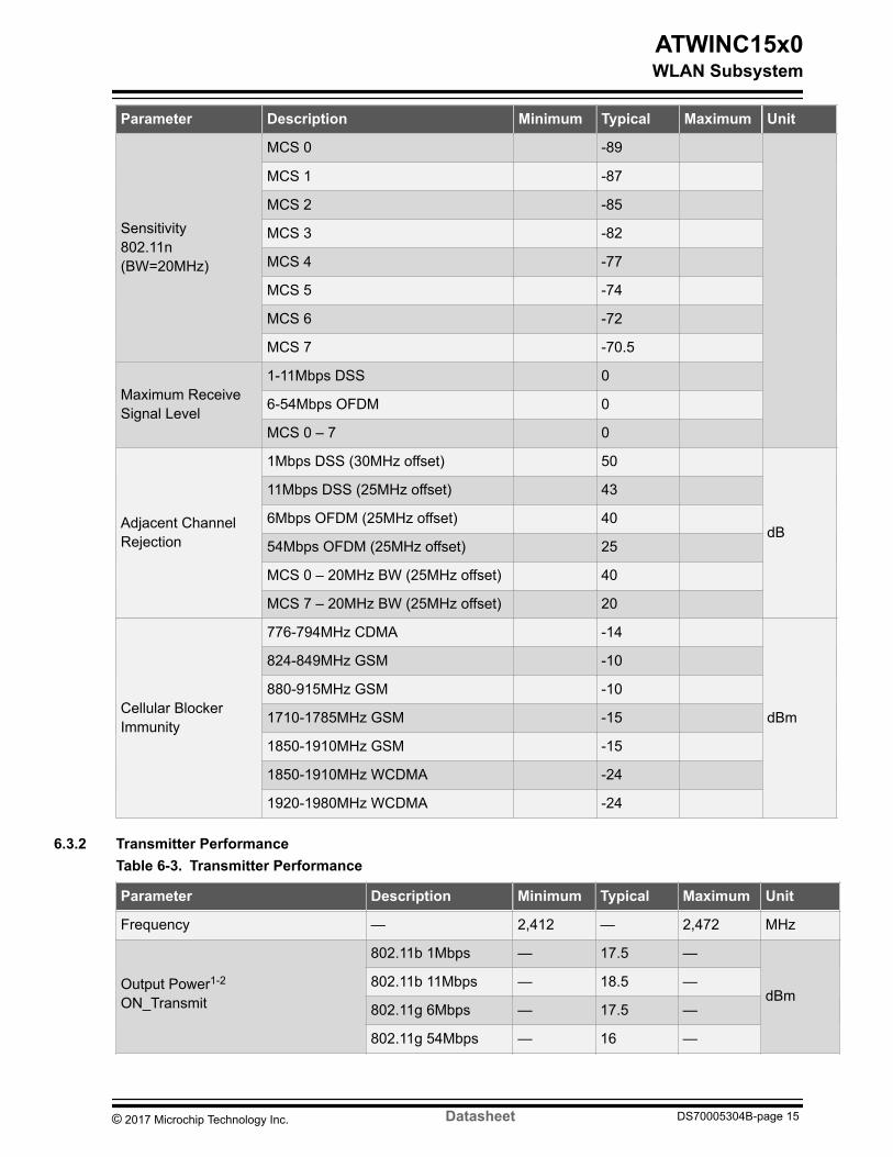
Parameter Description Minimum Typical Maximum Unit
80211n MCS 0 mdash 170 mdash
80211n MCS 7 mdash 145 mdash
TX Power Accuracy mdash mdash plusmn15 2 mdash dB
Carrier Suppression mdash mdash 300 mdash dBc
Harmonic Output Power2nd mdash -41
dBmMHz3rd mdash mdash -41
Note 1 Measured at 80211 spec compliant EVMSpectral Mask2 Measured after RF matching network3 Operating temperature range is -40degC to +85degC RF performance guaranteed at room temperature
of 25degC with a 2-3dB change at boundary conditions 4 With respect to TX power different (higherlower) RF output power settings may be used for
specific antennas andor enclosures in which case recertification may be required5 The availability of some specific channels andor operational frequency bands are country
dependent and should be programmed at the Host product factory to match the intendeddestination Regulatory bodies prohibit exposing the settings to the end user This requirementneeds to be taken care of via Host implementation
ATWINC15x0WLAN Subsystem
copy 2017 Microchip Technology Inc Datasheet DS70005304B-page 16
7 External Interfaces
71 Interfacing with the Host MicrocontrollerThis section describes interfacing the ATWINC15x0-MR210xB module with the host microcontroller Theinterface is comprised of a slave SPI and additional control signals as shown in the following figure Formore information on SPI interface specification and timing refer to the SPI Interface Additional controlsignals are connected to the GPIOIRQ interface of the microcontroller
Figure 7-1 Interfacing with Host Microcontroller
Host Microcontroller
CHIP_EN
RESET
WAKE
IRQN
SPI Wi-Fi Controller
Module
Table 7-1 Host Microcontroller Interface Pins
Pin Number Function
4 RESET_N
11 WAKE
13 IRQ_N
22 CHIP_EN
16 SPI_SSN
15 SPI_MOSI
17 SPI_MISO
18 SPI_SCK
Related LinksSPI Interface
ATWINC15x0External Interfaces
copy 2017 Microchip Technology Inc Datasheet DS70005304B-page 17
72 SPI Interface
721 OverviewThe ATWINC15x0-MR210xB has a Serial Peripheral Interface (SPI) that operates as an SPI slave TheSPI interface can be used for control and for serial IO of 80211 data The SPI pins are mapped asshown in the following table The SPI is a full-duplex slave-synchronous serial interface that is availableimmediately following reset when pin 10 (SPI_CFG) is tied to VDDIO
Table 7-2 SPI Interface Pin Mapping
Pin SPI function
10 CFG Must be tied to VDDIO
16 SSN Active-Low Slave Select
15 MOSI(RXD) Serial Data Receive
18 SCK Serial Clock
17 MISO(TXD) Serial Data Transmit
When the SPI is not selected that is when SSN is high the SPI interface will not interfere with datatransfers between the serial-master and other serial-slave devices When the serial slave is not selectedits transmitted data output is buffered resulting in a high impedance drive onto the MISO line
The SPI interface responds to a protocol that allows an external host to read or write any register in thechip as well as initiate DMA transfers
The SPI SSN MOSI MISO and SCK pins of the ATWINC15x0-MR210xB have internal programmablepull-up resistors These resistors should be programmed to be disabled otherwise if any of the SPI pinsare driven to a low level while the ATWINC15x0-MR210xB is in the low power sleep state the current willflow from the VDDIO supply through the pull-up resistors increasing the current consumption of themodule
Related LinksProgrammable Pull Up Resistors
722 SPI TimingThe SPI Slave interface supports four standard modes as determined by the Clock Polarity (CPOL) andClock Phase (CPHA) settings These modes are illustrated in the following table and figure
Table 7-3 SPI Slave Modes
Mode CPOL CPHA
0 0 0
1 0 1
2 1 0
3 1 1
The red lines in the following figure correspond to Clock Phase = 0 and the blue lines correspond to ClockPhase = 1
ATWINC15x0External Interfaces
copy 2017 Microchip Technology Inc Datasheet DS70005304B-page 18
Figure 7-2 SPI Slave Clock Polarity and Clock Phase Timing
z
z z
z
SCKCPOL = 0
CPOL = 1
SSN
RXDTXD(MOSIMISO)
CPHA = 0
CPHA = 1
2 3 4 5 6 7 8
1 2 3 4 5 6 7
1
8
The SPI timing is provided in the following figure and table
Figure 7-3 SPI Timing Diagram (SPI Mode CPOL=0 CPHA=0)
t LH
SCK
TXD
RXD
t WH
t HL
t WL
t ODLY
t ISU t IHD
f SCK
SSN
t SUSSN t HDSSN
Table 7-4 SPI Slave Timing Parameters1
Parameter Symbol Min Max Units
Clock Input Frequency2 fSCK mdash 48 MHz
Clock Low Pulse Width tWL 4 mdash
nsClock High Pulse Width tWH 5 mdash
Clock Rise Time tLH 0 7
Clock Fall Time tHL 0 7
ATWINC15x0External Interfaces
copy 2017 Microchip Technology Inc Datasheet DS70005304B-page 19
Parameter Symbol Min Max Units
TXD Output Delay3 tODLY 4 9 from SCK fall125 from SCKrise
RXD Input Setup Time tISU 1 mdash
RXD Input Hold Time tIHD 5 mdash
SSN Input Setup Time tSUSSN 3 mdash
SSN Input Hold Time tHDSSN 55 mdash
Note 1 Timing is applicable to all SPI modes2 Maximum clock frequency specified is limited by the SPI Slave interface internal design actual
maximum clock frequency can be lower and depends on the specific PCB layout3 Timing based on 15pF output loading
73 UART InterfaceThe ATWINC15x0-MR210xB supports the Universal Asynchronous ReceiverTransmitter (UART)interface This interface should be used for debug purposes only The UART is available on pins 14 and19 The UART is compatible with the RS-232 standard and the ATWINC15x0-MR210xB operates asData Terminal Equipment (DTE) It has a two-pin RXDTXD interface
The default configuration for accessing the UART interface of ATWINC15x0-MR210xB is mentionedbelow
bull Baud rate 115200bull Data 8 bitbull Parity Nonebull Stop bit 1 bitbull Flow control None
It also has RX and TX FIFOs which ensure reliable high-speed reception and low software overheadtransmission FIFO size is 4 x 8 for both RX and TX direction The UART also has status registersshowing the number of received characters available in the FIFO and various error conditions as well theability to generate interrupts based on these status bits
An example of the UART receiving or transmitting a single packet is shown in the following figure Thisexample shows 7-bit data (0x45) odd parity and two stop bits
Important UART2 supports RTS and CTS flow control The UART RTS and UART CTSMUST be connected to the host MCU UART and enabled for the UART interface to befunctional
ATWINC15x0External Interfaces
copy 2017 Microchip Technology Inc Datasheet DS70005304B-page 20
Figure 7-4 Example of UART RX of TX Packet
Previous Packets or
Leading Idle Bits
Current Packet
DataStart Bit
Parity Bit Stop Bits
Next Packet
ATWINC15x0External Interfaces
copy 2017 Microchip Technology Inc Datasheet DS70005304B-page 21
8 Power Consumption
81 Description of Device StatesThe ATWINC15x0-MR210xB has several device states
bull ON_Transmit ndash Device is actively transmitting an 80211 signal Highest output power and nominalcurrent consumption
bull ON_Receive ndash Device is actively receiving an 80211 signal Lowest sensitivity and nominal currentconsumption
bull ON_Doze ndash Device is ON but is neither transmitting nor receivingbull Power_Down ndash Device core supply off (Leakage)bull IDLE connect ndash Device is connected with 1 DTIM beacon interval
The following pins are used to switch between the ON and Power_Down states
bull CHIP_EN ndash Device pin (pin 22) used to enable DCDC Converterbull VDDIO ndash IO supply voltage from external supply
In the ON states VDDIO is on and CHIP_EN is high (at VDDIO voltage level) To switch betweenthe ON states and Power_Down state CHIP_EN has to change between high and low (GND)voltage When VDDIO is off and CHIP_EN is low the chip is powered off with no leakage (also see Restrictions for Power States)
82 Current Consumption in Various Device StatesTable 8-1 Current Consumption
Device State Code Rate Outputpower dBm
Current Consumption 1
IVBATT IVDDIO
ON_Transmit
80211b 1Mbps 175 268mA 22mA
80211b 11Mbps 185 264mA 22mA
80211g 6Mbps 175 269mA 22mA
80211g 54Mbps 160 266mA 22mA
80211n MCS 0 170 268mA 22mA
80211n MCS 7 145 265mA 22mA
ON_Receive
80211b 1Mbps NA 61mA 22mA
80211b 11Mbps NA 61mA 22mA
80211g 6Mbps NA 61mA 22mA
80211g 54Mbps NA 61mA 22mA
80211n MCS 0 NA 61mA 22mA
80211n MCS 7 NA 61mA 22mA
ATWINC15x0Power Consumption
copy 2017 Microchip Technology Inc Datasheet DS70005304B-page 22
Device State Code Rate Outputpower dBm
Current Consumption 1
IVBATT IVDDIO
ON_Doze NA NA 380microA lt10microA
Power_Down NA NA lt05microA lt35microA
Note
1 Measured conditions VBATT 33V VDDIO 33V temp 25degC
83 Restrictions for Power StatesWhen no power is supplied to the device for example the DCDC Converter output and VDDIO are bothoff (at ground potential) a voltage cannot be applied to the device pins because each pin contains anESD diode from the pin to supply This diode will turn on when a voltage higher than one diode drop issupplied to the pin
If a voltage must be applied to the signal pads while the chip is in a low-power state the VDDIO supplymust be on so the SLEEP or Power_Down state must be used
Similarly to prevent the pin-to-ground diode from turning on do not apply a voltage that is more than onediode drop below ground to any pin
84 Power-updown SequenceThe power-updown sequence for ATWINC15x0-MR210xB is shown in the Following Figure The timingparameters are provided in following the table
Figure 8-1 Power UpDown Sequence
VBATT
VDDIO
CHIP_EN
RESETN
t A
t B
t C
XO Clock
t B
t A
tC
Table 8-2 Power-updown Sequence Timing
Parameter Min Max Units Description Notes
tA0 ms VBATT rise to VDDIO
riseVBATT and VDDIO can risesimultaneously or can be tied
ATWINC15x0Power Consumption
copy 2017 Microchip Technology Inc Datasheet DS70005304B-page 23
Parameter Min Max Units Description Notes
together VDDIO must not risebefore VBATT
tB0 ms VDDIO rise to CHIP_EN
riseCHIP_EN must not rise beforeVDDIO CHIP_EN must be drivenhigh or low not left floating
tC
5 ms CHIP_EN rise toRESETN rise
This delay is needed because theXO clock must stabilize beforeRESETN removal RESETN mustbe driven high or low not leftfloating
tArsquo
0 ms VDDIO fall to VBATT fall VBATT and VDDIO can fallsimultaneously or can be tiedtogether VBATT must not fallbefore VDDIO
tBrsquo
0 ms CHIP_EN fall to VDDIOfall
VDDIO must not fall beforeCHIP_EN CHIP_EN and RESETNcan fall simultaneously
tCrsquo
0 ms RESETN fall to VDDIOfall
VDDIO must not fall beforeRESETN RESETN and CHIP_ENcan fall simultaneously
85 Digital IO Pin Behavior During Power-up SequencesThe following table represents digital IO Pin states corresponding to device power modes
Table 8-3 Digital IO Pin Behavior in Different Device States
Device state VDDIO CHIP_EN RESETN Outputdriver
Inputdriver
Pull updownresistor (96kΩ)
Power-Downcore supply off
High Low Low Disabled (Hi-Z) Disabled Disabled
Power-on Resetcore supply on hard reseton
High High Low Disabled (Hi-Z) Disabled Enabled
Power-On Defaultcore supply on the deviceis out of reset but notprogrammed yet
High High High Disabled (Hi-Z) Enabled Enabled
On SleepOn TransmitOn Receivecore supply on deviceprogrammed by firmware
High High High Programmed byfirmware foreach pinEnabled orDisabled
Oppositeof OutputDriverstate
Programmed byfirmware foreach pinEnabled orDisabled
ATWINC15x0Power Consumption
copy 2017 Microchip Technology Inc Datasheet DS70005304B-page 24
86 Module ResetIf a module reset is performed the RESETN pin must be pulsed low for a minimum of 1micro second
ATWINC15x0Power Consumption
copy 2017 Microchip Technology Inc Datasheet DS70005304B-page 25
9 Notes On Interfacing to the ATWINC15x0-MR210xB
91 Programmable Pull Up ResistorsThe ATWINC15x0-MR210xB provides programmable pull up resistors on various pins The purpose ofthese resistors is to keep any unused input pins from floating which can cause excess current to flowthrough the input buffer from the VDDIO supply Any unused module pin on the ATWINC15x0-MR210xBshould leave these pull up resistors enabled so the pin will not float The default state at power-up is forthe pull up resistor to be enabled However any pin that is used should have the pull up resistor disabledThe reason for this is that if any pins are driven to a low level while the ATWINC15x0-MR210xB is in thelow power sleep state current will flow from the VDDIO supply through the pull up resistors increasingthe current consumption of the module Since the value of the pull up resistor is approximately 100KΩthe current through any pull up resistor that is being driven low will be VDDIO100K For VDDIO = 33Vthe current through each pull up resistor that is driven low would be approximately 33V100K = 33microAPins which are used and have had the programmable pull up resistor disabled should always be activelydriven to either a high or low level and not be allowed to float
ATWINC15x0Notes On Interfacing to the ATWINC15x0-MR210xB
copy 2017 Microchip Technology Inc Datasheet DS70005304B-page 26
10 Schematic Design InformationThis section provides schematic information for reference Application schematics for SPI are provided inthe following figure Module design information such as module schematics can be obtained under anNDA from Microchip These schematics are applicable to the ATWINC1500-MR210PB ATWINC1510-MR210PB and the ATWINC1500-MR210UB modules
101 Application SchematicFigure 10-1 SPI Application Schematic
Resistors R2-R1 are recommendedAs placeholders in case filteringof noisy signals is required Theyalso allow disconnecting of module For debug purposes
Note Add 10uF and 001uF decoupling capacitors between the pin 24 (1P3V_TP) and GND
ATWINC15x0Schematic Design Information
copy 2017 Microchip Technology Inc Datasheet DS70005304B-page 27
11 Module DrawingThis section provides information about the module package outline drawings
Figure 11-1 Module Drawing - ATWINC15x0-MR210PB (unit = mm)
MODULE TOP VIEW
Metal Shield
Metal Shield
PCB
MODULE SIDE VIEW MODULE BOTTOM VIEW
NOTE THIS PAD MUST BE SOLDERED TO GND
NOT TO SCALE
ATWINC15x0Module Drawing
copy 2017 Microchip Technology Inc Datasheet DS70005304B-page 28
Figure 11-2 Module Drawings ndash ATWINC15x0-MR210UB (unit = mm)
MODULE TOP VIEW
Metal Shield
Metal Shield
PCB
MODULE SIDE VIEW MODULE BOTTOM VIEW
NOTE THIS PAD MUST BE SOLDERED TO GND
NOT TO SCALE Rev 2
111 Module FootprintThis section provides the outline drawing for the recommended footprint for the ATWINC15x0-MR210xBmodule It is imperative that the center Ground Pad is provided with an array of vias to provide for a goodground and thermal transfer for the ATWINC15x0-MR210xB module
This footprint is applicable to the ATWINC15x0-MR210xB module devices
ATWINC15x0Module Drawing
copy 2017 Microchip Technology Inc Datasheet DS70005304B-page 29
Figure 11-3 Module Solder Pad Footprint (unit = mm)
NOTE THIS PAD MUST BE TIED TO GND
1016 Pitch
1473
19
08
1016 Pitch
4064
267
267
600
1016 Pitch
370
370
1016 Pitch
19 3048
368
2172 2032
442
SOLDER PAD FOOTPRINT
Drawing not to scaleUntoleranced dimensionsUnits=mm
ATWINC15x0Module Drawing
copy 2017 Microchip Technology Inc Datasheet DS70005304B-page 30
12 Design ConsiderationsThis section provides the guidelines on placement and routing to achieve the best performance
121 ATWINC15x0-MR210PB Placement and Routing Guidelinesbull The module must be placed on the main board ndash the printed antenna area must overlap with the
carrier board The portion of the module containing the antenna should not go outside the edge ofthe main board The antenna is designed to work properly when it is sitting directly on top of a15mm thick printed circuit board
bull If the module is placed at the edge of the main board a minimum 22mm by 5mm area directlyunder the antenna must be clear of all metal on all layers of the board ldquoIn-landrdquo placement isacceptable however deepness of keep-out area must grove to module edge to main board edgeplus 5mm DO NOT PLACE THE MODULE IN THE MIDDLE OF THE MAIN BOARD OR FARAWAY FROM THE MAIN BOARD EDGE
bull Keep away from the antenna as far as possible large metal objects to avoid electromagnetic fieldblocking
bull Do not enclose the antenna within a metal shieldbull Keep any components which may radiate noise or signals within the 24GHz-25GHz frequency
band as far away from the antenna as possible or better yet shield those components Any noiseradiated from the main board in this frequency band will degrade the sensitivity of the module
Figure 12-1 ATWINC15x0-MR210PB Placement Reference
Best Case
Worst Case
System Ground Plane
(a)
(b)
Keep out area
Microchip
Microchip
122 Printed PCB Antenna Performance of ATWINC15x0-MR210PBThe printed PCB antenna on the ATWINC15x0-MR210PB is a meandered Inverted F Antenna (IFA) Theantenna is fed via matching network which is matched for the module installed on a 15mm thick main
ATWINC15x0Design Considerations
copy 2017 Microchip Technology Inc Datasheet DS70005304B-page 31
board Main board thickness deviation by plusmn1mm changes RXTX performance by plusmn1dB maximumreferring to RXTX performance with a default antenna matching network and installed on 15mm thickmain board
Measured peak antenna gain is -03dBi
Antenna Radiation PatternFollowing figures illustrate the Antenna Radiation PatternsFigure 12-2 Antenna Radiation Pattern when Phi = 0 degree
ATWINC15x0Design Considerations
copy 2017 Microchip Technology Inc Datasheet DS70005304B-page 32
Figure 12-3 Antenna Radiation Pattern when Phi = 90 degree
ATWINC15x0Design Considerations
copy 2017 Microchip Technology Inc Datasheet DS70005304B-page 33
Figure 12-4 Antenna Radiation Pattern when Theta = 90 degree
123 ATWINC15x0-MR210UB Placement and Routing GuidelinesThe ATWINC15x0-MR210UB module has an Ultra Small Miniature RF Connector (uFL) for the externalantenna
The choice of antenna is limited to the antenna types for which the module was tested and approved Fora list of tested and approved antennas that may be used with the module refer to the respective countryin Regulatory Approval
An approved and tested antenna type is shown in the following table
Table 12-1 Tested External Antenna Type
Antenna Type Gain
Whip Antenna 22dBi
ATWINC15x0Design Considerations
copy 2017 Microchip Technology Inc Datasheet DS70005304B-page 34
1231 Recommended External Antenna for ATWINC15x0-MR210UBWhip Antenna (Part number RN-SMA-4) along with a 10cm length RF cable assembly (uFL to SMA) hasbeen used for the certification of ATWINC15x0-MR210UB It is recommended to use the same or similarexternal antenna in design
124 Module Assembly ConsiderationsThe ATWINC15x0-MR210xB modules are assembled with an EMI Shield to ensure compliance with EMIemission and immunity rules The EMI shield is made of a tin-plated steel (SPTE) and is not hermeticallysealed Solutions like IPA and similar solvents can be used to clean the ATWINC15x0-MR210xB moduleHowever cleaning solutions that contain acid should never be used on the module
The ATWINC15x0-MR210xB modules are manufactured without any conformal coating applied It is thecustomerrsquos responsibility if a conformal coating is specified andor applied to the ATWINC15x0-MR210xBmodule
ATWINC15x0Design Considerations
copy 2017 Microchip Technology Inc Datasheet DS70005304B-page 35
13 Reflow Profile InformationThis chapter provides guidelines for reflow processes in getting the Microchip module soldered to thecustomerrsquos design
131 Storage Condition
1311 Moisture Barrier Bag Before OpeningA moisture barrier bag must be stored in a temperature of less than 30degC with humidity under 85 RH
The calculated shelf life for the dry-packed product shall be 12 months from the date the bag is sealed
1312 Moisture Barrier Bag OpenHumidity indicator cards must be blue lt30
132 Solder PasteSn-Ag-Cu eutectic solder with melting temperature of 217degC is most commonly used for lead-free solderreflow application This alloy is widely accepted in the semiconductor industry due to its low costrelatively low melting temperature and good thermal fatigue resistance Some recommended pastesinclude NC-SMQreg 230 flux and Indalloyreg 241 solder paste made up of 955 Sn38 Ag07 Cu or SENJUN705-GRN3360-K2-V Type 3 no clean paste
133 Stencil DesignThe recommended stencil is laser-cut stainless steel type with a thickness of 100microm to 130microm andapproximately a 11 ratio of stencil opening to pad dimension To improve paste release a positive taperwith bottom opening 25microm larger than the top can be utilized Local manufacturing experience may findother combinations of stencil thickness and aperture size to get good results
134 Printing ProcessThe printing process requires no significant changes compared to SnPb solder Any guidelinesrecommended by the paste manufacturers to accommodate paste specific characteristics should befollowed Post-print inspection and paste volume measurement is very critical to ensure good print qualityand uniform paste
135 Baking ConditionsThis module is rated at MSL level 3 After a sealed bag is opened no baking is required within 168 hoursso long as the devices are held at le30degC60 RH or stored at lt10 RH
The module will require baking before mounting if
bull The sealed bag has been open for gt168 hoursbull Humidity Indicator Card reads gt10bull SIPs need to be baked for 8 hours at 125degC
ATWINC15x0Reflow Profile Information
copy 2017 Microchip Technology Inc Datasheet DS70005304B-page 36
136 Soldering and Reflow ConditionThe optimization of the reflow process is the most critical factor to be considered for lead-free solderingThe development of an optimal profile should take into account the paste characteristics the size of theboard the density of the components the mix of the larger and smaller components and the peaktemperature requirements of the components An optimized reflow process is the key to ensuring asuccessful lead-free assembly and achieves high yield and long term solder joint reliability
Temperature ProfilingTemperature profiling should be performed for all new board designs by attaching thermocouples at thesolder joints on the top surface of the larger components and at multiple locations of the boards This isto ensure that all components are heated to a temperature above the minimum reflow temperatures andthe smaller components do not exceed maximum temperature limit The SnAgCu solder alloy melts at~217degC so the reflow temperature peak at joint level should be 15 to 20degC higher than meltingtemperature The targeted solder joint temperature for the Sn-Ag-Cu solder should be ~235degC For largeror sophisticated boards with a large mix of components it is also important to ensure that thetemperature difference across the board is less than 10 degrees to minimize board warpage Themaximum temperature at the component body should not exceed the MSL3 qualification specification
1361 Reflow OvenIt is strongly recommended that a reflow oven equipped with more heating zones and Nitrogenatmosphere should be used for lead-free assembly Nitrogen atmosphere has shown to improve the wet-ability and reduce temperature gradient across the board It can also enhance the appearance of thesolder joints by reducing the effects of oxidation
The following items should also be observed in the reflow process
1 Some recommended pastes includendash NC-SMQreg 230 flux and Indalloyreg 241 solder paste made up of 955 Sn38 Ag07 Cundash SENJU N705-GRN3360-K2-V Type 3 no clean paste
2 Allowable reflow soldering iterationsndash Three times based on the following reflow soldering profile (refer following Figure)
3 Temperature profilendash Reflow soldering shall be done according to the following temperature profile (refer to the
following figure)ndash Peak temperature 250degC
ATWINC15x0Reflow Profile Information
copy 2017 Microchip Technology Inc Datasheet DS70005304B-page 37
Figure 13-1 Solder Reflow Profile
25oC
Slope 1~2oCsec max(217oC to peak)
(Peak 250oC)
Ramp down rate Max 25oCsec
Time (sec)
40 ~ 70 sec60 ~ 120 sec
Ramp up rate Max 25oCsec
Preheat150 ~ 200oC
217oC
CleaningThe exposed ground paddle helps to self-align the module avoiding pad misalignment The use of noclean solder pastes is recommended Full drying of no-clean paste fluxes as a result of the reflow processmust be ensured This may require longer reflow profiles andor peak temperatures toward the high endof the process window as recommended by the solder paste vendor It is believed that uncured fluxresidues could lead to corrosion andor shorting in accelerated testing and possibly the field
ReworkRework is to remove the mounted SIP package and replace with a new unit It is recommended that oncean ATWINC15x0-MR210xB Module has been removed it should never be reused During the reworkprocess the mounted module and PCB are heated partially and the module is removed It isrecommended to pay attention to heat-proof the proximity of the mounted parts and junctions and use thebest nozzle for rework that is suited to the module size
ATWINC15x0Reflow Profile Information
copy 2017 Microchip Technology Inc Datasheet DS70005304B-page 38
14 Regulatory ApprovalRegulatory Approvals received
ATWINC1500-MR210PBbull United StatesFCC ID 2ADHKATWINC1500bull Canada
ndash IC 20266-WINC1500PBndash HVIN ATWINC1500-MR210PB
bull Europe - CE
ATWINC1510-MR210PBbull United StatesFCC ID 2ADHKATWINC1510bull Canada
ndash IC 20266-ATWINC1510ndash HVIN ATWINC1510-MR210PB
bull Europe - CE
ATWINC1500-MR210UBbull United StatesFCC ID 2ADHKATWINC1500Ubull Canada
ndash IC 20266-WINC1500UBndash HVIN ATWINC1500-MR210UB
141 United StatesThe ATWINC1500-MR210PB ATWINC1510-MR210PB and ATWINC1500-MR210UB modules havereceived Federal Communications Commission (FCC) CFR47 Telecommunications Part 15 Subpart CldquoIntentional Radiatorsrdquo single-modular approval in accordance with Part 15212 Modular Transmitterapproval Single-modular transmitter approval is defined as a complete RF transmission sub-assemblydesigned to be incorporated into another device that must demonstrate compliance with FCC rules andpolicies independent of any host A transmitter with a modular grant can be installed in different end-useproducts (referred to as a host host product or host device) by the grantee or other equipmentmanufacturer then the host product may not require additional testing or equipment authorization for thetransmitter function provided by that specific module or limited module device
The user must comply with all of the instructions provided by the Grantee which indicate installationandor operating conditions necessary for compliance
A host product itself is required to comply with all other applicable FCC equipment authorizationregulations requirements and equipment functions that are not associated with the transmitter moduleportion For example compliance must be demonstrated to regulations for other transmitter componentswithin a host product to requirements for unintentional radiators (Part 15 Subpart B) such as digitaldevices computer peripherals radio receivers etc and to additional authorization requirements for thenon-transmitter functions on the transmitter module (ie Verification or Declaration of Conformity) asappropriate (eg Bluetooth and Wi-Fi transmitter modules may also contain digital logic functions)
1411 Labeling And User Information RequirementsThe ATWINC1500-MR210PB ATWINC1510-MR210PB and ATWINC1500-MR210UB modules havebeen labeled with its own FCC ID number and if the FCC ID is not visible when the module is installed
ATWINC15x0Regulatory Approval
copy 2017 Microchip Technology Inc Datasheet DS70005304B-page 39
inside another device then the outside of the finished product into which the module is installed mustdisplay a label referring to the enclosed module This exterior label should use the following wording
For the ATWINC1500-MR210PB
Contains Transmitter Module FCC ID 2ADHKATWINC1500
or
Contains FCC ID 2ADHKATWINC1500
This device complies with Part 15 of the FCC Rules Operation is subject to the following twoconditions (1) this device may not cause harmful interference and (2) this device must acceptany interference received including interference that may cause undesired operation
For the ATWINC1510-MR210PB
Contains Transmitter Module FCC ID 2ADHKATWINC1510
or
Contains FCC ID 2ADHKATWINC1510
This device complies with Part 15 of the FCC Rules Operation is subject to the following twoconditions (1) this device may not cause harmful interference and (2) this device must acceptany interference received including interference that may cause undesired operation
For the ATWINC1500-MR210UB
Contains Transmitter Module FCC ID 2ADHKATWINC1500U
or
Contains FCC ID 2ADHKATWINC1500U
This device complies with Part 15 of the FCC Rules Operation is subject to the following twoconditions (1) this device may not cause harmful interference and (2) this device must acceptany interference received including interference that may cause undesired operation
The users manual for the finished product should include the following statement
This equipment has been tested and found to comply with the limits for a Class B digital devicepursuant to part 15 of the FCC Rules These limits are designed to provide reasonable protectionagainst harmful interference in a residential installation This equipment generates uses and can radiateradio frequency energy and if not installed and used in accordance with the instructions may causeharmful interference to radio communications However there is no guarantee that interference will notoccur in a particular installation If this equipment does cause harmful interference to radio or televisionreception which can be determined by turning the equipment off and on the user is encouraged to tryto correct the interference by one or more of the following measures
bull Reorient or relocate the receiving antennabull Increase the separation between the equipment and receiverbull Connect the equipment into an outlet on a circuit different from that to which the receiver is
connectedbull Consult the dealer or an experienced radioTV technician for help
ATWINC15x0Regulatory Approval
copy 2017 Microchip Technology Inc Datasheet DS70005304B-page 40
Additional information on labeling and user information requirements for Part 15 devices can be found inKDB Publication 784748 which is available at the FCC Office of Engineering and Technology (OET)Laboratory Division Knowledge Database (KDB) httpsappsfccgovoetcfkdbindexcfm
1412 RF ExposureAll transmitters regulated by FCC must comply with RF exposure requirements KDB 447498 General RFExposure Guidance provides guidance in determining whether proposed or existing transmitting facilitiesoperations or devices comply with limits for human exposure to Radio Frequency (RF) fields adopted bythe Federal Communications Commission (FCC)
From the FCC Grant Output power listed is conducted This transmitter is restricted for use with thespecific antenna(s) tested in this application for Certification
In the end product the antenna(s) used with this transmitter must be installed to provide a separationdistance of at least 65 cm from all persons and must not be co-located or operation in conjunction withany other antenna or transmitter User and installers must be provided with antenna installationinstructions and transmitter operating conditions for satisfying the RF exposure compliance
1413 Approved Antenna TypesTo maintain modular approval in the United States only the antenna types that have been tested shall beused It is permissible to use different antenna provided the same antenna type and antenna gain (equalto or less than) is used An antenna type comprises antennas having similar in-band and out-of-bandradiation patterns
Testing the ATWINC1500-MR210UB module was performed with the antenna types listed in Table 12-1
1414 Helpful Web SitesFederal Communications Commission (FCC) httpwwwfccgov
FCC Office of Engineering and Technology (OET) Laboratory Division Knowledge Database (KDB)
httpsappsfccgovoetcfkdbindexcfm
142 CanadaThe ATWINC1500-MR210PB ATWINC1510-MR210PB and ATWINC1500-MR210UB modules havebeen certified for use in Canada under Innovation Science and Economic Development Canada (ISEDformerly Industry Canada) Radio Standards Procedure (RSP) RSP-100 Radio Standards Specification(RSS) RSS-Gen and RSS-247 Modular approval permits the installation of a module in a host devicewithout the need to recertify the device
1421 Labeling and User Information RequirementsLabeling Requirements (from RSP-100 - Issue 11 Section 3) The host product shall be properly labeledto identify the module within the host device
The Innovation Science and Economic Development Canada certification label of a module shall beclearly visible at all times when installed in the host device otherwise the host product must be labeled todisplay the Innovation Science and Economic Development Canada certification number of the modulepreceded by the word ldquoContainsrdquo or similar wording expressing the same meaning as follows
For the ATWINC1500-MR210PB
Contains IC 20266-WINC1500PB
ATWINC15x0Regulatory Approval
copy 2017 Microchip Technology Inc Datasheet DS70005304B-page 41
For the ATWINC1510-MR210PB
Contains IC 20266-ATWINC1510
For the ATWINC1500-MR210UB module
Contains IC 20266-WINC1500UB
User Manual Notice for License-Exempt Radio Apparatus (from Section 84 RSS-Gen Issue 4November 2014) User manuals for license-exempt radio apparatus shall contain the following orequivalent notice in a conspicuous location in the user manual or alternatively on the device or both
This device complies with Industry Canadas license exempt RSS standard(s) Operation issubject to the following two conditions
(1) This device may not cause interference and
(2) This device must accept any interference including interference that may cause undesiredoperation of the device
Le preacutesent appareil est conforme aux CNR dIndustrie Canada applicables aux appareils radioexempts de licence Lexploitation est autoriseacutee aux deux conditions suivantes
(1) lappareil ne doit pas produire de brouillage et
(2) lutilisateur de lappareil doit accepter tout brouillage radioeacutelectrique subi mecircme si lebrouillage est susceptible den compromettre le fonctionnement
Guidelines on Transmitter Antenna for License Exempt Radio Apparatus
Under Industry Canada regulations this radio transmitter may only operate using an antenna ofa type and maximum (or lesser) gain approved for the transmitter by Industry Canada To reducepotential radio interference to other users the antenna type and its gain should be so chosenthat the equivalent isotropically radiated power (eirp) is not more than that necessary forsuccessful communication
Conformeacutement agrave la reacuteglementation dIndustrie Canada le preacutesent eacutemetteur radio peutfonctionner avec une antenne dun type et dun gain maximal (ou infeacuterieur) approuveacute pourleacutemetteur par Industrie Canada Dans le but de reacuteduire les risques de brouillage radioeacutelectriqueagrave lintention des autres utilisateurs il faut choisir le type dantenne et son gain de sorte que lapuissance isotrope rayonneacutee eacutequivalente (pire) ne deacutepasse pas lintensiteacute neacutecessaire agraveleacutetablisse-ment dune communication satisfaisante
Immediately following the above notice the manufacturer shall provide a list of all antenna typesapproved for use with the transmitter indicating the maximum permissible antenna gain (in dBi) andrequired impedance for each
1422 Transmitter Antenna (From Section 83 RSS-GEN Issue 4 November 2014)User manuals for transmitters equipped with detachable antennas shall also contain the following noticein a conspicuous location
This radio transmitter (identify the device by certification number or model number if CategoryII) has been approved by Industry Canada to operate with the antenna types listed below with themaximum permissible gain and required antenna impedance for each antenna type indicated
ATWINC15x0Regulatory Approval
copy 2017 Microchip Technology Inc Datasheet DS70005304B-page 42
Antenna types not included in this list having a gain greater than the maximum gain indicatedfor that type are strictly prohibited for use with this device
Le preacutesent eacutemetteur radio (identifier le dispositif par son numeacutero de certification) a eacuteteacute approuveacutepar Industrie Canada pour fonctionner avec les types dantenne eacutenumeacutereacutes ci‑dessous et ayantun gain admissible maximal Les types dantenne non inclus dans cette liste et dont le gain estsupeacuterieur au gain maximal indiqueacute sont strictement interdits pour lexploitation de leacutemetteur
1423 RF ExposureAll transmitters regulated by Innovation Science and Economic Development Canada (ISED) mustcomply with RF exposure requirements listed in RSS-102 - Radio Frequency (RF) Exposure Complianceof Radiocommunication Apparatus (All Frequency Bands)
This transmitter is restricted for use with a specific antenna tested in this application for certification andmust not be co-located or operating in conjunction with any other antenna or transmitters within a hostdevice except in accordance with Canada multi-transmitter product procedures
The installation of the transmitter must ensure that the antenna has a separation distance of at least 65cm from all persons or compliance must be demonstrated according to the ISED SAR procedures
1424 Helpful Web SitesInnovation Science and Economic Development Canada (ISED) httpwwwicgcca
143 EuropeThe ATWINC15x0-MR210PB module is a Radio Equipment Directive (RED) assessed radio module thatis CE marked and has been manufactured and tested with the intention of being integrated into a finalproduct
The ATWINC15x0-MR210PB module has been tested to RED 201453EU Essential Requirements forHealth and Safety (Article (31(a)) Electromagnetic Compatibility (EMC) (Article 31(b)) and Radio(Article 32) which is summarized in the following European Compliance Testing table
The ETSI provides guidance on modular devices in the ldquoGuide to the application of harmonised standardscovering articles 31b and 32 of the RED 201453EU (RED) to multi-radio and combined radio and non-radio equipmentrdquo document available at httpwwwetsiorgdeliveretsi_eg203300_203399203367010101_60eg_203367v010101ppdf
Note To maintain conformance to the testing listed in the following European Compliance Testing tablethe module shall be installed in accordance with the installation instructions in this data sheet and shallnot be modified When integrating a radio module into a completed product the integrator becomes themanufacturer of the final product and is therefore responsible for demonstrating compliance of the finalproduct with the essential requirements against the RED
1431 Labeling and User Information RequirementsThe label on the final product that contains the ATWINC15x0-MR210PB module must follow CE markingrequirements
ATWINC15x0Regulatory Approval
copy 2017 Microchip Technology Inc Datasheet DS70005304B-page 43
Table 14-1 European Compliance Testing (ATWINC15x0-MR210PB)
Certification Standards Article Laboratory ReportNumber
Date
Safety EN60950-12006A112009A12010 A122011A22013
[31(a)]
TUVRheinland
Taiwan
10059657001 2017-02-20
Health EN300328 V191EN623112008
50068130002
2017-02-20
EMC
EN301489-1 V192
[31(b)]
10058459002 2017-02-20
EN301489-17 V221
EN301489-1 V211EN301489-1 V220 10058459
003 2017-05-25EN301489-17 V311EN301489-17 V320
Radio EN300328 V191
(32)
50068130002
2017-02-20
EN300328 V211 50068130003 2017-05-26
1432 Conformity AssessmentFrom ETSI Guidance Note EG 203367 section 61 when non-radio products are combined with a radioproduct
If the manufacturer of the combined equipment installs the radio product in a host non-radio product inequivalent assessment conditions (ie host equivalent to the one used for the assessment of the radioproduct) and according to the installation instructions for the radio product then no additional assessmentof the combined equipment against article 32 of the RED is required
The European Compliance Testing listed in the preceeding table was performed using the integral chipantenna
14321 Simplified EU Declaration of ConformityHereby Microchip Technology Inc declares that the radio equipment type ATWINC15x0-MR210PB is incompliance with Directive 201453EU
The full text of the EU declaration of conformity for this product is available at httpwwwmicrochipcomdesign-centerswireless-connectivity
1433 Helpful WebsitesA document that can be used as a starting point in understanding the use of Short Range Devices (SRD)in Europe is the European Radio Communications Committee (ERC) Recommendation 70-03 E whichcan be downloaded from the European Communications Committee (ECC) at httpwwwecodocdbdk
Additional helpful web sites are
bull Radio Equipment Directive (201453EU)httpseceuropaeugrowthsingle-marketeuropean-standardsharmonised-standardsred_en
bull European Conference of Postal and Telecommunications Administrations (CEPT)httpwwwceptorg
ATWINC15x0Regulatory Approval
copy 2017 Microchip Technology Inc Datasheet DS70005304B-page 44
bull European Telecommunications Standards Institute (ETSI)httpwwwetsiorg
bull The Radio Equipment Directive Compliance Association (REDCA)httpwwwredcaeu
144 Other Regulatory Informationbull For information about other countries jurisdictions not covered here refer to http
wwwmicrochipcomdesign-centerswireless-connectivitybull Should other regulatory jurisdiction certification be required by the customer or the customer needs
to recertify the module for other reasons contact Microchip for the required utilities anddocumentation
ATWINC15x0Regulatory Approval
copy 2017 Microchip Technology Inc Datasheet DS70005304B-page 45
15 Reference Documentation and Support
151 Reference DocumentsThe following table provides the set of collateral documents to ease integration and device ramp
Table 15-1 Reference Documents
Title Content
ATWINC1500 MU DeviceDatasheet
Datasheet for the ATWINC1500 SmartConnect Wi-Fi componentFor more details contact a Microchip sales representative
Platform Getting Started Guide Details on how to evaluate the WINC15X0 Network ControllerModule
Flash Memory DownloadProcedure
Details the download procedures of firmware root certificate gaintable values etc
ATWINC1500 Wi-Fi NetworkController Software Design Guide
Integration guide with a clear description of High-level Arch anoverview on how to write a networking application list all APIsparameters and structuresFeatures of the device SPIhandshake protocol between deviceand host MCU with flowsequencestate diagram and timing
Software Programming Guide(ATWINC15x0)
Details the flow chart and how to use each API to implement allgeneric use cases (for example start AP start STA provisioningUDP TCP HTTP TLS p2p errors management connectiontransfer recovery mechanismstate diagram) - usage and sampleapplication note
Note A Design Files Package is available under NDA For more details contact a Microchip salesrepresentative
For a complete listing of development-support tools and documentation visit wwwmicrochipcom or referto the customer support section on options to locate the nearest Microchip field representative
ATWINC15x0Reference Documentation and Support
copy 2017 Microchip Technology Inc Datasheet DS70005304B-page 46
16 Document Revision HistoryNote The datasheet revision is independent of the die revision (Revision bit in the Device Identificationregister of the Device Service Unit DSUDIDREVISION) and the device variant (last letter of the orderingnumber)
Rev B - 122017
Section Changes
Introduction Editorial updates
Features Editorial updates
Regulatory Approvals Revised the content of certifications
Reference Documents Updated Table 15-1
Rev A - 022017
Section Changes
Document bull Change of document stylebull Change the name to incorporate all the
ATWINC15x0-MR210xB module familybull New Microchip document number Previous
version was Atmel document 42502 rev B
Product Description bull Added description information indicating thatthe document content is relevant to allWINC1500 Module models unless noted
bull Changed SSL references to TLSbull Removed WAPI securitybull Removed UART as host interfacebull Editorial updates
Product Features bull Removed WAPI securitybull Removed UART and I2C as host interfacesbull Removed Bluetooth coexistance interfacebull Replaced SSL with TLSbull Added 26 MHz crystalbull Removed (4KB flash ndash less than 1KB RAM)
Order Information and Module Marking bull Revised Ordering tablebull Revised Marking information Figure
Block Diagram bull Revised Block Diagram figure
Pin Description bull Revised Pin Description drawingbull Editorial updates
ATWINC15x0Document Revision History
copy 2017 Microchip Technology Inc Datasheet DS70005304B-page 47
Section Changes
Electrical Specifications bull Revised VDDIO maximum voltage in table41 and added max temperatures
bull Revised table 4-2 to include Recommendedoperating temperature
CPU and Memory Subsystems bull Editorial update
WLAN Subsystem RADIO bull Added text regarding performance deratingat cold temperature
bull Features table revisions and changesndash Corrected the package heightndash Revised Storage temperature
bull Added performance test conditions to theperformance tables
bull Revised the Receive performance in table6-2
bull Revised the 80211b mode Transmitperformance numbers in table 6-3
bull Revised Transmit performance Footnotesbull Changed max frequency to 2472GHzbull Editorial updates
External Interfaces bull Revised SPI timing information in table 7-3bull Removed Bluetooth Coexistance sectionbull Removed SDIObull Editorial updates
Power Consumption bull Added Module Reset section for resetduration
bull Editorial updates
ATWINC15x0-MR210PB Placement and RoutingGuidelines
bull Added text for antenna types used in testand an associated table
bull Revised Co-Ax connector type
Schematic Design Information bull Removed SDIO schematicbull Editorial updates
Module Drawings bull Updated module drawing figures and figuretitles
bull Added section with footprint drawing
Design Considerations bull Added sections for Module design andassembly considerations and module PCBplacement
Reflow Profile Information bull Revised reflow profile picture to be clearer
ATWINC15x0Document Revision History
copy 2017 Microchip Technology Inc Datasheet DS70005304B-page 48
Section Changes
bull Editorial updates
Certification Notices bull Added section for Agency Certificationnotices (now under Regulatory Approvalswith Rev B)
Agency Regulatory Approvals bull Added back Agency Approval sectionbull Revised content of certifications
Reference Documents bull Moved Design File Package to a separateparagraph below the table to remove webavailability aspect and to contact sales
Rev B - 022016
Document bull Updated copyright date to 2016bull Updated footers
Module Outline Drawing bull Revised Module outline drawings to showGround pad to be soldered
bull Pulled out Footprint drawing as this iscovered in the Module drawing
WLAN Subsystem Radio bull Revised Transmit Performance Table 6-3
Power Consumption bull Revised current table references in Table8-1
Schematic Design Information bull Updated Schematics Section 11 text andfigures Figure 11-1 and Figure 11-2
Reflow Profile Information bull Revised section 12 Reflow ProfileInformation
Reference Documents bull Updated Document Reference table toinclude the ATWINC1500-MU datasheet
Rev A - 072015
Document Updated due to changes in the ATWINC1500 fromRev A to Rev B
Description bull Updated model revisions to rev Bbull Corrected Package dimensions
Features bull Added Hardware Accelerator content tofeatures list
Pinout Information bull Updated reference schematic
ATWINC15x0Document Revision History
copy 2017 Microchip Technology Inc Datasheet DS70005304B-page 49
bull New pin list adds GPIOs 345 and 6
CPU and Memory Subsystems bull Increased Memory from 182KB to 160KB
External Interfaces bull Improved and corrected description ofCoexistence interface
bull Editorial updates
Power Consumption bull Updated power numbers and descriptionadded high-power and low-power modes
WLAN Subsystem Radio bull Updated Performance numbers
ATWINC15x0Document Revision History
copy 2017 Microchip Technology Inc Datasheet DS70005304B-page 50
The Microchip Web Site
Microchip provides online support via our web site at httpwwwmicrochipcom This web site is used asa means to make files and information easily available to customers Accessible by using your favoriteInternet browser the web site contains the following information
bull Product Support ndash Data sheets and errata application notes and sample programs designresources userrsquos guides and hardware support documents latest software releases and archivedsoftware
bull General Technical Support ndash Frequently Asked Questions (FAQ) technical support requestsonline discussion groups Microchip consultant program member listing
bull Business of Microchip ndash Product selector and ordering guides latest Microchip press releaseslisting of seminars and events listings of Microchip sales offices distributors and factoryrepresentatives
Customer Change Notification Service
Microchiprsquos customer notification service helps keep customers current on Microchip productsSubscribers will receive e-mail notification whenever there are changes updates revisions or erratarelated to a specified product family or development tool of interest
To register access the Microchip web site at httpwwwmicrochipcom Under ldquoSupportrdquo click onldquoCustomer Change Notificationrdquo and follow the registration instructions
Customer Support
Users of Microchip products can receive assistance through several channels
bull Distributor or Representativebull Local Sales Officebull Field Application Engineer (FAE)bull Technical Support
Customers should contact their distributor representative or Field Application Engineer (FAE) for supportLocal sales offices are also available to help customers A listing of sales offices and locations is includedin the back of this document
Technical support is available through the web site at httpwwwmicrochipcomsupport
Microchip Devices Code Protection Feature
Note the following details of the code protection feature on Microchip devices
bull Microchip products meet the specification contained in their particular Microchip Data Sheetbull Microchip believes that its family of products is one of the most secure families of its kind on the
market today when used in the intended manner and under normal conditionsbull There are dishonest and possibly illegal methods used to breach the code protection feature All of
these methods to our knowledge require using the Microchip products in a manner outside theoperating specifications contained in Microchiprsquos Data Sheets Most likely the person doing so isengaged in theft of intellectual property
bull Microchip is willing to work with the customer who is concerned about the integrity of their code
ATWINC15x0
copy 2017 Microchip Technology Inc Datasheet DS70005304B-page 51
bull Neither Microchip nor any other semiconductor manufacturer can guarantee the security of theircode Code protection does not mean that we are guaranteeing the product as ldquounbreakablerdquo
Code protection is constantly evolving We at Microchip are committed to continuously improving thecode protection features of our products Attempts to break Microchiprsquos code protection feature may be aviolation of the Digital Millennium Copyright Act If such acts allow unauthorized access to your softwareor other copyrighted work you may have a right to sue for relief under that Act
Legal Notice
Information contained in this publication regarding device applications and the like is provided only foryour convenience and may be superseded by updates It is your responsibility to ensure that yourapplication meets with your specifications MICROCHIP MAKES NO REPRESENTATIONS ORWARRANTIES OF ANY KIND WHETHER EXPRESS OR IMPLIED WRITTEN OR ORAL STATUTORYOR OTHERWISE RELATED TO THE INFORMATION INCLUDING BUT NOT LIMITED TO ITSCONDITION QUALITY PERFORMANCE MERCHANTABILITY OR FITNESS FOR PURPOSEMicrochip disclaims all liability arising from this information and its use Use of Microchip devices in lifesupport andor safety applications is entirely at the buyerrsquos risk and the buyer agrees to defendindemnify and hold harmless Microchip from any and all damages claims suits or expenses resultingfrom such use No licenses are conveyed implicitly or otherwise under any Microchip intellectualproperty rights unless otherwise stated
Trademarks
The Microchip name and logo the Microchip logo AnyRate AVR AVR logo AVR Freaks BeaconThingsBitCloud CryptoMemory CryptoRF dsPIC FlashFlex flexPWR Heldo JukeBlox KeeLoq KeeLoq logoKleer LANCheck LINK MD maXStylus maXTouch MediaLB megaAVR MOST MOST logo MPLABOptoLyzer PIC picoPower PICSTART PIC32 logo Prochip Designer QTouch RightTouch SAM-BASpyNIC SST SST Logo SuperFlash tinyAVR UNIO and XMEGA are registered trademarks ofMicrochip Technology Incorporated in the USA and other countries
ClockWorks The Embedded Control Solutions Company EtherSynch Hyper Speed Control HyperLightLoad IntelliMOS mTouch Precision Edge and Quiet-Wire are registered trademarks of MicrochipTechnology Incorporated in the USA
Adjacent Key Suppression AKS Analog-for-the-Digital Age Any Capacitor AnyIn AnyOut BodyComchipKIT chipKIT logo CodeGuard CryptoAuthentication CryptoCompanion CryptoControllerdsPICDEM dsPICDEMnet Dynamic Average Matching DAM ECAN EtherGREEN In-Circuit SerialProgramming ICSP Inter-Chip Connectivity JitterBlocker KleerNet KleerNet logo Mindi MiWimotorBench MPASM MPF MPLAB Certified logo MPLIB MPLINK MultiTRAK NetDetach OmniscientCode Generation PICDEM PICDEMnet PICkit PICtail PureSilicon QMatrix RightTouch logo REALICE Ripple Blocker SAM-ICE Serial Quad IO SMART-IS SQI SuperSwitcher SuperSwitcher II TotalEndurance TSHARC USBCheck VariSense ViewSpan WiperLock Wireless DNA and ZENA aretrademarks of Microchip Technology Incorporated in the USA and other countries
SQTP is a service mark of Microchip Technology Incorporated in the USA
Silicon Storage Technology is a registered trademark of Microchip Technology Inc in other countries
GestIC is a registered trademark of Microchip Technology Germany II GmbH amp Co KG a subsidiary ofMicrochip Technology Inc in other countries
All other trademarks mentioned herein are property of their respective companies
ATWINC15x0
copy 2017 Microchip Technology Inc Datasheet DS70005304B-page 52
copy 2017 Microchip Technology Incorporated Printed in the USA All Rights Reserved
ISBN 978-1-5224-2512-0
Quality Management System Certified by DNV
ISOTS 16949Microchip received ISOTS-169492009 certification for its worldwide headquarters design and waferfabrication facilities in Chandler and Tempe Arizona Gresham Oregon and design centers in Californiaand India The Companyrsquos quality system processes and procedures are for its PICreg MCUs and dsPICreg
DSCs KEELOQreg code hopping devices Serial EEPROMs microperipherals nonvolatile memory andanalog products In addition Microchiprsquos quality system for the design and manufacture of developmentsystems is ISO 90012000 certified
ATWINC15x0
copy 2017 Microchip Technology Inc Datasheet DS70005304B-page 53
AMERICAS ASIAPACIFIC ASIAPACIFIC EUROPECorporate Office2355 West Chandler BlvdChandler AZ 85224-6199Tel 480-792-7200Fax 480-792-7277Technical SupporthttpwwwmicrochipcomsupportWeb AddresswwwmicrochipcomAtlantaDuluth GATel 678-957-9614Fax 678-957-1455Austin TXTel 512-257-3370BostonWestborough MATel 774-760-0087Fax 774-760-0088ChicagoItasca ILTel 630-285-0071Fax 630-285-0075DallasAddison TXTel 972-818-7423Fax 972-818-2924DetroitNovi MITel 248-848-4000Houston TXTel 281-894-5983IndianapolisNoblesville INTel 317-773-8323Fax 317-773-5453Tel 317-536-2380Los AngelesMission Viejo CATel 949-462-9523Fax 949-462-9608Tel 951-273-7800Raleigh NCTel 919-844-7510New York NYTel 631-435-6000San Jose CATel 408-735-9110Tel 408-436-4270Canada - TorontoTel 905-695-1980Fax 905-695-2078
Australia - SydneyTel 61-2-9868-6733China - BeijingTel 86-10-8569-7000China - ChengduTel 86-28-8665-5511China - ChongqingTel 86-23-8980-9588China - DongguanTel 86-769-8702-9880China - GuangzhouTel 86-20-8755-8029China - HangzhouTel 86-571-8792-8115China - Hong Kong SARTel 852-2943-5100China - NanjingTel 86-25-8473-2460China - QingdaoTel 86-532-8502-7355China - ShanghaiTel 86-21-3326-8000China - ShenyangTel 86-24-2334-2829China - ShenzhenTel 86-755-8864-2200China - SuzhouTel 86-186-6233-1526China - WuhanTel 86-27-5980-5300China - XianTel 86-29-8833-7252China - XiamenTel 86-592-2388138China - ZhuhaiTel 86-756-3210040
India - BangaloreTel 91-80-3090-4444India - New DelhiTel 91-11-4160-8631India - PuneTel 91-20-4121-0141Japan - OsakaTel 81-6-6152-7160Japan - TokyoTel 81-3-6880- 3770Korea - DaeguTel 82-53-744-4301Korea - SeoulTel 82-2-554-7200Malaysia - Kuala LumpurTel 60-3-7651-7906Malaysia - PenangTel 60-4-227-8870Philippines - ManilaTel 63-2-634-9065SingaporeTel 65-6334-8870Taiwan - Hsin ChuTel 886-3-577-8366Taiwan - KaohsiungTel 886-7-213-7830Taiwan - TaipeiTel 886-2-2508-8600Thailand - BangkokTel 66-2-694-1351Vietnam - Ho Chi MinhTel 84-28-5448-2100
Austria - WelsTel 43-7242-2244-39Fax 43-7242-2244-393Denmark - CopenhagenTel 45-4450-2828Fax 45-4485-2829Finland - EspooTel 358-9-4520-820France - ParisTel 33-1-69-53-63-20Fax 33-1-69-30-90-79Germany - GarchingTel 49-8931-9700Germany - HaanTel 49-2129-3766400Germany - HeilbronnTel 49-7131-67-3636Germany - KarlsruheTel 49-721-625370Germany - MunichTel 49-89-627-144-0Fax 49-89-627-144-44Germany - RosenheimTel 49-8031-354-560Israel - RarsquoananaTel 972-9-744-7705Italy - MilanTel 39-0331-742611Fax 39-0331-466781Italy - PadovaTel 39-049-7625286Netherlands - DrunenTel 31-416-690399Fax 31-416-690340Norway - TrondheimTel 47-7289-7561Poland - WarsawTel 48-22-3325737Romania - BucharestTel 40-21-407-87-50Spain - MadridTel 34-91-708-08-90Fax 34-91-708-08-91Sweden - GothenbergTel 46-31-704-60-40Sweden - StockholmTel 46-8-5090-4654UK - WokinghamTel 44-118-921-5800Fax 44-118-921-5820
Worldwide Sales and Service
copy 2017 Microchip Technology Inc Datasheet DS70005304B-page 54
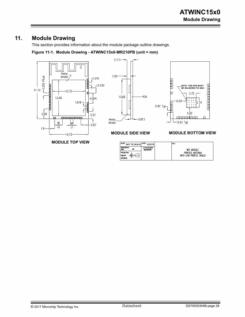
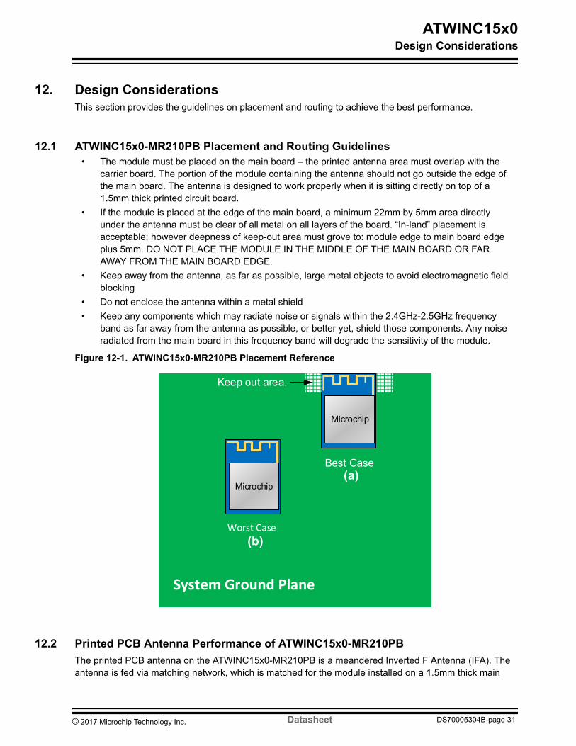

Section Changes
bull Editorial updates
Certification Notices bull Added section for Agency Certificationnotices (now under Regulatory Approvalswith Rev B)
Agency Regulatory Approvals bull Added back Agency Approval sectionbull Revised content of certifications
Reference Documents bull Moved Design File Package to a separateparagraph below the table to remove webavailability aspect and to contact sales
Rev B - 022016
Document bull Updated copyright date to 2016bull Updated footers
Module Outline Drawing bull Revised Module outline drawings to showGround pad to be soldered
bull Pulled out Footprint drawing as this iscovered in the Module drawing
WLAN Subsystem Radio bull Revised Transmit Performance Table 6-3
Power Consumption bull Revised current table references in Table8-1
Schematic Design Information bull Updated Schematics Section 11 text andfigures Figure 11-1 and Figure 11-2
Reflow Profile Information bull Revised section 12 Reflow ProfileInformation
Reference Documents bull Updated Document Reference table toinclude the ATWINC1500-MU datasheet
Rev A - 072015
Document Updated due to changes in the ATWINC1500 fromRev A to Rev B
Description bull Updated model revisions to rev Bbull Corrected Package dimensions
Features bull Added Hardware Accelerator content tofeatures list
Pinout Information bull Updated reference schematic
ATWINC15x0Document Revision History
copy 2017 Microchip Technology Inc Datasheet DS70005304B-page 49
bull New pin list adds GPIOs 345 and 6
CPU and Memory Subsystems bull Increased Memory from 182KB to 160KB
External Interfaces bull Improved and corrected description ofCoexistence interface
bull Editorial updates
Power Consumption bull Updated power numbers and descriptionadded high-power and low-power modes
WLAN Subsystem Radio bull Updated Performance numbers
ATWINC15x0Document Revision History
copy 2017 Microchip Technology Inc Datasheet DS70005304B-page 50
The Microchip Web Site
Microchip provides online support via our web site at httpwwwmicrochipcom This web site is used asa means to make files and information easily available to customers Accessible by using your favoriteInternet browser the web site contains the following information
bull Product Support ndash Data sheets and errata application notes and sample programs designresources userrsquos guides and hardware support documents latest software releases and archivedsoftware
bull General Technical Support ndash Frequently Asked Questions (FAQ) technical support requestsonline discussion groups Microchip consultant program member listing
bull Business of Microchip ndash Product selector and ordering guides latest Microchip press releaseslisting of seminars and events listings of Microchip sales offices distributors and factoryrepresentatives
Customer Change Notification Service
Microchiprsquos customer notification service helps keep customers current on Microchip productsSubscribers will receive e-mail notification whenever there are changes updates revisions or erratarelated to a specified product family or development tool of interest
To register access the Microchip web site at httpwwwmicrochipcom Under ldquoSupportrdquo click onldquoCustomer Change Notificationrdquo and follow the registration instructions
Customer Support
Users of Microchip products can receive assistance through several channels
bull Distributor or Representativebull Local Sales Officebull Field Application Engineer (FAE)bull Technical Support
Customers should contact their distributor representative or Field Application Engineer (FAE) for supportLocal sales offices are also available to help customers A listing of sales offices and locations is includedin the back of this document
Technical support is available through the web site at httpwwwmicrochipcomsupport
Microchip Devices Code Protection Feature
Note the following details of the code protection feature on Microchip devices
bull Microchip products meet the specification contained in their particular Microchip Data Sheetbull Microchip believes that its family of products is one of the most secure families of its kind on the
market today when used in the intended manner and under normal conditionsbull There are dishonest and possibly illegal methods used to breach the code protection feature All of
these methods to our knowledge require using the Microchip products in a manner outside theoperating specifications contained in Microchiprsquos Data Sheets Most likely the person doing so isengaged in theft of intellectual property
bull Microchip is willing to work with the customer who is concerned about the integrity of their code
ATWINC15x0
copy 2017 Microchip Technology Inc Datasheet DS70005304B-page 51
bull Neither Microchip nor any other semiconductor manufacturer can guarantee the security of theircode Code protection does not mean that we are guaranteeing the product as ldquounbreakablerdquo
Code protection is constantly evolving We at Microchip are committed to continuously improving thecode protection features of our products Attempts to break Microchiprsquos code protection feature may be aviolation of the Digital Millennium Copyright Act If such acts allow unauthorized access to your softwareor other copyrighted work you may have a right to sue for relief under that Act
Legal Notice
Information contained in this publication regarding device applications and the like is provided only foryour convenience and may be superseded by updates It is your responsibility to ensure that yourapplication meets with your specifications MICROCHIP MAKES NO REPRESENTATIONS ORWARRANTIES OF ANY KIND WHETHER EXPRESS OR IMPLIED WRITTEN OR ORAL STATUTORYOR OTHERWISE RELATED TO THE INFORMATION INCLUDING BUT NOT LIMITED TO ITSCONDITION QUALITY PERFORMANCE MERCHANTABILITY OR FITNESS FOR PURPOSEMicrochip disclaims all liability arising from this information and its use Use of Microchip devices in lifesupport andor safety applications is entirely at the buyerrsquos risk and the buyer agrees to defendindemnify and hold harmless Microchip from any and all damages claims suits or expenses resultingfrom such use No licenses are conveyed implicitly or otherwise under any Microchip intellectualproperty rights unless otherwise stated
Trademarks
The Microchip name and logo the Microchip logo AnyRate AVR AVR logo AVR Freaks BeaconThingsBitCloud CryptoMemory CryptoRF dsPIC FlashFlex flexPWR Heldo JukeBlox KeeLoq KeeLoq logoKleer LANCheck LINK MD maXStylus maXTouch MediaLB megaAVR MOST MOST logo MPLABOptoLyzer PIC picoPower PICSTART PIC32 logo Prochip Designer QTouch RightTouch SAM-BASpyNIC SST SST Logo SuperFlash tinyAVR UNIO and XMEGA are registered trademarks ofMicrochip Technology Incorporated in the USA and other countries
ClockWorks The Embedded Control Solutions Company EtherSynch Hyper Speed Control HyperLightLoad IntelliMOS mTouch Precision Edge and Quiet-Wire are registered trademarks of MicrochipTechnology Incorporated in the USA
Adjacent Key Suppression AKS Analog-for-the-Digital Age Any Capacitor AnyIn AnyOut BodyComchipKIT chipKIT logo CodeGuard CryptoAuthentication CryptoCompanion CryptoControllerdsPICDEM dsPICDEMnet Dynamic Average Matching DAM ECAN EtherGREEN In-Circuit SerialProgramming ICSP Inter-Chip Connectivity JitterBlocker KleerNet KleerNet logo Mindi MiWimotorBench MPASM MPF MPLAB Certified logo MPLIB MPLINK MultiTRAK NetDetach OmniscientCode Generation PICDEM PICDEMnet PICkit PICtail PureSilicon QMatrix RightTouch logo REALICE Ripple Blocker SAM-ICE Serial Quad IO SMART-IS SQI SuperSwitcher SuperSwitcher II TotalEndurance TSHARC USBCheck VariSense ViewSpan WiperLock Wireless DNA and ZENA aretrademarks of Microchip Technology Incorporated in the USA and other countries
SQTP is a service mark of Microchip Technology Incorporated in the USA
Silicon Storage Technology is a registered trademark of Microchip Technology Inc in other countries
GestIC is a registered trademark of Microchip Technology Germany II GmbH amp Co KG a subsidiary ofMicrochip Technology Inc in other countries
All other trademarks mentioned herein are property of their respective companies
ATWINC15x0
copy 2017 Microchip Technology Inc Datasheet DS70005304B-page 52
copy 2017 Microchip Technology Incorporated Printed in the USA All Rights Reserved
ISBN 978-1-5224-2512-0
Quality Management System Certified by DNV
ISOTS 16949Microchip received ISOTS-169492009 certification for its worldwide headquarters design and waferfabrication facilities in Chandler and Tempe Arizona Gresham Oregon and design centers in Californiaand India The Companyrsquos quality system processes and procedures are for its PICreg MCUs and dsPICreg
DSCs KEELOQreg code hopping devices Serial EEPROMs microperipherals nonvolatile memory andanalog products In addition Microchiprsquos quality system for the design and manufacture of developmentsystems is ISO 90012000 certified
ATWINC15x0
copy 2017 Microchip Technology Inc Datasheet DS70005304B-page 53
AMERICAS ASIAPACIFIC ASIAPACIFIC EUROPECorporate Office2355 West Chandler BlvdChandler AZ 85224-6199Tel 480-792-7200Fax 480-792-7277Technical SupporthttpwwwmicrochipcomsupportWeb AddresswwwmicrochipcomAtlantaDuluth GATel 678-957-9614Fax 678-957-1455Austin TXTel 512-257-3370BostonWestborough MATel 774-760-0087Fax 774-760-0088ChicagoItasca ILTel 630-285-0071Fax 630-285-0075DallasAddison TXTel 972-818-7423Fax 972-818-2924DetroitNovi MITel 248-848-4000Houston TXTel 281-894-5983IndianapolisNoblesville INTel 317-773-8323Fax 317-773-5453Tel 317-536-2380Los AngelesMission Viejo CATel 949-462-9523Fax 949-462-9608Tel 951-273-7800Raleigh NCTel 919-844-7510New York NYTel 631-435-6000San Jose CATel 408-735-9110Tel 408-436-4270Canada - TorontoTel 905-695-1980Fax 905-695-2078
Australia - SydneyTel 61-2-9868-6733China - BeijingTel 86-10-8569-7000China - ChengduTel 86-28-8665-5511China - ChongqingTel 86-23-8980-9588China - DongguanTel 86-769-8702-9880China - GuangzhouTel 86-20-8755-8029China - HangzhouTel 86-571-8792-8115China - Hong Kong SARTel 852-2943-5100China - NanjingTel 86-25-8473-2460China - QingdaoTel 86-532-8502-7355China - ShanghaiTel 86-21-3326-8000China - ShenyangTel 86-24-2334-2829China - ShenzhenTel 86-755-8864-2200China - SuzhouTel 86-186-6233-1526China - WuhanTel 86-27-5980-5300China - XianTel 86-29-8833-7252China - XiamenTel 86-592-2388138China - ZhuhaiTel 86-756-3210040
India - BangaloreTel 91-80-3090-4444India - New DelhiTel 91-11-4160-8631India - PuneTel 91-20-4121-0141Japan - OsakaTel 81-6-6152-7160Japan - TokyoTel 81-3-6880- 3770Korea - DaeguTel 82-53-744-4301Korea - SeoulTel 82-2-554-7200Malaysia - Kuala LumpurTel 60-3-7651-7906Malaysia - PenangTel 60-4-227-8870Philippines - ManilaTel 63-2-634-9065SingaporeTel 65-6334-8870Taiwan - Hsin ChuTel 886-3-577-8366Taiwan - KaohsiungTel 886-7-213-7830Taiwan - TaipeiTel 886-2-2508-8600Thailand - BangkokTel 66-2-694-1351Vietnam - Ho Chi MinhTel 84-28-5448-2100
Austria - WelsTel 43-7242-2244-39Fax 43-7242-2244-393Denmark - CopenhagenTel 45-4450-2828Fax 45-4485-2829Finland - EspooTel 358-9-4520-820France - ParisTel 33-1-69-53-63-20Fax 33-1-69-30-90-79Germany - GarchingTel 49-8931-9700Germany - HaanTel 49-2129-3766400Germany - HeilbronnTel 49-7131-67-3636Germany - KarlsruheTel 49-721-625370Germany - MunichTel 49-89-627-144-0Fax 49-89-627-144-44Germany - RosenheimTel 49-8031-354-560Israel - RarsquoananaTel 972-9-744-7705Italy - MilanTel 39-0331-742611Fax 39-0331-466781Italy - PadovaTel 39-049-7625286Netherlands - DrunenTel 31-416-690399Fax 31-416-690340Norway - TrondheimTel 47-7289-7561Poland - WarsawTel 48-22-3325737Romania - BucharestTel 40-21-407-87-50Spain - MadridTel 34-91-708-08-90Fax 34-91-708-08-91Sweden - GothenbergTel 46-31-704-60-40Sweden - StockholmTel 46-8-5090-4654UK - WokinghamTel 44-118-921-5800Fax 44-118-921-5820
Worldwide Sales and Service
copy 2017 Microchip Technology Inc Datasheet DS70005304B-page 54