Embed Size (px)
Citation preview
Aurore Savoy-Navarro 1), Albert Comerma 2), E. Deumens 3), Thanh Hung Pham 1), Rachid Sefri 1)
1)LPNHE-Université Pierre et Marie Curie/IN2P3-CNRS, Fr2)Universitat de Barcelona Dept d’Estructura i Constituents de la Materia Sp2)Universitat de Barcelona. Dept d Estructura i Constituents de la Materia, Sp
3)IMEC, Leuwen, Be
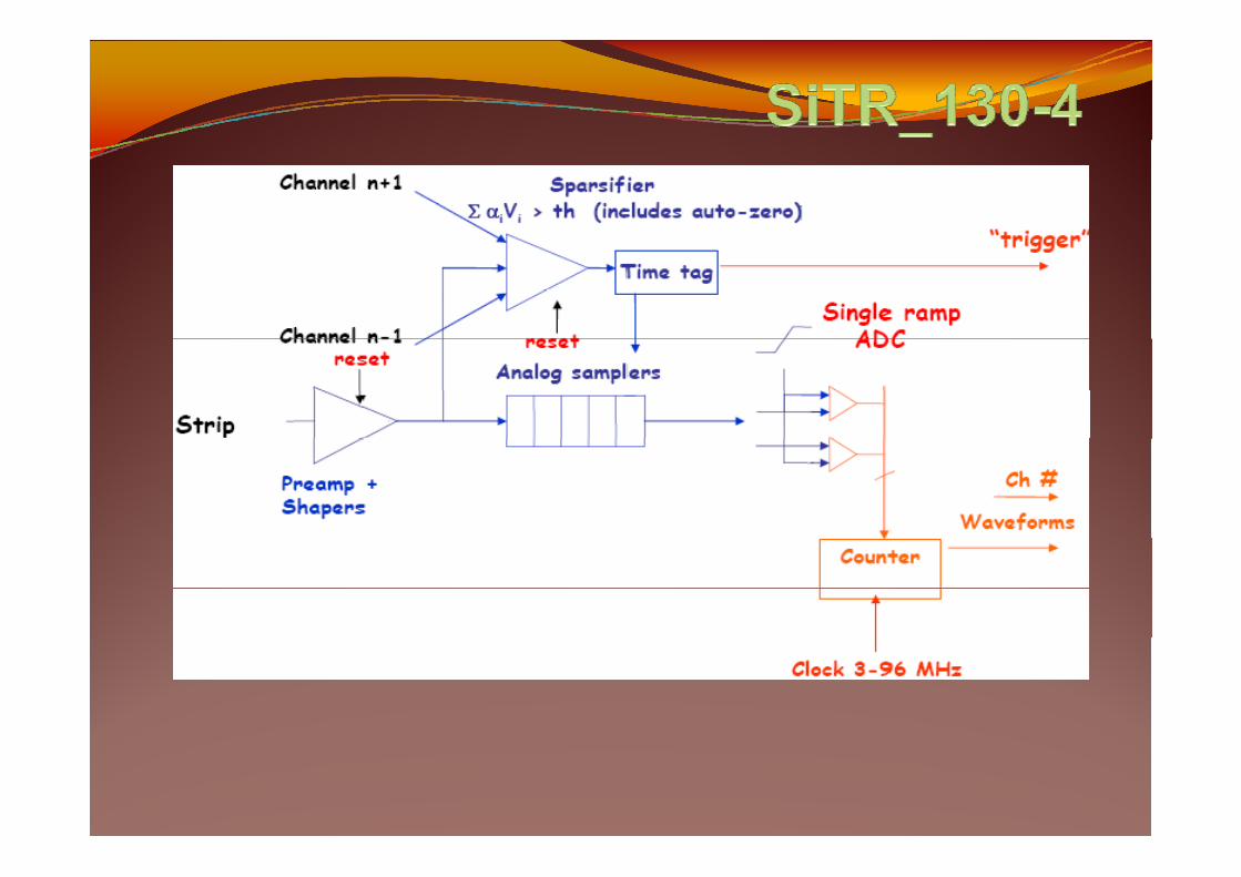
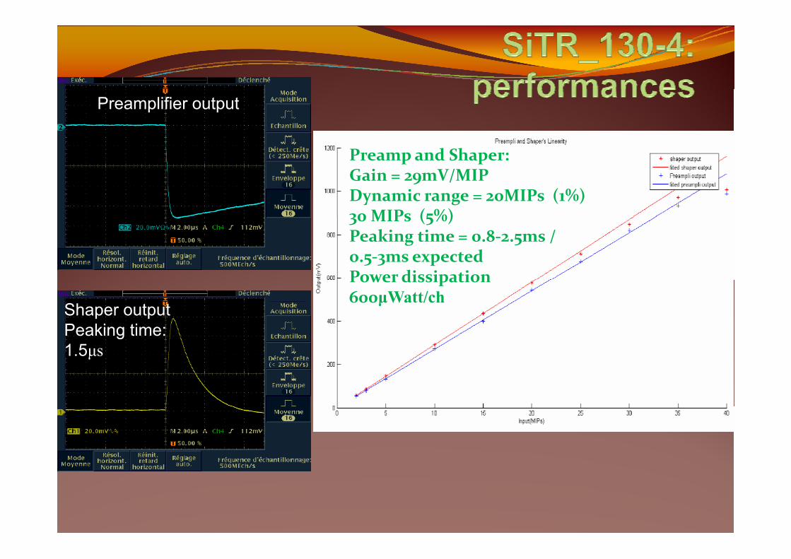
Preamp and Shaper:
Preamplifier output
Preamp and Shaper:Gain = 29mV/MIPDynamic range = 20MIPs (1%)30 MIPs (5%)30 MIPs (5%)Peaking time = 0.8-2.5ms /0.5-3ms expectedPower dissipationPower dissipation600μWatt/ch
Shaper outputPeaking time: 1.5μs
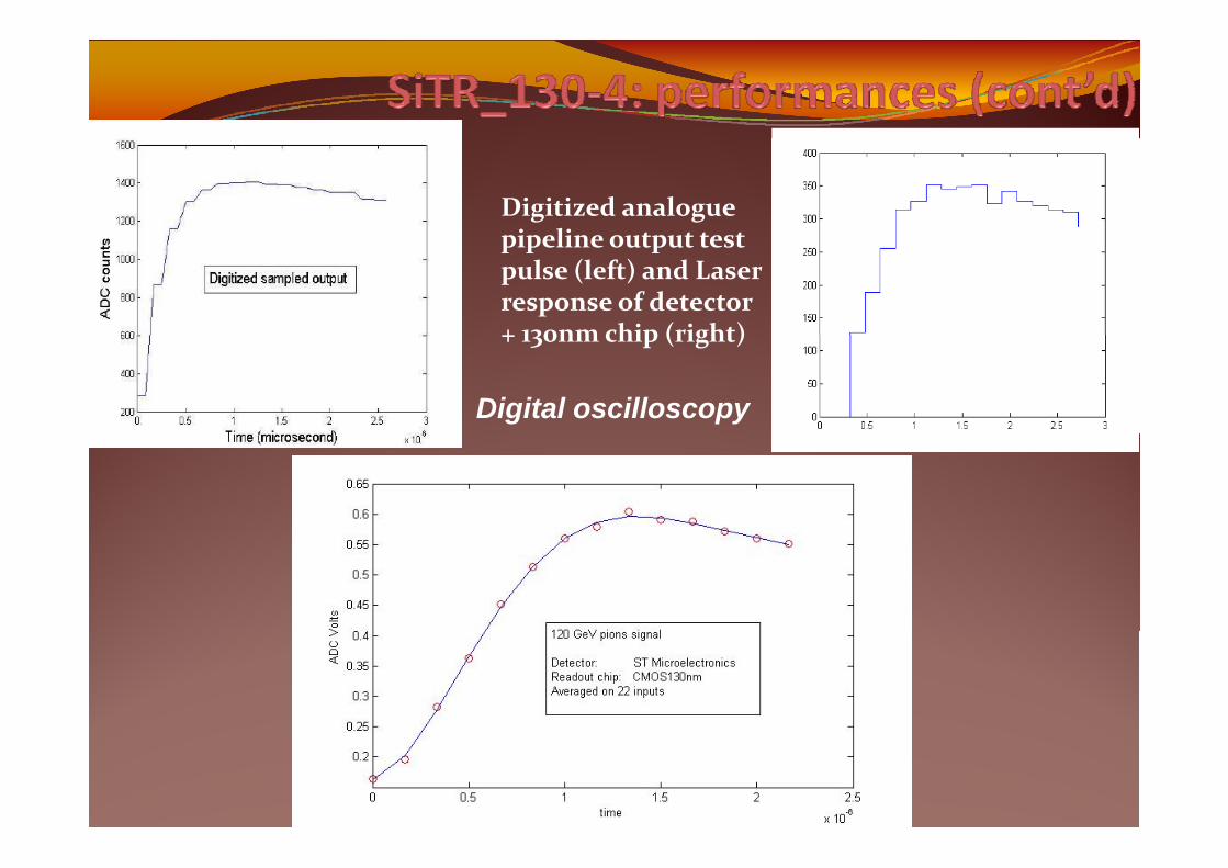
Digitized analogue pipeline output testpipeline output test pulse (left) and Laser response of detector + 130nm chip (right)+ 130nm chip (right)
Digital oscilloscopy
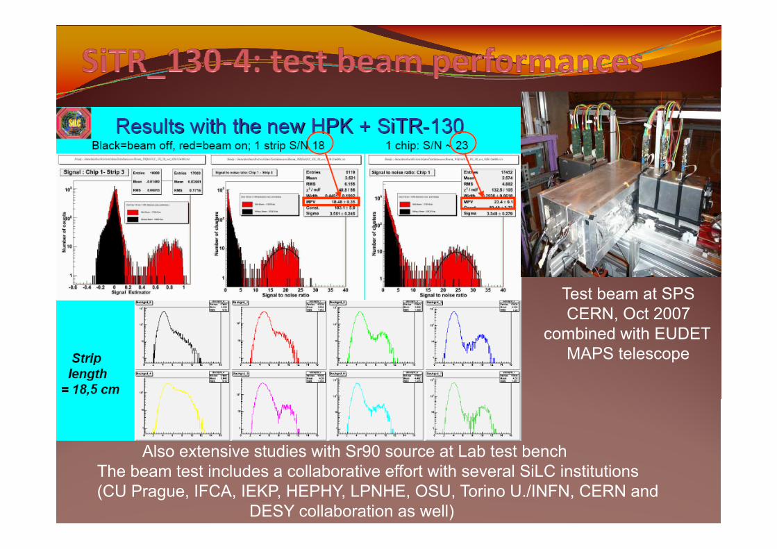
Test beam at SPSCERN, Oct 2007
combined with EUDETcombined with EUDETMAPS telescope
Also extensive studies with Sr90 source at Lab test benchThe beam test includes a collaborative effort with several SiLC institutions(CU Prague, IFCA, IEKP, HEPHY, LPNHE, OSU, Torino U./INFN, CERN and
DESY collaboration as well)
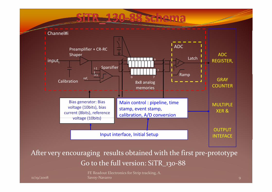
Preamplifier + CR-RC ADC
Channel#i
i-1
i 1i
0
7
Shaper
Sparsifier
Latch
Ramp
ADC REGISTER,inputi
i+10 7refi
8x8 analog memories
RampGRAY
COUNTERCalibration
Bias generator: Bias voltage (10bits), bias
current (8bits), reference voltage (10bits)
MULTIPLEXER &
Main control : pipeline, time stamp, event stamp, calibration, A/D conversion
voltage (10bits)
OUTPUT INTEFACEInput interface, Initial Setup
After very encouraging results obtained with the first pre-prototypeG t th f ll i SiTR 88Go to the full version: SiTR_130-88
11/19/2008 9FE Readout Electronics for Strip tracking, A. Savoy-Navarro
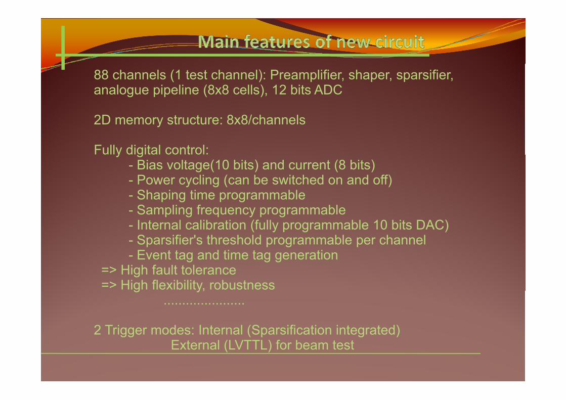
88 channels (1 test channel): Preamplifier, shaper, sparsifier,analogue pipeline (8x8 cells), 12 bits ADC
2D memory structure: 8x8/channels
Fully digital control:y g- Bias voltage(10 bits) and current (8 bits) - Power cycling (can be switched on and off) - Shaping time programmablep g p g- Sampling frequency programmable- Internal calibration (fully programmable 10 bits DAC)- Sparsifier's threshold programmable per channel p p g p- Event tag and time tag generation
=> High fault tolerance=> High flexibility, robustnessg y,
......................
2 Trigger modes: Internal (Sparsification integrated)gg ( p g )External (LVTTL) for beam test
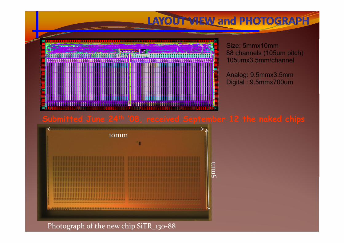
Size: 5mmx10mm88 channels (105um pitch)105umx3.5mm/channel
Analog: 9.5mmx3.5mmDigital : 9.5mmx700um
Submitted June 24th ’08, received September 12 the naked chipsSubmitted June 24 08, received September 12 the naked chips (60), 10mm
5mm
5
Photograph of the new chip SiTR_130-88
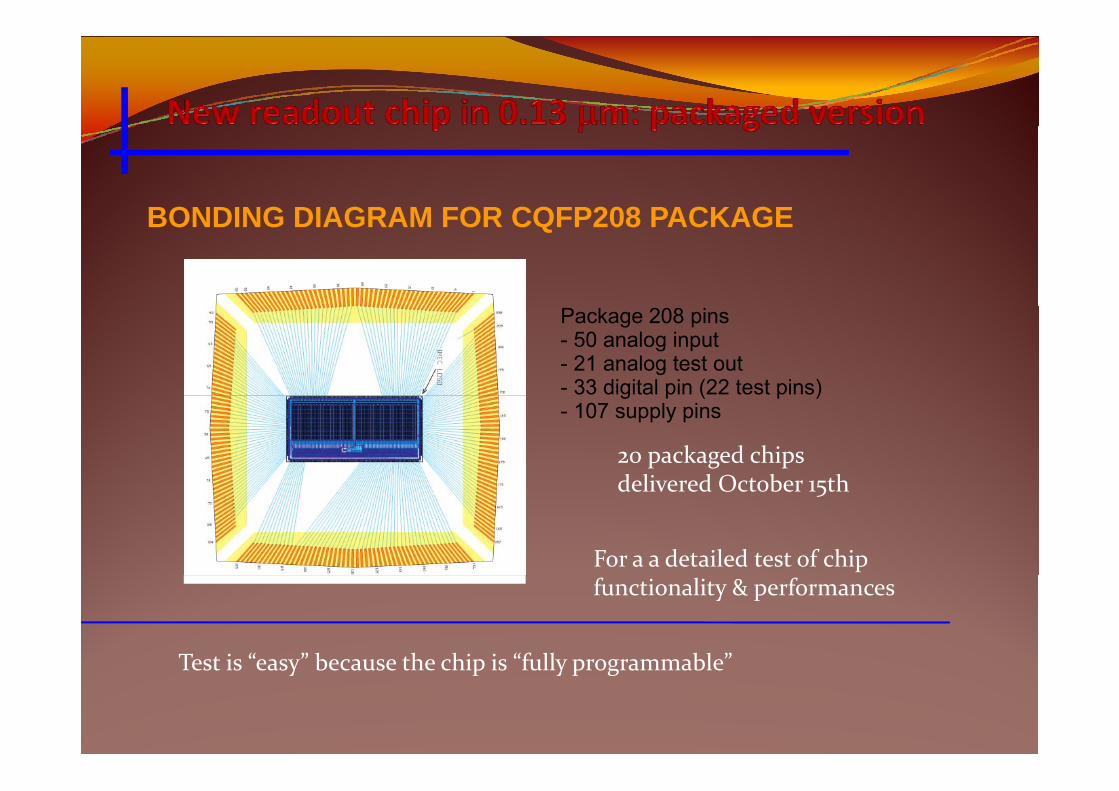
BONDING DIAGRAM FOR CQFP208 PACKAGEBONDING DIAGRAM FOR CQFP208 PACKAGE
Package 208 pins- 50 analog input- 21 analog test out- 33 digital pin (22 test pins)g p ( p )- 107 supply pins
20 packaged chipsdelivered October 15th
For a a detailed test of chip
delivered October 15th
functionality & performances
Test is “easy” because the chip is “fully programmable”Test is easy because the chip is fully programmable

Summary of simulation studiesMain present results from the simualtion studiespPreamplifier:Charge gain: 27mV/MIP 5%Linearity: 17 MIP (1%) to 29 MIP (5%)
Shaper: 30mV/MIP ± 5%Shaping time: 0.5 to 1.5 μsLi i id lifiLinearity: idem premaplifierNoise: 625 + 9 e-/pF (1.5 μs)
Pi li (8 8)Pipeline (8x8)Sampling rate (2)Linearity: idem premaplifier
ADC conversion time: about 85 μs (48 MHhz clock)
Calibration:Calibration: Integrated capacitor: 100 fFCalibration pulse amplitude: 10 bits DAC (same as bias generator)generator)Overall power dissipation per channel: about 1mWatt Total, not including power cycling
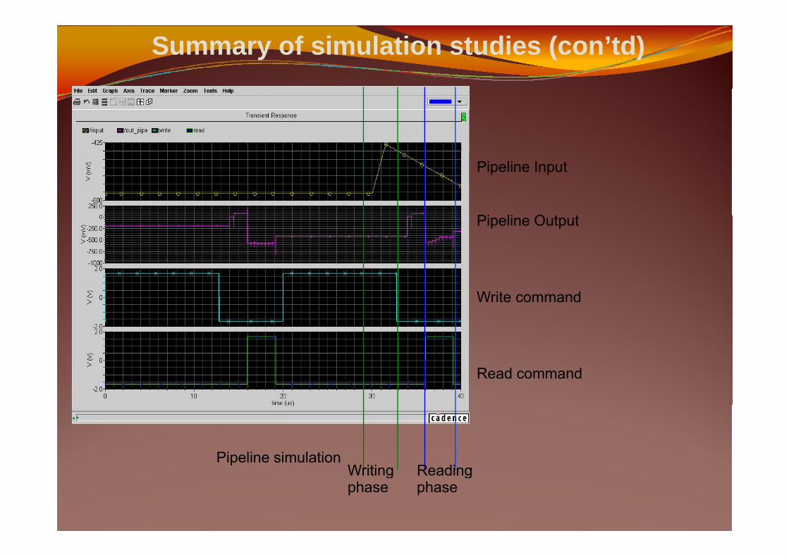
Summary of simulation studies (con’td)
Pipeline Input
Pi li O t tPipeline Output
Write command
Read command
Pipeline simulationWriting ReadingWriting phase
Reading phase

Among the big challenges in designing this chip: to find a way
to perform theto perform themixed mode simulation
Mixed Mode simulation using AMS Designer - Cadence
Analogue
DigitalDigital
Simulation resultYellow : Analogue signalGreen : Digital signal
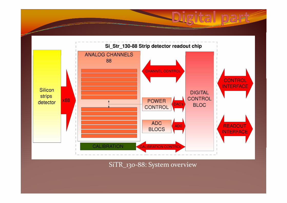
SiTR_130-88: System overview
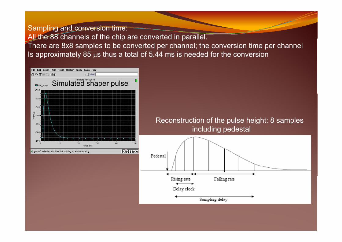
Sampling and conversion time: All the 88 channels of the chip are converted in parallel.All the 88 channels of the chip are converted in parallel.There are 8x8 samples to be converted per channel; the conversion time per channelIs approximately 85 μs thus a total of 5.44 ms is needed for the conversion
Simulated shaper pulse
Reconstruction of the pulse height: 8 samplesReconstruction of the pulse height: 8 samples including pedestal
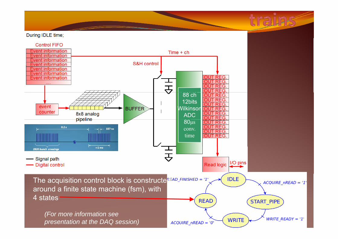
88 ch12bits
WilkinsonADC80μsconv.time
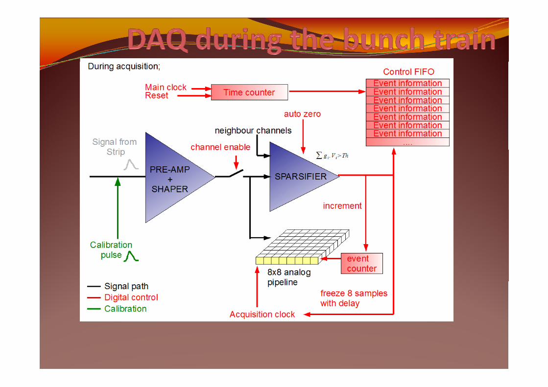
The acquisition control block is constructed around a finite state machine (fsm), with4 states
(For more information see presentation at the DAQ session)
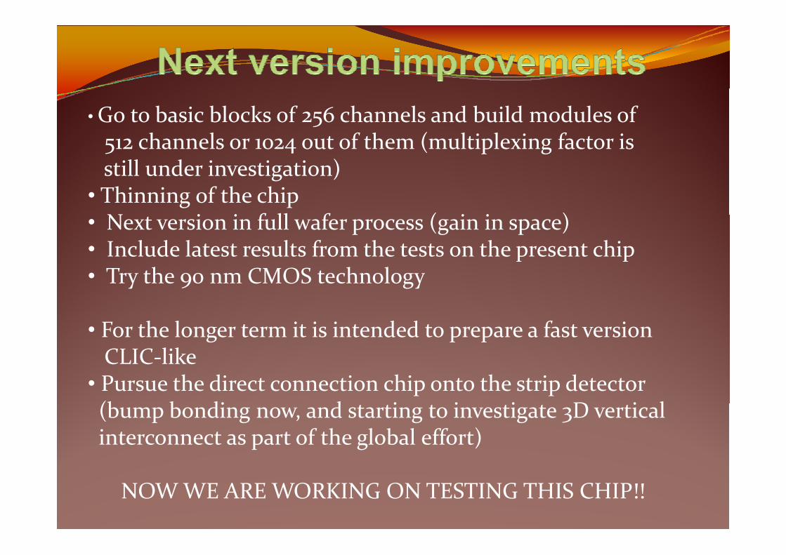
• Go to basic blocks of 256 channels and build modules of 512 channels or 1024 out of them (multiplexing factor is 5 4 ( p gstill under investigation)
• Thinning of the chipN i i f ll f ( i i )• Next version in full wafer process (gain in space)
• Include latest results from the tests on the present chip• Try the 90 nm CMOS technology• Try the 90 nm CMOS technology
• For the longer term it is intended to prepare a fast version g p pCLIC-like
• Pursue the direct connection chip onto the strip detector(b b di d i i i D i l(bump bonding now, and starting to investigate 3D vertical interconnect as part of the global effort)
NOW WE ARE WORKING ON TESTING THIS CHIP!!