Embed Size (px)
Citation preview
AUTOMATED BENCH SETUP FOR TESTING H-BRIDGES
by
VIVEK SHANKARASUBRAHMANYAM, B. E.,
A THESIS
IN
ELECTRICAL ENGINEERING
Submitted to the Graduate Faculty
of Texas Tech University in
Partial Ful�llment of
the Requirements for
the Degree of
MASTER OF SCIENCE
Approved
Dr.Micheal PartenCommittee Chairman
Dr.Richard Gale
Dr. Brian Nutter
Fred HartmeisterDean of the Graduate School
December, 2007

Texas Tech University, Vivek Shankarasubrahmanyam, December 2007
ACKNOWLEDGMENTS
I thank Dr. Parten, Dr.Nutter and Dr.Gale for their interest, support and
valuable suggestions. I want to thank Herb Scott, Nghia Nguyen, S Y Youn, Matt
Roberts, Rambabu Atluri, Gerardo Soriano-Burgos, Randy Straka, Alex Zhou for
guiding me and making it a great learning experience at TI. I want to express my
heart-felt thanks to Poorvaja Kamalapuri, Ganapathy Subramaniam and
Amarnath Kollengude for their relentless support and for always being there.
I acknowledge a real debt of gratitude that I owe to my parents for their
moral encouragement and emotional support. I express my special thanks to
Veena, Vidhya and Vinayak for their con�dence and support.
ii

Texas Tech University, Vivek Shankarasubrahmanyam, December 2007
CONTENTS
ACKNOWLEDGMENTS . . . . . . . . . . . . . . . . . . . . . . . . ii
ABSTRACT . . . . . . . . . . . . . . . . . . . . . . . . . . . . . . . vi
LIST OF FIGURES . . . . . . . . . . . . . . . . . . . . . . . . . . . vii
LIST OF TABLES . . . . . . . . . . . . . . . . . . . . . . . . . . . . ix
I INTRODUCTION . . . . . . . . . . . . . . . . . . . . . . . . . . 1
II CHARACTERIZING H-BRIDGES . . . . . . . . . . . . . . . 4
2.1 CHARACTERIZATION . . . . . . . . . . . . . . . . . . . . . 4
2.1.1 Importance of characterization . . . . . . . . . . . . . . . 4
2.1.1.1 Schedule . . . . . . . . . . . . . . . . . . . . . . . . 4
2.1.1.2 Cost . . . . . . . . . . . . . . . . . . . . . . . . . . . 5
2.1.1.3 Quality . . . . . . . . . . . . . . . . . . . . . . . . . 5
2.2 DC MOTOR DRIVES . . . . . . . . . . . . . . . . . . . . . . 6
2.3 H-BRIDGE . . . . . . . . . . . . . . . . . . . . . . . . . . . . 7
2.4 H-BRIDGE FUNCTIONALITY . . . . . . . . . . . . . . . . . 8
2.5 H-BRIDGE TESTING . . . . . . . . . . . . . . . . . . . . . . 9
2.5.1 Rds(ON) . . . . . . . . . . . . . . . . . . . . . . . . . . . . 10
2.5.2 Leakage current . . . . . . . . . . . . . . . . . . . . . . . . 11
2.5.3 Vfb . . . . . . . . . . . . . . . . . . . . . . . . . . . . . . 12
2.5.4 Vdrop . . . . . . . . . . . . . . . . . . . . . . . . . . . . . 13
2.5.5 Rise time . . . . . . . . . . . . . . . . . . . . . . . . . . . 14
2.5.6 Fall time . . . . . . . . . . . . . . . . . . . . . . . . . . . . 14
2.6 CHARACTERIZATION - ATE . . . . . . . . . . . . . . . . . 15
2.7 CHARACTERIZATION - BENCH SETUP . . . . . . . . . . 16
2.8 IMPORTANCE OF THE PROPOSED SOLUTION . . . . . . 17
iii

Texas Tech University, Vivek Shankarasubrahmanyam, December 2007
2.9 PREVIOUS WORK . . . . . . . . . . . . . . . . . . . . . . . 18
III IMPLEMENTATION OF THE AUTOMATED TEST SO-
LUTION . . . . . . . . . . . . . . . . . . . . . . . . . . . . . . . . 19
3.1 TEST SYSTEM OVERVIEW . . . . . . . . . . . . . . . . . . 19
3.1.1 Instrument Set . . . . . . . . . . . . . . . . . . . . . . . . 20
3.1.1.1 Keithley 2602 (K2602) . . . . . . . . . . . . . . . 20
3.1.1.2 Keithley 2430 . . . . . . . . . . . . . . . . . . . . . 20
3.1.1.3 Agilent 34401 . . . . . . . . . . . . . . . . . . . . . 21
3.1.1.4 Tektronix DPO7054 . . . . . . . . . . . . . . . . . 22
3.1.1.5 GPIB . . . . . . . . . . . . . . . . . . . . . . . . . . 23
3.2 SOFTWARE CONTROL . . . . . . . . . . . . . . . . . . . . 24
3.2.1 Introduction to LabVIEW . . . . . . . . . . . . . . . . . . 24
3.3 DC MODULE . . . . . . . . . . . . . . . . . . . . . . . . . . . 25
3.3.1 Flow Chart . . . . . . . . . . . . . . . . . . . . . . . . . . 32
3.3.2 Test Con�gurations . . . . . . . . . . . . . . . . . . . . . 35
3.4 AC MODULE . . . . . . . . . . . . . . . . . . . . . . . . . . . 36
3.5 SUMMARY . . . . . . . . . . . . . . . . . . . . . . . . . . . . 38
IV DATA AND COST ANALYSIS . . . . . . . . . . . . . . . . . . 43
4.1 TEST RESULTS . . . . . . . . . . . . . . . . . . . . . . . . . 43
4.1.1 Rds(ON) . . . . . . . . . . . . . . . . . . . . . . . . . . . . 44
4.1.2 Leakage . . . . . . . . . . . . . . . . . . . . . . . . . . . . 46
4.1.3 Vdrop . . . . . . . . . . . . . . . . . . . . . . . . . . . . . 48
4.1.4 Vfb . . . . . . . . . . . . . . . . . . . . . . . . . . . . . . 49
4.1.5 Rise Time . . . . . . . . . . . . . . . . . . . . . . . . . . . 50
4.1.6 Fall Time . . . . . . . . . . . . . . . . . . . . . . . . . . . 51
4.2 COST ANALYSIS . . . . . . . . . . . . . . . . . . . . . . . . 52
iv

Texas Tech University, Vivek Shankarasubrahmanyam, December 2007
4.2.1 Test Time . . . . . . . . . . . . . . . . . . . . . . . . . . . 52
4.2.2 Test economics . . . . . . . . . . . . . . . . . . . . . . . . 53
4.2.2.1 Cost Model . . . . . . . . . . . . . . . . . . . . . . 54
4.2.3 Example of test cost . . . . . . . . . . . . . . . . . . . . . 54
4.3 SUMMARY . . . . . . . . . . . . . . . . . . . . . . . . . . . . 57
V CONCLUSION . . . . . . . . . . . . . . . . . . . . . . . . . . . . 58
5.1 FUTURE WORK . . . . . . . . . . . . . . . . . . . . . . . . . 59
BIBLIOGRAPHY . . . . . . . . . . . . . . . . . . . . . . . . . . . . . . . 60
v
Texas Tech University, Vivek Shankarasubrahmanyam, December 2007
ABSTRACT
Characterization is an important step before integrated circuits are produced
for sale. Characterizing is expensive and time-consuming. This paper analyzes the
methods of characterizing and proposes an alternate solution that is not as
expensive as testing on an ATE and is very fast when compared to characterizing
on a bench setup. The solution involves automating the testing procedure on a
bench setup. The programming to control the instruments is accomplished in
LabVIEW. The data from the tests are analyzed for repeatability. A cost estimate
is also developed to aid in determining the ideal testing method for di�erent
requirements.
vi

Texas Tech University, Vivek Shankarasubrahmanyam, December 2007
LIST OF FIGURES
2.1 H-Bridge . . . . . . . . . . . . . . . . . . . . . . . . . . . . . . . . . . 7
2.2 H-Bridge with positive voltage across the motor terminals . . . . . . 8
2.3 H-Bridge with negative voltage across the motor terminals . . . . . . 9
2.4 Circuit diagram of an H-Bridge . . . . . . . . . . . . . . . . . . . . . 10
2.5 Schematic: Circuit used to measure Rds(ON) . . . . . . . . . . . . . . 11
2.6 Schematic: Circuit used to measure leakage current . . . . . . . . . . 12
2.7 Schematic: Circuit used to measure Vfb . . . . . . . . . . . . . . . . 13
2.8 Schematic: Circuit used to measure rise and fall time . . . . . . . . . 15
3.1 Test system overview . . . . . . . . . . . . . . . . . . . . . . . . . . . 19
3.2 Structure of the program . . . . . . . . . . . . . . . . . . . . . . . . 26
3.3 DC module front-panel: Inner loop . . . . . . . . . . . . . . . . . . . 27
3.4 Block diagram: Writing values to the instruments . . . . . . . . . . . 28
3.5 Block diagram: Enabling external DMM . . . . . . . . . . . . . . . . 29
3.6 Block diagram: Creating new �le names . . . . . . . . . . . . . . . . 30
3.7 Block diagram: Function of follow setup PreDIO en . . . . . . . . 31
3.8 DC front panel: IO Spec cluster . . . . . . . . . . . . . . . . . . . . 32
3.9 Block diagram: Functioning of IO Spec EN . . . . . . . . . . . . . . 32
3.10 Test program ow chart . . . . . . . . . . . . . . . . . . . . . . . . . 39
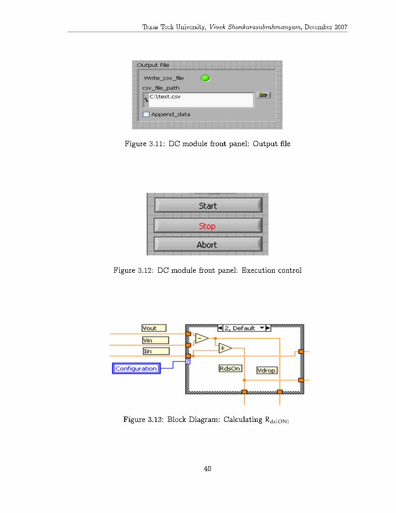
3.11 DC module front panel: Output �le . . . . . . . . . . . . . . . . . . 40
3.12 DC module front panel: Execution control . . . . . . . . . . . . . . . 40
3.13 Block Diagram: Calculating Rds(ON) . . . . . . . . . . . . . . . . . . 40
3.14 AC module Front panel . . . . . . . . . . . . . . . . . . . . . . . . . 41
3.15 Block diagram: Read the scope . . . . . . . . . . . . . . . . . . . . . 41
3.16 Block diagram: GPIB Write . . . . . . . . . . . . . . . . . . . . . . 42
vii
Texas Tech University, Vivek Shankarasubrahmanyam, December 2007
3.17 Block diagram: Index array block retrieving rise time from the out-
put bu�er . . . . . . . . . . . . . . . . . . . . . . . . . . . . . . . . . 42
4.1 Distribution: Rds(ON) Characterization: 33 devices, 0.6 A, 0.8 A and
1.0 A, 2.74 V and 5.2 V . . . . . . . . . . . . . . . . . . . . . . . . . 45
4.2 Distribution: Rds(ON) for a device tested 30 times . . . . . . . . . . . 46
4.3 Distribution: Leakage for 34 devices at three di�erent voltages . . . 47
4.4 Distribution: Leakage current on the same device tested 35 times . . 48
4.5 Distribution: Vdrop tested on 30 devices . . . . . . . . . . . . . . . . 48
4.6 Distribution: Vdrop values of the same device tested 30 times . . . . 49
4.7 Distribution: Vfb for di�erent currents . . . . . . . . . . . . . . . . . 50
4.8 Distribution: Vfb for the same device tested 35 times . . . . . . . . . 51
4.9 Distribution: Rise times for di�erent voltage values . . . . . . . . . . 51
4.10 Distribution: Rise times for the same device tested 30 times . . . . . 52
4.11 Distribution: Fall times for di�erent voltage values . . . . . . . . . . 52
4.12 Distribution: Fall times for same device test 30 times . . . . . . . . 53
4.13 Cost comparison: ATE vs. automated bench . . . . . . . . . . . . . 56
4.14 Cost comparison: Bench vs. automated bench . . . . . . . . . . . . . 56
viii
Texas Tech University, Vivek Shankarasubrahmanyam, December 2007
LIST OF TABLES
3.1 Condensed speci�cations of Keithley 2602 . . . . . . . . . . . . . . . 21
3.2 Keithley 2430 voltage and current programming accuracy . . . . . . 22
3.3 Measurement accuracy of Keithley 2430 . . . . . . . . . . . . . . . . 23
3.4 Agilent DMM - DC Voltage measurement accuracy . . . . . . . . . . 23
4.1 Rds(ON) values at di�erent conditions . . . . . . . . . . . . . . . . . . 45
4.2 Leakage current on 30 devices . . . . . . . . . . . . . . . . . . . . . . 47
4.3 Vdrop test for 30 devices . . . . . . . . . . . . . . . . . . . . . . . . . 49
4.4 Vfb : Mean and standard deviation for di�erent currents . . . . . . . 50
4.5 Cost assumptions . . . . . . . . . . . . . . . . . . . . . . . . . . . . . 55
4.6 Test cost for di�erent test techniques . . . . . . . . . . . . . . . . . . 55
ix
Texas Tech University, Vivek Shankarasubrahmanyam, December 2007
CHAPTER 1
INTRODUCTION
The semiconductor industry is one of the fastest growing industries.
Integrated chip (IC) solutions to di�erent problems are gaining momentum and
are evidenced by the increasing use of electronic products in everyday life. Today,
circuits with a remarkable level of complexity can be developed within a small
physical package. Since the demonstration of the transistor by Bardeen, Brattain,
and Shockley at Bell Laboratories (1947), analog circuit design has evolved from
using merely few tens of transistors to placing multiple electronic devices on the
same substrate. The technology has moved from producing simple circuits to
memories containing a billion transistors and microprocessors comprising of more
than 10 million devices [1, 2].
"The complexity for minimum component costs has increased at a rate
of roughly a factor of two per year. Certainly over the short term this
rate can be expected to continue, if not to increase. Over the longer
term, the rate of increase is a bit more uncertain, although there is no
reason to believe it will not remain nearly constant for at least 10 years.
That means by 1975, the number of components per integrated circuit
for minimum cost will be 65,000. I believe that such a large circuit can
be built on a single wafer. [3]" - Gordon E. Moore
Moore's law [3] held for more than ten years. It has become a standard that
the semi-conductor industry is trying to uphold. The actual number of transistors
has continued to double every 18 months, and the dimension of the transistors has
dropped from about 25 m in 1960 to about 0.18 m in 2000, resulting in
tremendous increase in the speed of the ICs [2].
1

Texas Tech University, Vivek Shankarasubrahmanyam, December 2007
IC developing and manufacturing consists of design, fabrication and test.
The design phase consists of converting a set of speci�cations, requirements, or
descriptions of IC operation furnished by a customer into a working circuit [4].
Fabrication involves translating a circuit design into a physical IC using a
quali�ed fabrication process. This yields a wafer level or a fully packaged device
[1]. The test activity ensures that the fabricated circuit meets the required set of
performance standards [5, 6, 7].
ICs are fabricated using a series of photographic printing, etching,
implanting and chemical vapor deposition [8]. Cross sections of the actual
integrated circuits reveal a variety of non-ideal physical characteristics. These
characteristics are often not under the control of the manufacturer. However, they
may have profound e�ects on the circuit characteristics [7]. Thus, the ICs must be
tested before being shipped to the customer. The electronics industry tests the
ICs before they go on a circuit board and then once again test the board before
they are assembled into larger systems. This is because the experience in
electronic testing has shown that the cost increases by tenfold every time a faulty
item is not detected but is used to form a larger electronic circuit or system [7].
Hence, testing is done at various stages of the IC development procedure. It
includes simulation, veri�cation/characterization, production test and failure
analysis [1]. Characterization involves exhaustively testing the IC under all
conditions to determine the device's functional and parametric capabilities.
Characterization leads to a comprehensive understanding of the device behavior.
It also helps the design engineers to identify and correct marginal portions of the
design. Further, the data collected from the characterization tests could help the
test engineers determine the worst-case test conditions that can be tested in the
production test program, because complete device characterization tests are not
2
Texas Tech University, Vivek Shankarasubrahmanyam, December 2007
cost-e�ective in a production test program.
Test economics has been receiving considerable attention, because in large
electronic systems, testing accounts for one third of the cost. Further, testing has
a complex relation with quality. Costs include the cost of automatic test
equipment (ATE), the cost of test development, and the cost of "design for
testability" [6]. Testing is expensive. Intel recently reported that the combination
of veri�cation testing and manufacturing testing is its major capital cost [6].
Characterization of a device is time-consuming. Doing a complete
characterization on an ATE would be very expensive. Bench testing the devices
for all conditions is cumbersome [8]. Thus, an alternate solution to this problem is
necessary.
The second chapter describes the problem in more detail. It also gives an
overview of the time and cost factors in testing. It goes on to explain the
opportunity for an alternate to the existing solution to address the problem.
Chapter 3 details the solution that has been proposed. It gives an
introduction to LabVIEW [9] and automated bench testing. It includes the list of
tests that were implemented in LabVIEW. It also includes the list of instruments
that were used for pilot testing the program.
The data collected with the automated bench setup is analyzed in chapter 4.
The chapter 4 also includes an example of the cost involved in implementing this
system. Chapter 5 summarizes the work and lists the advantages of one system
over the other.
3

Texas Tech University, Vivek Shankarasubrahmanyam, December 2007
CHAPTER 2
CHARACTERIZING H-BRIDGES
2.1 CHARACTERIZATION
Characterization of an integrated circuit is also known as design debug or
veri�cation test. It is done prior to producing the part for sale. It aids in design
veri�cation and to determine if the device meets all speci�cations. Comprehensive
AC and DC measurements are made during characterization. A complete
functional test is also included. Characterization testing determines the exact
limits of the device. The test is carried out on a statistically signi�cant sample of
devices and is repeated for every combination of two or more variables. The data
accumulated from these tests can then be used to correct design aws, set �nal
speci�cations and develop the production test program [6].
The production test can be a subset of the characterization tests. From the
characterization tests, worst-case conditions can be determined, and production
tests can be developed to cover these conditions.
2.1.1 Importance of characterization
Veri�cation has become a major challenge in the development of integrated
circuits. Any integrated circuit development process has three major constraints.
2.1.1.1 Schedule
The market for integrated circuits (ICs) is very sensitive to when it is
available to customers. ICs must hit the market at the right time. In the
semiconductor industry, a disproportionate amount of the revenue goes to the
product that is the �rst available in the market place. Hence, schedule is a major
4

Texas Tech University, Vivek Shankarasubrahmanyam, December 2007
constraint.
2.1.1.2 Cost
Every company strives to keep development costs to a minimum. A reduced
cost translates into increased pro�t and / or greater marketability. If a design aw
or marginality is not detected in the veri�cation phase, it could lead to a reduced
yield in production. Discovering design marginality during the production phase
can lead to redesign and/or fabrication changes. These changes are expensive and
time-consuming. Further, these delays could lead to the company getting a bad
reputation; hence, a�ecting the sales of future devices as well.
2.1.1.3 Quality
Products delivered to the customer should meet a required standard of
quality. A compromise in the quality of a device can have a devastating e�ect on
the company.
All three constraints are inter-dependent. For instance, maximizing quality
could mean spending more time / resources on device testing which translates into
increased cost. Similarly, maximizing quality with no attention to the schedule
could translate into increased production cost. Hence, it is very pertinent to �nd a
balance between good quality, schedule and reduced cost. Further, as mentioned
previously, each undetected aw would grow with time. A problem uncovered
early in the characterization phase will cost less to �x. However, if the problem is
allowed to permeate into a larger circuit, it would cost a lot more to �x. Finally, a
customer discovering a problem may tarnish the reputation of the company.
Characterization a�ects all three constraints. An IC can be fabricated and
marketed sooner, if a characterization team is able to remove errors quickly and
e�ciently. Further, the additional cost that is incurred with each additional
5

Texas Tech University, Vivek Shankarasubrahmanyam, December 2007
fabrication can drive development cost and negatively impact the product
schedule. A good characterization can reduce the number of changes to the design
and fabrication process. It can also identify marginality in the design, which if left
unchecked could surface in the customer's environment and cause quality
problems. Spending time and resources on design characterization is justi�ed
because of its e�ect on the three vital constraints indicated [10].
Characterization procedures are usually the same for a given functional unit.
For instance, if the company develops integrated circuits that go in various types
of printers, it is very reasonable to expect many of the integrated circuits to have
motor driver circuits in them. Furthermore, it is also reasonable to expect the
characterization procedure to be the same for most of the motor drivers. Motor
drivers may be rated di�erently or sometimes have additional capabilities.
However, the essential method of testing each parameter is usually very similar.
2.2 DC MOTOR DRIVES
An increasing number of applications require motor drivers in an integrated
circuit. Typical examples include digital cameras, printers etc. It is common to
have one or more motor drives in an integrated circuit.
The general requirement in DC motors is the facility to control speed and
torque. Hence the motor power can be controlled by varying the speed and torque
of the motor. Voltage can be used to control the speed of the DC motor. With the
availability of wide range of power MOSFETs, the drive power can be usefully
spanned from a few watts to tens of kilowatts. Power MOSFETs require a low
gate current, which can be directly obtained from CMOS integrated circuits. For
low-speed high-torque operation, pulse width modulation is a valuable technique
[11, 12]. A simple switch can be used to drive a motor. To control the speed of
6
Texas Tech University, Vivek Shankarasubrahmanyam, December 2007
the motor, the switch can be rapidly pulsed ON and OFF. This action powers the
motor in short bursts and allows for varying speeds.
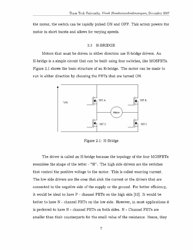
2.3 H-BRIDGE
Motors that must be driven in either direction use H-bridge drivers. An
H-bridge is a simple circuit that can be built using four switches, like MOSFETs.
Figure 2.1 shows the basic structure of an H-bridge. The motor can be made to
run in either direction by choosing the FETs that are turned ON.
Figure 2.1: H-Bridge
The driver is called an H-bridge because the topology of the four MOSFETs
resembles the shape of the letter - "H". The high side drivers are the switches
that control the positive voltage to the motor. This is called sourcing current.
The low side drivers are the ones that sink the current or the drivers that are
connected to the negative side of the supply or the ground. For better e�ciency,
it would be ideal to have P - channel FETs on the high side [12]. It would be
better to have N - channel FETs on the low side. However, in most applications it
is preferred to have N - channel FETs on both sides. N - Channel FETs are
smaller than their counterparts for the small value of the resistance. Hence, they
7
Texas Tech University, Vivek Shankarasubrahmanyam, December 2007
save the silicon area on the integrated circuits.
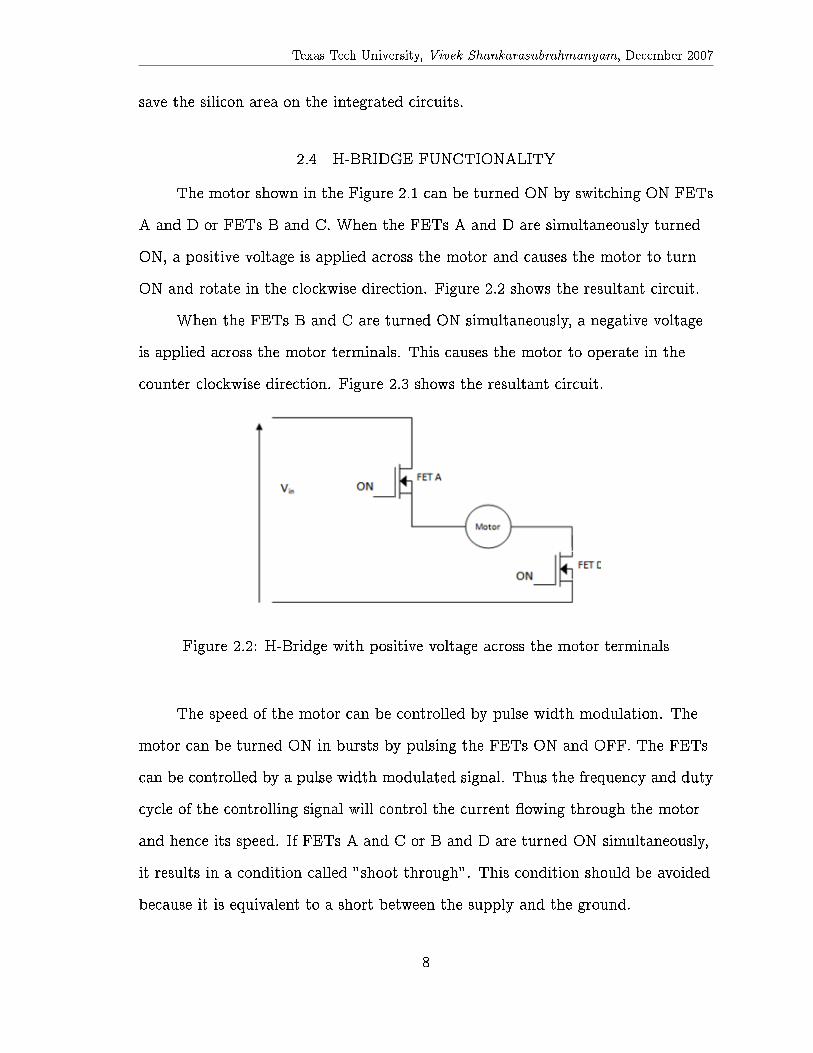
2.4 H-BRIDGE FUNCTIONALITY
The motor shown in the Figure 2.1 can be turned ON by switching ON FETs
A and D or FETs B and C. When the FETs A and D are simultaneously turned
ON, a positive voltage is applied across the motor and causes the motor to turn
ON and rotate in the clockwise direction. Figure 2.2 shows the resultant circuit.
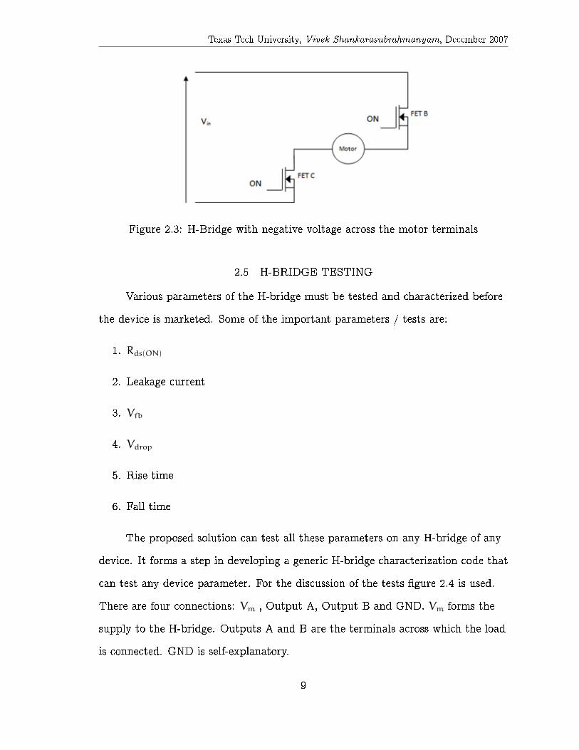
When the FETs B and C are turned ON simultaneously, a negative voltage
is applied across the motor terminals. This causes the motor to operate in the
counter clockwise direction. Figure 2.3 shows the resultant circuit.
Figure 2.2: H-Bridge with positive voltage across the motor terminals
The speed of the motor can be controlled by pulse width modulation. The
motor can be turned ON in bursts by pulsing the FETs ON and OFF. The FETs
can be controlled by a pulse width modulated signal. Thus the frequency and duty
cycle of the controlling signal will control the current owing through the motor
and hence its speed. If FETs A and C or B and D are turned ON simultaneously,
it results in a condition called "shoot through". This condition should be avoided
because it is equivalent to a short between the supply and the ground.
8
Texas Tech University, Vivek Shankarasubrahmanyam, December 2007
Figure 2.3: H-Bridge with negative voltage across the motor terminals
2.5 H-BRIDGE TESTING
Various parameters of the H-bridge must be tested and characterized before
the device is marketed. Some of the important parameters / tests are:
1. Rds(ON)
2. Leakage current
3. Vfb
4. Vdrop
5. Rise time
6. Fall time
The proposed solution can test all these parameters on any H-bridge of any
device. It forms a step in developing a generic H-bridge characterization code that
can test any device parameter. For the discussion of the tests �gure 2.4 is used.
There are four connections: Vm , Output A, Output B and GND. Vm forms the
supply to the H-bridge. Outputs A and B are the terminals across which the load
is connected. GND is self-explanatory.
9

Texas Tech University, Vivek Shankarasubrahmanyam, December 2007
Figure 2.4: Circuit diagram of an H-Bridge
2.5.1 Rds(ON)
Rds(ON) is de�ned as the resistance between the drain and the source of a
MOSFET when it is turned ON. As the value of Rds(ON) increases, the heat
dissipation and the power consumption of the FET also increase. This increase is
undesirable, and hence this resistance is required to remain under a maximum
limit [13].
Test procedure:
(i) Turn ON the FET
(ii) Force known current through the FET
(iii) Measure voltage drop across the FET
(iv) Divide the voltage drop by the current forced to calculate Rds(ON)
Rds(ON) can be characterized for various values of current and the supply
10

Texas Tech University, Vivek Shankarasubrahmanyam, December 2007
voltage. Figure 2.5 shows the schematic of a circuit that is used to measure
Rds(ON) . The actual circuit used may vary based on the device. The instruments
used to make the measurements are explained in the third chapter.
Figure 2.5: Schematic: Circuit used to measure Rds(ON)
2.5.2 Leakage current
Leakage is the current that leaks through a FET when it is turned OFF.
Ideally, leakage current should be zero. However, a leakage current in the order of
nano-amperes is usually measured in all FETs. Leaky FETs lead to increased
power consumption even in the quiescent state and are undesirable.
Test procedure:
(i) Make sure the FET is turned OFF
(ii) Apply Vm, the supply voltage, to the H-bridge show in the Figure 2.4
(iii) Measure the current owing through the FET
Leakage current can be characterized for various values of Vds. Figure 2.6
shows the schematic of a circuit that is used to measure leakage current. The
11

Texas Tech University, Vivek Shankarasubrahmanyam, December 2007
actual circuit used may vary based on the device. The instruments used to make
the measurements are explained in the third chapter.
Figure 2.6: Schematic: Circuit used to measure leakage current
2.5.3 Vfb
Forward bias body diode voltage is de�ned as the voltage drop between the
drain and the substrate. When the drain is shorted to the ground, the voltage
drop across the drain and the source gives a measure of the voltage drop between
the source and the substrate.
Test procedure:
(i) Turn OFF the H-bridge FETs
(ii) Short Vm to ground
(iii) Force current through the output
(iv) Measure voltage drop between drain and source
The current that is being forced through the output can be varied. Figure
2.7 shows the schematic of a circuit that is used to measure Vfb . The actual
12
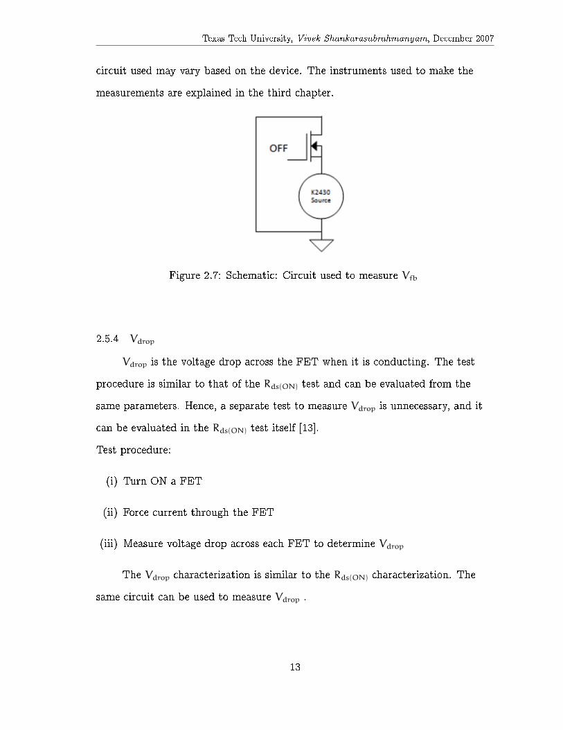
Texas Tech University, Vivek Shankarasubrahmanyam, December 2007
circuit used may vary based on the device. The instruments used to make the
measurements are explained in the third chapter.
Figure 2.7: Schematic: Circuit used to measure Vfb
2.5.4 Vdrop
Vdrop is the voltage drop across the FET when it is conducting. The test
procedure is similar to that of the Rds(ON) test and can be evaluated from the
same parameters. Hence, a separate test to measure Vdrop is unnecessary, and it
can be evaluated in the Rds(ON) test itself [13].
Test procedure:
(i) Turn ON a FET
(ii) Force current through the FET
(iii) Measure voltage drop across each FET to determine Vdrop
The Vdrop characterization is similar to the Rds(ON) characterization. The
same circuit can be used to measure Vdrop .
13

Texas Tech University, Vivek Shankarasubrahmanyam, December 2007
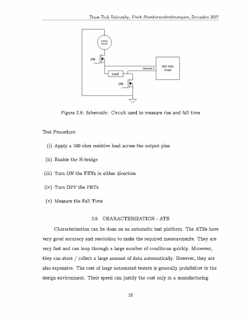
2.5.5 Rise time
The output rise time is de�ned as the time taken for the output to rise from
10% of the original value to 90% of the desired value when the motor is turned
ON. The rise time gives an indication of the FET's response time to being
switched ON. It indirectly a�ects other parameters [13]. In the case of reactive
loads, the rise time also determines the e�ciency, because power is lost in the
transistor while switching.
Test procedure:
(i) Apply a 100 ohm resistive load across the output pins.
(ii) Enable the H-bridge
(iii) Turn ON the FETs in either direction
(iv) Measure the rise time
The rise time can be measured using the circuit shown in Figure 2.8. The
instruments used to make the measurements are explained in the third chapter.
The actual circuit may vary based on the device being tested.
2.5.6 Fall time
The output fall time is de�ned as the time taken for the output to fall from
90% of the ON state to 10% of the OFF state when the motor is being turned
OFF. This parameter restores the FET to its original non-conducting state, with
full drain voltage and no current owing. As in the case of the rise time, the fall
time also determines the e�ciency of the drive, esp. with reactive loads [13]. The
circuit needed to measure fall time is the same as that used to measure rise time.
14
Texas Tech University, Vivek Shankarasubrahmanyam, December 2007
Figure 2.8: Schematic: Circuit used to measure rise and fall time
Test Procedure:
(i) Apply a 100 ohm resistive load across the output pins
(ii) Enable the H-bridge
(iii) Turn ON the FETs in either direction
(iv) Turn OFF the FETs
(v) Measure the Fall Time
2.6 CHARACTERIZATION - ATE
Characterization can be done on an automatic test platform. The ATEs have
very good accuracy and resolution to make the required measurements. They are
very fast and can loop through a large number of conditions quickly. Moreover,
they can store / collect a large amount of data automatically. However, they are
also expensive. The cost of large automated testers is generally prohibitive in the
design environment. Their speed can justify the cost only in a manufacturing
15

Texas Tech University, Vivek Shankarasubrahmanyam, December 2007
environment. For characterization, it turns out to be very expensive. System
rental is also expensive - $100 to $125 per hour [14]. ATE systems also have the
disadvantage of being remote to the designer.
For instance, in the case of Rds(ON) characterization there may be 2 variables
that may need to be varied: the current sourced and the supply voltage. If
characterization plan involves looping 10 di�erent supply voltages at 10 di�erent
current levels, the ATE might have to do an Rds(ON) measurement 100 times. If it
takes 200 ms to make a single measurement and 100 ms to cool down between
successive measurements, the total test time needed to characterize one FET for
one parameter would be 30 seconds.
The exact test cost is estimated based on various factors like initial cost,
average power usage, tester life cycle, etc. The test cost would increase
dramatically if all the FETs were considered and all other parameters are
included. Further, if the test needs to be repeated at di�erent temperatures the
test cost would be very high. Moreover, if the company intends to outsource
testing and fabrication to an external business unit and still maintain quality by
periodically testing / characterizing few circuits, it need not have an ATE for
testing. More explanation of test cost is included in the fourth chapter.
A �nal disadvantage of the ATE equipment is that they are built primarily
to make yes or no decisions and not make detailed parametric studies [14].
2.7 CHARACTERIZATION - BENCH SETUP
Characterization is normally done using a bench setup. In this case, the test
engineer formulates the characterization plan, including a complete instruction set
for a technician to follow to collect data. The expensive ATE equipment is
bypassed in this case. The testing is accomplished using sources, oscilloscopes and
16
Texas Tech University, Vivek Shankarasubrahmanyam, December 2007
measuring instruments that are available in the laboratory. However, this
approach has a number of disadvantages. First, the data collection is manual and
hence error-prone. Second, because the instruments are manually operated, there
is no control on the amount of stress that a device undergoes while being tested.
Third, the characterization is time consuming.
Consider the previous scenario of characterizing a FET for the Rds(ON)
parameter. It might take a person about 30 seconds to make one measurement.
Hence characterizing the Rds(ON) for a FET would take up to an hour. When all
FETs in the device are taken into consideration, the time taken to characterize a
single parameter would balloon.
Manually testing a device is not easily repeatable. For instance, while taking
measurement of the Rds(ON) at high currents, the technician might accidently
over-stress the part. This may lead to an altered behavior in the future tests by
the same device.
Moreover, a statistically signi�cant number of devices must be tested to be
able to make any decision about the device functionality. Hence, characterizing
the devices using a bench setup is lengthy.
The device is subjected to manual handling during the bench test. The
human handling could damage the device.
2.8 IMPORTANCE OF THE PROPOSED SOLUTION
The proposed solution to device characterization forms an alternative to
slow bench testing or expensive ATE characterization. It involves automating the
testing procedure on the bench by controlling the instruments with a computer
using LabVIEW [9]. The program is designed to run with minimum or no
supervision from technicians.
17
Texas Tech University, Vivek Shankarasubrahmanyam, December 2007
The most prominent disadvantage of bench characterization is the time taken
to complete a statistically signi�cant number of tests. This time can be drastically
reduced by controlling the testing instruments using a computer and automating
the testing procedure. Further, the automation also leads to better reliability,
greater repeatability and accurate data collection and easy data storage.
Characterizing on an ATE has many advantages. However, the capital costs
for these testers are high. Further specialized test engineers are required to
characterize each device. Automating the bench procedure would signi�cantly
reduce eliminate the initial costs.
Moreover, the proposed solution is a generic program that can be re-used for
future devices with minimum changes. Additionally, more tests can be included
very easily to the existing program to measure di�erent parameters.
Further, the same test program could be used as a common platform in
discussions with customers. The customers can not usually a�ord expensive
ATEs. Thus the only common platform between the customer and vendor to
discuss testing techniques and sharing test data is a bench setup. However, a
manual bench test can lead to inconsistencies and irregularities.
2.9 PREVIOUS WORK
A similar automated setup procedure has been developed for voltage
regulators and has been used successfully for some time [8]. However, including
the H-bridge test procedures increases the test coverage of the device being tested.
Motor drivers are becoming increasingly common in integrated circuits and hence
including tests to measure H-bridge parameters is necessary for a number of parts.
18
Texas Tech University, Vivek Shankarasubrahmanyam, December 2007
CHAPTER 3
IMPLEMENTATION OF THE AUTOMATED TEST SOLUTION
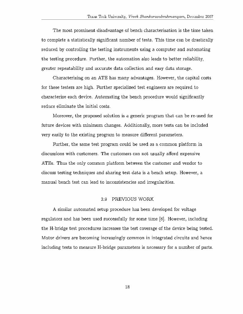
3.1 TEST SYSTEM OVERVIEW
The proposed solution looks at automating the test procedure by controlling
the instruments and the devices with a computer. As shown in Figure 3.1, the test
system consists of the device under test (DUT), a device speci�c evaluation board,
the instruments needed to test the IC and a computer to control the instruments.
The DUT is placed on a device-speci�c evaluation board. This evaluation
board is then connected to the various instruments. A computer is used to control
the instruments and sometimes even the device. The instruments are programmed
using Standard Commands for Programming Instrumentation (SCPI), an
instrumentation language.
Figure 3.1: Test system overview
19

Texas Tech University, Vivek Shankarasubrahmanyam, December 2007
3.1.1 Instrument Set
The instrument set typically consists of source-meters, multi-meters,
oscilloscopes etc. The most common instrument sets consist of Keithley
source-meters: K2430 and K2602; Agilent multi-meter: AG34401; a Tektronix
digital oscilloscope: DPO7054; and a decade resistance box. These instruments
are su�cient for most applications.
3.1.1.1 Keithley 2602 (K2602)
The Keithley 2602 is a dual channel source-meter that can act as either a
current or a voltage source. It combines a precision power supply, true current
source and DMM. It can be con�gured as two independent isolated sources for
voltage or current. The voltage source can range from 5 uV to 40 V, while the
current source can range from 5 pA to 3 A. The meter can measure as low as 1 uV
and 1 pA. It is possible to measure current and voltage simultaneously on each
channel at very high speeds.
The instrument has separate oversized locking screw terminal connections for
each channel. Connections are provided for OUTPUT HI and LO, SENSE HI and
LO, and GUARD. Banana triax adapter cables are available for wiring exibility
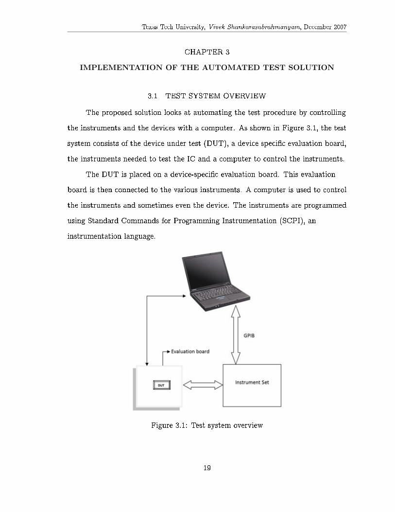
[15]. A brief overview of the meter speci�cations is shown in Table 3.1 [15].
3.1.1.2 Keithley 2430
The Keithley 2430 is also a source meter, similar to the K2602. However,
unlike the K2602, it has only one output channel. For the tests done in this work,
the K2430 and K2602 are interchangeable. However, the K2430 has the additional
capability of producing voltage pulses with durations as small as 50 ms [8]. The
inclusion of the K2430 gives the test engineer / technician an extra option while
choosing instruments.
20
Texas Tech University, Vivek Shankarasubrahmanyam, December 2007
Table 3.1: Condensed speci�cations of Keithley 2602
The K2430 is easy to set up and use. It provides convenient DMM-like
operation. It allows sourcing voltage or current while making measurements,
without changing connections. It is IEEE-488.2 compatible for instrument control.
LabVIEW and TestPoint drivers are available [16]. The programming ranges of
the K2430 are shown in table 3.2 [16]. The measurement accuracy of the K2430 is
shown in the table 3.3 [16].
3.1.1.3 Agilent 34401
The Agilent 34401 is a 612digit, high performance digital multi-meter that
has GPIB capability. The multi-meter will be connected across the FETs to
measure the voltage drop. Additional meters help in evaluating the voltage drops
across di�erent FETs simultaneously [17]. The ranges of the AG34401 are shown
in the table 3.4 [17].
21

Texas Tech University, Vivek Shankarasubrahmanyam, December 2007
Table 3.2: Keithley 2430 voltage and current programming accuracy
3.1.1.4 Tektronix DPO7054
The DPO7054 is a Tektronix digital oscilloscope. It has four inputs, but
only one is required in this application. Channel 1 can be used to measure the rise
and fall time of the output voltage, measured across the load. A decade resistance
box can be used as the load. The scope has a 500 MHz bandwidth and a
maximum sampling rate of 10 GS/s [18]. It has the capability to store the
waveform image and also to export the waveform data out the GPIB port.
22

Texas Tech University, Vivek Shankarasubrahmanyam, December 2007
Table 3.3: Measurement accuracy of Keithley 2430
Table 3.4: Agilent DMM - DC Voltage measurement accuracy
3.1.1.5 GPIB
The instruments are connected to the computer through GPIB connectors
[19]. GPIB stands for General Purpose Interface Bus. The interface is versatile
and can be used to control most instruments. It consists of 16 signal lines: 8 data
lines, 3 handshake lines and 5 interface management lines.
The GPIB standard greatly simpli�es the interconnection of programmable
23
Texas Tech University, Vivek Shankarasubrahmanyam, December 2007
instruments by clearly de�ning mechanical, hardware, and electrical protocol
speci�cations. Further, instruments from di�erent manufactures can be connected
by a standard cable. Connecting instruments from di�erent manufacturers is
almost always necessary while testing.
3.2 SOFTWARE CONTROL
The control software was designed and coded in LabVIEW. There are two
di�erent modules: DC and AC. The DC module performs DC parametric tests.
The AC module performs rise time and fall time measurements. The AC module
is separated so that future AC tests can be coded separately from the DC module.
3.2.1 Introduction to LabVIEW
The human mind can understand complex inter-relations more easily when
they are represented pictographically. It is customary for a programmer to draw
ow charts, structure diagrams, Petri nets to aid to specify algorithms, data
structures and other inter-dependencies. This principle led to the introduction of
a programming system based on a data ow model extended with graphical
control- ow structures: the LabVIEW development environment with its
embedded G programming language. The development of LabVIEW was
in uenced by laboratory automation. LabVIEW is employed in a wide variety of
industries, such as automated testing, industrial automation, laboratory
automation, automotive engineering, personal instrumentation, etc., to build
virtual instrumentation systems.
LabVIEW programs are essentially a hierarchy of instrument-like modules,
called virtual instruments (VIs). The VIs are composed of user interfaces (front
panels) with visual programming (block diagrams). This blend of development
24
Texas Tech University, Vivek Shankarasubrahmanyam, December 2007
and execution can be considered as a major advantage of LabVIEW's graphical
programming environment. The other advantages of LabVIEW are: ease of use,
natural representation, rapid proto-typing, code reusability, etc.
LabVIEW programming consists of placing objects on the block diagram
and wiring them. Thus, the program consists of blocks that are wired to represent
the data ow. It allows the development of the user front-end concurrently
without any additionally programming. The controls and indicators used in the
front-end have associated graphics that is used to represent them in the front-end.
Each LabVIEW program consists of three panes: a block diagram, a front
panel and a connector pane. Controls and indicators are placed on the front panel
and form the user-interface for the operator to input data or view output.
Further, each VI can be run as an individual program or included as a part of
another larger program. The VIs can be treated as functions in typical text-based
programming language. Thus, individual VIs can be tested before being included
as a part of larger programs [8, 9].
3.3 DC MODULE
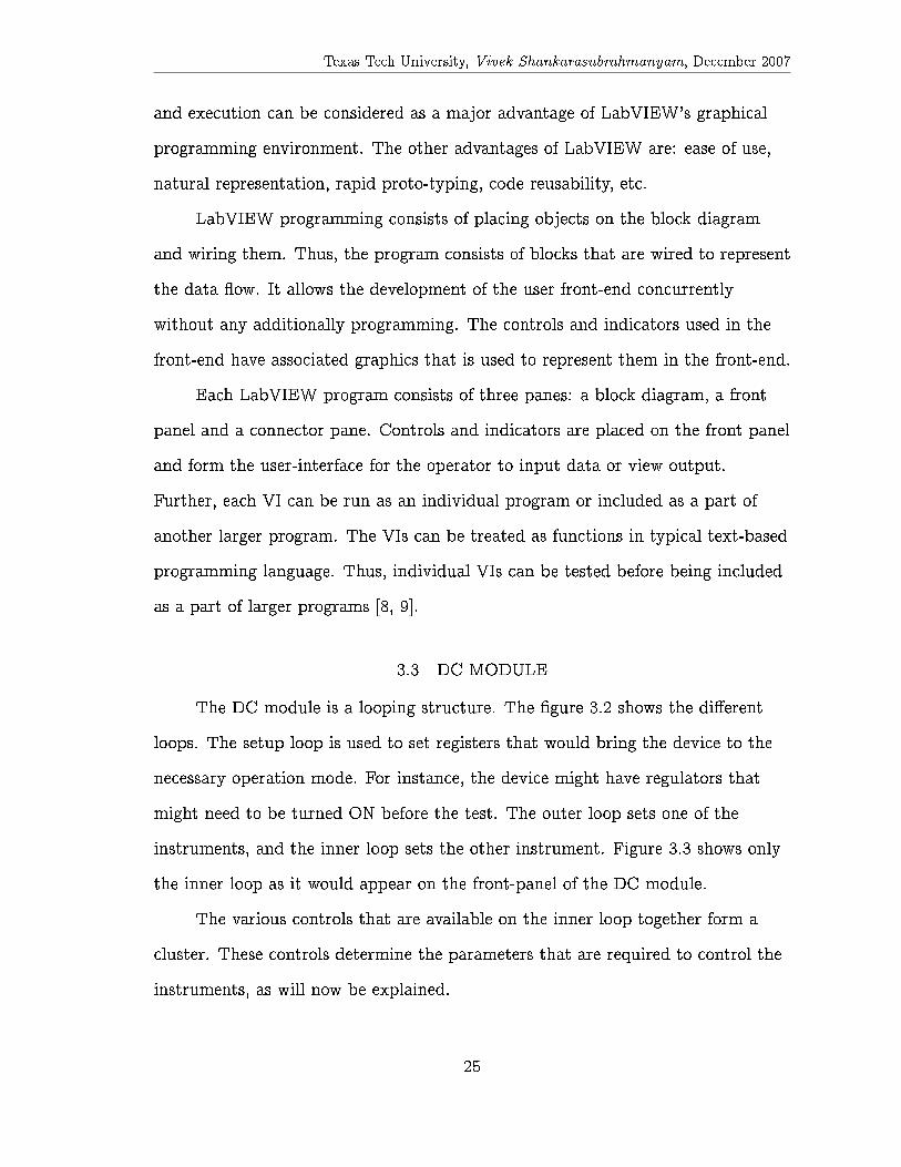
The DC module is a looping structure. The �gure 3.2 shows the di�erent
loops. The setup loop is used to set registers that would bring the device to the
necessary operation mode. For instance, the device might have regulators that
might need to be turned ON before the test. The outer loop sets one of the
instruments, and the inner loop sets the other instrument. Figure 3.3 shows only
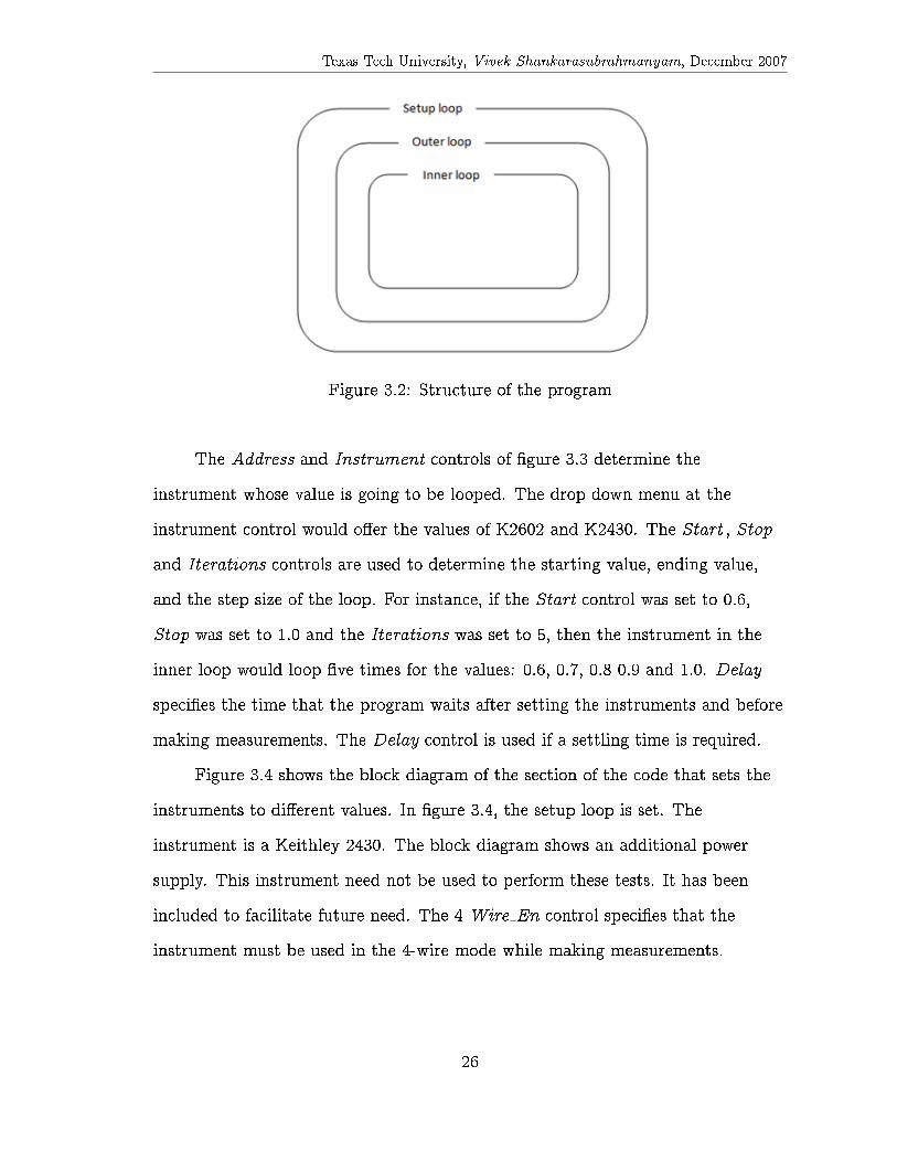
the inner loop as it would appear on the front-panel of the DC module.
The various controls that are available on the inner loop together form a
cluster. These controls determine the parameters that are required to control the
instruments, as will now be explained.
25
Texas Tech University, Vivek Shankarasubrahmanyam, December 2007
Figure 3.2: Structure of the program
The Address and Instrument controls of �gure 3.3 determine the
instrument whose value is going to be looped. The drop down menu at the
instrument control would o�er the values of K2602 and K2430. The Start , Stop
and Iterations controls are used to determine the starting value, ending value,
and the step size of the loop. For instance, if the Start control was set to 0.6,
Stop was set to 1.0 and the Iterations was set to 5, then the instrument in the
inner loop would loop �ve times for the values: 0.6, 0.7, 0.8 0.9 and 1.0. Delay
speci�es the time that the program waits after setting the instruments and before
making measurements. The Delay control is used if a settling time is required.
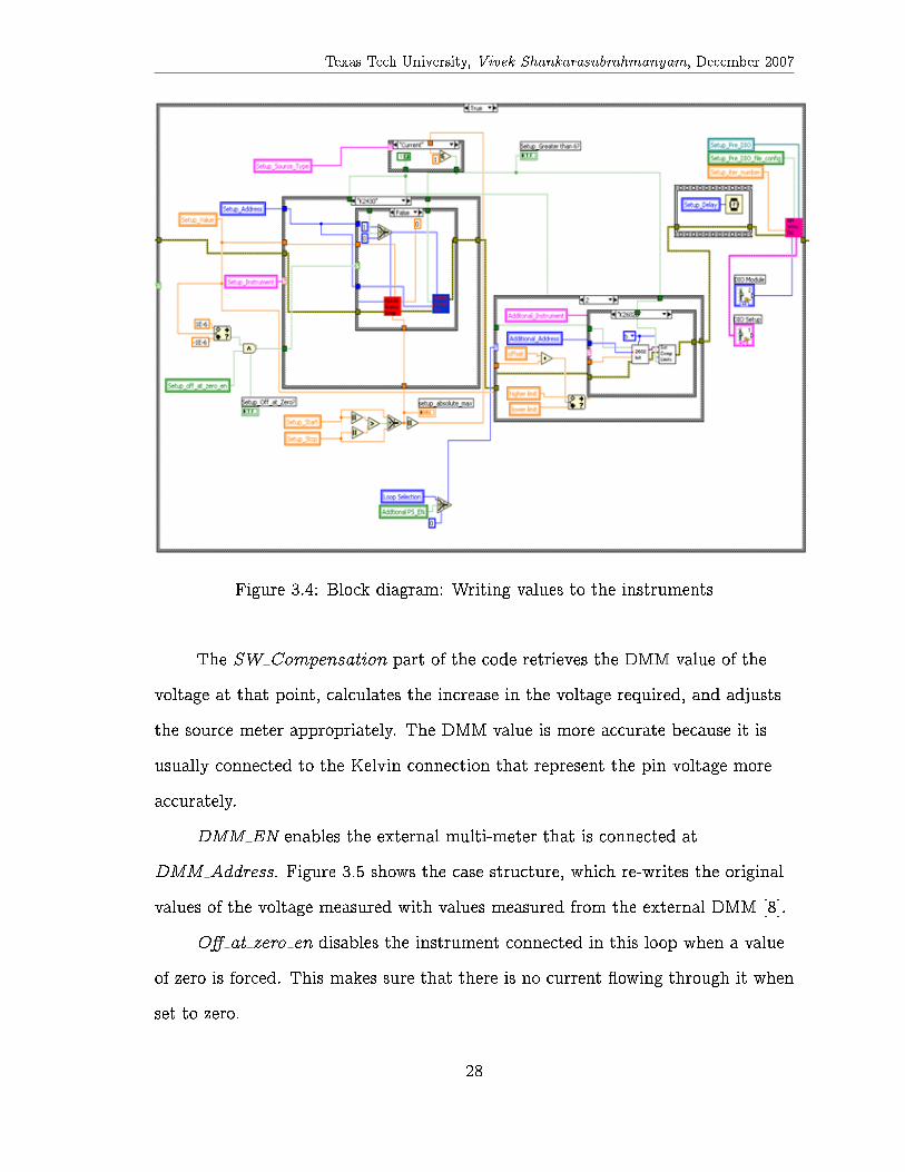
Figure 3.4 shows the block diagram of the section of the code that sets the
instruments to di�erent values. In �gure 3.4, the setup loop is set. The
instrument is a Keithley 2430. The block diagram shows an additional power
supply. This instrument need not be used to perform these tests. It has been
included to facilitate future need. The 4 Wire En control speci�es that the
instrument must be used in the 4-wire mode while making measurements.
26
Texas Tech University, Vivek Shankarasubrahmanyam, December 2007
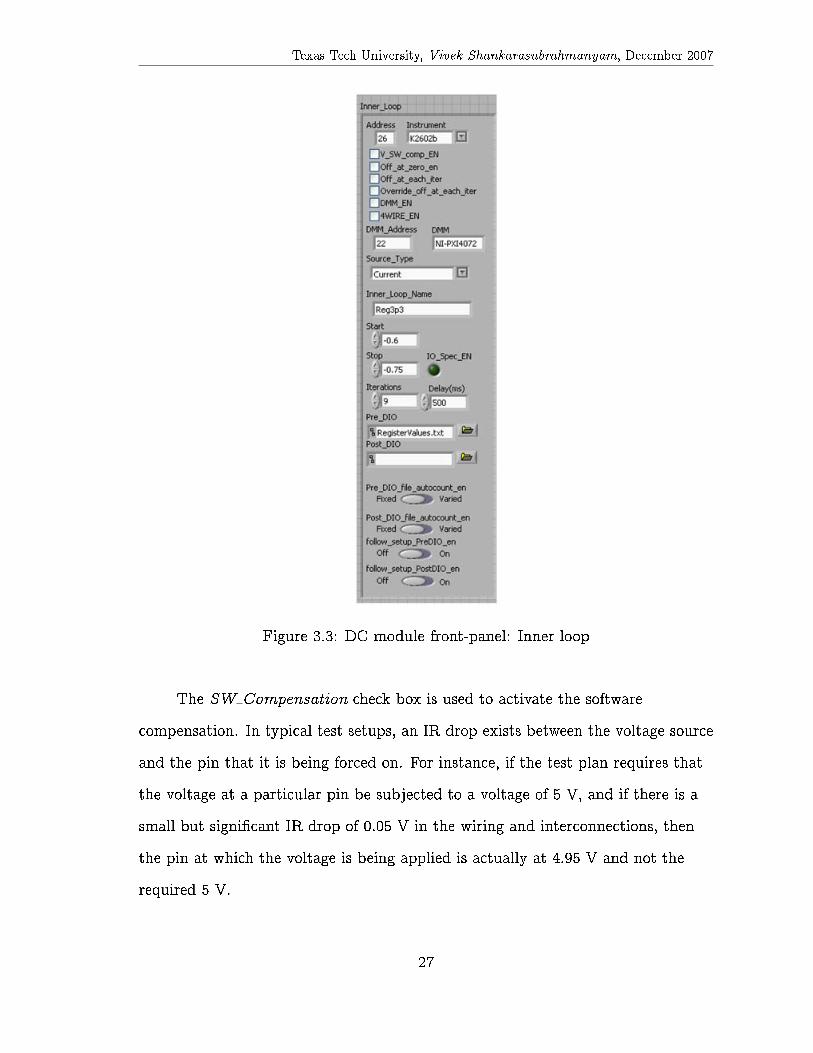
Figure 3.3: DC module front-panel: Inner loop
The SW Compensation check box is used to activate the software
compensation. In typical test setups, an IR drop exists between the voltage source
and the pin that it is being forced on. For instance, if the test plan requires that
the voltage at a particular pin be subjected to a voltage of 5 V, and if there is a
small but signi�cant IR drop of 0.05 V in the wiring and interconnections, then
the pin at which the voltage is being applied is actually at 4.95 V and not the
required 5 V.
27
Texas Tech University, Vivek Shankarasubrahmanyam, December 2007
Figure 3.4: Block diagram: Writing values to the instruments
The SW Compensation part of the code retrieves the DMM value of the
voltage at that point, calculates the increase in the voltage required, and adjusts
the source meter appropriately. The DMM value is more accurate because it is
usually connected to the Kelvin connection that represent the pin voltage more
accurately.
DMM EN enables the external multi-meter that is connected at
DMM Address. Figure 3.5 shows the case structure, which re-writes the original
values of the voltage measured with values measured from the external DMM [8].
O� at zero en disables the instrument connected in this loop when a value
of zero is forced. This makes sure that there is no current owing through it when
set to zero.
28

Texas Tech University, Vivek Shankarasubrahmanyam, December 2007
Figure 3.5: Block diagram: Enabling external DMM
O� at each iter switches the instrument OFF between successive iterations.
Thus, if the instrument steps from 0.6 A to 0.7 A, it would �rst turn o� and then
switch to 0.7A.
The device often must be set into di�erent operating modes before or after
conducting the test. For instance, certain register values might be altered to turn
a regulator ON or OFF after the test has been completed.
These operations are done through a serial peripheral interface (SPI)
communication port of the DUT. Pre DIO and Post DIO are paths to the �les to
be executed before and after the loop has been executed, respectively. This is
performed using an external executable �le that LabVIEW calls. The slide
switches Pre DIO �le autocount en and Post DIO �le autocount en enable
automatic selection of di�erent �les during successive iterations. The �le names
29

Texas Tech University, Vivek Shankarasubrahmanyam, December 2007
must be sequentially named. The code automatically chooses the next �le based
on the �le name. The �les must be named in the �lename iter.txt format where
the "iter" speci�es the iteration value. For example, the �le names could be
sample 1.txt, sample 2.txt, sample 3.txt etc. The �gure 3.6 shows the part of the
code that determines the new �le name.
Figure 3.6: Block diagram: Creating new �le names
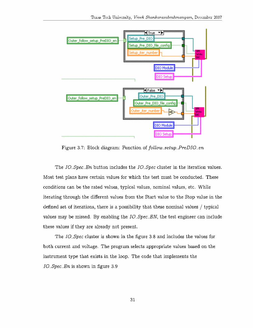
The slide switches follow setup PreDIO en and follow setup PostDIO en
ensure that the device is put under the same condition each iteration. This is
required in case the device gets reset during the test. Figure 3.7 shows the
conditional structure that would be executed if these slide switches are enabled.
The Inner Loop Name could be used by the test engineer to distinguish
between the di�erent loops in the output �le. The same looping structure exists
for the outer loop and the setup loop. The setup loop does not have an option to
include a setup loop name. This is not a major disadvantage because the setup
loop is generally used only to set certain register values.
30
Texas Tech University, Vivek Shankarasubrahmanyam, December 2007
Figure 3.7: Block diagram: Function of follow setup PreDIO en
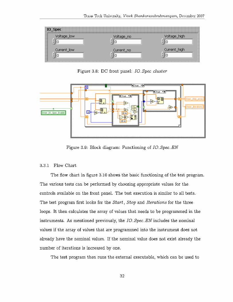
The IO Spec En button includes the IO Spec cluster in the iteration values.
Most test plans have certain values for which the test must be conducted. These
conditions can be the rated values, typical values, nominal values, etc. While
iterating through the di�erent values from the Start value to the Stop value in the
de�ned set of iterations, there is a possibility that these nominal values / typical
values may be missed. By enabling the IO Spec EN, the test engineer can include
these values if they are already not present.
The IO Spec cluster is shown in the �gure 3.8 and includes the values for
both current and voltage. The program selects appropriate values based on the
instrument type that exists in the loop. The code that implements the
IO Spec En is shown in �gure 3.9
31
Texas Tech University, Vivek Shankarasubrahmanyam, December 2007
Figure 3.8: DC front panel: IO Spec cluster
Figure 3.9: Block diagram: Functioning of IO Spec EN
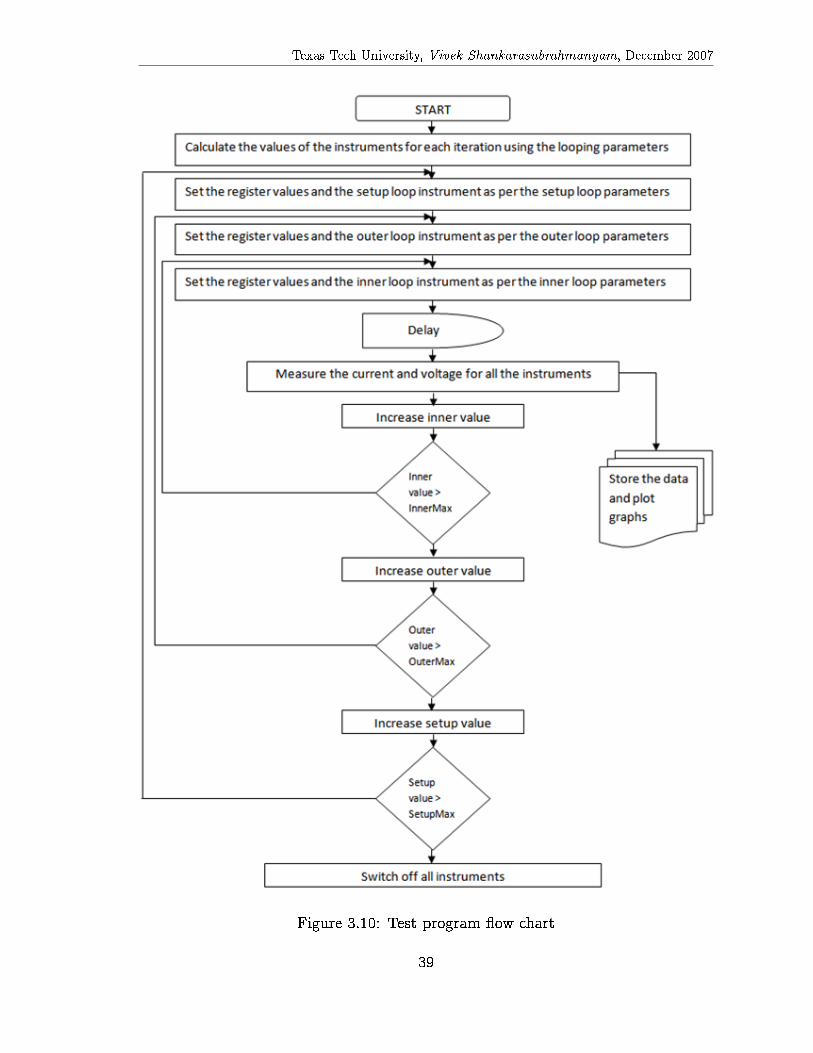
3.3.1 Flow Chart
The ow chart in �gure 3.10 shows the basic functioning of the test program.
The various tests can be performed by choosing appropriate values for the
controls available on the front panel. The test execution is similar to all tests.
The test program �rst looks for the Start , Stop and Iterations for the three
loops. It then calculates the array of values that needs to be programmed in the
instruments. As mentioned previously, the IO Spec EN includes the nominal
values if the array of values that are programmed into the instrument does not
already have the nominal values. If the nominal value does not exist already the
number of iterations is increased by one.
The test program then runs the external executable, which can be used to
32

Texas Tech University, Vivek Shankarasubrahmanyam, December 2007
control the state of the device. Often, the device's internal register value must be
altered to bring the device to an operational mode to be tested.
This is achieved through an external executable that LabVIEW calls. After
bringing the device into the desired operational mode, the setup instruments are
initialized. The values depend on the Start , Stop and Iterations control
variables. After completing the setup loop portion of the code, the test program
proceeds to the outer loop. The functioning of this part of the code is similar to
that of the setup loop portion of the code. After completing the outer loop, the
test program enters the inner loop. After setting all instruments that have been
speci�ed in the front panel, the test program proceeds to the section of the code
that makes the measurements. The voltage values measured by the source-meter
can be replaced by more precise DMM measurements if appropriate controls are
chosen in the front panel. Calculations are then made from these values to
evaluate the parameters that are being tested. For instance, Rds(ON) .
After the measurements and calculations, the output �les can be written in a
comma separated value (csv) format. The option for the output �le must be
selected on the front panel. Figure 3.11 shows the section of the front panel where
the user can select whether to write a new �le or to append to an existing �le.
The output �le has many columns that include information about the DUT, the
test performed, the date and the time.
The test program then proceeds to the next iteration of the inner loop and
subsequently the outer and setup loops. Much of the testing can be performed
using two loops. However, the presence of three loops gives exibility to the
future tests and devices.
An additional power supply can optionally be included. This additional
power supply is a very useful feature for devices that require more power supplies.
33

Texas Tech University, Vivek Shankarasubrahmanyam, December 2007
The power supplies could be either the Keithley 2602 or 2430. The additional
power supply can be included in any of the loops. The additional power supply
can trace any of the other loops.
The DC module has the capability of producing and saving graphs from the
data collected. The graphs change with the test con�guration selected. The graph
can then be saved in JPEG, BMP or PNG format, with varying depths of the
image for image quality. The graphs are plotted for di�erent values of the result,
depending on the test con�guration. The graph plots, by default, the value of the
result of the test on the y-axis and the inner loop parameter on the x-axis.
Multiple lines are drawn for each setup loop iteration and outer loop iteration.
The user also has an option of plotting only the last value of the result with the
outer loop as the x-axis. The di�erent lines correspond to the di�erent setup loop
iterations. This helps in graphing the extreme condition for various setup
conditions. The Inner loop abort cluster allows the engineer to test the extreme
limits of the device. This cluster modi�es the looping structure such that, if the
measured value of the source variable does not satisfy the Condition set by
Number1 and Number2, then the inner loop will end, and the program will go on
to the next outer loop iteration. Setting this condition allows the engineer to test
the limits of a device when the actual limits are not known.
The con�guration drop down box lists the tests that can be performed. It
includes Rds(ON) , Vfb , Vdrop and leakage. The portion of the front panel shown in
�gure 3.12 deals with the running of the program. The buttons START and
STOP control the execution of the program. If STOP is pressed, the test
execution comes to a stop at the end of the current iteration. If ABORT is
pressed, the execution is stopped immediately [8].
34

Texas Tech University, Vivek Shankarasubrahmanyam, December 2007
3.3.2 Test Con�gurations
The test con�guration can be used to de�ne default values for the
instruments to be connected in various loops. The user has the option of changing
the default value and also choosing the Start, Stop and Iteration controls based on
the characterization plan.
Rds(ON) :
In the Rds(ON) test, current must be forced through the conducting FET, and the
voltage drop across the FET is measured. The default value for the inner loop is
the Keithley 2430 as a current source, and the outer loop has the Keithley 2602 as
a voltage source. The K2602 is used as the voltage supply for the H-bridge. The
measurement of the voltage requires two DMMs. One DMM is connected to the
drain of the FET, and the other is connected to the FET's source. The Rds(ON)
value can then be calculated from equation 3.1:
Rds(ON) =(Vout−Vin)
Iin
(3.1)
where
Vout is the voltage measured at the drain,
Vin is the voltage measured at the source, and
Iin is the current owing through the FET.
The measurement part of the code is shown in �gure 3.13
Vfb :
The forward body diode voltage drop requires only one loop. The default
instrument for the inner loop is the Keithley 2430, which acts as a current source.
35
Texas Tech University, Vivek Shankarasubrahmanyam, December 2007
The voltage drop can be measured by the instrument itself or by an external
DMM. The voltage drop between the drain and the source is the forward body
diode voltage.
Leakage:
The default instruments for the leakage measurements are similar to those of the
Rds(ON) test. The voltage is forced at the H-bridge supply. The current leaking
through the FET is measured in the inner loop with the Keithley 2430. The
leakage current is on the order of nano-amperes. The K2430 has su�cient
accuracy to measure current at this level. The voltage of the K2430 is set to 0 to
simulate a GND connection.
Vdrop :
The default instruments for the Vdrop test are the same as that of Rds(ON) ,
because the test is very similar to it. The voltage drop across the FETs is
data-logged in this case. For some devices, the Vdrop speci�cation is given as the
sum of the voltage drop across both FETs in either path. In such a case, a minor
change in the code is required to compute the Vdrop . Two external DMMs are
required to measure the voltage drop across each FET, and the sum of these
voltage drops can be data-logged.
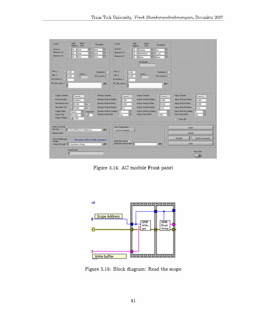
3.4 AC MODULE
The AC Module is similar in structure to its DC counterpart. The AC
Module consists of two loops instead of the three loops in the DC module. The
loops iterate through speci�ed inputs and device settings. The outer loop can be
used to write di�erent register settings to the IC, and the inner loop loops through
the instrument settings. Each loop has a source and two measurements that can
be made. The Parameter drop down box tells the program the type of source and
36

Texas Tech University, Vivek Shankarasubrahmanyam, December 2007
type of measurement that is being made, and that parameter gets written to the
output .csv �le. The Feedback checkbox is the same as the 4WIRE EN in the DC
Module and allows 4-wire measurement of voltage signals. SPI Control allows the
use of the SPI write commands to set register values inside of the PMIC [8].
All the setting options of the oscilloscope are included for remote control
through the front panel. For the rise time and fall time measurements, only one
channel is required. However, additional capability is included for future tests.
The user can control any of the options on the control panel. The AC module
yields a graph similar to the DC module. The rise time and fall time
measurements are plotted for di�erent voltage values. The supply to the H-bridges
can be varied by connecting the Keithley 2430 to the inner loop and using it as a
voltage source. A resistive load should be included across the H-bridge outputs.
The voltage across the load should be fed to the oscilloscope. The oscilloscope can
measure the rise time and fall time of the waveform. The waveform being
captured is de�ned by the options that are chosen on the front panel.
The oscilloscope always measures the rise time and fall time of the waveform.
The test program writes a SCPI command to retrieve information about the rise
time and fall time from the oscilloscope. Figure 3.14 shows the front panel of the
AC module. The rise and fall time measurements are not the only important AC
parameters. This module could be developed further to measure analog and digital
current limit, operational frequency, over current shutdown, etc. The rise and fall
time measurements are only implemented to show the gain of such a system.
The GPIB Write module which writes the commands to the instrument is
shown in the �gure 3.15.
The block GPIB Write gen shown in the �gure 3.15 writes the instructions
to the scope through the GPIB. The write bu�er is a SCPI command which
37

Texas Tech University, Vivek Shankarasubrahmanyam, December 2007
instructs the scope to return the value of the rise time and fall time. Figure 3.16
shows the block diagram of the GPIB Write gen block.
The block diagram in �gure 3.16 writes the contents of the write bu�er to
the instrument connected at the address speci�ed in the GPIB Address. Then
the instrument is read in the block GPIB Read String. The scope returns the
rise time and fall time based on the Write bu�er. The output is written to a
Output Bu�er. The rise and fall time is then appropriately indexed to the output
using an index array block shown in the �gure 3.17. The rise or fall time is then
written to an output �le.
3.5 SUMMARY
The DC and AC module has been developed with generality in mind. The
program is exible to include additional tests as needed. Further, the availability
of additional loops in the DC module would facilitate testing devices which need
elaborate procedures to turn ON. The program includes functionality to include
additional power supplies, write graphs, etc.
38
Texas Tech University, Vivek Shankarasubrahmanyam, December 2007
Figure 3.10: Test program ow chart
39
Texas Tech University, Vivek Shankarasubrahmanyam, December 2007
Figure 3.11: DC module front panel: Output �le
Figure 3.12: DC module front panel: Execution control
Figure 3.13: Block Diagram: Calculating Rds(ON)
40
Texas Tech University, Vivek Shankarasubrahmanyam, December 2007
Figure 3.14: AC module Front panel
Figure 3.15: Block diagram: Read the scope
41

Texas Tech University, Vivek Shankarasubrahmanyam, December 2007
Figure 3.16: Block diagram: GPIB Write
Figure 3.17: Block diagram: Index array block retrieving rise time from the output
bu�er
42

Texas Tech University, Vivek Shankarasubrahmanyam, December 2007
CHAPTER 4
DATA AND COST ANALYSIS
The following chapter discusses the test results accumulated from the
program described in chapter 3. Further, a cost analysis is included to give the
reader a perspective the e�ciency of this characterization solution.
4.1 TEST RESULTS
The tests results from multiple devices are considered. The test results of a
sample of around 30 devices are analyzed. Furthermore, the test results from the
same device tested 30 times are also analyzed. The device that is tested consists
of 6 di�erent H-bridges. Only one H-bridge is tested to prove that the test
program is functioning and that the data accumulated is reliable. Before,
analyzing the results it is helpful to review a parameter that gives an indication of
the test repeatability.
Capability index (Cpk):
It is not an unusual practice to assume a set of measurements made on any IC to
constitute a normal distribution. This assumption aids in analyzing the process
capability index which is de�ned by equation 4.1.
Cpk = minf (µ−LSL)3σ
, (USL−µ)3σ
g
(4.1)
where
Cpk is the capability index,
µ is the mean,
43

Texas Tech University, Vivek Shankarasubrahmanyam, December 2007
σ is the standard deviation,
LSL is the lower spec limit, and
USL is the upper spec limit.
The Cpk value gives a measure of the percentage of the values that would
fall within the speci�cation limits. Thus, this percentage is based on the mean,
standard deviation of the sample and the speci�cation limits. Since the
distribution is assumed to normal, the distribution curve is symmetrical about the
mean. The probability of the measurement to fall in the interval running one
standard deviation on either direction of the mean is 0.683. Similar probabilities
for intervals running two and three standard deviations on either direction of the
mean are 0.954 and 0.997. Hence, if in any distribution, the speci�cation limits
are 3 standard deviations from the mean in any direction, it is fairly reasonable to
expect the measurement to be within the speci�cation limits 99.7% of the times.
Thus a higher Cpk indicates that the test is repeatable. In the semiconductor
industry, a Cpk greater than 2 is considered acceptable in many cases [20].
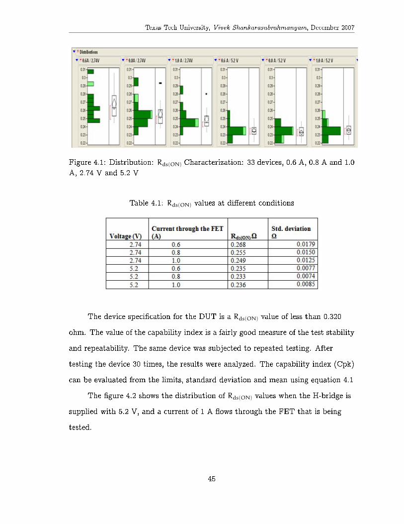
4.1.1 Rds(ON)
The test results for Rds(ON) from 33 devices tested consecutively are
analyzed. Figure 4.1 shows the histogram of the distributions. The Rds(ON)
measurements at three di�erent currents and two di�erent voltages are analyzed.
The test results for Rds(ON) with the FET sourcing 0.6 A, 0.8 A and 1.0 A
are shown in �gure 4.1. The �gure also shows the Rds(ON) values at the
aforementioned currents while the H-bridge is supplied by two di�erent voltages:
2.74 V and 5.2 V. Table 4.1 shows the various values of mean and standard
deviation of the Rds(ON) values at di�erent conditions.
44
Texas Tech University, Vivek Shankarasubrahmanyam, December 2007
Figure 4.1: Distribution: Rds(ON) Characterization: 33 devices, 0.6 A, 0.8 A and 1.0
A, 2.74 V and 5.2 V
Table 4.1: Rds(ON) values at di�erent conditions
The device speci�cation for the DUT is a Rds(ON) value of less than 0.320
ohm. The value of the capability index is a fairly good measure of the test stability
and repeatability. The same device was subjected to repeated testing. After
testing the device 30 times, the results were analyzed. The capability index (Cpk)
can be evaluated from the limits, standard deviation and mean using equation 4.1
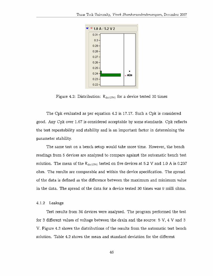
The �gure 4.2 shows the distribution of Rds(ON) values when the H-bridge is
supplied with 5.2 V, and a current of 1 A ows through the FET that is being
tested.
45
Texas Tech University, Vivek Shankarasubrahmanyam, December 2007
Figure 4.2: Distribution: Rds(ON) for a device tested 30 times
The Cpk evaluated as per equation 4.2 is 17.17. Such a Cpk is considered
good. Any Cpk over 1.67 is considered acceptable by some standards. Cpk re ects
the test repeatability and stability and is an important factor in determining the
parameter stability.
The same test on a bench setup would take more time. However, the bench
readings from 5 devices are analyzed to compare against the automatic bench test
solution. The mean of the Rds(ON) tested on �ve devices at 5.2 V and 1.0 A is 0.237
ohm. The results are comparable and within the device speci�cation. The spread
of the data is de�ned as the di�erence between the maximum and minimum value
in the data. The spread of the data for a device tested 30 times was 9 milli ohms.
4.1.2 Leakage
Test results from 34 devices were analyzed. The program performed the test
for 3 di�erent values of voltage between the drain and the source: 5 V, 4 V and 3
V. Figure 4.3 shows the distributions of the results from the automatic test bench
solution. Table 4.2 shows the mean and standard deviation for the di�erent
46
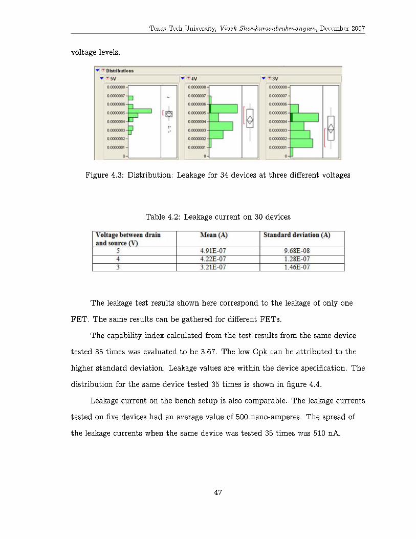
Texas Tech University, Vivek Shankarasubrahmanyam, December 2007
voltage levels.
Figure 4.3: Distribution: Leakage for 34 devices at three di�erent voltages
Table 4.2: Leakage current on 30 devices
The leakage test results shown here correspond to the leakage of only one
FET. The same results can be gathered for di�erent FETs.
The capability index calculated from the test results from the same device
tested 35 times was evaluated to be 3.67. The low Cpk can be attributed to the
higher standard deviation. Leakage values are within the device speci�cation. The
distribution for the same device tested 35 times is shown in �gure 4.4.
Leakage current on the bench setup is also comparable. The leakage currents
tested on �ve devices had an average value of 500 nano-amperes. The spread of
the leakage currents when the same device was tested 35 times was 510 nA.
47
Texas Tech University, Vivek Shankarasubrahmanyam, December 2007
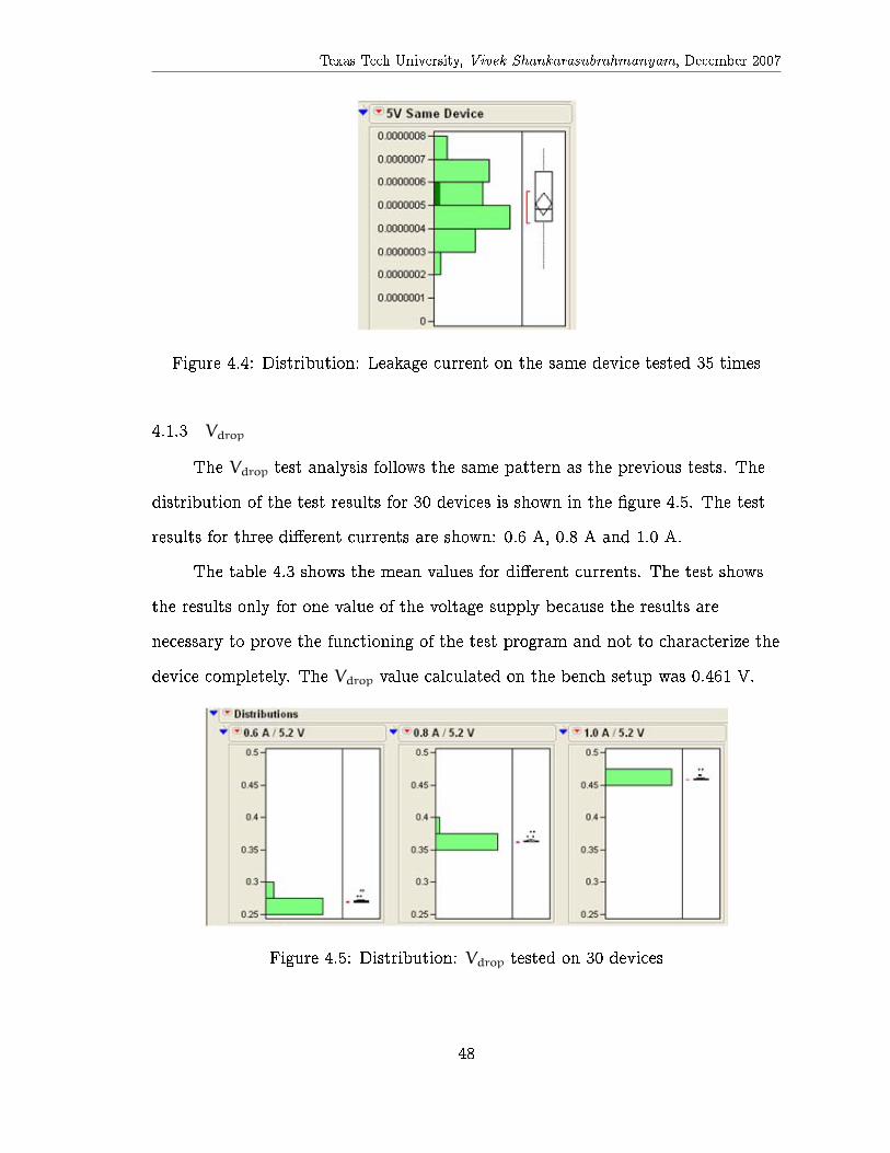
Figure 4.4: Distribution: Leakage current on the same device tested 35 times
4.1.3 Vdrop
The Vdrop test analysis follows the same pattern as the previous tests. The
distribution of the test results for 30 devices is shown in the �gure 4.5. The test
results for three di�erent currents are shown: 0.6 A, 0.8 A and 1.0 A.
The table 4.3 shows the mean values for di�erent currents. The test shows
the results only for one value of the voltage supply because the results are
necessary to prove the functioning of the test program and not to characterize the
device completely. The Vdrop value calculated on the bench setup was 0.461 V.
Figure 4.5: Distribution: Vdrop tested on 30 devices
48

Texas Tech University, Vivek Shankarasubrahmanyam, December 2007
Table 4.3: Vdrop test for 30 devices
The Cpk calculated as per equation 4.1 for the results accumulated from
testing the same device multiple times is 3.9. The device speci�cation is 0.64. The
�gure 4.6 shows the distribution of the test results for the same device tested 30
times. The spread of the data when the same device was tested 30 times was 13
mV.
Figure 4.6: Distribution: Vdrop values of the same device tested 30 times
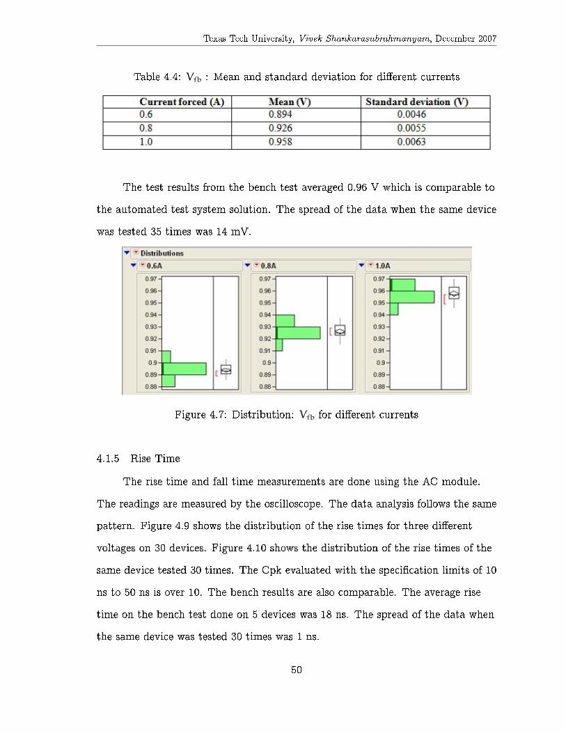
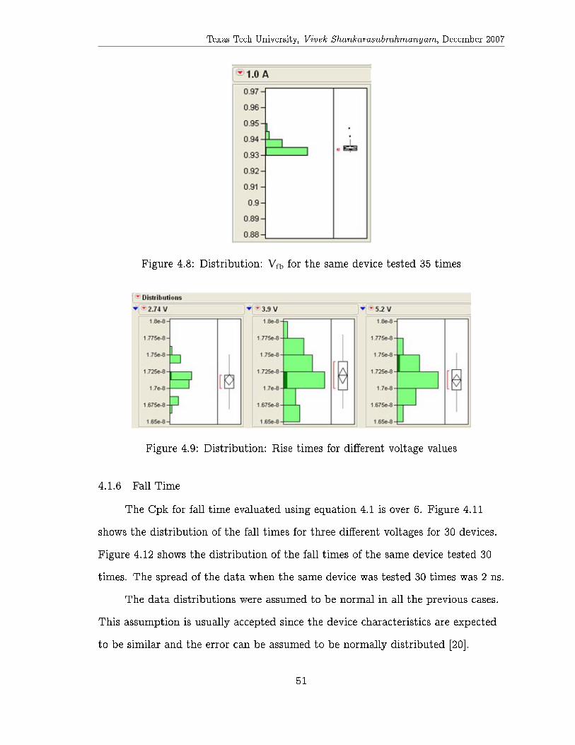
4.1.4 Vfb
The distributions of the test results for three di�erent currents for 30 devices
are shown in �gure 4.7. The means and standard deviations are tabulated in table
4.4. The distribution of the test results when the same device is tested 35 times is
shown in �gure 4.8. The Cpk evaluated with speci�cation limits as 1.5V is over 10.
49
Texas Tech University, Vivek Shankarasubrahmanyam, December 2007
Table 4.4: Vfb : Mean and standard deviation for di�erent currents
The test results from the bench test averaged 0.96 V which is comparable to
the automated test system solution. The spread of the data when the same device
was tested 35 times was 14 mV.
Figure 4.7: Distribution: Vfb for di�erent currents
4.1.5 Rise Time
The rise time and fall time measurements are done using the AC module.
The readings are measured by the oscilloscope. The data analysis follows the same
pattern. Figure 4.9 shows the distribution of the rise times for three di�erent
voltages on 30 devices. Figure 4.10 shows the distribution of the rise times of the
same device tested 30 times. The Cpk evaluated with the speci�cation limits of 10
ns to 50 ns is over 10. The bench results are also comparable. The average rise
time on the bench test done on 5 devices was 18 ns. The spread of the data when
the same device was tested 30 times was 1 ns.
50
Texas Tech University, Vivek Shankarasubrahmanyam, December 2007
Figure 4.8: Distribution: Vfb for the same device tested 35 times
Figure 4.9: Distribution: Rise times for di�erent voltage values
4.1.6 Fall Time
The Cpk for fall time evaluated using equation 4.1 is over 6. Figure 4.11
shows the distribution of the fall times for three di�erent voltages for 30 devices.
Figure 4.12 shows the distribution of the fall times of the same device tested 30
times. The spread of the data when the same device was tested 30 times was 2 ns.
The data distributions were assumed to be normal in all the previous cases.
This assumption is usually accepted since the device characteristics are expected
to be similar and the error can be assumed to be normally distributed [20].
51

Texas Tech University, Vivek Shankarasubrahmanyam, December 2007
Figure 4.10: Distribution: Rise times for the same device tested 30 times
Figure 4.11: Distribution: Fall times for di�erent voltage values
4.2 COST ANALYSIS
4.2.1 Test Time
The automated bench setup is faster than bench testing but not as fast as
the ATE. The idea behind developing an automated bench setup is to create a
balance between the cost of bench testing and speed of the ATE. The testing
speed on a bench varies from person to person and is di�erent for the same person
at di�erent times. Thus, the exact test time on the bench cannot be really
measured. However, a reasonable approximation is possible.
52

Texas Tech University, Vivek Shankarasubrahmanyam, December 2007
Figure 4.12: Distribution: Fall times for same device test 30 times
The average time taken to test for Rds(ON) on the bench could be
approximated as 90 seconds for one measurement. This is fairly optimistic
considering the fact that the technician must log the data between successive
measurements. The automated setup can measure a value in less than 3 seconds.
This estimate is pessimistic but has been assumed for the worst case analysis. If a
device characterization involves 1000 measurements, the automated setup would
complete the test in an hour, whereas bench testing would take up to 25 hours.
Testing on the bench for one parameter voer 25 hours would be infeasible.
Further, the technician must be at the bench during the entire test. In the
case of an automated test setup, the technician must setup the instruments and
can concentrate on some other task until test completion.
4.2.2 Test economics
Pro�tability is the di�erence between the revenues generated by a company's
product and the costs associated developing, manufacturing and selling them. Test
53

Texas Tech University, Vivek Shankarasubrahmanyam, December 2007
engineering has a very direct connection to manufacturing costs. As mentioned
previously, testing is a painfully large portion of the total cost of the device.
4.2.2.1 Cost Model
Determining the exact cost of the test is often not possible. However, a test
cost model can be developed by making certain broad assumptions.
Test cost = test cost per second � test time (4.2)
Equation 4.2 is the basic generalization of the test cost. The factor "test
cost per second" has many variables associated with it. They include: tester
depreciation, tester down time, tester idle time, etc. Accurate cost models are
di�cult to develop [7].
4.2.3 Example of test cost
Cost model can be developed with some assumptions. The cost analysis
involves determining the number of devices that will validate the use of an
automated solution. The approximate costs are tabulated in table 4.5.
Table 4.5 shows crude approximations to the real cost, because the various
costs involved would make the analysis confusing. Further, an assumption can be
made that the only costs involved in using a tester are maintenance, labor, and
depreciation of the instruments. Assuming that the power usage, development of
test plan, development of test, the hardware required like the evaluation board
etc. are not the major cost contributors, a cost model can be developed.
Furthermore, from the previous example, the ratio of time taken by each
method is adopted. Hence, a device must be characterized for 25 hours on the
bench, or 50 minutes on the automated bench setup, or 2 minutes on the ATE.
54

Texas Tech University, Vivek Shankarasubrahmanyam, December 2007
Table 4.5: Cost assumptions
Table 4.6 shows the test time for number of devices and the cost associated
in testing in di�erent techniques. The depreciation is assumed to be 20% of the
original value. Maintenance is assumed to be 10% of the original instrument cost.
For the sake of clarity and simplicity, labor is assumed to be a constant on all
platforms, which is however not that accurate. The cost of labor is assumed to be
$30 per hour.
Table 4.6: Test cost for di�erent test techniques
Figures 4.13 and 4.14 show the cost of testing over a number of devices. This
graph can be used to determine the solution that is optimal for the requirements.
55
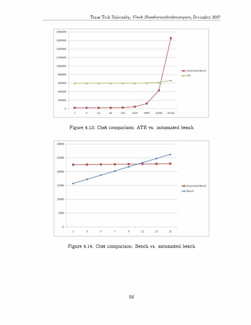
Texas Tech University, Vivek Shankarasubrahmanyam, December 2007
Figure 4.13: Cost comparison: ATE vs. automated bench
Figure 4.14: Cost comparison: Bench vs. automated bench
56
Texas Tech University, Vivek Shankarasubrahmanyam, December 2007
4.3 SUMMARY
The cost analysis shows that automated bench testing forms a viable
solution for characterizing devices. Further, the factor of multiple bench test
equipment required if the number of devices that need to be tested simultaneously
increases has not been considered. Multiple test equipment would add to the cost
in the bench testing and also in the case of automated bench setup if there are a
large number of devices. The cost of ATE is much more reasonable if the number
of devices is greater than 16000 because of the assumption that it takes only 1
hour to characterize a part. The characterization normally takes much more than
1 hour. The analysis considered only the Rds(ON) test. If all the parameters are
considered, the test time would be higher, and the break-even between the ATE
and the automated bench test setup would be much earlier. Moreover, the fact
that multiple units are tested for the same product should be remembered.
57

Texas Tech University, Vivek Shankarasubrahmanyam, December 2007
CHAPTER 5
CONCLUSION
A bench test procedure has many disadvantages as discussed in the second
chapter. An automated bench test setup provides an e�cient alternate that
signi�cantly reduces the test time and hence the cost. The advantages of this
system over bench testing are
1. Less test time
2. Signi�cant reduction in cost of labor
3. Standardization of the testing procedure
4. Standardization of the output format
5. E�cient data logging
6. Better repeatability
7. Ease in sharing test program between the customer and the vendor
Further, the automated bench has certain advantages over the ATE as well.
It is not as expensive. Its accuracy is comparable to that of the ATE. Moreover,
the vendor and customer can share the test program. This sharing is not usually
possible with the ATE programs because the ATEs are expensive for the customer
to buy and maintain.
The automated bench test program is very generic and can be molded to
suit any other test. The program has su�cient instruments to control the device
and make measurements. It is easily extensible. Furthermore, the modular style of
programming lends itself to future additions.
58
Texas Tech University, Vivek Shankarasubrahmanyam, December 2007
The data collected from the program could be veri�ed with the bench test
results which had a good capability index showing that the tests are repeatable
with the setup. The cost analysis gives a picture of the most viable solution under
various conditions.
If the vendor must out-source the testing to an external unit and still wants
to maintain a frequent quality check, then characterizing or testing with the
automated bench setup would prove viable.
5.1 FUTURE WORK
The current model forms a basis to which future tests can be added. The
number of tests that can be performed using the automated bench setup can be
increased by including parameters such as analog and digital current limits,
operation frequency, duty cycle, etc.
The existing code can be integrated with TestStand [8] to reduce the user
interaction with the device while testing. TestStand allows using existing
LabVIEW code to sequence di�erent tests and moves the user away from the code.
59
Texas Tech University, Vivek Shankarasubrahmanyam, December 2007
BIBLIOGRAPHY
[1] I. A. Grout, \Integrated circuit test engineering - modern techniques,"
Springer Publication, 2006.
[2] B. Razavi, \Design of analog cmos integrated circuits," Tata McGraw-Hill
Publications, 2002.
[3] G. E. Moore, \Cramming more components onto integrated circuits," Elec-
tronics, 1965.
[4] M. Smith, \Application speci�c integrated circuits," Addison-Wesley, 1999.
[5] B. Vinnakota, \Analog and mixed-signal test," Prentice hall, 1998.
[6] B. M. and A. V., \Essentials of electronic testing for digital, memory & mixed-
signal vlsi circuits," Kluwer Academic Publishers, 2000.
[7] B. M. and R. G. W., \An introduction to mixed-signal ic test and measure-
ment," Oxford University Press, 2001.
[8] M. Roberts, \Automated bench test system for power management ics," Thesis
in Electric Engineering, TTU, 2007.
[9] B. J. Y., \Labview programming, data acquisition and analysis," Prentice hall,
2001.
[10] Wile, Goss, and Roesner, \Comprehensive functional veri�cation," Morgan
Kaufmann, 2005.
[11] G. D. A. and G. J., \Power mosfets theory and applications," Wiley Inter-
science, 1989.
60

Texas Tech University, Vivek Shankarasubrahmanyam, December 2007
[12] Singh and Khanchandani, \Power electronics," Tata McGraw-Hill Publica-
tions, 1998.
[13] O. E. S., \Fet technology and applications - an introduction," Dekker Publi-
cations, 1989.
[14] K. Lindsay, \Low cost test system speeds design veri�cation for custom vlsi,"
International test conference, 1985.
[15] Keithley, \http://www.keithley.com/products/currentvoltage/?path=2602/Documents,"
Keithley 2602 User Manual, Oct. 23, 2007.
[16] Keithley, \http://www.keithley.com/products/currentvoltage/?path=2602/Documents,"
Keithley 2430 User Manual, Oct. 23, 2007.
[17] Agilent, \, http://cp.literature.agilent.com/litweb/pdf/34401-90004.pdf," Ag-
ilent 34401 Reference Manual, Oct. 23, 2007.
[18] Tektronix, \http://www.tek.com/site/ps/0,,4m-19046-specs en,00.html,"
Tektronix DPO7000 series User manual, Oct. 23, 2007.
[19] \http://www.htbasic.com/support/tutgpib.html," GPIB, Oct. 23, 2007.
[20] Johnson and Bhattacharyya, \Statistics-principles and methods," Wiley Pub-
lications, 2001.
61
Texas Tech University, Vivek Shankarasubrahmanyam, December 2007
PERMISSION TO COPY
In presenting this thesis in partial ful�llment of the requirements for a master's
degree at Texas Tech University or Texas Tech University Health Sciences Center,
I agree that the Library and my major department shall make it freely available
for research purposes. Permission to copy this thesis for scholarly purposes may
be granted by the Director of the Library or my major professor. It is understood
that any copying or publication of this thesis for �nancial gain shall not be allowed
without my further written permission and that any user may be liable for copyright
infringement.
Agree (Permission is granted.)
Vivek Shankarasubrahmanyam 10/29/2007
Student Signature Date
Disagree (Permission is not granted.)
Student Signature Date
62
![Wednesday the 7th May 2014 DIVISION BENCH (1) DAILY CAUSE ...cghighcourt.nic.in/causelists/070514.pdf · a.g.,v.r.tiwari,vivek kumar agrawal [ on admission] 11. wpc/800/2014 anil](https://img.pdfslide.net/doc/110x75/5f6829c8b514392c0a463fa9/wednesday-the-7th-may-2014-division-bench-1-daily-cause-agvrtiwarivivek.jpg)