Embed Size (px)
Citation preview

THTC
CJC
LMT10-Q1
t
3.3 VTHTC
Isothermal Block
Protection Filter
ADS1118-Q1
FilterProtection
t
SPI
Con
nect
or
MSP430LaunchPad
t
TIDA-01235 Reference Design Board
PowerSupply/ FTDI Cable
3.3 V
Copyright © 2016, Texas Instruments Incorporated
1TIDUCC1–December 2016Submit Documentation Feedback
Copyright © 2016, Texas Instruments Incorporated
Automotive High-Temperature Sensor (HTS) Reference Design
TI DesignsAutomotive High-Temperature Sensor (HTS) ReferenceDesign
DescriptionThe TIDA-01235 reference design provides amultichannel, low-cost, and accurate thermocouple-based solution for temperature measurement. Theprotection strategies involved in the design protect theanalog front end (AFE) from coupling transients. Thisdesign meets the requirements of automotive-exhaustgas temperature sensors.
Resources
TIDA-01235 Design FolderADS1118-Q1-Q1 Product FolderLMT01-Q1 Product FolderMSP430G2553-Q1 Design Folder
ASK Our E2E Experts
Features• Compatible With Type N Thermocouple Probes• Design Specifications Compatible for –40°C to
1300°C (Temperature Range of Thermocouple)• Accuracy of < ±1°C Over Temperature Range
–40°C to 1300°C• Implements Cold Junction Compensation (CJC)
Using LMT01-Q1 Based• Protection Against Coupling Transients, Surge
Transients on Thermocouple Front End• Operating Temperature Range: –40°C to 125°C
ApplicationsThermocouple-Based Temperature Measurements in:
• Exhaust Gas Systems• Engine Management• Transmission Management• HEV-EV Temperature Sensors• Body Modules
An IMPORTANT NOTICE at the end of this TI reference design addresses authorized use, intellectual property matters and otherimportant disclaimers and information.
THTC
CJC
LMT10-Q1
t
3.3 VTHTC
Isothermal Block
Protection Filter
FilterProtection
Power Supply
3.3 VMeasuring Junction
(Hot Junction)
Measuring Junction
VTC =S × (TH ± TC)
VTC =S × (TH ± TC)
MUX
PCA
Oscillator
16-ELW�¨�ADC
Internal Reference
Temperature Sensor
Digital and SPI
Interface
SPIDIN
DOUT/DRO
SCLK
VDD
GND
Con
nect
or
MSP430LaunchPad
t
UART
3.6 V
GND
System Overview www.ti.com
2 TIDUCC1–December 2016Submit Documentation Feedback
Copyright © 2016, Texas Instruments Incorporated
Automotive High-Temperature Sensor (HTS) Reference Design
1 System Overview
1.1 System DescriptionThe sole objective of this reference design is to provide comprehensive details on how to design a simple,robust, and accurate analog front end (AFE) circuit for making precision temperature measurements withthermocouple sensors. This reference design explains the theory, operation, and test results.
This reference design provides a conceptual understanding and practical implementation of topics likeantialiasing filters, biasing resistors for sensor diagnostics, cold junction compensation (CJC), and thedesign challenges of printed-circuit boards (PCBs). Furthermore, the external protection circuitry compliesto automotive standards such as coupling transients requirements. Electromagnetic compatibility (EMC)compliance is necessary to ensure that the design not only survives but performs as intended in anautomotive exhaust environment.
This reference design provides a system solution for precision N-type thermocouple measurements inexhaust gas systems. This design is intended as an evaluation model for users to fast prototype anddevelop end products at a fast rate to speed up in the automotive market. Potential challenges withthermocouples as a temperature sensor include tiny voltage outputs, low sensitivity, and nonlinearity. Inaddition, the design files include design considerations, block diagrams, schematics, bill of materials(BOM), layer plots, Altium files, Gerber Files, and Texas Instrument's (TI) MSP430™ microcontroller(MCU) firmware.
1.2 Key System Specifications
Table 1. Key System Specifications
PARAMETER SPECIFICATIONSSensor type Thermocouple: Type-NTemperature range –40°C to 1300°CCold junction compensation type LMT01-Q1 temperature sensorPower supply voltage range 3.3-V power supply from MSP430™ debugging or external power supply
Thermocouple temperature linearization –40°C to 1300°C look-up table with 1°C resolution implemented in theMSP430™ firmware to resolve nonlinearity
LMT01-Q1 based temperature linearization –40°C to 125°C data sheet equation implemented in the MSP430™ firmwareto resolve nonlinearity
Protection on signal lines Coupling transient protectionOperating temperature range –40°C to 125°C (temperature of the board including the cold junction)
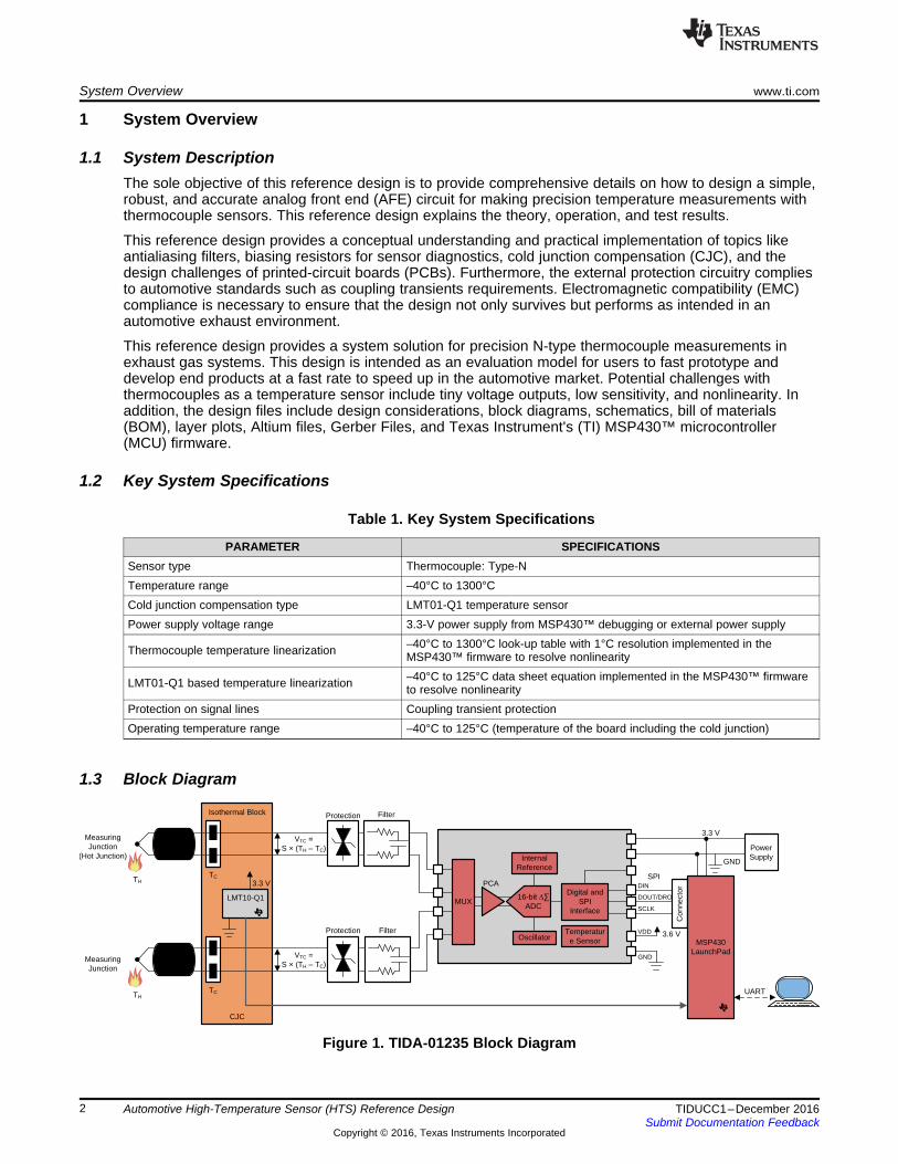
1.3 Block Diagram
Figure 1. TIDA-01235 Block Diagram

www.ti.com System Overview
3TIDUCC1–December 2016Submit Documentation Feedback
Copyright © 2016, Texas Instruments Incorporated
Automotive High-Temperature Sensor (HTS) Reference Design
The front-end circuit biases a N-type thermocouple, filters out of bandwidth noise, reads the generatedsignal, amplifies the signal, and then converts analog input voltages into CJC and linearized, 16-bit digitaltemperature readings. The module uses the National Institute of Standards and Technology (NIST)linearization tables based on the International Temperature Scale of 1990 (ITS-90) for thermocouplelinearization.
The AFE circuit offers a solution for CJC, using an LMT01-Q1 sensor. The use of LMT01-Q1 reduces theinfluence of temperature from other electronics in the systems to effectively provide good accuracy, whichis also useful when placing an isothermal block in the vicinity of thermocouples. The MPS430 MCUprovides the key computation of this AFE design. The MSP430 contains all of the software that enablesthe MCU to perform all of the intended functions. The MCU interfaces with the ADS1118-Q1 devicethrough the serial peripheral interface (SPI). Immediately after power up, the MCU performs the necessaryinitializations required to run, such as setting up the system clock, I/O port settings, enable and disableinterrupts, and the initialization of SPI engines to begin communication with the ADC. After self-initialization, the MCU initializes the internal registers of the ADC as per the design requirements alreadycaptured and implemented in software. The preceding Figure 1 shows the components of the design.
1.3.1 Highlighted Products
1.3.1.1 ADS1118-Q1The ADS1118-Q1-Q1 is a precision, low-power, 16-bit analog-to-digital converter (ADC) that provides allthe features necessary to measure the most common sensor signals. The ADS1118-Q1-Q1 integrates aprogrammable gain amplifier (PGA), voltage reference, oscillator, and high-accuracy temperature sensor.These features, along with a wide power-supply range from 2 V to 5.5 V, make the ADS1118-Q1-Q1ideally suited for thermocouple sensor-measurement applications. The ADS1118-Q1-Q1 performsconversions at data rates up to 860 samples per second (SPS).
The PGA offers input ranges from ±256 mV to ±6.144 V allowing both large and small signals to bemeasured with high resolution. An input multiplexer (MUX) allows measurement of two differential or foursingle-ended inputs. The high-accuracy temperature sensor also can be used for system-leveltemperature monitoring, or cold junction compensation for thermocouples. The ADS1118-Q1-Q1 operateseither in continuous-conversion mode, or in a single-shot mode that automatically powers down after aconversion. Single-shot mode significantly reduces current consumption during idle periods. Data istransferred through an SPI. The ADS1118-Q1-Q1 is specified from –40°C to +125°C.
1.3.1.2 LMT01-Q1The LMT01-Q1 is a high-accuracy, two-pin temperature sensor with an easy-to-use pulse count interfacewhich makes it an ideal digital replacement for PTC or NTC thermistors both on and off board in theautomotive market. The LMT01-Q1 digital-pulse count output and high accuracy over a wide temperaturerange allow pairing with any microcontroller (MCU) without concern for integrated ADC quality oravailability while minimizing software overhead. The LMT01-Q1 from TI achieves a flat ±0.5°C accuracywith very fine resolution (0.0625°C) over a wide temperature range of –20°C to 125°C without systemcalibration or hardware and software compensation.
Unlike other digital integrated circuit (IC) temperature sensors, the single-wire interface of the LMT01-Q1is designed to directly interface with a general purpose input/output (GPIO) or comparator input, therebysimplifying hardware implementation. Similarly, the LMT01-Q1s integrated electromagnetic interference(EMI) suppression and simple two-pin architecture makes it ideal for onboard and offboard temperaturesensing. The LMT01-Q1 offers all the simplicity of analog NTC or PTC thermistors with the added benefitsof a digital interface, wide specified performance, EMI immunity, and minimum processor resources.

Metal B
Metal A
TH TC
VTC =S × (TH ± TC)
+
-
Reference Junction(Cold Junction)
JC
Measuring Junction(Hot Junction)
JH
Metal B
Metal A
TH TC
Reference Junction(Cold Junction)
JC
Measuring Junction(Hot Junction)
JH
Equivalent Circuit
Metal B+ -
VTC =S × (TH ± TC)
Thermocouple Theory www.ti.com
4 TIDUCC1–December 2016Submit Documentation Feedback
Copyright © 2016, Texas Instruments Incorporated
Automotive High-Temperature Sensor (HTS) Reference Design
2 Thermocouple Theory
2.1 Thermocouple TheoryIn the automotive market, temperature is the most required parameter to measure in many places inautomotive, requires continuous measurement, monitoring, and control. The current automotive marketdemands a temperature sensor, which has a higher integration of many thermocouples in one unit at areasonably low cost to reduce the overall production costs. All temperature sensors measure temperatureby sensing a change in the material physical characteristics as a function of temperature. Temperaturesensors are available in wide varieties:• Thermocouple• Resistance temperature detector (RTD)• Thermistor• Semiconductor temperature sensor integrated circuit
The use of thermocouples in the exhaust gas temperature is increasing because of its lower cost andability to withstand higher temperatures. Thermocouples are of a simple construction, rugged, inexpensive,and one of the most commonly-used temperature transducers covering a wide range of temperatures. Athermocouple is formed when two dissimilar metal wires bind together electrically to form two junctions, asFigure 2 shows.
Figure 2. Simple Thermocouple
Whenever the two junctions formed by joining two dissimilar metals experience a temperature gradient, anopen-circuit voltage develops. The produced voltage, first discovered by the German scientist ThomasJohann Seebeck in 1821, is called “Seebeck Voltage" and this phenomenon is called the “SeebeckEffect”. Modern physics provides an explanation of the Seebeck phenomenon: The voltage potentialdevelops because free-electrons at the hot end are more thermally agitated than the free-electrons at thecooler end. The more thermally agitated electrons on the hot end begin to diffuse toward the cooler end.This redistribution of electrons creates a negative charge at the cooler end and an equal positive charge atthe hot end. The result is the production of an electrostatic-voltage between the two ends. The magnitudeand direction of the open-circuit voltage developed between the two ends is proportional to thetemperature difference; refer to the following Equation 1.

Temperature (qC)
The
rmoc
oupl
e V
olta
ge (
mV
)
-300 -200 -100 0 100 200 300 400 500 600 700 800 900 1000 1100 1200 1300 1400 1500 1600 1700 1800-10
0
10
20
30
40
50
60
70
80
D001
Type N
( )TC H CV S T T= ´ -
www.ti.com Thermocouple Theory
5TIDUCC1–December 2016Submit Documentation Feedback
Copyright © 2016, Texas Instruments Incorporated
Automotive High-Temperature Sensor (HTS) Reference Design
(1)
where• VTC is the Seebeck voltage in mV• S is the Seebeck coefficient or thermoelectric sensitivity in μV/ºC• TH is the temperature of hot junction or measuring junction in ºC• TC is the temperature of reference junction or cold junction in ºC.
When designing with thermocouples, understanding that thermocouples are bipolar is important. A bipolarthermocouple indicates a capability to produce a positive or negative voltage depending on whether or notthe measured temperature is higher or lower than the system temperature, respectively. Unlike othertemperature sensors, thermocouples do not require excitation due to their inherent voltage output.
Theoretically, all dissimilar metals exhibit the Seebeck effect, but only a few specific metal combinationsare used to make most practical thermocouple sensors. These combinations have been categorized andcharacterized into different calibration types by the National Institute of Standards and Technology (NIST).Each calibration type is designated by the capital letters indicating the composition and other differentcharacteristics, as Figure 3 shows. Based on calibration type, the thermocouple has an individualsensitivity of 40 μV/°C (for a type-N thermocouple), a temperature range, accuracy, life-span, andnonlinearity over a temperature range.
The Seebeck coefficient is a nonlinear function of temperature that causes nonlinearity in thethermocouple output voltage over the operating temperature range. Thermocouples are not uniformlylinear across a temperature range, as Figure 3 shows. Always choose a thermocouple with less variationin the Seebeck coefficient. Also note that the use of type-N thermocouples is preferable in the majority ofthe automotive market because of stability issues.
Figure 3. Thermocouple Voltage as Function of Temperature

THOT = Unknown??
J1
V1
Constantan
Copper Cu
J2Cu
V2
¨V = V1 ± V2 = 3.4 mV
Voltmeter
+
+- -
0°C Ice Bath
( )( )HOTT 3.4 mV / 40 V / C 0 C 85 C= m ° + ° = °
( )HOT COLDT V / S T= D +
THOT = Unknown??
J1
V1
Constantan
Copper Cu
J2Cu
V2
¨V = V1 ± V2
Voltmeter
+
+- -
Thermocouple Theory www.ti.com
6 TIDUCC1–December 2016Submit Documentation Feedback
Copyright © 2016, Texas Instruments Incorporated
Automotive High-Temperature Sensor (HTS) Reference Design
2.2 Cold Junction Compensation (CJC)Thermocouples measure the temperature difference between hot and cold junctions. Thermocouples donot measure the absolute temperature at one junction, as Figure 4 shows. The cold junction is alsoreferred to as a reference junction.
Thermocouples are created with leads at the meter connection. In the printed-circuit board (PCB), theseunwanted thermocouples are one of the biggest concerns. Each dissimilar metal connection creates a newthermocouple as one proceeds from measuring end to wire connector, to solder, to copper PCB trace, toIC pin, to bonding wire, and to chip or die contact. However, if the signal is differential, and each of thethermocouple pairs are at the same temperature, then the thermocouple voltages cancel out and have nonet effect on the measurement. Therefore, the net voltage error added by these connections is zero.
Figure 4. Unwanted Thermocouple Junction
The next step is to determine what is required to calculate the temperature (T HOT) of measuring junctionJ1.The following Equation 2 indicates that to find out the temperature of hot junction of a thermocouplerequires knowing the temperature of the cold junction. The cold junction of a thermocouple usually is keptin an ice bath (see Figure 5) to keep it at a known reference temperature of 0°C, which is another reasonit is called as cold junction. In reality, it is impractical and inconvenient in most applications to provide atrue ice-point reference. The NIST thermocouple reference table also assumes that the cold junction is at0°C.
(2)
For example, if a T-type thermocouple produces an open circuit voltage of 3.4 mV with its cold junctionreference temperature maintained at 0°C. The next step is to determine the temperature of its hot junction.Assume that a Seebeck coefficient of a T-type thermocouple is 40 μV/°C (see Equation 3).
(3)
Figure 5. Measuring Absolute Temperature Using 0°C Ice Bath
Knowing the cold junction reference temperature is necessary to determine the correct absolutetemperature at the measuring junction. An additional measurement is then mandatory to determine thecold junction reference temperature because practically it is not possible to provide ice bath. The morepractical and logical approach is to use some other type of direct-reading, temperature sensor meanscapable of absolute measurements (not relative measurements as with an RTD). Use a thermistor orsensor IC to measure the temperature at the reference junction and then use it to compute thetemperature at the measuring junction of a thermocouple. This technique is called cold junctioncompensation (CJC). This design uses a sensor IC (LMT01-Q1) for the compensation.
www.ti.com Thermocouple Theory
7TIDUCC1–December 2016Submit Documentation Feedback
Copyright © 2016, Texas Instruments Incorporated
Automotive High-Temperature Sensor (HTS) Reference Design
2.3 Thermocouple Input Signal ConditioningThe use of thermocouples, despite their prevalence in the field of engineering, is often misunderstood andcan result in many design challenges due to issues such as small output voltage, low sensitivity, andnonlinearity across the temperature range. Achieving an overall system accuracy of ±1ºC or better isdifficult because of these signal-conditioning issues. Users must design the interface of a thermocouplesensor analog front-end (AFE) with extreme care to achieve a sufficient level of accuracy. A thermocouplesignal chain consists of a thermocouple sensor in the front, a thermocouple connector, an isothermalblock, overvoltage protection, biasing resistors, an antialiasing filter, an amplifier, an ADC, and sensordata linearization in the software. This AFE circuit addresses all of the challenges associated with themeasuring of thermocouple temperature.
2.3.1 Input Filter DesignThe main goal of the filter design is to keep the filter initial error contribution to the total error comparableto or smaller than the initial error of the thermocouple sensor. Because of the manufacturing limitations ofthe type-N thermocouple, which is mainly related to the purity of materials, the initial error of thethermocouple sensor (tolerance class 1) is typically less than 1.5°C and from –40°C to 1300°C. The initialerror is also better than 0.4% up to 1300°C, which is the maximum range of thermocouple temperatures.
Signal conditioning is critical in any design. Any ADC, regardless of architecture, requires some amount offiltering on the inputs to reduce noise in the system, which is because of the effects of aliasing. The digitalfilter in delta-sigma (ΔΣ) ADCs significantly reduces the requirements of an external analog filter, but stillrequires some filtering. A simple filter, such as the one that shows, creates a balanced differential filter.
The filter design using the ADS1118-Q1-Q1 device employs a simple first-order filter. The use of this first-order filter is due to the expected small-form factor and cost requirements of this reference design. Usersimplementing this filter can easily sequence the filter into higher-order filters to provide a greater immunityto high-frequency noise.
Refer to the TIDA-00168 reference design [3] for a detailed description of the input filter design.
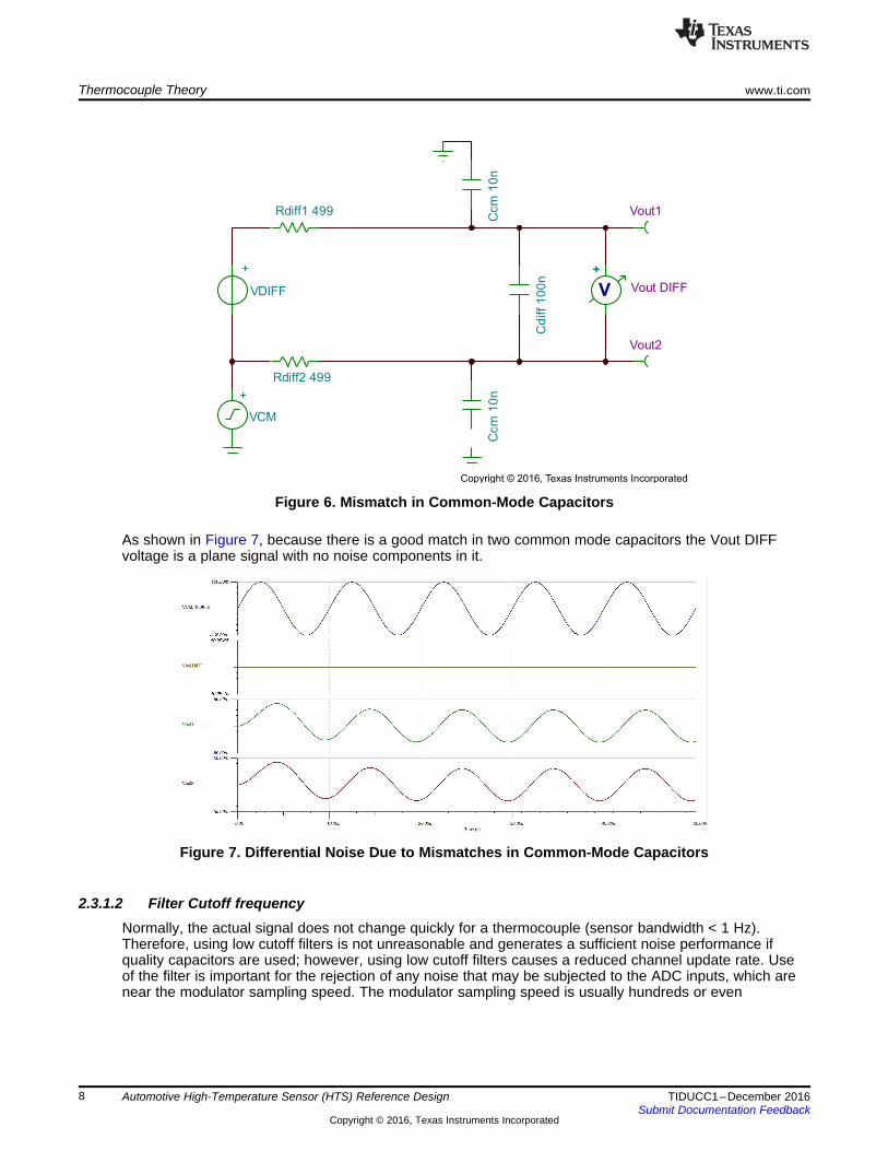
2.3.1.1 Selecting Differential-Mode and Common-Mode Capacitor RatioThe differential filter is also great for reducing both common-mode and differential noise components. Theresistors used to develop the filter also serve to limit current to the inputs of any device that follows thefilter. When sized accordingly, the resistors enable better functionality to the inputs, protection againstelectrostatic discharge (ESD), and long-term overvoltage conditions. The filter shown in is an example of astructure commonly used for differential signals. A few important points require consideration whenselecting components. To avoid differential noise caused by mismatches in the common-mode capacitors,industry standards recommend using a differential capacitor that is at least ten times greater than thecommon-mode capacitors.
Rdiff2 499
+
VCM
V
+
Vout DIFF
Vout1
Vout2
Rdiff1 499
+
VDIFF
Cd
iff
10
0n
Ccm
10
nC
cm
10
n
Copyright © 2016, Texas Instruments Incorporated
Thermocouple Theory www.ti.com
8 TIDUCC1–December 2016Submit Documentation Feedback
Copyright © 2016, Texas Instruments Incorporated
Automotive High-Temperature Sensor (HTS) Reference Design
Figure 6. Mismatch in Common-Mode Capacitors
As shown in Figure 7, because there is a good match in two common mode capacitors the Vout DIFFvoltage is a plane signal with no noise components in it.
Figure 7. Differential Noise Due to Mismatches in Common-Mode Capacitors
2.3.1.2 Filter Cutoff frequencyNormally, the actual signal does not change quickly for a thermocouple (sensor bandwidth < 1 Hz).Therefore, using low cutoff filters is not unreasonable and generates a sufficient noise performance ifquality capacitors are used; however, using low cutoff filters causes a reduced channel update rate. Useof the filter is important for the rejection of any noise that may be subjected to the ADC inputs, which arenear the modulator sampling speed. The modulator sampling speed is usually hundreds or even

( )
( )
CMF1 F2 DIFF
CMF1 F2 DIFF
1 1
C 100002 256 kHz R R C
2
11
C2 25.6 kHz R R C
2
=æ ö
p ´ ´ + ´ +ç ÷è ø
=æ ö
p ´ ´ + ´ +ç ÷è ø
( )DIFF F1 F2
2 256 kHz
R R R
· v = p ´
· = +
2
DIFF DIFF
CM
1 1
100001
1 R C2C
=
æ öæ ö+ v +ç ÷ç ÷ç ÷
è øè ø
O
DIFF DIFF CM1
U 1A
11 j R C CU
2
××××
××= =
æ ö+ v +ç ÷
è ø
www.ti.com Thermocouple Theory
9TIDUCC1–December 2016Submit Documentation Feedback
Copyright © 2016, Texas Instruments Incorporated
Automotive High-Temperature Sensor (HTS) Reference Design
thousands of times higher than the actual ADC output data rate. The data converter cannot digitally rejectnoises of higher frequencies. The use of analog input filtering is required to reject noises of higherfrequencies. ΔΣ ADCs specify the sampling frequency of the modulator to allow external filters to bedesigned accordingly. The ADS1118-Q1-Q1 device, for example, has a modulator sampling frequency of256 kHz.
The input filter also performs as an antialiasing filter. In most systems, users can calibrate out errorsintroduced through input filters. However, for this uncalibrated example, the ADS1118-Q1-Q1 device hasroughly 10 MΩ of differential input impedance, which increases the gain error as the sensor output andfilter impedances increase. When selecting the filter for this design there is a trade-off between loweringthe cutoff and using small-value components. Ideally, due to the low bandwidth of the sensor ( <1 Hz),users prefer a thermocouple design with a lower cutoff frequency and a higher-order filter. However,designing a high-order passive filter that is aggressive introduces large resistances in front of the ADC,which interacts with the differential input impedance of the ADS1118-Q1-Q1 device.
The inside digital filter cannot dispose of the aliasing signal brought on by the modulator; however, theinput filter can act as an antialiasing filter. The goal of this design is to keep the signal rejection at 256 kHzand at least –80 dB. The –80 dB attenuation is arbitrary and depends on the expected noise in theenvironment where the system is deployed. The –80 dB shows that the injected undesirable signal of5 mV attenuates to 0.5 μV.
The filter must be able to reduce noise to 256 kHz by a factor of 10000. The desired rejection is at256 kHz of 80 dB. Calculate a cutoff frequency to achieve this rejection. Because the first-order filter inthis design rejects at 20 dB per decade, the corresponding –3-dB frequency would be four decades downfrom 256 kHz or 25.6 Hz. The transfer function of the filter is calculated in Equation 4:
(4)
So, the cutoff frequency of the filter is 25.6 Hz.
where• RDIFF = differential resistance• CDIFF = differential capacitance• CCM = common-mode capacitance• RF1 = resistance on single end• RF2 = resistance on other single end.

Thermocouple Theory www.ti.com
10 TIDUCC1–December 2016Submit Documentation Feedback
Copyright © 2016, Texas Instruments Incorporated
Automotive High-Temperature Sensor (HTS) Reference Design
2.3.2 PGA Operation and Common-Mode Voltage LimitationThe PGA offers input ranges from ±256 mV to ±6.144 V, allowing both large and small signals to bemeasured with high resolution. The ADS1118-Q1-Q1 performs conversions at data rates up to860 samples per second (SPS). An input multiplexer (MUX) allows measurement of two differential or foursingle-ended inputs. A type N thermocouple couple gives out the voltages from –1.269 mV to47.477 mV, so select the range in such a way to match this range. Choosing ±256 mV is clearly a betterchoice that allows the designer to make the most of this specification.
2.3.3 Biasing ResistorsIn the case of a floating signal source and differential measurement, take care to ensure that the common-mode voltage level of the signal remains in the common-mode input range of the measurement devicewith respect to the measurement system ground. In the input stage of a data acquisition device, the inputbias currents can move the voltage level of the floating source out of the valid range. Use resistors to biasthis voltage to a reference, as Figure 8 shows.
Figure 8. Thermocouple Biasing Options Using Pullup and Pulldown Resistors
The +AVDD = 3.3 V of system voltage.
These resistors are called bias resistors and provide a DC path from the device inputs to themeasurement system ground. Bias resistors must have a large enough value to allow the source to floatwith respect to the measurement system ground and not load the signal source. Likewise, the biasingresistors RB1 and RB2 are used to set the common-mode voltage of the thermocouple within the specifiedcommon-mode voltage range of the PGA (in this example, to mid-supply AVDD / 2). Mid-supply AVDD / 2is often an ideal common-mode voltage for most devices like ADCs, operational amplifiers, and PGAs. Ifthe application requires the thermocouple to be biased to GND, a bipolar supply (for example,AVSS = –2.5 V and AVDD = +2.5 V) must be used for the ADS1118-Q1-Q1 device to meet the common-mode voltage requirement.
Understanding the consequence of not using biasing resistors is important. Without the biasing resistors,the thermocouple output-voltage is differential. If not biased to any reference level, the common-modevoltage can be anywhere from AVSS to AVDD (in this example, 0 V to 3.3 V), thus indicating that thecondition for common-mode voltage can be violated. Consequently, the non-ideal common-mode rejectionratio (CMRR) of the device results in an input offset voltage error.

Copyright © 2016, Texas Instruments Incorporated
www.ti.com Thermocouple Theory
11TIDUCC1–December 2016Submit Documentation Feedback
Copyright © 2016, Texas Instruments Incorporated
Automotive High-Temperature Sensor (HTS) Reference Design
To determine the common-mode input voltage set by the design, replace the thermocouple by itsThevenin’s equivalent circuit where VTC is a function of the Seebeck coefficient and the temperaturedifference (ΔT) between the two junctions, as the preceding Figure 8 shows. RTC is the thermocouple wireresistance, which is a function of wire resistivity, length, and gauge. This design has two options forconnecting the biasing resistors to the thermocouple lead wires, as Figure 8 shows. Both options offerdifferent advantages and disadvantages. The current design uses option A. Refer to the TIDU574reference design[3] for a detailed description of why to choose option A.
2.4 Cold Junction Compensation (CJC)The current design uses LMT01-Q1 for CJC. To measure the temperature of the cold junction, place theLMT01-Q1 device in close vicinity to the thermocouple connector ends, as Figure 9 shows. A groundisolation barrier is provided to share the effect of the isothermal block from the other components thermalbehavior. The voltage measured across the temperature sensor (LMT01-Q1) is proportional to thetemperature of the isothermal block, which is determined by the characteristic equation of LMT01-Q1. AsFigure 10 shows, one end of LMT01-Q1 is connected to ground to have at least one potential to maintainthe isothermal condition chosen for this configuration. Output resistor 100K along with the transistor level-shifter configuration; the LMT01-Q1 output pulses in the range of 3.3 V. Pulsing can be achieved with thehelp of the MCUs GPIO and timers or Interrupts.
Figure 9. Placement of LMT01-Q1 in Isothermal Block for CJC
Figure 10. LMT01-Q1 Connection Schematic

2 channels of thermocouples(Maintain symmetry)
Separation of other components from isothermal block
Maximum of the components are bottom side
Symmetry on ADC input filters
LMT01 on Top layer/bottom layer should not have any components
in isothermal block area
Separation of isothermal block from other sections of the board
Thermocouple Theory www.ti.com
12 TIDUCC1–December 2016Submit Documentation Feedback
Copyright © 2016, Texas Instruments Incorporated
Automotive High-Temperature Sensor (HTS) Reference Design
2.5 PCB GuidelinesOne of the challenges for the thermocouple design is to design an optimal layout. Section 2.4 describesthe CJC block layout considerations. As Figure 11 and Figure 12 show, ADC input sections must besymmetrical to nullify the effects of unwanted, small thermocouples junctions and EMI noise. Theisothermal block is completely separated from the other section of the board to nullify the effect oftemperature on the isothermal block. The bottom layer has most of the components and the designer mustensure that none of the components are in the vicinity of the isothermal block.
Figure 11. Top Layer
Figure 12. Bottom Layer
TC1
TC2
Filter signal conditioning
Filter signal conditioning
ADS1118-Q1
Temperature sensor signal conditioning
CJC temperature
LMT01
www.ti.com Getting Started Hardware and Software
13TIDUCC1–December 2016Submit Documentation Feedback
Copyright © 2016, Texas Instruments Incorporated
Automotive High-Temperature Sensor (HTS) Reference Design
3 Getting Started Hardware and Software
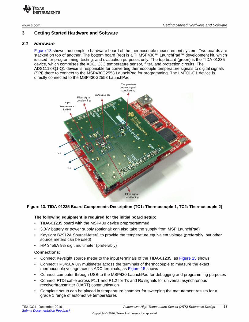
3.1 HardwareFigure 13 shows the complete hardware board of the thermocouple measurement system. Two boards arestacked on top of another. The bottom board (red) is a TI MSP430™ LaunchPad™ development kit, whichis used for programming, testing, and evaluation purposes only. The top board (green) is the TIDA-01235device, which comprises the ADC, CJC temperature sensor, filter, and protection circuits. TheADS1118-Q1-Q1 device is responsible for converting thermocouple temperature signals to digital signals(SPI) there to connect to the MSP430G2553 LaunchPad for programming. The LMT01-Q1 device isdirectly connected to the MSP430G2553 LaunchPad.
Figure 13. TIDA-01235 Board Components Description (TC1: Thermocouple 1, TC2: Thermocouple 2)
The following equipment is required for the initial board setup:• TIDA-01235 board with the MSP430 device preprogrammed• 3.3-V battery or power supply (optional: can also take the supply from MSP LaunchPad)• Keysight B2912A SourceMeter® to provide the temperature equivalent voltage (preferably, but other
source meters can be used)• HP 3458A 8½ digit multimeter (preferably)
Connections:• Connect Keysight source meter to the input terminals of the TIDA-01235, as Figure 15 shows• Connect HP3458A 8½ multimeter across the terminals of thermocouple to measure the exact
thermocouple voltage across ADC terminals, as Figure 15 shows• Connect computer through USB to the MSP430 LaunchPad for debugging and programming purposes• Connect FTDI cable across P1.1 and P1.2 for Tx and Rx signals for universal asynchronous
receiver/transmitter (UART) communication• Complete setup can be placed in temperature chamber for sweeping the maturement results for a
grade 1 range of automotive temperatures

MCU
CJC Temperature
Sensor
ADC
Thermocouple
Voltage
Temperature
Sensor
Wµo���W�
Temperature Result
VTC
ë�Pulses
TActualTActualTCJC
s�W��d
TTC
Getting Started Hardware and Software www.ti.com
14 TIDUCC1–December 2016Submit Documentation Feedback
Copyright © 2016, Texas Instruments Incorporated
Automotive High-Temperature Sensor (HTS) Reference Design
3.2 SoftwareAn MSP430G2553 LaunchPad is used to program in the Embedded C language. TI recommends to useCode Composer Studio™ (CCS) software when dealing with MSP430 LaunchPads. CCS is an integrateddevelopment environment (IDE) for TI embedded processor families. CCS comprises a suite of tools usedto develop and debug embedded applications. CCS includes compilers for each of TI's device families,source code editor, project build environment, debugger, profiler, simulators, real-time operating system,and many other features. The intuitive IDE provides a single-user interface that guides through each stepof the application development flow.
Figure 14 shows the flow diagram of the working program. The ADC on the TIDA-01235 converts thethermocouple voltage to equivalent SPI codes and, using look-up tables, these codes are converted intoreal temperature values (TTC). By using a characteristic equation, the LMT01-Q1 pulse information isconverted into temperature (TCJC). Add both thermocouple temperature (TTC) and cold junction temperature(TCJC) to obtain the final, actual temperature (TActual) value.
Figure 14. Software Flow Diagram

Keysight Source Meter
B2912A
HP34588½ digit
multimeter
Temperature Chamber
Code Composer Studio¡
PC/Laptop
USB
www.ti.com Testing and Results
15TIDUCC1–December 2016Submit Documentation Feedback
Copyright © 2016, Texas Instruments Incorporated
Automotive High-Temperature Sensor (HTS) Reference Design
4 Testing and Results
4.1 Test SetupFigure 15 shows the test setup. connect the diagram as shown to start the setup. All the test results areperformed using channel 1 of the ADC.
Thermocouple equivalent voltages are provided using a Keysight Source meter; connect this meter tochannel 1 of the ADC, as Figure 15 shows. An 8½ digit multimeter is used to measure the exact amountof voltage applied, so connect the multimeter to the same terminals of ADC channel 1.The complete setupis then placed inside a temperature chamber and UART signals are transmitted to the PC through an FTDIcable.
Figure 15. Testing Equipment Connection
4.2 Test PlanThe main purpose of thermocouple testing is to estimate the accuracy of ADC and CJC channels. Everythermocouple system generally has two channels, namely a thermocouple channel and an externaltemperature sensor channel. The total error of a thermocouple is the sum of these errors. As previouslyaddressed, this reference design has two boards: the MSP430 LaunchPad and TIDA-01235 referencedesign board. When taking temperature measurements, the MSP430 is kept outside and the temperaturechamber and the TIDA-01235 board is kept inside. Both boards are connected through SPI. The MSPcommunicates with the computer through UART.
The MSP430 provides the pure temperature cycle (TC) temperature without the calculation of the coldjunction. Section 4.3 shows all of the tests. Use the test setup as shown in Figure 15. The equivalentthermocouple voltages are applied from –1.269 mV to 47.477 mV in several steps.
The test plan is divided into three cases to calculate the thermocouple accuracy:• Thermocouple channel accuracy (ADS11118-Q1 accuracy)• Thermocouple channel accuracy (ADC1118-Q1 accuracy) plus CJC channel accuracy (LMT01-Q1
accuracy)• CJC channel accuracy (LMT01-Q1 accuracy)

Testing and Results www.ti.com
16 TIDUCC1–December 2016Submit Documentation Feedback
Copyright © 2016, Texas Instruments Incorporated
Automotive High-Temperature Sensor (HTS) Reference Design
4.2.1 Thermocouple Channel Accuracy (ADS11118-Q1 Accuracy)To test the accuracy along the thermocouple channel, thermocouple temperature equivalent voltages(–1.269 mV to 47.477 mV) are provided in several steps with an SMU on channel 1 of the ADC. TheADS1118-Q1-Q1 device interprets these voltages and converts SMU voltages into respectivetemperatures using look-up tables. The MSP430 delivers the temperature values through UART. Thedifference between the SMU input voltage and MSP430 output voltage estimates for the error.
4.2.2 Thermocouple Channel Accuracy (ADC1118-Q1 Accuracy) Plus CJC Channel Accuracy(LMT01-Q1 Accuracy)
To test the accuracy along the thermocouple channel plus CJC channel, thermocouple temperatureequivalent voltages (–1.269 mV to 47.477 mV) are provided with an SMU on channel 1 of the ADC. TheADS1118-Q1-Q1 device interprets these voltages and uses the MSP430 converts these voltages intotemperature using look-up tables. The MSP430 through UART delivers the temperature values. Thedifference between the SMU input voltage and MSP430 output voltage estimates for the error. LMT01-Q1pulses are converted into temperature using the characteristic equation provided in the LMT01-Q1datasheet.
TC temperature is added with the CJC temperature and can estimate the error using input and outputtemperature values.
4.2.3 CJC Channel Accuracy (LMT01-Q1 Accuracy)LMT01-Q1 pulses are converted into temperature using the characteristic equation provided in theLMT01-Q1 datasheet. The temperature chamber is maintained at various temperatures (from –40°C to125°C), and per measurement, 30 samples have been taken to estimate the LMT01-Q1 error. A graph isplotted between the LMT01-Q1 temperature and the deviation from the original value.
4.3 Temperature Error of Thermocouple Channel With and Without CJCA thermocouple type N over a temperature range of –40ºC to +1300ºC produces a corresponding outputvoltage from –1.269 mV to 47.477 mV. Voltage is applied across thermocouple input channels and theoutput is recorded in the computer. The TIDA-01235 board remains in the temperature chamber andestimates errors from –40ºC to +125ºC. Figure 16 shows the test setup. The source meter and multimeterare automated in such a way to feed the thermocouple voltage from –1.269 mV to 47.477 mV in differentsteps.
Figure 16. Test Setup

Thermocouple Temperature (qC)
Tem
pera
tre
Err
or (q
C)
-200 0 200 400 600 800 1000 1200 1400-2.5
-2.0
-1.5
-1.0
-0.5
0.0
0.5
1.0
1.5
2.0
2.5
D002
Without Calibration at 25 qCWith Calibration at 25 qC
Thermocouple Temperature (qC)
Tem
pera
tre
Err
or (q
C)
-200 0 200 400 600 800 1000 1200 1400-2.5
-2.0
-1.5
-1.0
-0.5
0.0
0.5
1.0
1.5
2.0
2.5
D003
Without Calibration at 25 qCWith Calibration at 25 qC
www.ti.com Testing and Results
17TIDUCC1–December 2016Submit Documentation Feedback
Copyright © 2016, Texas Instruments Incorporated
Automotive High-Temperature Sensor (HTS) Reference Design
The temperature chamber is set to –36ºC, 0ºC, 25ºC, 75ºC, and 125ºC and the thermocouple temperatureaccuracy is analyzed at intermittent temperatures between the temperature range from –40ºC to +1300ºCat equivalent voltages of –1.269 mV to 47.477 mV.
Graphs terminologyError (TC): Error_TC is defined as the total ADC channel error. Error_TC includes the ADC gain, offset,and linearity error but excludes the error due to CJC from the LMT01-Q1 device. The exact temperaturesare calculated from the thermocouple output voltage using look-up tables.
Error (TC + CJC): Error_TC + CJC is defined as the total error including ADC channel error and LMT01-Q1 error. Error_TC includes the ADC gain, offset, and linearity error, which also includes the error due toCJC from the LMT01-Q1 device. The corresponding temperatures are calculated from the thermocoupleoutput voltage using look-up tables and the LMT01-Q1 characteristic equation.
The system accuracy can be further improved by performing a gain calibration. The easiest method ofcalibration is a one-point gain calibration, which is performed by finding the fraction between the maximumoutput and maximum input and then multiplying the total set of results with this number. This one-pointcalibration is performed at room temperature. Additional calibration points at different ambienttemperatures increase the accuracy of the results; however, this step has not been performed in thisguide. For the gain calibration, several measurements were taken for a thermocouple temperature of1300°C. The resulting ADC codes were averaged and compared with the ideal, expected ADC code.
Figure 17 through Figure 27 show the measurement results. A voltage from –1.269 mV to 47.477 mV isapplied across the thermocouple output terminals when the LMT01-Q1 device is maintained at a constanttemperature.
In Figure 17 and Figure 18, the temperature error at 25°C with a gain and offset correction factor(Error_TC) has improved compared to the error without the gain and offset calibration factor(Error_TC + CJC). The error of the thermocouple channel at 25°C is now minimized across the entireinput range (–40°C to +1300°C), comparing the results without gain and offset calibration with the resultswith gain and offset calibration. As is visible in the plots, the graphs have been rotated by the calibrationfactor around the crossing point of the curves, which is just calibrated for 25°C. The same process cannow also be done for other temperature points.
Figure 17. Temperature Error at 25°C for TC Channel Figure 18. Temperature Error at 25°C for TC + CJCChannel
In Figure 19 and Figure 20, the temperature error at 0°C with gain and offset correction factor (Error_TC)has improved in comparison to the error without the gain and offset correction factor (Error_TC + CJC).The error of the thermocouple channel at 0°C is now minimized across the entire input range (–40°C to+1300°C), comparing the results without gain and offset calibration with the results with gain and offsetcalibration. As is visible in the plots, the graphs have been rotated by the calibration factor around thecrossing point of the curves.

Thermocouple Temperature (qC)
Tem
pera
tre
Err
or (q
C)
-200 0 200 400 600 800 1000 1200 1400-2.5
-2.0
-1.5
-1.0
-0.5
0.0
0.5
1.0
1.5
2.0
2.5
D006
Without Calibration at 25 qCWith Calibration at 25 qC
Thermocouple Temperature (qC)
Tem
pera
tre
Err
or (q
C)
-200 0 200 400 600 800 1000 1200 1400-2.5
-2.0
-1.5
-1.0
-0.5
0.0
0.5
1.0
1.5
2.0
2.5
D007
Without Calibration at 25 qCWith Calibration at 25 qC
Thermocouple Temperature (qC)
Tem
pera
tre
Err
or (q
C)
-200 0 200 400 600 800 1000 1200 1400-2.5
-2.0
-1.5
-1.0
-0.5
0.0
0.5
1.0
1.5
2.0
2.5
D004
Without Calibration at 25 qCWith Calibration at 25 qC
Thermocouple Temperature (qC)
Tem
pera
tre
Err
or (q
C)
-200 0 200 400 600 800 1000 1200 1400-2.5
-2.0
-1.5
-1.0
-0.5
0.0
0.5
1.0
1.5
2.0
2.5
D005
Without Calibration at 25 qCWith Calibration at 25 qC
Testing and Results www.ti.com
18 TIDUCC1–December 2016Submit Documentation Feedback
Copyright © 2016, Texas Instruments Incorporated
Automotive High-Temperature Sensor (HTS) Reference Design
Figure 19. Temperature Error at 0°C for TC Channel Figure 20. Temperature Error at 0°C for TC + CJCChannel
In Figure 21 and Figure 22, the temperature error at 75°C with gain and offset correction factor (Error_TC)has improved in comparison to the error without the gain and offset correction factor (Error_TC + CJC).The error of the thermocouple channel at 75°C is now minimized across the entire input range (–40°C to+1300°C), comparing the results without gain and offset calibration with the results with gain and offsetcalibration. As is visible in the plots, the graphs have been rotated by the calibration factor around thecrossing point of the curves.
Figure 21. Temperature Error at 75°C for TC Channel Figure 22. Temperature Error at 75°C forTC + CJC Channel

Thermocouple Temperature (qC)
Tem
pera
tre
Err
or (qC
)
-200 0 200 400 600 800 1000 1200 1400-0.8
-0.6
-0.4
-0.2
0
0.2
0.4
0.6
0.8
D009
Temperature Error (qC) at -40qCTemperature Error (qC) at 0qCTemperature Error (qC) at 25qCTemperature Error (qC) at 50qCTemperature Error (qC) at 75qCTemperature Error (qC) at 125qC
Thermocouple Temperature (qC)
Tem
pera
tre
Err
or (qC
)
-200 0 200 400 600 800 1000 1200 1400-2
-1.5
-1
-0.5
0
0.5
1
1.5
2
2.5
3
D008
Temperature Error (qC) at �40qCTemperature Error (qC) at 0qCTemperature Error (qC) at 25qCTemperature Error (qC) at 50qCTemperature Error (qC) at 100qCTemperature Error (qC) at 125qC
www.ti.com Testing and Results
19TIDUCC1–December 2016Submit Documentation Feedback
Copyright © 2016, Texas Instruments Incorporated
Automotive High-Temperature Sensor (HTS) Reference Design
Figure 23 represents the thermocouple channel error for a temperature range from –40°C to +125°Cwithout gain and offset calibration.
Figure 23. Thermocouple Channel Error in ºC Without Gain and Offset Calibration
Figure 24 represents the thermocouple channel error for a temperature range from –40°C to +125°C withgain and offset calibration.
Figure 24. Thermocouple Channel Plus CJC Error in ºC With Gain and Offset Calibration
The preceding Figure 23 and Figure 24 show the error by taking the entire set of data again over theambient temperature –40°C to +125°C; however, with a gain and offset correction factor, the resultingtemperature error can be seen in Figure 24. Comparing the results without gain calibration (Figure 23)with the results with gain and offset calibration (Figure 24), it is visible that the graphs have been rotatedby the calibration factor around the crossing point of the three curves and with an observable that error isless than ±1°C.
Samples
Err
or (qC
)
0 2 4 6 8 10 12 14 16 18 20 22 24 26 28 30-1.0
-0.8
-0.6
-0.4
-0.2
0.0
0.2
0.4
0.6
0.8
1.0
D011
Samples
Err
or (qC
)
0 2 4 6 8 10 12 14 16 18 20 22 24 26 28 30-1.0
-0.8
-0.6
-0.4
-0.2
0.0
0.2
0.4
0.6
0.8
1.0
D010
Testing and Results www.ti.com
20 TIDUCC1–December 2016Submit Documentation Feedback
Copyright © 2016, Texas Instruments Incorporated
Automotive High-Temperature Sensor (HTS) Reference Design
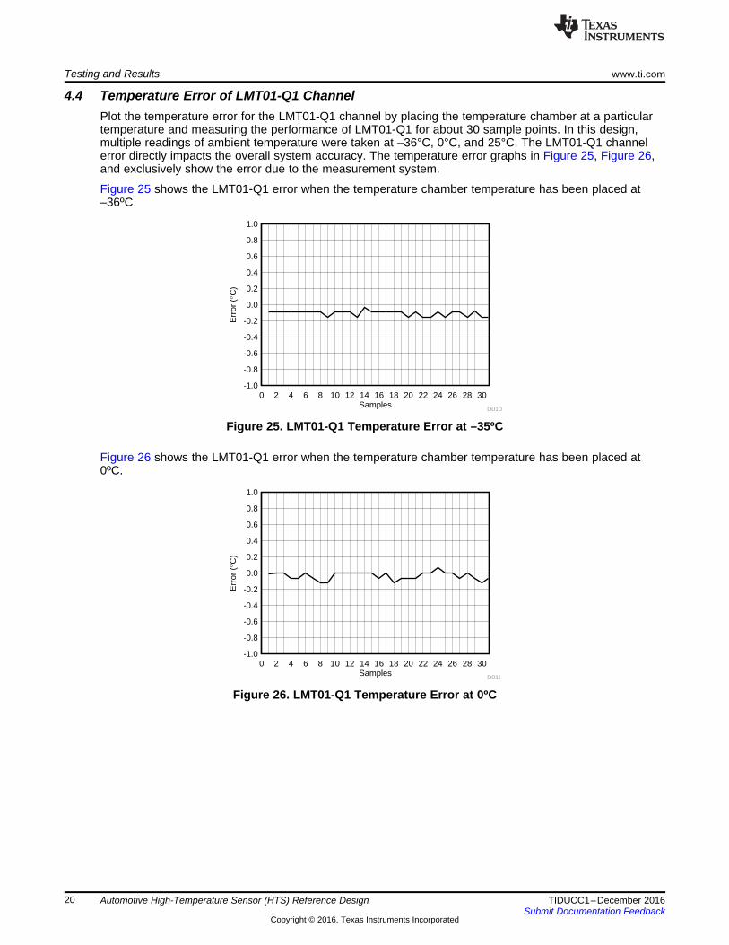
4.4 Temperature Error of LMT01-Q1 ChannelPlot the temperature error for the LMT01-Q1 channel by placing the temperature chamber at a particulartemperature and measuring the performance of LMT01-Q1 for about 30 sample points. In this design,multiple readings of ambient temperature were taken at –36°C, 0°C, and 25°C. The LMT01-Q1 channelerror directly impacts the overall system accuracy. The temperature error graphs in Figure 25, Figure 26,and exclusively show the error due to the measurement system.
Figure 25 shows the LMT01-Q1 error when the temperature chamber temperature has been placed at–36ºC
Figure 25. LMT01-Q1 Temperature Error at –35ºC
Figure 26 shows the LMT01-Q1 error when the temperature chamber temperature has been placed at0ºC.
Figure 26. LMT01-Q1 Temperature Error at 0ºC

Samples
Err
or (qC
)
0 2 4 6 8 10 12 14 16 18 20 22 24 26 28 30-1.0
-0.8
-0.6
-0.4
-0.2
0.0
0.2
0.4
0.6
0.8
1.0
D012
www.ti.com Testing and Results
21TIDUCC1–December 2016Submit Documentation Feedback
Copyright © 2016, Texas Instruments Incorporated
Automotive High-Temperature Sensor (HTS) Reference Design
Figure 27 shows the LMT01-Q1 error when the temperature chamber temperature has been placed at25ºC.
Figure 27. LMT01-Q1 Temperature Error at 25ºC

Design Files www.ti.com
22 TIDUCC1–December 2016Submit Documentation Feedback
Copyright © 2016, Texas Instruments Incorporated
Automotive High-Temperature Sensor (HTS) Reference Design
5 Design Files
5.1 SchematicsTo download the schematics, see the design files at TIDA-01235.
5.2 Bill of MaterialsTo download the bill of materials (BOM), see the design files at TIDA-01235.
5.3 PCB Layout Recommendations
5.3.1 Layout PrintsTo download the layer plots, see the design files at TIDA-01235.
5.4 Altium ProjectTo download the Altium project files, see the design files at TIDA-01235.
5.5 Gerber FilesTo download the Gerber files, see the design files at TIDA-01235.
5.6 Assembly DrawingsTo download the assembly drawings, see the design files at TIDA-01235.
6 Software FilesTo download the software files, see the design files at TIDA-01235.
7 Related Documentation
1. Texas Instruments, Precision Thermocouple Measurement with the ADS1118-Q1, Application Report(SBAA189)
2. Texas Instruments, Isolated Loop Powered Thermocouple Transmitter,TIDA-00189 Design Guide (TIDU449)
3. Texas Instruments,Thermocouple AFE Using RTD or Integrated Temperature Sensor for Cold JunctionCompensation (CJC)TIDA-00168 Design Guide (TIDU574)
7.1 TrademarksMSP430, LaunchPad, Code Composer Studio are trademarks of Texas Instruments.
8 About the AuthorSANDEEP TALLADA is a systems engineer at Texas Instruments. As a member of the AutomotiveSystems Engineering team, Sandeep focuses on powertrain end-equipment and creating subsystemreference designs. He brings to this role experience in sensor systems technology. Sandeep earned hismaster of science in sensor systems technology from the University of Applied Sciences Karlsruhe,Germany.

IMPORTANT NOTICE FOR TI REFERENCE DESIGNS
Texas Instruments Incorporated (‘TI”) reference designs are solely intended to assist designers (“Designer(s)”) who are developing systemsthat incorporate TI products. TI has not conducted any testing other than that specifically described in the published documentation for aparticular reference design.TI’s provision of reference designs and any other technical, applications or design advice, quality characterization, reliability data or otherinformation or services does not expand or otherwise alter TI’s applicable published warranties or warranty disclaimers for TI products, andno additional obligations or liabilities arise from TI providing such reference designs or other items.TI reserves the right to make corrections, enhancements, improvements and other changes to its reference designs and other items.Designer understands and agrees that Designer remains responsible for using its independent analysis, evaluation and judgment indesigning Designer’s systems and products, and has full and exclusive responsibility to assure the safety of its products and compliance ofits products (and of all TI products used in or for such Designer’s products) with all applicable regulations, laws and other applicablerequirements. Designer represents that, with respect to its applications, it has all the necessary expertise to create and implementsafeguards that (1) anticipate dangerous consequences of failures, (2) monitor failures and their consequences, and (3) lessen thelikelihood of failures that might cause harm and take appropriate actions. Designer agrees that prior to using or distributing any systemsthat include TI products, Designer will thoroughly test such systems and the functionality of such TI products as used in such systems.Designer may not use any TI products in life-critical medical equipment unless authorized officers of the parties have executed a specialcontract specifically governing such use. Life-critical medical equipment is medical equipment where failure of such equipment would causeserious bodily injury or death (e.g., life support, pacemakers, defibrillators, heart pumps, neurostimulators, and implantables). Suchequipment includes, without limitation, all medical devices identified by the U.S. Food and Drug Administration as Class III devices andequivalent classifications outside the U.S.Designers are authorized to use, copy and modify any individual TI reference design only in connection with the development of endproducts that include the TI product(s) identified in that reference design. HOWEVER, NO OTHER LICENSE, EXPRESS OR IMPLIED, BYESTOPPEL OR OTHERWISE TO ANY OTHER TI INTELLECTUAL PROPERTY RIGHT, AND NO LICENSE TO ANY TECHNOLOGY ORINTELLECTUAL PROPERTY RIGHT OF TI OR ANY THIRD PARTY IS GRANTED HEREIN, including but not limited to any patent right,copyright, mask work right, or other intellectual property right relating to any combination, machine, or process in which TI products orservices are used. Information published by TI regarding third-party products or services does not constitute a license to use such productsor services, or a warranty or endorsement thereof. Use of the reference design or other items described above may require a license from athird party under the patents or other intellectual property of the third party, or a license from TI under the patents or other intellectualproperty of TI.TI REFERENCE DESIGNS AND OTHER ITEMS DESCRIBED ABOVE ARE PROVIDED “AS IS” AND WITH ALL FAULTS. TI DISCLAIMSALL OTHER WARRANTIES OR REPRESENTATIONS, EXPRESS OR IMPLIED, REGARDING THE REFERENCE DESIGNS OR USE OFTHE REFERENCE DESIGNS, INCLUDING BUT NOT LIMITED TO ACCURACY OR COMPLETENESS, TITLE, ANY EPIDEMIC FAILUREWARRANTY AND ANY IMPLIED WARRANTIES OF MERCHANTABILITY, FITNESS FOR A PARTICULAR PURPOSE, AND NON-INFRINGEMENT OF ANY THIRD PARTY INTELLECTUAL PROPERTY RIGHTS.TI SHALL NOT BE LIABLE FOR AND SHALL NOT DEFEND OR INDEMNIFY DESIGNERS AGAINST ANY CLAIM, INCLUDING BUT NOTLIMITED TO ANY INFRINGEMENT CLAIM THAT RELATES TO OR IS BASED ON ANY COMBINATION OF PRODUCTS ASDESCRIBED IN A TI REFERENCE DESIGN OR OTHERWISE. IN NO EVENT SHALL TI BE LIABLE FOR ANY ACTUAL, DIRECT,SPECIAL, COLLATERAL, INDIRECT, PUNITIVE, INCIDENTAL, CONSEQUENTIAL OR EXEMPLARY DAMAGES IN CONNECTION WITHOR ARISING OUT OF THE REFERENCE DESIGNS OR USE OF THE REFERENCE DESIGNS, AND REGARDLESS OF WHETHER TIHAS BEEN ADVISED OF THE POSSIBILITY OF SUCH DAMAGES.TI’s standard terms of sale for semiconductor products (http://www.ti.com/sc/docs/stdterms.htm) apply to the sale of packaged integratedcircuit products. Additional terms may apply to the use or sale of other types of TI products and services.Designer will fully indemnify TI and its representatives against any damages, costs, losses, and/or liabilities arising out of Designer’s non-compliance with the terms and provisions of this Notice.IMPORTANT NOTICE
Mailing Address: Texas Instruments, Post Office Box 655303, Dallas, Texas 75265Copyright © 2016, Texas Instruments Incorporated


![T INTERNATIONAL A CONFERENCE ON …majority morphological filter, majority logic filter, coordinate morphological filter and coordinate logic filter [1-3]. The rest of the paper is](https://img.pdfslide.net/doc/110x75/5f42e50d2c36091c527fd1f9/t-international-a-conference-on-majority-morphological-filter-majority-logic-filter.jpg)