Embed Size (px)
Citation preview

1
CONTENTS
1. INTRODUCTION
1.1 Information about laboratory work
1.2 Purpose of laboratory work
2. LABORATORY ORGANISATION
2.1 General notes and regulations
2.2 Safety
2.3 Assessment
2.4 Equipment and tools
3. PRACTICAL WORK
3.1 Preparation
3.2 Laboratory log
3.3 Procedure
4. EXPERIMENTS
INTRO: Introduction to the laboratory and practical exercises
A1 The use of instruments
A2 Measurement of Impedances
B1 Construction & test - Electronic metal detector
B2 Combinational logic
B3 Measurements circuits
C1 Operational amplifier circuits
C2 Circuit simulation with SPICE
C3 Characteristics of two-terminal devices
C4 Practical Examination & workshop experience - Not in manual
5. Notes and assessment forms
6. Health and Safety Form
2
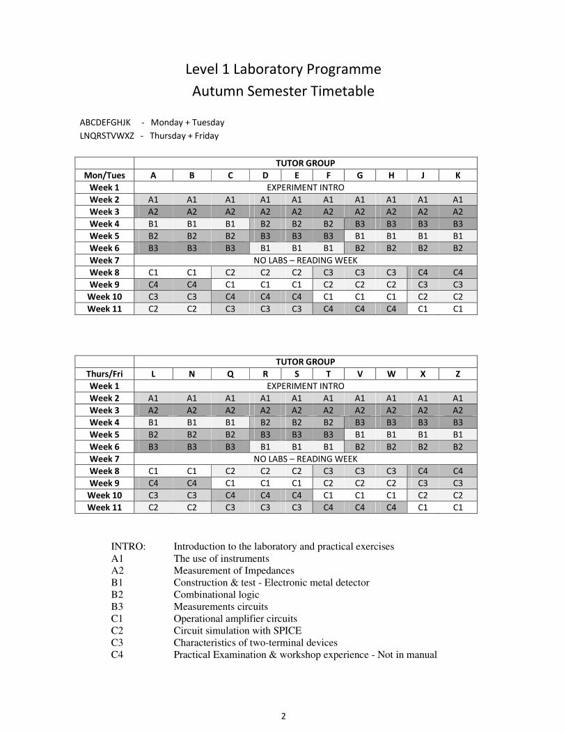
Level 1 Laboratory Programme
Autumn Semester Timetable
ABCDEFGHJK - Monday + Tuesday
LNQRSTVWXZ - Thursday + Friday
TUTOR GROUP
Mon/Tues A B C D E F G H J K
Week 1 EXPERIMENT INTRO
Week 2 A1 A1 A1 A1 A1 A1 A1 A1 A1 A1
Week 3 A2 A2 A2 A2 A2 A2 A2 A2 A2 A2
Week 4 B1 B1 B1 B2 B2 B2 B3 B3 B3 B3
Week 5 B2 B2 B2 B3 B3 B3 B1 B1 B1 B1
Week 6 B3 B3 B3 B1 B1 B1 B2 B2 B2 B2
Week 7 NO LABS – READING WEEK
Week 8 C1 C1 C2 C2 C2 C3 C3 C3 C4 C4
Week 9 C4 C4 C1 C1 C1 C2 C2 C2 C3 C3
Week 10 C3 C3 C4 C4 C4 C1 C1 C1 C2 C2
Week 11 C2 C2 C3 C3 C3 C4 C4 C4 C1 C1
TUTOR GROUP
Thurs/Fri L N Q R S T V W X Z
Week 1 EXPERIMENT INTRO
Week 2 A1 A1 A1 A1 A1 A1 A1 A1 A1 A1
Week 3 A2 A2 A2 A2 A2 A2 A2 A2 A2 A2
Week 4 B1 B1 B1 B2 B2 B2 B3 B3 B3 B3
Week 5 B2 B2 B2 B3 B3 B3 B1 B1 B1 B1
Week 6 B3 B3 B3 B1 B1 B1 B2 B2 B2 B2
Week 7 NO LABS – READING WEEK
Week 8 C1 C1 C2 C2 C2 C3 C3 C3 C4 C4
Week 9 C4 C4 C1 C1 C1 C2 C2 C2 C3 C3
Week 10 C3 C3 C4 C4 C4 C1 C1 C1 C2 C2
Week 11 C2 C2 C3 C3 C3 C4 C4 C4 C1 C1
INTRO: Introduction to the laboratory and practical exercises
A1 The use of instruments
A2 Measurement of Impedances
B1 Construction & test - Electronic metal detector
B2 Combinational logic
B3 Measurements circuits
C1 Operational amplifier circuits
C2 Circuit simulation with SPICE
C3 Characteristics of two-terminal devices
C4 Practical Examination & workshop experience - Not in manual

3
1. INTRODUCTION
1.1 Information about laboratory work
In the course of the year you will be issued with two sets of information about your laboratory
work. This, the first, sets out the organisation of the laboratory, has notes on various aspects of
experimental procedure, and gives details of the work you will undertake during the first
semester. A second set of online material, giving details of the experiments for the second
semester will be available on the ULearn system. You will also be given notes on the subject of
Safety. Further details and any modifications to the programme which may be necessary will be
posted in the first year laboratory (6 AB 04).
1.2 Purpose of laboratory work
Laboratory work serves many widely differing purposes and, though opinions may vary on the
relative value of these, the overall importance of the work is unquestioned. Among the objectives
are:
(i) To complement learning through lectures and textbooks. In many instances the
experiment will be scheduled to follow the lectures on the principal subject of the piece
of work. In others the sequence may be reversed, or there may be subsidiary topics which
you will not have encountered formally — much as occurs in any but the most routine
“real” engineering jobs — and which you will therefore have to study yourself.
(ii) To develop basic technical skills, using laboratory instruments and equipment,
constructing experimental circuits, making measurements and observations.
(iii) To encourage a professional approach to practical work, through adequate planning
and preparation, through learning to use effectively the limited time available, through
proper maintenance of useful and relevant notes (a log book), and through completion of
the work in a written report.
(iv) To encourage the development of higher engineering skills —definition of the
problem to be solved, synthesis of a solution, realisation of the solution and bringing it to
a successful conclusion.
Naturally the emphasis on each objective varies from one experiment to another. It is, however,
to be hoped that there is sufficient flexibility within most experiments for you to shift the
emphasis to suit your own needs. The laboratory staff will be pleased to discuss, and to
accommodate as far as possible, any reasonable variations.
4
2. LABORATORY ORGANISATION
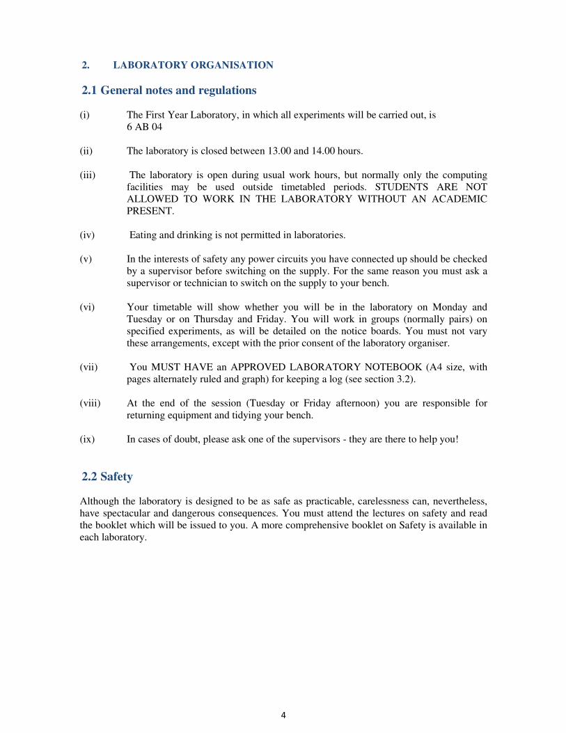
2.1 General notes and regulations
(i) The First Year Laboratory, in which all experiments will be carried out, is
6 AB 04
(ii) The laboratory is closed between 13.00 and 14.00 hours.
(iii) The laboratory is open during usual work hours, but normally only the computing
facilities may be used outside timetabled periods. STUDENTS ARE NOT
ALLOWED TO WORK IN THE LABORATORY WITHOUT AN ACADEMIC
PRESENT.
(iv) Eating and drinking is not permitted in laboratories.
(v) In the interests of safety any power circuits you have connected up should be checked
by a supervisor before switching on the supply. For the same reason you must ask a
supervisor or technician to switch on the supply to your bench.
(vi) Your timetable will show whether you will be in the laboratory on Monday and
Tuesday or on Thursday and Friday. You will work in groups (normally pairs) on
specified experiments, as will be detailed on the notice boards. You must not vary
these arrangements, except with the prior consent of the laboratory organiser.
(vii) You MUST HAVE an APPROVED LABORATORY NOTEBOOK (A4 size, with
pages alternately ruled and graph) for keeping a log (see section 3.2).
(viii) At the end of the session (Tuesday or Friday afternoon) you are responsible for
returning equipment and tidying your bench.
(ix) In cases of doubt, please ask one of the supervisors - they are there to help you!
2.2 Safety
Although the laboratory is designed to be as safe as practicable, carelessness can, nevertheless,
have spectacular and dangerous consequences. You must attend the lectures on safety and read
the booklet which will be issued to you. A more comprehensive booklet on Safety is available in
each laboratory.
5
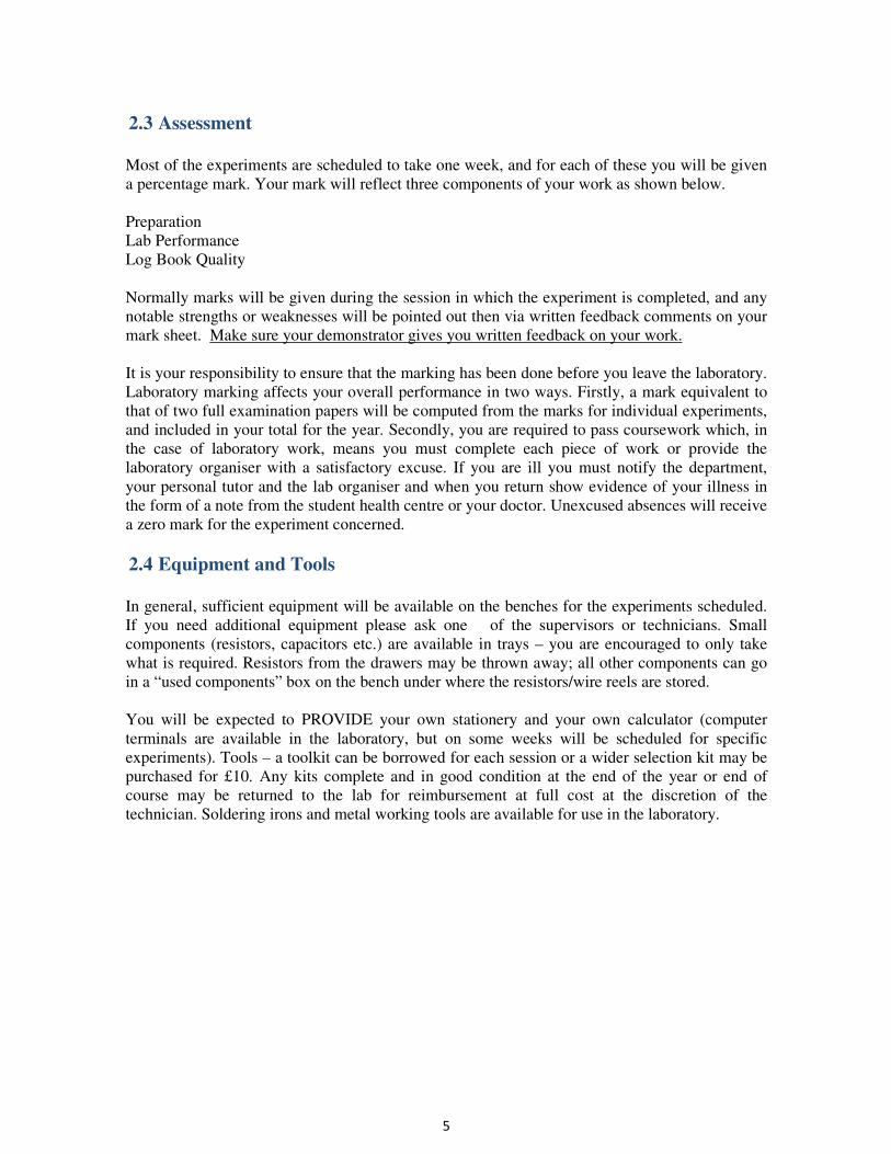
2.3 Assessment
Most of the experiments are scheduled to take one week, and for each of these you will be given
a percentage mark. Your mark will reflect three components of your work as shown below.
Preparation
Lab Performance
Log Book Quality
Normally marks will be given during the session in which the experiment is completed, and any
notable strengths or weaknesses will be pointed out then via written feedback comments on your
mark sheet. Make sure your demonstrator gives you written feedback on your work.
It is your responsibility to ensure that the marking has been done before you leave the laboratory.
Laboratory marking affects your overall performance in two ways. Firstly, a mark equivalent to
that of two full examination papers will be computed from the marks for individual experiments,
and included in your total for the year. Secondly, you are required to pass coursework which, in
the case of laboratory work, means you must complete each piece of work or provide the
laboratory organiser with a satisfactory excuse. If you are ill you must notify the department,
your personal tutor and the lab organiser and when you return show evidence of your illness in
the form of a note from the student health centre or your doctor. Unexcused absences will receive
a zero mark for the experiment concerned.
2.4 Equipment and Tools
In general, sufficient equipment will be available on the benches for the experiments scheduled.
If you need additional equipment please ask one of the supervisors or technicians. Small
components (resistors, capacitors etc.) are available in trays – you are encouraged to only take
what is required. Resistors from the drawers may be thrown away; all other components can go
in a “used components” box on the bench under where the resistors/wire reels are stored.
You will be expected to PROVIDE your own stationery and your own calculator (computer
terminals are available in the laboratory, but on some weeks will be scheduled for specific
experiments). Tools – a toolkit can be borrowed for each session or a wider selection kit may be
purchased for £10. Any kits complete and in good condition at the end of the year or end of
course may be returned to the lab for reimbursement at full cost at the discretion of the
technician. Soldering irons and metal working tools are available for use in the laboratory.
6
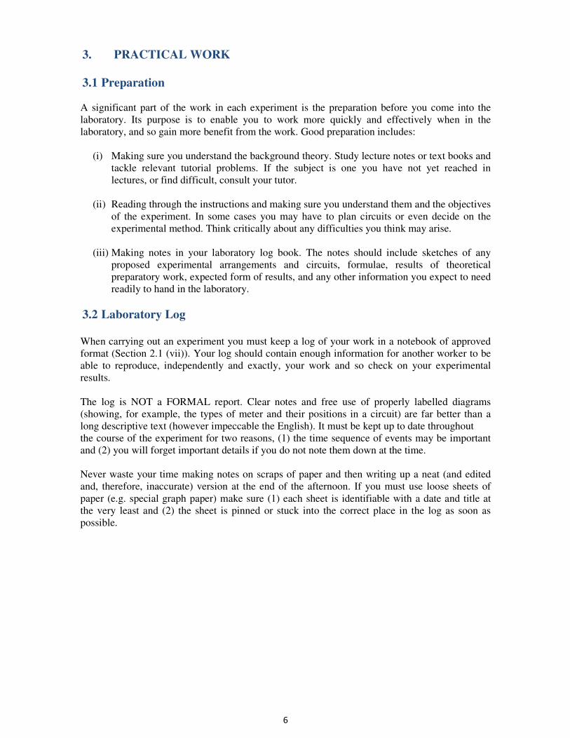
3. PRACTICAL WORK
3.1 Preparation
A significant part of the work in each experiment is the preparation before you come into the
laboratory. Its purpose is to enable you to work more quickly and effectively when in the
laboratory, and so gain more benefit from the work. Good preparation includes:
(i) Making sure you understand the background theory. Study lecture notes or text books and
tackle relevant tutorial problems. If the subject is one you have not yet reached in
lectures, or find difficult, consult your tutor.
(ii) Reading through the instructions and making sure you understand them and the objectives
of the experiment. In some cases you may have to plan circuits or even decide on the
experimental method. Think critically about any difficulties you think may arise.
(iii) Making notes in your laboratory log book. The notes should include sketches of any
proposed experimental arrangements and circuits, formulae, results of theoretical
preparatory work, expected form of results, and any other information you expect to need
readily to hand in the laboratory.
3.2 Laboratory Log
When carrying out an experiment you must keep a log of your work in a notebook of approved
format (Section 2.1 (vii)). Your log should contain enough information for another worker to be
able to reproduce, independently and exactly, your work and so check on your experimental
results.
The log is NOT a FORMAL report. Clear notes and free use of properly labelled diagrams
(showing, for example, the types of meter and their positions in a circuit) are far better than a
long descriptive text (however impeccable the English). It must be kept up to date throughout
the course of the experiment for two reasons, (1) the time sequence of events may be important
and (2) you will forget important details if you do not note them down at the time.
Never waste your time making notes on scraps of paper and then writing up a neat (and edited
and, therefore, inaccurate) version at the end of the afternoon. If you must use loose sheets of
paper (e.g. special graph paper) make sure (1) each sheet is identifiable with a date and title at
the very least and (2) the sheet is pinned or stuck into the correct place in the log as soon as
possible.

7
Listed below are most of the important features of a good log:
(i) Title and date of experiment.
(ii) Object of experiment, if not clear from the title.
(iii) Preliminary notes, properly labelled or numbered for easy reference.
(iv) List of equipment, with type and serial number if relevant.
(v) Circuit diagrams and notes on experimental details, mistakes made, and observations which
would help anyone repeating the experiment.
(vi) Readings, exactly as taken from instruments and in tabular form if appropriate, with notes on
uncertainties, range changes on meters, etc.
(vii) Headings and section numbers to allow easy reference.
(viii) Data processing - this may be by calculation or by graph, and should be carried out in the
course of the experiment so that readings which need extending or repeating become obvious
immediately. Note also that any manipulation of a reading (even just scaling to accommodate
non-standard ranges on instruments) should be shown.
(ix) Proper labelling of graphs.
(x) Calculations yielding an estimate of the accuracy of the numerical results.
(xi) A summary of results, and any comments and conclusions that can be reached in the time
available.
3.3 Procedure
For most of the first year experiments the procedure will appear to be fairly clearly set out in the
instructions. Do not, however, be misled into following these without thinking, for the finer
points which distinguish a good piece of work from the average or poor are not generally
detailed.
Before you start to take readings, think about how you will record and process the data. In most
cases a graph will be the most useful way of presenting results; often it will be best to use log
scaled paper, or to plot the log, or other function, of the data. If possible, make and record a few
preliminary readings with widely spaced values to try and establish areas of interest; the details
can be filled in afterwards. Record readings (or results as appropriate) as they are obtained —
this should ensure doubtful points are checked, allow unnecessarily frequent readings to be
avoided and generally improve experimental technique.
Remember that the instructions are intended only as a guide. We want to encourage any initiative
which will lead to the experiments being more useful, interesting and enjoyable. The only
restrictions will be set by availability of equipment and by safety considerations (in particular, all
power circuits should be checked by a supervisor before switching on).
8
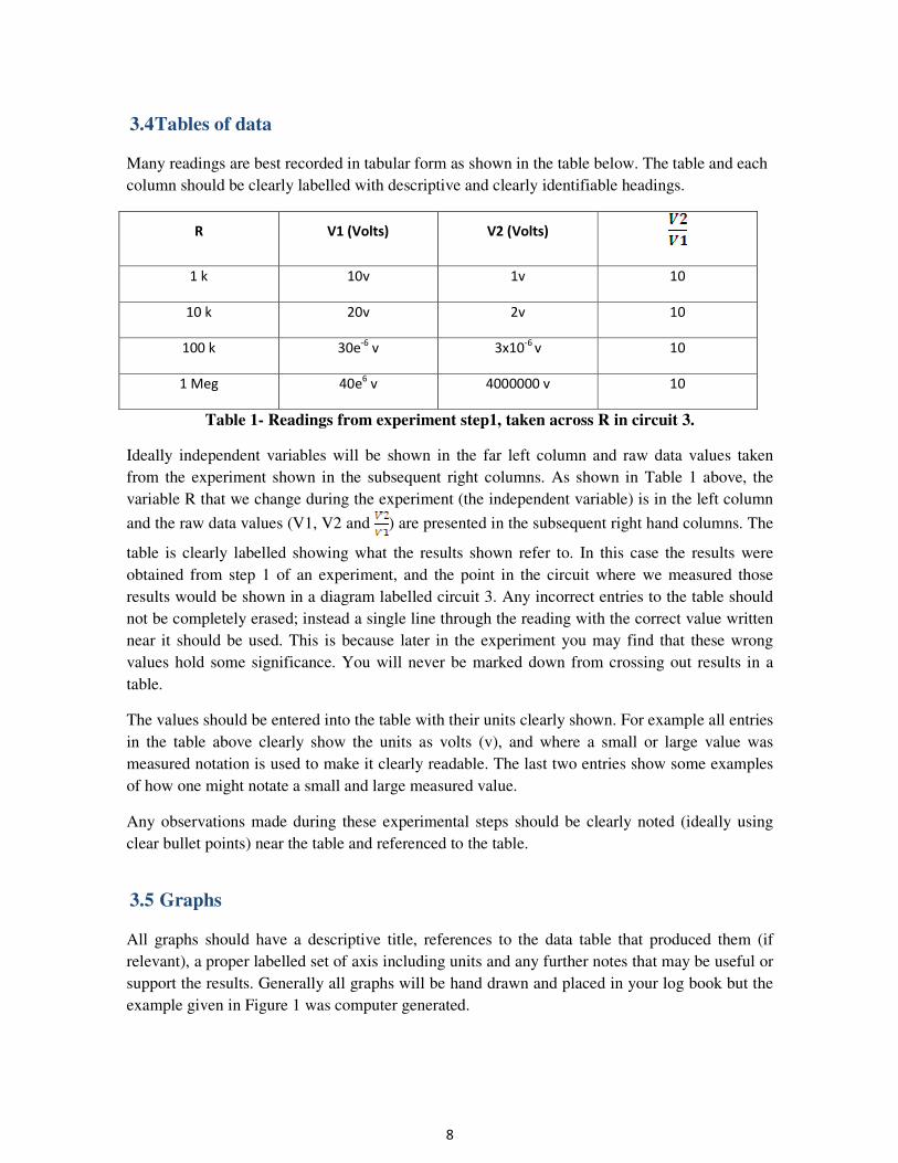
3.4 Tables of data
Many readings are best recorded in tabular form as shown in the table below. The table and each
column should be clearly labelled with descriptive and clearly identifiable headings.
R V1 (Volts) V2 (Volts)
1 k 10v 1v 10
10 k 20v 2v 10
100 k 30e-6
v 3x10⁻⁶
v 10
1 Meg 40e6 v 4000000 v 10
Table 1- Readings from experiment step1, taken across R in circuit 3.
Ideally independent variables will be shown in the far left column and raw data values taken
from the experiment shown in the subsequent right columns. As shown in Table 1 above, the
variable R that we change during the experiment (the independent variable) is in the left column
and the raw data values (V1, V2 and ) are presented in the subsequent right hand columns. The
table is clearly labelled showing what the results shown refer to. In this case the results were
obtained from step 1 of an experiment, and the point in the circuit where we measured those
results would be shown in a diagram labelled circuit 3. Any incorrect entries to the table should
not be completely erased; instead a single line through the reading with the correct value written
near it should be used. This is because later in the experiment you may find that these wrong
values hold some significance. You will never be marked down from crossing out results in a
table.
The values should be entered into the table with their units clearly shown. For example all entries
in the table above clearly show the units as volts (v), and where a small or large value was
measured notation is used to make it clearly readable. The last two entries show some examples
of how one might notate a small and large measured value.
Any observations made during these experimental steps should be clearly noted (ideally using
clear bullet points) near the table and referenced to the table.
3.5 Graphs
All graphs should have a descriptive title, references to the data table that produced them (if
relevant), a proper labelled set of axis including units and any further notes that may be useful or
support the results. Generally all graphs will be hand drawn and placed in your log book but the
example given in Figure 1 was computer generated.
9
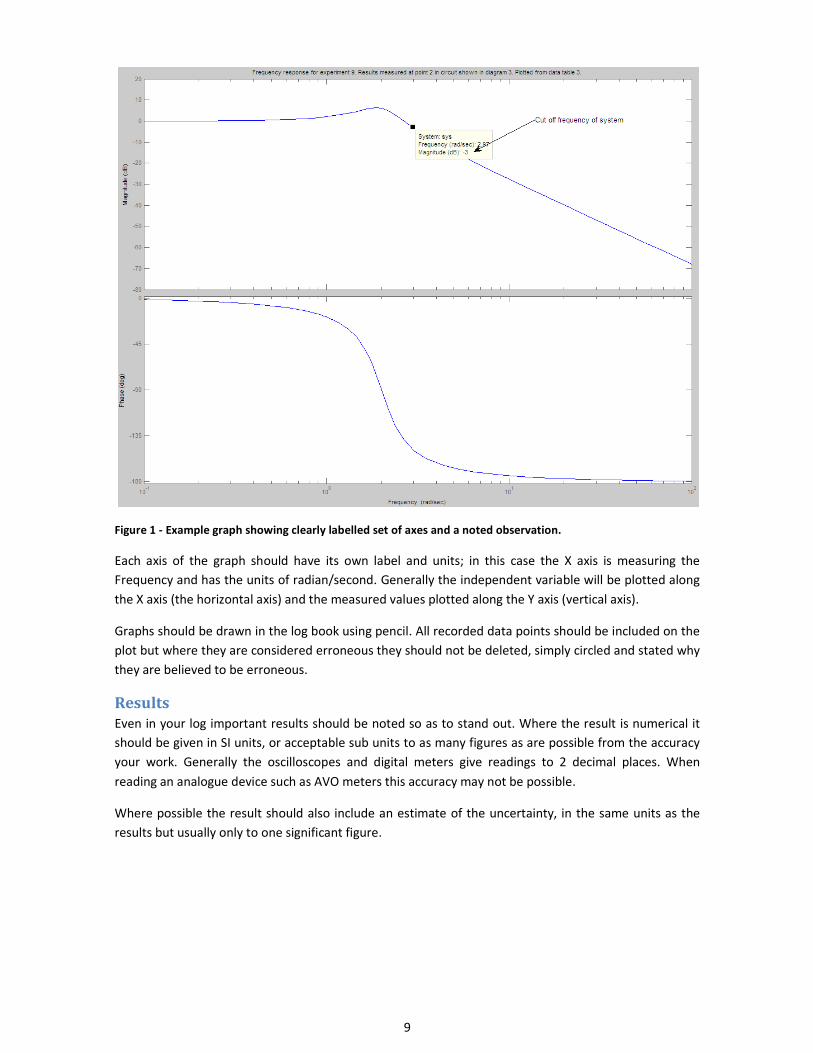
Figure 1 - Example graph showing clearly labelled set of axes and a noted observation.
Each axis of the graph should have its own label and units; in this case the X axis is measuring the
Frequency and has the units of radian/second. Generally the independent variable will be plotted along
the X axis (the horizontal axis) and the measured values plotted along the Y axis (vertical axis).
Graphs should be drawn in the log book using pencil. All recorded data points should be included on the
plot but where they are considered erroneous they should not be deleted, simply circled and stated why
they are believed to be erroneous.
Results
Even in your log important results should be noted so as to stand out. Where the result is numerical it
should be given in SI units, or acceptable sub units to as many figures as are possible from the accuracy
your work. Generally the oscilloscopes and digital meters give readings to 2 decimal places. When
reading an analogue device such as AVO meters this accuracy may not be possible.
Where possible the result should also include an estimate of the uncertainty, in the same units as the
results but usually only to one significant figure.

10
4 Experiments
Experiment: Intro
Welcome to your first day in the EE labs!
The aim of this un-assessed “experiment” is to familiarise you with the facilities, equipment and
techniques in the undergraduate laboratories in a more structured way, separate from the formal
lab work.
This experiment will be split over two days. During the first day the group will be split into 5
groups based on tutorial groups and will visit each of 5 stations for a demonstration given by the
3 PhD demonstrators and 2 lab academics. Each ~20 min demonstration will introduce a specific
set of basic knowledge important for future lab work. Some of the sessions will include hands-on
elements to aid learning. The second day will allow you to practice what you have learnt the
previous day by performing two simple practical exercises under supervision.
Day 1
Station 1: Components, Connections and Lab Tidiness
Introduction to the components and facilities available in the laboratory and the relevant health
and safety issues. Activities to include reading resistor values, identifying capacitors (inc.
Electrolytic) and diodes, introduction to IC packages – particularly op-amps and explanation of
the internal structure of BNC cables.
Station 2: Breadboards and Veroboard
Careful practical explanation of the connections inside breadboard (often a source of confusion)
and hints and tips on how to structure and organise a circuit (inc. colour coding wires).
Introduction to veroboard.
Station 3: Soldering
Practical demonstration plus some limited hands on practice before the exercise on day 2.
Soldering handout to be given to students.
Station 4: Oscilloscopes
How the oscilloscope works – especially common nature of ground connections and the
consequences for measurements. Concept of triggering. Common “problems” with setting up
oscilloscope. CROs vs digital scopes.
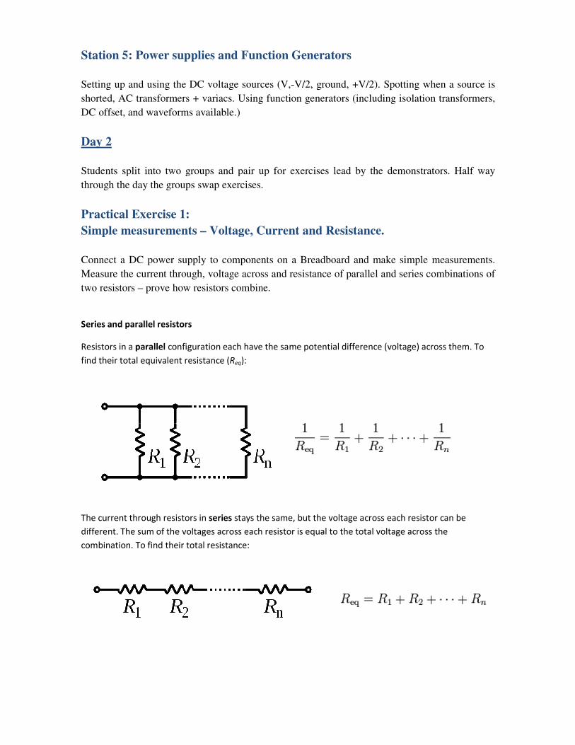
Station 5: Power supplies and Function Generators
Setting up and using the DC voltage sources (V,
shorted, AC transformers + variacs. Using function generators (including isolation transformers,
DC offset, and waveforms available.)
Day 2
Students split into two groups and pair up for exercises
through the day the groups swap exercises
Practical Exercise 1:
Simple measurements – Voltage, Current and Resistance.
Connect a DC power supply to components on a Breadboard and make simple measurements.
Measure the current through, voltage a
two resistors – prove how resistors combine.
Series and parallel resistors
Resistors in a parallel configuration each have the same potential difference (voltage)
find their total equivalent resistance (
The current through resistors in series
different. The sum of the voltages across each resistor
combination. To find their total resistance:
Station 5: Power supplies and Function Generators
Setting up and using the DC voltage sources (V,-V/2, ground, +V/2). Spotting when a source is
AC transformers + variacs. Using function generators (including isolation transformers,
DC offset, and waveforms available.)
Students split into two groups and pair up for exercises lead by the demonstrators
exercises.
Voltage, Current and Resistance.
Connect a DC power supply to components on a Breadboard and make simple measurements.
Measure the current through, voltage across and resistance of parallel and series combinations of
prove how resistors combine.
configuration each have the same potential difference (voltage) across them
equivalent resistance (Req):
series stays the same, but the voltage across each resistor can be
voltages across each resistor is equal to the total voltage across the
their total resistance:
otting when a source is
AC transformers + variacs. Using function generators (including isolation transformers,
lead by the demonstrators. Half way
Connect a DC power supply to components on a Breadboard and make simple measurements.
cross and resistance of parallel and series combinations of
across them. To
stays the same, but the voltage across each resistor can be
across the
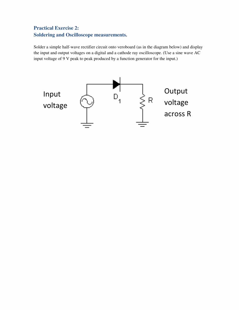
Practical Exercise 2:
Soldering and Oscilloscope measurements.
Solder a simple half-wave rectifier circuit onto veroboard (as in the diagram below) and display
the input and output voltages on a digital and a cathode ray oscilloscope. (Use a sine wave AC
input voltage of 9 V peak to peak produced by a function generator for the input.)
Input
voltage
Output
voltage
across R
13
The Use of Instruments (Experiment A1)
1. Aim
The major aim of this experiment is to introduce you to some of the instruments and
equipment commonly used in electronic and electrical engineering laboratories.
Even though you may have met some of the equipment before, you should carry out
the experiment as indicated in order to refresh or confirm your knowledge. An
important aspect of the experiment is that it will illustrate some of the limitations of
the instruments and help you to develop good measurement techniques. This is
essential if you wish to be successful when you carry out more demanding
experiments, later in the course.
A secondary aim of the experiment is to give you guidance on how to keep a log
book. For all subsequent experiments, you will be required to keep a log as
described in Section 3.2 of the Preliminary Notes. For this experiment you should
fill in data and add comments, as requested, directly onto the instruction sheet, which
will then be a model for future work.
2. Introduction
Instruments make correct measurements only within specified limits, usually of
frequency, amplitude and waveform. Thus, before using an instrument with which
you are unfamiliar, to measure some particular quantity, it is necessary to consult the
manual to ascertain that the instrument is capable of measuring correctly, the quantity
in question. But this is not sufficient; all instruments disturb, to some extent, the
circuit to which they are connected. For example, if a voltmeter of low resistance is
used to measure the voltage distribution in a network of high resistances, the
application of the voltmeter between any two points will completely upset the current
distribution in the network. The meter is said to ‘load’ the circuit. Note that the
meter does not, in this case, indicate the ‘wrong’ voltage, if it is operating within its
correct frequency range etc. As mentioned earlier it will correctly indicate the
voltage difference between its terminals, but the voltage between the points in the
circuit with the meter connected is not the same as it was before the meter was
applied. Ideally, the meter loading should be negligible and it is essential to check,
before using an instrument, whether it will load the circuit. If it puts a significant
load on the circuit, it may still be possible to use the instrument provided that a
suitable allowance is made.
It is assumed that you have some understanding of the basic principles upon which
instruments such as the analogue AVO and oscilloscope are based. If this is not the
case, you should consult the instrument manuals in the laboratory or a suitable
textbook.
3. Experimental Work
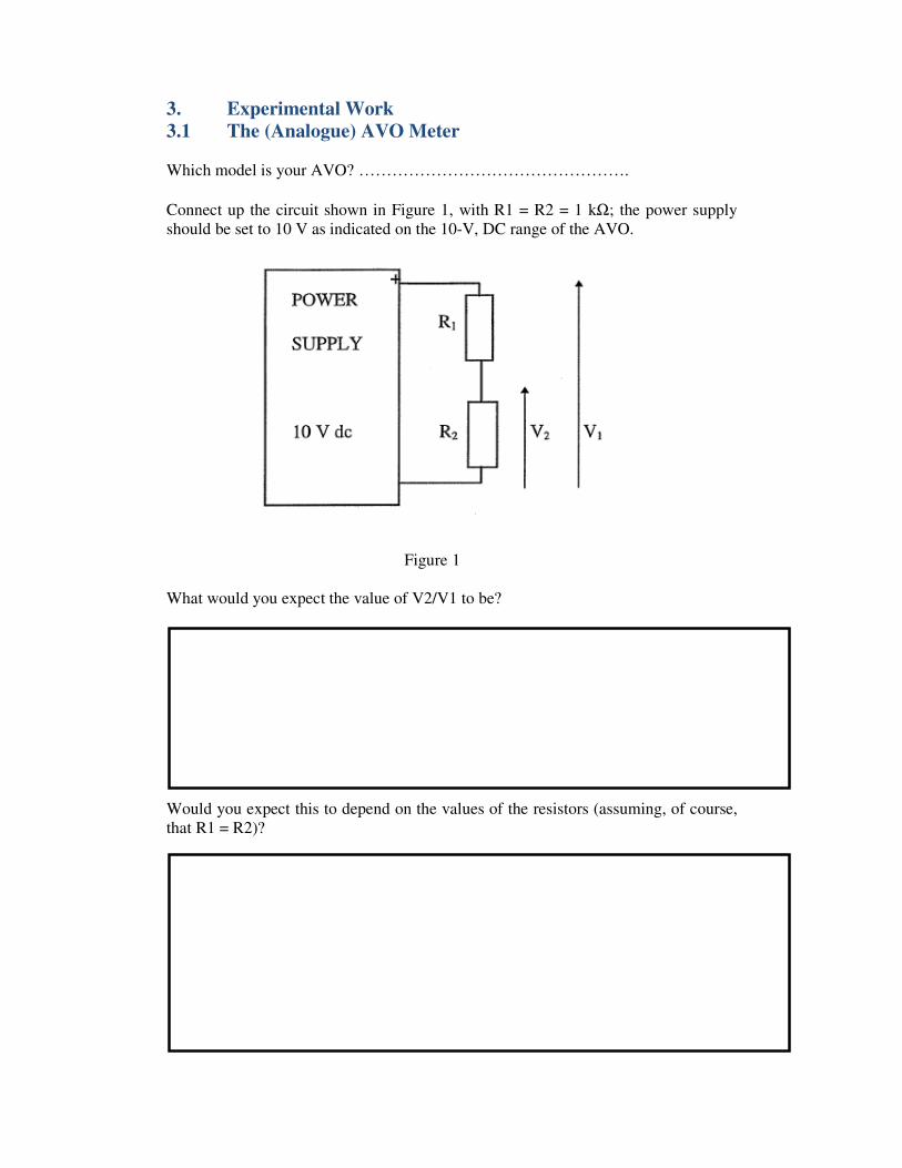
3.1 The (Analogue) AVO Meter
Which model is your AVO? ………………………………………….
Connect up the circuit shown in Figure 1, with R1 = R2 = 1 kΩ; the power supply
should be set to 10 V as indicated on the 10-V, DC range of the AVO.
Figure 1
What would you expect the value of V2/V1 to be?
Would you expect this to depend on the values of the resistors (assuming, of course,
that R1 = R2)?

15
Using the AVO meter, measure V1 and V2, and determine the ratio V2/V1. Repeat
the measurement for the following resistor values:
R1 = R2 = 10 kΩ, 100 kΩ, 1 MΩ
R1 = R2 (Ω)
V1(Volts)
V2(Volts)
V2/V1
1 k
10 k
100 k
1 M
Table 1
Explain the general trend of V2/V1 as the resistance value increases and using any one of
the results, calculate what you can about the resistance of the AVO.
Having carried out the calculation do you think that you chose the most appropriate result
(1 k, 10 k, 100 k or 1 M)? If not, repeat your calculation.
The AVO sensitivity on DC ranges is quoted at 20 kΩ/V. Can you reconcile this with the
value you have deduced? What does it tell you about the maximum value of the DC
current through the meter for full-scale deflection (FSD)?

16
3.2 The Digital Multimeter for DC voltage measurement
The digital multimeter uses an analogue-to-digital conversion circuit that samples the input
and converts it to a reading. Repeat the experiment given in Section 3.1, using the digital
multimeter (on the 20-V, DC range) to measure V1 and V2.
R1 = R2 (Ω)
V1(V)
V2(V)
V2/V1
1 k
10 k
100 k
1 M
Table 2
Compare the values of V2/V1 with those obtained previously, and explain the difference.
Can you estimate, from any of the previous results, the input resistance of the multimeter?
If so, make an estimate and compare your result with that quoted for the instrument (see
the back of the instrument). If not, explain why you cannot.
Make brief notes on what you regard as the relative merits of the two instruments, bearing
in mind that you have only been studying some of their capabilities.
What can you conclude about the impedance requirements of a voltmeter which is to be
used for measuring voltage in a particular circuit?

17
3.3 The Oscilloscope
READ THIS SECTION CAREFULLY. The oscilloscope is probably the most versatile
of all electronic instruments. In the labs we have both digital and cathode ray
oscilloscopes (CRO). In this section the operation of the CRO will be explained, but you are encouraged to use both digital scopes and CROs in later experiments. The
CRO is a fast response, two dimensional graph plotter and it is most often used for
observing, and if necessary making quantitative measurements of, voltage as a function of
time. T This is the mode in which it is to be used in this experiment. In later experiments,
you will use the CRO to display one voltage as a function of another (the so-called X-Y
mode). There are several CROs in this laboratory; all have similar specifications. The first
thing to do is to familiarise yourself with the basic controls and set up the CRO so as to
obtain a stable image.
Producing a stable trace is relatively easy on modern CROs, but it is important to
appreciate the principles by which it is achieved. Firstly, you will realise that the trace
produced by a single traversal of the screen, by the spot, will not result in a visible,
stationary picture. This is obtained only when the trace is reinforced by repeated
superposition of the waveform. This obviously requires that the waveform be periodic. It
is also necessary for each successive trace the start at the same point in its cycle.
The time base circuit is designed so that it requires a trigger signal before it can start.
When it receives this signal the time base produces a ramp voltage, large enough to drive
the spot from the left to the right of the screen. The ramp voltage then falls quickly to zero
so that the spot completes its cycle with a ‘fly-back’. The spot then waits for the next
trigger signal before repeating the process.
Triggering is controlled by selecting a trigger mode and the trigger level. The signal from
which the trigger is obtained can be the waveform applied to channel I, channel II or a
quite different, ‘external’, signal. In the ‘AUTO’ position, a stable display is obtained for
almost any waveform. If the signal has insufficient amplitude or pulse repetition rate, a
free running reference trace will appear. In the ‘NORM’ position, the ‘LEVEL’ control
can be adjusted to provide triggering from any part of the leading edge of the displayed
signal. When ‘TV’ is selected, a low-pass filter is introduced into the trigger circuit to
assist triggering from a modulated signal (see below) and to prevent triggering by the high
frequency carrier; in this mode the ‘LEVEL’ control is inoperative.
Set the controls initially as indicated below (HAMEG HM203 given here):
POWER OFF (OUT) VAR TIME CAL
INTENS CENTRAL COMPONENT TESTER OUT
FOCUS CENTRAL CH I
X-Y OUT VOLTS/DIV 1 V
VAR CAL
XMAG OUT Y POS.I CENTRAL
COUPLING DC
X-POS CENTRAL CH II
TRIG VOLTS/DIV 1 V
SELECTOR AC VAR CAL
Y POS.II CENTRAL
EXT OUT COUPLING DC
SLOPE +(OUT) INV OUT
AT/NORM OUT CHI/II OUT
TIME/DIV 2 ms DUAL OUT
18
Now switch on. If a trace does not appear in a short while, consult a supervisor. Centralise
the trace using the relevant X and Y controls. Adjust the ‘INTENSITY’ until the trace is at
a suitable viewing intensity and adjust the ‘FOCUS’ for best overall definition. Adjust the
‘Y POS.I’ control to bring the trace level with the centre graticule line.
3.4 Measurement of AC Waveforms
(a) Using a function generator, connect a 1-kHz input signal of approximately 4 V, peak-
to-peak to the ‘CH I’ input socket and make any necessary adjustments to obtain a suitable
trace. Sketch1 the waveform. Measure the amplitude (pk-pk) of the wave and its
frequency with the CRO and compare them with the oscillator settings. Note that the time
base sweep speeds are only as indicated on the panel markings when the ‘XMAG’ control
is out, for x1 gain, and the variable speed control is at the ‘CAL’ position.
Oscillator setting:
Amplitude ………. V Frequency ………. Hz
CRO measurement:
Amplitude ………. V Frequency ………. Hz
(b) With the Y-amplifier set to 1 V, observe the effect of varying the ‘LEVEL’ control.
Set the trigger mode to ‘NORM’ and once again observe the effect of varying the ‘LEVEL’
control. Is there any difference?
(c) Operate the ± trigger level and confirm that the instant in the cycle at which triggering
occurs, changes by half a cycle for sine waves.
(d) Set the Y-amplifier to a few other sensitivities and the sweep speed to several other
positions and confirm that the trace changes as you would expect.
(e) Set the function generator to 5V peak-to-peak 1kHz sine wave and adjust the CRO to
display the trace clearly. Set the AVO to measure AC voltage and connect it in parallel
with the CRO across the output of the function generator.
1 “Sketch” means a rough drawing depicting the essential features of the waveform together with a clear indication
of the X- and Y-scales.
19
Make a sketch of the setup noting the polarities.
Compare the peak-to-peak voltages measured on the AVO and the CRO. Explain any
difference.
(c) Check the operation of the DC offset control on the function generator. This control
allows us to add a fixed (DC) voltage to the AC output of the function generator. Set the
peak-to-peak voltage of the function generator to 4V and setup the CRO to clearly show
the trace. Now increase the DC offset to its maximum. The trace may now have
vanished. How could we set up the CRO to display the trace in this case?

20
3.5 The Frequency Response of the AVO and DVM
Set the function generator (no offset) to 1 kHz and 5 V (as measured by the AVO on the
10-V range). Add the DVM in parallel with the AVO and note the DVM reading. Given
the accuracy of ±2% FSD for the AVO on AC ranges and ±1% of reading, ±2 digits for the
DVM on the 20-V, AC range, do the meters agree?
(a) Increase the frequency to 10 kHz and note the AVO reading and note the frequencies at
which the AVO reading has dropped by 2% (to 4.9 V) and 5% (to 4.5 V). Check the
CRO to ensure that the oscillator voltage has not changed. The specification for the
AVO is ±3% up to 15 kHz. Does it meet the specification?
The specification for the AVO is ±3% up to 15 kHz. Does it meet the specification?
(b) Repeat the experiment with the DVM, noting the frequencies at which the reading is
2% down and 5% down. Compare your answers with the specification, as given in the
instruction booklet (available from lab technician.)
21
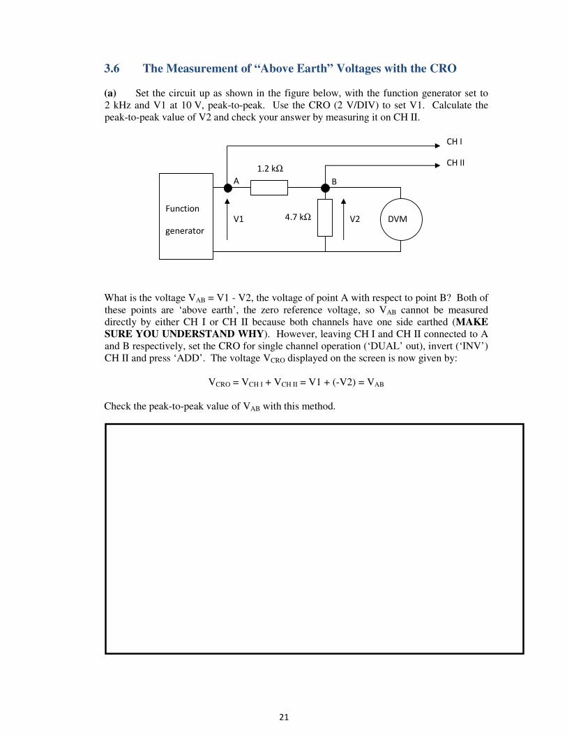
3.6 The Measurement of “Above Earth” Voltages with the CRO
(a) Set the circuit up as shown in the figure below, with the function generator set to
2 kHz and V1 at 10 V, peak-to-peak. Use the CRO (2 V/DIV) to set V1. Calculate the
peak-to-peak value of V2 and check your answer by measuring it on CH II.
What is the voltage VAB = V1 - V2, the voltage of point A with respect to point B? Both of
these points are ‘above earth’, the zero reference voltage, so VAB cannot be measured
directly by either CH I or CH II because both channels have one side earthed (MAKE
SURE YOU UNDERSTAND WHY). However, leaving CH I and CH II connected to A
and B respectively, set the CRO for single channel operation (‘DUAL’ out), invert (‘INV’)
CH II and press ‘ADD’. The voltage VCRO displayed on the screen is now given by:
VCRO = VCH I + VCH II = V1 + (-V2) = VAB
Check the peak-to-peak value of VAB with this method.
Function
generator
DVM
1.2 kΩ
4.7 kΩ
CH I
CH II
V1 V2
A B

22
3.7 Measuring phase differences
Set the circuit up as shown in the figure below, with the function generator set to 5 V,
peak-to-peak. Measure V1 and V2 for a range of frequencies from 1kHz to 10 kHz.
.
As you vary the frequency observe how the phase angle between V1 and V2 varies. What
does this tell you? (N.B. This leads on to the concept of impedance in experiment A2.)
B H Venning (revised 2011 S Henley)
Function
generator
10nF
4.7 kΩ
CH I
CH II
V1 V2
A B
23
Measurement of Impedances (Experiment A2)
This experiment is in four parts (1,2,3 and 4) you should do all of them.
Part 1 : Ohm’s Law for Resistors
Aims
1) To verify Ohms Law, V=IR. The voltage V developed across a resistor R is
proportional to the product of the current I flowing through the resistor and the
value R of the resistor.
2) To discover the problems using measuring equipment such as an oscilloscope,
that has two inputs which have a common connection.
3) To observe the effect on the output voltage of a device (power supply or signal
generator) when appreciable current is drawn from the device.
4) To learn the significance of d.c. coupling to an oscilloscope input.
5) To learn to ensure that the variable gain amplifiers of a oscilloscope are set in the
calibrated position before trying to take accurate measurements.
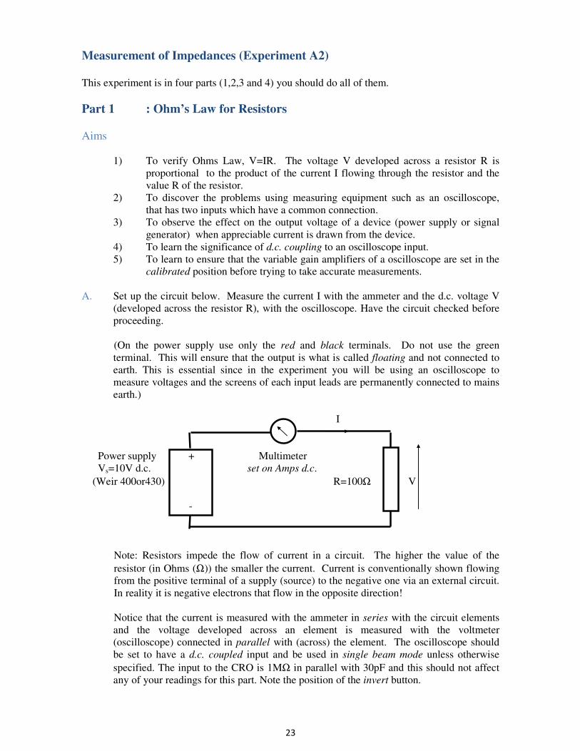
A. Set up the circuit below. Measure the current I with the ammeter and the d.c. voltage V
(developed across the resistor R), with the oscilloscope. Have the circuit checked before
proceeding.
(On the power supply use only the red and black terminals. Do not use the green
terminal. This will ensure that the output is what is called floating and not connected to
earth. This is essential since in the experiment you will be using an oscilloscope to
measure voltages and the screens of each input leads are permanently connected to mains
earth.)
I
Power supply + Multimeter
Vs=10V d.c. set on Amps d.c.
(Weir 400or430) R=100Ω V
-
Note: Resistors impede the flow of current in a circuit. The higher the value of the
resistor (in Ohms (Ω)) the smaller the current. Current is conventionally shown flowing
from the positive terminal of a supply (source) to the negative one via an external circuit.
In reality it is negative electrons that flow in the opposite direction!
Notice that the current is measured with the ammeter in series with the circuit elements
and the voltage developed across an element is measured with the voltmeter
(oscilloscope) connected in parallel with (across) the element. The oscilloscope should
be set to have a d.c. coupled input and be used in single beam mode unless otherwise
specified. The input to the CRO is 1MΩ in parallel with 30pF and this should not affect
any of your readings for this part. Note the position of the invert button.
24
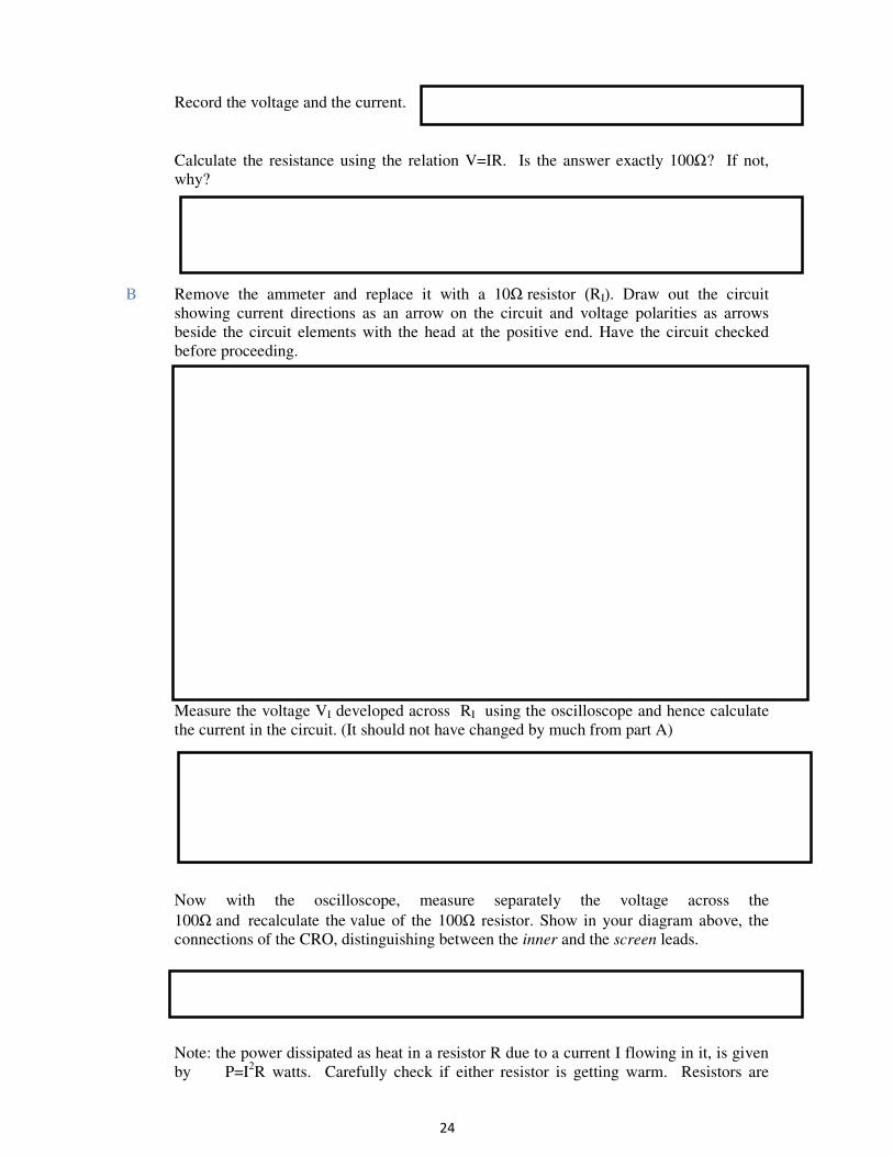
Record the voltage and the current.
Calculate the resistance using the relation V=IR. Is the answer exactly 100Ω? If not,
why?
B Remove the ammeter and replace it with a 10Ω resistor (RI). Draw out the circuit
showing current directions as an arrow on the circuit and voltage polarities as arrows
beside the circuit elements with the head at the positive end. Have the circuit checked
before proceeding.
Measure the voltage VI developed across RI using the oscilloscope and hence calculate
the current in the circuit. (It should not have changed by much from part A)
Now with the oscilloscope, measure separately the voltage across the
100Ω and recalculate the value of the 100Ω resistor. Show in your diagram above, the
connections of the CRO, distinguishing between the inner and the screen leads.
Note: the power dissipated as heat in a resistor R due to a current I flowing in it, is given
by P=I2R watts. Carefully check if either resistor is getting warm. Resistors are

25
produced with a specified power rating and normally should not be used outside their
rated value.
COMMENTS:
C Change the oscilloscope to dual beam mode and measure both voltages at the same time
but firstly draw a diagram to show the exact connections of the oscilloscope to the circuit,
in particular the connection of the screen lead which is common to both inputs (It is also
connected to mains earth through the oscilloscope case) Mark on your circuit diagram,
the direction of the current and the polarities of all the voltages. Note the position of the
invert button on both inputs to the oscilloscope. Check that you get the same value for the
resistor.
26
D Replace the d.c. supply with the sinusoidal ac voltage source (oscillator) set to ω=104
radians/sec. (ω=2πf, where f is the frequency in Hertz (Hz)). Remove RI and replace
with the current meter as in A but set to read amps a.c. Set the oscillator to give an
output voltage of about 1volt peak to peak (Vp-p). Check this with the oscilloscope on
single beam, and calculate the root mean square (r.m.s) value of this voltage. (mean
square (the square of r.m.s) =V2p/2 for a sine wave). Note how the output voltage of the
oscillator falls slightly when the circuit is connected. Do not bother to readjust it! (The
oscillator has a transformer on its output so that the output is floating)
Draw a diagram and repeat section A using the current meter on the a.c. current range.
Calculate the resistance at this frequency. Explain the reason why the output voltage of
the oscillator falls when the circuit is connected.
27
E Replace the current meter with the 10Ω current monitoring resistor as in B and observe
both voltages with the oscilloscope in dual beam mode at ω=104 rad/s. Sketch the
sinusoidal voltage roughly to scale in below, showing their relative phases. Remember to
allow for the polarity of the connections. (check and note the position of the invert
buttons on the inputs to the oscilloscope). Recalculate the value of the 100Ω resistor.
You may use the x pos control to align the trace on the oscilloscope.
F If your supervisor feels you have sufficient time then decide if you could repeat E if the
oscillator has one output terminal that is permanently connected to earth. Draw a
diagram to verify your answer.
28
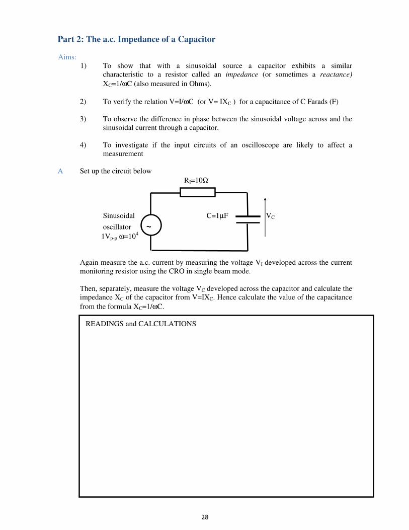
Part 2: The a.c. Impedance of a Capacitor
Aims:
1) To show that with a sinusoidal source a capacitor exhibits a similar
characteristic to a resistor called an impedance (or sometimes a reactance)
XC=1/ωC (also measured in Ohms).
2) To verify the relation V=I/ωC (or V= IXC ) for a capacitance of C Farads (F)
3) To observe the difference in phase between the sinusoidal voltage across and the
sinusoidal current through a capacitor.
4) To investigate if the input circuits of an oscilloscope are likely to affect a
measurement
A Set up the circuit below
RI=10Ω
Sinusoidal C=1µF VC
oscillator ~
1Vp-p ω=104
Again measure the a.c. current by measuring the voltage VI developed across the current
monitoring resistor using the CRO in single beam mode.
Then, separately, measure the voltage VC developed across the capacitor and calculate the
impedance XC of the capacitor from V=IXC. Hence calculate the value of the capacitance
from the formula XC=1/ωC.
READINGS and CALCULATIONS

29
B Now measure both voltages using the oscilloscope in dual beam mode and sketch the
waveforms showing their relative phases (allowing for the polarity of the connections).
Remember to add a scale to the diagram. Remember that the current is in phase with the
voltage across the monitoring resistor.
Draw a phasor diagram for the voltages and current (ask your demonstrator or an
academic to explain the concept of phasors at this point). To do this, draw a line along
the x axis to represent the peak value of the current. Then draw a line along the -y axis to
represent the magnitude of the peak value of the voltage across the capacitor. Then using
the same scaling draw a line to represent the magnitude of the peak voltage across the
resistor RI. Draw in the line representing the source voltage VS. This will be the vector
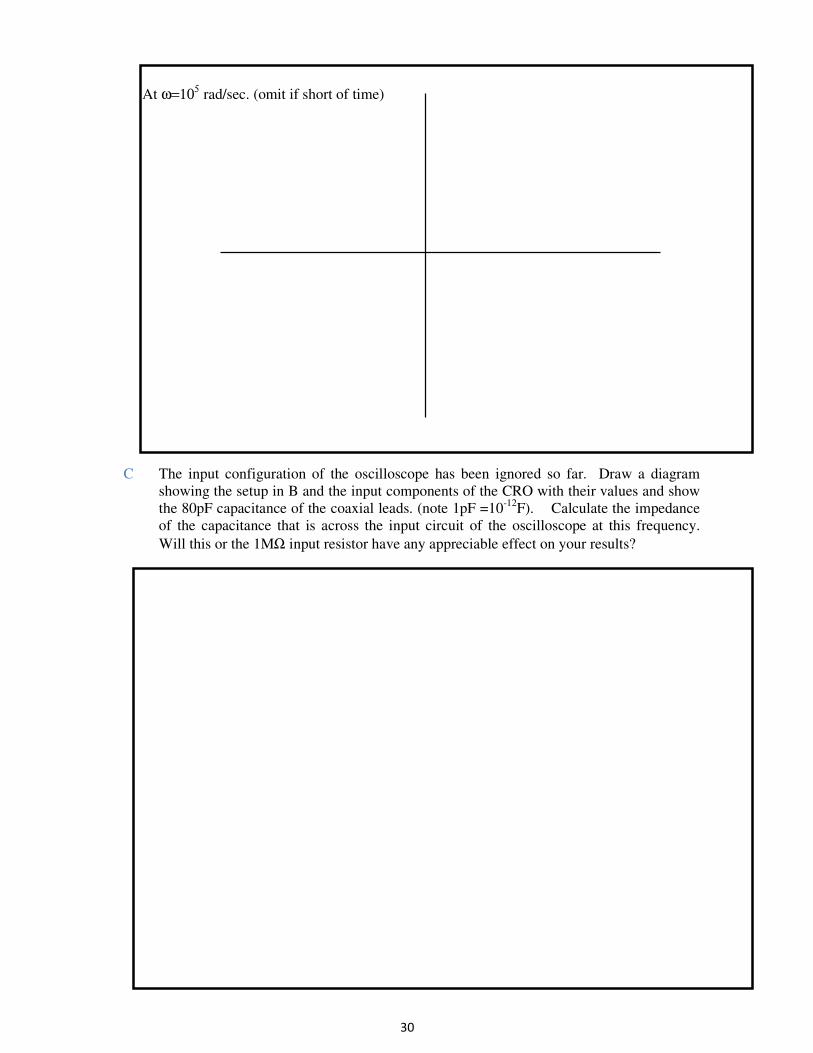
sum of the other two voltages. Redraw this diagram for ω=105 rad/sec. (By convention
the phase advances anticlockwise on the diagram)
At ω=104 rad/sec.
30
At ω=105 rad/sec. (omit if short of time)
C The input configuration of the oscilloscope has been ignored so far. Draw a diagram
showing the setup in B and the input components of the CRO with their values and show
the 80pF capacitance of the coaxial leads. (note 1pF =10-12
F). Calculate the impedance
of the capacitance that is across the input circuit of the oscilloscope at this frequency.
Will this or the 1MΩ input resistor have any appreciable effect on your results?
31
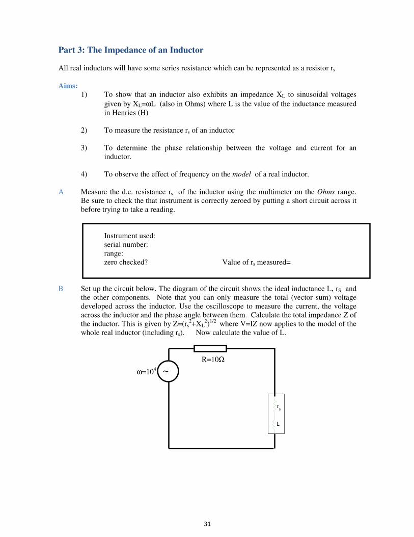
Part 3: The Impedance of an Inductor
All real inductors will have some series resistance which can be represented as a resistor rs
Aims: 1) To show that an inductor also exhibits an impedance XL to sinusoidal voltages
given by XL=ωL (also in Ohms) where L is the value of the inductance measured
in Henries (H)
2) To measure the resistance rs of an inductor
3) To determine the phase relationship between the voltage and current for an
inductor.
4) To observe the effect of frequency on the model of a real inductor.
A Measure the d.c. resistance rs of the inductor using the multimeter on the Ohms range.
Be sure to check the that instrument is correctly zeroed by putting a short circuit across it
before trying to take a reading.
Instrument used:
serial number:
range:
zero checked? Value of rs measured=
B Set up the circuit below. The diagram of the circuit shows the ideal inductance L, rS and
the other components. Note that you can only measure the total (vector sum) voltage
developed across the inductor. Use the oscilloscope to measure the current, the voltage
across the inductor and the phase angle between them. Calculate the total impedance Z of
the inductor. This is given by Z=(rs2+XL
2)1/2
where V=IZ now applies to the model of the
whole real inductor (including rs). Now calculate the value of L.
R=10Ω
ω=104 ~
r s
L

32
CALCULATIONS:
Check your values by measuring the inductor on an a.c. bridge set to represent the
inductor as two series elements. (You can also represent a real inductor or a capacitor
that is not perfect by a series or parallel combination of a resistor and an ideal
component).
bridge used: set as serial or parallel?
serial number: Measured value L=
Draw a phasor diagram for the real inductor using the measured d.c. resistance and hence
find the reactive impedance XL and then the value of the inductance from XL=ωL.
Remember to include Vs as the vector sum of the other voltages.
33
C If your supervisor feels you have enough time repeat C2 at ω=105. Notice any difference
in values and explain.
Part 4: Series Resonance L-C-R circuit
Aims:
1) To observe the resonance of a series combination of resistor, capacitor and
inductor.
2) To observe the effect of a coaxial cable lead on a circuit at high frequency.
3) To observe the relation between the supply voltage and the voltages developed
across the reactive elements at frequencies near to resonance.
You will use the inductor above and a variable capacitor of maximum value 150pF as
well as a 10Ω resistor to monitor the current. You are advised to put the capacitor as the
middle component. Remember to show the d.c. resistance of the inductor. Use should use
106
rad/sec for this part with a source voltage of about 1V peak. Draw the circuit you
think you are going to use for this a part and have it checked by your supervisor.
34
What do you think will happen to the total impedance Z of the circuit as viewed from the
source, as ω approaches zero and infinity? (consider the formulae for the impedances of
C and L from earlier)
A. Set up the circuit and adjust the variable capacitor to make the current a maximum. (Use
the oscilloscope with the screen lead on the junction of the monitoring resistor and the
capacitor.) Now the circuit is said to be resonating at ωο=106. Adjust the frequency to
about this value to see how the current responds. Note the sharpness of the response. This
is called a tuned circuit. Calculate the current at resonance and knowing the source
voltage calculate the total impedance Z of the circuit.
CALCULATIONS AND COMMENTS:
35
Under the conditions above the impedances of the inductor and the capacitor are equal in
magnitude. Given that the inductor is 10mH and the resonant frequency is
ωο=106 rad/sec, calculate the value that the variable capacitor is currently set at.
B Now connect the second input lead to the oscilloscope across the variable capacitor. The
combined capacitance of this lead and the input capacitor of the oscilloscope will cause
the circuit to have a different resonant frequency, as they are adding to the variable
capacitor. Adjust the supply frequency to obtain a new resonant frequency ω’o . Note this
frequency and hence calculate the new value for the total capacitance in the resonating
circuit. Since the value of the oscilloscope input capacitance and the variable capacitor
are known, you can calculate the capacitance of the oscilloscope lead (Because all three
components are in parallel they simply add. This would not be the case if they were
capacitors in series or if they were inductors.)

36
C You may have noticed that the voltage across the capacitor is bigger than the source
voltage. Remove the oscilloscope leads and reconnect them so that you can measure the
voltages across the variable capacitor and the inductor.
Measure these voltages in comparison with the source voltage and compare their phases.
(you may need to slightly tweak the frequency to restore resonance when you add the
oscilloscope lead across the inductor)
FINAL COMMENTS, CONCLUSIONS AND LIST OF ACHIEVED AIMS:
37
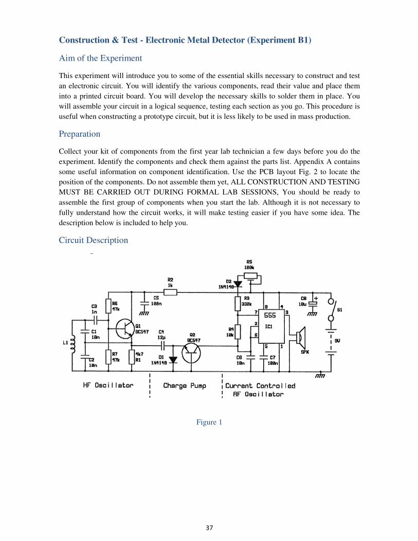
Construction & Test - Electronic Metal Detector (Experiment B1)
Aim of the Experiment
This experiment will introduce you to some of the essential skills necessary to construct and test
an electronic circuit. You will identify the various components, read their value and place them
into a printed circuit board. You will develop the necessary skills to solder them in place. You
will assemble your circuit in a logical sequence, testing each section as you go. This procedure is
useful when constructing a prototype circuit, but it is less likely to be used in mass production.
Preparation
Collect your kit of components from the first year lab technician a few days before you do the
experiment. Identify the components and check them against the parts list. Appendix A contains
some useful information on component identification. Use the PCB layout Fig. 2 to locate the
position of the components. Do not assemble them yet, ALL CONSTRUCTION AND TESTING
MUST BE CARRIED OUT DURING FORMAL LAB SESSIONS, You should be ready to
assemble the first group of components when you start the lab. Although it is not necessary to
fully understand how the circuit works, it will make testing easier if you have some idea. The
description below is included to help you.
Circuit Description
Figure 1
38
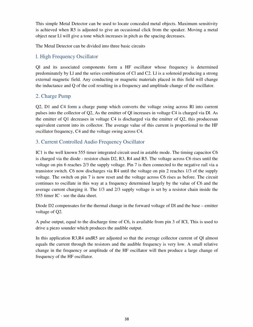
This simple Metal Detector can be used to locate concealed metal objects. Maximum sensitivity
is achieved when R5 is adjusted to give an occasional click from the speaker. Moving a metal
object near Ll will give a tone which increases in pitch as the spacing decreases.
The Metal Detector can be divided into three basic circuits
l. High Frequency Oscillator
Ql and its associated components form a HF oscillator whose frequency is determined
predominately by Ll and the series combination of Cl and C2. Ll is a solenoid producing a strong
external magnetic field. Any conducting or magnetic materials placed in this field will change
the inductance and Q of the coil resulting in a frequency and amplitude change of the oscillator.
2. Charge Pump
Q2, D1 and C4 form a charge pump which converts the voltage swing across Rl into current
pulses into the collector of Q2, As the emitter of Ql increases in voltage C4 is charged via Dl. As
the emitter of Q1 decreases in voltage C4 is discharged via the emitter of Q2, this producesan
equivalent current into its collector. The average value of this current is proportional to the HF
oscillator frequency, C4 and the voltage swing across C4.
3. Current Controlled Audio Frequency Oscillator
IC1 is the well known 555 timer integrated circuit used in astable mode. The timing capacitor C6
is charged via the diode - resistor chain D2, R3, R4 and R5. The voltage across C6 rises until the
voltage on pin 6 reaches 2/3 the supply voltage. Pin 7 is then connected to the negative rail via a
transistor switch. C6 now discharges via R4 until the voltage on pin 2 reaches 1/3 of the supply
voltage. The switch on pin 7 is now reset and the voltage across C6 rises as before. The circuit
continues to oscillate in this way at a frequency determined largely by the value of C6 and the
average current charging it. The 1/3 and 2/3 supply voltage is set by a resistor chain inside the
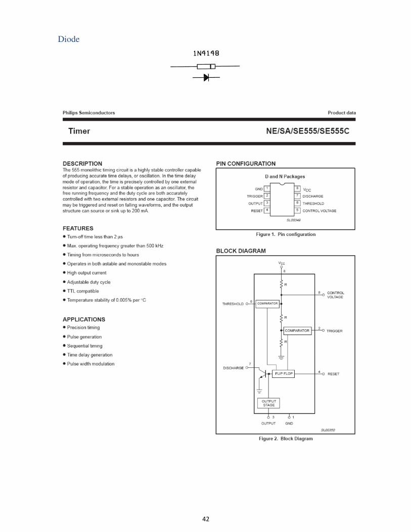
555 timer IC - see the data sheet.
Diode D2 compensates for the thermal change in the forward voltage of Dl and the base – emitter
voltage of Q2.
A pulse output, equal to the discharge time of C6, is available from pin 3 of ICI, This is used to
drive a piezo sounder which produces the audible output.
In this application R3,R4 andR5 are adjusted so that the average collector current of Ql almost
equals the current through the resistors and the audible frequency is very low. A small relative
change in the frequency or amplitude of the HF oscillator will then produce a large change of
frequency of the HF oscillator.

39
Experimental Work
The experiment is divided into three parts, each taking about two hours.
It is very important to complete each section before moving on to the next.
It is essential that the semiconductor devices and the electrolytic capacitor C8, are placed
the correct way round.
Part 1.
Hand wind 150 turns of 0.12 to 0.3mm dia. insulated copper wire on the 25mm length of ferrite.
YOU WILL NEED TO STRIP THE PLASTIC COATING FROM THE ENDS OF THE
COPPER WIRE USING SANDPAPER BEFORE YOU SOLDER IT TO THE CIRCUIT –
Check the resistance of the coil this with a mulimeter to make sure all the coating is removed at
the contacts. Assemble all the components for the HF oscillator and charge pump. Temporarily
solder two leads to your PCB to provide the 9 Volt power supply. Set a bench power supply to
9V and low current limit. Apply this supply to your board and check the supply current is not
excessive ( < 5mA). Using an oscilloscope check the oscillator output across Rl is 100-330 kHz
and greater than 5V peak to peak. If no output is detected switch off the power and check the
location of all he components. Also check for short circuits due to excess solder. Continue fault
finding until the oscillator is working correctly.
Part 2.
Temporarily solder a wire to the PCB to make connection to the collector of Q2. Connect a
digital multimeter between this wire and the 9V positive supply rail.
Adjust the current to 7.0 µA by changing the number of turns on Ll. If necessary a larger change
may be made by changing the value of C4. Measure the change in current as a sample steel screw
is moved close to Ll. Remove the wire connected to the collector of Q2.
Part 3.
Assemble the rest of the components on the printed circuit board. Reconnect the power supply
and again check the current consumption is not excessive ( < 10 mA ). Adjust R5 to give an
occasional click from the speaker. If no audible output is heard switch off the power and check
the location of the added components. Check the operation of the circuit at reduced voltage; it
should continue to work down to at least 7V. If the null point cannot be set over this range it may
be necessary to adjust the number of turns on the coil L1.
Finally, check the operation of the metal detector using the sample screw.
40
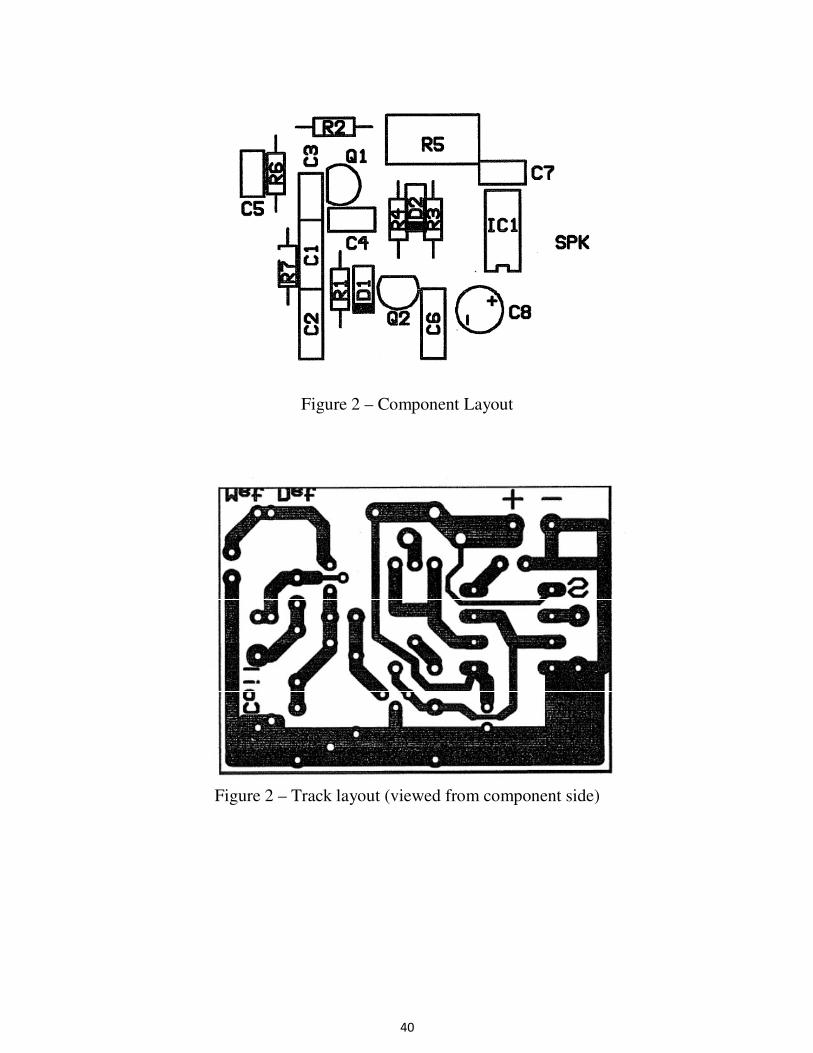
Figure 2 – Component Layout
Figure 2 – Track layout (viewed from component side)
41
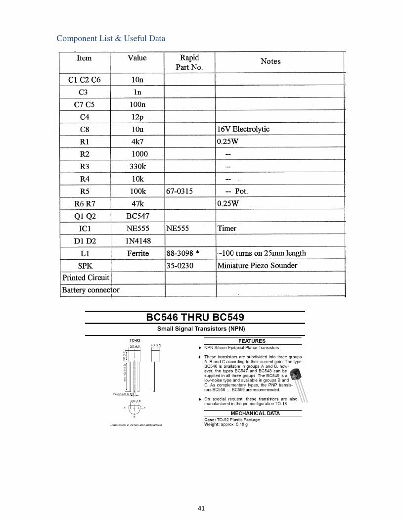
Component List & Useful Data
42
Diode
43
Microphone pre-amplifier construction
(Experiment B1 for media engineers)
Aim of the experiment
This experiment will introduce you to some of the essential skills necessary to construct and test
an electronic circuit. You will identify the various components, read their value and place them
into a printed circuit board. You will develop the necessary skills to solder them in place.
You will assemble your circuit in a logical sequence, testing each section as you go. This
procedure is useful when constructing a prototype circuit, it is less likely to be used in mass
production.
Preparation
You may collect your kit of components from the first-year lab technician a few days before you
do the experiment. Identify the components and check them against the parts list. The Appendix
contains some useful information on component identification. Use the PCB layout in Figure 2 to
locate the position of the components. Do not assemble them yet, as all construction and testing
must be carried out during formal lab sessions. You should be ready to assemble the first group
of components when you start the lab.
Although it is not necessary to understand fully how the circuit works, it will make testing easier
if you have some idea. The description below is included to help you.
Circuit description
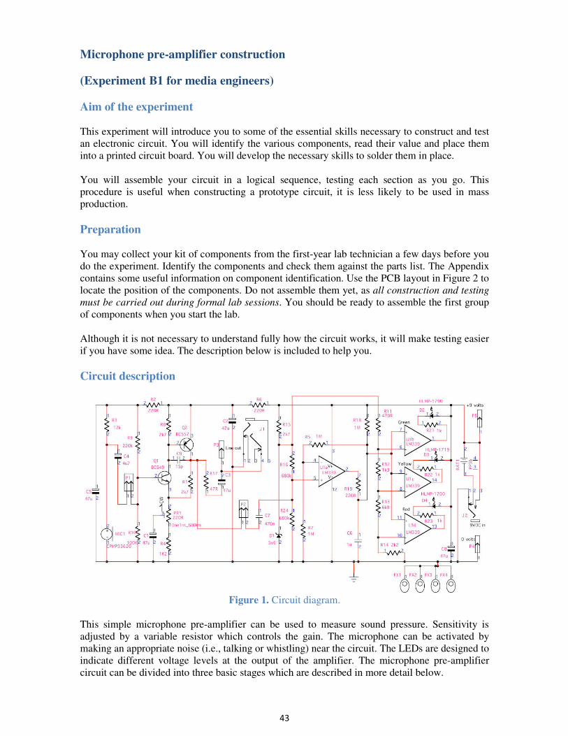
Figure 1. Circuit diagram.
This simple microphone pre-amplifier can be used to measure sound pressure. Sensitivity is
adjusted by a variable resistor which controls the gain. The microphone can be activated by
making an appropriate noise (i.e., talking or whistling) near the circuit. The LEDs are designed to
indicate different voltage levels at the output of the amplifier. The microphone pre-amplifier
circuit can be divided into three basic stages which are described in more detail below.

44
1. Microphone coupling
The resistors and capacitors surrounding the microphone in the first stage are designed to provide
the microphone capsule with a DC power supply. The DC voltage is then isolated from the
amplifier by capacitor C4, which at the same time admits the AC signal generated across the
microphone terminals. Together these components constitute a simple kind of band-pass filter
whose cut-on and cut-off frequencies are determined by the resistor and capcitor values.
2. Audio pre-amplifier
The second stage amplifies the small AC signal from the microphone up to a line level, where it
could be interfaced to other audio devices. The network of resistors is designed to set the correct
DC operating point for the transistors, as well as determining their AC gain. Thus, the gain of
this amplification stage can be adjusted by the potentiometer PR1 whose central connection acts
effectively as a ground for AC signals by the action of capacitor C1.
3. Voltage-level comparators
The third stage of the circuit uses the audio signal to determine the voltage level across a
capacitor (C6). The operation of three coloured LEDs is switched by comparing this voltage to
three different reference voltages.
With zero AC signal coming from the amplifier, the open-collector output of comparator U1a is
off and C6 is charged up by current through large resistor R18. The voltage depends on that
across D1, the potential divider R16 and R24, and the gain circuit R5 and R7 (and R19). When
an AC signal turns the comparator on, it then discharges the capacitor and reduces the voltage
across it.
The three further comparators controlling the LEDs (U1b, U1c and U1d) are switched on and off
depending on whether the voltage across C6 dips below their corresponding reference levels.
These reference voltages are determined by the voltage across the Zener diode D1 and the
potential divider resistors R11, R12, R13 and R14.
Experimental work
The experiment is divided into three parts, corresponding to each of the three stages just
described. It is necessary to complete each part before moving onto the next. You should record
any tests, measurents or modifications made to your circuits during construction in your log
book. See the circuit board layout diagram (figure 2) to locate and place components.
It is essential that the microphone, the semiconductor devices (chip, transistors and diodes)
and the electrolytic capacitors (C1, C2, C3, C4, C5 and C8) are placed with the correct
polarity.
Part 1. Microphone coupling
Solder the components for the first stage onto the printed circuit board that you have been given,
then attach two leads to your PCB to provide the 9 Volt power supply. Set a bench power supply
to 9V and low current limit. Apply this supply to your board and check the supply is not
excessive (i.e., <5 mA).
Using an oscilloscope, check the microphone output at P1 (across C4 and MIC1). You should
see an alternating signal that responds to any sounds you make. Record the typical voltage level
for speech while talking normally at a distance of about 20 cm from the capsule. If no output is

45
detected, switch off the power supply and check the location and polarity of all the components.
Also check for short circuits due to excess solder. Continue fault finding until the microphone is
working correctly.
Part 2. Audio pre-amplifier
Assemble and solder the components for the second stage of the circuit. Test the output of
amplifier at P2 by observing the signal on an oscilloscope. Make sure that the shape of the signal
is similar to that observed at the lower level from the output of the microphone. The alternating
signal should have both positive and negative parts (viewed on AC coupling) and not appear
clipped or distorted.
Record the typical voltage level for speech as before and make an estimate of the gain. Vary the
value of the resistance PR1 and observe how it affects the gain. Finally, adjust the gain to be
approximately half that given by the maximum setting.
Part 3. Voltage-level comparators
Assemble the components for the third stage of the circuit. Be careful not to overheat the legs of
the chip and ensure the correct orientation of all the diodes. Once you have reconnected the
power supply, you should observe that the LEDs respond to sounds of different intensities.
Attach an oscilloscope probe across C6 in the circuit (you may need to hook onto the leg of a
connected resistor) and observe the DC voltage. When quiet, the voltage level should float at a
constant value. Record this voltage. How does it compare to the voltage across D1? Also observe
how the voltage across the capacitor discharges through the comparator U1a as the sound level
increases.
Evaluate your circuit's performance by probing it with some tests, noting any results in your log
book, together with a summary of what you have achieved and learnt from this experiment. You
have now completed the construction experiment: you can try to listen to the amplifier output on
some headphones and you can adjust the gain as you please!
46
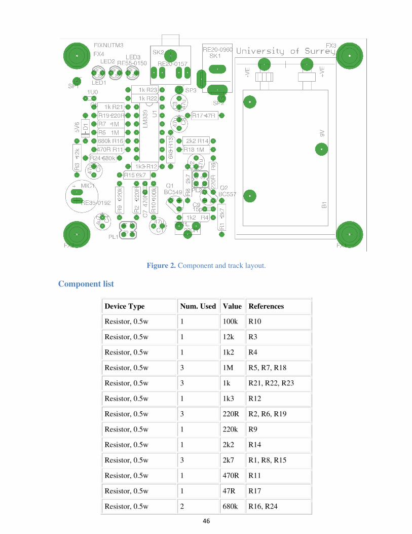
Figure 2. Component and track layout.
Component list
Device Type Num. Used Value References
Resistor, 0.5w 1 100k R10
Resistor, 0.5w 1 12k R3
Resistor, 0.5w 1 1k2 R4
Resistor, 0.5w 3 1M R5, R7, R18
Resistor, 0.5w 3 1k R21, R22, R23
Resistor, 0.5w 1 1k3 R12
Resistor, 0.5w 3 220R R2, R6, R19
Resistor, 0.5w 1 220k R9
Resistor, 0.5w 1 2k2 R14
Resistor, 0.5w 3 2k7 R1, R8, R15
Resistor, 0.5w 1 470R R11
Resistor, 0.5w 1 47R R17
Resistor, 0.5w 2 680k R16, R24
47
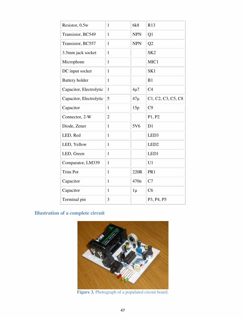
Resistor, 0.5w 1 6k8 R13
Transistor, BC549 1 NPN Q1
Transistor, BC557 1 NPN Q2
3.5mm jack socket 1 SK2
Microphone 1 MIC1
DC input socket 1 SK1
Battery holder 1 B1
Capacitor, Electrolytic 1 4µ7 C4
Capacitor, Electrolytic 5 47µ C1, C2, C3, C5, C8
Capacitor 1 15p C9
Connector, 2-W 2 P1, P2
Diode, Zener 1 5V6 D1
LED, Red 1 LED3
LED, Yellow 1 LED2
LED, Green 1 LED1
Comparator, LM339 1 U1
Trim Pot 1 220R PR1
Capacitor 1 470n C7
Capacitor 1 1µ C6
Terminal pin 3 P3, P4, P5
Illustration of a complete circuit
Figure 3. Photograph of a populated circuit board.
48
Combinational Logic (Experiment B2).
Aims of the Experiment.
This experiment illustrates the elementary ideas and applications of Boolean algebra and
combinational logic.
1. Explore the theory outlined in this experiment,
2. Apply the theory to design logic circuits.
3. Implement logic circuits to confirm operation.
Introduction.
Gates and Logical Operators:
In electronic logic circuits two states are defined corresponding to two distinct voltage levels.
These voltage levels represent the binary numbers “1” and “0” which correspond to the “True”
and “False” of logic. In typical circuits 5-volts would represent a logic 1 and 0-volts (typically a
few milli-volts but close to 0) would represent a logic 0. However this is sometimes reversed
depending upon the application of the circuit, or the voltage levels might change dramatically
(Consider CMOS logic as an example).
Three logic operations (implemented by using logic gates) are considered in this experiment.
Each one will be denoted by a circuit symbol and a truth table which shows all possible input
combinations and the corresponding output from the operation. Note that all voltage levels in the
logic circuits are referenced to a common reference voltage (in the experiment this is earth) and
this is therefore omitted from the symbolic representation. The symbol convention used in this
experiment conforms to the IEEE Std. 91a-1991 and the distinctive symbol convention.
49
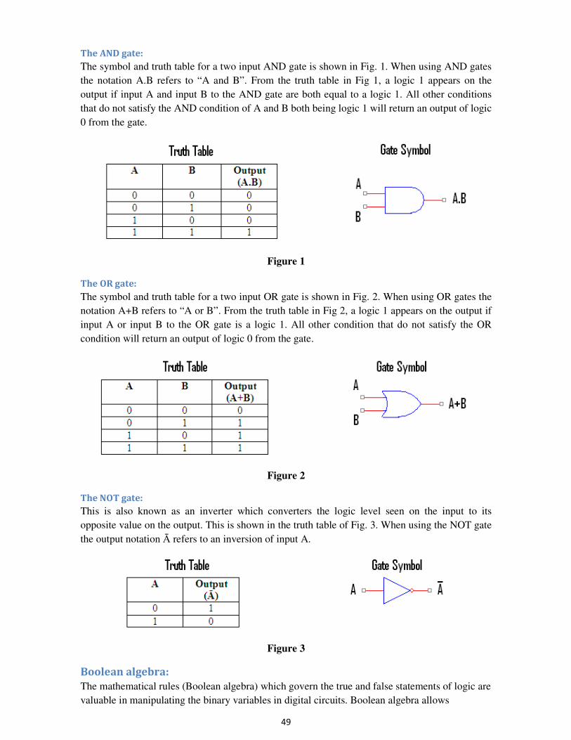
The AND gate:
The symbol and truth table for a two input AND gate is shown in Fig. 1. When using AND gates
the notation A.B refers to “A and B”. From the truth table in Fig 1, a logic 1 appears on the
output if input A and input B to the AND gate are both equal to a logic 1. All other conditions
that do not satisfy the AND condition of A and B both being logic 1 will return an output of logic
0 from the gate.
Figure 1
The OR gate:
The symbol and truth table for a two input OR gate is shown in Fig. 2. When using OR gates the
notation A+B refers to “A or B”. From the truth table in Fig 2, a logic 1 appears on the output if
input A or input B to the OR gate is a logic 1. All other condition that do not satisfy the OR
condition will return an output of logic 0 from the gate.
Figure 2
The NOT gate:
This is also known as an inverter which converters the logic level seen on the input to its
opposite value on the output. This is shown in the truth table of Fig. 3. When using the NOT gate
the output notation Ā refers to an inversion of input A.
Figure 3
Boolean algebra:
The mathematical rules (Boolean algebra) which govern the true and false statements of logic are
valuable in manipulating the binary variables in digital circuits. Boolean algebra allows
50
complicated logic statements to be simplified so that the minimum numbers of logic gates are
used for a given requirement. They also allow certain gates to be used to fulfil the function of
other gates (such as using only NAND gates in a circuit which reduces cost). Consider the set of
Boolean theorems shown in Fig. 4 for a single variable.
OR AND NOT
A + 0 = A A.0 = 0 Ā = A
A + 1 = 1 A.1 = A
A + A = A A.A = A
A + Ā = 1 A. Ā = 0
Figure 4
Boolean theorems with more than one variable are shown in Fig 5.
Commutation
Rules
Association Rules Absorption
Rules
Distribution Rules
A+B = B+A A+(B+C) = (A+B)+C A+(A.B) = A A.(B+C) = (A.B)+(A.C)
A.B = B.A A.(B.C) = (A.B).C A.(A+B) = A A+(B.C) = (A+B).(A+C)
Figure 5
The truth table of figure 6 illustrates the first absorption rule. Comparing the first and last
columns of Fig 6 the expression A+(A.B) = A is proved.
Inputs Output
A B A.B A+(A.B)
0 0 0 0
0 1 0 0
1 0 0 1
1 1 1 1
Figure 6
In general however the last column may not be simply related to the input A. By ignoring for the
time being the relationship between A and the output, the Boolean expression to represent the
output is better generated by comparing the output column with the input columns. By
comparing the instances when the output is equal to a logic 1 with the inputs we can obtain the
expression:
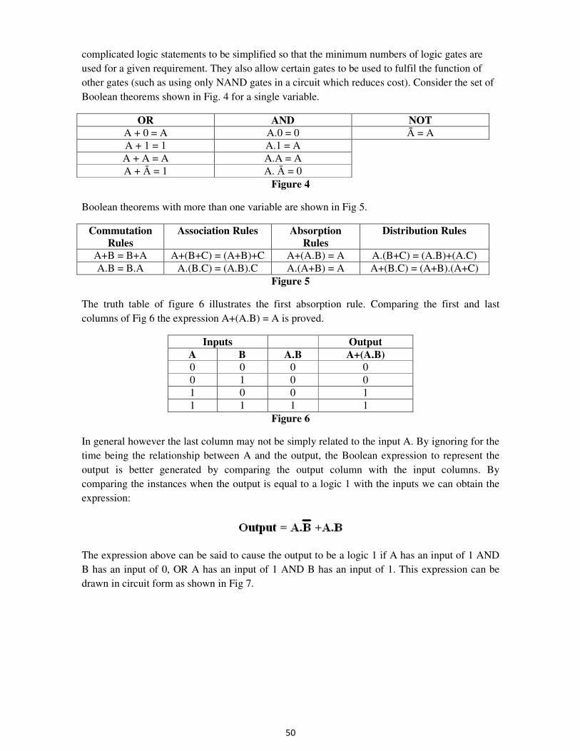
The expression above can be said to cause the output to be a logic 1 if A has an input of 1 AND
B has an input of 0, OR A has an input of 1 AND B has an input of 1. This expression can be
drawn in circuit form as shown in Fig 7.
51
Figure 7
Fig 7 does use a lot of different gates which is expensive in cost and space. It can be simplified
as follows:
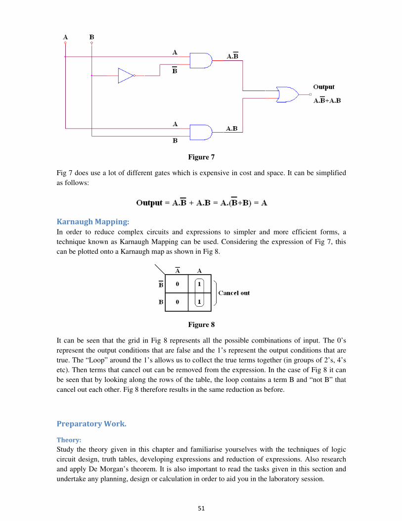
Karnaugh Mapping:
In order to reduce complex circuits and expressions to simpler and more efficient forms, a
technique known as Karnaugh Mapping can be used. Considering the expression of Fig 7, this
can be plotted onto a Karnaugh map as shown in Fig 8.
Figure 8
It can be seen that the grid in Fig 8 represents all the possible combinations of input. The 0’s
represent the output conditions that are false and the 1’s represent the output conditions that are
true. The “Loop” around the 1’s allows us to collect the true terms together (in groups of 2’s, 4’s
etc). Then terms that cancel out can be removed from the expression. In the case of Fig 8 it can
be seen that by looking along the rows of the table, the loop contains a term B and “not B” that
cancel out each other. Fig 8 therefore results in the same reduction as before.
Preparatory Work.
Theory:
Study the theory given in this chapter and familiarise yourselves with the techniques of logic
circuit design, truth tables, developing expressions and reduction of expressions. Also research
and apply De Morgan’s theorem. It is also important to read the tasks given in this section and
undertake any planning, design or calculation in order to aid you in the laboratory session.
52
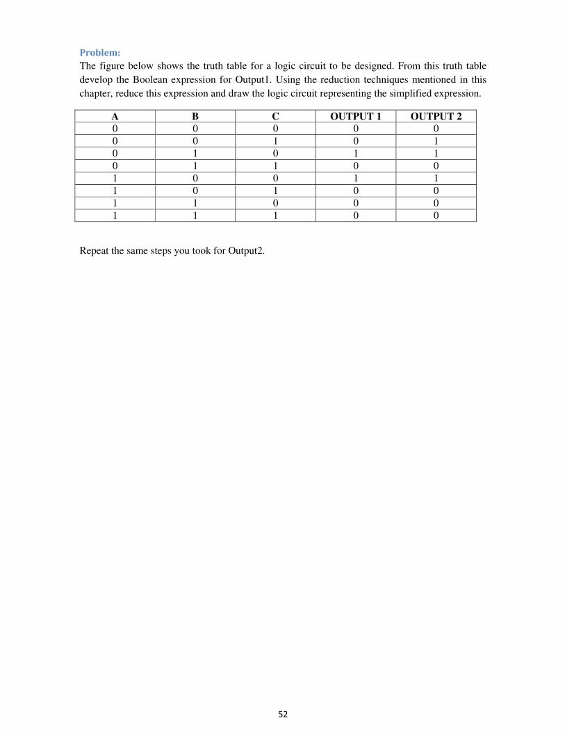
Problem:
The figure below shows the truth table for a logic circuit to be designed. From this truth table
develop the Boolean expression for Output1. Using the reduction techniques mentioned in this
chapter, reduce this expression and draw the logic circuit representing the simplified expression.
A B C OUTPUT 1 OUTPUT 2
0 0 0 0 0
0 0 1 0 1
0 1 0 1 1
0 1 1 0 0
1 0 0 1 1
1 0 1 0 0
1 1 0 0 0
1 1 1 0 0
Repeat the same steps you took for Output2.
53
Experimental Work.
Familiarise yourself with the logic boxes that will be used throughout the experimental part of
this laboratory. It is worth noting that any unconnected inputs to the gates may cause the gates to
behave in an unpredictable way. Un-used inputs to logic gates are generally tide to a high logic
input or low logic input in order to ensure correct circuit operation.
The experimental work in this laboratory is divided into a number of tasks.
Task One:
Verify the following theorems using logic circuits:
Task Two:
Apply and verify De Morgan’s Theorems:
Task Three:
In this task we will develop a circuit to illuminate a lamp when two out of three inputs are driven
high (logic 1). Construct a truth table that shows the output being driven high when only two out
of three of the inputs are high. From the truth table write down the appropriate expression and
draw the logic circuit. Finally test your design against the specification.
Task Four:
Design and test a logic network with three inputs A, B and C that will only light a lamp if:
1. Input A and C are logic 1 and B is at a logic 0, or
2. Input A and B are at logic 1 and C is at logic 0, or
3. A is at logic 1 and B and C are at logic 0.
Task Five:
A common arithmetic operation used in digital computing is the addition of two binary numbers.
The circuits presented in this task enable this operation to be performed.
The Half Adder:
The truth table for a binary half adder is shown in Fig 9. The inputs A and B are the binary digits
to be added. Construct the logic circuit to test this truth table so that a lamp represents the SUM
and CARRY output.

54
A B SUM CARRY
0 0 0 0
0 1 1 0
1 0 1 0
1 1 0 1
Figure 9
The SUM output uses a logic operation known as an exclusive-OR and has the symbol . It can
be shown that:
Experimentally compare the two logic circuits based on the expressions below.
The Full Adder:
Write the truth table for a binary full adder that has two inputs A and B and a third input that
represents the carry terms to be added to A and B. From this truth table derive an expression for
the SUM output. Through experimentation show that the carry term is given by:
Further Work:
If time permits and the previous tasks have been completed then consider completing the
following further tasks.
Further Task One:
A frequent operation that is undertaken in digital systems is the comparison of binary numbers to
determine if one is greater than or equal to the other. Design a logic circuit with two inputs A and
B, and three outputs that will illuminate lamp one if the A > B, lamp two if A = B and the third
lamp if A < B.
Further Task Two:
Design a voting system for three people such that lamp one is illuminated if a majority vote “In
Favour” is obtained, and lamp two is illuminated if a majority “Against” is obtained.
Further Task Three:
Develop a voting system that now considers four voters, but will not allow lamps to be
illuminated under tie conditions.
Further Task Four:
Design a half subtractor and verify its operation through experimentation.
Further Task Five:
Develop a full subtractor and verify its operation through experimentation.
55
Measurement Circuits (Experiment B3).
Aims of the Experiment.
The measurement of voltage, current and resistance is an essential part of any electronic system.
This experiment illustrates the elementary principles and techniques for measuring these circuit
parameters.
1. Explore the basic methods of measuring Voltage, Current and Resistance,
2. Design simple measuring circuits,
3. Construct and test simple measuring circuits,
4. Design and test improved measuring circuits using Op-Amps.
Introduction.
The moving coil milli-ammeter:
One of basic methods of measurement is the use of the moving coil meter. These coils are
characterized by two very important characteristics. The first is the full-scale current. This
characterizes the amount of current needed to move the needle of the coil to the full-scale
deflection position. The second important characteristic is the resistance of the coil. These two
characteristics are all that is needed in order to design circuits to measure voltage, current and
resistance using a moving coil.
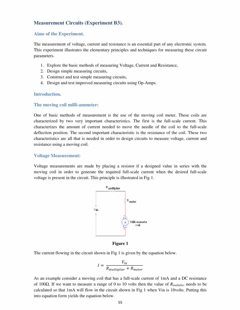
Voltage Measurement:
Voltage measurements are made by placing a resistor if a designed value in series with the
moving coil in order to generate the required full-scale current when the desired full-scale
voltage is present in the circuit. This principle is illustrated in Fig 1.
Figure 1
The current flowing in the circuit shown in Fig 1 is given by the equation below.
= +
As an example consider a moving coil that has a full-scale current of 1mA and a DC resistance
of 100Ω. If we want to measure a range of 0 to 10 volts then the value of Rmultiplier needs to be
calculated so that 1mA will flow in the circuit shown in Fig 1 when Vin is 10volts. Putting this
into equation form yields the equation below.

56
=
−
= 101 − 100 = 9900
From this equation it can be seen that the total resistance in the circuit will be Rmultiplier+Rmeter
which is 10000Ω. By definition the sensitivity of a voltmeter constructed according to Fig 1 is
the ratio of total resistance to full-scale voltage, and is equal to the reciprocal of the full-scale
current as shown below.
!"!#!"$ = 1
= %ℎ' ()"
This shows that a circuit with a 1mA meter will always have a sensitivity of 1000Ω/V.
57
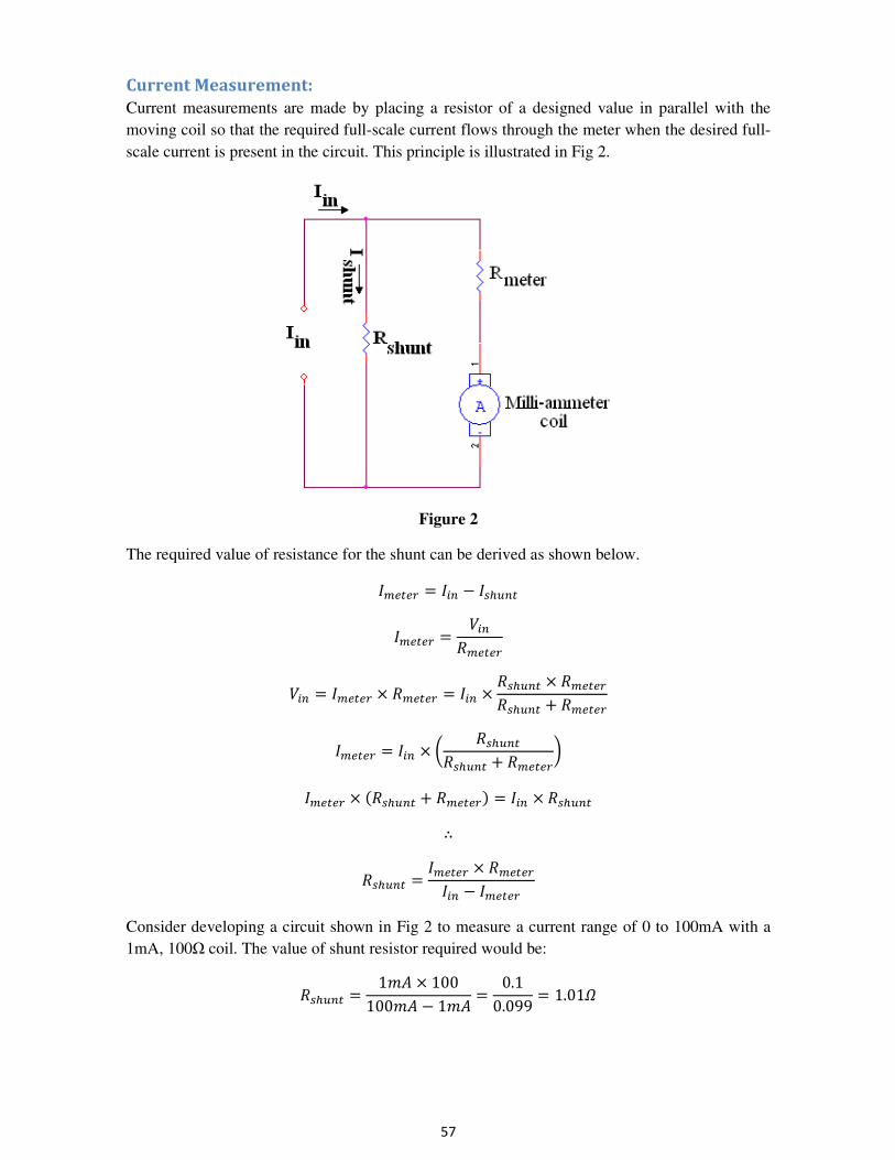
Current Measurement:
Current measurements are made by placing a resistor of a designed value in parallel with the
moving coil so that the required full-scale current flows through the meter when the desired full-
scale current is present in the circuit. This principle is illustrated in Fig 2.
Figure 2
The required value of resistance for the shunt can be derived as shown below.
= − *+
=
= × = × *+ × *+ +
= × *+*+ +
× -*+ + . = × *+
∴
*+ = × −
Consider developing a circuit shown in Fig 2 to measure a current range of 0 to 100mA with a
1mA, 100Ω coil. The value of shunt resistor required would be:
*+ = 1'0 × 100100'0 − 1'0 = 0.1
0.099 = 1.01
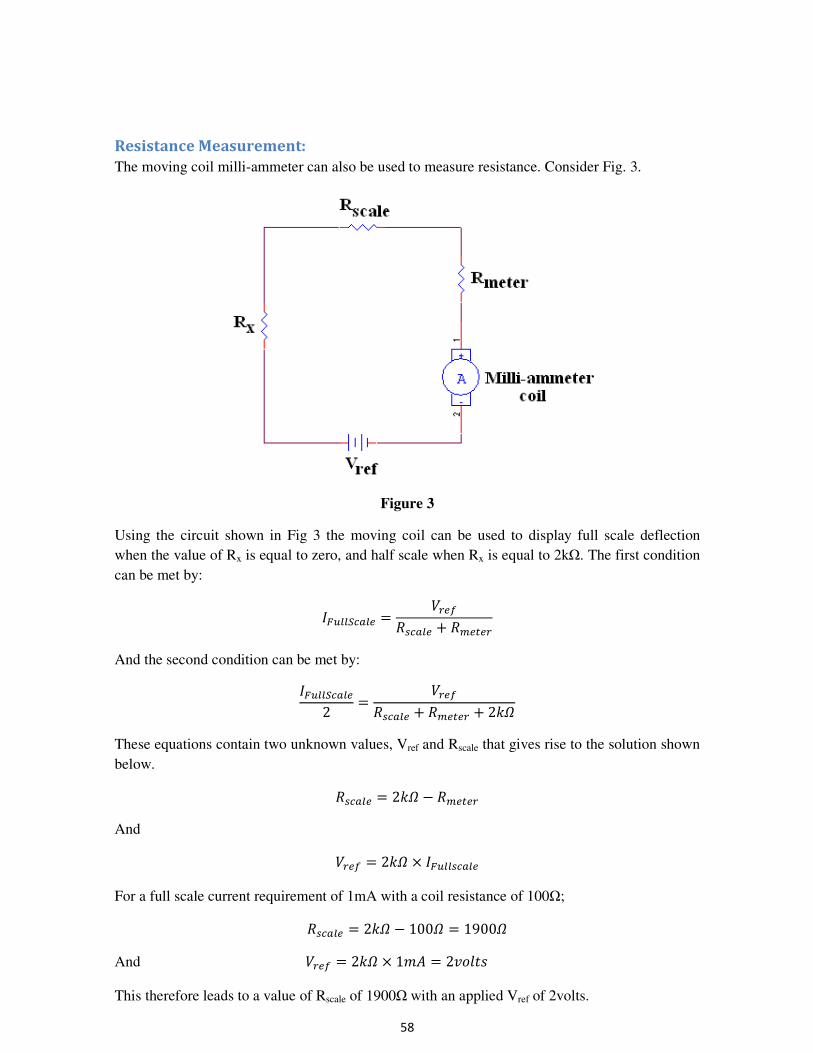
58
Resistance Measurement:
The moving coil milli-ammeter can also be used to measure resistance. Consider Fig. 3.
Figure 3
Using the circuit shown in Fig 3 the moving coil can be used to display full scale deflection
when the value of Rx is equal to zero, and half scale when Rx is equal to 2kΩ. The first condition
can be met by:
= 2* +
And the second condition can be met by:
2 = 2
* + + 24
These equations contain two unknown values, Vref and Rscale that gives rise to the solution shown
below.
* = 24 −
And
2 = 24 × *
For a full scale current requirement of 1mA with a coil resistance of 100Ω;
* = 24 − 100 = 1900
And 2 = 24 × 1'0 = 2#()"
This therefore leads to a value of Rscale of 1900Ω with an applied Vref of 2volts.
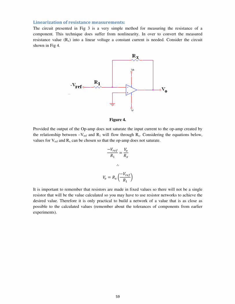
59
Linearization of resistance measurements:
The circuit presented in Fig 3 is a very simple method for measuring the resistance of a
component. This technique does suffer from nonlinearity. In over to convert the measured
resistance value (Rx) into a linear voltage a constant current is needed. Consider the circuit
shown in Fig 4.
Figure 4.
Provided the output of the Op-amp does not saturate the input current to the op-amp created by
the relationship between –Vref and R1 will flow through Rx. Considering the equations below,
values for Vref and Rx can be chosen so that the op-amp does not saturate.
− 25
= 67
∴
6 = 7 − 25
It is important to remember that resistors are made in fixed values so there will not be a single
resistor that will be the value calculated so you may have to use resistor networks to achieve the
desired value. Therefore it is only practical to build a network of a value that is as close as
possible to the calculated values (remember about the tolerances of components from earlier
experiments).
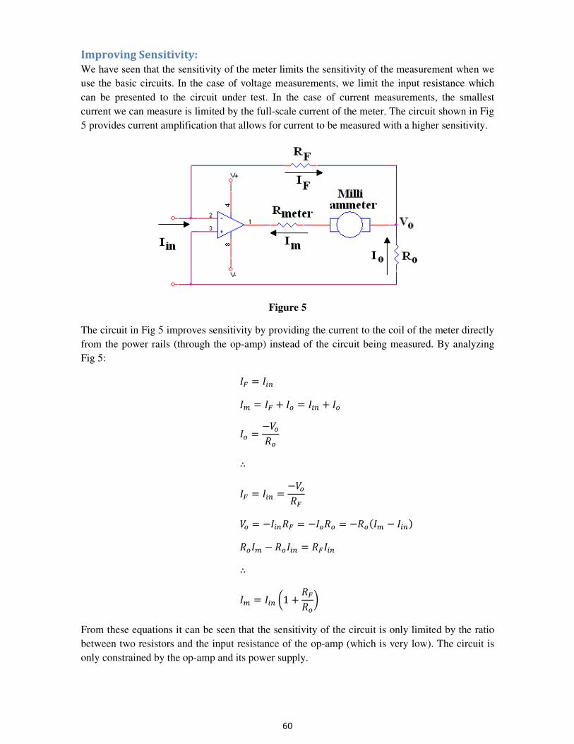
60
Improving Sensitivity:
We have seen that the sensitivity of the meter limits the sensitivity of the measurement when we
use the basic circuits. In the case of voltage measurements, we limit the input resistance which
can be presented to the circuit under test. In the case of current measurements, the smallest
current we can measure is limited by the full-scale current of the meter. The circuit shown in Fig
5 provides current amplification that allows for current to be measured with a higher sensitivity.
Figure 5
The circuit in Fig 5 improves sensitivity by providing the current to the coil of the meter directly
from the power rails (through the op-amp) instead of the circuit being measured. By analyzing
Fig 5:
=
= + 6 = + 6
6 = −66
∴
= = −6
6 = − = −66 = −6- − .
6 − 6 =
∴
= 1 + 6
From these equations it can be seen that the sensitivity of the circuit is only limited by the ratio
between two resistors and the input resistance of the op-amp (which is very low). The circuit is
only constrained by the op-amp and its power supply.
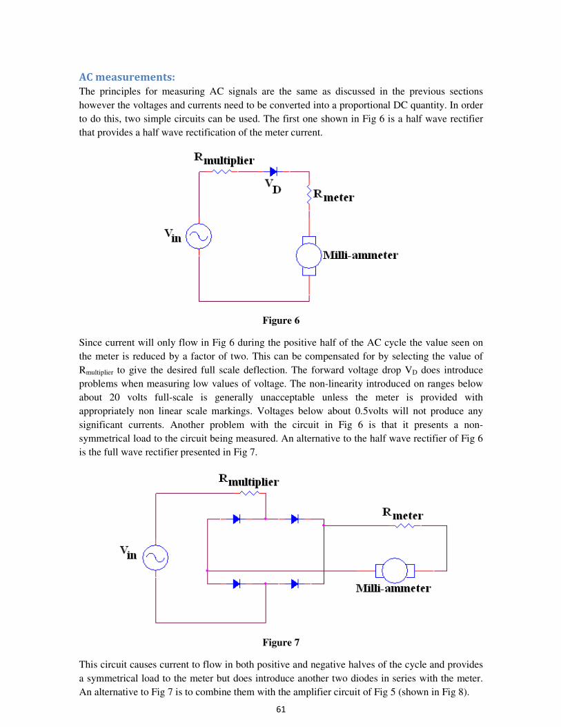
61
AC measurements:
The principles for measuring AC signals are the same as discussed in the previous sections
however the voltages and currents need to be converted into a proportional DC quantity. In order
to do this, two simple circuits can be used. The first one shown in Fig 6 is a half wave rectifier
that provides a half wave rectification of the meter current.
Figure 6
Since current will only flow in Fig 6 during the positive half of the AC cycle the value seen on
the meter is reduced by a factor of two. This can be compensated for by selecting the value of
Rmultiplier to give the desired full scale deflection. The forward voltage drop VD does introduce
problems when measuring low values of voltage. The non-linearity introduced on ranges below
about 20 volts full-scale is generally unacceptable unless the meter is provided with
appropriately non linear scale markings. Voltages below about 0.5volts will not produce any
significant currents. Another problem with the circuit in Fig 6 is that it presents a non-
symmetrical load to the circuit being measured. An alternative to the half wave rectifier of Fig 6
is the full wave rectifier presented in Fig 7.
Figure 7
This circuit causes current to flow in both positive and negative halves of the cycle and provides
a symmetrical load to the meter but does introduce another two diodes in series with the meter.
An alternative to Fig 7 is to combine them with the amplifier circuit of Fig 5 (shown in Fig 8).
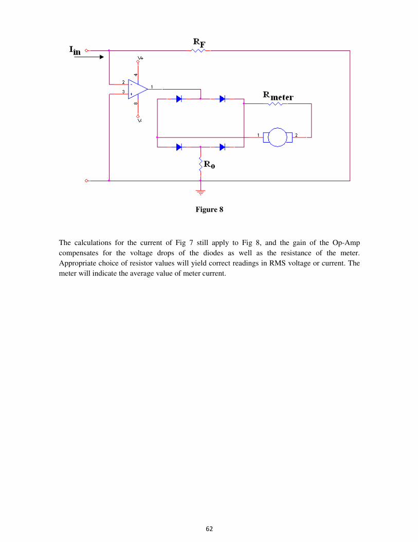
62
Figure 8
The calculations for the current of Fig 7 still apply to Fig 8, and the gain of the Op-Amp
compensates for the voltage drops of the diodes as well as the resistance of the meter.
Appropriate choice of resistor values will yield correct readings in RMS voltage or current. The
meter will indicate the average value of meter current.

63
Preparatory Work.
The coil-meter used in this lab has an internal resistance of 60Ω and reads 0 to 1mA full-scale.
As part of your preparation circuits should be drawn and the value of components for each task
should be calculated.
Experimental work:
The experiment in this lab consists of a number of tasks that will demonstrate the principles of
measuring circuits described in this section.
Task One:
Build a voltmeter that reads 0 to 10volts DC full-scale and verify its accuracy using a DVM as
reference.
Task Two:
Modify the circuit developed in task 1 to read 0 to 10volts AC full-scale and verify its accuracy
and the linearity.
Task Three:
Build a milli-ammeter to read 0 to 100mA full-scale and check its accuracy and linearity. It is
very important to ensure that good connections are made and that the value of shunt
resistor calculated is correct as it can damage the meter. If in doubt get the circuit and
values checked.
Task Four:
Build an ohmmeter to read a 20KΩ value in the centre of the meters scale. Check the accuracy of
your meter. What are the lowest and highest values of resistance that can accurately be measured
using your circuit?
Task Five:
Using the circuit from Fig 4, build an ohmmeter that will read 1MegΩ full-scale and check its
accuracy. What are the lowest and highest values of resistance that can accurately be measured
using this circuit?
Task Six:
Build the circuit shown in Fig 5 using suitable calculated values that will form a voltmeter with a
sensitivity of 10,000ohms/volt. Check the sensitivity, accuracy and linearity of this circuit.
Task Seven:
Modify the circuit for task six to make an AC measurement, and again check the accuracy and
linearity.
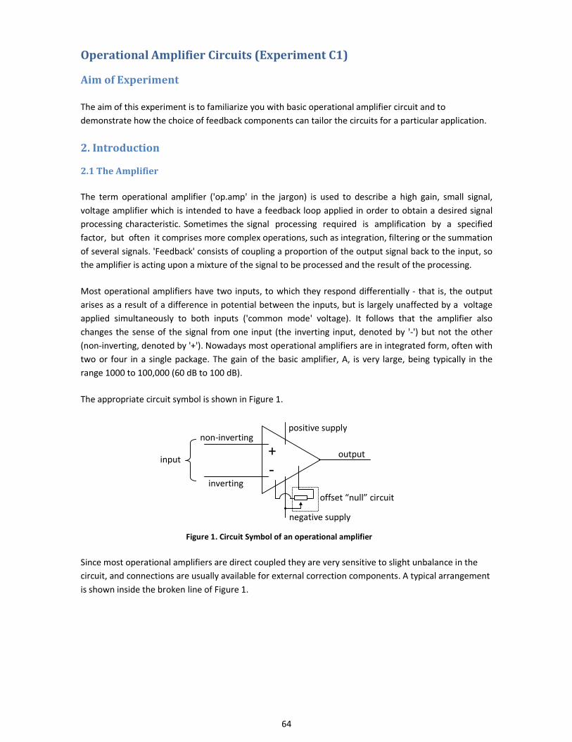
64
Operational Amplifier Circuits (Experiment C1)
Aim of Experiment
The aim of this experiment is to familiarize you with basic operational amplifier circuit and to
demonstrate how the choice of feedback components can tailor the circuits for a particular application.
2. Introduction
2.1 The Amplifier
The term operational amplifier ('op.amp' in the jargon) is used to describe a high gain, small signal,
voltage amplifier which is intended to have a feedback loop applied in order to obtain a desired signal
processing characteristic. Sometimes the signal processing required is amplification by a specified
factor, but often it comprises more complex operations, such as integration, filtering or the summation
of several signals. 'Feedback' consists of coupling a proportion of the output signal back to the input, so
the amplifier is acting upon a mixture of the signal to be processed and the result of the processing.
Most operational amplifiers have two inputs, to which they respond differentially - that is, the output
arises as a result of a difference in potential between the inputs, but is largely unaffected by a voltage
applied simultaneously to both inputs ('common mode' voltage). It follows that the amplifier also
changes the sense of the signal from one input (the inverting input, denoted by '-') but not the other
(non-inverting, denoted by '+'). Nowadays most operational amplifiers are in integrated form, often with
two or four in a single package. The gain of the basic amplifier, A, is very large, being typically in the
range 1000 to 100,000 (60 dB to 100 dB).
The appropriate circuit symbol is shown in Figure 1.
Since most operational amplifiers are direct coupled they are very sensitive to slight unbalance in the
circuit, and connections are usually available for external correction components. A typical arrangement
is shown inside the broken line of Figure 1.
output input
non-inverting positive supply
+
- inverting
negative supply
offset “null” circuit
Figure 1. Circuit Symbol of an operational amplifier
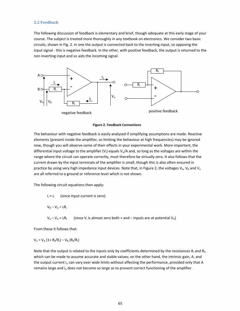
65
2.2 Feedback
The following discussion of feedback is elementary and brief, though adequate at this early stage of your
course. The subject is treated more thoroughly in any textbook on electronics. We consider two basic
circuits, shown in Fig. 2. In one the output is connected back to the inverting input, so opposing the
input signal - this is negative feedback. In the other, with positive feedback, the output is returned to the
non inverting input and so aids the incoming signal.
The behaviour with negative feedback is easily analysed if simplifying assumptions are made. Reactive
elements (present inside the amplifier, so limiting the behaviour at high frequencies) may be ignored
now, though you will observe some of their effects in your experimental work. More important, the
differential input voltage to the amplifier (VI) equals Vo/A and, so long as the voltages are within the
range where the circuit can operate correctly, must therefore be virtually zero. It also follows that the
current drawn by the input terminals of the amplifier is small, though this is also often ensured in
practice by using very high impedance input devices. Note that, in Figure 2, the voltages VA, VB and Vo
are all referred to a ground or reference level which is not shown.
The following circuit equations then apply:
ii = if (since input current is zero)
VB – VA = iiRi
Vo – VA = ifRf (since Vi is almost zero both + and – inputs are at potential VA)
From these it follows that:
Vo = VA (1+ Rf/Ri) – VB (Rf/Ri)
Note that the output is related to the inputs only by coefficients determined by the resistances Ri and Rf,
which can be made to assume accurate and stable values; on the other hand, the intrinsic gain, A, and
the output current io can vary over wide limits without affecting the performance, provided only that A
remains large and io does not become so large as to prevent correct functioning of the amplifier.
Io
B
A
If
+
-
VA VB
Ii
Ri
Rf
Vo
+
-
Ri
Rf
negative feedback positive feedback
Figure 2. Feedback Connections

66
In practice one of the inputs will be grounded. If A is chosen VA becomes zero, and the amplifier has
overall gain -Rf/Ri (inverting) but presents impedance Ri to the signal source; if B the gain from input A
is 1 + Rf/Ri which will often be approximately Rf/Ri, and the input impedance will be the intrinsic input
impedance of the amplifier.
3. Preparation
3.1 Preliminary
You will be using a type 3140 operational amplifier. Get a Data sheet from the first year lab, and note
the following parameters:
(I) the pin connections
(II) the maximum permissible supply voltages
(III) the output current the amplifier can supply, and the conditions under which the figures you
obtain are valid
(IV) any restrictions on the range of input voltage
(V) the open loop (intrinsic) gain
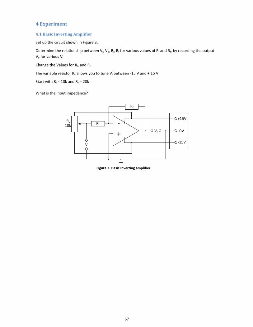
67
4 Experiment
4.1 Basic Inverting Amplifier
Set up the circuit shown in Figure 3.
Determine the relationship between Vi, Vo, Ri, Rf for various values of Ri and Rf, by recording the output
Vo for various Vi
Change the Values for Ri, and Rf
The variable resistor Rv allows you to tune Vi between -15 V and + 15 V
Start with Ri = 10k and Rf = 20k
What is the input impedance?
Figure 3. Basic Inverting amplifier
-
+
Ri
Rf
Rv
10k
Vi
Vo
+15V
0V
-15V
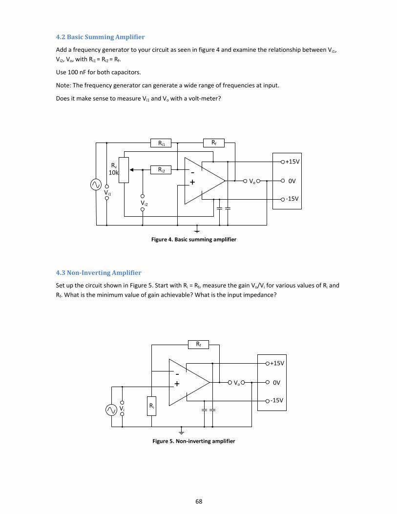
68
+ -
Rf
Vo
+15V
0V
-15V
Vi Ri
4.2 Basic Summing Amplifier
Add a frequency generator to your circuit as seen in figure 4 and examine the relationship between Vi1,
Vi2, Vo, with Ri1 = Ri2 = Rf.
Use 100 nF for both capacitors.
Note: The frequency generator can generate a wide range of frequencies at input.
Does it make sense to measure Vi1 and Vo with a volt-meter?
4.3 Non-Inverting Amplifier
Set up the circuit shown in Figure 5. Start with Ri = Rf, measure the gain Vo/Vi for various values of Ri and
Rf. What is the minimum value of gain achievable? What is the input impedance?
+ - Ri2
Rf
Rv
10k
Vi2
Vo
+15V
0V
-15V
Ri1
Vi1
Figure 4. Basic summing amplifier
Figure 5. Non-inverting amplifier
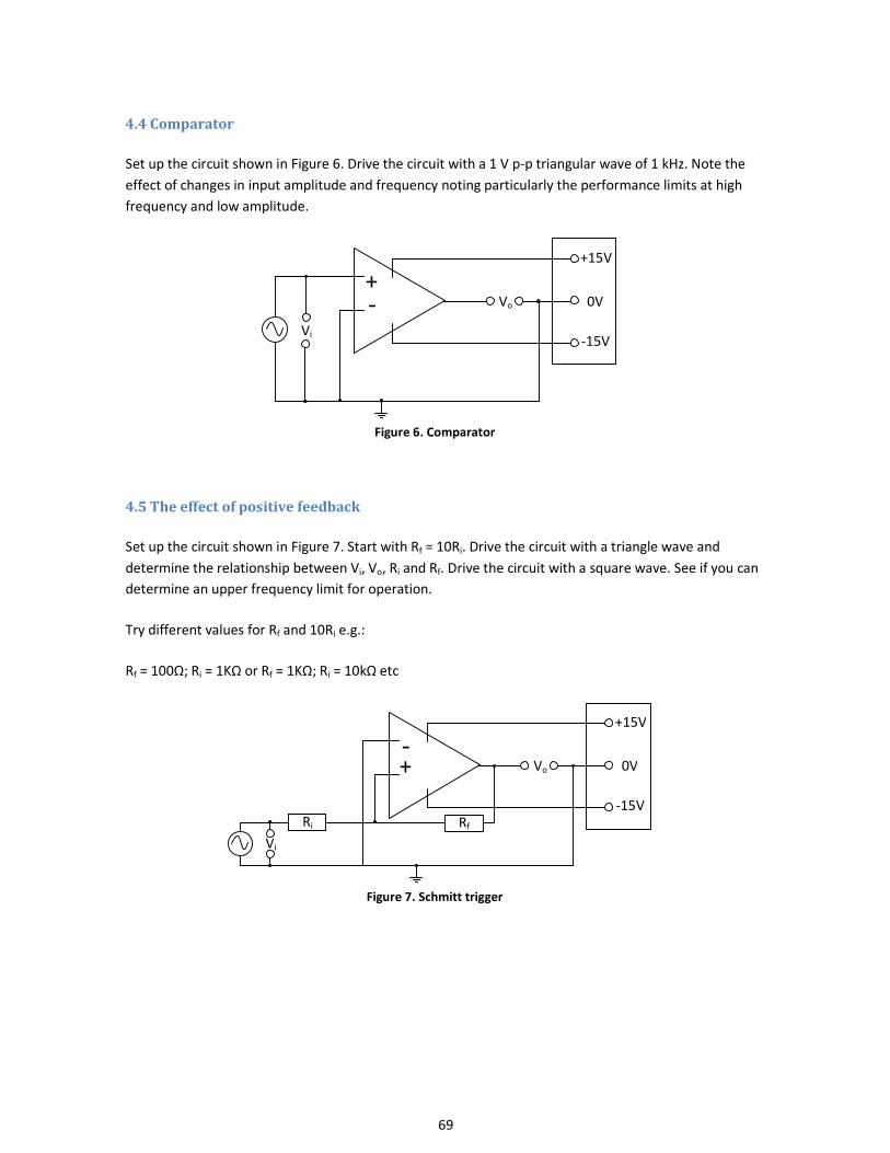
69
4.4 Comparator
Set up the circuit shown in Figure 6. Drive the circuit with a 1 V p-p triangular wave of 1 kHz. Note the
effect of changes in input amplitude and frequency noting particularly the performance limits at high
frequency and low amplitude.
4.5 The effect of positive feedback
Set up the circuit shown in Figure 7. Start with Rf = 10Ri. Drive the circuit with a triangle wave and
determine the relationship between Vi, Vo, Ri and Rf. Drive the circuit with a square wave. See if you can
determine an upper frequency limit for operation.
Try different values for Rf and 10Ri e.g.:
Rf = 100Ω; Ri = 1KΩ or Rf = 1KΩ; Ri = 10kΩ etc
+ - Vo
+15V
0V
-15V
Vi
+ -
Vo
+15V
0V
-15V
Vi
Ri Rf
Figure 6. Comparator
Figure 7. Schmitt trigger

70
Circuit Simulation with SPICE (Experiment C2)
Introduction
While the fundamental principles of electrical circuits are often exemplified by simple circuits containing
just a few elements, practical circuits are usually very complicated. Paper and pencil analysis, even with
the aid of a calculator, can only be applied to simple cases. Once the circuit exceeds more than a basic
level of complexity (say the order of ten elements and three or four independent sources), hand
calculations become tedious, prone to error and as the order of complexity increases, outright impossible.
Fortunately, computers can help us here, given suitable software.
SPICE is a well-known computer program for the 'simulation' of electrical circuits (that is, computer
calculation of the circuit equations, so that the computer 'circuit' behaves like the real one). SPICE covers
both AC and DC circuits, including semiconductor devices. It was originally developed at the University of
California, Berkeley, where continuing development has improved its accuracy and speed. It was not very
'user- friendly', and Berkeley allowed outside companies to incorporate it into more easily used interfaces,
both for input and output.
The aim of this experiment is to introduce the student to SPICE and to reinforce the subject matter
encountered in the Circuit Analysis module. This experiment restricts itself to DC circuit theory only.
It will be observed that the engineer may be presented with two broad tasks. The first may be called
"circuit analysis". A circuit of known arrangement, with components of known values, must be analysed
to identify various voltages and currents from which the circuit's performance may be identified. The
second task, and often the more practical one, is to design a circuit which will perform to a given set of
requirements, or specifications. This may be called "circuit synthesis" or "circuit implementation". While
the analysis usually has one specific set of solutions, synthesis will have several possible outcomes, the
choice being very much one of the designer's subjective judgement, based on experience. SPICE is
capable of being applied in both analysis and synthesis and is, therefore, a powerful tool. A later
experiment will involve applying SPICE to AC circuit design.
In this experiment, you will be asked to use SPICE to analyse a number of DC circuits of increasing
complexity. For some of the more simple cases you will also be asked to produce an answer by hand.
When you are competent with SPICE, you will then be able to apply it to a design problem.
About SPICE
To use SPICE you will need to use a text editor in order to input data. For this experiment, SPICE has been
installed on the PC's in the 1st Year Teaching Laboratory, using MicroSim PSpice® for Windows, version 8.
This comes with its own text editor, MicroSim Text Editor. This is very similar to Windows Notepad, but
you may need to familiarize yourself with it for a few minutes before doing the experiment.

71
The editor is used to provide SPICE with information about the circuit to be analysed. There are six
categories of information that will concern us in this experiment.
(a) Title line - any ASCII (basic text) string. The first line of the file must be a title line. It is ignored by the
calculating part of the simulator.
(a) Comments (these are optional) - any ASCII (basic text) string. A comment line must begin with a *
(asterisk). A comment can be added at the end of a program line, following a ; (semicolon).
(b) Labels - each circuit element has a label - the initial letter defines the component type - V for a voltage
source, R for a resistor etc.
(c) Node numbers - each node in the circuit must be numbered with only one number per node. A node is
any point on a conductor between two or more elements.
(d) Element values - the values of resistance, capacitance, voltage source etc. The SI unit after the value is
optional.
(e) Commands - give instructions to SPICE. Entered by starting with a full stop e.g. ‘.end’. Note that in
some versions of SPICE commands and labels need to be in upper case, but PSpice is not case-sensitive, so
use whichever makes the program most readable at that point.
A PSpice program consists of a set of statements. Each statement should occupy one line in the program
(if a statement exceeds one line, then it may continue on the next line preceded by a ‘+’). However, each
new statement must start on a new line. The program should be saved in a named file with the .cir
extension - e.g. fred.cir (when using the PSpice Text Editor the .cir extension is added automatically).
Actual Tasks
Ask your demonstrator how to find and launch the Design Manager and Text Editor programs on the PC
to perform the experiments.
Entering your program
In the Text Editor window, type in the text of your PSpice program (relating to ‘4. A First Example’ on the
next page). When this is complete, go to File, Save.
In the 'Save As' dialogue box you should be in a folder ‘Projects’ in D:\Msimev_8 (if not, navigate there).
Open a new folder inside Projects and give it your name or full initials as its name. (To open a new folder,
click the folder icon with the ‘sunrise’ on its top right corner. A new folder appears in the window,
selected. Just type your initials followed by pressing the 'Enter' key, and the folder name will be correct.)
Double click the folder icon to open it. Give the file a name, such as: dc1
Ensuring you are in your new folder, click the 'Save' button.

72
Click on the Design Manager window and then click the second icon down on the left hand side ('Run
PSpice AD'). A small window opens, headed 'PSpice AD'. In its 'File' menu, click 'Open'. Navigate to
your file and double-click it in the window.
A pop-up window will appear, either saying that your simulation has completed successfully, or telling
you that you have errors.
Close this pop-up window by clicking the 'OK' button.
In the 'File' menu, go to 'Examine output'. This- will open the output file, a text file, in the text editor.
This contains the original program, the results, and if there are errors, some information about them.
If there are errors, try to understand them, correct your program in the text editor, save it, and run
PSpice again. If you need help, ask the demonstrator.
When you have a successful run, edit your output file to remove unwanted space, blank lines, etc., to
give a readily legible file (the PSpice Text Editor has a 'Print Preview' feature under the File menu). Print
the file. If you bring scissors and glue, you can stick the results tidily in your logbook, which is the
desired outcome of the experiment.
You now need to program the other simulation files specified in the following sections, in the same way
as described above, and run each one in turn. Your aim is to become more familiar with the circuit
concepts involved, and with PSpice.
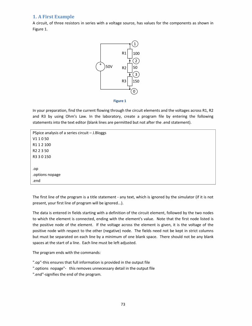
73
1. A First Example
A circuit, of three resistors in series with a voltage source, has values for the components as shown in
Figure 1.
In your preparation, find the current flowing through the circuit elements and the voltages across R1, R2
and R3 by using Ohm’s Law. In the laboratory, create a program file by entering the following
statements into the text editor (blank lines are permitted but not after the .end statement).
PSpice analysis of a series circuit – J.Bloggs
V1 1 0 50
R1 1 2 100
R2 2 3 50
R3 3 0 150
.op
.options nopage
.end
The first line of the program is a title statement - any text, which is ignored by the simulator (if it is not
present, your first line of program will be ignored...).
The data is entered in fields starting with a definition of the circuit element, followed by the two nodes
to which the element is connected, ending with the element's value. Note that the first node listed is
the positive node of the element. If the voltage across the element is given, it is the voltage of the
positive node with respect to the other (negative) node. The fields need not be kept in strict columns
but must be separated on each line by a minimum of one blank space. There should not be any blank
spaces at the start of a line. Each line must be left adjusted.
The program ends with the commands:
".op"-this ensures that full information is provided in the output file
".options nopage"- this removes unnecessary detail in the output file
".end"-signifies the end of the program.
+ 50V
R1
R2
R3
1
2
3
0
100
50
150
Figure 1

74
Save the program file, under a suitable name, for example dc1.cir, and then run PSpice by going to
PSpiceAD in the task bar at the bottom of the screen. Go to the File menu, and 'Open'. Navigate to your
.cir file and double-click.
An output file called e.g. dc1.out will be created. Examine this file, by going to the PSpiceAD File menu,
Examine Output. You are either looking for help on any errors, or to record the node voltages
calculated by PSpice. Compare these with your own answers. Also note the voltage source current.
[If you get an error message, "There are no devices in this circuit." you have probably put more than one
'Return' after the 'd' of '.end'. Another common error is to forget the title line and start the netlist on
line 1, which is then ignored by the simulator.]
The node voltages are all calculated with respect to "ground", that is node 0. Note also that the voltage
source current is given as negative. Can you suggest a reason for this? One further point about voltage
sources. The order of entering the nodes identifies the polarity i.e.
V1 1 0 50
is a voltage source of 50 V with the positive terminal connected to node 1.
V1 0 1 50
is a 50 V source with the positive terminal connected to node 0. Finally, dc1.out records the total power
dissipation in watts.
Edit the dc1.out file by removing unwanted blank lines. Print the file for your records (you will need
scissors and glue to stick the result in your log book).
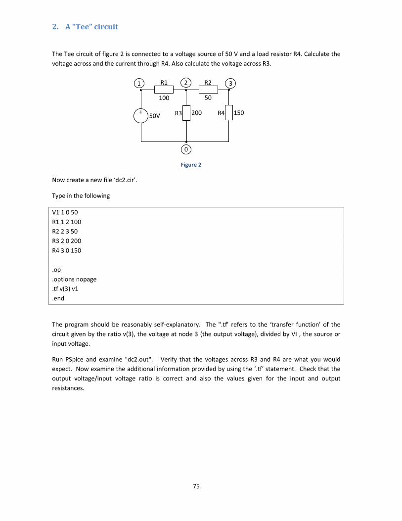
75
2. A “Tee” circuit
The Tee circuit of figure 2 is connected to a voltage source of 50 V and a load resistor R4. Calculate the
voltage across and the current through R4. Also calculate the voltage across R3.
Now create a new file ‘dc2.cir’.
Type in the following
V1 1 0 50
R1 1 2 100
R2 2 3 50
R3 2 0 200
R4 3 0 150
.op
.options nopage
.tf v(3) v1
.end
The program should be reasonably self-explanatory. The ".tf' refers to the ‘transfer function' of the
circuit given by the ratio v(3), the voltage at node 3 (the output voltage), divided by VI , the source or
input voltage.
Run PSpice and examine "dc2.out". Verify that the voltages across R3 and R4 are what you would
expect. Now examine the additional information provided by using the ‘.tf’ statement. Check that the
output voltage/input voltage ratio is correct and also the values given for the input and output
resistances.
+ 50V
R1 R2
R3
1 2 3
0
100 50
150 R4 200
Figure 2
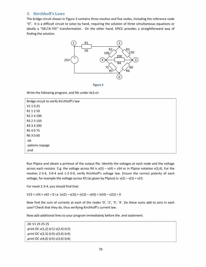
76
3. Kirchhoff’s Laws
The bridge circuit shown in Figure 3 contains three meshes and five nodes, including the reference node
"0". It is a difficult circuit to solve by hand, requiring the solution of three simultaneous equations or
ideally a "DELTA-TEE" transformation. On the other hand, SPICE provides a straightforward way of
finding the solution.
Write the following program, and file under dc3.cir.
Bridge circuit to verify Kirchhoff’s law
V1 1 0 25
R1 1 2 50
R2 2 4 100
R3 2 3 150
R4 3 4 200
R5 4 0 75
R6 3 0 60
.op
.options nopage
.end
Run PSpice and obtain a printout of the output file. Identify the voltages at each node and the voltage
across each resistor. E.g. the voltage across R4 is v(3) – v(4) = v34 or in PSpice notation v(3,4). For the
meshes 2-3-4, 3-0-4 and 1-2-3-0, verify Kirchhoff’s voltage law. Ensure the correct polarity of each
voltage, for example the voltage across R3 (as given by PSpice) is: v(2) – v(3) = v23.
For mesh 2-3-4, you should find that:
V23 + v34 + v42 = 0 i.e. v(2) – v(3) + v(3) – v(4) + v(4) – v(2) = 0
Now find the sum of currents at each of the nodes ‘0’, ‘2’, ‘3’, ‘4’. Do these sums add to zero in each
case? Check that they do, thus verifying Kirchhoff’s current law.
Now add additional lines to your program immediately before the .end statement:
.DC V1 25 25 25
.print DC v(1,2) i(r1) v(2,4) i(r2)
.print DC v(2,3) i(r3) v(3,4) i(r4)
.print DC v(4,0) i(r5) v(3,0) i(r6)
+ 25V
R1
R2 R3
1 2
3
0
50 100
R4
200 4
R5 R6
150
75 60
Figure 2
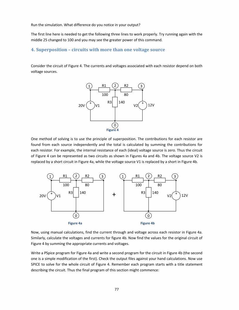
77
Run the simulation. What difference do you notice in your output?
The first line here is needed to get the following three lines to work properly. Try running again with the
middle 25 changed to 100 and you may see the greater power of this command.
4. Superposition – circuits with more than one voltage source
Consider the circuit of Figure 4. The currents and voltages associated with each resistor depend on both
voltage sources.
One method of solving is to use the principle of superposition. The contributions for each resistor are
found from each source independently and the total is calculated by summing the contributions for
each resistor. For example, the internal resistance of each (ideal) voltage source is zero. Thus the circuit
of Figure 4 can be represented as two circuits as shown in Figures 4a and 4b. The voltage source V2 is
replaced by a short circuit in Figure 4a, while the voltage source V1 is replaced by a short in Figure 4b.
Now, using manual calculations, find the current through and voltage across each resistor in Figure 4a.
Similarly, calculate the voltages and currents for figure 4b. Now find the values for the original circuit of
Figure 4 by summing the appropriate currents and voltages.
Write a PSpice program for Figure 4a and write a second program for the circuit in Figure 4b (the second
one is a simple modification of the first). Check the output files against your hand calculations. Now use
SPICE to solve for the whole circuit of Figure 4. Remember each program starts with a title statement
describing the circuit. Thus the final program of this section might commence:
0
+ 20V
R1 1
100
V1
R2
80
3
R3 140
2
0
R1 1
100
R2
80
+ 12V
3
R3 140 V2
2
+
Figure 4
0
+ 20V
R1 1
100
V1
R2
80
+ 12V
3
R3 140 V2
2
Figure 4a Figure 4b
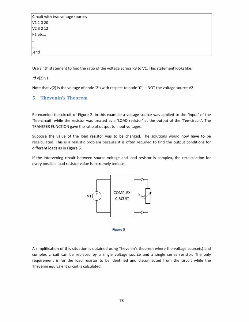
78
Circuit with two voltage sources
V1 1 0 20
V2 3 0 12
R1 etc...
...
...
.end
Use a ‘.tf’ statement to find the ratio of the voltage across R3 to V1. This statement looks like:
.tf v(2) v1
Note that v(2) is the voltage of node ‘2’ (with respect to node ‘0’) – NOT the voltage source V2.
5. Thevenin’s Theorem
Re-examine the circuit of Figure 2. In this example a voltage source was applied to the ‘input’ of the
‘Tee-circuit’ while the resistor was treated as a ‘LOAD resistor’ at the output of the ‘Tee-circuit’. The
TRANSFER FUNCTION gave the ratio of output to input voltages.
Suppose the value of the load resistor was to be changed. The solutions would now have to be
recalculated. This is a realistic problem because it is often required to find the output conditions for
different loads as in Figure 5.
If the intervening circuit between source voltage and load resistor is complex, the recalculation for
every possible load resistor value is extremely tedious.
A simplification of this situation is obtained using Thevenin’s theorem where the voltage source(s) and
complex circuit can be replaced by a single voltage source and a single series resistor. The only
requirement is for the load resistor to be identified and disconnected from the circuit while the
Thevenin equivalent circuit is calculated.
COMPLEX
CIRCUIT RLoad +
V1
Figure 5
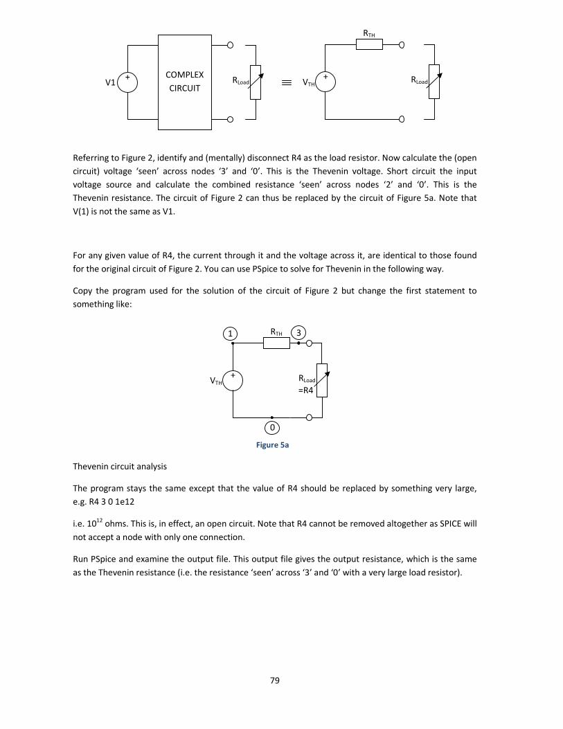
79
Referring to Figure 2, identify and (mentally) disconnect R4 as the load resistor. Now calculate the (open
circuit) voltage ‘seen’ across nodes ‘3’ and ‘0’. This is the Thevenin voltage. Short circuit the input
voltage source and calculate the combined resistance ‘seen’ across nodes ‘2’ and ‘0’. This is the
Thevenin resistance. The circuit of Figure 2 can thus be replaced by the circuit of Figure 5a. Note that
V(1) is not the same as V1.
For any given value of R4, the current through it and the voltage across it, are identical to those found
for the original circuit of Figure 2. You can use PSpice to solve for Thevenin in the following way.
Copy the program used for the solution of the circuit of Figure 2 but change the first statement to
something like:
Thevenin circuit analysis
The program stays the same except that the value of R4 should be replaced by something very large,
e.g. R4 3 0 1e12
i.e. 1012
ohms. This is, in effect, an open circuit. Note that R4 cannot be removed altogether as SPICE will
not accept a node with only one connection.
Run PSpice and examine the output file. This output file gives the output resistance, which is the same
as the Thevenin resistance (i.e. the resistance ‘seen’ across ‘3’ and ‘0’ with a very large load resistor).
RTH
COMPLEX
CIRCUIT RLoad +
V1 RLoad + VTH
0
=R4
3 1 RTH
RLoad + VTH
Figure 5a
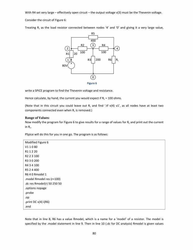
80
With R4 set very large – effectively open circuit – the output voltage v(3) must be the Thevenin voltage.
Consider the circuit of Figure 6:
Treating RL as the load resistor connected between nodes ‘4’ and ‘0’ and giving it a very large value,
write a SPICE program to find the Thevenin voltage and resistance.
Hence calculate, by hand, the current you would expect if RL = 100 ohms.
(Note that in this circuit you could leave out RL and find ‘.tf v(4) v1’, as all nodes have at least two
components connected even when RL is removed.)
Range of Values:
Now modify the program for Figure 6 to give results for a range of values for RL and print out the current
in RL.
PSpice will do this for you in one go. The program is as follows:
Modified Figure 6
V1 1 0 80
R1 1 2 20
R2 2 3 100
R3 3 0 200
R4 3 4 100
R5 2 4 400
R6 4 0 Rmodel 1
.model Rmodel res (r=100)
.dc res Rmodel(r) 50 250 50
.options nopage
.probe
.op
.print DC v(4) i(R6)
.end
Note that in line 8, R6 has a value Rmodel, which is a name for a ‘model’ of a resistor. The model is
specified by the .model statement in line 9. Then in line 10 (.dc for DC analysis) Rmodel is given values
+
R2 R4
R3 1
3 4
0
100 100
RL R6 200
80V
R1 20
R5
400
2
Figure 6
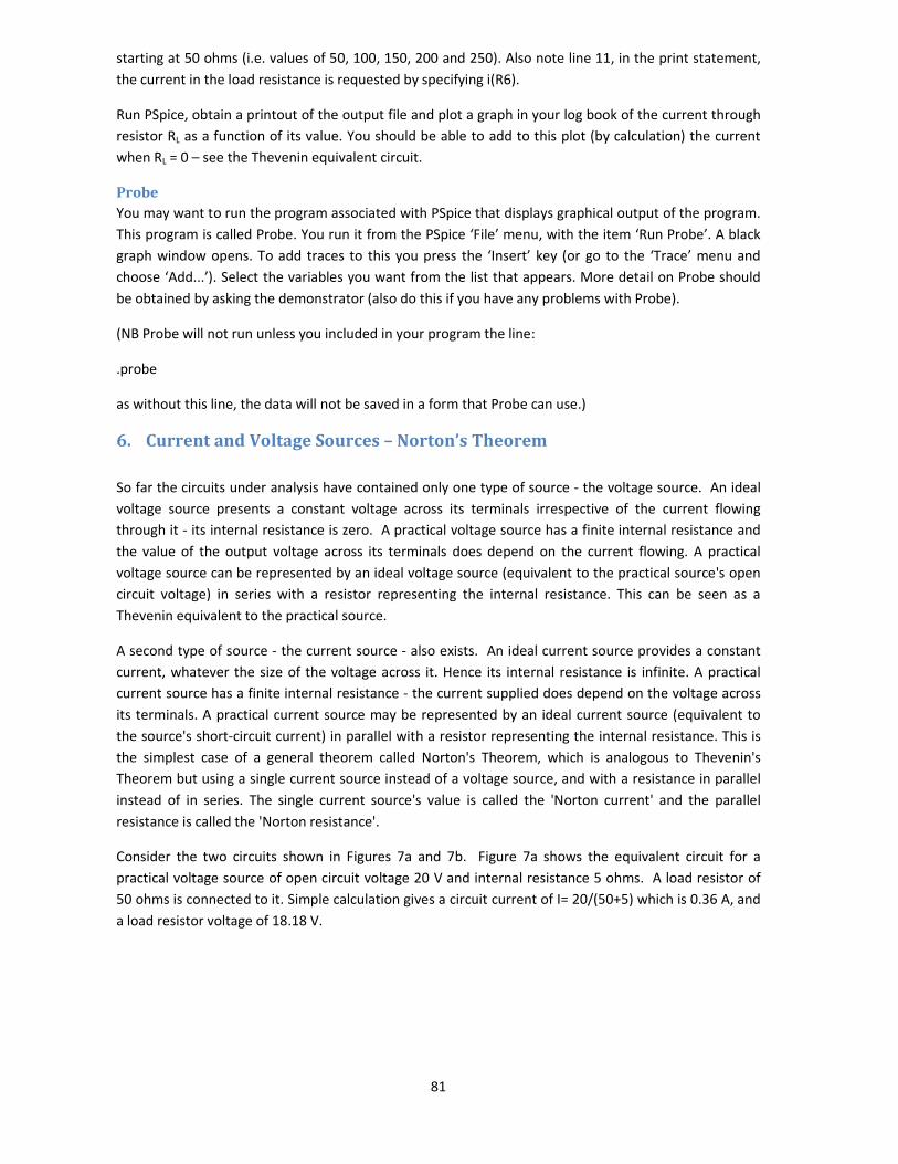
81
starting at 50 ohms (i.e. values of 50, 100, 150, 200 and 250). Also note line 11, in the print statement,
the current in the load resistance is requested by specifying i(R6).
Run PSpice, obtain a printout of the output file and plot a graph in your log book of the current through
resistor RL as a function of its value. You should be able to add to this plot (by calculation) the current
when RL = 0 – see the Thevenin equivalent circuit.
Probe
You may want to run the program associated with PSpice that displays graphical output of the program.
This program is called Probe. You run it from the PSpice ‘File’ menu, with the item ‘Run Probe’. A black
graph window opens. To add traces to this you press the ‘Insert’ key (or go to the ‘Trace’ menu and
choose ‘Add...’). Select the variables you want from the list that appears. More detail on Probe should
be obtained by asking the demonstrator (also do this if you have any problems with Probe).
(NB Probe will not run unless you included in your program the line:
.probe
as without this line, the data will not be saved in a form that Probe can use.)
6. Current and Voltage Sources – Norton’s Theorem
So far the circuits under analysis have contained only one type of source - the voltage source. An ideal
voltage source presents a constant voltage across its terminals irrespective of the current flowing
through it - its internal resistance is zero. A practical voltage source has a finite internal resistance and
the value of the output voltage across its terminals does depend on the current flowing. A practical
voltage source can be represented by an ideal voltage source (equivalent to the practical source's open
circuit voltage) in series with a resistor representing the internal resistance. This can be seen as a
Thevenin equivalent to the practical source.
A second type of source - the current source - also exists. An ideal current source provides a constant
current, whatever the size of the voltage across it. Hence its internal resistance is infinite. A practical
current source has a finite internal resistance - the current supplied does depend on the voltage across
its terminals. A practical current source may be represented by an ideal current source (equivalent to
the source's short-circuit current) in parallel with a resistor representing the internal resistance. This is
the simplest case of a general theorem called Norton's Theorem, which is analogous to Thevenin's
Theorem but using a single current source instead of a voltage source, and with a resistance in parallel
instead of in series. The single current source's value is called the 'Norton current' and the parallel
resistance is called the 'Norton resistance'.
Consider the two circuits shown in Figures 7a and 7b. Figure 7a shows the equivalent circuit for a
practical voltage source of open circuit voltage 20 V and internal resistance 5 ohms. A load resistor of
50 ohms is connected to it. Simple calculation gives a circuit current of I= 20/(50+5) which is 0.36 A, and
a load resistor voltage of 18.18 V.
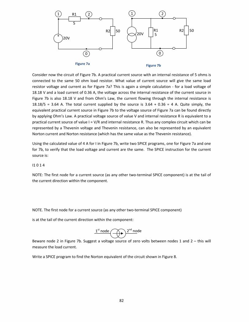
82
Consider now the circuit of Figure 7b. A practical current source with an internal resistance of 5 ohms is
connected to the same 50 ohm load resistor. What value of current source will give the same load
resistor voltage and current as for Figure 7a? This is again a simple calculation - for a load voltage of
18.18 V and a load current of 0.36 A, the voltage across the internal resistance of the current source in
Figure 7b is also 18.18 V and from Ohm’s Law, the current flowing through the internal resistance is
18.18/5 = 3.64 A. The total current supplied by the source is 3.64 + 0.36 = 4 A. Quite simply, the
equivalent practical current source in Figure 7b to the voltage source of Figure 7a can be found directly
by applying Ohm’s Law. A practical voltage source of value V and internal resistance R is equivalent to a
practical current source of value I = V/R and internal resistance R. Thus any complex circuit which can be
represented by a Thevenin voltage and Thevenin resistance, can also be represented by an equivalent
Norton current and Norton resistance (which has the same value as the Thevenin resistance).
Using the calculated value of 4 A for I in Figure 7b, write two SPICE programs, one for Figure 7a and one
for 7b, to verify that the load voltage and current are the same. The SPICE instruction for the current
source is:
I1 0 1 4
NOTE: The first node for a current source (as any other two-terminal SPICE component) is at the tail of
the current direction within the component.
NOTE. The first node for a current source (as any other two-terminal SPICE component)
is at the tail of the current direction within the component:
Beware node 2 in Figure 7b. Suggest a voltage source of zero volts between nodes 1 and 2 – this will
measure the load current.
Write a SPICE program to find the Norton equivalent of the circuit shown in Figure 8.
+
1
0
50 R2
20V
R1
5
2 1
0
50 R2 20V
R1 5
2
1st
node 2nd
node
Figure 7a Figure 7b
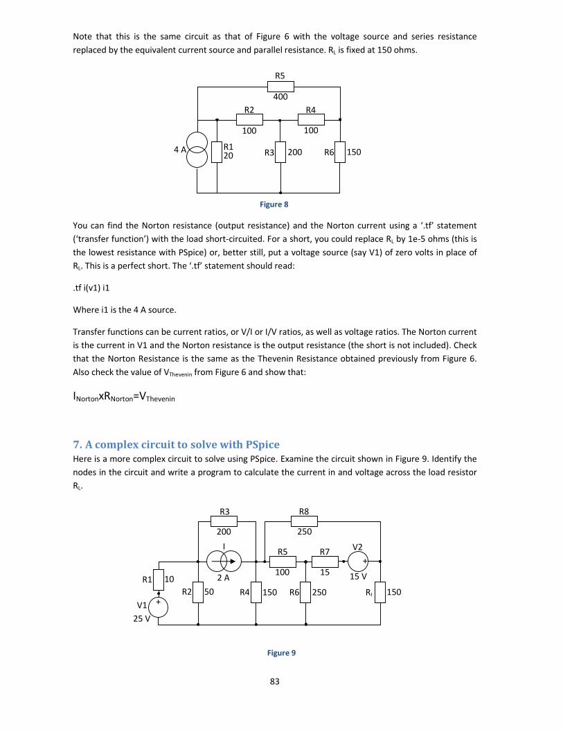
83
Note that this is the same circuit as that of Figure 6 with the voltage source and series resistance
replaced by the equivalent current source and parallel resistance. RL is fixed at 150 ohms.
You can find the Norton resistance (output resistance) and the Norton current using a ‘.tf’ statement
(‘transfer function’) with the load short-circuited. For a short, you could replace RL by 1e-5 ohms (this is
the lowest resistance with PSpice) or, better still, put a voltage source (say V1) of zero volts in place of
RL. This is a perfect short. The ‘.tf’ statement should read:
.tf i(v1) i1
Where i1 is the 4 A source.
Transfer functions can be current ratios, or V/I or I/V ratios, as well as voltage ratios. The Norton current
is the current in V1 and the Norton resistance is the output resistance (the short is not included). Check
that the Norton Resistance is the same as the Thevenin Resistance obtained previously from Figure 6.
Also check the value of VThevenin from Figure 6 and show that:
INortonxRNorton=VThevenin
7. A complex circuit to solve with PSpice
Here is a more complex circuit to solve using PSpice. Examine the circuit shown in Figure 9. Identify the
nodes in the circuit and write a program to calculate the current in and voltage across the load resistor
RL.
R2 R4
R3
100 100
R6 200 4 A R1 20
R5
400
150
R1
+
+
R2
R3
R4
R5
R6
R7
R8
RL
V1
V2 I
25 V
10
50 150 250 150
200
2 A 15 100 15 V
250
Figure 8
Figure 9
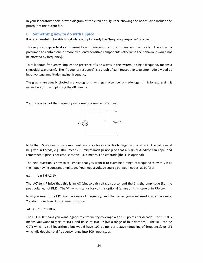
84
In your laboratory book, draw a diagram of the circuit of Figure 9, showing the nodes. Also include the
printout of the output file.
8. Something new to do with PSpice
It is often useful to be able to calculate and plot easily the "frequency response" of a circuit.
This requires PSpice to do a different type of analysis from the DC analysis used so far. The circuit is
presumed to contain one or more frequency-sensitive components (otherwise the behaviour would not
be affected by frequency).
To talk about 'frequency' implies the presence of sine waves in the system (a single frequency means a
sinusoidal waveform). The 'frequency response' is a graph of gain (output voltage amplitude divided by
input voltage amplitude) against frequency.
The graphs are usually plotted in a log-log form, with gain often being made logarithmic by expressing it
in decibels (dB), and plotting the dB linearly.
Your task is to plot the frequency response of a simple R-C circuit:
Note that PSpice needs the component reference for a capacitor to begin with a letter C. The value must
be given in Farads, e.g. 10uF means 10 microfarads [u not µ so that a plain text editor can cope, and
remember PSpice is not case-sensitive], 47p means 47 picofarads (the 'F' is optional).
The next question is how to tell PSpice that you want it to examine a range of frequencies, with Vin as
the input having constant amplitude. You need a voltage source between nodes, as before:
e.g. Vin 5 6 AC 1V
The 'AC' tells PSpice that this is an AC (sinusoidal) voltage source, and the 1 is the amplitude (i.e. the
peak voltage, not RMS). The 'V', which stands for volts, is optional (as are units in general in PSpice).
Now you need to tell PSpice the range of frequency, and the values you want used inside the range.
You do this with an .AC statement, such as:
.AC DEC 100 10 100k
The DEC 100 means you want logarithmic frequency coverage with 100 points per decade. The 10 100k
means you want to start at 10Hz and finish at 100kHz (NB a range of four decades). The DEC can be
OCT; which is still logarithmic but would have 100 points per octave (doubling of frequency), or LIN
which divides the total frequency range into 100 linear steps.
Vout VIN

85
You need the .PROBE statement to pass the data to PROBE for plotting.
When choosing values for your circuit you should select values of R and C which will give you a time
constant of 16μs.
Plot both the gain in dB and the phase in degrees against frequency, with the frequency scale set to
logarithmic. [In PROBE the phase of a voltage V(4) is specified as VP(4) when adding a trace]. Suggest
you start with a frequency range of 100Hz to 1 MHz.
From the PROBE graph, calculate
1. the cut-off frequency in Hz
2. the slope of the straight part of the falling characteristic, in dB per decade and in dB per octave.
E.H.S. Chilton
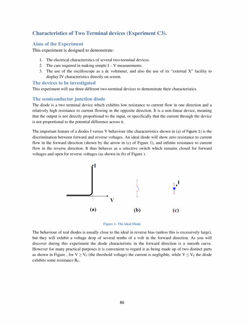
86
Characteristics of Two Terminal devices (Experiment C3).
Aims of the Experiment
This experiment is designed to demonstrate:
1. The electrical characteristics of several two-terminal devices.
2. The care required in making simple I – V measurements.
3. The use of the oscilloscope as a dc voltmeter, and also the use of its “external X” facility to
display IV characteristics directly on screen.
The devices to be investigated
This experiment will use three different two-terminal devices to demonstrate their characteristics.
The semiconductor junction diode
The diode is a two terminal device which exhibits low resistance to current flow in one direction and a
relatively high resistance to current flowing in the opposite direction. It is a non-linear device, meaning
that the output is not directly proportional to the input, or specifically that the current through the device
is not proportional to the potential difference across it.
The important feature of a diodes I versus V behaviour (the characteristics shown in (a) of Figure 1) is the
discrimination between forward and reverse voltages. An ideal diode will show zero resistance to current
flow in the forward direction (shown by the arrow in (c) of Figure 1), and infinite resistance to current
flow in the reverse direction. It thus behaves as a selective switch which remains closed for forward
voltages and open for reverse voltages (as shown in (b) of Figure ).
Figure 1- The ideal Diode
The behaviour of real diodes is usually close to the ideal in reverse bias (unless this is excessively large),
but they will exhibit a voltage drop of several tenths of a volt in the forward direction. As you will
discover during this experiment the diode characteristic in the forward direction is a smooth curve.
However for many practical purposes it is convenient to regard it as being made up of two distinct parts
as shown in Figure , for V ≥ VF (the threshold voltage) the current is negligible, while V ≤ VF the diode
exhibits some resistance RF.

Figure
The Photodiode
We have seen above that the single semiconductor
pass in one direction but not in the other according to the polarity of the applied voltage. Therefore it can
be regarded as a voltage controlled switch.
The photodiode has similar physical
mounted in such a way that light can fall onto an active area of the diode; Incident light generates
additional electrical charges (called holes and electrons) in the semiconductor. These ele
change the I-V characteristics. In the dark a photodiode exhibits much the same characteristics as a
conventional diode. However when illuminated the I
depends upon the intensity of illuminati
dependant switch.
The Zener Diode
This is another modified version of a conventional diode in that it is designed to operate in the reverse
bias state. Conventional diodes conduct very little cu
the reverse bias voltage is not too large (typically 50 to 2500v depending on type). If the reverse voltage
exceeds the maximum rated voltage then the junction of the diode begins to breakdown and consider
current is passed. This is referred to as the breakdown voltage. Zener diodes are designed to operate in
reverse bias, and have considerably lower breakdown voltages (typically 3 to 75v). They are also
engineered in such a way as to ensure very rapid
exceeded (Figure a). Zener diodes are only typically used in this reverse bias configuration
however exhibit similar characteristics as conventional diodes when operated in forward bias.
Figure 3 - Zener Diode symbol and I
Preparatory Work
As you may not have encountered all the devices described in this section you shoul
and undertake some background research into the three types of diode described. Make sure that you are
87
Figure 2 - Typical diode characteristics
We have seen above that the single semiconductor diode behaves as a simple switch, allowing current to
pass in one direction but not in the other according to the polarity of the applied voltage. Therefore it can
be regarded as a voltage controlled switch.
The photodiode has similar physical construction to a conventional diode but unlike the latter it is
mounted in such a way that light can fall onto an active area of the diode; Incident light generates
additional electrical charges (called holes and electrons) in the semiconductor. These ele
V characteristics. In the dark a photodiode exhibits much the same characteristics as a
conventional diode. However when illuminated the I-V characteristics are altered to an extent that
depends upon the intensity of illumination. In this respect the photodiode can be regarded as a light
This is another modified version of a conventional diode in that it is designed to operate in the reverse
bias state. Conventional diodes conduct very little current when operated in reverse bias, provided that
the reverse bias voltage is not too large (typically 50 to 2500v depending on type). If the reverse voltage
exceeds the maximum rated voltage then the junction of the diode begins to breakdown and consider
current is passed. This is referred to as the breakdown voltage. Zener diodes are designed to operate in
reverse bias, and have considerably lower breakdown voltages (typically 3 to 75v). They are also
engineered in such a way as to ensure very rapid increase in reverse current as the breakdown voltage is
a). Zener diodes are only typically used in this reverse bias configuration
however exhibit similar characteristics as conventional diodes when operated in forward bias.
Zener Diode symbol and I-V characteristic
As you may not have encountered all the devices described in this section you should study these notes
and undertake some background research into the three types of diode described. Make sure that you are
diode behaves as a simple switch, allowing current to
pass in one direction but not in the other according to the polarity of the applied voltage. Therefore it can
construction to a conventional diode but unlike the latter it is
mounted in such a way that light can fall onto an active area of the diode; Incident light generates
additional electrical charges (called holes and electrons) in the semiconductor. These electrical charges
V characteristics. In the dark a photodiode exhibits much the same characteristics as a
V characteristics are altered to an extent that
on. In this respect the photodiode can be regarded as a light
This is another modified version of a conventional diode in that it is designed to operate in the reverse
rrent when operated in reverse bias, provided that
the reverse bias voltage is not too large (typically 50 to 2500v depending on type). If the reverse voltage
exceeds the maximum rated voltage then the junction of the diode begins to breakdown and considerable
current is passed. This is referred to as the breakdown voltage. Zener diodes are designed to operate in
reverse bias, and have considerably lower breakdown voltages (typically 3 to 75v). They are also
increase in reverse current as the breakdown voltage is
a). Zener diodes are only typically used in this reverse bias configuration but do
however exhibit similar characteristics as conventional diodes when operated in forward bias.
d study these notes
and undertake some background research into the three types of diode described. Make sure that you are
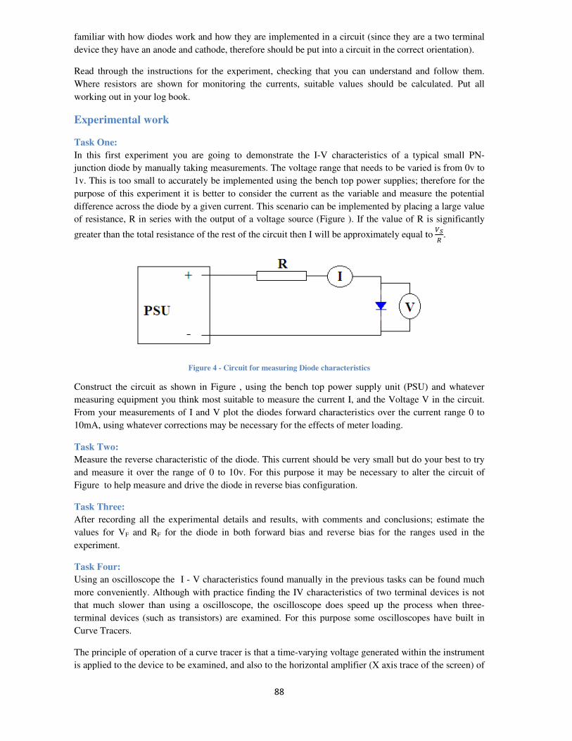
familiar with how diodes work and how they are implemented in a circuit (since they are a two terminal
device they have an anode and cathode, therefore should be put into a circuit in the correct orientation).
Read through the instructions for the experiment, checking that you can understand and follow them.
Where resistors are shown for monitoring the currents, suitable values should b
working out in your log book.
Experimental work
Task One:
In this first experiment you are going to demonstrate the I
junction diode by manually taking measurements. The voltage range that needs
1v. This is too small to accurately be implemented using the bench top power supplies; therefore for the
purpose of this experiment it is better to consider the current as the variable and measure the potential
difference across the diode by a given current. This scenario can be implemented by placing a large value
of resistance, R in series with the output of a voltage source (
greater than the total resistance of the rest of the circuit then I will be approximately equal to
Figure 4 - Circuit for measuring Diode characteristics
Construct the circuit as shown in Figure
measuring equipment you think most suitable to measure the current I, and the Voltage
From your measurements of I and V plot the diodes forward characteristics over the current range 0 to
10mA, using whatever corrections may be necessary for the effects of meter loading.
Task Two:
Measure the reverse characteristic of the
and measure it over the range of 0 to 10v. For this purpose it may be necessary to alter the circuit of
Figure to help measure and drive the diode in reverse bias configuration.
Task Three:
After recording all the experimental details and results, with comments and conclusions; estimate the
values for VF and RF for the diode in both forward bias and reverse bias for the ranges used in the
experiment.
Task Four:
Using an oscilloscope the I - V characteristics found manually in the previous tasks can be found much
more conveniently. Although with practice finding
that much slower than using a oscilloscope
terminal devices (such as transistors) are examined. For this purpose some oscilloscopes have built in
Curve Tracers.
The principle of operation of a curve tracer is that a time
is applied to the device to be examined, and also to the horizontal amplifier (X axis trace of the screen) of
88
familiar with how diodes work and how they are implemented in a circuit (since they are a two terminal
cathode, therefore should be put into a circuit in the correct orientation).
Read through the instructions for the experiment, checking that you can understand and follow them.
Where resistors are shown for monitoring the currents, suitable values should be calculated. Put all
In this first experiment you are going to demonstrate the I-V characteristics of a typical small PN
junction diode by manually taking measurements. The voltage range that needs to be varied is from 0v to
1v. This is too small to accurately be implemented using the bench top power supplies; therefore for the
purpose of this experiment it is better to consider the current as the variable and measure the potential
the diode by a given current. This scenario can be implemented by placing a large value
of resistance, R in series with the output of a voltage source (Figure ). If the value of R is significantly
greater than the total resistance of the rest of the circuit then I will be approximately equal to
Circuit for measuring Diode characteristics
Figure , using the bench top power supply unit (PSU) and whatever
measuring equipment you think most suitable to measure the current I, and the Voltage V in the circuit.
From your measurements of I and V plot the diodes forward characteristics over the current range 0 to
10mA, using whatever corrections may be necessary for the effects of meter loading.
Measure the reverse characteristic of the diode. This current should be very small but do your best to try
and measure it over the range of 0 to 10v. For this purpose it may be necessary to alter the circuit of
to help measure and drive the diode in reverse bias configuration.
After recording all the experimental details and results, with comments and conclusions; estimate the
for the diode in both forward bias and reverse bias for the ranges used in the
V characteristics found manually in the previous tasks can be found much
more conveniently. Although with practice finding the IV characteristics of two terminal devices is not
oscilloscope, the oscilloscope does speed up the process when three
terminal devices (such as transistors) are examined. For this purpose some oscilloscopes have built in
The principle of operation of a curve tracer is that a time-varying voltage generated within the instrument
is applied to the device to be examined, and also to the horizontal amplifier (X axis trace of the screen) of
familiar with how diodes work and how they are implemented in a circuit (since they are a two terminal
cathode, therefore should be put into a circuit in the correct orientation).
Read through the instructions for the experiment, checking that you can understand and follow them.
e calculated. Put all
V characteristics of a typical small PN-
to be varied is from 0v to
1v. This is too small to accurately be implemented using the bench top power supplies; therefore for the
purpose of this experiment it is better to consider the current as the variable and measure the potential
the diode by a given current. This scenario can be implemented by placing a large value
). If the value of R is significantly
greater than the total resistance of the rest of the circuit then I will be approximately equal to 89: .
, using the bench top power supply unit (PSU) and whatever
V in the circuit.
From your measurements of I and V plot the diodes forward characteristics over the current range 0 to
diode. This current should be very small but do your best to try
and measure it over the range of 0 to 10v. For this purpose it may be necessary to alter the circuit of
After recording all the experimental details and results, with comments and conclusions; estimate the
for the diode in both forward bias and reverse bias for the ranges used in the
V characteristics found manually in the previous tasks can be found much
the IV characteristics of two terminal devices is not
does speed up the process when three-
terminal devices (such as transistors) are examined. For this purpose some oscilloscopes have built in
varying voltage generated within the instrument
is applied to the device to be examined, and also to the horizontal amplifier (X axis trace of the screen) of
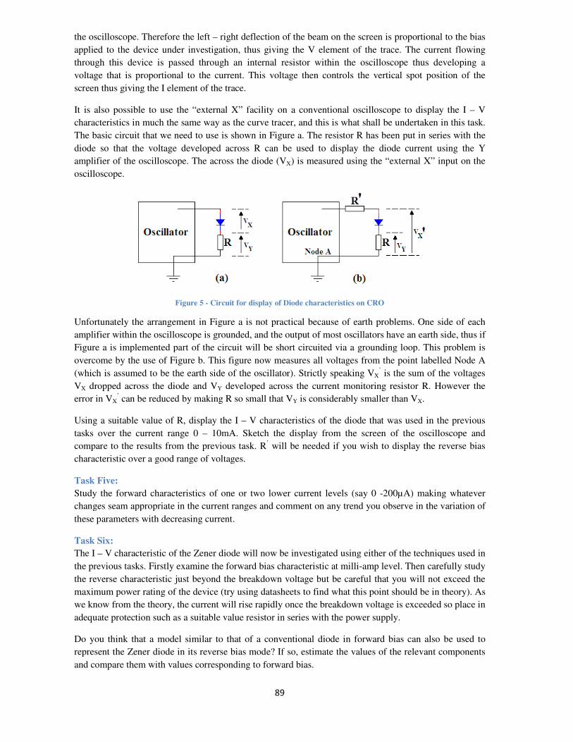
the oscilloscope. Therefore the left – right deflection of the beam on the screen is proportional to the bias
applied to the device under investigation, thus giving the V element of the trace. The current flowing
through this device is passed through an internal resistor within
voltage that is proportional to the current. This voltage then controls the vertical spot position of the
screen thus giving the I element of the trace.
It is also possible to use the “external X” facility on a conventio
characteristics in much the same way as the curve tracer, and this is what shall be undertaken in this task.
The basic circuit that we need to use is shown in
diode so that the voltage developed across R can be used to display the diode current using the Y
amplifier of the oscilloscope. The across the diode (V
oscilloscope.
Figure 5 - Circuit for display of Diode characteristics on CRO
Unfortunately the arrangement in Figure
amplifier within the oscilloscope is grounded, and the output of most oscillators have an earth side, thus if
Figure a is implemented part of the circuit will be short circuited via a grounding loop. This problem is
overcome by the use of Figure b. This figure now measures all voltages from the point labelled Node A
(which is assumed to be the earth side of the oscillator). Strictly speaking V
VX dropped across the diode and VY developed across the current monitoring resistor R. However the
error in VX’ can be reduced by making R so small that V
Using a suitable value of R, display the I
tasks over the current range 0 – 10mA. Sketch the display from the screen of the
compare to the results from the previous task. R
characteristic over a good range of voltages.
Task Five:
Study the forward characteristics of one or two lower current levels (say 0
changes seam appropriate in the current ranges and comment on any trend you observe in the
these parameters with decreasing current.
Task Six:
The I – V characteristic of the Zener diode will now be investigated using either of the techniques used in
the previous tasks. Firstly examine the forward bias characteristic at milli
the reverse characteristic just beyond the breakdown voltage but be careful that you will not exceed the
maximum power rating of the device (try using datasheets to find what this point should be in theory). As
we know from the theory, the current will rise rapidly once the breakdown voltage is exceeded so place in
adequate protection such as a suitable value resistor in series with the power supply.
Do you think that a model similar to that of a conventional diode in forward bias
represent the Zener diode in its reverse bias mode? If so, estimate the values of the relevant components
and compare them with values corresponding to forward bias.
89
right deflection of the beam on the screen is proportional to the bias
applied to the device under investigation, thus giving the V element of the trace. The current flowing
through this device is passed through an internal resistor within the oscilloscope thus developing a
voltage that is proportional to the current. This voltage then controls the vertical spot position of the
screen thus giving the I element of the trace.
It is also possible to use the “external X” facility on a conventional oscilloscope to display the I
characteristics in much the same way as the curve tracer, and this is what shall be undertaken in this task.
The basic circuit that we need to use is shown in Figure a. The resistor R has been put in series with the
diode so that the voltage developed across R can be used to display the diode current using the Y
. The across the diode (VX) is measured using the “external X” input on the
Circuit for display of Diode characteristics on CRO
Figure a is not practical because of earth problems. One side of each
is grounded, and the output of most oscillators have an earth side, thus if
a is implemented part of the circuit will be short circuited via a grounding loop. This problem is
b. This figure now measures all voltages from the point labelled Node A
(which is assumed to be the earth side of the oscillator). Strictly speaking VX’ is the sum of the voltages
developed across the current monitoring resistor R. However the
can be reduced by making R so small that VY is considerably smaller than VX.
Using a suitable value of R, display the I – V characteristics of the diode that was used in the previous
10mA. Sketch the display from the screen of the oscilloscope
compare to the results from the previous task. R’ will be needed if you wish to display the reverse bia
characteristic over a good range of voltages.
Study the forward characteristics of one or two lower current levels (say 0 -200µA) making whatever
changes seam appropriate in the current ranges and comment on any trend you observe in the
these parameters with decreasing current.
V characteristic of the Zener diode will now be investigated using either of the techniques used in
the previous tasks. Firstly examine the forward bias characteristic at milli-amp level. Then carefully study
the reverse characteristic just beyond the breakdown voltage but be careful that you will not exceed the
maximum power rating of the device (try using datasheets to find what this point should be in theory). As
eory, the current will rise rapidly once the breakdown voltage is exceeded so place in
adequate protection such as a suitable value resistor in series with the power supply.
Do you think that a model similar to that of a conventional diode in forward bias can also be used to
represent the Zener diode in its reverse bias mode? If so, estimate the values of the relevant components
and compare them with values corresponding to forward bias.
right deflection of the beam on the screen is proportional to the bias
applied to the device under investigation, thus giving the V element of the trace. The current flowing
thus developing a
voltage that is proportional to the current. This voltage then controls the vertical spot position of the
to display the I – V
characteristics in much the same way as the curve tracer, and this is what shall be undertaken in this task.
a. The resistor R has been put in series with the
diode so that the voltage developed across R can be used to display the diode current using the Y
) is measured using the “external X” input on the
a is not practical because of earth problems. One side of each
is grounded, and the output of most oscillators have an earth side, thus if
a is implemented part of the circuit will be short circuited via a grounding loop. This problem is
b. This figure now measures all voltages from the point labelled Node A
of the voltages
developed across the current monitoring resistor R. However the
acteristics of the diode that was used in the previous
oscilloscope and
will be needed if you wish to display the reverse bias
200µA) making whatever
changes seam appropriate in the current ranges and comment on any trend you observe in the variation of
V characteristic of the Zener diode will now be investigated using either of the techniques used in
vel. Then carefully study
the reverse characteristic just beyond the breakdown voltage but be careful that you will not exceed the
maximum power rating of the device (try using datasheets to find what this point should be in theory). As
eory, the current will rise rapidly once the breakdown voltage is exceeded so place in
can also be used to
represent the Zener diode in its reverse bias mode? If so, estimate the values of the relevant components

90
Task Seven:
The photodiode will now be investigated. A small bulb (powered by a 1.5v source) may be used to
illuminate the active area of the photodiode. In order for this task to work the bulb needs to be placed
almost in contact with the photodiode.
With the bulb OFF display the characteristics of the photodiode on the oscilloscope as in previous tasks,
using a suitable value for R appropriate to a maximum current of approximately 10µA. Now illuminate
the diode using the bulb with a 2Ω resistor in series with the bulb. Keeping the voltage constant if a
battery not used repeat this with a 1Ω resistor in series and finally with no resistor. Sketch the waveforms
in your log book on a common set of axis. Can you attach any significance to the fact that the
characteristics pass through the fourth quadrant when the diode is illuminated?