Embed Size (px)
Citation preview
2111 Comprehensive Drive
Aurora, Illinois 60505
Phone: 630-851-4722
Fax: 630- 851- 5040
www.conwin.com
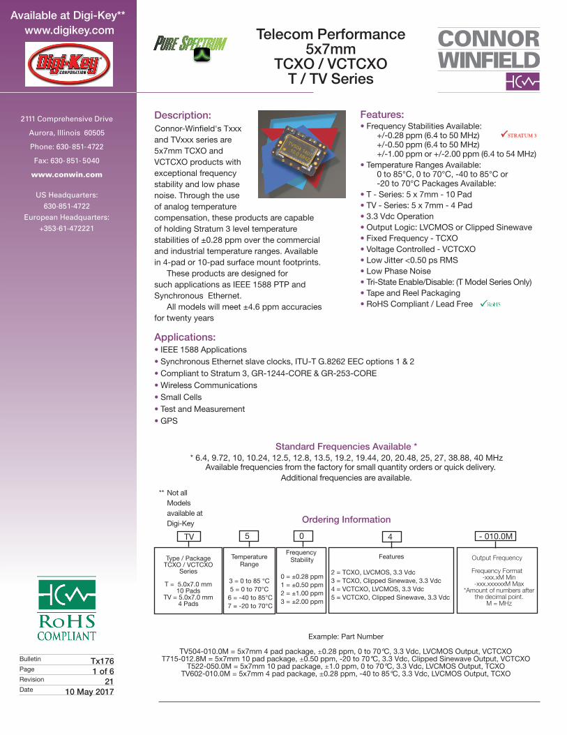
Telecom Performance5x7mm
TCXO / VCTCXOT / TV Series
Description:Connor-Winfield's Txxx and TVxxx series are 5x7mm TCXO and VCTCXO products with exceptional frequency stability and low phase noise. Through the use of analog temperature compensation, these products are capable of holding Stratum 3 level temperature stabilities of ±0.28 ppm over the commercial and industrial temperature ranges. Available in 4-pad or 10-pad surface mount footprints. These products are designed for such applications as IEEE 1588 PTP and Synchronous Ethernet. All models will meet ±4.6 ppm accuracies for twenty years
Features:• Frequency Stabilities Available: +/-0.28 ppm (6.4 to 50 MHz) +/-0.50 ppm (6.4 to 50 MHz) +/-1.00 ppm or +/-2.00 ppm (6.4 to 54 MHz)• Temperature Ranges Available: 0 to 85°C, 0 to 70°C, -40 to 85°C or -20 to 70°C Packages Available:• T - Series: 5 x 7mm - 10 Pad• TV - Series: 5 x 7mm - 4 Pad• 3.3 Vdc Operation• Output Logic: LVCMOS or Clipped Sinewave• Fixed Frequency - TCXO• Voltage Controlled - VCTCXO• Low Jitter <0.50 ps RMS• Low Phase Noise• Tri-State Enable/Disable: (T Model Series Only)• Tape and Reel Packaging• RoHS Compliant / Lead Free
Bulletin Tx176Page 1 of 6Revision 21Date 10 May 2017
US Headquarters:
630-851-4722
European Headquarters:
+353-61-472221
Type / PackageTCXO / VCTCXO
Series
T = 5.0x7.0 mm 10 Pads
TV = 5.0x7.0 mm 4 Pads
Output Frequency
Frequency Format -xxx.xM Min
-xxx.xxxxxxM Max*Amount of numbers after
the decimal point. M = MHz
TV - 010.0M
Ordering Information
Example: Part Number
TV504-010.0M = 5x7mm 4 pad package, ±0.28 ppm, 0 to 70°C, 3.3 Vdc, LVCMOS Output, VCTCXOT715-012.8M = 5x7mm 10 pad package, ±0.50 ppm, -20 to 70°C, 3.3 Vdc, Clipped Sinewave Output, VCTCXO
T522-050.0M = 5x7mm 10 pad package, ±1.0 ppm, 0 to 70°C, 3.3 Vdc, LVCMOS Output, TCXOTV602-010.0M = 5x7mm 4 pad package, ±0.28 ppm, -40 to 85°C, 3.3 Vdc, LVCMOS Output, TCXO
TV504 140710.0 MHZ
Features
2 = TCXO, LVCMOS, 3.3 Vdc 3 = TCXO, Clipped Sinewave, 3.3 Vdc 4 = VCTCXO, LVCMOS, 3.3 Vdc 5 = VCTCXO, Clipped Sinewave, 3.3 Vdc
Temperature Range
3 = 0 to 85 °C5 = 0 to 70°C
6 = -40 to 85°C 7 = -20 to 70°C
Frequency Stability
0 = ±0.28 ppm 1 = ±0.50 ppm 2 = ±1.00 ppm 3 = ±2.00 ppm
4 5 0
Standard Frequencies Available ** 6.4, 9.72, 10, 10.24, 12.5, 12.8, 13.5, 19.2, 19.44, 20, 20.48, 25, 27, 38.88, 40 MHz
Available frequencies from the factory for small quantity orders or quick delivery. Additional frequencies are available.
Applications:• IEEE 1588 Applications• Synchronous Ethernet slave clocks, ITU-T G.8262 EEC options 1 & 2• Compliant to Stratum 3, GR-1244-CORE & GR-253-CORE• Wireless Communications• Small Cells• Test and Measurement• GPS
Available at Digi-Key** www.digikey.com
** Not all Models available at Digi-Key
Specifications subject to change without notification. See Connor-Winfield's website for latest revision. © Copyright 2017 The Connor-Winfield Corporation Not intended for life support applications.
2111 Comprehensive Drive
Aurora, Illinois 60505
Phone: 630-851-4722
Fax: 630- 851- 5040
www.conwin.com
Bulletin Tx176Page 2 of 6Revision 21Date 10 May 2017
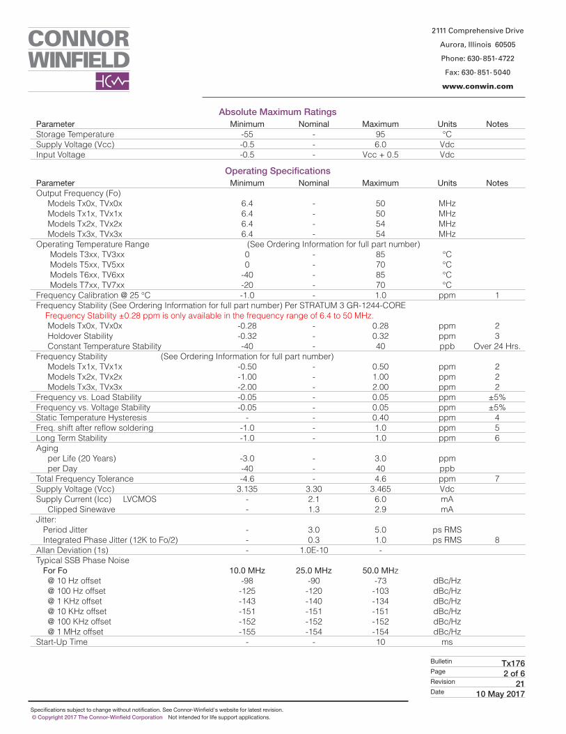
Operating SpecificationsParameter Minimum Nominal Maximum Units NotesOutput Frequency (Fo) Models Tx0x, TVx0x 6.4 - 50 MHz Models Tx1x, TVx1x 6.4 - 50 MHz Models Tx2x, TVx2x 6.4 - 54 MHz Models Tx3x, TVx3x 6.4 - 54 MHz Operating Temperature Range (See Ordering Information for full part number) Models T3xx, TV3xx 0 - 85 °C Models T5xx, TV5xx 0 - 70 °C Models T6xx, TV6xx -40 - 85 °C Models T7xx, TV7xx -20 - 70 °CFrequency Calibration @ 25 °C -1.0 - 1.0 ppm 1Frequency Stability (See Ordering Information for full part number) Per STRATUM 3 GR-1244-CORE Frequency Stability ±0.28 ppm is only available in the frequency range of 6.4 to 50 MHz. Models Tx0x, TVx0x -0.28 - 0.28 ppm 2 Holdover Stability -0.32 - 0.32 ppm 3 Constant Temperature Stability -40 - 40 ppb Over 24 Hrs.Frequency Stability (See Ordering Information for full part number) Models Tx1x, TVx1x -0.50 - 0.50 ppm 2 Models Tx2x, TVx2x -1.00 - 1.00 ppm 2 Models Tx3x, TVx3x -2.00 - 2.00 ppm 2Frequency vs. Load Stability -0.05 - 0.05 ppm ±5%Frequency vs. Voltage Stability -0.05 - 0.05 ppm ±5%Static Temperature Hysteresis - - 0.40 ppm 4Freq. shift after reflow soldering -1.0 - 1.0 ppm 5Long Term Stability -1.0 - 1.0 ppm 6Aging per Life (20 Years) -3.0 - 3.0 ppm per Day -40 - 40 ppbTotal Frequency Tolerance -4.6 - 4.6 ppm 7Supply Voltage (Vcc) 3.135 3.30 3.465 VdcSupply Current (Icc) LVCMOS - 2.1 6.0 mA Clipped Sinewave - 1.3 2.9 mAJitter: Period Jitter - 3.0 5.0 ps RMS Integrated Phase Jitter (12K to Fo/2) - 0.3 1.0 ps RMS 8Allan Deviation (1s) - 1.0E-10 -Typical SSB Phase Noise For Fo 10.0 MHz 25.0 MHz 50.0 MHz @ 10 Hz offset -98 -90 -73 dBc/Hz @ 100 Hz offset -125 -120 -103 dBc/Hz @ 1 KHz offset -143 -140 -134 dBc/Hz @ 10 KHz offset -151 -151 -151 dBc/Hz @ 100 KHz offset -152 -152 -152 dBc/Hz @ 1 MHz offset -155 -154 -154 dBc/HzStart-Up Time - - 10 ms
Absolute Maximum RatingsParameter Minimum Nominal Maximum Units NotesStorage Temperature -55 - 95 °CSupply Voltage (Vcc) -0.5 - 6.0 VdcInput Voltage -0.5 - Vcc + 0.5 Vdc
Specifications subject to change without notification. See Connor-Winfield's website for latest revision. © Copyright 2017 The Connor-Winfield Corporation Not intended for life support applications.
2111 Comprehensive Drive
Aurora, Illinois 60505
Phone: 630-851-4722
Fax: 630- 851- 5040
www.conwin.com
Bulletin Tx176Page 3 of 6Revision 21Date 10 May 2017
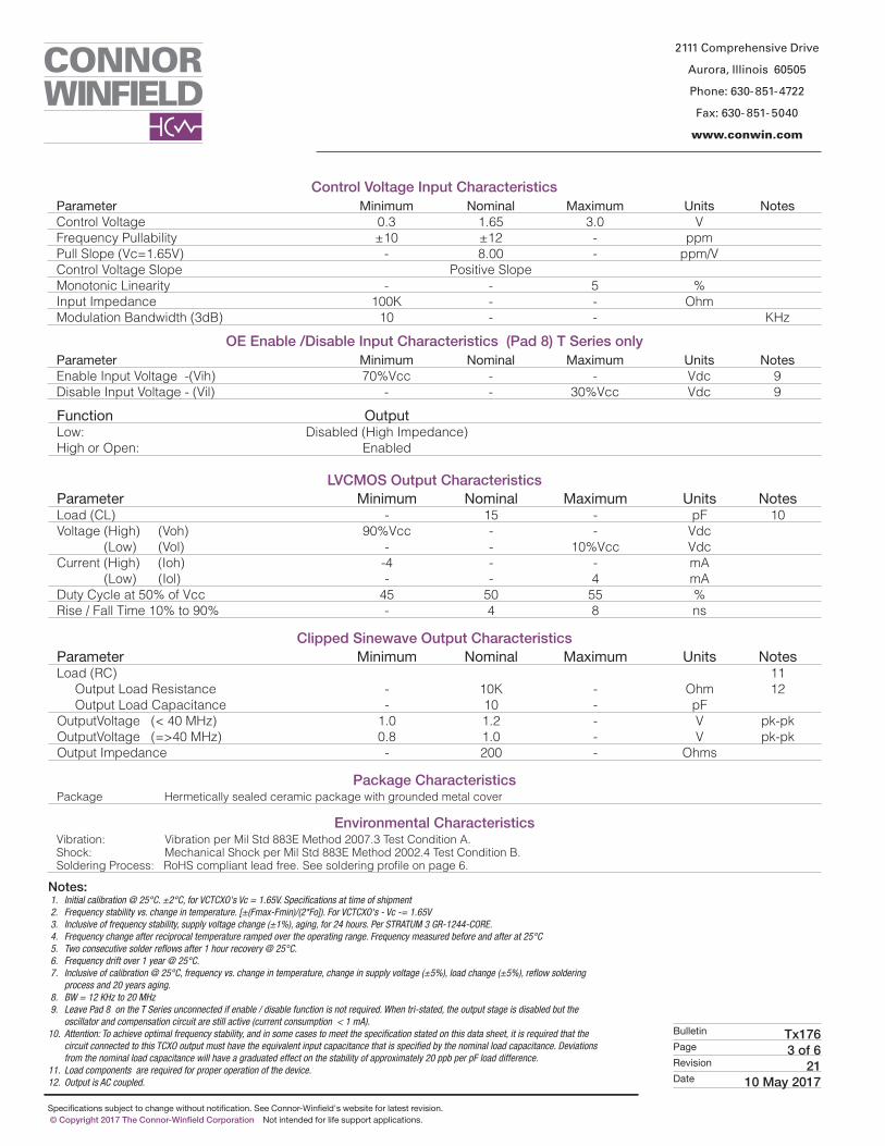
Environmental CharacteristicsVibration: Vibration per Mil Std 883E Method 2007.3 Test Condition A. Shock: Mechanical Shock per Mil Std 883E Method 2002.4 Test Condition B. Soldering Process: RoHS compliant lead free. See soldering profile on page 6.
Package CharacteristicsPackage Hermetically sealed ceramic package with grounded metal cover
Function OutputLow: Disabled (High Impedance) High or Open: Enabled
OE Enable /Disable Input Characteristics (Pad 8) T Series onlyParameter Minimum Nominal Maximum Units NotesEnable Input Voltage -(Vih) 70%Vcc - - Vdc 9Disable Input Voltage - (Vil) - - 30%Vcc Vdc 9
LVCMOS Output CharacteristicsParameter Minimum Nominal Maximum Units NotesLoad (CL) - 15 - pF 10Voltage (High) (Voh) 90%Vcc - - Vdc (Low) (Vol) - - 10%Vcc VdcCurrent (High) (Ioh) -4 - - mA (Low) (Iol) - - 4 mADuty Cycle at 50% of Vcc 45 50 55 %Rise / Fall Time 10% to 90% - 4 8 ns
Notes: 1. Initial calibration @ 25°C. ±2°C, for VCTCXO's Vc = 1.65V. Specifications at time of shipment 2. Frequency stability vs. change in temperature. [±(Fmax-Fmin)/(2*Fo]). For VCTCXO's - Vc -= 1.65V 3. Inclusive of frequency stability, supply voltage change (±1%), aging, for 24 hours. Per STRATUM 3 GR-1244-CORE. 4. Frequency change after reciprocal temperature ramped over the operating range. Frequency measured before and after at 25°C 5. Two consecutive solder reflows after 1 hour recovery @ 25°C. 6. Frequency drift over 1 year @ 25°C. 7. Inclusive of calibration @ 25°C, frequency vs. change in temperature, change in supply voltage (±5%), load change (±5%), reflow soldering process and 20 years aging. 8. BW = 12 KHz to 20 MHz 9. Leave Pad 8 on the T Series unconnected if enable / disable function is not required. When tri-stated, the output stage is disabled but the oscillator and compensation circuit are still active (current consumption < 1 mA).10. Attention: To achieve optimal frequency stability, and in some cases to meet the specification stated on this data sheet, it is required that the circuit connected to this TCXO output must have the equivalent input capacitance that is specified by the nominal load capacitance. Deviations from the nominal load capacitance will have a graduated effect on the stability of approximately 20 ppb per pF load difference.11. Load components are required for proper operation of the device. 12. Output is AC coupled.
Clipped Sinewave Output CharacteristicsParameter Minimum Nominal Maximum Units NotesLoad (RC) 11 Output Load Resistance - 10K - Ohm 12 Output Load Capacitance - 10 - pFOutput Voltage (< 40 MHz) 1.0 1.2 - V pk-pk Output Voltage (=>40 MHz) 0.8 1.0 - V pk-pkOutput Impedance - 200 - Ohms
Control Voltage Input CharacteristicsParameter Minimum Nominal Maximum Units NotesControl Voltage 0.3 1.65 3.0 V Frequency Pullability ±10 ±12 - ppmPull Slope (Vc=1.65V) - 8.00 - ppm/VControl Voltage Slope Positive Slope Monotonic Linearity - - 5 %Input Impedance 100K - - OhmModulation Bandwidth (3dB) 10 - - KHz
Specifications subject to change without notification. See Connor-Winfield's website for latest revision. © Copyright 2017 The Connor-Winfield Corporation Not intended for life support applications.
2111 Comprehensive Drive
Aurora, Illinois 60505
Phone: 630-851-4722
Fax: 630- 851- 5040
www.conwin.com
Bulletin Tx176Page 4 of 6Revision 21Date 10 May 2017
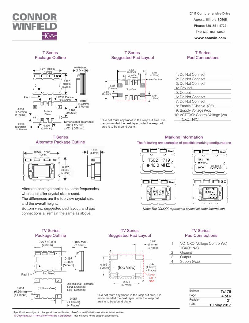
T Series Suggested Pad Layout
0.215(5.46mm)
0.037(0.94mm)
0.051(1.28mm)
0.051(1.28mm)
0.295(7.49mm)
0.030(0.76mm)
Keep Out Area
Top View
1
10
9 5
4
8
2 3
67
0.276 0.006(7.0mm)
±
0.1970.006
(5.0mm)±
0.079 Max.(2.0mm)
0.025(6 Places)(0.635mm)
0.100(2.54mm)
0.040(1.02mm)(6 Places)
0.030(0.762mm)(4 Places)
0.100(2.54mm)
Pin 1
0.038(0.965mm)(4 Places)
Dimensional Tolerance:±.005 (.127mm)±.02 (.508mm)
1 2 34
5678
9
10
BottomView
T Series Package Outline
* Do not route any traces in the keep out area. It is recommended the next layer under the keep out area is to be ground plane.
T Series Pad Connections
1: Do Not Connect 2: Do Not Connect 3: Do Not Connect 4: Ground 5: Output 6: Do Not Connect 7: Do Not Connect 8: Enable / Disable (OE) 9: Supply Voltage (Vcc 10: VCTCXO: Control Voltage (Vc) TCXO: N/C
TV Series Suggested Pad Layout
(Top View)
1 2
34
0.165
(4.2mm)
0.224
(5.7mm)
0.047
(1.2mm)
4 Places
0.071
(1.8mm)
4 Places
Keep
Out *
Area
Dimensional Tolerance:±.005 (.127mm)±.02 (.508mm)
0.276 0.006(7.0mm)
±
0.1970.006
(5.0mm)±
0.079 Max.(2.0mm)
0.03(0. mm)
490
(4 Places)0.0
( mm)55
1.40(4 Places)
Pad 1 (Top View)
(Bottom View)
1 2
34
TV Series Package Outline
TV Series Pad Connections
1: VCTCXO: Voltage Control (Vc) TCXO: N/C 2: Ground 3: Output 4: Supply (Vcc)
* Do not route any traces in the keep out area. It is recommended the next layer under the keep out area is to be ground plane.
T Series Alternate Package Outline
Alternate package applies to some frequencies where a smaller crystal size is used.The differences are the top view crystal size, and the overall height.Bottom view, suggested pad layout, and pad connections all remain the same as above.
0.276 ±0.006(7.0mm)
0.197
(5.0mm)
0.095(2.4mm)
±0.006
Note: The XXXXX represents crystal lot code information.
Marking InformationThe following are examples of possible marking configurations
Specifications subject to change without notification. See Connor-Winfield's website for latest revision. © Copyright 2017 The Connor-Winfield Corporation Not intended for life support applications.
2111 Comprehensive Drive
Aurora, Illinois 60505
Phone: 630-851-4722
Fax: 630- 851- 5040
www.conwin.com
Bulletin Tx176Page 5 of 6Revision 21Date 10 May 2017
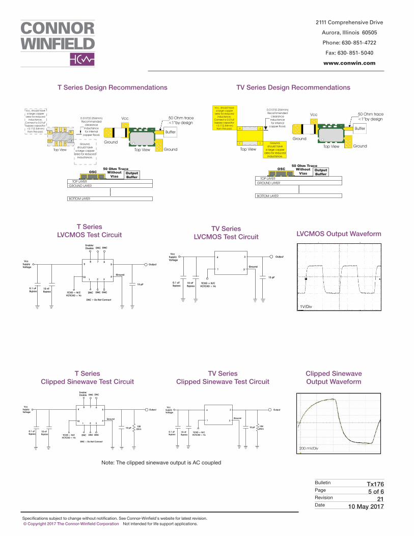
OSC
TOP LAYER
GROUND LAYER
BOTTOM LAYER
Output
Buffer
50 Ohm TraceWithout
Vias
.......
Buffer
Ground
50 Ohm trace
<1”by designVcc
Ground
Top View
0.010”(0.254mm)
Recommended
clearance
inductance
for internal
copper flood.
4
59
10
4
1 2
3
Vcc, should have
a large copper
area for reduced
inductance.
Connect a 0.01uF
bypass capacitor
<0.1”(2.54mm)
from the pad.
Ground,
should have
a large copper
area for reduced
inductance.
Top View
T Series Design Recommendations
OSC
TOP LAYER
GROUND LAYER
BOTTOM LAYER
Output
Buffer
50 Ohm TraceWithout
Vias
.......
Vcc, should have
a large copper
area for reduced
inductance.
Connect a 0.01uF
bypass capacitor
<0.1”(2.54mm)
from the pad.
Ground,
should have
a large copper
area for reduced
inductance.
0.010”(0.254mm)
Recommended
clearance
inductance
for internal
copper flood.
Top View
1 34
568
9
10
Buffer
Ground
50 Ohm trace
<1”by designVcc
Ground
Top View
TV Series Design Recommendations
T Series LVCMOS Test Circuit
TV Series LVCMOS Test Circuit
4
5
1 2 3
678
10
TCXO = N/C
VCTCXO = Vc
DNC
DNC DNC
DNC DNC
Enable/
Disable
Output
15 pF
Ground
9
Vcc
Supply
Voltage
10 nF
Bypass
0.1 uF
Bypass
DNC = Do Not Connect
1 2
34
10 nF
Bypass
0.1 uF
Bypass
Vcc
Supply
Voltage
TCXO = N/C
VCTCXO = Vc
Ground
15 pF
Output
1V/Div
LVCMOS Output Waveform
T Series Clipped Sinewave Test Circuit
TV Series Clipped Sinewave Test Circuit
4
5
1 2 3
678
10
TCXO = N/C
VCTCXO = Vc
DNC
DNC DNC
DNC DNC
Enable/
Disable
Output
Ground
9
Vcc
Supply
Voltage
10 nF
Bypass
0.1 uF
Bypass
DNC = Do Not Connect
10 pF10K
Ohm
1 2
34
10 nF
Bypass
0.1 uF
Bypass
Vcc
Supply
Voltage
TCXO = N/C
VCTCXO = Vc
Ground
10 pF
Output
10K
Ohm
200 mV/Div
0
Clipped Sinewave Output Waveform
Note: The clipped sinewave output is AC coupled
Specifications subject to change without notification. See Connor-Winfield's website for latest revision. © Copyright 2017 The Connor-Winfield Corporation Not intended for life support applications.
2111 Comprehensive Drive
Aurora, Illinois 60505
Phone: 630-851-4722
Fax: 630- 851- 5040
www.conwin.com
Bulletin Tx176Page 6 of 6Revision 21Date 10 May 2017
Revision HistoryRevision Date Action 17 02/11/14 Updated specifications and combined the T and TV series data sheets. 18 09/15/14 Added Alternate Package Outline 19 04/01/15 Updated Frequency Stabilities 20 07/27/16 Extended operating frequency range, and updated standard frequency list 21 05/10/17 Added marking variations
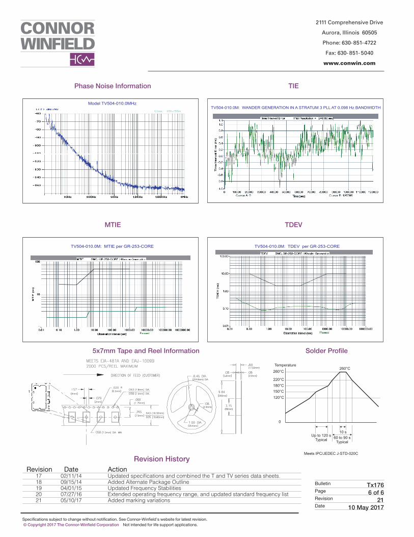
1
Solder Profile
120°C
150°C
180°C
260°C
0
220°C
Up to 120 sTypical
10 s60 to 90 s
Typical
Temperature260°C
Meets IPC/JEDEC J-STD-020C
5x7mm Tape and Reel Information
Model TV504-010.0MHz
Phase Noise Information TIE
TV504-010.0M: WANDER GENERATION IN A STRATUM 3 PLL AT 0.098 Hz BANDWIDTH
TV504-010.0M: MTIE per GR-253-CORE
MTIE TDEV
TV504-010.0M: TDEV per GR-253-CORE
![· 430 mhz fm mobile transceiver dj-520j dual band fm handy transceiver dj-530j 144/430mhz dual band fm handy transceiver . r 10f3 r 10173] (tcxo) (tcxo) digital ej-47u ¥14,800](https://img.pdfslide.net/doc/110x75/604c0c10cc37c0411e3ddecf/430-mhz-fm-mobile-transceiver-dj-520j-dual-band-fm-handy-transceiver-dj-530j-144430mhz.jpg)