Embed Size (px)
Citation preview
Real-Time Computing and Communications Lab., Hanyang Universityhttp://rtcc.hanyang.ac.kr
Real-Time Computing and Communications Lab., Hanyang Universityhttp://rtcc.hanyang.ac.kr
AVR Microcontrollers(ATMega128)
Minsoo Ryu
Department of Computer Science and EngineeringHanyang University

2Real-Time Computing and Communications Lab., Hanyang University
http://rtcc.hanyang.ac.kr 2Real-Time Computing and Communications Lab., Hanyang Universityhttp://rtcc.hanyang.ac.kr
Topics Covered
IntroductionMain Features Architectural OverviewMemory Organization

3Real-Time Computing and Communications Lab., Hanyang University
http://rtcc.hanyang.ac.kr 3Real-Time Computing and Communications Lab., Hanyang Universityhttp://rtcc.hanyang.ac.kr
Atmel AVR
The AVR is a Modified Harvard architecture 8-bit RISC single chip microcontroller (µC) which was developed by Atmel in 1996
The AVR was one of the first microcontroller families to use on-chip flash memory for program storage One-Time Programmable ROM, EPROM, or EEPROM used by
other microcontrollers at the time The AVR allows users to download a program to the board
without a ROM Writer using the ISP (In-System Programming) function

4Real-Time Computing and Communications Lab., Hanyang University
http://rtcc.hanyang.ac.kr 4Real-Time Computing and Communications Lab., Hanyang Universityhttp://rtcc.hanyang.ac.kr
History
It is believed the AVR basic architecture was conceived by two students at the Norwegian Institute of Technology (NTH) Alf-Egil Bogen and Vegard Wollan The original AVR MCU was developed at a local ASIC house
in Trondheim, Norway, where the two founders of Atmel Norway were working as students
5Real-Time Computing and Communications Lab., Hanyang University
http://rtcc.hanyang.ac.kr 5Real-Time Computing and Communications Lab., Hanyang Universityhttp://rtcc.hanyang.ac.kr
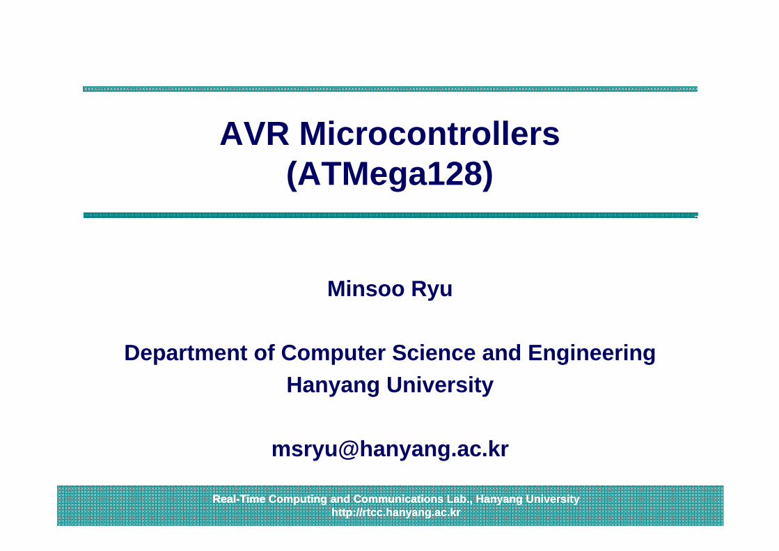
Basic Families
Family Description
tinyAVR(The ATtiny series)
- 1~8 kB program memory - 8~32-pin package - Limited peripheral set
megaAVR(The ATmega series)
- 4~256 kB program memory - 28–100-pin package - Extended instruction set (Multiply instructions and instructions for handling larger program memories) - Extensive peripheral set
XMEGA(The ATxmega series)
- 16~384 kB program memory - 44~64~100-pin package (A4, A3, A1) - Extended performance features, such as DMA, "Event System", and cryptography support- Extensive peripheral set with DACs
Application-Specific AVR- megaAVRs with special features not found on the other members of the AVR family, such as LCD controller, USB controller, advanced PWM, CAN etc

6Real-Time Computing and Communications Lab., Hanyang University
http://rtcc.hanyang.ac.kr 6Real-Time Computing and Communications Lab., Hanyang Universityhttp://rtcc.hanyang.ac.kr
Main Features of the ATMega Series (1/2)
Tuned for high level languages Simple addressing mode Every register is an accumulator
Consistent architecture across entire line Small AVR are subsets of larger chips: same hardware and
code works across all chips High performance
Most single clock cycle execution for 133 Instructions – 32 x 8 General Purpose Working Registers + Peripheral
Control Registers Up to 16 MIPS Throughput at 16 MHz
• 0 - 8 MHz ATmega128L• 0 - 16 MHz ATmega128
On-chip 2-cycle Multiplier

7Real-Time Computing and Communications Lab., Hanyang University
http://rtcc.hanyang.ac.kr 7Real-Time Computing and Communications Lab., Hanyang Universityhttp://rtcc.hanyang.ac.kr
Main Features of the ATMega Series (2/2)
JTAG support For on chip debugging
Six software selectable power saving modes The Idle mode stops the CPU while allowing the SRAM,
Timer/Counters, SPI port, and interrupt system to continue functioning
The Power-down mode saves the register contents but freezes the Oscillator, disabling all other chip functions until the next interrupt or Hardware Reset
Others include Power-save mode, ADC Noise Reduction mode, Standby mode, and Extended Standby mode

8Real-Time Computing and Communications Lab., Hanyang University
http://rtcc.hanyang.ac.kr 8Real-Time Computing and Communications Lab., Hanyang Universityhttp://rtcc.hanyang.ac.kr
Pin Configurations

9Real-Time Computing and Communications Lab., Hanyang University
http://rtcc.hanyang.ac.kr 9Real-Time Computing and Communications Lab., Hanyang Universityhttp://rtcc.hanyang.ac.kr
Block Diagram

10Real-Time Computing and Communications Lab., Hanyang University
http://rtcc.hanyang.ac.kr 10Real-Time Computing and Communications Lab., Hanyang Universityhttp://rtcc.hanyang.ac.kr
CPU Core

11Real-Time Computing and Communications Lab., Hanyang University
http://rtcc.hanyang.ac.kr 11Real-Time Computing and Communications Lab., Hanyang Universityhttp://rtcc.hanyang.ac.kr
Architectural Overview
Single level pipelining While one instruction is being executed, the next instruction
is pre-fetched from the program memory This concept enables instructions to be executed in every
clock cycle
The fast-access Register file contains 32 x 8-bit general purpose working registers with a single clock cycle access time This allows single-cycle Arithmetic Logic Unit (ALU)
operation In a typical ALU operation, two operands are output from the
Register file, the operation is executed, and the result is stored back in the Register file – in one clock cycle

12Real-Time Computing and Communications Lab., Hanyang University
http://rtcc.hanyang.ac.kr 12Real-Time Computing and Communications Lab., Hanyang Universityhttp://rtcc.hanyang.ac.kr
Architectural Overview
High-performance ALU The ALU operates in direct connection with all the 32 general
purpose working registers Within a single clock cycle, arithmetic operations between
general purpose registers or between a register and an immediate are executed
The ALU operations are divided into three main categories –arithmetic, logical, and bit-functions
Some implementations of the architecture also provide a powerful multiplier supporting both signed/unsigned multiplication and fractional format

13Real-Time Computing and Communications Lab., Hanyang University
http://rtcc.hanyang.ac.kr 13Real-Time Computing and Communications Lab., Hanyang Universityhttp://rtcc.hanyang.ac.kr
Status Register (SREG)
I (Global Interrupt Enable) The I-bit is cleared by hardware after an interrupt has occurred,
and is set by the RETI instruction to enable subsequent interrupts
The I-bit can also be set and cleared in software with the SEI and CLI instructions, as described in the instruction set reference
T (Bit Copy Storage) The Bit Copy instructions BLD (Bit LoaD) and BST (Bit STore)
use the T-bit as source or destination for the operated bit A bit from a register in the Register file can be copied into T by
the BST instruction, and a bit in T can be copied into a bit in a register in the Register file by the BLD instruction

14Real-Time Computing and Communications Lab., Hanyang University
http://rtcc.hanyang.ac.kr 14Real-Time Computing and Communications Lab., Hanyang Universityhttp://rtcc.hanyang.ac.kr
Status Register (SREG)
H (Half Carry Flag) Holds the carry from bit 3 to bit 4 To support operations on four bits
S (Sign Bit) Is always an exclusive or between the negative flag N and the
two’s complement overflow flag V V (Overflow Flag)
Supports two’s complement arithmetic N (Negative Flag)
Indicates a negative result in an arithmetic or logic operation Z (Zero Flag)
Indicates a zero result in an arithmetic or logic operation C (Carry Flag)
Indicates a carry in an arithmetic or logic operation

15Real-Time Computing and Communications Lab., Hanyang University
http://rtcc.hanyang.ac.kr 15Real-Time Computing and Communications Lab., Hanyang Universityhttp://rtcc.hanyang.ac.kr
32 General Purpose Registers
Each register is also assigned a data memory address, mapping them directly into the first 32 locations of the user Data Space

16Real-Time Computing and Communications Lab., Hanyang University
http://rtcc.hanyang.ac.kr 16Real-Time Computing and Communications Lab., Hanyang Universityhttp://rtcc.hanyang.ac.kr
The X-, Y-, and Z-registers
The registers R26 ~ R31 have some added functions to their general purpose usage These registers are 16-bit address pointers for indirect
addressing of the Data Space

17Real-Time Computing and Communications Lab., Hanyang University
http://rtcc.hanyang.ac.kr 17Real-Time Computing and Communications Lab., Hanyang Universityhttp://rtcc.hanyang.ac.kr
Stack Pointer
The Stack is mainly used for storing temporary data, for storing local variables and for storing return addresses after interrupts and subroutine calls
The Stack Pointer Register always points to the top of the Stack Note that the Stack is implemented as growing from higher
memory locations to lower memory locations This implies that a Stack PUSH command decreases the
Stack Pointer The AVR Stack Pointer is implemented as two 8-bit registers
in the I/O space

18Real-Time Computing and Communications Lab., Hanyang University
http://rtcc.hanyang.ac.kr 18Real-Time Computing and Communications Lab., Hanyang Universityhttp://rtcc.hanyang.ac.kr
Flash Program Memory
The AVR architecture has two main memory spaces, the Data Memory and the Program Memory space Flash Program memory SRAM Data Memory
The ATmega128 contains 128K bytes On-chip In-System Reprogrammable Flash memory for program storage The Flash memory has an endurance of at least 10,000
write/erase cycles Since all AVR instructions are 16 or 32 bits wide, the Flash is
organized as 64K x 16 The ATmega128 Program Counter (PC) is 16 bits wide, thus
addressing the 64K program memory locations For software security, the Flash Program memory space is
divided into two sections, Boot Program section and Application Program section

19Real-Time Computing and Communications Lab., Hanyang University
http://rtcc.hanyang.ac.kr 19Real-Time Computing and Communications Lab., Hanyang Universityhttp://rtcc.hanyang.ac.kr
Program Memory Map

20Real-Time Computing and Communications Lab., Hanyang University
http://rtcc.hanyang.ac.kr 20Real-Time Computing and Communications Lab., Hanyang Universityhttp://rtcc.hanyang.ac.kr
SRAM Data Memory
Two configurations
Register file from 0x0000 I/O Registers Extended I/O Registers Internal SRAM External SRAM

21Real-Time Computing and Communications Lab., Hanyang University
http://rtcc.hanyang.ac.kr 21Real-Time Computing and Communications Lab., Hanyang Universityhttp://rtcc.hanyang.ac.kr
SRAM Data Memory

22Real-Time Computing and Communications Lab., Hanyang University
http://rtcc.hanyang.ac.kr 22Real-Time Computing and Communications Lab., Hanyang Universityhttp://rtcc.hanyang.ac.kr
I/O Register Access
All I/O locations may be accessed by the LD/LDS/LDD and ST/STS/STD instructions, transferring data between the 32 general purpose working registers and the I/O space
They can also be accessed by the IN and OUT instructions and the I/O addresses $00 - $3F must be used When addressing I/O registers as data space using LD and
ST instructions, $20 must be added to these addresses I/O registers within the address range $00 - $1F are directly
bit-accessible using the SBI and CBI instructions

23Real-Time Computing and Communications Lab., Hanyang University
http://rtcc.hanyang.ac.kr 23Real-Time Computing and Communications Lab., Hanyang Universityhttp://rtcc.hanyang.ac.kr
External SRAM Access
When the addresses accessing the SRAM memory space exceeds the internal data memory locations, the external data SRAM is accessed using the same instructions as for the internal data memory access
Accessing external SRAM takes one additional clock cycle per byte compared to access of the internal SRAM This means that the commands LD, ST, LDS, STS, LDD, STD,
PUSH, and POP take one additional clock cycle If the Stack is placed in external SRAM, interrupts, subroutine
calls and returns take three clock cycles extra because the two-byte program counter is pushed and popped, and external memory access does not take advantage of the internal pipe-line memory access
24Real-Time Computing and Communications Lab., Hanyang University
http://rtcc.hanyang.ac.kr 24Real-Time Computing and Communications Lab., Hanyang Universityhttp://rtcc.hanyang.ac.kr
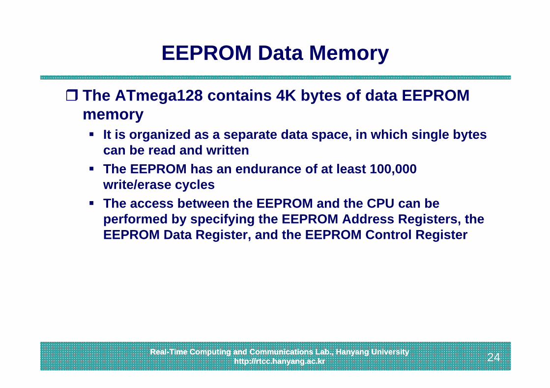
EEPROM Data Memory
The ATmega128 contains 4K bytes of data EEPROM memory It is organized as a separate data space, in which single bytes
can be read and written The EEPROM has an endurance of at least 100,000
write/erase cycles The access between the EEPROM and the CPU can be
performed by specifying the EEPROM Address Registers, the EEPROM Data Register, and the EEPROM Control Register

25Real-Time Computing and Communications Lab., Hanyang University
http://rtcc.hanyang.ac.kr 25Real-Time Computing and Communications Lab., Hanyang Universityhttp://rtcc.hanyang.ac.kr
Instruction Set

26Real-Time Computing and Communications Lab., Hanyang University
http://rtcc.hanyang.ac.kr 26Real-Time Computing and Communications Lab., Hanyang Universityhttp://rtcc.hanyang.ac.kr
Instruction Set

27Real-Time Computing and Communications Lab., Hanyang University
http://rtcc.hanyang.ac.kr 27Real-Time Computing and Communications Lab., Hanyang Universityhttp://rtcc.hanyang.ac.kr
Instruction Set

28Real-Time Computing and Communications Lab., Hanyang University
http://rtcc.hanyang.ac.kr 28Real-Time Computing and Communications Lab., Hanyang Universityhttp://rtcc.hanyang.ac.kr
Instruction Set

29Real-Time Computing and Communications Lab., Hanyang University
http://rtcc.hanyang.ac.kr 29Real-Time Computing and Communications Lab., Hanyang Universityhttp://rtcc.hanyang.ac.kr
Instruction Set


![[PPT]PowerPoint Presentation - 조원경교수 강의 홈페이지chowk.khu.ac.kr/lecture/AVR/lecture_note_ppt/avr_uart.pptx · Web viewKyungHee Univ. 2-ATmega128 USART USART : UART](https://img.pdfslide.net/doc/110x75/5b2ab3637f8b9a55068b750b/pptpowerpoint-presentation-chowkkhuackrlectureavrlecturenotepptavruartpptx.jpg)