Embed Size (px)
Citation preview

AVR- PX128A1 development board Users Manual
All boards produced by Olimex are ROHS compliant
Rev.B, May 2009Copyright(c) 2009, OLIMEX Ltd, All rights reserved
Page 1

INTRODUCTION
AVR-PX128A1 board is entry level development board for the new AVR XMEGATM
A Microcontroller family of devices produced by Atmel Corporation.
With AVR-PX128A1 you can explore the features of XMEGA A family on budged, the board have everything necessary to build simple applications: USB port where power is taken and power supply circuit, reset and oscillator circuits, JTAG and PDI port for programming and debugging, LCD, status LED and two user buttons.
Although very simple this board will allow you to easily build USB application like USB mass storage device, USB Audio class device, USB to Virtual RS232 port. There are plenty of GPIOs on extension headers where you can connect your additional circuits.
BOARD FEATURES- CPU: ATXMEGA128A1 AVR 8/16-bit XMEGATM
- JTAG connector with standard 2x5 pin layout for programming/debugging with JTAGICE mkII
- PDI connector with 2x3 pin layout for programming/debugging with JTAGICE mkII
- USB connector
- two user buttons
- RESET button
- status LED
- power supply LED
- on board voltage regulator 3.3V with up to 800mA current
- single power supply: 6V AC or 9V DC required, board can take power from USB port too
- 8 Mhz crystal oscillator
- 32768 Hz crystal and RTC
- extension header
- SD/MMC card connector
- Audio in and Audio Out jacks for microphone and headphones
- LCD 8X1
- PCB: FR-4, 1.5 mm (0,062"), red soldermask, silkscreen component print
- Dimensions: 100 x 80mm (3.9 x 3.15")
ELECTROSTATIC WARNING
The AVR-PX128A1 board is shipped in protective anti-static packaging. The board must not be subject to high electrostatic potentials. General practice for working with static sensitive devices should be applied when working with this board.
Page 2

BOARD USE REQUIREMENTS
Cables: The cable you will need depends on the programmer/debugger you use, also you will need USB A-B cable.
Hardware: Programmer/Debugger JTAGICE mkII
Software: AVR C compiler.
PROCESSOR FEATURES
AVR-PX128A1 board use High-performance, Low-power 8/16-bit AVR XMEGA Microcontroller ATXMEGA128A1 from Atmel Corporation with these features:
– Non-Volatile Program and Data Memories:
– 128K Bytes of In-System Self-Programmable Flash
– 8K Bytes Boot Section with Independent Lock Bits
– 2K Bytes EEPROM.
– 8K Bytes Internal SRAM.
External Bus Interface for up to 16M bytes SRAM
External Bus Interface for up to 128M bit SDRAM
– Peripheral Features:
– Four-channel DMA Controller with support for external requests
– Eight-channel Event System
– Eight 16-bit Timer/Counters
Four Timer/Counters with 4 Output Compare or Input Capture channels
Four Timer/Counters with 2 Output Compare or Input Capture channels
High-Resolution Extension on all Timer/Counters
Advanced Waveform Extension on two Timer/Counters
– Eight USARTs
IrDA modulation/demodulation for one USART
– Four Two-Wire Interfaces with dual address match (I2C and SMBus compatible)
– Four SPI (Serial Peripheral Interface) peripherals
– AES and DES Crypto Engine
– 16-bit Real Time Counter with separate Oscillator
– Two Eight-channel, 12-bit, 2 Msps Analog to Digital Converters
– Two Two-channel, 12-bit, 1 Msps Digital to Analog Converters
– Four Analog Comparators with Window compare function
Page 3

– External Interrupts on all General Purpose I/O pins
– Programmable Watchdog Timer with Separate On-chip Ultra Low Power Oscillator
– Special Microcontroller Features
– Power-on Reset and Programmable Brown-out Detection
– Internal and External Clock Options with PLL and Prescaler
– Programmable Multi-level Interrupt Controller
– Sleep Modes: Idle, Power-down, Standby, Power-save, Extended Standby
– Advanced Programming, Test and Debugging Interfaces
JTAG (IEEE 1149.1 Compliant) Interface for programming, test and debugging
PDI (Program and Debug Interface) for programming and debugging
– I/O
– 78 Programmable I/O Lines
– Operating Voltage
– 1.6 – 3.6V
– Speed performance
– 0 – 12 MHz @ 1.6 – 3.6V
– 0 – 32 MHz @ 2.7 – 3.6V
Page 4

BLOCK DIAGRAM
MEMORY MAP
Page 5

Page 6
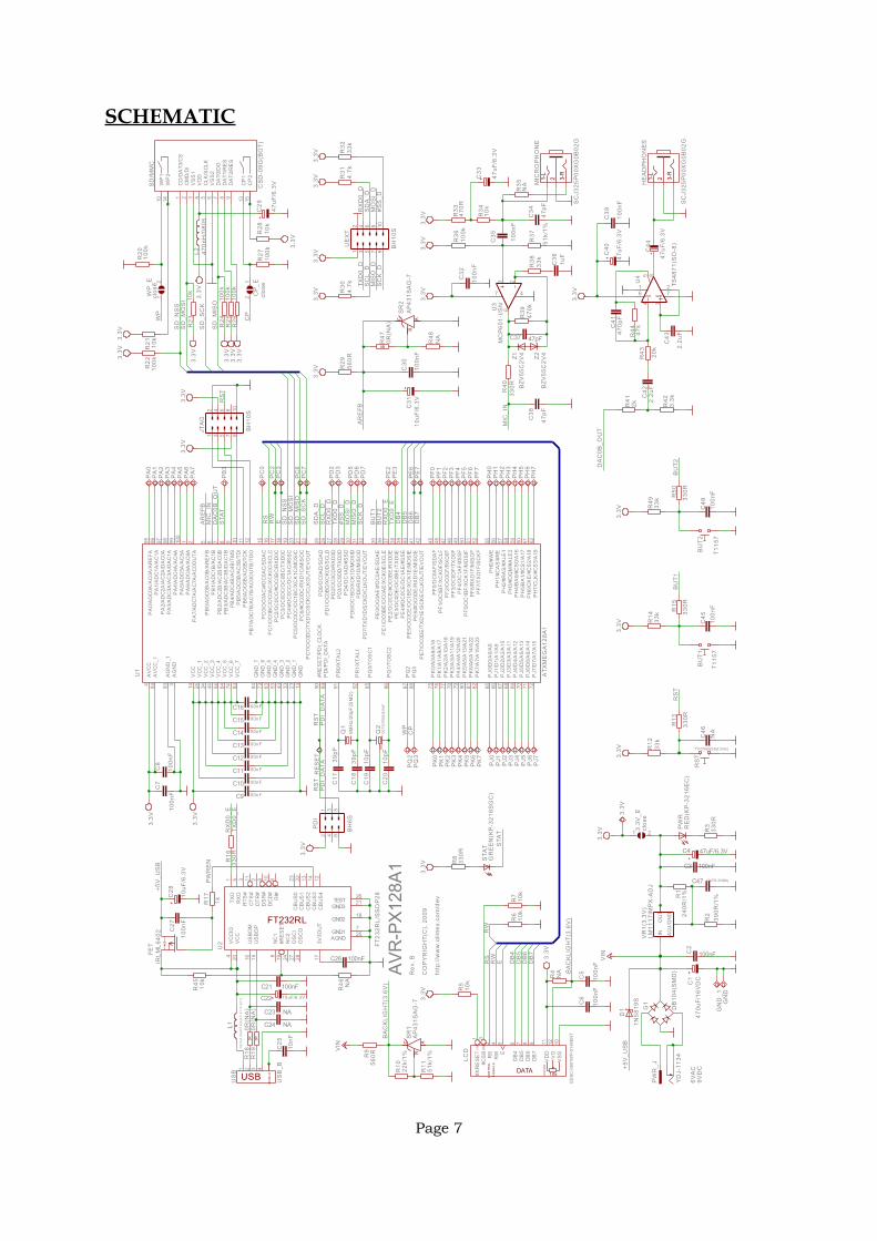
SCHEMATIC
Page 7
clos
e
T115
7T1
157
470u
F/16
VD
C
100nF
100nF
47uF/6.3V
100n
F10
0nF
100n
F10
0nF
100nF
100nF
100nF
100nF
100nF
100nF
100nF
100nF
39pF
39pF
10pF
10pF
100nF10uF/6.3V
NA
NA
10nF
100nF
100n
F10
uF/6
.3V
47uF
/6.3
V
100n
F10
uF/6
.3V
100n
F
47uF
/6.3
V
47pF
100n
F
1uF
47pF
47pF
100n
F47
uF/6
.3V
470p
F
2.2u
F
2.2u
F
47uF
/6.3
V
100n
FN
A
10uF/6.3V(NA)
100n
F
clos
e
1N58
19S
IRLM
L640
2
DB
104(
SM
D)
BH
10S
FB
/60
0 O
HM
/12
06(3
216
11
C-6
01
)
470n
H/0
805
GD
SC-0
801W
P-01
-MEN
T
VIN
VIN
BH
6S
RE
D(K
P-3
216E
C)
YD
J-11
34
8MH
z/20
pF(S
MD
)
QC
T327
68(2
x6)/6
pF
240R
/1%
390R
/1%
330R
NA
10k
10k
10k
330R
560R
22k/
1%
51k/
1%
33k
330R
33k 33
0R
330R
1k
0R(N
A)
0R(N
A)
100k
10k
100k
10k
100k
100k
100k
100k
10k
560R
4.7k
4.7k
33k
470R
10k
NA
100k
51k/
1%33
k47
0k
330R
2k 3.3k
20k
47k
10k
NA
0R(N
A)
NA
33k 33
0R
T1107A(6x3.8x2.5mm)
CS
D-0
9G(B
OT)
AP
431S
AG
-7A
P43
1SA
G-7
GR
EE
N(K
P-3
216S
GC
)
ATX
ME
GA
128A
1
FT23
2RL/
SS
OP
28
MC
P60
1-I/S
N
TS48
71(S
O-8
)BH
10S
US
B_B
3.3V
3.3V
3.3V
3.3V
3.3V
3.3V
3.3V
3.3V
3.3V
3.3V
3.3V
3.3V
3.3V
3.3V
3.3V
3.3V
3.3V
3.3V
3.3V
3.3V
3.3V
3.3V
3.3V
3.3V
3.3V
3.3V
3.3V
3.3V
3.3V
LM11
17IM
PX
-AD
J
clos
e
BZV
55C
2V4
BZV
55C
2V4
#SS
_D
#SS
_D
+5V
_US
B
+5V
_US
B
AR
EFB
AR
EFB
BA
CK
LIG
HT(
3.6V
)
BA
CK
LIG
HT(
3.6V
)
BU
T1
BU
T1
BU
T2
BU
T2
CP
CP
DA
C0B
_OU
T
DA
C0B
_OU
T
DB
4
DB
4
DB
5
DB
5
DB
6
DB
6
DB
7
DB
7
E
E
MIC
_IN
MIC
_IN
MIS
O_D
MIS
O_D
MO
SI_
D
MO
SI_
D
PD
I_D
ATA
PD
I_D
ATA
PW
RE
N
RS
RS
RS
T
RS
TR
ST
RS
T
RW
RW
RW
RX
D0_
D
RX
D0_
D
RX
D0_
E
RX
D0_
E
SC
K_D
SC
K_D
SC
L_D
SC
L_D
SD
A_D
SD
A_D
SD
_MIS
O
SD
_MIS
O
SD
_MO
SI
SD
_MO
SI
SD
_NS
S
SD
_NS
S
SD
_SC
K
SD
_SC
K
STA
T
STA
T
TXD
0_D
TXD
0_D
TXD
0_E
TXD
0_E
WP
WP
3.3V
1 2
3.3V
_E
BU
T1B
UT2
C1
C2
C3
C4
C5
C6
C7
C8
C9
C10
C11
C12
C13
C14
C15
C16
C17
C18
C19
C20
C21
C22
C23
C24
C25
C26
C27
C28
C29
C30
C31
C32
C33
C34
C35
C36
C37
C38
C39
C40
C41
C42
C43
C44
C45
C46
C47
C48
12 C
P_E
D1
FET
G1 G
ND
GN
D_1
HE
AD
PH
ON
ES
SC
J325
P00
XG
0B02
G
12
34
56
78
910
JTA
G
L1
L2
#CS
B3
#XR
ES
ET
1
DB
46
DB
57
DB
68
DB
79
E5
RS
2
RW
4
VD
D11
VO
12
VS
S10
LCD
MIC
RO
PH
ON
E
SC
J325
P00
XG
0B02
G
PA
0P
A1
PA
2P
A3
PA
4P
A5
PA
6P
A7
PB
3
PC
0P
C2
PC
3
PC
6P
C7
PD
2P
D3
PD
5P
D6
PD
7
12
34
56
PD
I
PE
2P
E3
PE
6P
E7
PF0
PF1
PF2
PF3
PF4
PF5
PF6
PF7
PH
0P
H1
PH
2P
H3
PH
4P
H5
PH
6P
H7
PJ0
PJ1
PJ2
PJ3
PJ4
PJ5
PJ6
PJ7
PK
0P
K1
PK
2P
K3
PK
4P
K5
PK
6P
K7
PQ
2P
Q3
PW
R
PW
R_J
Q1
Q2
R1
R2
R3
R4
R5
R6
R7
R8
R9
R10
R11
R12
R13
R14
R15
R16
R17
R18
R19
R20
R21
R22
R23
R24
R25
R26
R27
R28
R29
R30
R31
R32
R33
R34
R35
R36
R37
R38
R39
R40
R41
R42
R43
R44
R45
R46
R47
R48
R49
R50
RE
SE
T
RS
T
CD
/DA
T3/C
S1
CLK
/SC
LK5
CM
D/D
I2
CP
113
CP
215
DA
T0/D
O7
DA
T1/R
ES
8
DA
T2/R
ES
9
VD
D4
VS
S1
3
VS
S2
6
WP
110
WP
214
SD
/MM
C
SR
1S
R2
STA
T
#RE
SE
T/P
DI_
CLO
CK
90
AG
ND
3A
GN
D_1
93
AV
CC
4
AV
CC
_194
GN
D13
GN
D_1
23G
ND
_233
GN
D_3
43G
ND
_453
GN
D_5
63G
ND
_673
GN
D_7
84
PA
0/A
DC
0A/A
C0A
/AR
EFA
95
PA
1/A
DC
1A/A
C1A
96
PA
2/A
DC
2A/A
C2A
/DA
C0A
97
PA
3/A
DC
3A/A
C3A
/DA
C1A
98
PA
4/A
DC
4A/A
C4A
99
PA
5/A
DC
5A/A
C5A
100
PA
6/A
DC
6A/A
C6A
1
PA
7/A
DC
7A/A
C7A
/AC
0OU
TA2
PB
0/A
DC
0B/A
C0B
/AR
EFB
5
PB
1/A
DC
1B/A
C1B
6
PB
2/A
DC
2B/A
C2B
/DA
C0B
7
PB
3/A
DC
3B/A
C3B
/DA
C1B
8
PB
4/A
DC
4B/A
C4B
/TM
S9
PB
5/A
DC
5B/A
C5B
/TD
I10
PB
6/A
DC
6B/A
C6B
/TC
K11
PB
7/A
DC
7B/A
C7B
/AC
0OU
TB/T
DO
12
PC
0/O
C0A
C/#
OC
0AC
/SD
AC
15
PC
1/O
C0B
C/O
C0A
C/X
CK
0C/S
CLC
16
PC
2/O
C0C
C/#
OC
0BC
/RX
D0C
17
PC
3/O
C0D
C/O
C0B
C/T
XD
0C18
PC
4/#O
C0C
C/O
C1A
C/#
SS
C19
PC
5/O
C0C
C/O
C1B
C/X
CK
1C/M
OS
IC20
PC
6/#O
C0D
C/R
XD
1C/M
ISO
C21
PC
7/O
C0D
C/T
XD
1C/S
CK
C/C
LKO
UT/
EV
OU
T22
PD
0/O
C0A
D/S
DA
D25
PD
1/O
C0B
D/X
CK
0D/S
CLD
26
PD
2/O
C0C
D/R
XD
0D27
PD
3/O
C0D
D/T
XD
0D28
PD
4/O
C1A
D/#
SS
D29
PD
5/O
C1B
D/X
CK
1D/M
OS
ID30
PD
6/R
XD
1D/M
ISO
D31
PD
7/TX
D1D
/SC
KD
/CLK
OU
T/E
VO
UT
32
PD
I/PD
I_D
ATA
89
PE
0/O
C0A
E/#
OC
0AE
/SD
AE
35
PE
1/O
C0B
E/O
C0A
E/X
CK
0E/S
CLE
36
PE
2/O
C0C
E/#
OC
0BE
/RX
D0E
37
PE
3/O
C0D
E/O
C0B
E/T
XD
0E38
PE
4/#O
C0C
E/O
C1A
E/#
SS
E39
PE
5/O
C0C
E/O
C1B
E/X
CK
1E/M
OS
IE40
PE
6/#O
C0D
E/R
XD
1E/M
ISO
E41
PE
7/O
C0D
E/T
XD
1E/S
CK
E/C
LKO
UT/
EV
OU
T42
PF0
/OC
0AF/
SD
AF
45
PF1
/OC
0BF/
XC
K0F
/SC
LF46
PF2
/OC
0CF/
RX
D0F
47
PF3
/OC
0DF/
TXD
0F48
PF4
/OC
1AF/
#SS
F49
PF5
/OC
1BF/
XC
K1F
/MO
SIF
50
PF6
/RX
D1F
/MIS
OF
51
PF7
/TX
D1F
/SC
KF
52
PH
0/#W
E55
PH
1/#C
AS
/#R
E56
PH
2/#R
AS
/#A
LE1
57
PH
3/#D
QM
/#A
LE2
58
PH
4/B
A0/
#CS
0/A
1659
PH
5/B
A1/
#CS
1/A
1760
PH
6/C
KE
/#C
S2/
A18
61
PH
7/C
LK/#
CS
3/A
1962
PJ0
/D0/
A0/
A8
65
PJ1
/D1/
A1/
A9
66
PJ2
/D2/
A2/
A10
67
PJ3
/D3/
A3/
A11
68
PJ4
/D4/
A4/
A12
69
PJ5
/D5/
A5/
A13
70
PJ6
/D6/
A6/
A14
71
PJ7
/D7/
A7/
A15
72
PK
0/A
0/A
8/A
1675
PK
1/A
1/A
9/A
1776
PK
2/A
2/A
10/A
1877
PK
3/A
3/A
11/A
1978
PK
4/A
4/A
12/A
2079
PK
5/A
5/A
13/A
2180
PK
6/A
6/A
14/A
2281
PK
7/A
7/A
15/A
2382
PQ
0/TO
SC
185
PQ
1/TO
SC
286
PQ
287
PQ
388
PR
0/X
TAL2
91
PR
1/X
TAL1
92
VC
C14
VC
C_1
24
VC
C_2
34
VC
C_3
44
VC
C_4
54
VC
C_5
64
VC
C_6
74
VC
C_7
83
U1
#RE
SE
T19
3V3O
UT
17
AGND25
CB
US
023
CB
US
122
CB
US
213
CB
US
314
CB
US
412
CTS
#11
DC
D#
10D
SR
#9
DTR
#2
GND17
GND218
GND321
NC
18
NC
224
OS
CI
27
OS
CO
28
RI#
6
RTS
#3
RX
D5
TEST26
TXD
1
US
BD
M16
US
BD
P15
VC
C20
VC
CIO
4U
2
3 26
7 4
U3 34
27
5 8
16
U4
12
34
56
78
910
UE
XT
1 2 3 4
US
B
AD
J/G
ND
INO
UT
VR
1(3.
3V)
12
WP
_E
Z1 Z2
6VA
C9V
DC
AVR
-PX1
28A1
Rev
. B
CO
PY
RIG
HT(
C),
200
9
http
://w
ww
.olim
ex.c
om/d
ev
+
+
+
+
+
+
+
+
+1-
L2 3-
R
10kCON
TRA
ST
DATA
CO
NT
RO
L
SIG
NA
LS
(1)
(0)
1-L
2 3-R
GND
0R 0R
0R
C AR
C AR
FT232RL
VCC GND
USB
SH
IEL
D

BOARD LAYOUT
Page 8

POWER SUPPLY CIRCUITAVR-PX128A1 is typically power supplied with 9 V DC, and 6 V AC.
The board power consumption is about 30mA.
RESET CIRCUITAVR-PX128A1 reset circuit includes pin 5 of PDI connector, pin 6 of JTAG connector, ATXMEGA128A1 pin 90 and Reset button.
CLOCK CIRCUITQuartz crystal 8MHz is connected to ATXMEGA128A1 pin 91 (PR0/XTAL2) and pin 92 (PR1/XTAL1).
Page 9

JUMPER DESCRIPTION3.3V_E
Enable the main 3.3 V regulator VR1(3.3V) – LM1117.
Default state is closed.WP_E
Enable SD/MMC Write Protect signal check.Default state is closed.
CP_EEnable SD/MMC Card Present signal check.Default state is closed.
INPUT/OUTPUTStatus LED (green) with name STAT connected to ATXMEGA128A1 pin 8 (PB3/ADC3B/AC3B/DAC1B) and EXT pin PB3.
Power-on LED (red) with name PWR – this led shows that +3.3V is applied to the board.
User button with name BUT1 connected to ATXMEGA128A1 pin 35 (PE0/OC0AE/#OC0AE/SDAE).
User button with name BUT2 connected to ATXMEGA128A1 pin 36 (PE1/OC0BE/#XCK0E/SCLE).
Reset button with name RST connected to pin 5 of PDI connector, pin 6 of JTAG connector, ATXMEGA128A1 pin 90 (#RESET/PDI_CLOCK).
CONNECTOR DESCRIPTIONS
JTAG
Pin # Signal Name
1 PB6
2 GND
3 PB7
4 3.3V
5 PB4
6 RST
7 3.3V
8 NC
9 PB5
10 GND
Page 10

PDI
Pin # Signal Name
1 PDI_DATA
2 3.3V
3 NC
4 NC
5 RST
6 GND
UEXT
Pin # Signal Name
1 3.3V
2 GND
3 TXD0_D
4 RXD0_D
5 SCL_D
6 SDA_D
7 MISO_D
8 MOSI_D
9 SCK_D
10 #SS_D
USBPin # Signal Name
1 +5V_USB
2 USBDM
3 USBDP
4 GND
Page 11

EXT
Pin # Signal Name Pin # Signal Name
1 VCC 2 VCC
3 PA7 4 PK7
5 PA6 6 PK6
7 PA5 8 PK5
9 PA4 10 PK4
11 PA3 12 PK3
13 PA2 14 PK2
15 PA1 16 PK1
17 PA0 18 PK0
19 PB3 (STAT) 20 PJ7
21 PC7 (SD_SCK) 22 PJ6
23 PC6 (SD_MISO) 24 PJ5
25 PC3 (E) 26 PJ4
27 PC2 (RW) 28 PJ3
29 PC0 30 PJ2
31 PD7 (SCK_D) 32 PJ1
33 PD6 (MISO_D) 34 PJ0
35 PD5 (MOSI_D) 36 PH7
37 PD3 (TXD0_D) 38 PH6
39 PD2 (RXD0_D) 40 PH5
41 PE7 (DB7) 42 PH4
43 PE6 (DB6) 44 PH3
45 PE3 (TXD0_E) 46 PH2
47 PE2 (RXD0_E) 48 PH1
49 PF7 50 PH0
51 PF6 52 PQ3 (CP)
53 PF5 54 PQ2 (WP)
55 PF4 56 PF0
57 PF3 58 PF1
59 RST 60 PF2
61 GND 62 GND
Page 12

PWR_JACK
Pin # Signal Name
1 Power Input
2 GND
MICROPHONE
Pin # Signal Name
1 AGND
2 NC
3 MIC
HEADPHONE
Pin # Signal Name
1 AGND
2 IN1=IN2
3 IN2=IN1
Page 13

SD/MMC
Pin # Signal Name Pin # Signal Name
1 SD_NSS 2 SD_MOSI
3 GND 4 3.3V
5 SD_SCK 6 GND
7 SD_MISO 8 Via 100k to 3.3V
9 Via 100k to 3.3V 10 WP
11 NC 12 NC
13 CP 14 Via 10k to 3.3V
15 Via 10k to 3.3V
MECHANICAL DIMENSIONS
Page 14

All measures are in inches.
Page 15

AVAILABLE DEMO SOFTWARE
– Accessing the XMEGA EEPROM
– Getting Started With the XMEGA Event System
– Use and configuration of IR communication module
– Using the XMEGA ADC
– Using the XMEGA Analog Comparator
– Using the XMEGA Clock System
– Using the XMEGA DAC
– Using the XMEGA DMA Controller
– Using the XMEGA External Bus Interface
– Using the XMEGA IO Pins and External Interrupts
– Using the XMEGA Real Time Counter
– Using the XMEGA Timer_Counter
– Using the XMEGA Timer_Counter Extensions
– Using the XMEGA USART
– XMEGA Interrupts and the Programmable Multi-level Interrupt Controller
Page 16

ORDER CODEAVR-PX128A1 – assembled and tested
How to order? You can order to us directly or by any of our distributors. Check our web www.olimex.com/dev for more info.
Revision history:
REV.B - create May 2009
Page 17

Disclaimer:
© 2009 Olimex Ltd. All rights reserved. Olimex®, logo and combinations thereof, are registered trademarks of Olimex Ltd. Other terms and product names may be trademarks of others.
The information in this document is provided in connection with Olimex products. No license, express or implied or otherwise, to any intellectual property right is granted by this document or in connection with the sale of Olimex products.
Neither the whole nor any part of the information contained in or the product described in this document may be adapted or reproduced in any material from except with the prior written permission of the copyright holder.
The product described in this document is subject to continuous development and improvements. All particulars of the product and its use contained in this document are given by OLIMEX in good faith. However all warranties implied or expressed including but not limited to implied warranties of merchantability or fitness for purpose are excluded.
This document is intended only to assist the reader in the use of the product. OLIMEX Ltd. shall not be liable for any loss or damage arising from the use of any information in this document or any error or omission in such information or any incorrect use of the product.
Page 18

![Hydraulic - Bondioli & Pavesi · 2018-11-19 · PA0 PA1 PA2 3PA PA3 PA4 0 10 20 30 40 50 60 70 80 90 [cm3/rev]MA1 MA2 3MA MA3 MA4 0 10 20 30 40 50 60 70 80 90 [cm3/rev]from 0,19 cm3/rev](https://img.pdfslide.net/doc/110x75/5e9ebc19d9d7940004130272/hydraulic-bondioli-pavesi-2018-11-19-pa0-pa1-pa2-3pa-pa3-pa4-0-10-20-30.jpg)