Embed Size (px)
Citation preview

DATA SHEETwww.onsemi.com
© Semiconductor Components Industries, LLC, 2015
August, 2021 − Rev. 31 Publication Order Number:
AX5043/D
Advanced High PerformanceASK and FSK Narrow-bandTransceiver for 27-1050 MHz Range
AX5043
OVERVIEW
FeaturesAdvanced Multi−channel Narrow−band Single Chip
UHF Transceiver (FSK/MSK/4−FSK/GFSK/GMSK/ASK/AFSK/FM/PSK)
Low−Power• RX
9.5 mA @ 868 MHz and 433 MHz6.5 mA @ 169 Hz
• TX at 868 Mhz7.5 mA @ 0 dBm16 mA @ 10 dBm48 mA @ 16 dBm
• 50 nA Deep Sleep Current
• 500 nA Power−down Current with Low FrequencyDuty Cycle Clock Running
Extended Supply Voltage Range• 1.8 V − 3.6 V Single Supply
High Sensitivity / High Selectivity Receiver• Data Rates from 0.1 kbps to 125 kbps
• Optional Forward Error Correction (FEC)
• Sensitivity without FEC−135 dBm @ 0.1 kbps, 868 MHz, FSK−126 dBm @ 1 kbps, 868 MHz, FSK−117 dBm @ 10 kbps, 868 MHz, FSK−107 dBm @ 100 kbps, 868 MHz, FSK−105 dBm @ 125 kbps, 868 MHz, FSK
−138 dBm @ 0.1 kbps, 868 MHz, PSK−130 dBm @ 1 kbps, 868 MHz, PSK−120 dBm @ 10 kbps, 868 MHz, PSK−109 dBm @ 100 kbps, 868 MHz, PSK−108 dBm @ 125 kbps, 868 MHz, PSK
• Sensitivity with FEC−137 dBm @ 0.1 kbps, 868 MHz, FSK−122 dBm @ 5 kbps, 868 MHz, FSK−111 dBm @ 50 kbps, 868 MHz, FSK
• High Selectivity Receiver with up to 47 dB AdjacentChannel Rejection
• 0 dBm Maximum Input Power
• > ±10% Data−rate Error Tolerance
• Support for Antenna Diversity with External AntennaSwitch
• Short Preamble Modes allow the Receiver to work withas little as 16 Preamble Bits
• Fast State Switching Times200 �s TX → RX Switching Time62 �s RX → TX Switching Time
Transmitter• Data−rates from 0.1 kbps to 125 kbps
• High Efficiency, High Linearity Integrated PowerAmplifier
• Maximum Output Power16 dBm @ 868 MHz16 dBm @ 433 MHz16 dBm @ 169 MHz
• Power Level programmable in 0.5 dB Steps
• GFSK Shaping with BT = 0.3 or BT = 0.5
• Unrestricted Power Ramp Shaping
Frequency Generation• Configurable for Usage in 27 MHz −1050 MHz Bands
• RF Carrier Frequency and FSK DeviationProgrammable in 1 Hz Steps
• Ultra Fast Settling RF Frequency Synthesizer forLow−power Consumption
• Fully Integrated RF Frequency Synthesizer with VCOAuto−ranging and Band−width Boost Modes for FastLocking
• Configurable for either Fully Integrated VCO, InternalVCO with External Inductor or Fully External VCO
• Configurable for either Fully Integrated or ExternalSynthesizer Loop Filter for a Large Range ofBandwidths
• Channel Hopping up to 2000 hops/s
• Automatic Frequency Control (AFC)

AX5043
www.onsemi.com2
Flexible Antenna Interface• Integrated RX/TX Switching with Differential Antenna
Pins• Mode with Differential RX Pins and Single−ended TX
Pin for Usage with External PAs and for Maximum PAEfficiency at Low Output Power
Wakeup−on−Radio• 640 Hz or 10 kHz Lowest Power Wake−up Timer
• Wake−up Time Interval programmable between 98 �sand 102 s
Sophisticated Radio Controller• Antenna Diversity and Optional External RX/TX
Switch Control• Fully Automatic Packet Reception and Transmission
without Micro−controller Intervention• Supports HDLC, Raw, Wireless M−Bus Frames and
Arbitrary Defined Frames• Automatic Channel Noise Level Tracking
• �s Resolution Timestamps for Exact Timing (eg. forFrequency Hopping Systems)
• 256 Byte Micro−programmable FIFO, optionallysupports Packet Sizes > 256 Bytes
• Three Matching Units for Preamble Byte, Sync−wordand Address
• Ability to store RSSI, Frequency Offset and Data−rateOffset with the Packet Data
• Multiple Receiver Parameter Sets allow the use of moreaggressive Receiver Parameters during Preamble,dramatically shortening the Required Preamble Lengthat no Sensitivity Degradation
Advanced Crystal Oscillator (RF Reference Oscillator)• Fast Start−up and Lowest Power Steady−state XTAL
Oscillator for a Wide Range of Crystals• Integrated Crystal Tuning Capacitors
• Possibility of Applying an External Clock Reference(TCXO)
Miscellaneous Features• Few External Components
• SPI Microcontroller Interface
• Extended AXSEM Register Set
• Fully Integrated Current/Voltage References
• QFN28 5 mm x 5 mm Package
• Internal Power−on−Reset
• Brown−out Detection
• 10 Bit 1 MS/s General Purpose ADC (GPADC)
Applications
27 − 1050 MHz Licensed and Unlicensed Radio Systems• Internet of Things
• Automatic Meter Reading (AMR)
• Security Applications
• Building Automation
• Wireless Networks
• Messaging Paging
• Compatible with: Wireless M−Bus, POCSAG, FLEX,KNX, Sigfox, Z−Wave, enocean
• Regulatory Regimes: EN 300 220 V2.3.1 including theNarrow−band 12.5 kHz, 20 kHz and 25 kHzDefinitions; EN 300 422; FCC Part 15.247; FCC Part15.249; FCC Part 90 6.25 kHz, 12.5 kHz and 25 kHz
AX5043
www.onsemi.com3
BLOCK DIAGRAM
Figure 1. Functional Block Diagram of the AX5043
AX5043
3ANTP
4ANTN
IF Filter &
AGC PGAs
AGC
Crystal
Oscillator
typ.
16 MHz
FOUT
FXTAL
Communication Controller &
Serial Interface
Divider
ADC
Digital IF
channel
filterLNA
PA diff
De-
modulator
Encode
r
Fra
min
g
FIF
O
Modulator
Mixer
28
CLK16P
27
CLK16N
Chip configuration
13
SYSCLK
VD
D_IO
Voltage
Regulator
POR
PA se5P1
Low Power
Oscillator
640 Hz/10kHz
References
Wake on Radio
Registers
19
IRQ
20PW
RAM
P21
AN
TSEL
1,7 23
VD
D_AN
A
8
FIL
T
9
L1
RF Frequency
Generation
Subsystem
RF Output
27 MHz –
1.05 GHz
10
L2
12
DATA
DCLK
11
GPAD
C1
Forw
ard
E
Corr
ect
rror
25 26
GPAD
C2
ion
Ra
Contr
olle
dio
r
tim
ing a
nd p
acket
handling
ANT
14
SEL
15
CLK
16
MIS
O
17
MO
SI
SPI

AX5043
www.onsemi.com4
Table 1. PIN FUNCTION DESCRIPTIONS
Symbol Pin(s) Type Description
VDD_ANA 1 P Analog power output, decouple to neighboring GND
GND 2 P Ground, decouple to neighboring VDD_ANA
ANTP 3 A Differential antenna input/output
ANTN 4 A Differential antenna input/output
ANTP1 5 A Single−ended antenna output
GND 6 P Ground, decouple to neighboring VDD_ANA
VDD_ANA 7 P Analog power output, decouple to neighboring GND
FILT 8 A Optional synthesizer filter
L2 9 A Optional synthesizer inductor, should be shorted with L1 if not used.
L1 10 A Optional synthesizer inductor, should be shorted with L2 if not used.
DATA 11 I/O In wire mode: Data input/outputCan be programmed to be used as a general purpose I/O pinSelectable internal 65 k� pull−up resistor
DCLK 12 I/O In wire mode: Clock outputCan be programmed to be used as a general purpose I/O pinSelectable internal 65 k� pull−up resistor
SYSCLK 13 I/O Default functionality: Crystal oscillator (or divided) clock outputCan be programmed to be used as a general purpose I/O pinSelectable internal 65 k� pull−up resistor
SEL 14 I Serial peripheral interface select
CLK 15 I Serial peripheral interface clock
MISO 16 O Serial peripheral interface data output
MOSI 17 I Serial peripheral interface data input
NC 18 N Must be left unconnected
IRQ 19 I/O Default functionality: Transmit and receive interrupt Can be programmed to be used as a general purpose I/O pinSelectable internal 65 k� pull−up resistor
PWRAMP 20 I/O Default functionality: Power amplifier control outputCan be programmed to be used as a general purpose I/O pinSelectable internal 65 k� pull−up resistor
ANTSEL 21 I/O Default functionality: Diversity antenna selection outputCan be programmed to be used as a general purpose I/O pinSelectable internal 65 k� pull−up resistor
NC 22 N Must be left unconnected
VDD_IO 23 P Power supply 1.8 V – 3.3 V
NC 24 N Must be left unconnected
GPADC1 25 A GPADC input, must be connected to GND if not used
GPADC2 26 A GPADC input, must be connected to GND if not used
CLK16N 27 A Crystal oscillator input/output
CLK16P 28 A Crystal oscillator input/output
GND Center pad P Ground on center pad of QFN, must be connected
A = analog inputI = digital input signalO = digital output signalI/O = digital input/output signalN = not to be connectedP = power or ground
All digital inputs are Schmitt trigger inputs, digital inputand output levels are LVCMOS/LVTTL compatible and 5 Vtolerant.

AX5043
www.onsemi.com5
Pinout Drawing
Figure 2. Pinout Drawing (Top View)
222325 24262728
141311 121098
7
1
2
3
4
5
6
15
21
20
19
18
17
16
VDD_ANA
GND
GND
ANTN
ANTP1
ANTP
VDD_ANA
ANTSEL
MISO
PWRAMP
NC
MOSI
IRQ
CLK
FIL
T L2 L1
DA
TA
DC
LK
SY
SC
LK
SE
L
CLK
16P
VD
D_I
O
CLK
16N
GP
AD
C2
NC
NC
AX5043
GP
AD
C1
AX5043
www.onsemi.com6
SPECIFICATIONS
Table 2. ABSOLUTE MAXIMUM RATINGS
Symbol Description Condition Min Max Units
VDD_IO Supply voltage −0.5 5.5 V
IDD Supply current 200 mA
Ptot Total power consumption 800 mW
Pi Absolute maximum input power at receiver input ANTP and ANTNpins in RX mode
10 dBm
II1 DC current into any pin except ANTP, ANTN, ANTP1 −10 10 mA
II2 DC current into pins ANTP, ANTN, ANTP1 −100 100 mA
IO Output Current 40 mA
Via Input voltage ANTP, ANTN, ANTP1 pins −0.5 5.5 V
Input voltage digital pins −0.5 5.5 V
Ves Electrostatic handling HBM −2000 2000 V
Tamb Operating temperature −40 85 °C
Tstg Storage temperature −65 150 °C
Tj Junction Temperature 150 °C
Stresses exceeding those listed in the Maximum Ratings table may damage the device. If any of these limits are exceeded, device functionalityshould not be assumed, damage may occur and reliability may be affected.1. Exposure to absolute maximum rating conditions for extended periods may affect device reliability.
DC Characteristics
Table 3. SUPPLIES
Symbol Description Condition Min Typ Max Units
TAMB Operational ambient temperature −40 27 85 °C
VDD_IO I/O and voltage regulator supply voltage 1.8 3.0 3.6 V
VBOUT Brown−out threshold Note 1 1.3 V
IDSLLEP Deep Sleep current:All analog and digital functions are pow-ered down
PWRMODE = 0x01 50 nA
IPDOWN Power−down current:Register file contents preserved
PWRMODE = 0x00 400 nA
IWOR Wakeup−on−radio mode:Low power timer and WOR state−ma-chine are running at 640 Hz
PWRMODE = 0x0B 500 nA
ISTANBY Standby−current:All power domains are powered up,crystal oscillator and references are run-ning
PWRMODE = 0x05 230 �A
IRX Current consumption RXPWRMODE = 0x09RF Frequency Subsystem:Internal VCO and internal loop−fiter
868 MHz, datarate 6 kbps 9.5 mA
169 MHz, datarate 6 kbps 6.5
868 MHz, datarate 100 kbps 11
169 MHz, datarate 100 kbps 7.5
1. Digital circuitry is functional down to typically 1 V.2. Measured with optimized matching networks.
AX5043
www.onsemi.com7
Table 3. SUPPLIES
UnitsMaxTypMinConditionDescriptionSymbol
ITX−DIFF Current consumption TX differential
868 MHz, 16 dBm, FSK, Note 2RF Frequency Subsystem:Internal VCO and loop−filterAntenna configuration: Differential PA
48 mA
ITX−SE Current consumption TXsingle ended
868 MHz, 0 dBm, FSK,RF Frequency Subsystem:Internal VCO and loop−filterAntenna configuration:Single ended PA, external RX/TX switch-ing
7.5 mA
1. Digital circuitry is functional down to typically 1 V.2. Measured with optimized matching networks.
For information on current consumption in complexmodes of operation tailored to your application, see thesoftware AX−RadioLab for AX5043.
Note on current consumption in TX modeTo achieve best output power the matching network has to
be optimized for the desired output power and frequency. Asa rule of thumb a good matching network produces about50% efficiency with the AX5043 power amplifier althoughover 90% are theoretically possible. A typical matchingnetwork has between 1 dB and 2 dB loss (Ploss). Thetheoretical efficiencies are the same for the single ended PA(ANTP1) and differential PA (ANTP and ANTN) thereforeonly one current value is shown in the table below. Werecommend to use the single ended PA for low output powerand the differential PA for high power. The differential PAis internally multiplexed with the LNA on pins ANTP andANTN. Therefore constraints for the RX matching have tobe considered for the differential PA matching.
The current consumption can be calculated as
ITX[mA] � 1PAefficiency
� 10Pout[dBm]�Ploss[dB]
10 � 1.8V � Ioffset
Ioffset is about 6 mA for the fully integrated VCO at400 MHz to 1050 MHz, and 3 mA for the VCO with externalinductor at 169 MHz. The following table shows calculatedcurrent consumptions versus output power for Ploss = 1 dB,PAefficiency = 0.5, Ioffset= 6 mA at 868 MHz and Ioffset=3.5 mA at 169 MHz.
Table 4. CURRENT CONSUMPTION VS. OUTPUTPOWER
Pout [dBm]
Itxcalc [mA]
868 MHz 169 MHz
0 7.5 4.5
1 7.9 4.9
2 8.4 5.4
3 9.0 6.0
4 9.8 6.8
5 10.8 7.8
6 12.1 9.1
7 13.7 10.7
8 15.7 12.7
9 18.2 15.2
10 21.3 18.3
11 25.3 22.3
12 30.3 27.3
13 36.7 33.7
14 44.6 41.6
15 54.6 51.6
Both AX5043 power amplifiers run from the regulatedVDD_ANA supply and not directly from the battery. Thishas the advantage that the current and output power do notvary much over supply voltage and temperature.

AX5043
www.onsemi.com8
Table 5. LOGIC
Symbol Description Condition Min Typ Max Units
Digital Inputs
VT+ Schmitt trigger low to high threshold point 1.9 V
VT− Schmitt trigger high to low threshold point 1.2 V
VIL Input voltage, low 0.8 V
VIH Input voltage, high 2.0 V
IL Input leakage current −10 10 �A
Rpullup Pull−up resistorsPins DATA, DCLK, SYSCLK, IRQ, PWRAMP,ANTSEL
Pull−ups enabled inthe relevant pin
configuration registers
65 k�
Digital Outputs
IOH Output Current, high VDD_IO = 3 VVOH = 2.4 V
4 mA
IOL Output Current, low VDD_IO = 3 VVOL = 0.4 V
4 mA
IOZ Tri−state output leakage current −10 10 �A
AC Characteristics
Table 6. CRYSTAL OSCILLATOR
Symbol Description Condition Min Typ Max Units
fXTAL Crystal frequency Note 1, 2, 3 10 16 50 MHz
gmosc Oscillator transconductance control range Self−regulated see note 4 0.2 20 mS
Cosc Programmable tuning capacitors at pinsCLK16N and CLK16P
XTALCAP = 0x00 default 3 pF
XTALCAP = 0x01 8.5 pF
XTALCAP = 0xFF 40 pF
Cosc−lsb Programmable tuning capacitors, incre-ment per LSB of XTALCAP
XTALCAP = 0x01 – 0xFF 0.5 pF
fext External clock input (TCXO) Note 2, 3, 5 10 16 50 MHz
RINosc Input DC impedance 10 k�
NDIVSYSCLK Divider ratio fSYSCLK = fXTAL/ NDIVSYSCLK 20 24 210
1. Tolerances and start−up times depend on the crystal used. Depending on the RF frequency and channel spacing the IC must be calibratedto the exact crystal frequency using the readings of the register TRKFREQ.
2. The choice of crystal oscillator or TCXO frequency depends on the targeted regulatory regime for TX, see separate documentation onmeeting regulatory requirements.
3. To avoid spurious emission, the crystal or TCXO reference frequency should be chosen so that the RF carrier frequency is not an integermultiple of the crystal or TCXO frequency.
4. The oscillator transconductance is regulated for fastest start−up time during start−up and for lowest power curing steady state oscillation.This means that values depend on the crystal used.
5. If an external clock or TCXO is used, it should be input via an AC coupling at pin CLK16P with the oscillator powered up and XTALCAP = 0x00.For detailed TCXO network recommendations depending on the TCXO output swing refer to the AX5043 Application Note: Use with a TCXOReference Clock.
Table 7. LOW−POWER OSCILLATOR
Symbol Description Condition Min Typ Max Units
fosc−slow Oscillator frequency slow modeLPOSC FAST = 0
No calibration 480 640 800 Hz
Internal calibration vs. crystalclock has been performed
630 640 650
fosc−fast Oscillator frequency fast modeLPOSC FAST = 1
No calibration 7.6 10.2 12.8 kHz
Internal calibration vs. crystalclock has been performed
9.8 10.2 10.8
AX5043
www.onsemi.com9
Table 8. RF FREQUENCY GENERATION SUBSYSTEM (SYNTHESIZER)
Symbol Description Condition Min Typ Max Units
fREF Reference frequency The reference frequency must be chosenso that the RF carrier frequency is not aninteger multiple of the reference frequency
10 16 50 MHz
Dividers
NDIVref Reference divider ratio range Controlled directly with register REFDIV 20 23
NDIVm Main divider ratio range Controlled indirectly with register FREQ 4.5 66.5
NDIVRF RF divider range Controlled directly with register RFDIV 1 2
Charge Pump
ICP Charge pump current Programmable in increments of 8.5 �A viaregister PLLCPI
8.5 2168 �A
Internal VCO (VCOSEL = 0)
fRF RF frequency range RFDIV = 1 400 525 MHz
RFDIV = 0 800 1050
fstep RF frequency step RFDIV = 1, fxtal = 16.000000 MHz 0.98 Hz
BW Synthesizer loop bandwidth The synthesizer loop bandwidth and start−up time can be programmed with registersPLLLOOP and PLLCPI.For recommendations see the AX5043Programming Manual, the AX−RadioLabsoftware and AX5043 Application Noteson compliance with regulatory regimes.
50 500 kHz
Tstart Synthesizer start−up time if crystaloscillator and reference are running
5 25 �s
PN868 Synthesizer phase noise 868 MHzfREF = 48 MHz
10 kHz offset from carrier −95 dBc/Hz
1 MHz offset from carrier −120
PN433 Synthesizer phase noise 433 MHzfREF = 48 MHz
10 kHz offset from carrier −105 dBc/Hz
1 MHz offset from carrier −120
VCO with external inductors (VCOSEL = 1, VCO2INT = 1)
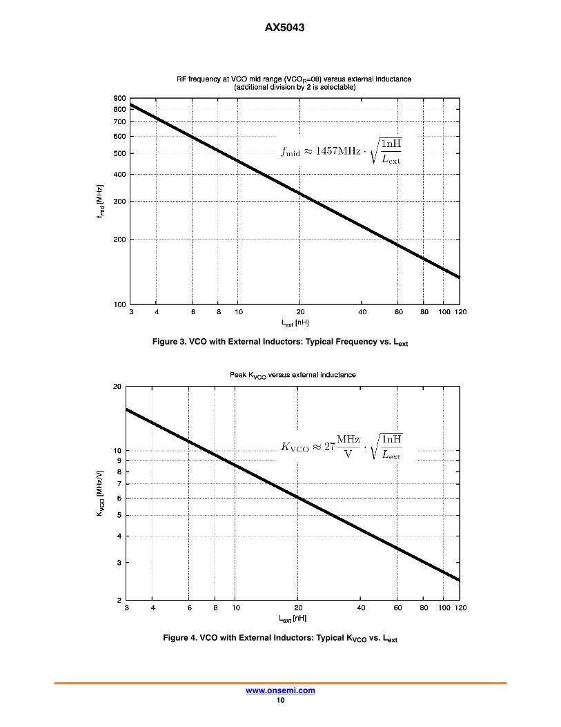
fRFrng_lo RF frequency rangeFor choice of Lext values as well asVCO gains see Figure 3 and Figure 4
RFDIV = 1 27 262 MHz
fRFrng_hi RFDIV = 0 54 525
PN169 Synthesizer phase noise 169 MHzLext=47 nH (wire wound 0603)RFDIV = 0, fREF= 16 MHzNote: phase noises can be im-proved with higher fREF
10 kHz from carrier −97 dBc/Hz
1 MHz from carrier −115
External VCO (VCOSEL = 1, VCO2INT = 0)
fRF RF frequency range fully externalVCO
Note: The external VCO frequency needsto be 2 x fRF
27 1000 MHz
Vamp Differential input amplitude at L1, L2terminals
0.7 V
VinL Input voltage levels at L1, L2 termi-nals
0 1.8 V
Vctrl Control voltage range Available at FILT in external loop filtermode
0 1.8 V
AX5043
www.onsemi.com10
Figure 3. VCO with External Inductors: Typical Frequency vs. Lext
Figure 4. VCO with External Inductors: Typical KVCO vs. Lext

AX5043
www.onsemi.com11
The following table shows the typical frequency rangesfor frequency synthesis with external VCO inductor fordifferent inductor values.
Table 9.
Lext [nH]
Freq [MHz]
RFDIV = 0
Freq [MHz]
RFDIV = 1 PLL Range
8.2 482 241 0
8.2 437 219 15
10 432 216 0
10 390 195 15
12 415 208 0
12 377 189 15
15 380 190 0
15 345 173 15
18 345 173 0
18 313 157 15
22 308 154 0
22 280 140 14
27 285 143 0
27 258 129 15
33 260 130 0
33 235 118 15
39 245 123 0
39 223 112 14
47 212 106 0
47 194 97 14
56 201 101 0
56 182 91 15
68 178 89 0
68 161 81 15
82 160 80 1
82 146 73 14
100 149 75 1
100 136 68 14
120 136 68 0
120 124 62 14
For tuning or changing of ranges a capacitor can be addedin parallel to the inductor.
AX5043
www.onsemi.com12
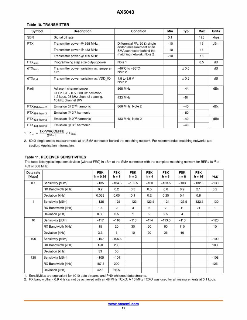
Table 10. TRANSMITTER
Symbol Description Condition Min Typ Max Units
SBR Signal bit rate 0.1 125 kbps
PTX Transmitter power @ 868 MHz Differential PA, 50 � singleended measurement at anSMA connector behind thematching network, Note 2
−10 16 dBm
Transmitter power @ 433 MHz −10 16
Transmitter power @ 169 MHz −10 16
PTXstep Programming step size output power Note 1 0.5 dB
dTXtemp Transmitter power variation vs. tempera-ture
−40°C to +85°CNote 2
± 0.5 dB
dTXVdd Transmitter power variation vs. VDD_IO 1.8 to 3.6 VNote 2
± 0.5 dB
Padj Adjacent channel powerGFSK BT = 0.5, 500 Hz deviation, 1.2 kbps, 25 kHz channel spacing, 10 kHz channel BW
868 MHz −44 dBc
433 MHz −51
PTX868−harm2 Emission @ 2nd harmonic 868 MHz, Note 2 −40 dBc
PTX868−harm3 Emission @ 3rd harmonic −60
PTX433−harm2 Emission @ 2nd harmonic 433 MHz, Note 2 −40 dBc
PTX433−harm3 Emission @ 3rd harmonic −40
1. Pout �TXPWRCOEFFB
212�1� Pmax
2. 50 � single ended measurements at an SMA connector behind the matching network. For recommended matching networks see
section: Application Information.
Table 11. RECEIVER SENSITIVITIES The table lists typical input sensitivities (without FEC) in dBm at the SMA connector with the complete matching network for BER=10−3 at433 or 868 MHz.
Data rate[kbps]
FSKh = 0.66
FSKh = 1
FSKh = 2
FSKh = 4
FSKh = 5
FSKh = 8
FSKh = 16 PSK
0.1 Sensitivity [dBm] −135 −134.5 −132.5 −133 −133.5 −133 −132.5 −138
RX Bandwidth [kHz] 0.2 0.2 0.3 0.5 0.6 0.9 2.1 0.2
Deviation [kHz] 0.033 0.05 0.1 0.2 0.25 0.4 0.8
1 Sensitivity [dBm] −126 −125 −123 −123.5 −124 −123.5 −122.5 −130
RX Bandwidth [kHz] 1.5 2 3 6 7 11 21 1
Deviation [kHz] 0.33 0.5 1 2 2.5 4 8
10 Sensitivity [dBm] −117 −116 −113 −114 −113.5 −113 −120
RX Bandwidth [kHz] 15 20 30 50 60 110 10
Deviation [kHz] 3.3 5 10 20 25 40
100 Sensitivity [dBm] −107 −105.5 −109
RX Bandwidth [kHz] 150 200 100
Deviation [kHz] 33 50
125 Sensitivity [dBm] −105 −104 −108
RX Bandwidth [kHz] 187.5 200 125
Deviation [kHz] 42.3 62.5
1. Sensitivities are equivalent for 1010 data streams and PN9 whitened data streams.2. RX bandwidths < 0.9 kHz cannot be achieved with an 48 MHz TCXO. A 16 MHz TCXO was used for all measurements at 0.1 kbps.

AX5043
www.onsemi.com13
Table 12. RECEIVER
Symbol Description Condition Min Typ Max Units
SBR Signal bit rate 0.1 125 kbps
ISBER868 Input sensitivity at BER = 10−3
for 868 MHz operation,continuous data,without FEC
FSK, h = 0.5, 100 kbps −106 dBm
FSK, h = 0.5, 10 kbps −116
FSK, 500 Hz deviation, 1.2 kbps −126
PSK, 100 kbps −109
PSK, 10 kbps −120
PSK, 1 kbps −130
ISBER868FEC Input sensitivity at BER = 10−3,for 868 MHz operation, continu-ous data,with FEC
FSK, h = 0.5, 50 kbps −111 dBm
FSK, h = 0.5, 5 kbps −122
FSK, 500 Hz deviation, 0.1 kbps −137
ISPER868 Input sensitivity at PER = 1%,for 868 MHz operation, 144 bitpacket data, without FEC
FSK, h = 0.5, 100 kbps −103 dBm
FSK, h = 0.5, 10 kbps −115
FSK, 1.2 kbps −125
ISWOR868 Input sensitivity at PER = 1% for 868 MHz operation, 144 bitpacket data, WOR−mode, with-out FEC
FSK, h = 0.5, 100 kpbs −102 dBm
IL Maximum input level Full selectivity 0 dBm
ILmax Maximum input level FSK, reduced selectivity 10
CP1dB Input referred compression point 2 tones separated by 100 kHz −35 dBm
RSSIR RSSI control range FSK, 500 Hz deviation, 1.2 kbps −126 −46 dB
RSSIS1 RSSI step size Before digital channel filter; calculatedfrom register AGCCOUNTER
0.625 dB
RSSIS2 RSSI step size Behind digital channel filter; calculatedfrom registers AGCCOUNTER, TRKAM-PL
0.1 dB
RSSIS3 RSSI step size Behind digital channel filter; reading reg-ister RSSI
1 dB
SEL868 Adjacent channel suppression 25 kHz channels , Note 1 45 dB
100 kHz channels, Note 1 47
BLK868 Blocking at ± 10 MHz offset Note 2 78 dB
RAFC AFC pull−in range The AFC pull−in range can be pro-grammed with the MAXRFOFFSET reg-isters.The AFC response time can be pro-grammed with the FREQGAIND regis-ter.
± 15 %
RDROFF Bitrate offset pull−in range The bitrate pull−in range can be pro-grammed with the MAXDROFFSET reg-isters.
± 10 %
1. Interferer/Channel @ BER = 10−3, channel level is +3 dB above the typical sensitivity, the interfering signal is CW; channel signal ismodulated with shaping
2. Channel/Blocker @ BER = 10−3, channel level is +3 dB above the typical sensitivity, the blocker signal is CW; channel signal is modulatedwith shaping
AX5043
www.onsemi.com14
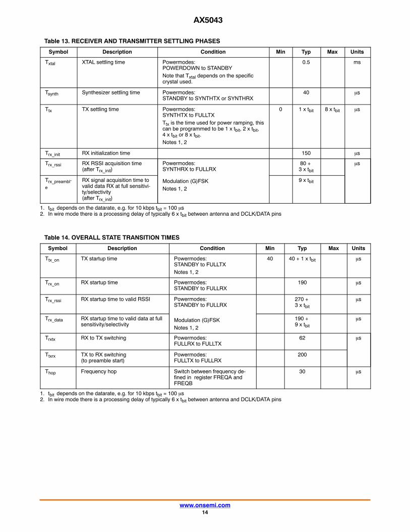
Table 13. RECEIVER AND TRANSMITTER SETTLING PHASES
Symbol Description Condition Min Typ Max Units
Txtal XTAL settling time Powermodes:POWERDOWN to STANDBYNote that Txtal depends on the specificcrystal used.
0.5 ms
Tsynth Synthesizer settling time Powermodes:STANDBY to SYNTHTX or SYNTHRX
40 �s
Ttx TX settling time Powermodes:SYNTHTX to FULLTXTtx is the time used for power ramping, thiscan be programmed to be 1 x tbit, 2 x tbit, 4 x tbit or 8 x tbit.Notes 1, 2
0 1 x tbit 8 x tbit �s
Trx_init RX initialization time 150 �s
Trx_rssi RX RSSI acquisition time(after Trx_init)
Powermodes:SYNTHRX to FULLRX
Modulation (G)FSKNotes 1, 2
80 + 3 x tbit
�s
Trx_preambl-
e
RX signal acquisition time tovalid data RX at full sensitivi-ty/selectivity(after Trx_init)
9 x tbit
1. tbit depends on the datarate, e.g. for 10 kbps tbit = 100 �s2. In wire mode there is a processing delay of typically 6 x tbit between antenna and DCLK/DATA pins
Table 14. OVERALL STATE TRANSITION TIMES
Symbol Description Condition Min Typ Max Units
Ttx_on TX startup time Powermodes:STANDBY to FULLTXNotes 1, 2
40 40 + 1 x tbit �s
Trx_on RX startup time Powermodes:STANDBY to FULLRX
190 �s
Trx_rssi RX startup time to valid RSSI Powermodes:STANDBY to FULLRX
Modulation (G)FSKNotes 1, 2
270 + 3 x tbit
�s
Trx_data RX startup time to valid data at fullsensitivity/selectivity
190 + 9 x tbit
�s
Trxtx RX to TX switching Powermodes:FULLRX to FULLTX
62 �s
Ttxrx TX to RX switching(to preamble start)
Powermodes:FULLTX to FULLRX
200
Thop Frequency hop Switch between frequency de-fined in register FREQA andFREQB
30 �s
1. tbit depends on the datarate, e.g. for 10 kbps tbit = 100 �s2. In wire mode there is a processing delay of typically 6 x tbit between antenna and DCLK/DATA pins

AX5043
www.onsemi.com15
Table 15. SPI TIMING
Symbol Description Condition Min Typ Max Units
Tss SEL falling edge to CLK rising edge 10 ns
Tsh CLK falling edge to SEL rising edge 10 ns
Tssd SEL falling edge to MISO driving 0 10 ns
Tssz SEL rising edge to MISO high−Z 0 10 ns
Ts MOSI setup time 10 ns
Th MOSI hold time 10 ns
Tco CLK falling edge to MISO output 10 ns
Tck CLK period Note 1 50 ns
Tcl CLK low duration 40 ns
Tch CLK high duration 40 ns
1. For SPI access during power−down mode the period should be relaxed to 100 ns
For a figure showing the SPI timing parameters see section: Serial Peripheral Interface (SPI).
Table 16. WIRE MODE INTERFACE TIMING
Symbol Description Condition Min Typ Max Units
Tdck SEL falling edge to CLK rising edge Depends on bit rate pro-gramming
1.6 10,000 �s
Tdcl DCLK low duration 25 75 %
Tdch DCLK high duration 25 75 %
Tds DATA setup time relative to activeDCLK edge
10 ns
Tdh DATA hold time relative to activeDCLK edge
10 ns
Tdco DATA output change relative to activeDCLK edge
10 ns
For a figure showing the wire mode interface timing parameters see section: Wire Mode Interface.
Table 17. GENERAL PURPOSE ADC (GPADC)
Symbol Description Condition Min Typ Max Units
Res Nominal ADC resolution 10 bit
Fconv Conversion rate 0.03 1 MS/s
DR Dynamic range 60 dB
INL Integral nonlinearity ± 1 LSB
DNL Differential nonlinearity ± 1 LSB
Zin Input impedance 50 k�
VDC−IN Input DC level 0.8 V
VIN−DIFF Input signal range (differential) −500 500 mV
VIN−SE Input signal range (single−ended, sig-nal input at pin GPADC1, pin GPADC2 open)
300 1300 mV
AX5043
www.onsemi.com16
CIRCUIT DESCRIPTION
The AX5043 is a true single chip ultra−low powernarrow−band CMOS transceiver for use in licensed andunlicensed bands from 27 and 1050 MHz. The on−chiptransceiver consists of a fully integrated RF front−end withmodulator, and demodulator. Base band data processing isimplemented in an advanced and flexible communicationcontroller that enables user friendly communication via theSPI interface.
AX5043 can be operated from a 1.8 V to 3.6 V powersupply over a temperature range of −40°C to 85°C. Itconsumes 7 − 48 mA for transmitting at 868 MHz carrierfrequency, 4 – 51 mA for transmitting at 169 MHzdepending on the output power. In receive operation AX5043 consumes 9 − 11 mA at 868 MHz carrier frequency and6.5 − 8.5 mA at 169 MHz.
The AX5043 features make it an ideal interface forintegration into various battery powered solutions such asticketing or as transceiver for telemetric applications e.g. insensors. As primary application, the transceiver is intendedfor UHF radio equipment in accordance with the EuropeanTelecommunication Standard Institute (ETSI) specificationEN 300 220−1 and the US Federal CommunicationsCommission (FCC) standard Title 47 CFR Part 15 as well asPart 90. AX5043 is compliant with respective narrow−bandregulations. Additionally AX5043 is suited for systemstargeting compliance with Wireless M−Bus standard EN13757−4:2005. Wireless M−Bus frame support (S, T, R) isbuilt−in.
AX5043 supports any data rate from 0.1 kbps to 125 kbpsfor FSK, 4−FSK, GFSK, GMSK, MSK, ASK and PSK. Toachieve optimum performance for specific data rates andmodulation schemes several register settings to configurethe AX5043 are necessary, for details see the AXSEMRadioLab Software which calculates the necessary registersettings and the AX5043 Programming Manual.
The AX5043 can be operated in two fundamentallydifferent modes.
In frame mode data is sent and received via the SPI portin frames. Pre− and post−ambles as well as checksums canbe generated automatically. Interrupts control the data flowbetween a micro−controller and the AX5043.
In wire mode the IC behaves as an extension of any wire.The internal communication controller is disabled and themodem data is directly available on a dedicated pin (DATA).The bit clock is also output on a dedicated pin (DCLK). Inthis mode the user can connect the data pin to any port of amicro−controller or to a UART, but has to control coding,checksums, pre and post ambles. The user can choosebetween synchronous and asynchronous wire mode,asynchronous wire mode performs RS232 start bitrecognition and re−synchronization for transmit.
Both modes can be used both for transmit and receive. Inboth cases the AX5043 behaves as a SPI slave interface.Configuration of the AX5043 is always done via the SPIinterface.
The receiver and the transmitter support multi−channeloperation for all data rates and modulation schemes.
Voltage RegulatorsThe AX5043 uses an on−chip voltage regulator system to
create stable supply voltages for the internal circuitry fromthe primary supply VDD_IO. The I/O level of the digitalpins is VDD_IO.
Pins VDD_ANA are supplied for external decoupling ofthe power supply used for the on−chip PA.
The voltage regulator system must be set into theappropriate state before receive or transmit operations canbe initiated. This is handled automatically whenprogramming the device modes via the PWRMODEregister.
Register POWSTAT contains status bits that can be readto check if the regulated voltages are ready (bit SVIO) or ifVDD_IO has dropped below the brown−out level of 1.3V(bit SSUM).
In power−down mode the core supply voltages for digitaland analog functions are switched off to minimize leakagepower. Most register contents are preserved but access to theFIFO is not possible and FIFO contents are lost. SPI accessto registers is possible, but at lower speed.
In deep−sleep mode all supply voltages are switched off.All digital and analog functions are disabled. All registercontents are lost. To leave deep−sleep mode the pin SEL hasto be pulled low. This will initiate startup and reset of theAX5043. Then the MISO line should be polled, as it will beheld low during initialization and will rise to high at the endof the initialization, when the chip becomes ready foroperation.
Crystal Oscillator and TCXO InterfaceThe AX5043 is normally operated with an external
TCXO, which is required by most narrow−band regulationwith a tolerance of 0.5 ppm to 1.5 ppm depending on theregulation. The on−chip crystal oscillator allows the use ofan inexpensive quartz crystal as the RF generationsubsystem’s timing reference when possible from aregulatory point of view.
A wide range of crystal frequencies can be handled by thecrystal oscillator circuit. As the reference frequency impactsboth the spectral performance of the transmitter as well asthe current consumption of the receiver, the choice ofreference frequency should be made according to theregulatory regime targeted by the application. Forguidelines see the separate Application Notes for usage ofAX5043 in compliance with various regulatory regimes.
The crystal or TCXO reference frequency should bechosen so that the RF carrier frequency is not an integermultiple of the crystal or TCXO frequency.
The oscillator circuit is enabled by programming thePWRMODE register. At power−up it is enabled.
AX5043
www.onsemi.com17
To adjust the circuit’s characteristics to the quartz crystalbeing used, without using additional external components,the tuning capacitance of the crystal oscillator can beprogrammed. The transconductance of the oscillator isautomatically regulated, to allow for fastest start−up timestogether with lowest power operation during steady−stateoscillation.
The integrated programmable tuning capacitor bankmakes it possible to connect the oscillator directly to pinsCLK16N and CLK16P without the need for externalcapacitors. It is programmed using bits XTALCAP[5:0] inregister XTALCAP.
To synchronize the receiver frequency to a carrier signal,the oscillator frequency could be tuned using the capacitorbank however, the recommended method to implementfrequency synchronization is to make use of the highresolution RF frequency generation sub−system togetherwith the Automatic Frequency Control, both are describedfurther down.
Alternatively a single ended reference (TXCO, CXO)may be used. For detailed TCXO network recommendationsdepending on TCXO output swing refer to the AX5043Application Note: Use with a TCXO Reference Clock.
Low Power Oscillator and Wake−on−Radio (WOR)Mode
The AX5043 features an internal lowest power fullyintegrated oscillator. In default mode the frequency of
oscillation is 640 Hz ± 1.5%, in fast mode it is 10.2 kHz ±1.5%. These accuracies are reached after the internalhardware has been used to calibrate the low power oscillatorversus the RF reference clock. This procedure can be run inthe background during transmit or receive operations.
The low power oscillator makes a WOR mode with apower consumption of 500 nA possible.
If Wake on Radio Mode is enabled, the receiver wakes upperiodically at a user selectable interval, and checks for aradio signal on the selected channel. If no signal is detected,the receiver shuts down again. If a radio signal is detected,and a valid packet is received, the microcontroller is alertedby asserting an interrupt.
The AX5043 can thus autonomously poll for radiosignals, while the micro−controller can stay powered down,and only wakes up once a valid packet is received. Thisallows for very low average receiver power, at the expenseof longer preambles at the transmitter.
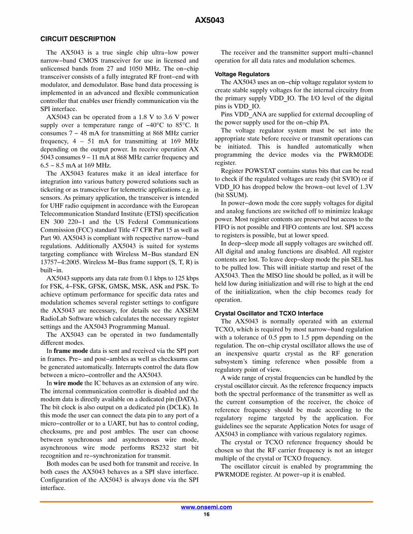
GPIO PinsPins DATA, DCLK, SYSCLK, IRQ, ANTSEL,
PWRAMP can be used as general purpose I/O pins byprogramming pin configuration registersPINFUNCSYSCLK, PINFUNCDCLK, PINFUNCDATA,PINFUNCIRQ, PINFUNCNANTSEL,PINFUNCPWRAMP. Pin input values can be read viaregister PINSTATE. Pull−ups are disabled if output data isprogrammed to the GPIO pin.
Figure 5. GPIO Pin
65 k�
VDD_IO
VDD_IO
output data
input data
enable weak pull−up
enable output

AX5043
www.onsemi.com18
SYSCLK OutputThe SYSCLK pin outputs either the reference clock signal
divided by a programmable power of two or the low poweroscillator clock. Division ratios from 1 to 1024 are possible.For divider ratios > 1 the duty cycle is 50%. BitsSYSCLK[4:0] in the PINFUNCSYSCLK register set thedivider ratio. The SYSCLK output can be disabled.
After power−up SYSCLK outputs 1/16 of the crystaloscillator clock, making it possible to use this clock to boota micro−controller.
Power−on−Reset (POR)AX5043 has an integrated power−on−reset block. No
external POR circuit is required.After POR the AX5043 can be reset by first setting the SPI
SEL pin to high for at least 100 ns, then setting followed byresetting the bit RST in the PWRMODE register.
After POR or reset all registers are set to their defaultvalues.
RF Frequency Generation SubsystemThe RF frequency generation subsystem consists of a
fully integrated synthesizer, which multiplies the referencefrequency from the crystal oscillator to get the desired RFfrequency. The advanced architecture of the synthesizerenables frequency resolutions of 1 Hz, as well as fast settlingtimes of 5 – 50 �s depending on the settings (see section ACCharacteristics). Fast settling times mean fast start−up andfast RX/TX switching, which enables low−power systemdesign.
For receive operation the RF frequency is fed to the mixer,for transmit operation to the power−amplifier.
The frequency must be programmed to the desired carrierfrequency.
The synthesizer loop bandwidth can be programmed, thisserves three purposes:
1. Start−up time optimization, start−up is faster forhigher synthesizer loop bandwidths
2. TX spectrum optimization, phase−noise at300 kHz to 1 MHz distance from the carrierimproves with lower synthesizer loop bandwidths
3. Adaptation of the bandwidth to the data−rate. Fortransmission of FSK and MSK it is required thatthe synthesizer bandwidth must be in the order ofthe data−rate.
VCOAn on−chip VCO converts the control voltage generated
by the charge pump and loop filter into an output frequency.This frequency is used for transmit as well as for receiveoperation. The frequency can be programmed in 1 Hz stepsin the FREQ registers. For operation in the 433 MHz band,the RFDIV bit in the PLLVCODIV register must beprogrammed.
The fully integrated VCO allows to operate the device inthe frequency ranges 800 – 1050 MHz and 400 – 525 MHz.
The carrier frequency range can be extended to 54 –525 MHz and 27 – 262 MHz by using an appropriateexternal inductor between device pins L1 and L2. The bitVCO2INT in the PLLVCODIV register must be set high toenter this mode.
It is also possible to use a fully external VCO by settingbits VCO2INT = 0 and VCOSEL = 1 in the PLLVCODIVregister. A differential input at a frequency of double thedesired RF frequency must be input at device pins L1 andL2. The control voltage for the VCO can be output at devicepin FILT when using external filter mode. The voltage rangeof this output pin is 0 – 1.8 V.
This mode of operation is recommended for specialapplications where the phase noise requirements are not metwhen using the fully internal VCO or the internal VCO withexternal inductor.
VCO Auto−RangingThe AX5043 has an integrated auto−ranging function,
which allows to set the correct VCO range for specificfrequency generation subsystem settings automatically.Typically it has to be executed after power−up. The functionis initiated by setting the RNG_START bit in thePLLRANGINGA or PLLRANGINGB register. The bit isreadable and a 0 indicates the end of the ranging process.Setting RNG_START in the PLLRANGINGA registerranges the frequency in FREQA, while settingRNG_START in the PLLRANGINGB register ranges thefrequency in FREQB. The RNGERR bit indicates thecorrect execution of the auto−ranging.
VCO auto−ranging works with the fully integrated VCOand with the internal VCO with external inductor.
Loop Filter and Charge PumpThe AX5043 internal loop filter configuration together
with the charge pump current sets the synthesizer loop bandwidth. The internal loop−filter has three configurations thatcan be programmed via the register bits FLT[1:0] in registersPLLLOOP or PLLLOOPBOOST the charge pump currentcan be programmed using register bits PLLCPI[7:0] inregisters PLLCPI or PLLCPIBOOST. Synthesizerbandwidths are typically 50 – 500 kHz depending on thePLLLOOP or PLLLOOPBOOST settings, for details seethe section: AC Characteristics.
The AX5043 can be setup in such a way that when thesynthesizer is started, the settings in the registersPLLLOOPBOOST and PLLCPIBOOST are applied firstfor a programmable duration before reverting to the settingsin PLLLOOP and PLLCPI. This feature enables automatedfastest start−up.
Setting bits FLT[1:0] = 00 bypasses the internal loop filterand the VCO control voltage is output to an external loopfilter at pin FILT. This mode of operation is recommendedfor achieving lower bandwidths than with the internal loopfilter and for usage with a fully external VCO.
AX5043
www.onsemi.com19
Registers
Table 18. RF FREQUENCY GENERATION REGISTERS
Register Bits Purpose
PLLLOOPPLLLOOPBOOST
FLT[1:0] Synthesizer loop filter bandwidth and selection of external loop filter, recommended usage is toincrease the bandwidth for faster settling time, bandwidth increases of factor 2 and 5 are possi-ble.
PLLCPIPLLCPIBOOST
Synthesizer charge pump current, recommended usage is to decrease the bandwidth (andimprove the phase−noise) for low data−rate transmissions.
PLLVCODIV REFDIV Sets the synthesizer reference divider ratio.
RFDIV Sets the synthesizer output divider ratio.
VCOSEL Selects either the internal or the external VCO
VCO2INT Selects either the internal VCO inductor or an external inductor between pins L1 and L2
FREQA, FREQB Programming of the carrier frequency
PLLRANGINGA, PLLRANGINGB Initiate VCO auto−ranging and check results
RF Input and Output Stage (ANTP/ANTN/ANTP1)The AX5043 has two main antenna interface modes:
1. Both RX and TX use differential pins ANTP andANTN. RX/TX switching is handled internally.This mode is recommended for highest outputpowers, highest sensitivities and for directconnection to dipole antennas. Also see Figure 13.
2. RX uses the differential antenna pins ANTP andANTN. TX uses the single ended antenna pinANTP1. RX/TX switching is handled externally.This can be done either with an external RX/TXswitch or with a direct tie configuration. Thismode is recommended for low output powers athigh efficiency (Figure 16) and for usage withexternal power amplifiers (Figure 15).
Pin PWRAMP can be used to control an external RX/TXswitch when operating the device together with an externalPA (Figure 15). Pin ANTSEL can be used to control anexternal antenna switch when receiving with two antennas(Figure 17).
When antenna diversity is enabled, the radio controllerwill, when not in the middle of receiving a packet,periodically probe both antennas and select the antenna withthe highest signal strength. The radio controller can beinstructed to periodically write both RSSI values into theFIFO. Antenna diversity mode is fully automatic.
LNAThe LNA amplifies the differential RF signal from the
antenna and buffers it to drive the I/Q mixer. An externalmatching network is used to adapt the antenna impedance tothe IC impedance. A DC feed to GND must be provided atthe antenna pins. For recommendations see section:Application Information.
PAIn TX mode the PA drives the signal generated by the
frequency generation subsystem out to either the differentialantenna terminals or to the single ended antenna pin. Theantenna terminals are chosen via the bits TXDIFF and TXSEin register MODECFGA.
The output power of the PA is programmed via the registerTXPWRCOEFFB.
The PA can be digitally pre−distorted for high linearity.The output amplitude can be shaped (raised cosine), this
mode is selected with bit AMPLSHAPE in registerMODECFGA. PA ramping is programmable in incrementsof the bit time and can be set to 1 – 8 bit times via bitsSLOWRAMP in register MODECFGA.
Output power as well as harmonic content will depend onthe external impedance seen by the PA, recommendationsare given in the section: Application Information.
Digital IF Channel Filter and DemodulatorThe digital IF channel filter and the demodulator extract
the data bit−stream from the incoming IF signal. They mustbe programmed to match the modulation scheme as well asthe data−rate. Inaccurate programming will lead to loss ofsensitivity.
The channel filter offers bandwidths of 995 Hz up to221 kHz.
The AXSEM RadioLab Software calculates the necessaryregister settings for optimal performance and details can befound in the AX5043 Programming Manual. An overviewof the registers involved is given in the following table asreference. The register setups typically must be done onceat power−up of the device.

AX5043
www.onsemi.com20
Registers
Table 19. CHANNEL FILTER AND DEMODULATOR REGISTERS
Register Remarks
DECIMATION This register programs the bandwidth of the digital channel filter.
RXDATARATE2… RXDATARATE0 These registers specify the receiver bit rate, relative to the channel filter bandwidth.
MAXDROFFSET2… MAXDROFFSET0 These registers specify the maximum possible data rate offset.
MAXRFOFFSET2… MAXRFOFFSET0 These registers specify the maximum possible RF frequency offset.
TIMEGAIN, DRGAIN These registers specify the aggressiveness of the receiver bit timing recovery. Moreaggressive settings allow the receiver to synchronize with shorter preambles, at theexpense of more timing jitter and thus a higher bit error rate at a given signal−to−noiseratio.
MODULATION This register selects the modulation to be used by the transmitter and the receiver, i.e. whether ASK, FSK should be used.
PHASEGAIN, FREQGAINA, FREQGAINB, FRE-QGAINC, FREQGAIND, AMPLGAIN
These registers control the bandwidth of the phase, frequency offset and amplitudetracking loops.
AGCGAIN This register controls the AGC (automatic gain control) loop slopes, and thus thespeed of gain adjustments. The faster the bit−rate, the faster the AGC loop should be.
TXRATE These registers control the bit rate of the transmitter.
FSKDEV These registers control the frequency deviation of the transmitter in FSK mode. Thereceiver does not explicitly need to know the frequency deviation, only the channelfilter bandwidth has to be set wide enough for the complete modulation to pass.
EncoderThe encoder is located between the Framing Unit, the
Demodulator and the Modulator. It can optionally transformthe bit−stream in the following ways:• It can invert the bit stream.
• It can perform differential encoding. This means that azero is transmitted as no change in the level, and a oneis transmitted as a change in the level.
• It can perform Manchester encoding. Manchesterencoding ensures that the modulation has no DCcontent and enough transitions (changes from 0 to 1 andfrom 1 to 0) for the demodulator bit timing recovery tofunction correctly, but does so at a doubling of the datarate.
• It can perform spectral shaping (also know aswhitening). Spectral shaping removes DC content ofthe bit stream, ensures transitions for the demodulatorbit timing recovery, and makes sure that the transmittedspectrum does not have discrete lines even if thetransmitted data is cyclic. It does so without addingadditional bits, i.e. without changing the data rate.Spectral Shaping uses a self synchronizing feedbackshift register.
The encoder is programmed using the registerENCODING, details and recommendations on usage aregiven in the AX5043 Programming Manual.
Framing and FIFOMost radio systems today group data into packets. The
framing unit is responsible for converting these packets into
a bit−stream suitable for the modulator, and to extractpackets from the continuous bit−stream arriving from thedemodulator.
The Framing unit supports two different modes:• Packet modes
• Raw modesThe micro−controller communicates with the framing
unit through a 256 byte FIFO. Data in the FIFO is organizedin Chunks. The chunk header encodes the length and whatdata is contained in the payload. Chunks may contain packetdata, but also RSSI, Frequency offset, Timestamps, etc.
The AX5043 contains one FIFO. Its direction is switcheddepending on whether transmit or receive mode is selected.
The FIFO can be operated in polled or interrupt drivenmodes. In polled mode, the microcontroller mustperiodically read the FIFO status register or the FIFO countregister to determine whether the FIFO needs servicing.
In interrupt mode EMPTY, NOT EMPTY, FULL, NOTFULL and programmable level interrupts are provided. TheAX5043 signals interrupts by asserting (driving high) itsIRQ line. The interrupt line is level triggered, active high.Interrupts are acknowledged by removing the cause for theinterrupt, i.e. by emptying or filling the FIFO.
Basic FIFO status (EMPTY, FULL, Overrun, Underrun,FIFO fill level above threshold, FIFO free space abovethreshold) are also provided during each SPI access onMISO while the micro− controller shifts out the registeraddress on MOSI. See the SPI interface section for details.This feature significantly reduces the number of SPIaccesses necessary during transmit and receive.
AX5043
www.onsemi.com21
Packet ModesThe AX5043 offers different packet modes. For arbitrary
packet sizes HDLC is recommended since the flag andbit−stuffing mechanism. The AX5043 also offers packetmodes with fixed packet length with a byte indicating thelength of the packet.
In packet modes a CRC can be computed automatically.HDLC Mode is the main framing mode of the AX5043. In
this mode, the AX5043 performs automatic packet
delimiting, and optional packet correctness check byinserting and checking a cyclic redundancy check (CRC)field.
NOTE: HDLC mode follows High−Level Data LinkControl (HDLC, ISO 13239) protocol.
The packet structure is given in the following table.
Table 20. HDLC PACKET STRUCTURE
Flag Address Control Information FCS (Optional Flag)
8 bit 8 bit 8 or 16 bit Variable length, 0 or more bits in multiples of 8 16 / 32 bit 8 bit
HDLC packets are delimited with flag sequences ofcontent 0x7E.
In AX5043 the meaning of address and control is userdefined. The Frame Check Sequence (FCS) can beprogrammed to be CRC−CCITT, CRC−16 or CRC−32.
The receiver checks the CRC, the result can be retrievedfrom the FIFO, the CRC is appended to the received data.
In Wireless M−Bus Mode, the packet structure is given inthe following table.NOTE: Wireless M−Bus mode follows EN13757−4
Table 21. WIRELESS M−BUS PACKET STRUCTURE
Preamble L C M A FCSOptional Data Block
(optionally repeated with FCS) FCS
variable 8 bit 8 bit 16 bit 48 bit 16 bit 8 − 96 bit 16 bit
For details on implementing a HDLC communication aswell as Wireless M−Bus please use the AXSEM RadioLabsoftware and see the AX5043 Programming Manual.
Raw ModesIn Raw mode, the AX5043 does not perform any packet
delimiting or byte synchronization. It simply serializestransmit bytes and de−serializes the received bit−stream andgroups it into bytes. This mode is ideal for implementinglegacy protocols in software.
Raw mode with preamble match is similar to raw mode.In this mode, however, the receiver does not receiveanything until it detects a user programmable bit pattern(called the preamble) in the receive bit−stream. When itdetects the preamble, it aligns the de−serialization to it.
The preamble can be between 4 and 32 bits long.
RX AGC and RSSIAX5043 features three receiver signal strength indicators
(RSSI):1. RSSI before the digital IF channel filter.
The gain of the receiver is adjusted in order tokeep the analog IF filter output level inside theworking range of the ADC and demodulator. Theregister AGCCOUNTER contains the current
value of the AGC and can be used as an RSSI. Thestep size of this RSSI is 0.625 dB. The value canbe used as soon as the RF frequency generationsub−system has been programmed.
2. RSSI behind the digital IF channel filter.The register RSSI contains the current value of theRSSI behind the digital IF channel filter. The stepsize of this RSSI is 1 dB.
3. RSSI behind the digital IF channel filter highaccuracy. The demodulator also provides amplitudeinformation in the TRK_AMPLITUDE register.By combining both the AGCCOUNTER and theTRK_AMPLITUDE registers, a high resolution(better than 0.1 dB) RSSI value can be computedat the expense of a few arithmetic operations onthe micro−controller. The AXSEM RadioLabSoftware calculates the necessary register settingsfor best performance and details can be found inthe AX5043 Programming Manual.
ModulatorDepending on the transmitter settings the modulator
generates various inputs for the PA:
AX5043
www.onsemi.com22
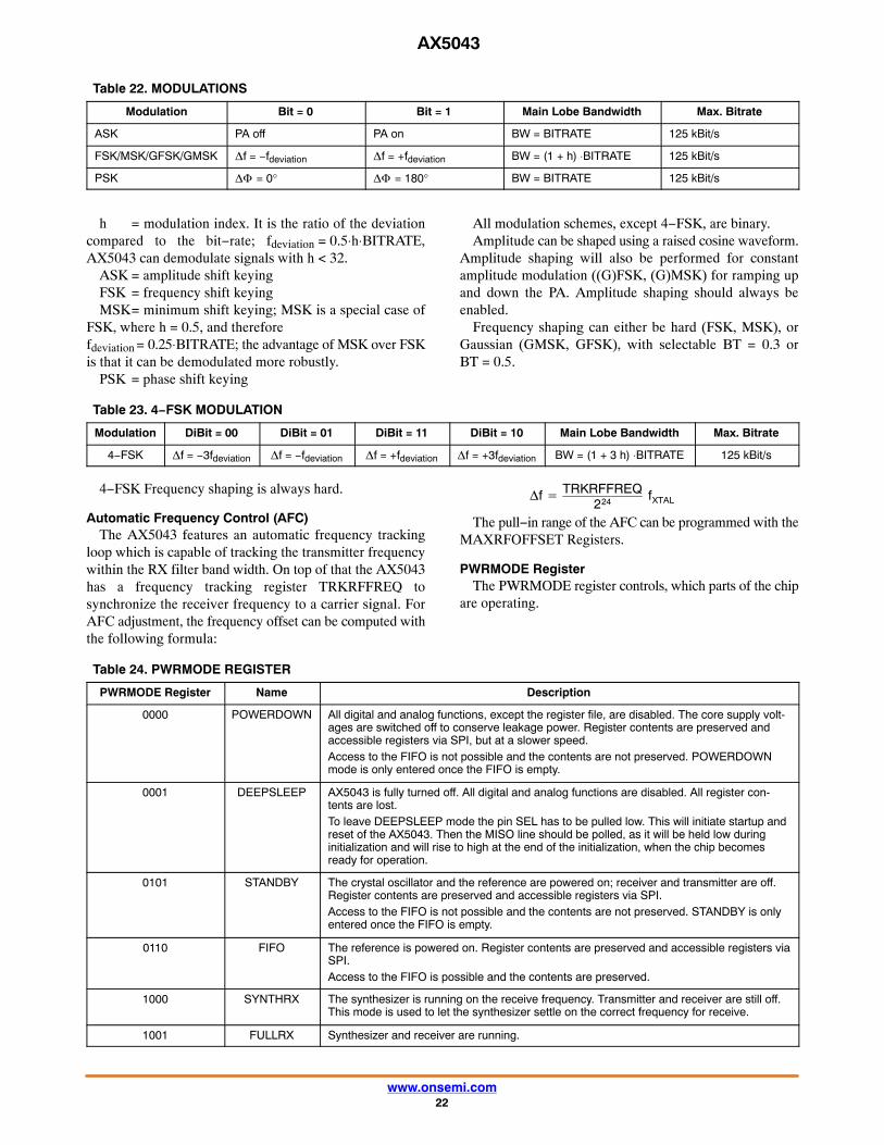
Table 22. MODULATIONS
Modulation Bit = 0 Bit = 1 Main Lobe Bandwidth Max. Bitrate
ASK PA off PA on BW = BITRATE 125 kBit/s
FSK/MSK/GFSK/GMSK �f = −fdeviation �f = +fdeviation BW = (1 + h) ⋅BITRATE 125 kBit/s
PSK �� = 0° �� = 180° BW = BITRATE 125 kBit/s
h = modulation index. It is the ratio of the deviationcompared to the bit−rate; fdeviation = 0.5⋅h⋅BITRATE,AX5043 can demodulate signals with h < 32.
ASK = amplitude shift keyingFSK = frequency shift keyingMSK= minimum shift keying; MSK is a special case of
FSK, where h = 0.5, and therefore fdeviation = 0.25⋅BITRATE; the advantage of MSK over FSKis that it can be demodulated more robustly.
PSK = phase shift keying
All modulation schemes, except 4−FSK, are binary.Amplitude can be shaped using a raised cosine waveform.
Amplitude shaping will also be performed for constantamplitude modulation ((G)FSK, (G)MSK) for ramping upand down the PA. Amplitude shaping should always beenabled.
Frequency shaping can either be hard (FSK, MSK), orGaussian (GMSK, GFSK), with selectable BT = 0.3 orBT = 0.5.
Table 23. 4−FSK MODULATION
Modulation DiBit = 00 DiBit = 01 DiBit = 11 DiBit = 10 Main Lobe Bandwidth Max. Bitrate
4−FSK �f = −3fdeviation �f = −fdeviation �f = +fdeviation �f = +3fdeviation BW = (1 + 3 h) ⋅BITRATE 125 kBit/s
4−FSK Frequency shaping is always hard.
Automatic Frequency Control (AFC)The AX5043 features an automatic frequency tracking
loop which is capable of tracking the transmitter frequencywithin the RX filter band width. On top of that the AX5043has a frequency tracking register TRKRFFREQ tosynchronize the receiver frequency to a carrier signal. ForAFC adjustment, the frequency offset can be computed withthe following formula:
�f � TRKRFFREQ224 fXTAL
The pull−in range of the AFC can be programmed with theMAXRFOFFSET Registers.
PWRMODE RegisterThe PWRMODE register controls, which parts of the chip
are operating.
Table 24. PWRMODE REGISTER
PWRMODE Register Name Description
0000 POWERDOWN All digital and analog functions, except the register file, are disabled. The core supply volt-ages are switched off to conserve leakage power. Register contents are preserved andaccessible registers via SPI, but at a slower speed.Access to the FIFO is not possible and the contents are not preserved. POWERDOWNmode is only entered once the FIFO is empty.
0001 DEEPSLEEP AX5043 is fully turned off. All digital and analog functions are disabled. All register con-tents are lost.To leave DEEPSLEEP mode the pin SEL has to be pulled low. This will initiate startup andreset of the AX5043. Then the MISO line should be polled, as it will be held low duringinitialization and will rise to high at the end of the initialization, when the chip becomesready for operation.
0101 STANDBY The crystal oscillator and the reference are powered on; receiver and transmitter are off.Register contents are preserved and accessible registers via SPI.Access to the FIFO is not possible and the contents are not preserved. STANDBY is onlyentered once the FIFO is empty.
0110 FIFO The reference is powered on. Register contents are preserved and accessible registers viaSPI.Access to the FIFO is possible and the contents are preserved.
1000 SYNTHRX The synthesizer is running on the receive frequency. Transmitter and receiver are still off.This mode is used to let the synthesizer settle on the correct frequency for receive.
1001 FULLRX Synthesizer and receiver are running.
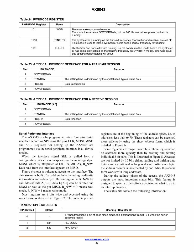
AX5043
www.onsemi.com23
Table 24. PWRMODE REGISTER
PWRMODE Register DescriptionName
1011 WOR Receiver wakeup−on−radio mode.The mode the same as POWERDOWN, but the 640 Hz internal low power oscillator isrunning.
1100 SYNTHTX The synthesizer is running on the transmit frequency. Transmitter and receiver are still off.This mode is used to let the synthesizer settle on the correct frequency for transmit.
1101 FULLTX Synthesizer and transmitter are running. Do not switch into this mode before the synthesiz-er has completely settled on the transmit frequency (in SYNTHTX mode), otherwise spuri-ous spectral transmissions will occur.
Table 25. A TYPICAL PWRMODE SEQUENCE FOR A TRANSMIT SESSION
Step PWRMODE Remarks
1 POWERDOWN
2 STANDBY The settling time is dominated by the crystal used, typical value 3ms.
3 FULLTX Data transmission
4 POWERDOWN
Table 26. A TYPICAL PWRMODE SEQUENCE FOR A RECEIVE SESSION
Step PWRMODE [3:0] Remarks
1 POWERDOWN
2 STANDBY The settling time is dominated by the crystal used, typical value 3ms.
3 FULLRX Data reception
4 POWERDOWN
Serial Peripheral InterfaceThe AX5043 can be programmed via a four wire serial
interface according SPI using the pins CLK, MOSI, MISOand SEL. Registers for setting up the AX5043 areprogrammed via the serial peripheral interface in all devicemodes.
When the interface signal SEL is pulled low, aconfiguration data stream is expected on the input signal pinMOSI, which is interpreted as D0...Dx, A0...Ax, R_N/W.Data read from the interface appears on MISO.
Figure 6 shows a write/read access to the interface. Thedata stream is built of an address byte including read/writeinformation and a data byte. Depending on the R_N/W bitand address bits A[6..0], data D[7..0] can be written viaMOSI or read at the pin MISO. R_N/W = 0 means readmode, R_N/W = 1 means write mode.
Most registers are 8 bits wide and accessed using thewaveforms as detailed in Figure 7. The most important
registers are at the beginning of the address space, i.e. ataddresses less than 0x70. These registers can be accessedmore efficiently using the short address form, which isdetailed in Figure 6.
Some registers are longer than 8 bits. These registers canbe accessed more quickly than by reading and writingindividual 8 bit parts. This is illustrated in Figure 8. Accessesare not limited by 16 bits either, reading and writing databytes can be continued as long as desired. After each byte,the address counter is incremented by one. Also, this accessform works with long addresses.
During the address phase of the access, the AX5043outputs the most important status bits. This feature isdesigned to speed up the software decision on what to do inan interrupt handler.
The status bits contain the following information:
Table 27. SPI STATUS BITS
SPI Bit Cell Status Meaning / Register Bit
0 −1 (when transitioning out of deep sleep mode, this bit transitions from 0 → 1 when the powerbecomes ready)
1 S14 PLL LOCK
2 S13 FIFO OVER

AX5043
www.onsemi.com24
Table 27. SPI STATUS BITS
SPI Bit Cell Meaning / Register BitStatus
3 S12 FIFO UNDER
4 S11 THRESHOLD FREE (FIFOFREE > FIFOTHRESH)
5 S10 THRESHOLD COUNT (FIFOCOUNT > FIFOTHRESH)
6 S9 FIFO FULL
7 S8 FIFO EMPTY
8 S7 PWRGOOD (not BROWNOUT)
9 S6 PWR INTERRUPT PENDING
10 S5 RADIO EVENT PENDING
11 S4 XTAL OSCILLATOR RUNNING
12 S3 WAKEUP INTERRUPT PENDING
13 S2 LPOSC INTERRUPT PENDING
14 S1 GPADC INTERRUPT PENDING
15 S0 internal
NOTE: Device will meet the specifications after thermal equilibrium has been established when mounted in a test socket or printed circuitboard with maintained transverse airflow greater than 500 lfpm.
SPI Timing
Figure 6. SPI 8 Bit Read/Write Access with Timing
Tsh
R/ W
SEL
CLK
MOSI
MISO
A6 A5 A4 A3 A2 A1 D7A0 D6 D5 D4 D0D1D2D3
D7 D6 D5 D4 D3 D2 D1 D0S14 S13 S12 S11 S10 S9 S8
Tssd Tco
Tss Tck TchTcl ThTs
Tssz
Figure 7. SPI 8 Bit Long Address Read/Write Access
R/W
SEL
CLK
MOSI
MISO
A6 A5 A4 A3 A2 A1 D7A0 D6 D5 D4 D0D1D2D3
D7 D6 D5 D4 D3 D2 D1 D0S6 S5 S4 S3 S2 S1 S0
A11 A10 A9 A7A8
S7S14 S13 S12 S11 S10 S9 S8
Figure 8. SPI 16 Bit Long Read/Write Access
R/W
SEL
CLK
MOSI
MISO
D6 D5 D4 D3 D2 D1 D7D0 D6 D5 D4 D0D1D2D3
D7 D6 D5 D4 D3 D2 D1 D0D6 D5 D4 D3 D2 D1 D0
A3 A2 A1 D7A0
D7S14 S13 S12 S11 S10 S9 S8
A6 A5 A4
Wire Mode InterfaceIn wire mode the transmitted or received data are
transferred from and to the AX5043 using the pins DATAand DCLK. DATA is an input when transmitting and anoutput when receiving.
The direction can be chosen by programming thePWRMODE register.
Wire mode offers two variants: synchronous orasynchronous.

AX5043
www.onsemi.com25
In synchronous wire mode the, the AX5043 always drivesDCLK. Transmit data must be applied to DATAsynchronously to DCLK, and receive data must be sampledsynchronously to DCLK. Timing is given in Figure 9. Inasynchronous wire mode, a low voltage RS232 type UARTcan be connected to DATA. DCLK is optional in this mode.The UART must be programmed to send two stop bits, butmust be able to accept only one stop bit. Both the UART datarate and the AX5043 transmit and receive bit rate mustmatch. The AX5043 synchronizes the RS232 signal to itsinternal transmission clock, by inserting or deleting a stopbit.
Wiremode is also available in 4−FSK mode. The two bitsthat encode one symbol are serialized on the DATA pin. ThePWRAMP pin can be used as a synchronisation pin to allowsymbol (dibit) boundaries to be reconstructed. Gray codingis used to reduce the number of bit errors in case of a wrongdecision. The AXSEM RadioLab software calculates thenecessary register settings for best performance and detailscan be found in the AX5043 Programming Manual.
Registers for setting up the AX5043 are programmed viathe serial peripheral interface (SPI).
Wire Mode Timing
Figure 9. Wire Mode Interface Timing
Tdh
DCLK (DCLKI=0)
DATA (RX)
DCLK (DCLKI=1)
Tdco
DATA (TX)
Tdch TdclTdck Tds
General Purpose ADC (GPADC)The AX5043 features a general purpose ADC. The ADC
input pins are GPADC1 and GPADC2. The ADC convertsthe voltage difference applied between pins GPADC1 andGPADC2. If pin GPADC2 is left open, the ADC converts thedifference between an internally generated value of 800 mVand the voltage applied at pin GPADC1.
The GPADC can only be used if the receiver is disabled.To enable the GPADC write 1 to the GPADC13 bit in theGPADCCTRL register. To start a single conversion, write 1to the BUSY bit in the GPADCCTRL register. Then wait forthe BUSY bit to clear, or the GPADC Interrupt to be asserted.
The GPADC Interrupt is cleared by reading the resultregister GPADC13VALUE.
If continuous sampling is desired, set the CONT bit inregister GPADCCTRL. The desired sampling rate can bespecified in the GPADCPERIOD register.
�� DACOne digital Pin (ANTSEL or PWRAMP) may be used as
a �� Digital−to−Analog Converter. A simple RC lowpassfilter is needed to smooth the output. The DAC may be usedto output RSSI, many demodulator variables, or a constantvalue under software control.

AX5043
www.onsemi.com26
REGISTER BANK DESCRIPTION
This section describes the bits of the register bank asreference. The registers are grouped by functional block tofacilitate programming. The AXSEM RadioLab softwarecalculates the necessary register settings for bestperformance and details can be found in the AX5043Programming Manual.
An R in the retention column means that this register’scontents are not lost during power−down mode.
No checks are made whether the programmedcombination of bits makes sense! Bit 0 is always the LSB.
NOTES: Whole registers or register bits marked asreserved should be kept at their default values.
All addresses not documented here must not beaccessed, neither in reading nor in writing.
The retention column indicates if the registercontents are preserved in power−down mode.
Table 28. CONTROL REGISTER MAP
Add Name Dir Ret Reset
Bit
Description7 6 5 4 3 2 1 0
Revision & Interface Probing
000 REVISION R R 01010001 SILICONREV(7:0) Silicon Revision
001 SCRATCH RW R 11000101 SCRATCH(7:0) Scratch Register
Operating Mode
002 PWRMODE RW R 011–0000 RST XOEN REFEN WDS PWRMODE(3:0) Power Mode
Voltage Regulator
003 POWSTAT R R –––––––– SSUM SREF SVREF SVANA SVMODEM SBEVANA SBEVMOD-EM
SVIO Power ManagementStatus
004 POWSTICKYST-AT
R R –––––––– SSSUM SREF SSVREF SSVANA SSVMODE-M
SSBEVANA SSBEVMO-DEM
SSVIO Power ManagementSticky Status
005 POWIRQMASK RW R 00000000 MPWRGOOD
MSREF MSVREF MS VANA MS VMO-DEM
MSBEVANA
MSBEVMODEM
MSVIO Power Management In-terrupt Mask
Interrupt Control
006 IRQMASK1 RW R ––000000 – – IRQMASK(13:8) IRQ Mask
007 IRQMASK0 RW R 00000000 IRQMASK(7:0) IRQ Mask
008 RADIOEVENTM-ASK1
RW R –––––––0 – – – – – – – RADIOEVENTMASK(8)
Radio Event Mask
009 RADIOEVENTM-ASK0
RW R 00000000 RADIO EVENT MASK(7:0) Radio Event Mask
00A IRQINVERSION1
RW R ––000000 – – IRQINVERSION(13:8) IRQ Inversion
00B IRQINVERSION0
RW R 00000000 IRQINVERSION(7:0) IRQ Inversion
00C IRQREQUEST1 R R –––––––– – – IRQREQUEST(13:8) IRQ Request
00D IRQREQUEST0 R R –––––––– IRQREQUEST(7:0) IRQ Request
00E RADIOEVENTR-EQ1
R –––––––– – – – – – – – RADIOEVENTREQ(8)
Radio Event Request
00F RADIOEVENTR-EQ0
R –––––––– RADIO EVENT REQ(7:0) Radio Event Request
Modulation & Framing
010 MODULATION RW R –––01000 – – – RX HALFSPEED
MODULATION(3:0) Modulation
011 ENCODING RW R –––00010 – – – ENCNOSYNC
ENCMANCH
ENCSCRAM
ENC DIFF ENC INV Encoder/Decoder Set-tings
012 FRAMING RW R –0000000 FRMRX CRCMODE(2:0) FRMMODE(2:0) FABORT Framing settings
014 CRCINIT3 RW R 11111111 CRCINIT(31:24) CRC Initialisation Data
015 CRCINIT2 RW R 11111111 CRCINIT(23:16) CRC Initialisation Data
016 CRCINIT1 RW R 11111111 CRCINIT(15:8) CRC Initialisation Data
017 CRCINIT0 RW R 11111111 CRCINIT(7:0) CRC Initialisation Data
Forward Error Correction
018 FEC RW R 00000000 SHORTMEM
RSTVI TER-BI
FEC NEG FEC POS FECINPSHIFT(2:0) FEC ENA FEC (Viterbi) Configu-ration
019 FECSYNC RW R 01100010 FECSYNC(7:0) Interleaver Synchroni-sation Threshold
01A FECSTATUS R R –––––––– FEC INV MAXMETRIC(6:0) FEC Status

AX5043
www.onsemi.com27
Table 28. CONTROL REGISTER MAPBit
Add Description01234567ResetRetDirName
Status
01C RADIOSTATE R – ––––0000 – – – – RADIOSTATE(3:0) Radio Controller State
01D XTALSTATUS R R –––––––– – – – – – – – XTALRUN
Crystal Oscillator Sta-tus
Pin Configuration
020 PINSTATE R R –––––––– – – PS PWRAMP
PS ANTSEL
PS IRQ PS DATA PS DCLK PS SYSCLK
Pinstate
021 PINFUNCSYSC-LK
RW R 0––01000 PUSYSCLK
– – PFSYSCLK(4:0) SYSCLK Pin Function
022 PINFUNCDCLK RW R 00–––100 PU DCLK PI DCLK – – – PFDCLK(2:0) DCLK Pin Function
023 PINFUNCDATA RW R 10–––111 PU DATA PI DATA – – – PFDATA(2:0) DATA Pin Function
024 PINFUNCIRQ RW R 00–––011 PU IRQ PI IRQ – – – PFIRQ(2:0) IRQ Pin Function
025 PINFUNCANTS-EL
RW R 00–––110 PU ANTSEL PI ANTSEL – – – PFANTSEL(2:0) ANTSEL Pin Function
026 PINFUNCPWRA-MP
RW R 00––0110 PUPWRAMP
PIPWRAMP
– – PFPWRAMP(3:0) PWRAMP Pin Function
027 PWRAMP RW R –––––––0 – – – – – – – PWRAMP PWRAMP Control
FIFO
028 FIFOSTAT R R 0––––––– FIFO AUTOCOMMIT
– FIFO FREETHR
FIFO CNTTHR
FIFO OVER FIFO UN-DER
FIFO FULL FIFOEMPTY
FIFO Control
W R FIFOCMD(5:0)
029 FIFODATA RW –––––––– FIFODATA(7:0) FIFO Data
02A FIFOCOUNT1 R R –––––––0 – – – – – – – FIFOCOUNT(8)
Number of Words cur-rently in FIFO
02B FIFOCOUNT0 R R 00000000 FIFOCOUNT(7:0) Number of Words cur-rently in FIFO
02C FIFOFREE1 R R –––––––1 – – – – – – – FIFOFREE(8)
Number of Words thatcan be written to FIFO
02D FIFOFREE0 R R 00000000 FIFOFREE(7:0) Number of Words thatcan be written to FIFO
02E FIFOTHRESH1 RW R –––––––0 – – – – – – – FIFOTHRESH(8)
FIFO Threshold
02F FIFOTHRESH0 RW R 00000000 FIFOTHRESH(7:0) FIFO Threshold
Synthesizer
030 PLLLOOP RW R 0–––1001 FREQB – – – DIRECT FILT EN FLT(1:0) PLL Loop Filter Set-tings
031 PLLCPI RW R 00001000 PLLCPI PLL Charge PumpCurrent (Boosted)
032 PLLVCODIV RW R –000–000 – VCOI MAN VCO2INT VCOSEL – RFDIV REFDIV(1:0) PLL Divider Settings
033 PLLRANGINGA RW R 00001000 STICKYLOCK
PLL LOCK RNGERR RNGSTART
VCORA(3:0) PLL Autoranging
034 FREQA3 RW R 00111001 FREQA(31:24) Synthesizer Frequency
035 FREQA2 RW R 00110100 FREQA(23:16) Synthesizer Frequency
036 FREQA1 RW R 11001100 FREQA(15:8) Synthesizer Frequency
037 FREQA0 RW R 11001101 FREQA(7:0) Synthesizer Frequency
038 PLLLOOPBOOS-T
RW R 0–––1011 FREQB – – – DIRECT FILT EN FLT(1:0) PLL Loop Filter Set-tings (Boosted)
039 PLLCPIBOOST RW R 11001000 PLLCPI PLL Charge PumpCurrent
03B PLLRANGINGB RW R 00001000 STICKYLOCK
PLL LOCK RNGERR RNGSTART
VCORB(3:0) PLL Autoranging
03C FREQB3 RW R 00111001 FREQB(31:24) Synthesizer Frequency
03D FREQB2 RW R 00110100 FREQB(23:16) Synthesizer Frequency
03E FREQB1 RW R 11001100 FREQB(15:8) Synthesizer Frequency
03F FREQB0 RW R 11001101 FREQB(7:0) Synthesizer Frequency
Signal Strength
040 RSSI R R –––––––– RSSI(7:0) Received SignalStrength Indicator
041 BGNDRSSI RW R 00000000 BGNDRSSI(7:0) Background RSSI
042 DIVERSITY RW R ––––––00 – – – – – – ANT SEL DIV ENA Antenna Diversity Con-figuration

AX5043
www.onsemi.com28
Table 28. CONTROL REGISTER MAPBit
Add Description01234567ResetRetDirName
043 AGCCOUNTER RW R –––––––– AGCCOUNTER(7:0) AGC Current Value
Receiver Tracking
045 TRKDATARATE2
R R –––––––– TRKDATARATE(23:16) Datarate Tracking
046 TRKDATARATE1
R R –––––––– TRKDATARATE(15:8) Datarate Tracking
047 TRKDATARATE0
R R –––––––– TRKDATARATE(7:0) Datarate Tracking
048 TRKAMPL1 R R –––––––– TRKAMPL(15:8) Amplitude Tracking
049 TRKAMPL0 R R –––––––– TRKAMPL(7:0) Amplitude Tracking
04A TRKPHASE1 R R –––––––– – – – – TRKPHASE(11:8) Phase Tracking
04B TRKPHASE0 R R –––––––– TRKPHASE(7:0) Phase Tracking
04D TRKRFFREQ2 RW R –––––––– – – – – TRRFKFREQ(19:16) RF Frequency Track-ing
04E TRKRFFREQ1 RW R –––––––– TRRFKFREQ(15:8) RF Frequency Track-ing
04F TRKRFFREQ0 RW R –––––––– TRRFKFREQ(7:0) RF Frequency Track-ing
050 TRKFREQ1 RW R –––––––– TRKFREQ(15:8) Frequency Tracking
051 TRKFREQ0 RW R –––––––– TRKFREQ(7:0) Frequency Tracking
052 TRKFSKDEMO-D1
R R –––––––– – – TRKFSKDEMOD(13:8) FSK DemodulatorTracking
053 TRKFSKDEMO-D0
R R –––––––– TRKFSKDEMOD(7:0) FSK DemodulatorTracking
054 TRKAFSKDEM-OD1
R R –––––––– TRKAFSKDEMOD(15:8) AFSK DemodulatorTracking
055 TRKAFSKDEM-OD0
R R –––––––– TRKAFSKDEMOD(7:0) AFSK DemodulatorTracking
Timer
059 TIMER2 R – –––––––– TIMER(23:16) 1MHz Timer
05A TIMER1 R – –––––––– TIMER(15:8) 1MHz Timer
05B TIMER0 R – –––––––– TIMER(7:0) 1MHz Timer
Wakeup Timer
068 WAKEUPTIMER1
R R –––––––– WAKEUPTIMER(15:8) Wakeup Timer
069 WAKEUPTIMER0
R R –––––––– WAKEUPTIMER(7:0) Wakeup Timer
06A WAKEUP1 RW R 00000000 WAKEUP(15:8) Wakeup Time
06B WAKEUP0 RW R 00000000 WAKEUP(7:0) Wakeup Time
06C WAKEUPFREQ1
RW R 00000000 WAKEUPFREQ(15:8) Wakeup Frequency
06D WAKEUPFREQ0
RW R 00000000 WAKEUPFREQ(7:0) Wakeup Frequency
06E WAKEUPXOEA-RLY
RW R 00000000 WAKEUPXOEARLY Wakeup Crystal Oscil-lator Early
Physical Layer Parameters
Receiver Parameters
100 IFFREQ1 RW R 00010001 IFFREQ(15:8) 2nd LO / IF Frequency
101 IFFREQ0 RW R 00100111 IFFREQ(7:0) 2nd LO / IF Frequency
102 DECIMATION RW R –0001101 – DECIMATION(6:0) Decimation Factor
103 RXDATARATE2 RW R 00000000 RXDATARATE(23:16) Receiver Datarate
104 RXDATARATE1 RW R 00111101 RXDATARATE(15:8) Receiver Datarate
105 RXDATARATE0 RW R 10001010 RXDATARATE(7:0) Receiver Datarate
106 MAXDROFFSE-T2
RW R 00000000 MAXDROFFSET(23:16) Maximum ReceiverDatarate Offset
107 MAXDROFFSE-T1
RW R 00000000 MAXDROFFSET(15:8) Maximum ReceiverDatarate Offset
108 MAXDROFFSE-T0
RW R 10011110 MAXDROFFSET(7:0) Maximum ReceiverDatarate Offset
109 MAXRFOFFSET2
RW R 0–––0000 FREQOFFSCORR
– – – MAXRFOFFSET(19:16) Maximum Receiver RFOffset
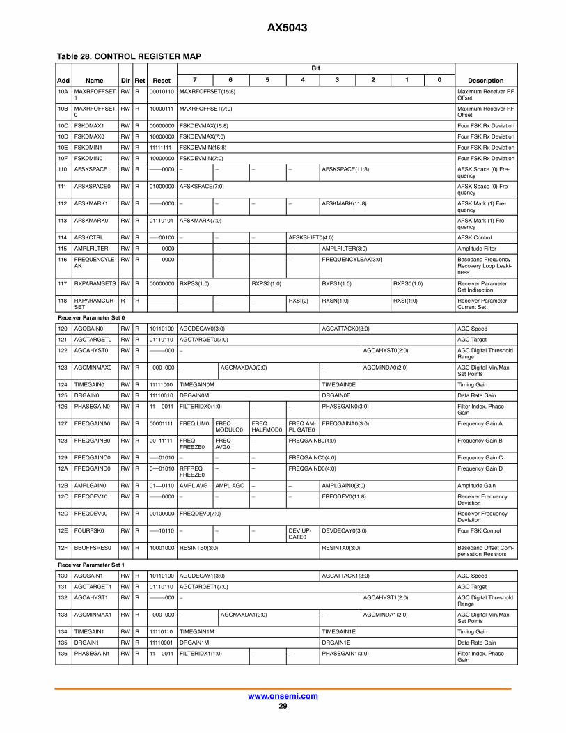
AX5043
www.onsemi.com29
Table 28. CONTROL REGISTER MAPBit
Add Description01234567ResetRetDirName
10A MAXRFOFFSET1
RW R 00010110 MAXRFOFFSET(15:8) Maximum Receiver RFOffset
10B MAXRFOFFSET0
RW R 10000111 MAXRFOFFSET(7:0) Maximum Receiver RFOffset
10C FSKDMAX1 RW R 00000000 FSKDEVMAX(15:8) Four FSK Rx Deviation
10D FSKDMAX0 RW R 10000000 FSKDEVMAX(7:0) Four FSK Rx Deviation
10E FSKDMIN1 RW R 11111111 FSKDEVMIN(15:8) Four FSK Rx Deviation
10F FSKDMIN0 RW R 10000000 FSKDEVMIN(7:0) Four FSK Rx Deviation
110 AFSKSPACE1 RW R ––––0000 – – – – AFSKSPACE(11:8) AFSK Space (0) Fre-quency
111 AFSKSPACE0 RW R 01000000 AFSKSPACE(7:0) AFSK Space (0) Fre-quency
112 AFSKMARK1 RW R ––––0000 – – – – AFSKMARK(11:8) AFSK Mark (1) Fre-quency
113 AFSKMARK0 RW R 01110101 AFSKMARK(7:0) AFSK Mark (1) Fre-quency
114 AFSKCTRL RW R –––00100 – – – AFSKSHIFT0(4:0) AFSK Control
115 AMPLFILTER RW R ––––0000 – – – – AMPLFILTER(3:0) Amplitude Filter
116 FREQUENCYLE-AK
RW R ––––0000 – – – – FREQUENCYLEAK[3:0] Baseband FrequencyRecovery Loop Leaki-ness
117 RXPARAMSETS RW R 00000000 RXPS3(1:0) RXPS2(1:0) RXPS1(1:0) RXPS0(1:0) Receiver ParameterSet Indirection
118 RXPARAMCUR-SET
R R –––––––– – – – RXSI(2) RXSN(1:0) RXSI(1:0) Receiver ParameterCurrent Set
Receiver Parameter Set 0
120 AGCGAIN0 RW R 10110100 AGCDECAY0(3:0) AGCATTACK0(3:0) AGC Speed
121 AGCTARGET0 RW R 01110110 AGCTARGET0(7:0) AGC Target
122 AGCAHYST0 RW R –––––000 − AGCAHYST0(2:0) AGC Digital ThresholdRange
123 AGCMINMAX0 RW R –000–000 − AGCMAXDA0(2:0) − AGCMINDA0(2:0) AGC Digital Min/MaxSet Points
124 TIMEGAIN0 RW R 11111000 TIMEGAIN0M TIMEGAIN0E Timing Gain
125 DRGAIN0 RW R 11110010 DRGAIN0M DRGAIN0E Data Rate Gain
126 PHASEGAIN0 RW R 11––0011 FILTERIDX0(1:0) – – PHASEGAIN0(3:0) Filter Index, PhaseGain
127 FREQGAINA0 RW R 00001111 FREQ LIM0 FREQMODULO0
FREQHALFMOD0
FREQ AM-PL GATE0
FREQGAINA0(3:0) Frequency Gain A
128 FREQGAINB0 RW R 00–11111 FREQFREEZE0
FREQAVG0
– FREQGAINB0(4:0) Frequency Gain B
129 FREQGAINC0 RW R –––01010 – – – FREQGAINC0(4:0) Frequency Gain C
12A FREQGAIND0 RW R 0––01010 RFFREQFREEZE0
– – FREQGAIND0(4:0) Frequency Gain D
12B AMPLGAIN0 RW R 01––0110 AMPL AVG AMPL AGC – – AMPLGAIN0(3:0) Amplitude Gain
12C FREQDEV10 RW R ––––0000 – – – – FREQDEV0(11:8) Receiver FrequencyDeviation
12D FREQDEV00 RW R 00100000 FREQDEV0(7:0) Receiver FrequencyDeviation
12E FOURFSK0 RW R –––10110 – – – DEV UP-DATE0
DEVDECAY0(3:0) Four FSK Control
12F BBOFFSRES0 RW R 10001000 RESINTB0(3:0) RESINTA0(3:0) Baseband Offset Com-pensation Resistors
Receiver Parameter Set 1
130 AGCGAIN1 RW R 10110100 AGCDECAY1(3:0) AGCATTACK1(3:0) AGC Speed
131 AGCTARGET1 RW R 01110110 AGCTARGET1(7:0) AGC Target
132 AGCAHYST1 RW R –––––000 − AGCAHYST1(2:0) AGC Digital ThresholdRange
133 AGCMINMAX1 RW R –000–000 − AGCMAXDA1(2:0) − AGCMINDA1(2:0) AGC Digital Min/MaxSet Points
134 TIMEGAIN1 RW R 11110110 TIMEGAIN1M TIMEGAIN1E Timing Gain
135 DRGAIN1 RW R 11110001 DRGAIN1M DRGAIN1E Data Rate Gain
136 PHASEGAIN1 RW R 11––0011 FILTERIDX1(1:0) – – PHASEGAIN1(3:0) Filter Index, PhaseGain
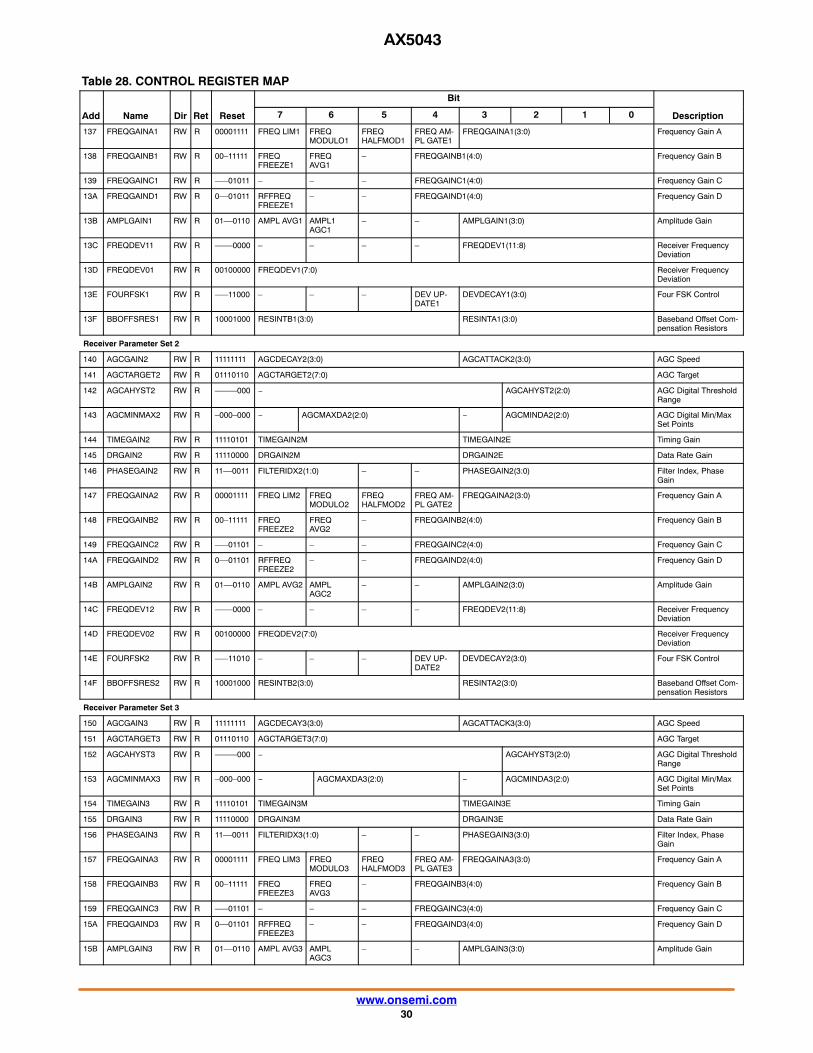
AX5043
www.onsemi.com30
Table 28. CONTROL REGISTER MAPBit
Add Description01234567ResetRetDirName
137 FREQGAINA1 RW R 00001111 FREQ LIM1 FREQMODULO1
FREQHALFMOD1
FREQ AM-PL GATE1
FREQGAINA1(3:0) Frequency Gain A
138 FREQGAINB1 RW R 00–11111 FREQFREEZE1
FREQAVG1
– FREQGAINB1(4:0) Frequency Gain B
139 FREQGAINC1 RW R –––01011 – – – FREQGAINC1(4:0) Frequency Gain C
13A FREQGAIND1 RW R 0––01011 RFFREQFREEZE1
– – FREQGAIND1(4:0) Frequency Gain D
13B AMPLGAIN1 RW R 01––0110 AMPL AVG1 AMPL1AGC1
– – AMPLGAIN1(3:0) Amplitude Gain
13C FREQDEV11 RW R ––––0000 – – – – FREQDEV1(11:8) Receiver FrequencyDeviation
13D FREQDEV01 RW R 00100000 FREQDEV1(7:0) Receiver FrequencyDeviation
13E FOURFSK1 RW R –––11000 – – – DEV UP-DATE1
DEVDECAY1(3:0) Four FSK Control
13F BBOFFSRES1 RW R 10001000 RESINTB1(3:0) RESINTA1(3:0) Baseband Offset Com-pensation Resistors
Receiver Parameter Set 2
140 AGCGAIN2 RW R 11111111 AGCDECAY2(3:0) AGCATTACK2(3:0) AGC Speed
141 AGCTARGET2 RW R 01110110 AGCTARGET2(7:0) AGC Target
142 AGCAHYST2 RW R –––––000 − AGCAHYST2(2:0) AGC Digital ThresholdRange
143 AGCMINMAX2 RW R –000–000 − AGCMAXDA2(2:0) − AGCMINDA2(2:0) AGC Digital Min/MaxSet Points
144 TIMEGAIN2 RW R 11110101 TIMEGAIN2M TIMEGAIN2E Timing Gain
145 DRGAIN2 RW R 11110000 DRGAIN2M DRGAIN2E Data Rate Gain
146 PHASEGAIN2 RW R 11––0011 FILTERIDX2(1:0) – – PHASEGAIN2(3:0) Filter Index, PhaseGain
147 FREQGAINA2 RW R 00001111 FREQ LIM2 FREQMODULO2
FREQHALFMOD2
FREQ AM-PL GATE2
FREQGAINA2(3:0) Frequency Gain A
148 FREQGAINB2 RW R 00–11111 FREQFREEZE2
FREQAVG2
– FREQGAINB2(4:0) Frequency Gain B
149 FREQGAINC2 RW R –––01101 – – – FREQGAINC2(4:0) Frequency Gain C
14A FREQGAIND2 RW R 0––01101 RFFREQFREEZE2
– – FREQGAIND2(4:0) Frequency Gain D
14B AMPLGAIN2 RW R 01––0110 AMPL AVG2 AMPLAGC2
– – AMPLGAIN2(3:0) Amplitude Gain
14C FREQDEV12 RW R ––––0000 – – – – FREQDEV2(11:8) Receiver FrequencyDeviation
14D FREQDEV02 RW R 00100000 FREQDEV2(7:0) Receiver FrequencyDeviation
14E FOURFSK2 RW R –––11010 – – – DEV UP-DATE2
DEVDECAY2(3:0) Four FSK Control
14F BBOFFSRES2 RW R 10001000 RESINTB2(3:0) RESINTA2(3:0) Baseband Offset Com-pensation Resistors
Receiver Parameter Set 3
150 AGCGAIN3 RW R 11111111 AGCDECAY3(3:0) AGCATTACK3(3:0) AGC Speed
151 AGCTARGET3 RW R 01110110 AGCTARGET3(7:0) AGC Target
152 AGCAHYST3 RW R –––––000 − AGCAHYST3(2:0) AGC Digital ThresholdRange
153 AGCMINMAX3 RW R –000–000 − AGCMAXDA3(2:0) − AGCMINDA3(2:0) AGC Digital Min/MaxSet Points
154 TIMEGAIN3 RW R 11110101 TIMEGAIN3M TIMEGAIN3E Timing Gain
155 DRGAIN3 RW R 11110000 DRGAIN3M DRGAIN3E Data Rate Gain
156 PHASEGAIN3 RW R 11––0011 FILTERIDX3(1:0) – – PHASEGAIN3(3:0) Filter Index, PhaseGain
157 FREQGAINA3 RW R 00001111 FREQ LIM3 FREQMODULO3
FREQHALFMOD3
FREQ AM-PL GATE3
FREQGAINA3(3:0) Frequency Gain A
158 FREQGAINB3 RW R 00–11111 FREQFREEZE3
FREQAVG3
– FREQGAINB3(4:0) Frequency Gain B
159 FREQGAINC3 RW R –––01101 – – – FREQGAINC3(4:0) Frequency Gain C
15A FREQGAIND3 RW R 0––01101 RFFREQFREEZE3
– – FREQGAIND3(4:0) Frequency Gain D
15B AMPLGAIN3 RW R 01––0110 AMPL AVG3 AMPLAGC3
– – AMPLGAIN3(3:0) Amplitude Gain

AX5043
www.onsemi.com31
Table 28. CONTROL REGISTER MAPBit
Add Description01234567ResetRetDirName
15C FREQDEV13 RW R ––––0000 – – – – FREQDEV3(11:8) Receiver FrequencyDeviation
15D FREQDEV03 RW R 00100000 FREQDEV3(7:0) Receiver FrequencyDeviation
15E FOURFSK3 RW R –––11010 – – – DEV UP-DATE3
DEVDECAY3(3:0) Four FSK Control
15F BBOFFSRES3 RW R 10001000 RESINTB3(3:0) RESINTA3(3:0) Baseband Offset Com-pensation Resistors
Transmitter Parameters
160 MODCFGF RW R ––––––00 – – – – – – FREQ SHAPE Modulator Configura-tion F
161 FSKDEV2 RW R 00000000 FSKDEV(23:16) FSK Frequency Devia-tion
162 FSKDEV1 RW R 00001010 FSKDEV(15:8) FSK Frequency Devia-tion
163 FSKDEV0 RW R 00111101 FSKDEV(7:0) FSK Frequency Devia-tion
164 MODCFGA RW R 0000–101 BROWNGATE
PTTLCKGATE
SLOW RAMP – AMPLSHAPE
TX SE TX DIFF Modulator Configura-tion A
165 TXRATE2 RW R 00000000 TXRATE(23:16) Transmitter Bitrate
166 TXRATE1 RW R 00101000 TXRATE(15:8) Transmitter Bitrate
167 TXRATE0 RW R 11110110 TXRATE(7:0) Transmitter Bitrate
168 TXPWRCOEFF-A1
RW R 00000000 TXPWRCOEFFA(15:8) Transmitter Predistor-tion Coefficient A
169 TXPWRCOEFF-A0
RW R 00000000 TXPWRCOEFFA(7:0) Transmitter Predistor-tion Coefficient A
16A TXPWRCOEFF-B1
RW R 00001111 TXPWRCOEFFB(15:8) Transmitter Predistor-tion Coefficient B
16B TXPWRCOEFF-B0
RW R 11111111 TXPWRCOEFFB(7:0) Transmitter Predistor-tion Coefficient B
16C TXPWRCOEFF-C1
RW R 00000000 TXPWRCOEFFC(15:8) Transmitter Predistor-tion Coefficient C
16D TXPWRCOEFF-C0
RW R 00000000 TXPWRCOEFFC(7:0) Transmitter Predistor-tion Coefficient C
16E TXPWRCOEFF-D1
RW R 00000000 TXPWRCOEFFD(15:8) Transmitter Predistor-tion Coefficient D
16F TXPWRCOEFF-D0
RW R 00000000 TXPWRCOEFFD(7:0) Transmitter Predistor-tion Coefficient D
170 TXPWRCOEFF-E1
RW R 00000000 TXPWRCOEFFE(15:8) Transmitter Predistor-tion Coefficient E
171 TXPWRCOEFF-E0
RW R 00000000 TXPWRCOEFFE(7:0) Transmitter Predistor-tion Coefficient E
PLL Parameters
180 PLLVCOI RW R 0–010010 VCOIE – VCOI(5:0) VCO Current
181 PLLVCOIR RW R –––––––– – – VCOIR(5:0) VCO Current Read-back
182 PLLLOCKDET RW R –––––011 LOCKDETDLYR – – – LOCK DETDLYM
LOCKDETDLY PLL Lock Detect Delay
183 PLLRNGCLK RW R –––––011 – – – – – PLLRNGCLK(2:0) PLL Ranging Clock
Crystal Oscillator
184 XTALCAP RW R 00000000 XTALCAP(7:0) Crystal Oscillator LoadCapacitance

AX5043
www.onsemi.com32
Table 28. CONTROL REGISTER MAPBit
Add Description01234567ResetRetDirName
Baseband
188 BBTUNE RW R –––01001 – – – BB TUNERUN
BBTUNE(3:0) Baseband Tuning
189 BBOFFSCAP RW R –111–111 – CAP INT B(2:0) – CAP INT A(2:0) Baseband Offset Com-pensation Capacitors
MAC Layer Parameters
Packet Format
200 PKTADDRCFG RW R 001–0000 MSB FIRST CRC SKIPFIRST
FEC SYNCDIS
– ADDR POS(3:0) Packet Address Config
201 PKTLENCFG RW R 00000000 LEN BITS(3:0 LEN POS(3:0) Packet Length Config
202 PKTLENOFFSE-T
RW R 00000000 LEN OFFSET(7:0) Packet Length Offset
203 PKTMAXLEN RW R 00000000 MAX LEN(7:0) Packet MaximumLength
204 PKTADDR3 RW R 00000000 ADDR(31:24) Packet Address 3
205 PKTADDR2 RW R 00000000 ADDR(23:16) Packet Address 2
206 PKTADDR1 RW R 00000000 ADDR(15:8) Packet Address 1
207 PKTADDR0 RW R 00000000 ADDR(7:0) Packet Address 0
208 PKTADDRMAS-K3
RW R 00000000 ADDRMASK(31:24) Packet Address Mask1
209 PKTADDRMAS-K2
RW R 00000000 ADDRMASK(23:16) Packet Address Mask0
20A PKTADDRMAS-K1
RW R 00000000 ADDRMASK(15:8) Packet Address Mask1
20B PKTADDRMAS-K0
RW R 00000000 ADDRMASK(7:0) Packet Address Mask0
Pattern Match
210 MATCH0PAT3 RW R 00000000 MATCH0PAT(31:24) Pattern Match Unit 0,Pattern
211 MATCH0PAT2 RW R 00000000 MATCH0PAT(23:16) Pattern Match Unit 0,Pattern
212 MATCH0PAT1 RW R 00000000 MATCH0PAT(15:8) Pattern Match Unit 0,Pattern
213 MATCH0PAT0 RW R 00000000 MATCH0PAT(7:0) Pattern Match Unit 0,Pattern
214 MATCH0LEN RW R 0––00000 MATCH0RAW
– – MATCH0LEN Pattern Match Unit 0,Pattern Length
215 MATCH0MIN RW R –––00000 – – – MATCH0MIN Pattern Match Unit 0,Minimum Match
216 MATCH0MAX RW R –––11111 – – – MATCH0MAX Pattern Match Unit 0,Maximum Match
218 MATCH1PAT1 RW R 00000000 MATCH1PAT(15:8) Pattern Match Unit 1,Pattern
219 MATCH1PAT0 RW R 00000000 MATCH1PAT(7:0) Pattern Match Unit 1,Pattern
21C MATCH1LEN RW R 0–––0000 MATCH1RAW
– – – MATCH1LEN Pattern Match Unit 1,Pattern Length
21D MATCH1MIN RW R ––––0000 – – – – MATCH1MIN Pattern Match Unit 1,Minimum Match
21E MATCH1MAX RW R ––––1111 – – – – MATCH1MAX Pattern Match Unit 1,Maximum Match
Packet Controller
220 TMGTXBOOST RW R 00110010 TMGTXBOOSTE TMGTXBOOSTM Transmit PLL BoostTime
221 TMGTXSETTLE RW R 00001010 TMGTXSETTLEE TMGTXSETTLEM Transmit PLL (postBoost) Settling Time
223 TMGRXBOOST RW R 00110010 TMGRXBOOSTE TMGRXBOOSTM Receive PLL BoostTime
224 TMGRXSETTLE RW R 00010100 TMGRXSETTLEE TMGRXSETTLEM Receive PLL (postBoost) Settling Time
225 TMGRXOFFSA-CQ
RW R 01110011 TMGRXOFFSACQE TMGRXOFFSACQM Receive Baseband DCOffset Acquisition Time
226 TMGRXCOARS-EAGC
RW R 00111001 TMGRXCOARSEAGCE TMGRXCOARSEAGCM Receive Coarse AGCTime
227 TMGRXAGC RW R 00000000 TMGRXAGCE TMGRXAGCM Receiver AGC SettlingTime
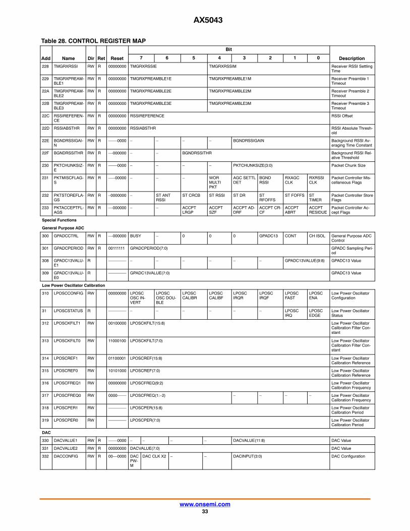
AX5043
www.onsemi.com33
Table 28. CONTROL REGISTER MAPBit
Add Description01234567ResetRetDirName
228 TMGRXRSSI RW R 00000000 TMGRXRSSIE TMGRXRSSIM Receiver RSSI SettlingTime
229 TMGRXPREAM-BLE1
RW R 00000000 TMGRXPREAMBLE1E TMGRXPREAMBLE1M Receiver Preamble 1Timeout
22A TMGRXPREAM-BLE2
RW R 00000000 TMGRXPREAMBLE2E TMGRXPREAMBLE2M Receiver Preamble 2Timeout
22B TMGRXPREAM-BLE3
RW R 00000000 TMGRXPREAMBLE3E TMGRXPREAMBLE3M Receiver Preamble 3Timeout
22C RSSIREFEREN-CE
RW R 00000000 RSSIREFERENCE RSSI Offset
22D RSSIABSTHR RW R 00000000 RSSIABSTHR RSSI Absolute Thresh-old
22E BGNDRSSIGAI-N
RW R ––––0000 – – – – BGNDRSSIGAIN Background RSSI Av-eraging Time Constant
22F BGNDRSSITHR RW R ––000000 – – BGNDRSSITHR Background RSSI Rel-ative Threshold
230 PKTCHUNKSIZ-E
RW R ––––0000 – – – – PKTCHUNKSIZE(3:0) Packet Chunk Size
231 PKTMISCFLAG-S
RW R –––00000 – – – WORMULTIPKT
AGC SETTLDET
BGNDRSSI
RXAGCCLK
RXRSSICLK
Packet Controller Mis-cellaneous Flags
232 PKTSTOREFLA-GS
RW R –0000000 – ST ANTRSSI
ST CRCB ST RSSI ST DR STRFOFFS
ST FOFFS STTIMER
Packet Controller StoreFlags
233 PKTACCEPTFL-AGS
RW R ––000000 – – ACCPTLRGP
ACCPTSZF
ACCPT AD-DRF
ACCPT CR-CF
ACCPTABRT
ACCPTRESIDUE
Packet Controller Ac-cept Flags
Special Functions
General Purpose ADC
300 GPADCCTRL RW R ––000000 BUSY – 0 0 0 GPADC13 CONT CH ISOL General Purpose ADCControl
301 GPADCPERIOD RW R 00111111 GPADCPERIOD(7:0) GPADC Sampling Peri-od
308 GPADC13VALU-E1
R –––––––– – – – – – – GPADC13VALUE(9:8) GPADC13 Value
309 GPADC13VALU-E0
R –––––––– GPADC13VALUE(7:0) GPADC13 Value
Low Power Oscillator Calibration
310 LPOSCCONFIG RW 00000000 LPOSCOSC IN-VERT
LPOSCOSC DOU-BLE
LPOSCCALIBR
LPOSCCALIBF
LPOSCIRQR
LPOSCIRQF
LPOSCFAST
LPOSCENA
Low Power OscillatorConfiguration
31 LPOSCSTATUS R –––––––– – – – – – – LPOSCIRQ
LPOSCEDGE
Low Power OscillatorStatus
312 LPOSCKFILT1 RW 00100000 LPOSCKFILT(15:8) Low Power OscillatorCalibration Filter Con-stant
313 LPOSCKFILT0 RW 11000100 LPOSCKFILT(7:0) Low Power OscillatorCalibration Filter Con-stant
314 LPOSCREF1 RW 01100001 LPOSCREF(15:8) Low Power OscillatorCalibration Reference
315 LPOSCREF0 RW 10101000 LPOSCREF(7:0) Low Power OscillatorCalibration Reference
316 LPOSCFREQ1 RW 00000000 LPOSCFREQ(9:2) Low Power OscillatorCalibration Frequency
317 LPOSCFREQ0 RW 0000–––– LPOSCFREQ(1:−2) – – – – Low Power OscillatorCalibration Frequency
318 LPOSCPER1 RW –––––––– LPOSCPER(15:8) Low Power OscillatorCalibration Period
319 LPOSCPER0 RW –––––––– LPOSCPER(7:0) Low Power OscillatorCalibration Period
DAC
330 DACVALUE1 RW R ––––0000 – – – – DACVALUE(11:8) DAC Value
331 DACVALUE2 RW R 00000000 DACVALUE(7:0) DAC Value
332 DACCONFIG RW R 00––0000 DACPW-M
DAC CLK X2 – – DACINPUT(3:0) DAC Configuration

AX5043
www.onsemi.com34
APPLICATION INFORMATION
Typical Application Diagrams
Match to 50 � for Differential Antenna Pins (868 / 915 / 433 / 169 MHz RX / TX Operation)
Figure 10. Structure of the Differential Antenna Interface for TX/RX Operation to 50 � Single−ended Equipment orAntenna
IC antennapins
LT1
LC1
LB1
CT1
CC1CM1
LT 2
LC2
CT2
CC2 CM2
CB2
LB2
CF
LF
CA CA
Optional filter stageto suppress TX
harmonics
50 � single−endedequipment or antenna
Table 29. TYPICAL COMPONENT VALUES
Frequency BandLC1,2[nH]
CC1,2[pF]
CT1,2[pF]
LT1,2[nH]
CM1[pF]
CM2[pF]
LB1,2[nH]
CB2[pF]
CF[pF]
optional
LF[nH]
optional
CA[pF]
optional
868 / 915 MHz 18 nc 2.7 18 6.2 3.6 12 2.7 nc 0 � nc
433 MHz 100 nc 4.3 43 11 5.6 27 5.1 nc 0 � nc
470 MHz 100 nc 3.9 33 4.7 nc 22 4.7 nc 0 � nc
169 MHz 150 10 10 120 12 nc 68 12 6.8 30 27

AX5043
www.onsemi.com35
Match to 50 � for Single−ended Antenna Pin(868 / 915 / 433 MHz TX Operation)
Figure 11. Structure of the Single−ended Antenna Interface for TX Operation to 50 � Single−ended Equipment orAntenna
IC AntennaPin LT
LC
CT
CC
CF1
LF1
CA1 CA2
50 � single−endedequipment or antenna
Table 30. TYPICAL COMPONENT VALUES
Frequency Band LC [nH] CC [pF] CT [pF] LT [nH] CF1 [pF] LF1 [nH] CA1 [pF] CA2 [pF]
868 / 915 MHz 18 nc 2.7 18 3.6 2.2 3.6 nc
433 MHz 100 nc 4.3 43 6.8 4.7 5.6 nc
Match to 50 � for Single−ended Antenna Pin (169 MHz TX Operation)
Figure 12. Structure of the Single−ended Antenna Interface for TX Operation to 50 � Single−ended Equipment orAntenna
IC AntennaPin LT
LC
CT
CC
CF1
LF1
CA1
50 � single−endedequipment or antenna
CA2
CF2
LF2
CA3
Table 31. TYPICAL COMPONENT VALUES
Frequency BandLC
[nH]CC[pF]
CT[pF]
LT[nH]
CF1[pF]
LF1[nH]
CF2[pF]
LF2[nH]
CA1[pF]
CA2[pF]
CA3[pF]
169 MHz 150 2.2 22 120 4.7 39 1.8 47 33 47 15

AX5043
www.onsemi.com36
Using a Dipole Antenna and the Internal TX/RX Switch
Figure 13. Typical Application Diagram with Dipole Antenna and Internal TX/RX Switch
VDD_ANA
GND
ANTP
ANTN
ANTP1
GND
VDD_ANA
CLK
16P
CLK
16N
GP
AD
C2
GP
AD
C1
NC
VD
D_I
O
NC
ANTSEL
PWRAMP
IRQ
NC
MOSI
MISO
CLK
FIL
T
L2 L1 DA
TA
SY
SC
LK
SE
L
DC
LK
AX5043
Mic
roco
ntro
ller

AX5043
www.onsemi.com37
Using a Single−ended Antenna and the Internal TX/RX Switch
Figure 14. Typical Application Diagram with Single−ended Antenna and Internal TX/RX Switch
VDD_ANA
GND
ANTP
ANTN
ANTP1
GND
VDD_ANA
CLK
16P
CLK
16N
GP
AD
C2
GP
AD
C1
NC
VD
D_I
O
NC
ANTSEL
PWRAMP
IRQ
NC
MOSI
MISO
CLK
FIL
T
L2 L1 DA
TA
SY
SC
LK
SE
L
DC
LK
AX504350 �
Mic
roco
ntro
ller

AX5043
www.onsemi.com38
Using an External High−power PA and an External TX/RX Switch
Figure 15. Typical Application Diagram with Single−ended Antenna, External PA and External Antenna Switch
VDD_ANA
GND
ANTP
ANTN
ANTP1
GND
VDD_ANA
CLK
16P
CLK
16N
GP
AD
C2
GP
AD
C1
NC
VD
D_I
O
NC
ANTSEL
PWRAMP
IRQ
NC
MOSI
MISO
CLK
FIL
T
L2 L1 DA
TA
SY
SC
LK
SE
L
DC
LK
AX5043
PA
TX/RX switch
50 �
Mic
roco
ntro
ller
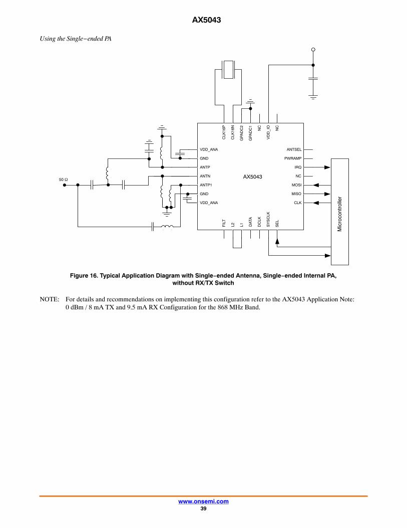
AX5043
www.onsemi.com39
Using the Single−ended PA
Figure 16. Typical Application Diagram with Single−ended Antenna, Single−ended Internal PA,without RX/TX Switch
VDD_ANA
GND
ANTP
ANTN
ANTP1
GND
VDD_ANA
CLK
16P
CLK
16N
GP
AD
C2
GP
AD
C1
NC
VD
D_I
O
NC
ANTSEL
PWRAMP
IRQ
NC
MOSI
MISO
CLK
FIL
T
L2 L1 DA
TA
SY
SC
LK
SE
L
DC
LK
AX504350 �
Mic
roco
ntro
ller
NOTE: For details and recommendations on implementing this configuration refer to the AX5043 Application Note:0 dBm / 8 mA TX and 9.5 mA RX Configuration for the 868 MHz Band.
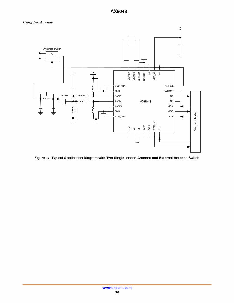
AX5043
www.onsemi.com40
Using Two Antenna
Figure 17. Typical Application Diagram with Two Single−ended Antenna and External Antenna Switch
VDD_ANA
GND
ANTP
ANTN
ANTP1
GND
VDD_ANA
CLK
16P
CLK
16N
GP
AD
C2
GP
AD
C1
NC
VD
D_I
O
NC
ANTSEL
PWRAMP
IRQ
NC
MOSI
MISO
CLK
FIL
T
L2 L1 DA
TA
SY
SC
LK
SE
L
DC
LK
AX5043
Antenna switch
Mic
roco
ntro
ller

AX5043
www.onsemi.com41
Using an External VCO Inductor
Figure 18. Typical Application Diagram with External VCO Inductor
VDD_ANA
GND
ANTP
ANTN
ANTP1
GND
VDD_ANA
CLK
16P
CLK
16N
GP
AD
C2
GP
AD
C1
NC
VD
D_I
O
NC
ANTSEL
PWRAMP
IRQ
NC
MOSI
MISO
CLK
FIL
T
L2 L1 DA
TA
SY
SC
LK
SE
L
DC
LK
AX5043
LVCO
Mic
roco
ntro
ller

AX5043
www.onsemi.com42
Using an External VCO
Figure 19. Typical Application Diagram with External VCO
VDD_ANA
GND
ANTP
ANTN
ANTP1
GND
VDD_ANA
CLK
16P
CLK
16N
GP
AD
C2
GP
AD
C1
NC
VD
D_I
O
NC
ANTSEL
PWRAMP
IRQ
NC
MOSI
MISO
CLK
FIL
T
L2 L1 GP
IO (
DA
TA)
SY
SC
LK
SE
L
DC
LK
AX5043
VC
TR
L
OU
TP
OU
TN
EN
VCO
Mic
roco
ntro
ller
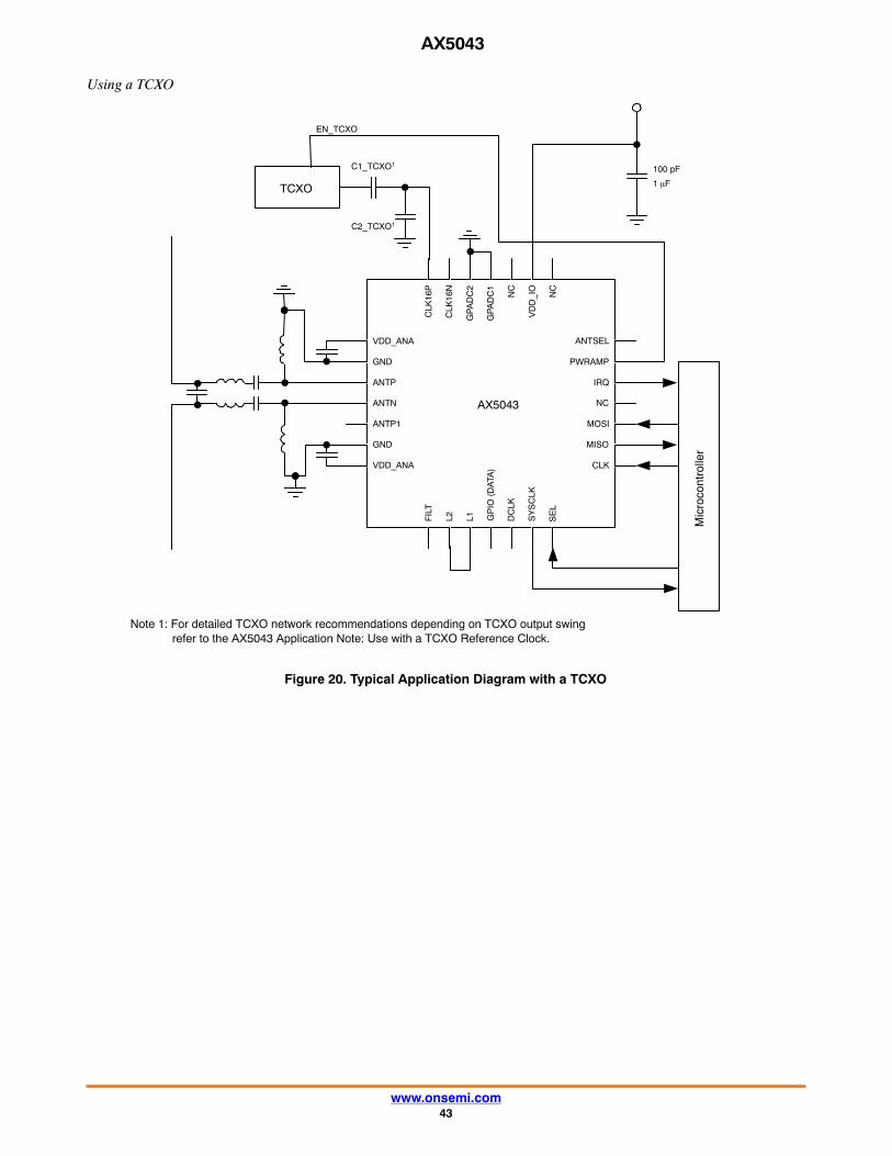
AX5043
www.onsemi.com43
Using a TCXO
Figure 20. Typical Application Diagram with a TCXO
VDD_ANA
GND
ANTP
ANTN
ANTP1
GND
VDD_ANA
CLK
16P
CLK
16N
GP
AD
C2
GP
AD
C1
NC
VD
D_I
O
NC
ANTSEL
PWRAMP
IRQ
NC
MOSI
MISO
CLK
FIL
T
L2 L1 GP
IO (
DA
TA)
SY
SC
LK
SE
L
DC
LK
AX5043
TCXO
C1_TCXO1
C2_TCXO1
EN_TCXO
100 pF
1 �F
Mic
roco
ntro
ller
Note 1: For detailed TCXO network recommendations depending on TCXO output swing refer to the AX5043 Application Note: Use with a TCXO Reference Clock.
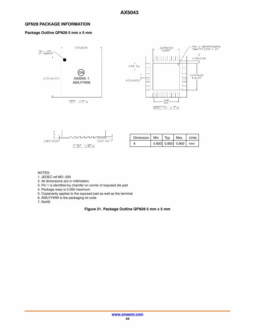
AX5043
www.onsemi.com44
QFN28 PACKAGE INFORMATION
Package Outline QFN28 5 mm x 5 mm
Figure 21. Package Outline QFN28 5 mm x 5 mm
NOTES:1. JEDEC ref MO−2202. All dimensions are in millimeters3. Pin 1 is identified by chamfer on corner of exposed die pad4. Package warp is 0.050 maximum5. Coplanarity applies to the exposed pad as well as the terminal6. AWLYYWW is the packaging lot code7. RoHS
Dimension Min Typ Max Units
A 0.800 0.850 0.900 mm
AX5043−1AWLYYWW
ON

AX5043
www.onsemi.com45
QFN28 Soldering Profile
Figure 22. QFN40 Soldering Profile
Preheat Reflow Cooling
TP
TL
TsMAX
TsMIN
ts
tL
tP
T25°C to Peak
Tem
pera
ture
Time
25°C
Table 32.
Profile Feature Pb−Free Process
Average Ramp−Up Rate 3°C/s max.
Preheat Preheat
Temperature Min TsMIN 150°C
Temperature Max TsMAX 200°C
Time (TsMIN to TsMAX) ts 60 – 180 sec
Time 25°C to Peak Temperature T25°C to Peak 8 min max.
Reflow Phase
Liquidus Temperature TL 217°C
Time over Liquidus Temperature tL 60 – 150 s
Peak Temperature tp 260°C
Time within 5°C of actual Peak Temperature Tp 20 – 40 s
Cooling Phase
Ramp−down rate 6°C/s max.
1. All temperatures refer to the top side of the package, measured on the the package body surface.

AX5043
www.onsemi.com46
QFN28 Recommended Pad Layout
1. PCB land and solder masking recommendationsare shown in Figure 23.
Figure 23. PCB Land and Solder Mask Recommendations
A = Clearance from PCB thermal pad to solder mask opening, 0.0635 mm minimumB = Clearance from edge of PCB thermal pad to PCB land, 0.2 mm minimumC = Clearance from PCB land edge to solder mask opening to be as tight as possible
to ensure that some solder mask remains between PCB pads.D = PCB land length = QFN solder pad length + 0.1 mmE = PCB land width = QFN solder pad width + 0.1 mm
2. Thermal vias should be used on the PCB thermalpad (middle ground pad) to improve thermalconductivity from the device to a copper groundplane area on the reverse side of the printed circuitboard. The number of vias depends on the packagethermal requirements, as determined by thermalsimulation or actual testing.
3. Increasing the number of vias through the printedcircuit board will improve the thermalconductivity to the reverse side ground plane andexternal heat sink. In general, adding more metalthrough the PC board under the IC will improveoperational heat transfer, but will require carefulattention to uniform heating of the board duringassembly.
Assembly Process
Stencil Design & Solder Paste Application1. Stainless steel stencils are recommended for solder
paste application.2. A stencil thickness of 0.125 – 0.150 mm
(5 – 6 mils) is recommended for screening.
3. For the PCB thermal pad, solder paste should beprinted on the PCB by designing a stencil with anarray of smaller openings that sum to 50% of theQFN exposed pad area. Solder paste should beapplied through an array of squares (or circles) asshown in Figure 24.
4. The aperture opening for the signal pads should bebetween 50−80% of the QFN pad area as shown inFigure 25.
5. Optionally, for better solder paste release, theaperture walls should be trapezoidal and thecorners rounded.
6. The fine pitch of the IC leads requires accuratealignment of the stencil and the printed circuitboard. The stencil and printed circuit assemblyshould be aligned to within + 1 mil prior toapplication of the solder paste.
7. No−clean flux is recommended since flux fromunderneath the thermal pad will be difficult toclean if water−soluble flux is used.
Figure 24. Solder Paste Application on Exposed Pad
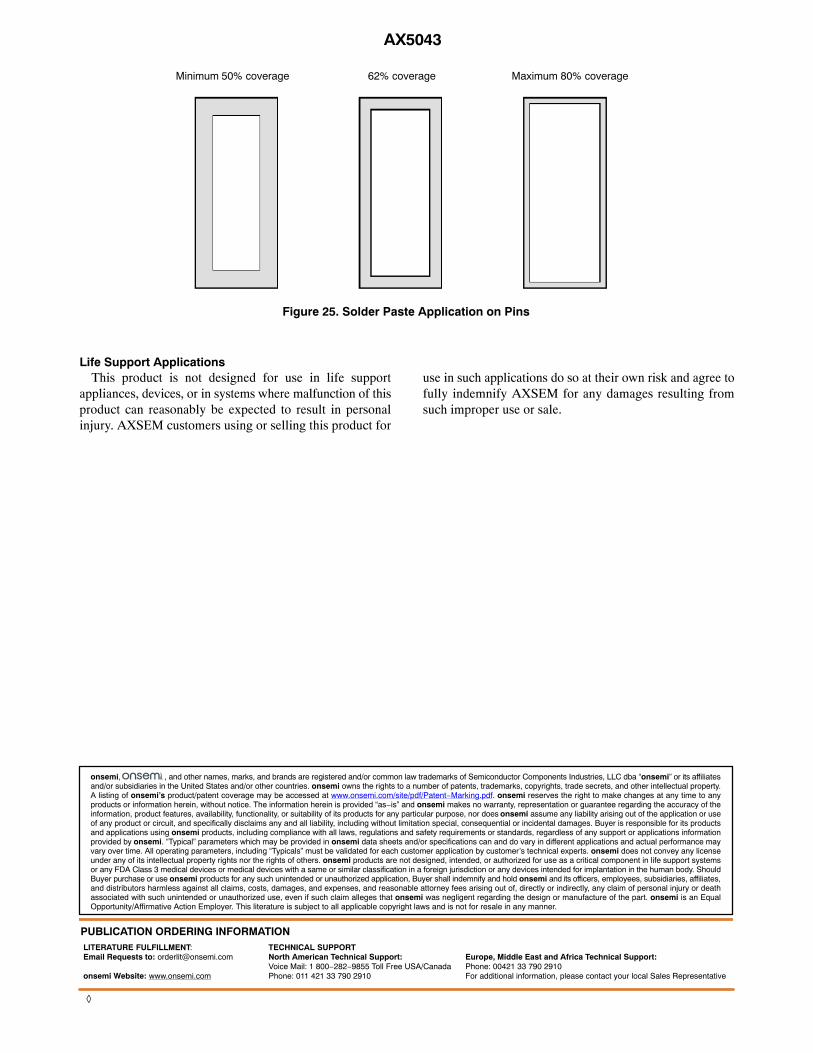
AX5043
www.onsemi.com47
Figure 25. Solder Paste Application on Pins
Minimum 50% coverage 62% coverage Maximum 80% coverage
Life Support ApplicationsThis product is not designed for use in life support
appliances, devices, or in systems where malfunction of thisproduct can reasonably be expected to result in personalinjury. AXSEM customers using or selling this product for
use in such applications do so at their own risk and agree tofully indemnify AXSEM for any damages resulting fromsuch improper use or sale.
onsemi, , and other names, marks, and brands are registered and/or common law trademarks of Semiconductor Components Industries, LLC dba “onsemi” or its affiliatesand/or subsidiaries in the United States and/or other countries. onsemi owns the rights to a number of patents, trademarks, copyrights, trade secrets, and other intellectual property.A listing of onsemi’s product/patent coverage may be accessed at www.onsemi.com/site/pdf/Patent−Marking.pdf. onsemi reserves the right to make changes at any time to anyproducts or information herein, without notice. The information herein is provided “as−is” and onsemi makes no warranty, representation or guarantee regarding the accuracy of theinformation, product features, availability, functionality, or suitability of its products for any particular purpose, nor does onsemi assume any liability arising out of the application or useof any product or circuit, and specifically disclaims any and all liability, including without limitation special, consequential or incidental damages. Buyer is responsible for its productsand applications using onsemi products, including compliance with all laws, regulations and safety requirements or standards, regardless of any support or applications informationprovided by onsemi. “Typical” parameters which may be provided in onsemi data sheets and/or specifications can and do vary in different applications and actual performance mayvary over time. All operating parameters, including “Typicals” must be validated for each customer application by customer’s technical experts. onsemi does not convey any licenseunder any of its intellectual property rights nor the rights of others. onsemi products are not designed, intended, or authorized for use as a critical component in life support systemsor any FDA Class 3 medical devices or medical devices with a same or similar classification in a foreign jurisdiction or any devices intended for implantation in the human body. ShouldBuyer purchase or use onsemi products for any such unintended or unauthorized application, Buyer shall indemnify and hold onsemi and its officers, employees, subsidiaries, affiliates,and distributors harmless against all claims, costs, damages, and expenses, and reasonable attorney fees arising out of, directly or indirectly, any claim of personal injury or deathassociated with such unintended or unauthorized use, even if such claim alleges that onsemi was negligent regarding the design or manufacture of the part. onsemi is an EqualOpportunity/Affirmative Action Employer. This literature is subject to all applicable copyright laws and is not for resale in any manner.
PUBLICATION ORDERING INFORMATIONTECHNICAL SUPPORTNorth American Technical Support:Voice Mail: 1 800−282−9855 Toll Free USA/CanadaPhone: 011 421 33 790 2910
LITERATURE FULFILLMENT:Email Requests to: [email protected]
onsemi Website: www.onsemi.com
Europe, Middle East and Africa Technical Support:Phone: 00421 33 790 2910For additional information, please contact your local Sales Representative
◊