Embed Size (px)
Citation preview
DATASHEET
AX5043
Advanced high performance ASK and FSK narrow-band transceiver for 27-1050 MHz range
Version 1.10
Version 1.10 Datasheet AX5043
2
Document Type Datasheet
Document Status
Document Version Version 1.10
Product AX5043
Table of Contents 3
Table of Contents
1. Overview..................................................................................................... 6
1.1. Features ..................................................................................................... 6
1.2. Applications................................................................................................. 7
2. Block Diagram............................................................................................. 8
3. Pin Function Descriptions ........................................................................... 9
3.1. Pinout Drawing .......................................................................................... 10
4. Specifications............................................................................................ 11
4.1. Absolute Maximum Ratings .......................................................................... 11
4.2. DC Characteristics ...................................................................................... 12
Supplies .................................................................................................... 12
Logic......................................................................................................... 14
4.3. AC Characteristics ...................................................................................... 15
Crystal Oscillator ........................................................................................ 15
Low-power Oscillator ................................................................................... 15
RF Frequency Generation Subsystem (Synthesizer) ......................................... 16
Transmitter................................................................................................ 19
Receiver .................................................................................................... 20
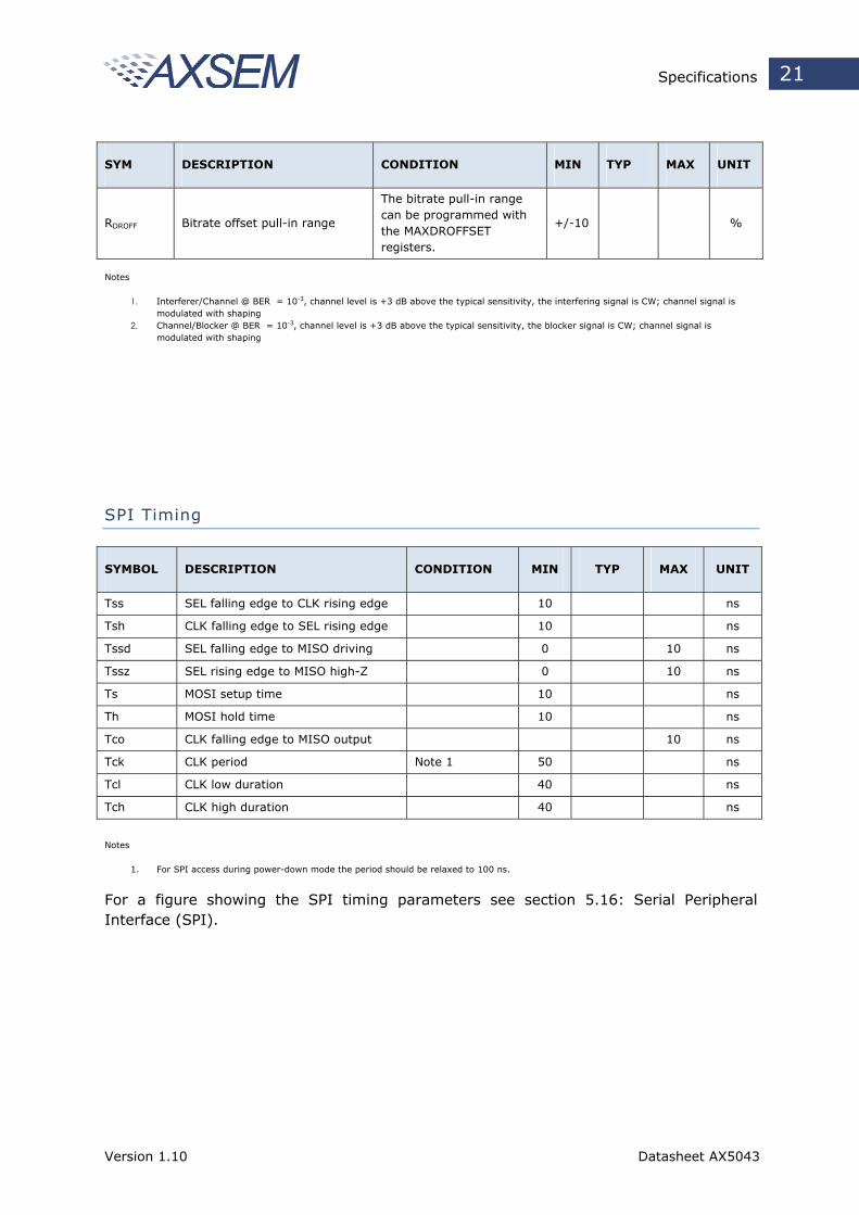
SPI Timing................................................................................................. 21
Wire Mode Interface Timing.......................................................................... 22
General Purpose ADC (GPADC) ..................................................................... 22
5. Circuit Description .................................................................................... 23
5.1. Voltage Regulators ..................................................................................... 24
5.2. Crystal Oscillator and TCXO Interface ............................................................ 25
5.3. Low Power Oscillator and Wake-on-Radio (WOR) Mode .................................... 25
5.4. GPIO Pins.................................................................................................. 26
5.5. SYSCLK Output .......................................................................................... 26
Version 1.10 Datasheet AX5043
Table of Contents 4
5.6. Power-on-reset (POR) ................................................................................. 27
5.7. RF Frequency Generation Subsystem............................................................. 27
VCO.......................................................................................................... 27
VCO Auto-Ranging ...................................................................................... 28
Loop Filter and Charge Pump........................................................................ 28
Registers ................................................................................................... 29
5.8. RF Input and Output Stage (ANTP/ANTN/ANTP1) ............................................ 30
LNA .......................................................................................................... 30
PA ............................................................................................................ 30
5.9. Digital IF Channel Filter and Demodulator ...................................................... 31
Registers ................................................................................................... 31
5.10. Encoder ................................................................................................ 32
5.11. Framing and FIFO................................................................................... 32
Packet Modes ............................................................................................. 33
RAW Modes................................................................................................ 34
5.12. RX AGC and RSSI................................................................................... 34
5.13. Modulator.............................................................................................. 35
5.14. Automatic Frequency Control (AFC)........................................................... 35
5.15. PWRMODE Register................................................................................. 36
5.16. Serial Peripheral Interface (SPI) ............................................................... 38
SPI Timing................................................................................................. 39
5.17. Wire Mode Interface ............................................................................... 40
Wire Mode Timing ....................................................................................... 40
5.18. General Purpose ADC (GPADC)................................................................. 41
5.19. Σ∆ DAC ................................................................................................. 41
6. Register Bank Description......................................................................... 42
6.1. Control Register Map................................................................................... 43
7. Application Information............................................................................ 55
7.1. Typical Application Diagrams........................................................................ 55
Version 1.10 Datasheet AX5043
Table of Contents 5
Match to 50 Ohm for differential antenna pins (868/915/433/169 MHz RX/TX operation) ................................................................................................. 55
Match to 50 Ohm for single-ended antenna pin (868/915/433 TX operation) ....... 56
Match to 50 Ohm for single-ended antenna pin (169 MHz TX operation) ............. 57
Using a Dipole Antenna and the internal TX/RX Switch ..................................... 58
Using a single-ended Antenna and the internal TX/RX Switch ............................ 59
Using an external high-power PA and an external TX/RX Switch ........................ 60
Using the single-ended PA............................................................................ 61
Using two Antenna...................................................................................... 62
Using an external VCO inductor .................................................................... 63
Using an external VCO................................................................................. 64
Using a TCXO............................................................................................. 65
8. QFN28 Package Information ..................................................................... 66
8.1. Package Outline QFN28 5 mm x 5 mm........................................................... 66
8.2. QFN28 Soldering Profile............................................................................... 67
8.3. QFN28 Recommended Pad Layout................................................................. 68
8.4. Assembly Process ....................................................................................... 68
Stencil Design & Solder Paste Application ....................................................... 68
9. Life Support Applications .......................................................................... 70
10. Contact Information.................................................................................. 71
Version 1.10 Datasheet AX5043
Overview 6
1. Overview
1.1. Features
Advanced multi-channel narrow-band single chip UHF transceiver (FSK/MSK/4-FSK/GFSK/GMSK/ ASK/AFSK/FM)
Low-Power
• RX 9.5 mA @ 868 MHz and 433 MHz 6.5 mA @ 169 MHz
• TX at 868 MHz 7.5 mA @ 0 dBm 16 mA @ 10 dBm 48 mA @ 16 dBm
• 50 nA deep sleep current
• 500 nA power-down current with low frequency duty cycle clock running
Extended supply voltage range
• 1.8 V - 3.6 V single supply
High sensitivity / High selectivity receiver
• Data rates from 0.1 kbps to 125 kbps
• Optional Forward Error Correction (FEC)
• Sensitivity without FEC –126 dBm @ 1.2 kbps, 868 MHz, FSK –116 dBm @ 10 kbps, 868 MHz, FSK –105 dBm @ 100 kbps, 868 MHz, FSK
• Sensitivity with FEC –137 dBm @ 0.1 kbps, 868 MHz, FSK –122 dBm @ 5 kbps, 868 MHz, FSK –111 dBm @ 50 kbps, 868 MHz, FSK
• High selectivity receiver with up to 47 dB adjacent channel rejection
• 0 dBm maximum input power
• > +/- 10% data-rate error tolerance
• Support for antenna diversity with external antenna switch
• Short preamble modes allow the receiver to work with as little as 16 preamble bits
Transmitter
• Data-rates from 0.1 kbps to 125 kbps
• High efficiency, high linearity integrated power amplifier
• Maximum output power 16 dBm @ 868 MHz 20 dBm @ 433 MHz 19 dBm @ 169 MHz
• Power level programmable in 0.5 dB steps
• GFSK shaping with BT=0.3 or BT=0.5
• Unrestricted power ramp shaping
Frequency Generation • Configurable for usage in 27 – 1050
MHz bands
• RF carrier frequency and FSK deviation programmable in 1 Hz steps
• Ultra fast settling RF frequency synthesizer for low-power consumption
• Fully integrated RF frequency synthesizer with VCO auto-ranging and band-width boost modes for fast locking
• Configurable for either fully integrated VCO, internal VCO with external inductor or fully external VCO
• Configurable for either fully integrated or external synthesizer loop filter for a large range of bandwidths
• Channel hopping up to 2000 hops/s
• Automatic frequency control (AFC)
Flexible antenna interface
• Integrated RX/TX switching with differential antenna pins
• Mode with differential RX pins and single-ended TX pin for usage with external PAs and for maximum PA efficiency at low output power
Wakeup-on-Radio
• 640 Hz or 10 kHz lowest power wake-up timer
• Wake-up time programmable between 98 µs and 102 s
Sophisticated radio controller • Antenna diversity and optional
external RX/TX switch control
• Fully automatic packet reception and transmission without micro-controller intervention
• Supports HDLC, Raw, Wireless M-Bus frames and arbitrary defined frames
• Automatic channel noise level tracking
Version 1.10 Datasheet AX5043
Table of Contents 7
• µs resolution timestamps for exact timing (e.g. for frequency hopping systems)
1.2. Applications
27 – 1050 MHz licensed and unlicensed radio systems.
• 256 Byte micro-programmable FIFO, optionally supports packet sizes > 256 Bytes
• 3 matching units for preamble byte, sync-word and address
• Internet of Things
• Ability to store RSSI, frequency offset and data-rate offset with the packet data
• Automatic meter reading (AMR)
• Security applications • Multiple receiver parameter sets allow
the use of more aggressive receiver parameters during preamble, dramatically shortening the required preamble length at no sensitivity degradation
• Building automation
• Wireless networks
• Messaging Paging
Advanced Crystal Oscillator • Compatible with: Wireless M-Bus,
POCSAG, FLEX, KNX, Sigfox, Z-Wave, enocean
• Fast start-up and lowest power steady-state XTAL oscillator for a wide range of crystals
• Integrated crystal tuning capacitors
• Possibility of applying an external clock reference (TCXO)
Miscellaneous features
• Few external components
• SPI microcontroller interface
• Extended AXSEM register set
• Fully integrated current/voltage references
• QFN28 5 mm x 5 mm package
• Internal power-on-reset
• Brown-out detection
• 10 bit 1MS/s General Purpose ADC (GPADC)
• Regulatory regimes: EN 300 220 V2.3.1 including the narrow-band 12.5 kHz, 20 kHz and 25 kHz definitions; EN 300 422; FCC Part 15.247; FCC Part 15.249; FCC Part 90 6.25 kHz, 12.5 kHz and 25 kHz
Version 1.10 Datasheet AX5043
Block Diagram 8
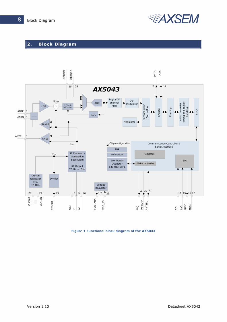
2. Block Diagram
Figure 1 Functional block diagram of the AX5043
AX5043
3ANTP
4ANTN
IF Filter & AGC PGAs
AGC
Crystal Oscillator
typ. 16 MHz
FOUT
RF Frequency Generation Subsystem
RF Output
70 MHz–1GHz
FXTAL
Communication Controller & Serial Interface
5
Divider
ADC
Digital IF channel
filter LNA
PA diff
De- modulator
Enco
der
Fram
ing
FIFO
Modulator
Mixer
28
CLK
16P
27
CLK
16N
Chip configuration
13
SYSCLK
SPI
Registers References
2319
IRQ
20
PWRAM
P AN
TSEL
21 14
SEL
15
CLK
16
MIS
O
MO
SI
17 10 9
FILT
L1
L2
8
Rad
io C
ontr
olle
r tim
ing a
nd p
ack
et
han
dlin
g
Forw
ard E
rror
Corr
ection
25 26
Wake on Radio Low Power Oscillator
640 Hz/10kHz
PA se
POR
VD
D_IO
1,7
VD
D_AN
A
Voltage Regulator
GPA
DC1
GPA
DC2
DCLK
DATA
11 12
ANTP1
Version 1.10 Datasheet AX5043
Pin Function Descriptions 9
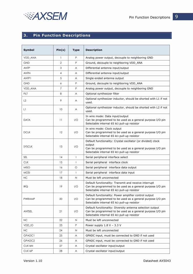
3. Pin Function Descriptions
Symbol Pin(s) Type Description
VDD_ANA 1 P Analog power output, decouple to neighboring GND
GND 2 P Ground, decouple to neighboring VDD_ANA
ANTP 3 A Differential antenna input/output
ANTN 4 A Differential antenna input/output
ANTP1 5 A Single-ended antenna output
GND 6 P Ground, decouple to neighboring VDD_ANA
VDD_ANA 7 P Analog power output, decouple to neighboring GND
FILT 8 A Optional synthesizer filter
L2 9 AOptional synthesizer inductor, should be shorted with L1 if not used.
L1 10 AOptional synthesizer inductor, should be shorted with L2 if not used.
DATA 11 I/OIn wire mode: Data input/output Can be programmed to be used as a general purpose I/O pin Selectable internal 65 kΩ pull-up resistor
DCLK 12 I/OIn wire mode: Clock output Can be programmed to be used as a general purpose I/O pin Selectable internal 65 kΩ pull-up resistor
SYSCLK 13 I/O
Default functionality: Crystal oscillator (or divided) clock output Can be programmed to be used as a general purpose I/O pin Selectable internal 65 kΩ pull-up resistor
SEL 14 I Serial peripheral interface select
CLK 15 I Serial peripheral interface clock
MISO 16 O Serial peripheral interface data output
MOSI 17 I Serial peripheral interface data input
NC 18 N Must be left unconnected
IRQ 19 I/ODefault functionality: Transmit and receive interrupt Can be programmed to be used as a general purpose I/O pin Selectable internal 65 kΩ pull-up resistor
PWRAMP 20 I/ODefault functionality: Power amplifier control output Can be programmed to be used as a general purpose I/O pin Selectable internal 65 kΩ pull-up resistor
ANTSEL 21 I/ODefault functionality: Diversity antenna selection output Can be programmed to be used as a general purpose I/O pin Selectable internal 65 kΩ pull-up resistor
NC 22 N Must be left unconnected
VDD_IO 23 P Power supply 1.8 V – 3.3 V
NC 24 N Must be left unconnected
GPADC1 25 A GPADC input, must be connected to GND if not used
GPADC2 26 A GPADC input, must be connected to GND if not used
CLK16N 27 A Crystal oscillator input/output
CLK16P 28 A Crystal oscillator input/output
Version 1.10 Datasheet AX5043
Pin Function Descriptions 10
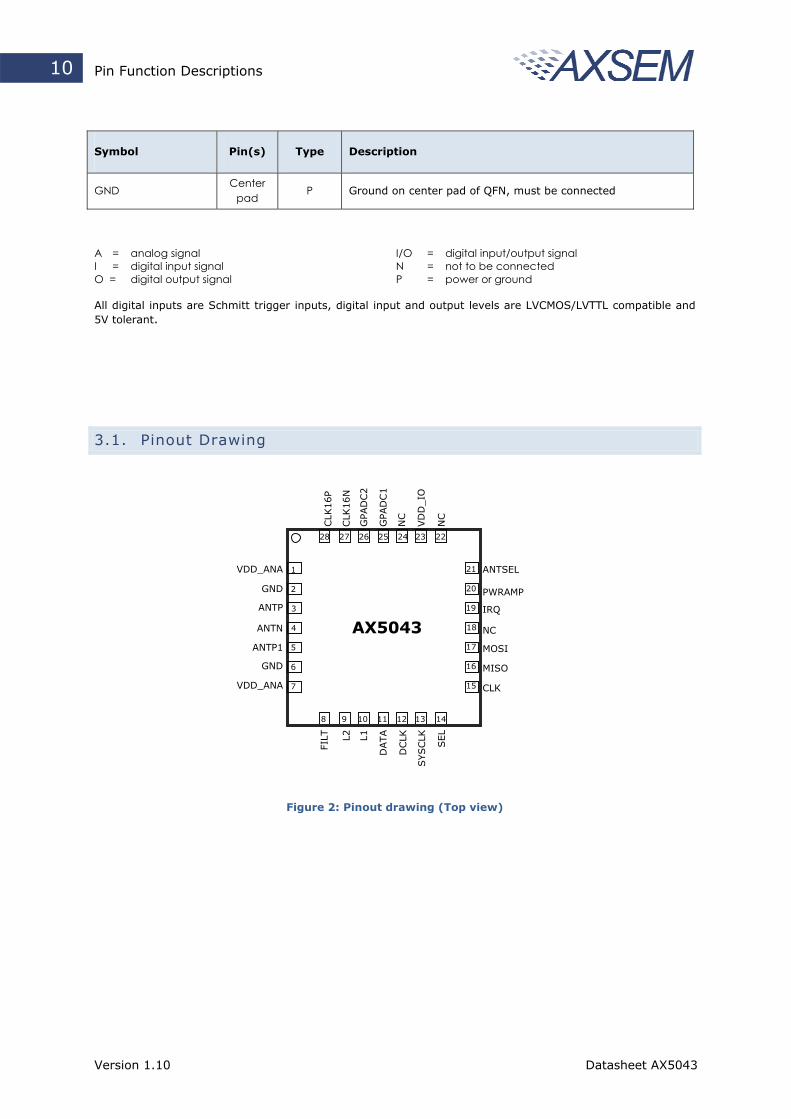
Symbol Pin(s) Type Description
GNDCenter
padP Ground on center pad of QFN, must be connected
A = analog signal I/O = digital input/output signal I = digital input signal N = not to be connected O = digital output signal P = power or ground All digital inputs are Schmitt trigger inputs, digital input and output levels are LVCMOS/LVTTL compatible and 5V tolerant.
3.1. Pinout Drawing
28 27 26 25 24 23 22
141311 12109 8
7
1
2
3
4
5
6
15
21
20
19
18
17
16
AX5043
NC
NC
GPAD
C1
VD
D_IO
GPAD
C2
CLK
16N
CLK
16P
SEL
SYSCLK
DCLK
DATAL1L2
FILT
CLK
IRQ
MOSI
NC
PWRAMP
MISO
ANTSEL
VDD_ANA
ANTP
ANTP1
ANTN
GND
GND
VDD_ANA
Figure 2: Pinout drawing (Top view)
Version 1.10
Datasheet AX5043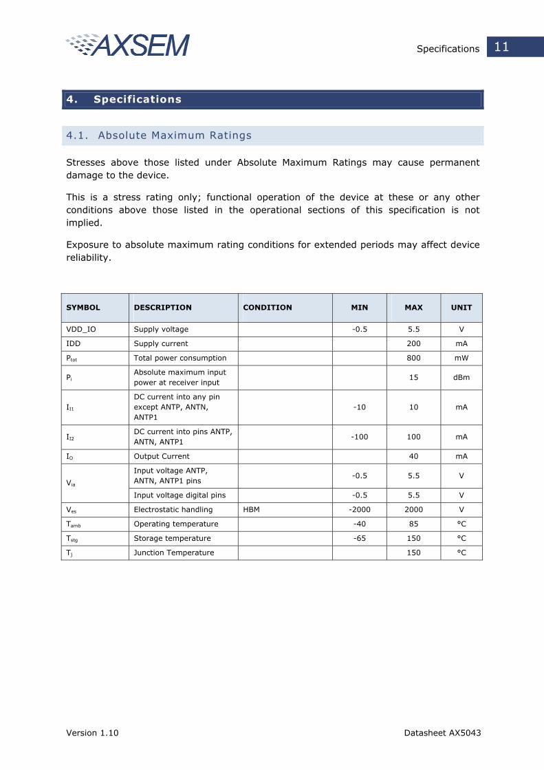
Specifications 11
4. Specifications
4.1. Absolute Maximum Ratings
Stresses above those listed under Absolute Maximum Ratings may cause permanent damage to the device.
This is a stress rating only; functional operation of the device at these or any other conditions above those listed in the operational sections of this specification is not implied.
Exposure to absolute maximum rating conditions for extended periods may affect device reliability.
SYMBOL DESCRIPTION CONDITION MIN MAX UNIT
VDD_IO Supply voltage -0.5 5.5 V
IDD Supply current 200 mA
Ptot Total power consumption 800 mW
PiAbsolute maximum input power at receiver input
15 dBm
II1
DC current into any pin except ANTP, ANTN, ANTP1
-10 10 mA
II2DC current into pins ANTP, ANTN, ANTP1
-100 100 mA
IO Output Current 40 mA
Input voltage ANTP, ANTN, ANTP1 pins
-0.5 5.5 V Via
Input voltage digital pins -0.5 5.5 V
Ves Electrostatic handling HBM -2000 2000 V
Tamb Operating temperature -40 85 °C
Tstg Storage temperature -65 150 °C
Tj Junction Temperature 150 °C
Version 1.10 Datasheet AX5043
Specifications 12
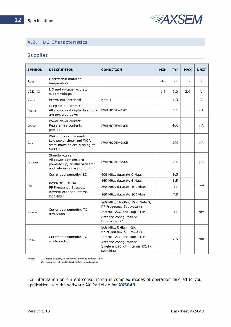
4.2. DC Characteristics
Supplies
SYMBOL DESCRIPTION CONDITION MIN TYP MAX UNIT
TAMBOperational ambient temperature
-40 27 85 °C
VDD_IO I/O and voltage regulator supply voltage
1.8 3.0 3.6 V
VBOUT Brown-out threshold Note 1 1.3 V
IDSLEEP
Deep-sleep current: All analog and digital functions are powered down
PWRMODE=0x01 50 nA
IPDOWN
Power-down current: Register file contents preserved
PWRMODE=0x00
400 nA
IWOR
Wakeup-on-radio mode: Low power timer and WOR state-machine are running at 640 Hz
PWRMODE=0x0B 500 nA
ISTANDBY
Standby-current: All power domains are powered up, crystal oscillator and references are running.
PWRMODE=0x05 230 µA
868 MHz, datarate 6 kbps 9.5
169 MHz, datarate 6 kbps 6.5
868 MHz, datarate 100 kbps 11 IRX
Current consumption RX PWRMODE=0x09 RF Frequency Subsystem: internal VCO and internal loop-filter 169 MHz, datarate 100 kbps 7.5
mA
ITX-DIFFCurrent consumption TX differential
868 MHz, 16 dBm, FSK, Note 2, RF Frequency Subsystem:
Internal VCO and loop-filter
Antenna configuration: Differential PA
48 mA
ITX-SECurrent consumption TX single ended
868 MHz, 0 dBm, FSK, RF Frequency Subsystem:
Internal VCO and loop-filter
Antenna configuration: Single ended PA, internal RX/TX switching
7.5 mA
Notes: 1. Digital circuitry is functional down to typically 1 V. 2. Measured with optimized matching networks.
For information on current consumption in complex modes of operation tailored to your application, see the software AX-RadioLab for AX5043.
Version 1.10 Datasheet AX5043
Specifications 13
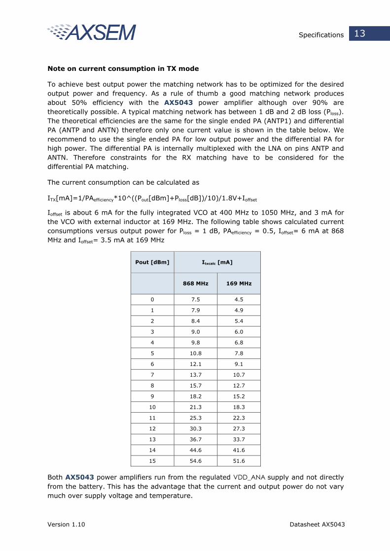
Note on current consumption in TX mode
To achieve best output power the matching network has to be optimized for the desired output power and frequency. As a rule of thumb a good matching network produces about 50% efficiency with the AX5043 power amplifier although over 90% are theoretically possible. A typical matching network has between 1 dB and 2 dB loss (Ploss). The theoretical efficiencies are the same for the single ended PA (ANTP1) and differential PA (ANTP and ANTN) therefore only one current value is shown in the table below. We recommend to use the single ended PA for low output power and the differential PA for high power. The differential PA is internally multiplexed with the LNA on pins ANTP and ANTN. Therefore constraints for the RX matching have to be considered for the differential PA matching.
The current consumption can be calculated as
ITX[mA]=1/PAefficiency*10^((Pout[dBm]+Ploss[dB])/10)/1.8V+Ioffset
Ioffset is about 6 mA for the fully integrated VCO at 400 MHz to 1050 MHz, and 3 mA for the VCO with external inductor at 169 MHz. The following table shows calculated current consumptions versus output power for Ploss = 1 dB, PAefficiency = 0.5, Ioffset= 6 mA at 868 MHz and Ioffset= 3.5 mA at 169 MHz
Pout [dBm] Itxcalc [mA]
868 MHz 169 MHz
0 7.5 4.5
1 7.9 4.9
2 8.4 5.4
3 9.0 6.0
4 9.8 6.8
5 10.8 7.8
6 12.1 9.1
7 13.7 10.7
8 15.7 12.7
9 18.2 15.2
10 21.3 18.3
11 25.3 22.3
12 30.3 27.3
13 36.7 33.7
14 44.6 41.6
15 54.6 51.6
Both AX5043 power amplifiers run from the regulated VDD_ANA supply and not directly from the battery. This has the advantage that the current and output power do not vary much over supply voltage and temperature.
Version 1.10 Datasheet AX5043
Specifications 14
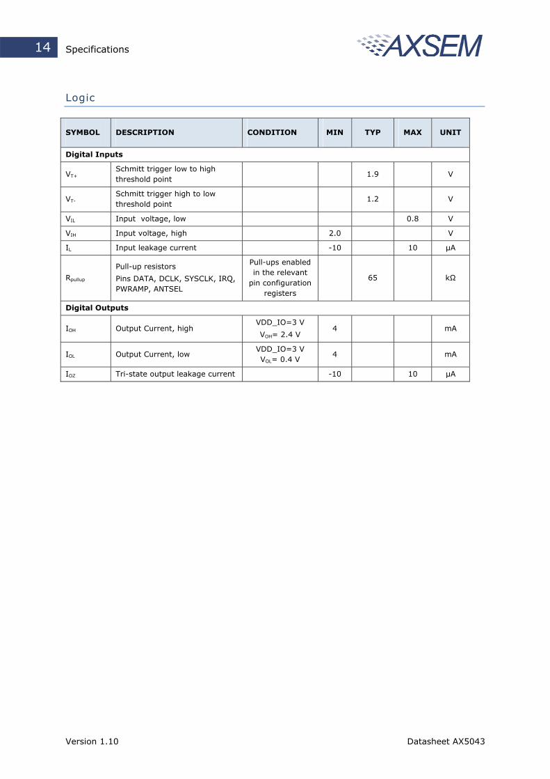
Logic
SYMBOL DESCRIPTION CONDITION MIN TYP MAX UNIT
Digital Inputs
VT+Schmitt trigger low to high threshold point
1.9 V
VT-Schmitt trigger high to low threshold point
1.2 V
VIL Input voltage, low 0.8 V
VIH Input voltage, high 2.0 V
IL Input leakage current -10 10 µA
Rpullup
Pull-up resistors
Pins DATA, DCLK, SYSCLK, IRQ, PWRAMP, ANTSEL
Pull-ups enabled in the relevant
pin configuration registers
65 kΩ
Digital Outputs
IOH Output Current, high VDD_IO=3 V
VOH= 2.4 V 4 mA
IOL Output Current, low VDD_IO=3 V VOL= 0.4 V
4 mA
IOZ Tri-state output leakage current -10 10 µA
Version 1.10 Datasheet AX5043
Specifications 15
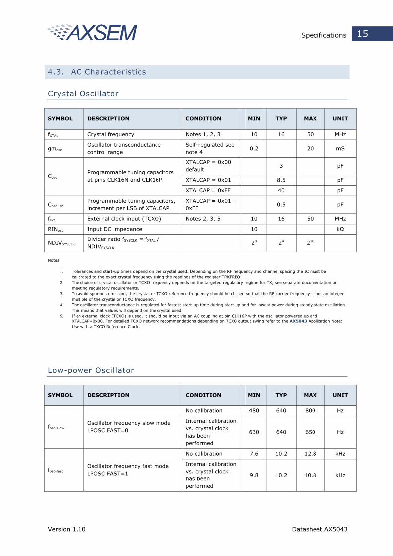
4.3. AC Characteristics
Crystal Oscillator
SYMBOL DESCRIPTION CONDITION MIN TYP MAX UNIT
fXTAL Crystal frequency Notes 1, 2, 3 10 16 50 MHz
gmoscOscillator transconductance control range
Self-regulated see note 4
0.2 20 mS
XTALCAP = 0x00 default
3 pF
XTALCAP = 0x01 8.5 pF Cosc
Programmable tuning capacitors at pins CLK16N and CLK16P
XTALCAP = 0xFF 40 pF
Cosc-lsbProgrammable tuning capacitors, increment per LSB of XTALCAP
XTALCAP = 0x01 – 0xFF
0.5 pF
fext External clock input (TCXO) Notes 2, 3, 5 10 16 50 MHz
RINosc Input DC impedance 10 kΩ
NDIVSYSCLKDivider ratio fSYSCLK = fXTAL / NDIVSYSCLK
20 24 210
Notes
1. Tolerances and start-up times depend on the crystal used. Depending on the RF frequency and channel spacing the IC must be calibrated to the exact crystal frequency using the readings of the register TRKFREQ
2. The choice of crystal oscillator or TCXO frequency depends on the targeted regulatory regime for TX, see separate documentation on meeting regulatory requirements.
3. To avoid spurious emission, the crystal or TCXO reference frequency should be chosen so that the RF carrier frequency is not an integer multiple of the crystal or TCXO frequency.
4. The oscillator transconductance is regulated for fastest start-up time during start-up and for lowest power during steady state oscillation. This means that values will depend on the crystal used.
5. If an external clock (TCXO) is used, it should be input via an AC coupling at pin CLK16P with the oscillator powered up and XTALCAP=0x00. For detailed TCXO network recommendations depending on TCXO output swing refer to the AX5043 Application Note: Use with a TXCO Reference Clock.
Low-power Oscillator
SYMBOL DESCRIPTION CONDITION MIN TYP MAX UNIT
No calibration 480 640 800 Hz
fosc-slowOscillator frequency slow mode LPOSC FAST=0
Internal calibration vs. crystal clock has been performed
630 640 650 Hz
No calibration 7.6 10.2 12.8 kHz
fosc-fastOscillator frequency fast mode LPOSC FAST=1
Internal calibration vs. crystal clock has been performed
9.8 10.2 10.8 kHz
Version 1.10 Datasheet AX5043
Specifications 16
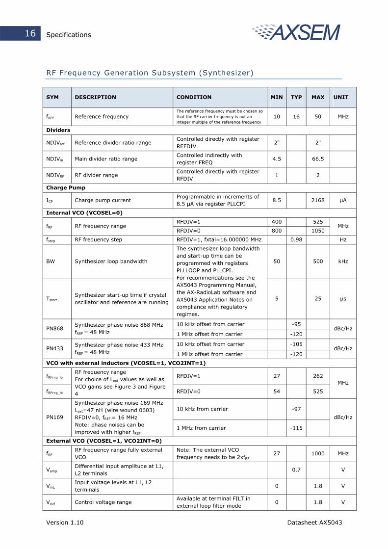
RF Frequency Generation Subsystem (Synthesizer)
SYM DESCRIPTION CONDITION MIN TYP MAX UNIT
fREF Reference frequency The reference frequency must be chosen so that the RF carrier frequency is not an integer multiple of the reference frequency
10 16 50 MHz
Dividers
NDIVref Reference divider ratio range Controlled directly with register REFDIV
20 23
NDIVm Main divider ratio range Controlled indirectly with register FREQ
4.5 66.5
NDIVRF RF divider range Controlled directly with register RFDIV
1 2
Charge Pump
ICP Charge pump current Programmable in increments of 8.5 µA via register PLLCPI
8.5 2168 µA
Internal VCO (VCOSEL=0)
RFDIV=1 400 525 fRF RF frequency range
RFDIV=0 800 1050 MHz
fstep RF frequency step RFDIV=1, fxtal=16.000000 MHz 0.98 Hz
BW Synthesizer loop bandwidth 50 500 kHz
TstartSynthesizer start-up time if crystal oscillator and reference are running
The synthesizer loop bandwidth and start-up time can be programmed with registers PLLLOOP and PLLCPI. For recommendations see the AX5043 Programming Manual, the AX-RadioLab software and AX5043 Application Notes on compliance with regulatory regimes.
5 25 µs
10 kHz offset from carrier -95 PN868
Synthesizer phase noise 868 MHz fREF = 48 MHz 1 MHz offset from carrier -120
dBc/Hz
10 kHz offset from carrier -105 PN433
Synthesizer phase noise 433 MHz fREF = 48 MHz 1 MHz offset from carrier -120
dBc/Hz
VCO with external inductors (VCOSEL=1, VCO2INT=1)
fRFrng_lo RFDIV=1 27 262
fRFrng_hi
RF frequency range For choice of Lext values as well as VCO gains see Figure 3 and Figure 4 RFDIV=0 54 525
MHz
10 kHz from carrier -97
PN169
Synthesizer phase noise 169 MHz Lext=47 nH (wire wound 0603) RFDIV=0, fREF = 16 MHz Note: phase noises can be improved with higher fREF
1 MHz from carrier -115
dBc/Hz
External VCO (VCOSEL=1, VCO2INT=0)
fRFRF frequency range fully external VCO
Note: The external VCO frequency needs to be 2xfRF
27 1000 MHz
VampDifferential input amplitude at L1, L2 terminals
0.7 V
VinLInput voltage levels at L1, L2 terminals
0 1.8 V
Vctrl Control voltage range Available at terminal FILT in external loop filter mode
0 1.8 V
Version 1.10 Datasheet AX5043
Specifications 17
Figure 3 VCO with external inductors: typical frequency vs Lext
Figure 4 VCO with external inductors: typical Kvco vs Lext
Version 1.10 Datasheet AX5043
Specifications 18
The following table shows the typical frequency ranges for frequency synthesis with external VCO inductor for different inductor values.
Lext [nH] Freq [MHz] Freq [MHz] PLL Range
RFDIV=0 RFDIV = 1
8.2 482 241 0
8.2 437 219 15
10 432 216 0
10 390 195 15
12 415 208 0
12 377 189 15
15 380 190 0
15 345 173 15
18 345 173 0
18 313 157 15
22 308 154 0
22 280 140 14
27 285 143 0
27 258 129 15
33 260 130 0
33 235 118 15
39 245 123 0
39 223 112 14
47 212 106 0
47 194 97 14
56 201 101 0
56 182 91 15
68 178 89 0
68 161 81 15
82 160 80 1
82 146 73 14
100 149 75 1
100 136 68 14
120 136 68 0
120 124 62 14
For tuning or changing of ranges a capacitor can be added in parallel to the inductor.
Version 1.10 Datasheet AX5043
Specifications 19
Transmitter
SYMBOL DESCRIPTION CONDITION MIN TYP MAX UNIT
SBR Signal bit rate 0.1 125 kbps
Transmitter power @ 868 MHz -10 16
Transmitter power @ 433 MHz -10 20 PTX
Transmitter power @ 169 MHz
Differential PA, 50 Ω single ended measurement at an SMA connector behind the matching network, Note 2 -10 19
dBm
PTXstepProgramming step size output power
Note 1 0.5 dB
dPTXtempTransmitter power variation vs. temperature
-40 °C to +85 °C Note 2
+/- 0.5 dB
dPTXVddTransmitter power variation vs. VDD_IO
1.8 V to 3.6 V Note 2
+/- 0.5 dB
868 MHz -44
Padj
Adjacent channel power
GFSK BT=0.5, 500 Hz deviation, 1.2kbps, 25 kHz channel spacing, 10 kHz channel BW
433 MHz
-51
dBc
PTX868-harm2 Emission @ 2nd harmonic -40
PTX868-harm3 Emission @ 3rd harmonic 868 MHz, Note 2
-60 dBc
PTX433-harm2 Emission @ 2nd harmonic -40
PTX433-harm3 Emission @ 3rd harmonic 433 MHz, Note 2
-40 dBc
Notes
1. max12 12PBTXPWRCOEFFPout •
−=
2. 50 Ω single ended measurements at an SMA connector behind the matching network. For recommended matching networks see section 7: Application Information
Version 1.10 Datasheet AX5043
Specifications 20
Receiver
SYM DESCRIPTION CONDITION MIN TYP MAX UNIT
SBR Signal bit rate 0.1 125 kbps
FSK, h = 0.5, 100 kbps -105
FSK, h = 0.5, 10 kbps -116 ISBER868
Input sensitivity at BER = 10-3
for 868 MHz operation, continuous data, without FEC
FSK, 500 Hz deviation, 1.2 kbps
-126
dBm
FSK, h = 0.5, 50 kbps -111
FSK, h = 0.5, 5 kbps -122 ISBER868FEC
Input sensitivity at BER = 10-3
for 868 MHz operation, continuous data, with FEC
FSK, 500 Hz deviation, 0.1 kbps
-137
dBm
FSK, h = 0.5, 100 kbps -103
FSK, h = 0.5, 10 kbps -115 ISPER868
Input sensitivity at PER = 1% for 868 MHz operation, 144 bit packet data, without FEC FSK, 1.2 kbps -125
dBm
ISWOR868
Input sensitivity at PER = 1% for 868 MHz operation, 144 bit packet data, WOR-mode, without FEC
FSK, h = 0.5, 100 kbps -102 dBm
IL Maximum input level 0 dBm
CP1dBInput referred compression point
2 tones separated by 100 kHz
-35 dBm
RSSIR RSSI control range FSK, 500 Hz deviation, 1.2 kbps
-126 -46 dB
RSSIS1 RSSI step size Before digital channel filter; calculated from register AGCCOUNTER
0.625 dB
RSSIS2 RSSI step size
Behind digital channel filter; calculated from registers AGCCOUNTER, TRKAMPL
0.1 dB
RSSIS3 RSSI step size Behind digital channel filter; reading register RSSI
1 dB
25 kHz channels Note 1
45
SEL868 Adjacent channel suppression 100 kHz channels Note 1
47
dB
BLK868 Blocking at +/- 10 MHz offset FSK 4.8 kbps Note 2
78 dB
RAFC AFC pull-in range
The AFC pull-in range can be programmed with the MAXRFOFFSET registers.
The AFC response time can be programmed with the FREQGAIND register.
+/-15 %
Version 1.10 Datasheet AX5043
Specifications 21
SYM DESCRIPTION CONDITION MIN TYP MAX UNIT
RDROFF Bitrate offset pull-in range
The bitrate pull-in range can be programmed with the MAXDROFFSET registers.
+/-10 %
Notes
1. Interferer/Channel @ BER = 10-3, channel level is +3 dB above the typical sensitivity, the interfering signal is CW; channel signal is modulated with shaping
2. Channel/Blocker @ BER = 10-3, channel level is +3 dB above the typical sensitivity, the blocker signal is CW; channel signal is modulated with shaping
SPI Timing
SYMBOL DESCRIPTION CONDITION MIN TYP MAX UNIT
Tss SEL falling edge to CLK rising edge 10 ns
Tsh CLK falling edge to SEL rising edge 10 ns
Tssd SEL falling edge to MISO driving 0 10 ns
Tssz SEL rising edge to MISO high-Z 0 10 ns
Ts MOSI setup time 10 ns
Th MOSI hold time 10 ns
Tco CLK falling edge to MISO output 10 ns
Tck CLK period Note 1 50 ns
Tcl CLK low duration 40 ns
Tch CLK high duration 40 ns
Notes
1. For SPI access during power-down mode the period should be relaxed to 100 ns.
For a figure showing the SPI timing parameters see section 5.16: Serial Peripheral Interface (SPI).
Version 1.10 Datasheet AX5043
Specifications 22
Wire Mode Interface Timing
SYMBOL DESCRIPTION CONDITION MIN TYP MAX UNIT
Tdck DCLK period Depends on bit rate programming
1.6 10000 µs
Tdcl DCLK low duration 25 75 %
Tdch DCLK high duration 25 75 %
Tds DATA setup time relative to active DCLK edge
10 ns
Tdh DATA hold time relative to active DCLK edge
10 ns
Tdco DATA output change relative to active DCLK edge
10 ns
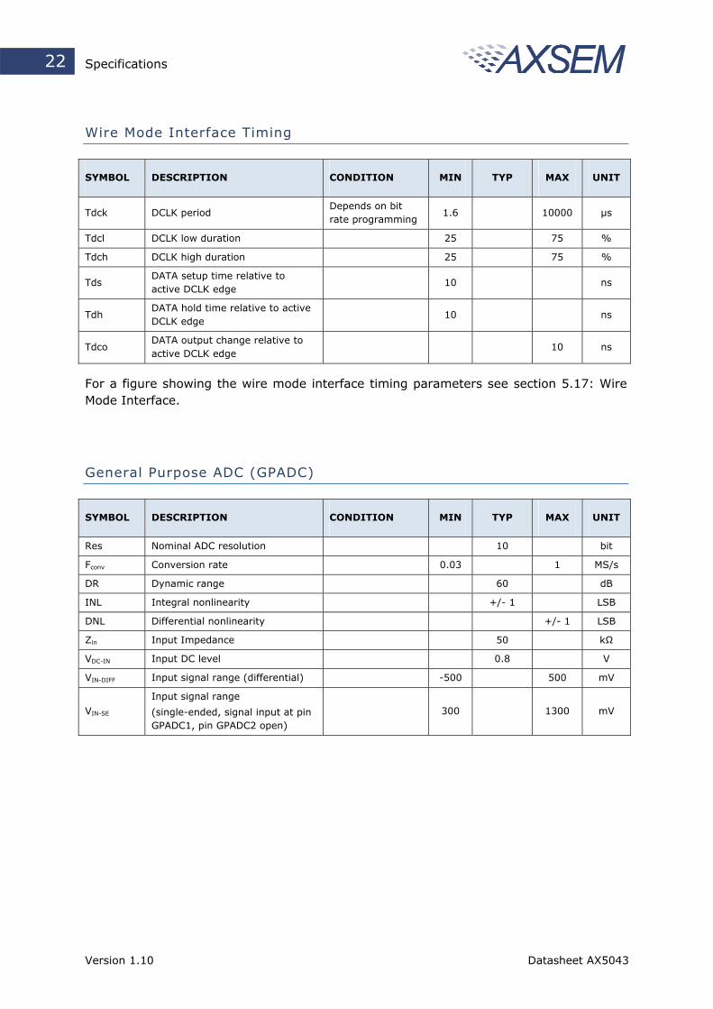
For a figure showing the wire mode interface timing parameters see section 5.17: Wire Mode Interface.
General Purpose ADC (GPADC)
SYMBOL DESCRIPTION CONDITION MIN TYP MAX UNIT
Res Nominal ADC resolution 10 bit
Fconv Conversion rate 0.03 1 MS/s
DR Dynamic range 60 dB
INL Integral nonlinearity +/- 1 LSB
DNL Differential nonlinearity +/- 1 LSB
Zin Input Impedance 50 kΩ
VDC-IN Input DC level 0.8 V
VIN-DIFF Input signal range (differential) -500 500 mV
VIN-SE
Input signal range
(single-ended, signal input at pin GPADC1, pin GPADC2 open)
300 1300 mV
Version 1.10 Datasheet AX5043
Circuit Description 23
5. Circuit Description
The AX5043 is a true single chip ultra-low power narrow-band CMOS transceiver for use in licensed and unlicensed bands from 27 and 1050 MHz. The on-chip transceiver consists of a fully integrated RF front-end with modulator, and demodulator. Base band data processing is implemented in an advanced and flexible communication controller that enables user friendly communication via the SPI interface.
AX5043 can be operated from a 1.8 V to 3.6 V power supply over a temperature range of -40oC to 85oC. It consumes 7 - 48 mA for transmitting at 868 MHz carrier frequency, 4 – 51 mA for transmitting at 169 MHz depending on the output power. In receive operation AX5043 consumes 9 - 11 mA at 868 MHz carrier frequency and 6.5 - 8.5 mA at 169 MHz.
The AX5043 features make it an ideal interface for integration into various battery powered solutions such as ticketing or as transceiver for telemetric applications e.g. in sensors. As primary application, the transceiver is intended for UHF radio equipment in accordance with the European Telecommunication Standard Institute (ETSI) specification EN 300 220-1 and the US Federal Communications Commission (FCC) standard Title 47 CFR Part 15 as well as Part 90. AX5043 is compliant with the respective narrow-band regulations. Additionally AX5043 is suited for systems targeting compliance with Wireless M-Bus standard EN 13757-4:2005. Wireless M-Bus frame support (S, T, R) is built-in.
AX5043 supports any data rate from 0.1 kbps to 125 kbps for FSK, 4-FSK, GFSK, GMSK, MSK and ASK. To achieve optimum performance for specific data rates and modulation schemes several register settings to configure the AX5043 are necessary, for details see the AXSEM RadioLab Software which calculates the necessary register settings and the AX5043 Programming Manual.
The AX5043 can be operated in two fundamentally different modes.
In frame mode data is sent and received via the SPI port in frames. Pre- and post-ambles as well as checksums can be generated automatically. Interrupts control the data flow between a micro-controller and the AX5043.
In wire mode the IC behaves as an extension of any wire. The internal communication controller is disabled and the modem data is directly available on a dedicated pin (DATA). The bit clock is also output on a dedicated pin (DCLK). In this mode the user can connect the data pin to any port of a micro-controller or to a UART, but has to control coding, checksums, pre and post ambles. The user can choose between synchronous and asynchronous wire mode, asynchronous wire mode performs RS232 start bit recognition and re-synchronization for transmit.
Both modes can be used both for transmit and receive. In both cases the AX5043 behaves as a SPI slave interface. Configuration of the AX5043 is always done via the SPI interface.
The receiver and the transmitter support multi-channel operation for all data rates and modulation schemes.
Version 1.10 Datasheet AX5043
Circuit Description 24
5.1. Voltage Regulators
The AX5043 uses an on-chip voltage regulator system to create stable supply voltages for the internal circuitry from the primary supply VDD_IO. The I/O level of the digital pins is VDD_IO.
Pins VDD_ANA are supplied for external decoupling of the power supply used for the on-chip PA.
The voltage regulator system must be set into the appropriate state before receive or transmit operations can be initiated. This is handled automatically when programming the device modes via the PWRMODE register.
Register POWSTAT contains status bits that can be read to check if the regulated voltages are ready (bit SVIO) or if VDD_IO has dropped below the brown-out level of 1.3V (bit SSUM).
In power-down mode the core supply voltages for digital and analog functions are switched off to minimize leakage power. Most register contents are preserved but access to the FIFO is not possible and FIFO contents are lost. SPI access to registers is possible, but at lower speed.
In deep-sleep mode all supply voltages are switched off. All digital and analog functions are disabled. All register contents are lost. To leave deep-sleep mode the pin SEL has to be pulled low. This will initiate startup and reset of the AX5043. Then the MISO line should be polled, as it will be held low during initialization and will rise to high at the end of the initialization, when the chip becomes ready for operation.
Version 1.10 Datasheet AX5043
Circuit Description 25
5.2. Crystal Oscillator and TCXO Interface
The AX5043 is normally operated with an external TCXO, which is required by most narrow-band regulation with a tolerance of 0.5 ppm to 1.5 ppm depending on the regulation. The on-chip crystal oscillator allows the use of an inexpensive quartz crystal as the RF generation subsystem’s timing reference when possible from a regulatory point of view.
A wide range of reference frequencies can be handled by the crystal oscillator circuit. As the reference frequency impacts both the spectral performance of the transmitter as well as the current consumption of the receiver, the choice of reference frequency should be made according to the regulatory regime targeted by the application. For guide-lines see the separate Application Notes for usage of AX5043 in compliance with various regulatory regimes.
The crystal or TCXO reference frequency should be chosen so that the RF carrier frequency is not an integer multiple of the crystal or TCXO frequency.
The oscillator circuit is enabled by programming the PWRMODE register. At power-up it is enabled.
To adjust the circuit’s characteristics to the quartz crystal being used, without using additional external components, the tuning capacitance of the crystal oscillator can be programmed. The transconductance of the oscillator is automatically regulated, to allow for fastest start-up times together with lowest power operation during steady-state oscillation.
The integrated programmable tuning capacitor bank makes it possible to connect the oscillator directly to pins CLK16N and CLK16P without the need for external capacitors. It is programmed using bits XTALCAP[5:0] in register XTALCAP.
To synchronize the receiver frequency to a carrier signal, the oscillator frequency could be tuned using the capacitor bank however, the recommended method to implement frequency synchronization is to make use of the high resolution RF frequency generation sub-system together with the Automatic Frequency Control, both are described further down.
Alternatively a single ended reference (TXCO, CXO) may be used. For detailed TCXO network recommendations depending on TCXO output swing refer to the AX5043 Application Note: Use with a TXCO Reference Clock.
5.3. Low Power Oscillator and Wake-on-Radio (WOR) Mode
The AX5043 features an internal lowest power fully integrated oscillator. In default mode the frequency of oscillation is 640 Hz +/- 1.5%, in fast mode it is 10.2 kHz +/- 1.5%. These accuracies are reached after the internal hardware has been used to calibrate the low power oscillator versus the RF reference clock. This procedure can be run in the background during transmit or receive operations.
The low power oscillator makes a WOR mode with a power consumption of 500nA possible.
Version 1.10 Datasheet AX5043
Circuit Description 26
If Wake-on-Radio Mode is enabled, the receiver wakes up periodically at a user selectable interval, and checks for a radio signal on the selected channel. If no signal is detected, the receiver shuts down again. If a radio signal is detected, and a valid packet is received, the micro-controller is alerted by asserting an interrupt.
The AX5043 can thus autonomously poll for radio signals, while the micro-controller can stay powered down, and only wakes up once a valid packet is received. This allows for very low average receiver power, at the expense of longer preambles at the transmitter.
5.4. GPIO Pins
Pins DATA, DCLK, SYSCLK, IRQ, ANTSEL , PWRAMP can be used as general purpose I/O pins by programming pin configuration registers PINFUNCSYSCLK, PINFUNCDCLK, PINFUNCDATA, PINFUNCIRQ, PINFUCNANTSEL, PINFUNCPWRAMP. Pin input values can be read via register PINSTATE. Pull-ups are disabled if output data is programmed to the GPIO pin.
65 kΩ
VDD_IO
VDD_IO
output data
input data
enable weak pull-up
enable output
Figure 5 GPIO pin
5.5. SYSCLK Output
The SYSCLK pin outputs either the reference clock signal divided by a programmable power of two or the low power oscillator clock. Division ratios from 1 to 1024 are possible. For divider ratios > 1 the duty cycle is 50%. Bits SYSCLK[4:0] in the PINFUNCSYSCLK register set the divider ratio. The SYSCLK output can be disabled.
After power-up SYSCLK outputs 1/16 of the crystal oscillator clock, making it possible to use this clock to boot a micro-controller.
Version 1.10 Datasheet AX5043
Circuit Description 27
5.6. Power-on-reset (POR)
AX5043 has an integrated power-on-reset block. No external POR circuit is required.
After POR the AX5043 can be reset by first setting the SPI SEL pin to high for at least 100 ns, then setting followed by resetting the bit RST in the PWRMODE register.
After POR or reset all registers are set to their default values.
5.7. RF Frequency Generation Subsystem
The RF frequency generation subsystem consists of a fully integrated synthesizer, which multiplies the reference frequency from the crystal oscillator to get the desired RF frequency. The advanced architecture of the synthesizer enables frequency resolutions of 1 Hz, as well as fast settling times of 5 – 50 µs depending on the settings (see section 4.3: AC Characteristics). Fast settling times mean fast start-up and fast RX/TX switching, which enables low-power system design.
For receive operation the RF frequency is fed to the mixer, for transmit operation to the power-amplifier.
The frequency must be programmed to the desired carrier frequency.
The synthesizer loop bandwidth can be programmed, this serves three purposes:
1. Start-up time optimization, start-up is faster for higher synthesizer loop bandwidths
2. TX spectrum optimization, phase-noise at 300 kHz to 1 MHz distance from the carrier improves with lower synthesizer loop bandwidths
3. Adaptation of the bandwidth to the data-rate. For transmission of FSK and MSK it is required that the synthesizer bandwidth must be in the order of the data-rate.
VCO
An on-chip VCO converts the control voltage generated by the charge pump and loop filter into an output frequency. This frequency is used for transmit as well as for receive operation. The frequency can be programmed in 1 Hz steps in the FREQ registers. For operation in the 433 MHz band, the RFDIV bit in the PLLVCODIV register must be programmed.
The fully integrated VCO allows to operate the device in the frequency ranges 800 – 1050 MHz and 400 – 525 MHz.
The carrier frequency range can be extended to 54 – 525 MHz and 27 – 262 MHz by using an appropriate external inductor between device pins L1 and L2. The bit VCO2INT in the PLLVCODIV register must be set high to enter this mode.
Version 1.10 Datasheet AX5043
Circuit Description 28
It is also possible to use a fully external VCO by setting bits VCO2INT=0 and VCOSEL=1 in the PLLVCODIV register. A differential input at a frequency of double the desired RF frequency must be input at device pins L1 and L2. The control voltage for the VCO can be output at device pin FILT when using external filter mode. The voltage range of this output pin is 0 – 1.8 V. This mode of operation is recommended for special applications where the phase noise requirements are not met when using the fully internal VCO or the internal VCO with external inductor.
VCO Auto-Ranging
The AX5043 has an integrated auto-ranging function, which allows to set the correct VCO range for specific frequency generation subsystem settings automatically. Typically it has to be executed after power-up. The function is initiated by setting the RNG_START bit in the PLLRANGINGA or PLLRANGINGB register. The bit is readable and a 0 indicates the end of the ranging process. Setting RNG_START in the PLLRANGINGA register ranges the frequency in FREQA, while setting RNG_START in the PLLRANGINGB register ranges the frequency in FREQB. The RNGERR bit indicates the correct execution of the auto-ranging.
VCO auto-ranging works with the fully integrated VCO and with the internal VCO with external inductor.
Loop Filter and Charge Pump
The AX5043 internal loop filter configuration together with the charge pump current sets the synthesizer loop band width. The internal loop-filter has three configurations that can be programmed via the register bits FLT[1:0] in registers PLLLOOP or PLLLOOPBOOST the charge pump current can be programmed using register bits PLLCPI[7:0] in registers PLLCPI or PLLCPIBOOST. Synthesizer bandwidths are typically 50 - 500 kHz depending on the PLLLOOP or PLLLOOPBOOST settings, for details see the section 4.3: AC Characteristics.
The AX5043 can be setup in such a way that when the synthesizer is started, the settings in the registers PLLLOOPBOOST and PLLCPIBOOST are applied first for a programmable duration before reverting to the settings in PLLLOOP and PLLCPI. This feature enables automated fastest start-up.
Setting bits FLT[1:0]=00 bypasses the internal loop filter and the VCO control voltage is output to an external loop filter at pin FILT. This mode of operation is recommended for achieving lower bandwidths than with the internal loop filter and for usage with a fully external VCO.
Version 1.10 Datasheet AX5043
Circuit Description 29
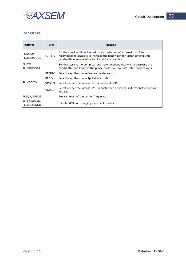
Registers
Register Bits Purpose
PLLLOOP
PLLLOOPBOOST FLT[1:0]
Synthesizer loop filter bandwidth and selection of external loop filter, recommended usage is to increase the bandwidth for faster settling time, bandwidth increases of factor 2 and 5 are possible.
PLLCPI
PLLCPIBOOST
Synthesizer charge pump current, recommended usage is to decrease the bandwidth (and improve the phase-noise) for low data-rate transmissions.
REFDIV Sets the synthesizer reference divider ratio.
RFDIV Sets the synthesizer output divider ratio.
VCOSEL Selects either the internal or the external VCO. PLLVCODIV
VCO2INT Selects either the internal VCO inductor or an external inductor between pins L1 and L2.
FREQA, FREQB Programming of the carrier frequency
PLLRANGINGA, PLLRANGINGB
Initiate VCO auto-ranging and check results
Version 1.10 Datasheet AX5043
Circuit Description 30
5.8. RF Input and Output Stage (ANTP/ANTN/ANTP1)
The AX5043 has two main antenna interface modes:
1. Both RX and TX use differential pins ANTP and ANTN. RX/TX switching is handled internally. This mode is recommended for highest output powers, highest sensitivities and for direct connection to dipole antennas. Also see Figure 13.
2. RX uses the differential antenna pins ANTP and ANTN. TX uses the single ended antenna pin ANTP1. RX/TX switching is handled externally. This can be done either with an external RX/TX switch or with a direct tie configuration. This mode is recommended for low output powers at high efficiency (Figure 16) and for usage with external power amplifiers (Figure 15).
Pin PWRAMP can be used to control an external RX/TX switch when operating the device together with an external PA (Figure 15). Pin ANTSEL can be used to control an external antenna switch when receiving with two antennas (Figure 17).
When antenna diversity is enabled, the radio controller will, when not in the middle of receiving a packet, periodically probe both antennas and select the antenna with the highest signal strength. The radio controller can be instructed to periodically write both RSSI values into the FIFO. Antenna diversity mode is fully automatic.
LNA
The LNA amplifies the differential RF signal from the antenna and buffers it to drive the I/Q mixer. An external matching network is used to adapt the antenna impedance to the IC impedance. A DC feed to GND must be provided at the antenna pins. For recommendations, see section 7: Application Information.
PA
In TX mode the PA drives the signal generated by the frequency generation subsystem out to either the differential antenna terminals or to the single ended antenna pin. The antenna terminals are chosen via the bits TXDIFF and TXSE in register MODECFGA.
The output power of the PA is programmed via the register TXPWRCOEFFB.
The PA can be digitally pre-distorted for high linearity.
The output amplitude can be shaped (raised cosine), this mode is selected with bit AMPLSHAPE in register MODECFGA. PA ramping is programmable in increments of the bit time and can be set to 1 – 8 bit times via bits SLOWRAMP in register MODECFGA.
Output power as well as harmonic content will depend on the external impedance seen by the PA, recommendations are given in the section 7: Application Information.
Version 1.10 Datasheet AX5043
Circuit Description 31
5.9. Digital IF Channel Filter and Demodulator
The digital IF channel filter and the demodulator extract the data bit-stream from the incoming IF signal. They must be programmed to match the modulation scheme as well as the data-rate. Inaccurate programming will lead to loss of sensitivity.
The channel filter offers bandwidths of 995 Hz up to 221 kHz.
The AXSEM RadioLab software calculates the necessary register settings for optimal performance and details can be found in the AX5043 Programming Manual. An overview of the registers involved is given in the following table as reference. The register setups typically must be done once at power-up of the device.
Registers
Register Remarks
DECIMATION This register programs the bandwidth of the digital channel filter.
RXDATARATE2… RXDATARATE0 These registers specify the receiver bit rate, relative to the channel filter bandwidth.
MAXDROFFSET2…MAXDROFFSET0 These registers specify the maximum possible data rate offset.
MAXRFOFFSET2…MAXRFOFFSET0 These registers specify the maximum possible RF frequency offset.
TIMEGAIN,DRGAIN
These registers specify the aggressiveness of the receiver bit timing recovery. More aggressive settings allow the receiver to synchronize with shorter preambles, at the expense of more timing jitter and thus a higher bit error rate at a given signal-to-noise ratio.
MODULATION This register selects the modulation to be used by the transmitter and the receiver, i.e. whether ASK, FSK should be used.
PHASEGAIN, FREQGAINA, FREQGAINB, FREQGAINC, FREQGAIND, AMPLGAIN
These registers control the bandwidth of the phase, frequency offset and amplitude tracking loops.
AGCGAIN This register controls the AGC (automatic gain control) loop slopes, and thus the speed of gain adjustments. The faster the bit-rate, the faster the AGC loop should be.
TXRATE These registers control the bit rate of the transmitter.
FSKDEV
These registers control the frequency deviation of the transmitter in FSK mode. The receiver does not explicitly need to know the frequency deviation, only the channel filter bandwidth has to be set wide enough for the complete modulation to pass.
Version 1.10 Datasheet AX5043
Circuit Description 32
5.10. Encoder
The encoder is located between the Framing Unit, the Demodulator and the Modulator. It can optionally transform the bit-stream in the following ways:
• It can invert the bit stream.
• It can perform differential encoding. This means that a zero is transmitted as no change in the level, and a one is transmitted as a change in the level.
• It can perform Manchester encoding. Manchester encoding ensures that the modulation has no DC content and enough transitions (changes from 0 to 1 and from 1 to 0) for the demodulator bit timing recovery to function correctly, but does so at a doubling of the data rate.
• It can perform spectral shaping (also know as whitening). Spectral shaping removes DC content of the bit stream, ensures transitions for the demodulator bit timing recovery, and makes sure that the transmitted spectrum does not have discrete lines even if the transmitted data is cyclic. It does so without adding additional bits, i.e. without changing the data rate. Spectral Shaping uses a self synchronizing feedback shift register.
The encoder is programmed using the register ENCODING, details and recommendations on usage are given in the AX5043 Programming Manual.
5.11. Framing and FIFO
Most radio systems today group data into packets. The Framing Unit is responsible for converting these packets into a bit-stream suitable for the modulator, and to extract packets from the continuous bit-stream arriving from the demodulator.
The Framing Unit supports two different modes:
• Packet modes
• Raw modes
The micro-controller communicates with the framing unit through a 256 byte FIFO. Data in the FIFO is organized in Chunks. The chunk header encodes the length and what data is contained in the payload. Chunks may contain packet data, but also RSSI, Frequency Offset, Timestamps, etc.
The AX5043 contains one FIFO. Its direction is switched depending on whether transmit or receive mode is selected.
The FIFO can be operated in polled or interrupt driven modes. In polled mode, the micro-controller must periodically read the FIFO status register or the FIFO count register to determine whether the FIFO needs servicing.
Version 1.10 Datasheet AX5043
Circuit Description 33
In interrupt mode EMPTY, NOT EMPTY, FULL, NOT FULL and programmable level interrupts are provided. The AX5043 signals interrupts by asserting (driving high) its IRQ line. The interrupt line is level triggered, active high. Interrupts are acknowledged by removing the cause for the interrupt, i.e. by emptying or filling the FIFO.
Basic FIFO status (EMPTY, FULL, Overrun, Underrun, FIFO fill level above threshold, FIFO free space above threshold) are also provided during each SPI access on MISO while the micro- controller shifts out the register address on MOSI. See the SPI interface section for details. This feature significantly reduces the number of SPI accesses necessary during transmit and receive.
Packet Modes
The AX5043 offers different packet modes. For arbitrary packet sizes HDLC is recommended since the flag and bit-stuffing mechanism. The AX5043 also offers packet modes with fixed packet length with a byte indicating the length of the packet.
In packet modes a CRC can be computed automatically.
HDLC1 Mode is the main framing mode of the AX5043. In this mode, the AX5043 performs automatic packet delimiting, and optional packet correctness check by inserting and checking a cyclic redundancy check (CRC) field.
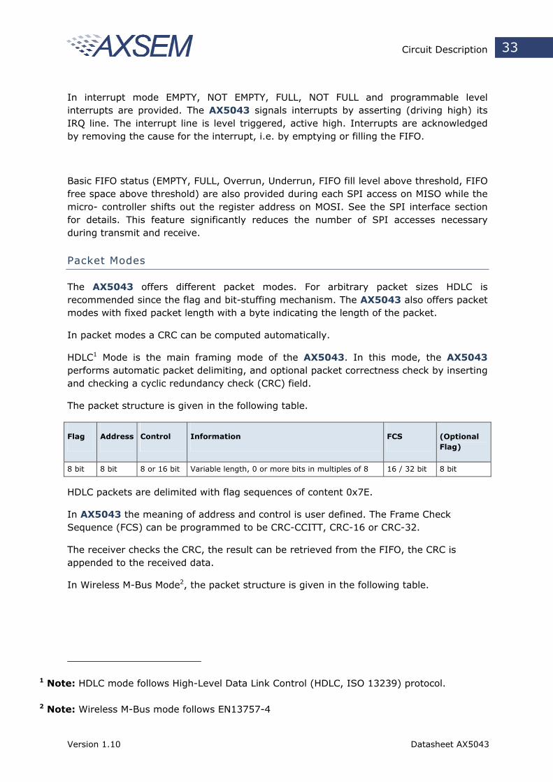
The packet structure is given in the following table.
Flag Address Control Information FCS (Optional Flag)
8 bit 8 bit 8 or 16 bit Variable length, 0 or more bits in multiples of 8 16 / 32 bit 8 bit
HDLC packets are delimited with flag sequences of content 0x7E.
In AX5043 the meaning of address and control is user defined. The Frame Check Sequence (FCS) can be programmed to be CRC-CCITT, CRC-16 or CRC-32.
The receiver checks the CRC, the result can be retrieved from the FIFO, the CRC is appended to the received data.
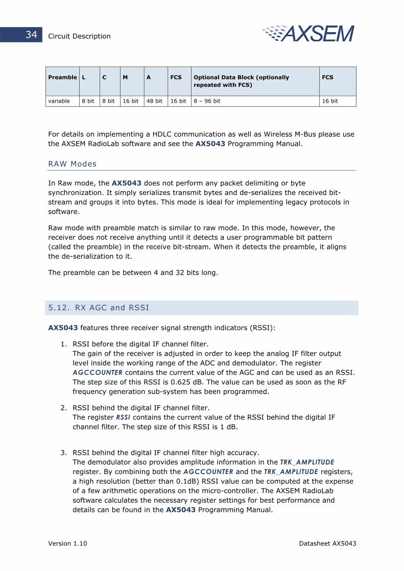
In Wireless M-Bus Mode2, the packet structure is given in the following table.
1 Note: HDLC mode follows High-Level Data Link Control (HDLC, ISO 13239) protocol.
2 Note: Wireless M-Bus mode follows EN13757-4
Version 1.10 Datasheet AX5043
Circuit Description 34
Preamble L C M A FCS Optional Data Block (optionally repeated with FCS)
FCS
variable 8 bit 8 bit 16 bit 48 bit 16 bit 8 – 96 bit 16 bit
For details on implementing a HDLC communication as well as Wireless M-Bus please use the AXSEM RadioLab software and see the AX5043 Programming Manual.
RAW Modes
In Raw mode, the AX5043 does not perform any packet delimiting or byte synchronization. It simply serializes transmit bytes and de-serializes the received bit-stream and groups it into bytes. This mode is ideal for implementing legacy protocols in software.
Raw mode with preamble match is similar to raw mode. In this mode, however, the receiver does not receive anything until it detects a user programmable bit pattern (called the preamble) in the receive bit-stream. When it detects the preamble, it aligns the de-serialization to it.
The preamble can be between 4 and 32 bits long.
5.12. RX AGC and RSSI
AX5043 features three receiver signal strength indicators (RSSI):
1. RSSI before the digital IF channel filter. The gain of the receiver is adjusted in order to keep the analog IF filter output level inside the working range of the ADC and demodulator. The register AGCCOUNTER contains the current value of the AGC and can be used as an RSSI. The step size of this RSSI is 0.625 dB. The value can be used as soon as the RF frequency generation sub-system has been programmed.
2. RSSI behind the digital IF channel filter. The register RSSI contains the current value of the RSSI behind the digital IF channel filter. The step size of this RSSI is 1 dB.
3. RSSI behind the digital IF channel filter high accuracy. The demodulator also provides amplitude information in the TRK_AMPLITUDE register. By combining both the AGCCOUNTER and the TRK_AMPLITUDE registers, a high resolution (better than 0.1dB) RSSI value can be computed at the expense of a few arithmetic operations on the micro-controller. The AXSEM RadioLab software calculates the necessary register settings for best performance and details can be found in the AX5043 Programming Manual.
Version 1.10 Datasheet AX5043
Circuit Description 35
5.13. Modulator
Depending on the transmitter settings the modulator generates various inputs for the PA:
Modulation Bit = 0 Bit = 1 Main Lobe Bandwidth
Max. Bitrate
ASK PA off PA on BW=BITRATE 115.2 kBit/s
FSK/MSK/GFSK/GMSK ∆f=-fdeviation ∆f=+fdeviation BW=(1+h) ⋅BITRATE 115.2 kBit/s
h = modulation index. It is the ratio of the deviation compared to the bit-rate; fdeviation = 0.5⋅h⋅BITRATE, AX5043 can demodulate signals with h < 32.
ASK = amplitude shift keying
FSK = frequency shift keying
MSK = minimum shift keying; MSK is a special case of FSK, where h = 0.5, and therefore fdeviation = 0.25⋅BITRATE; the advantage of MSK over FSK is that it can be demodulated more robustly.
All modulation schemes, except 4-FSK, are binary.
Amplitude can be shaped using a raised cosine waveform. Amplitude shaping will also be performed for constant amplitude modulation ((G)FSK, (G)MSK) for ramping up and down the PA. Amplitude shaping should always be enabled.
Frequency shaping can either be hard (FSK, MSK), or Gaussian (GMSK, GFSK), with selectable BT=0.3 or BT=0.5.
Modulation DiBit = 00 DiBit = 01 DiBit = 11 DiBit = 10 Main Lobe Bandwidth
Max. Bitrate
4-FSK ∆f=-3fdeviation ∆f=-fdeviation ∆f=+fdeviation ∆f=+3fdeviationBW=(1+3h) ⋅BITRATE
115.2 kBit/s
4-FSK Frequency shaping is always hard.
5.14. Automatic Frequency Control (AFC)
The AX5043 features an automatic frequency tracking loop which is capable of tracking the transmitter frequency within the RX filter band width. On top of that the AX5043 has a frequency tracking register TRKRFFREQ to synchronize the receiver frequency to a carrier signal. For AFC adjustment, the frequency offset can be computed with the following formula:
Version 1.10 Datasheet AX5043
Circuit Description 36
XTALfTRKRFFREQ
f242
=∆ .
The pull-in range of the AFC can be programmed with the MAXRFOFFSET Registers.
5.15. PWRMODE Register
The PWRMODE register controls, which parts of the chip are operating.
PWRMODE register
Name Description
0000 POWERDOWN
All digital and analog functions, except the register file, are disabled. The core supply voltages are switched off to conserve leakage power. Register contents are preserved and accessible registers via SPI, but at a slower speed.
Access to the FIFO is not possible and the contents are not preserved. POWERDOWN mode is only entered once the FIFO is empty.
0001 DEEPSLEEP
AX5043 is fully turned off. All digital and analog functions are disabled. All register contents are lost.
To leave DEEPSLEEP mode the pin SEL has to be pulled low. This will initiate startup and reset of the AX5043. Then the MISO line should be polled, as it will be held low during initialization and will rise to high at the end of the initialization, when the chip becomes ready for operation.
0101 STANDBY
The crystal oscillator and the reference are powered on; receiver and transmitter are off. Register contents are preserved and accessible registers via SPI. Access to the FIFO is not possible and the contents are not preserved. STANDBY is only entered once the FIFO is empty.
0110 FIFO The reference is powered on. Register contents are preserved and accessible registers via SPI. Access to the FIFO is possible and the contents are preserved.
1000 SYNTHRX The synthesizer is running on the receive frequency. Transmitter and receiver are still off. This mode is used to let the synthesizer settle on the correct frequency for receive.
1001 FULLRX Synthesizer and receiver are running.
1011 WOR Receiver wakeup-on-radio mode. The mode the same as POWERDOWN, but the 640 Hz internal low power oscillator is running.
1100 SYNTHTX The synthesizer is running on the transmit frequency. Transmitter and receiver are still off. This mode is used to let the synthesizer settle on the correct frequency for transmit.
1101 FULLTX Synthesizer and transmitter are running. Do not switch into this mode before the synthesizer has completely settled on the transmit frequency (in SYNTHTX mode), otherwise spurious spectral transmissions will occur.
For the corresponding currents see table in section 4.2.
Version 1.10 Datasheet AX5043
Circuit Description 37
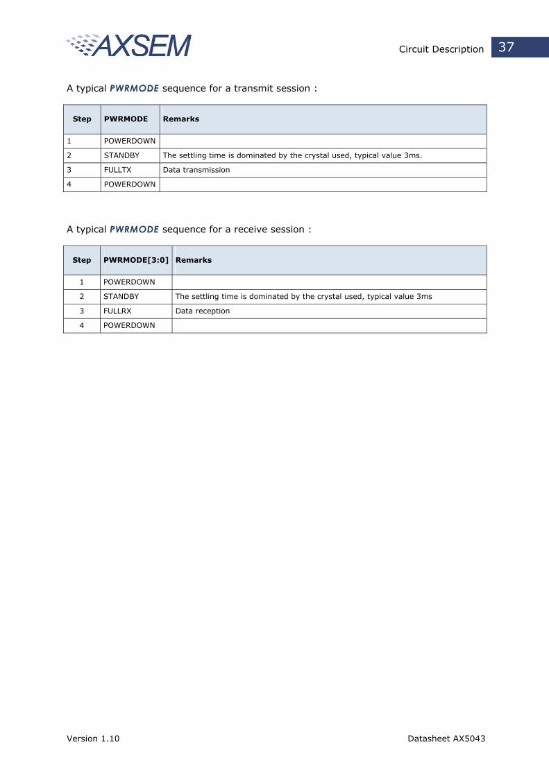
A typical PWRMODE sequence for a transmit session :
Step PWRMODE Remarks
1 POWERDOWN
2 STANDBY The settling time is dominated by the crystal used, typical value 3ms.
3 FULLTX Data transmission
4 POWERDOWN
A typical PWRMODE sequence for a receive session :
Step PWRMODE[3:0] Remarks
1 POWERDOWN
2 STANDBY The settling time is dominated by the crystal used, typical value 3ms
3 FULLRX Data reception
4 POWERDOWN
Version 1.10 Datasheet AX5043
Circuit Description 38
5.16. Serial Peripheral Interface (SPI)
The AX5043 can be programmed via a four wire serial interface according SPI using the pins CLK, MOSI, MISO and SEL. Registers for setting up the AX5043 are programmed via the serial peripheral interface in all device modes.
When the interface signal SEL is pulled low, a configuration data stream is expected on the input signal pin MOSI, which is interpreted as D0...Dx, A0...Ax, R_N/W. Data read from the interface appears on MISO.
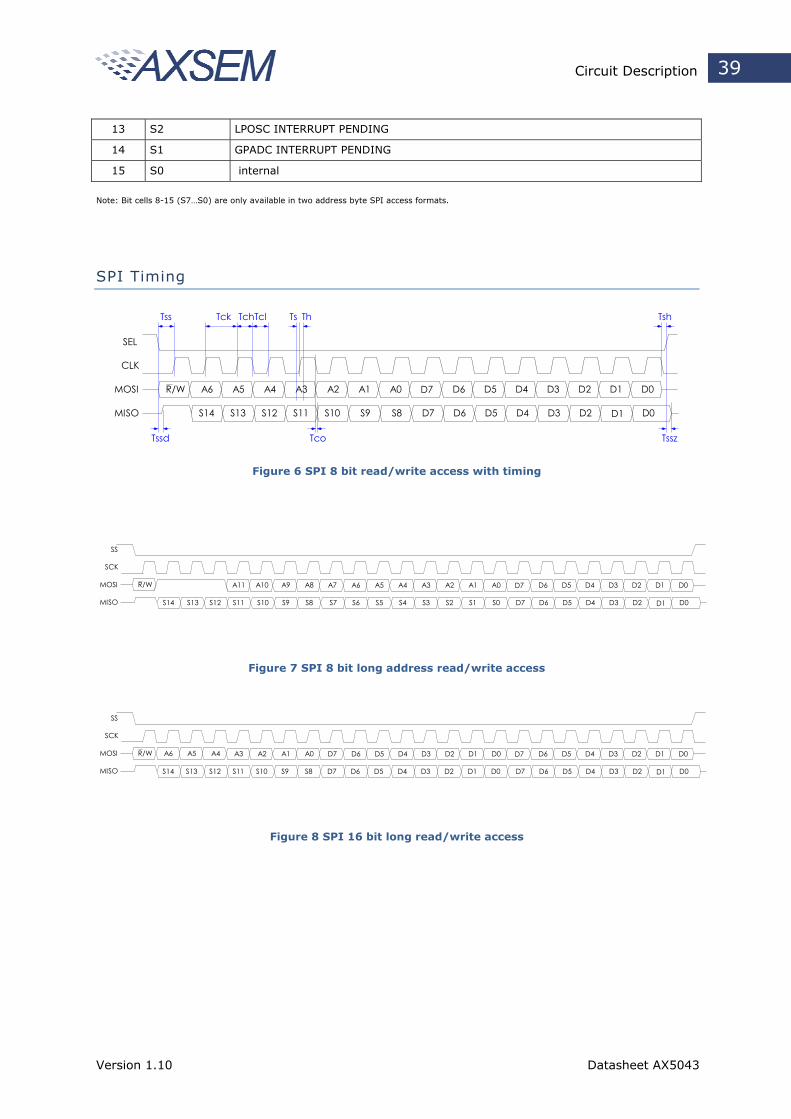
Figure 6 shows a write/read access to the interface. The data stream is built of an address byte including read/write information and a data byte. Depending on the R_N/W bit and address bits A[6..0], data D[7..0] can be written via MOSI or read at the pin MISO. R_N/W = 0 means read mode, R_N/W = 1 means write mode.
Most registers are 8 bits wide and accessed using the waveforms as detailed in Figure 7. The most important registers are at the beginning of the address space, i.e. at addresses less than 0x70. These registers can be accessed more efficiently using the short address form, which is detailed in Figure 6.
Some registers are longer than 8 bits. These registers can be accessed more quickly than by reading and writing individual 8 bit parts. This is illustrated in Figure 8. Accesses are not limited by 16 bits either, reading and writing data bytes can be continued as long as desired. After each byte, the address counter is incremented by one. Also, this access form works with long addresses.
During the address phase of the access, the AX5043 outputs the most important status bits. This feature is designed to speed up the software decision on what to do in an interrupt handler.
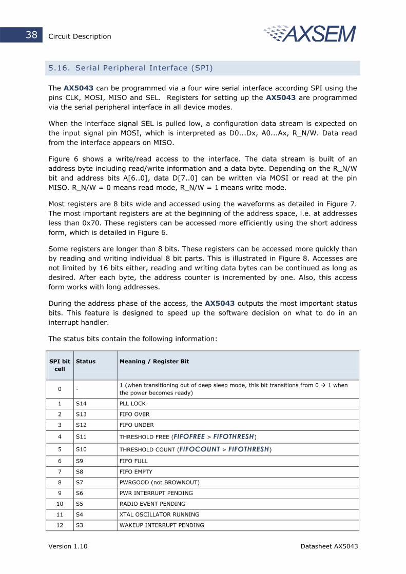
The status bits contain the following information:
SPI bit cell
Status Meaning / Register Bit
0 - 1 (when transitioning out of deep sleep mode, this bit transitions from 0 1 when the power becomes ready)
1 S14 PLL LOCK
2 S13 FIFO OVER
3 S12 FIFO UNDER
4 S11 THRESHOLD FREE (FIFOFREE > FIFOTHRESH)
5 S10 THRESHOLD COUNT (FIFOCOUNT > FIFOTHRESH)
6 S9 FIFO FULL
7 S8 FIFO EMPTY
8 S7 PWRGOOD (not BROWNOUT)
9 S6 PWR INTERRUPT PENDING
10 S5 RADIO EVENT PENDING
11 S4 XTAL OSCILLATOR RUNNING
12 S3 WAKEUP INTERRUPT PENDING
Version 1.10 Datasheet AX5043
Circuit Description 39
13 S2 LPOSC INTERRUPT PENDING
14 S1 GPADC INTERRUPT PENDING
15 S0 internal
Note: Bit cells 8-15 (S7…S0) are only available in two address byte SPI access formats.
SPI Timing
Tsh
R/W
SEL
CLK
MOSI
MISO
A6 A5 A4 A3 A2 A1 D7A0 D6 D5 D4 D0D1D2D3
D7 D6 D5 D4 D3 D2 D1 D0S14 S13 S12 S11 S10 S9 S8
Tssd Tco
Tss Tck TchTcl ThTs
Tssz
Figure 6 SPI 8 bit read/write access with timing
R/W
SS
SCK
MOSI
MISO
A6 A5 A4 A3 A2 A1 D7A0 D6 D5 D4 D0D1D2D3
D7 D6 D5 D4 D3 D2 D1 D0S6 S5 S4 S3 S2 S1 S0
A11 A10 A9 A7A8
S7S14 S13 S12 S11 S10 S9 S8
Figure 7 SPI 8 bit long address read/write access
R/W
SS
SCK
MOSI
MISO
D6 D5 D4 D3 D2 D1 D7D0 D6 D5 D4 D0D1D2D3
D7 D6 D5 D4 D3 D2 D1 D0D6 D5 D4 D3 D2 D1 D0
A3 A2 A1 D7A0
D7S14 S13 S12 S11 S10 S9 S8
A6 A5 A4
Figure 8 SPI 16 bit long read/write access
Version 1.10 Datasheet AX5043
Circuit Description 40
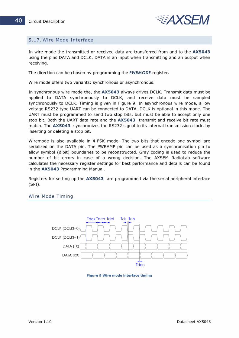
5.17. Wire Mode Interface
In wire mode the transmitted or received data are transferred from and to the AX5043 using the pins DATA and DCLK. DATA is an input when transmitting and an output when receiving.
The direction can be chosen by programming the PWRMODE register.
Wire mode offers two variants: synchronous or asynchronous.
In synchronous wire mode the, the AX5043 always drives DCLK. Transmit data must be applied to DATA synchronously to DCLK, and receive data must be sampled synchronously to DCLK. Timing is given in Figure 9. In asynchronous wire mode, a low voltage RS232 type UART can be connected to DATA. DCLK is optional in this mode. The UART must be programmed to send two stop bits, but must be able to accept only one stop bit. Both the UART data rate and the AX5043 transmit and receive bit rate must match. The AX5043 synchronizes the RS232 signal to its internal transmission clock, by inserting or deleting a stop bit.
Wiremode is also available in 4-FSK mode. The two bits that encode one symbol are serialized on the DATA pin. The PWRAMP pin can be used as a synchronisation pin to allow symbol (dibit) boundaries to be reconstructed. Gray coding is used to reduce the number of bit errors in case of a wrong decision. The AXSEM RadioLab software calculates the necessary register settings for best performance and details can be found in the AX5043 Programming Manual.
Registers for setting up the AX5043 are programmed via the serial peripheral interface (SPI).
Wire Mode Timing
Tdh
DCLK (DCLKI=0)
DATA (RX)
DCLK (DCLKI=1)
Tdco
DATA (TX)
Tdch TdclTdck Tds
Figure 9 Wire mode interface timing
Version 1.10 Datasheet AX5043
Circuit Description 41
5.18. General Purpose ADC (GPADC)
The AX5043 features a general purpose ADC. The ADC input pins are GPADC1 and GPADC2. The ADC converts the voltage difference applied between pins GPADC1 and GPADC2. If pin GPADC2 is left open, the ADC converts the difference between an internally generated value of 800 mV and the voltage applied at pin GPADC1.
The GPADC can only be used if the receiver is disabled. To enable the GPADC write 1 to the GPADC13 bit in the GPADCCTRL register. To start a single conversion, write 1 to the BUSY bit in the GPADCCTRL register. Then wait for the BUSY bit to clear, or the GPADC Interrupt to be asserted. The GPADC Interrupt is cleared by reading the result register GPADC13VALUE.
If continuous sampling is desired, set the CONT bit in register GPADCCTRL. The desired sampling rate can be specified in the GPADCPERIOD register.
5.19. Σ∆ DAC
One digital Pin (ANTSEL or PWRAMP) may be used as a Σ∆ Digital-to-Analog Converter. A simple RC lowpass filter is needed to smooth the output. The DAC may be used to output RSSI, many demodulator variables, or a constant value under software control.
Version 1.10 Datasheet AX5043
Register Bank Description 42
6. Register Bank Description
This section describes the bits of the register bank as reference. The registers are grouped by functional block to facilitate programming. The AXSEM RadioLab software calculates the necessary register settings for best performance and details can be found in the AX5043 Programming Manual.
An R in the retention column means that this register’s contents are not lost during power-down mode.
No checks are made whether the programmed combination of bits makes sense! Bit 0 is always the LSB.
Note Whole registers or register bits marked as reserved should be kept at their default values.
Note All addresses not documented here must not be accessed, neither in reading nor in writing.
Note The retention column indicates if the register contents are preserved in power-down mode.
Version 1.10 Datasheet AX5043
Register Bank Description 43
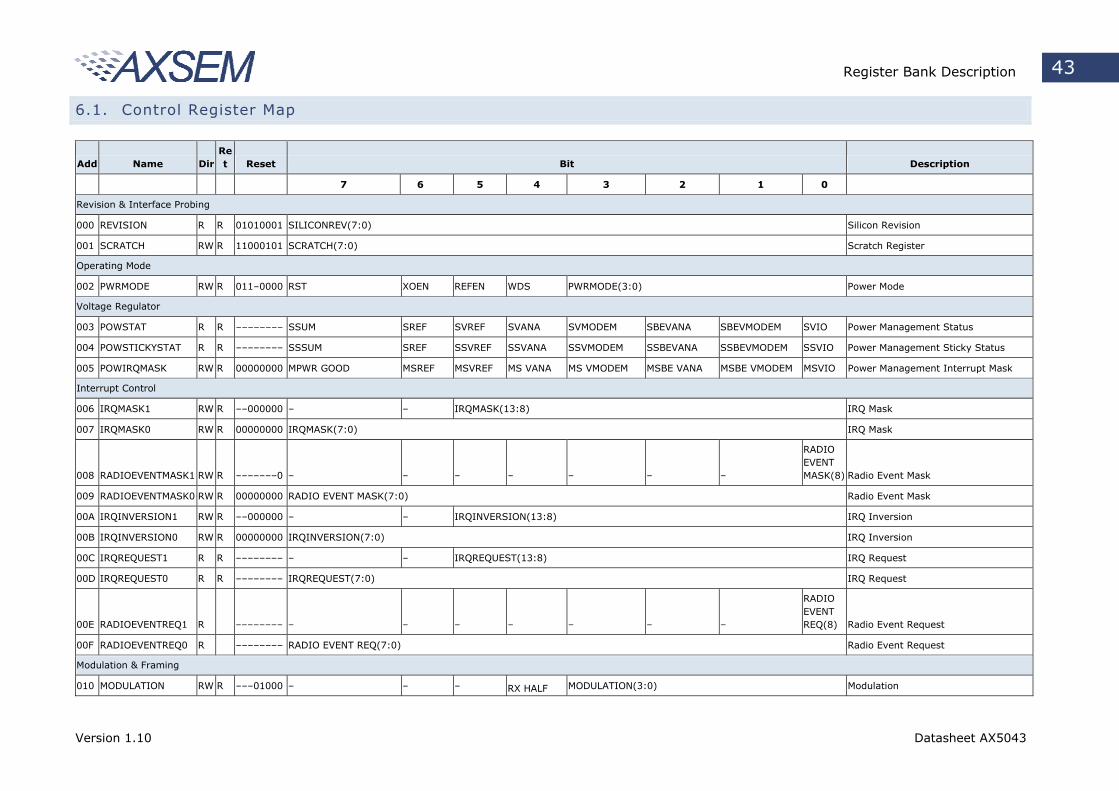
6.1. Control Register Map
Add Name Dir Ret Reset Bit Description
7 6 5 4 3 2 1 0
Revision & Interface Probing
000 REVISION R R 01010001 SILICONREV(7:0) Silicon Revision
001 SCRATCH RW R 11000101 SCRATCH(7:0) Scratch Register
Operating Mode
002 PWRMODE RW R 011–0000 RST XOEN REFEN WDS PWRMODE(3:0) Power Mode
Voltage Regulator
003 POWSTAT R R –––––––– SSUM SREF SVREF SVANA SVMODEM SBEVANA SBEVMODEM SVIO Power Management Status
004 POWSTICKYSTAT R R –––––––– SSSUM SREF SSVREF SSVANA SSVMODEM SSBEVANA SSBEVMODEM SSVIO Power Management Sticky Status
005 POWIRQMASK RW R 00000000 MPWR GOOD MSREF MSVREF MS VANA MS VMODEM MSBE VANA MSBE VMODEM MSVIO Power Management Interrupt Mask
Interrupt Control
006 IRQMASK1 RW R ––000000 – – IRQMASK(13:8) IRQ Mask
007 IRQMASK0 RW R 00000000 IRQMASK(7:0) IRQ Mask
008 RADIOEVENTMASK1 RW R –––––––0 – – – – – – –
RADIO EVENT MASK(8) Radio Event Mask
009 RADIOEVENTMASK0 RW R 00000000 RADIO EVENT MASK(7:0) Radio Event Mask
00A IRQINVERSION1 RW R ––000000 – – IRQINVERSION(13:8) IRQ Inversion
00B IRQINVERSION0 RW R 00000000 IRQINVERSION(7:0) IRQ Inversion
00C IRQREQUEST1 R R –––––––– – – IRQREQUEST(13:8) IRQ Request
00D IRQREQUEST0 R R –––––––– IRQREQUEST(7:0) IRQ Request
00E RADIOEVENTREQ1 R –––––––– – – – – – – –
RADIO EVENT REQ(8) Radio Event Request
00F RADIOEVENTREQ0 R –––––––– RADIO EVENT REQ(7:0) Radio Event Request
Modulation & Framing
010 MODULATION RW R –––01000 – – – RX HALF MODULATION(3:0) Modulation
Version 1.10 Datasheet AX5043
Register Bank Description 44
SPEED
011 ENCODING RW R –––00010 – – – ENC NOSYNC ENC MANCH ENC SCRAM ENC DIFF ENC INV Encoder/Decoder Settings
012 FRAMING RW R –0000000 FRMRX CRCMODE(2:0) FRMMODE(2:0) FABORT Framing settings
014 CRCINIT3 RW R 11111111 CRCINIT(31:24) CRC Initialisation Data
015 CRCINIT2 RW R 11111111 CRCINIT(23:16) CRC Initialisation Data
016 CRCINIT1 RW R 11111111 CRCINIT(15:8) CRC Initialisation Data
017 CRCINIT0 RW R 11111111 CRCINIT(7:0) CRC Initialisation Data
Forward Error Correction
018 FEC RW R 00000000 SHORT MEM RSTVI TERBI FEC NEG FEC POS FECINPSHIFT(2:0) FEC ENA FEC (Viterbi) Configuration
019 FECSYNC RW R 01100010 FECSYNC(7:0) Interleaver Synchronisation Threshold
01A FECSTATUS R R –––––––– FEC INV MAXMETRIC(6:0) FEC Status
Status
01C RADIOSTATE R – ––––0000 – – – – RADIOSTATE(3:0) Radio Controller State
01D XTALSTATUS R R –––––––– – – – – – – – XTAL RUN Crystal Oscillator Status
Pin Configuration
020 PINSTATE R R –––––––– – – PS PWR AMP PS ANT SEL PS IRQ PS DATA PS DCLK
PS SYS CLK Pinstate
021 PINFUNCSYSCLK RW R 0––01000 PU SYSCLK – – PFSYSCLK(4:0) SYSCLK Pin Function
022 PINFUNCDCLK RW R 00–––100 PU DCLK PI DCLK – – – PFDCLK(2:0) DCLK Pin Function
023 PINFUNCDATA RW R 10–––111 PU DATA PI DATA – – – PFDATA(2:0) DATA Pin Function
024 PINFUNCIRQ RW R 00–––011 PU IRQ PI IRQ – – – PFIRQ(2:0) IRQ Pin Function
025 PINFUNCANTSEL RW R 00–––110 PU ANTSEL PI ANTSEL – – – PFANTSEL(2:0) ANTSEL Pin Function
026 PINFUNCPWRAMP RW R 00––0110 PU PWRAMP PI PWRAMP – – PFPWRAMP(3:0) PWRAMP Pin Function
027 PWRAMP RW R –––––––0 – – – – – – – PWRAMP PWRAMP Control
FIFO
028 FIFOSTAT R R 0––––––– FIFO AUTO COMMIT – FIFO FREE THR
FIFO CNT THR FIFO OVER FIFO UNDER FIFO FULL
FIFO EMPTY FIFO Control
Version 1.10 Datasheet AX5043
Register Bank Description 45
W R FIFOCMD(5:0)
029 FIFODATA RW –––––––– FIFODATA(7:0) FIFO Data
02A FIFOCOUNT1 R R –––––––0 – – – – – – –
FIFO COUNT(8) Number of Words currently in FIFO
02B FIFOCOUNT0 R R 00000000 FIFOCOUNT(7:0) Number of Words currently in FIFO
02C FIFOFREE1 R R –––––––1 – – – – – – – FIFO FREE(8)
Number of Words that can be written to FIFO
02D FIFOFREE0 R R 00000000 FIFOFREE(7:0) Number of Words that can be written to FIFO
02E FIFOTHRESH1 RW R –––––––0 – – – – – – –
FIFO THRESH(8) FIFO Threshold
02F FIFOTHRESH0 RW R 00000000 FIFOTHRESH(7:0) FIFO Threshold
Synthesizer
030 PLLLOOP RW R 0–––1001 FREQB – – – DIRECT FILT EN FLT(1:0) PLL Loop Filter Settings
031 PLLCPI RW R 00001000 PLLCPI PLL Charge Pump Current (Boosted)
032 PLLVCODIV RW R –000–000 – VCOI MAN VCO2INT VCOSEL – RFDIV REFDIV(1:0) PLL Divider Settings
033 PLLRANGINGA RW R 00001000 STICKY LOCK PLL LOCK RNGERR RNG START VCORA(3:0) PLL Autoranging
034 FREQA3 RW R 00111001 FREQA(31:24) Synthesizer Frequency
035 FREQA2 RW R 00110100 FREQA(23:16) Synthesizer Frequency
036 FREQA1 RW R 11001100 FREQA(15:8) Synthesizer Frequency
037 FREQA0 RW R 11001101 FREQA(7:0) Synthesizer Frequency
038 PLLLOOPBOOST RW R 0–––1011 FREQB – – – DIRECT FILT EN FLT(1:0) PLL Loop Filter Settings (Boosted)
039 PLLCPIBOOST RW R 11001000 PLLCPI PLL Charge Pump Current
03B PLLRANGINGB RW R 00001000 STICKY LOCK PLL LOCK RNGERR RNG START VCORB(3:0) PLL Autoranging
03C FREQB3 RW R 00111001 FREQB(31:24) Synthesizer Frequency
03D FREQB2 RW R 00110100 FREQB(23:16) Synthesizer Frequency
03E FREQB1 RW R 11001100 FREQB(15:8) Synthesizer Frequency
03F FREQB0 RW R 11001101 FREQB(7:0) Synthesizer Frequency
Signal Strength
Version 1.10 Datasheet AX5043
Register Bank Description 46
040 RSSI R R –––––––– RSSI(7:0) Received Signal Strength Indicator
041 BGNDRSSI RW R 00000000 BGNDRSSI(7:0) Background RSSI
042 DIVERSITY RW R ––––––00 – – – – – – ANT SEL DIV ENA Antenna Diversity Configuration
043 AGCCOUNTER RW R –––––––– AGCCOUNTER(7:0) AGC Current Value
Receiver Tracking
045 TRKDATARATE2 R R –––––––– TRKDATARATE(23:16) Datarate Tracking
046 TRKDATARATE1 R R –––––––– TRKDATARATE(15:8) Datarate Tracking
047 TRKDATARATE0 R R –––––––– TRKDATARATE(7:0) Datarate Tracking
048 TRKAMPL1 R R –––––––– TRKAMPL(15:8) Amplitude Tracking
049 TRKAMPL0 R R –––––––– TRKAMPL(7:0) Amplitude Tracking
04A TRKPHASE1 R R –––––––– – – – – TRKPHASE(11:8) Phase Tracking
04B TRKPHASE0 R R –––––––– TRKPHASE(7:0) Phase Tracking
04D TRKRFFREQ2 RW R –––––––– – – – – TRRFKFREQ(19:16) RF Frequency Tracking
04E TRKRFFREQ1 RW R –––––––– TRRFKFREQ(15:8) RF Frequency Tracking
04F TRKRFFREQ0 RW R –––––––– TRRFKFREQ(7:0) RF Frequency Tracking
050 TRKFREQ1 RW R –––––––– TRKFREQ(15:8) Frequency Tracking
051 TRKFREQ0 RW R –––––––– TRKFREQ(7:0) Frequency Tracking
052 TRKFSKDEMOD1 R R –––––––– – – TRKFSKDEMOD(13:8) FSK Demodulator Tracking
053 TRKFSKDEMOD0 R R –––––––– TRKFSKDEMOD(7:0) FSK Demodulator Tracking
054 TRKAFSKDEMOD1 R R –––––––– TRKAFSKDEMOD(15:8) AFSK Demodulator Tracking
055 TRKAFSKDEMOD0 R R –––––––– TRKAFSKDEMOD(7:0) AFSK Demodulator Tracking
Timer
059 TIMER2 R – –––––––– TIMER(23:16) 1MHz Timer
05A TIMER1 R – –––––––– TIMER(15:8) 1MHz Timer
05B TIMER0 R – –––––––– TIMER(7:0) 1MHz Timer
Wakeup Timer
068 WAKEUPTIMER1 R R –––––––– WAKEUPTIMER(15:8) Wakeup Timer
069 WAKEUPTIMER0 R R –––––––– WAKEUPTIMER(7:0) Wakeup Timer
06A WAKEUP1 RW R 00000000 WAKEUP(15:8) Wakeup Time
Version 1.10 Datasheet AX5043
Register Bank Description 47
06B WAKEUP0 RW R 00000000 WAKEUP(7:0) Wakeup Time
06C WAKEUPFREQ1 RW R 00000000 WAKEUPFREQ(15:8) Wakeup Frequency
06D WAKEUPFREQ0 RW R 00000000 WAKEUPFREQ(7:0) Wakeup Frequency
06E WAKEUPXOEARLY RW R 00000000 WAKEUPXOEARLY Wakeup Crystal Oscillator Early
Physical Layer Parameters
Receiver Parameters
100 IFFREQ1 RW R 00010001 IFFREQ(15:8) 2nd LO / IF Frequency
101 IFFREQ0 RW R 00100111 IFFREQ(7:0) 2nd LO / IF Frequency
102 DECIMATION RW R –0001101 – DECIMATION(6:0) Decimation Factor
103 RXDATARATE2 RW R 00000000 RXDATARATE(23:16) Receiver Datarate
104 RXDATARATE1 RW R 00111101 RXDATARATE(15:8) Receiver Datarate
105 RXDATARATE0 RW R 10001010 RXDATARATE(7:0) Receiver Datarate
106 MAXDROFFSET2 RW R 00000000 MAXDROFFSET(23:16) Maximum Receiver Datarate Offset
107 MAXDROFFSET1 RW R 00000000 MAXDROFFSET(15:8) Maximum Receiver Datarate Offset
108 MAXDROFFSET0 RW R 10011110 MAXDROFFSET(7:0) Maximum Receiver Datarate Offset
109 MAXRFOFFSET2 RW R 0–––0000 FREQ OFFS CORR – – – MAXRFOFFSET(19:16) Maximum Receiver RF Offset
10A MAXRFOFFSET1 RW R 00010110 MAXRFOFFSET(15:8) Maximum Receiver RF Offset
10B MAXRFOFFSET0 RW R 10000111 MAXRFOFFSET(7:0) Maximum Receiver RF Offset
10C FSKDMAX1 RW R 00000000 FSKDEVMAX(15:8) Four FSK Rx Deviation
10D FSKDMAX0 RW R 10000000 FSKDEVMAX(7:0) Four FSK Rx Deviation
10E FSKDMIN1 RW R 11111111 FSKDEVMIN(15:8) Four FSK Rx Deviation
10F FSKDMIN0 RW R 10000000 FSKDEVMIN(7:0) Four FSK Rx Deviation
110 AFSKSPACE1 RW R ––––0000 – – – – AFSKSPACE(11:8) AFSK Space (0) Frequency
111 AFSKSPACE0 RW R 01000000 AFSKSPACE(7:0) AFSK Space (0) Frequency
112 AFSKMARK1 RW R ––––0000 – – – – AFSKMARK(11:8) AFSK Mark (1) Frequency
113 AFSKMARK0 RW R 01110101 AFSKMARK(7:0) AFSK Mark (1) Frequency
114 AFSKCTRL RW R –––00100 – – – AFSKSHIFT0(4:0) AFSK Control
115 AMPLFILTER RW R ––––0000 – – – – AMPLFILTER(3:0) Amplitude Filter
116 FREQUENCYLEAK RW R ––––0000 – – – – FREQUENCYLEAK[3:0] Baseband Frequency Recovery Loop
Version 1.10 Datasheet AX5043
Register Bank Description 48
Leakiness
117 RXPARAMSETS RW R 00000000 RXPS3(1:0) RXPS2(1:0) RXPS1(1:0) RXPS0(1:0) Receiver Parameter Set Indirection
118 RXPARAMCURSET R R –––––––– – – – RXSI(2) RXSN(1:0) RXSI(1:0) Receiver Parameter Current Set
Receiver Parameter Set 0
120 AGCGAIN0 RW R 10110100 AGCDECAY0(3:0) AGCATTACK0(3:0) AGC Speed
121 AGCTARGET0 RW R 01110110 AGCTARGET0(7:0) AGC Target
122 AGCAHYST0 RW R –––––000 - AGCAHYST0(2:0) AGC Digital Threshold Range
123 AGCMINMAX0 RW R –000–000 - AGCMAXDA0(2:0) - AGCMINDA0(2:0) AGC Digital Min/Max Set Points
124 TIMEGAIN0 RW R 11111000 TIMEGAIN0M TIMEGAIN0E Timing Gain
125 DRGAIN0 RW R 11110010 DRGAIN0M DRGAIN0E Data Rate Gain
126 PHASEGAIN0 RW R 11––0011 FILTERIDX0(1:0) – – PHASEGAIN0(3:0) Filter Index, Phase Gain
127 FREQGAINA0 RW R 00001111 FREQ LIM0 FREQ MODULO0
FREQ HALFMOD0
FREQ AMPL GATE0 FREQGAINA0(3:0) Frequency Gain A
128 FREQGAINB0 RW R 00–11111 FREQ FREEZE0 FREQ AVG0 – FREQGAINB0(4:0) Frequency Gain B
129 FREQGAINC0 RW R –––01010 – – – FREQGAINC0(4:0) Frequency Gain C
12A FREQGAIND0 RW R 0––01010 RFFREQ FREEZE0 – – FREQGAIND0(4:0) Frequency Gain D
12B AMPLGAIN0 RW R 01––0110 AMPL AVG AMPL AGC – – AMPLGAIN0(3:0) Amplitude Gain
12C FREQDEV10 RW R ––––0000 – – – – FREQDEV0(11:8) Receiver Frequency Deviation
12D FREQDEV00 RW R 00100000 FREQDEV0(7:0) Receiver Frequency Deviation
12E FOURFSK0 RW R –––10110 – – – DEV UPDATE0 DEVDECAY0(3:0) Four FSK Control
12F BBOFFSRES0 RW R 10001000 RESINTB0(3:0) RESINTA0(3:0) Baseband Offset Compensation Resistors
Receiver Parameter Set 1
130 AGCGAIN1 RW R 10110100 AGCDECAY1(3:0) AGCATTACK1(3:0) AGC Speed
131 AGCTARGET1 RW R 01110110 AGCTARGET1(7:0) AGC Target
132 AGCAHYST1 RW R –––––000 - AGCAHYST1(2:0) AGC Digital Threshold Range
133 AGCMINMAX1 RW R –000–000 - AGCMAXDA1(2:0) - AGCMINDA1(2:0) AGC Digital Min/Max Set Points
134 TIMEGAIN1 RW R 11110110 TIMEGAIN1M TIMEGAIN1E Timing Gain
Version 1.10 Datasheet AX5043
Register Bank Description 49
135 DRGAIN1 RW R 11110001 DRGAIN1M DRGAIN1E Data Rate Gain
136 PHASEGAIN1 RW R 11––0011 FILTERIDX1(1:0) – – PHASEGAIN1(3:0) Filter Index, Phase Gain
137 FREQGAINA1 RW R 00001111 FREQ LIM1 FREQ MODULO1
FREQ HALFMOD1
FREQ AMPL GATE1 FREQGAINA1(3:0) Frequency Gain A
138 FREQGAINB1 RW R 00–11111 FREQ FREEZE1 FREQ AVG1 – FREQGAINB1(4:0) Frequency Gain B
139 FREQGAINC1 RW R –––01011 – – – FREQGAINC1(4:0) Frequency Gain C
13A FREQGAIND1 RW R 0––01011 RFFREQ FREEZE1 – – FREQGAIND1(4:0) Frequency Gain D
13B AMPLGAIN1 RW R 01––0110 AMPL AVG1 AMPL1 AGC1 – – AMPLGAIN1(3:0) Amplitude Gain
13C FREQDEV11 RW R ––––0000 – – – – FREQDEV1(11:8) Receiver Frequency Deviation
13D FREQDEV01 RW R 00100000 FREQDEV1(7:0) Receiver Frequency Deviation
13E FOURFSK1 RW R –––11000 – – – DEV UPDATE1 DEVDECAY1(3:0) Four FSK Control
13F BBOFFSRES1 RW R 10001000 RESINTB1(3:0) RESINTA1(3:0) Baseband Offset Compensation Resistors
Receiver Parameter Set 2
140 AGCGAIN2 RW R 11111111 AGCDECAY2(3:0) AGCATTACK2(3:0) AGC Speed
141 AGCTARGET2 RW R 01110110 AGCTARGET2(7:0) AGC Target
142 AGCAHYST2 RW R –––––000 - AGCAHYST2(2:0) AGC Digital Threshold Range
143 AGCMINMAX2 RW R –000–000 - AGCMAXDA2(2:0) - AGCMINDA2(2:0) AGC Digital Min/Max Set Points
144 TIMEGAIN2 RW R 11110101 TIMEGAIN2M TIMEGAIN2E Timing Gain
145 DRGAIN2 RW R 11110000 DRGAIN2M DRGAIN2E Data Rate Gain
146 PHASEGAIN2 RW R 11––0011 FILTERIDX2(1:0) – – PHASEGAIN2(3:0) Filter Index, Phase Gain
147 FREQGAINA2 RW R 00001111 FREQ LIM2 FREQ MODULO2
FREQ HALFMOD2
FREQ AMPL GATE2 FREQGAINA2(3:0) Frequency Gain A
148 FREQGAINB2 RW R 00–11111 FREQ FREEZE2 FREQ AVG2 – FREQGAINB2(4:0) Frequency Gain B
149 FREQGAINC2 RW R –––01101 – – – FREQGAINC2(4:0) Frequency Gain C
14A FREQGAIND2 RW R 0––01101 RFFREQ FREEZE2 – – FREQGAIND2(4:0) Frequency Gain D
Version 1.10 Datasheet AX5043
Register Bank Description 50
14B AMPLGAIN2 RW R 01––0110 AMPL AVG2 AMPL AGC2 – – AMPLGAIN2(3:0) Amplitude Gain
14C FREQDEV12 RW R ––––0000 – – – – FREQDEV2(11:8) Receiver Frequency Deviation
14D FREQDEV02 RW R 00100000 FREQDEV2(7:0) Receiver Frequency Deviation
14E FOURFSK2 RW R –––11010 – – – DEV UPDATE2 DEVDECAY2(3:0) Four FSK Control
14F BBOFFSRES2 RW R 10001000 RESINTB2(3:0) RESINTA2(3:0) Baseband Offset Compensation Resistors
Receiver Parameter Set 3
150 AGCGAIN3 RW R 11111111 AGCDECAY3(3:0) AGCATTACK3(3:0) AGC Speed
151 AGCTARGET3 RW R 01110110 AGCTARGET3(7:0) AGC Target
152 AGCAHYST3 RW R –––––000 - AGCAHYST3(2:0) AGC Digital Threshold Range
153 AGCMINMAX3 RW R –000–000 - AGCMAXDA3(2:0) - AGCMINDA3(2:0) AGC Digital Min/Max Set Points
154 TIMEGAIN3 RW R 11110101 TIMEGAIN3M TIMEGAIN3E Timing Gain
155 DRGAIN3 RW R 11110000 DRGAIN3M DRGAIN3E Data Rate Gain
156 PHASEGAIN3 RW R 11––0011 FILTERIDX3(1:0) – – PHASEGAIN3(3:0) Filter Index, Phase Gain
157 FREQGAINA3 RW R 00001111 FREQ LIM3 FREQ MODULO3
FREQ HALFMOD3
FREQ AMPL GATE3 FREQGAINA3(3:0) Frequency Gain A
158 FREQGAINB3 RW R 00–11111 FREQ FREEZE3 FREQ AVG3 – FREQGAINB3(4:0) Frequency Gain B
159 FREQGAINC3 RW R –––01101 – – – FREQGAINC3(4:0) Frequency Gain C
15A FREQGAIND3 RW R 0––01101 RFFREQ FREEZE3 – – FREQGAIND3(4:0) Frequency Gain D
15B AMPLGAIN3 RW R 01––0110 AMPL AVG3 AMPL AGC3 – – AMPLGAIN3(3:0) Amplitude Gain
15C FREQDEV13 RW R ––––0000 – – – – FREQDEV3(11:8) Receiver Frequency Deviation
15D FREQDEV03 RW R 00100000 FREQDEV3(7:0) Receiver Frequency Deviation
15E FOURFSK3 RW R –––11010 – – – DEV UPDATE3 DEVDECAY3(3:0) Four FSK Control
15F BBOFFSRES3 RW R 10001000 RESINTB3(3:0) RESINTA3(3:0) Baseband Offset Compensation Resistors
Transmitter Parameters
Version 1.10 Datasheet AX5043
Register Bank Description 51
160 MODCFGF RW R ––––––00 – – – – – – FREQ SHAPE Modulator Configuration F
161 FSKDEV2 RW R 00000000 FSKDEV(23:16) FSK Frequency Deviation
162 FSKDEV1 RW R 00001010 FSKDEV(15:8) FSK Frequency Deviation
163 FSKDEV0 RW R 00111101 FSKDEV(7:0) FSK Frequency Deviation
164 MODCFGA RW R 0000–101 BROWN GATE PTTLCK GATE SLOW RAMP – AMPL SHAPE TX SE TX DIFF Modulator Configuration A
165 TXRATE2 RW R 00000000 TXRATE(23:16) Transmitter Bitrate
166 TXRATE1 RW R 00101000 TXRATE(15:8) Transmitter Bitrate
167 TXRATE0 RW R 11110110 TXRATE(7:0) Transmitter Bitrate
168 TXPWRCOEFFA1 RW R 00000000 TXPWRCOEFFA(15:8) Transmitter Predistortion Coefficient A
169 TXPWRCOEFFA0 RW R 00000000 TXPWRCOEFFA(7:0) Transmitter Predistortion Coefficient A
16A TXPWRCOEFFB1 RW R 00001111 TXPWRCOEFFB(15:8) Transmitter Predistortion Coefficient B
16B TXPWRCOEFFB0 RW R 11111111 TXPWRCOEFFB(7:0) Transmitter Predistortion Coefficient B
16C TXPWRCOEFFC1 RW R 00000000 TXPWRCOEFFC(15:8) Transmitter Predistortion Coefficient C
16D TXPWRCOEFFC0 RW R 00000000 TXPWRCOEFFC(7:0) Transmitter Predistortion Coefficient C
16E TXPWRCOEFFD1 RW R 00000000 TXPWRCOEFFD(15:8) Transmitter Predistortion Coefficient D
16F TXPWRCOEFFD0 RW R 00000000 TXPWRCOEFFD(7:0) Transmitter Predistortion Coefficient D
170 TXPWRCOEFFE1 RW R 00000000 TXPWRCOEFFE(15:8) Transmitter Predistortion Coefficient E
171 TXPWRCOEFFE0 RW R 00000000 TXPWRCOEFFE(7:0) Transmitter Predistortion Coefficient E
PLL Parameters
180 PLLVCOI RW R 0–010010 VCOIE – VCOI(5:0) VCO Current
181 PLLVCOIR RW R –––––––– – – VCOIR(5:0) VCO Current Readback
182 PLLLOCKDET RW R –––––011 LOCKDETDLYR – – –LOCK DET DLYM LOCKDETDLY PLL Lock Detect Delay
183 PLLRNGCLK RW R –––––011 – – – – – PLLRNGCLK(2:0) PLL Ranging Clock
Crystal Oscillator
184 XTALCAP RW R 00000000 XTALCAP(7:0) Crystal Oscillator Load Capacitance
Baseband
188 BBTUNE RW R –––01001 – – – BB TUNE RUN BBTUNE(3:0) Baseband Tuning
Version 1.10 Datasheet AX5043
Register Bank Description 52
189 BBOFFSCAP RW R –111–111 – CAP INT B(2:0) – CAP INT A(2:0) Baseband Offset Compensation Capacitors
MAC Layer Parameters
Packet Format
200 PKTADDRCFG RW R 001–0000 MSB FIRST CRC SKIP FIRST
FEC SYNC DIS – ADDR POS(3:0) Packet Address Config
201 PKTLENCFG RW R 00000000 LEN BITS(3:0 LEN POS(3:0) Packet Length Config
202 PKTLENOFFSET RW R 00000000 LEN OFFSET(7:0) Packet Length Offset
203 PKTMAXLEN RW R 00000000 MAX LEN(7:0) Packet Maximum Length
204 PKTADDR3 RW R 00000000 ADDR(31:24) Packet Address 3
205 PKTADDR2 RW R 00000000 ADDR(23:16) Packet Address 2
206 PKTADDR1 RW R 00000000 ADDR(15:8) Packet Address 1
207 PKTADDR0 RW R 00000000 ADDR(7:0) Packet Address 0
208 PKTADDRMASK3 RW R 00000000 ADDRMASK(31:24) Packet Address Mask 1
209 PKTADDRMASK2 RW R 00000000 ADDRMASK(23:16) Packet Address Mask 0
20A PKTADDRMASK1 RW R 00000000 ADDRMASK(15:8) Packet Address Mask 1
20B PKTADDRMASK0 RW R 00000000 ADDRMASK(7:0) Packet Address Mask 0
Pattern Match
210 MATCH0PAT3 RW R 00000000 MATCH0PAT(31:24) Pattern Match Unit 0, Pattern
211 MATCH0PAT2 RW R 00000000 MATCH0PAT(23:16) Pattern Match Unit 0, Pattern
212 MATCH0PAT1 RW R 00000000 MATCH0PAT(15:8) Pattern Match Unit 0, Pattern
213 MATCH0PAT0 RW R 00000000 MATCH0PAT(7:0) Pattern Match Unit 0, Pattern
214 MATCH0LEN RW R 0––00000 MATCH0 RAW – – MATCH0LEN Pattern Match Unit 0, Pattern Length
215 MATCH0MIN RW R –––00000 – – – MATCH0MIN Pattern Match Unit 0, Minimum Match
216 MATCH0MAX RW R –––11111 – – – MATCH0MAX Pattern Match Unit 0, Maximum Match
218 MATCH1PAT1 RW R 00000000 MATCH1PAT(15:8) Pattern Match Unit 1, Pattern
219 MATCH1PAT0 RW R 00000000 MATCH1PAT(7:0) Pattern Match Unit 1, Pattern
21C MATCH1LEN RW R 0–––0000 MATCH1 RAW – – – MATCH1LEN Pattern Match Unit 1, Pattern Length
21D MATCH1MIN RW R ––––0000 – – – – MATCH1MIN Pattern Match Unit 1, Minimum Match
21E MATCH1MAX RW R ––––1111 – – – – MATCH1MAX Pattern Match Unit 1, Maximum Match
Version 1.10 Datasheet AX5043
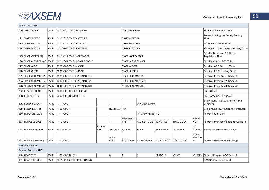
Register Bank Description 53
Packet Controller
220 TMGTXBOOST RW R 00110010 TMGTXBOOSTE TMGTXBOOSTM Transmit PLL Boost Time
221 TMGTXSETTLE RW R 00001010 TMGTXSETTLEE TMGTXSETTLEM Transmit PLL (post Boost) Settling Time
223 TMGRXBOOST RW R 00110010 TMGRXBOOSTE TMGRXBOOSTM Receive PLL Boost Time
224 TMGRXSETTLE RW R 00010100 TMGRXSETTLEE TMGRXSETTLEM Receive PLL (post Boost) Settling Time
225 TMGRXOFFSACQ RW R 01110011 TMGRXOFFSACQE TMGRXOFFSACQM Receive Baseband DC Offset Acquisition Time
226 TMGRXCOARSEAGC RW R 00111001 TMGRXCOARSEAGCE TMGRXCOARSEAGCM Receive Coarse AGC Time
227 TMGRXAGC RW R 00000000 TMGRXAGCE TMGRXAGCM Receiver AGC Settling Time
228 TMGRXRSSI RW R 00000000 TMGRXRSSIE TMGRXRSSIM Receiver RSSI Settling Time
229 TMGRXPREAMBLE1 RW R 00000000 TMGRXPREAMBLE1E TMGRXPREAMBLE1M Receiver Preamble 1 Timeout
22A TMGRXPREAMBLE2 RW R 00000000 TMGRXPREAMBLE2E TMGRXPREAMBLE2M Receiver Preamble 2 Timeout
22B TMGRXPREAMBLE3 RW R 00000000 TMGRXPREAMBLE3E TMGRXPREAMBLE3M Receiver Preamble 3 Timeout
22C RSSIREFERENCE RW R 00000000 RSSIREFERENCE RSSI Offset
22D RSSIABSTHR RW R 00000000 RSSIABSTHR RSSI Absolute Threshold
22E BGNDRSSIGAIN RW R ––––0000 – – – – BGNDRSSIGAIN Background RSSI Averaging Time Constant
22F BGNDRSSITHR RW R ––000000 – – BGNDRSSITHR Background RSSI Relative Threshold
230 PKTCHUNKSIZE RW R ––––0000 – – – – PKTCHUNKSIZE(3:0) Packet Chunk Size
231 PKTMISCFLAGS RW R –––00000 – – – WOR MULTI PKT AGC SETTL DET BGND RSSI RXAGC CLK
RXRSSI CLK Packet Controller Miscellaneous Flags
232 PKTSTOREFLAGS RW R –0000000 – ST ANT RSSI ST CRCB ST RSSI ST DR ST RFOFFS ST FOFFS
ST TIMER Packet Controller Store Flags
233 PKTACCEPTFLAGS RW R ––000000 – – ACCPT LRGP ACCPT SZF ACCPT ADDRF ACCPT CRCF ACCPT ABRT
ACCPT RESIDUE Packet Controller Accept Flags
Special Functions
General Purpose ADC
300 GPADCCTRL RW R ––000000 BUSY – 0 0 0 GPADC13 CONT CH ISOL General Purpose ADC Control
301 GPADCPERIOD RW R 00111111 GPADCPERIOD(7:0) GPADC Sampling Period
Version 1.10 Datasheet AX5043
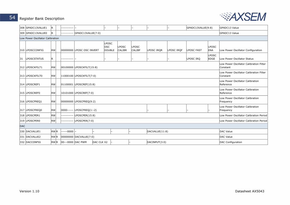
Register Bank Description 54
308 GPADC13VALUE1 R –––––––– – – – – – – GPADC13VALUE(9:8) GPADC13 Value
309 GPADC13VALUE0 R –––––––– GPADC13VALUE(7:0) GPADC13 Value
Low Power Oscillator Calibration
310 LPOSCCONFIG RW 00000000 LPOSC OSC INVERT
LPOSC OSC DOUBLE
LPOSC CALIBR
LPOSC CALIBF LPOSC IRQR LPOSC IRQF LPOSC FAST
LPOSC ENA Low Power Oscillator Configuration
31 LPOSCSTATUS R –––––––– – – – – – – LPOSC IRQ LPOSC EDGE Low Power Oscillator Status
312 LPOSCKFILT1 RW 00100000 LPOSCKFILT(15:8) Low Power Oscillator Calibration Filter Constant
313 LPOSCKFILT0 RW 11000100 LPOSCKFILT(7:0) Low Power Oscillator Calibration Filter Constant
314 LPOSCREF1 RW 01100001 LPOSCREF(15:8) Low Power Oscillator Calibration Reference
315 LPOSCREF0 RW 10101000 LPOSCREF(7:0) Low Power Oscillator Calibration Reference
316 LPOSCFREQ1 RW 00000000 LPOSCFREQ(9:2) Low Power Oscillator Calibration Frequency
317 LPOSCFREQ0 RW 0000–––– LPOSCFREQ(1:-2) – – – – Low Power Oscillator Calibration Frequency
318 LPOSCPER1 RW –––––––– LPOSCPER(15:8) Low Power Oscillator Calibration Period
319 LPOSCPER0 RW –––––––– LPOSCPER(7:0) Low Power Oscillator Calibration Period
DAC
330 DACVALUE1 RW R ––––0000 – – – – DACVALUE(11:8) DAC Value
331 DACVALUE2 RW R 00000000 DACVALUE(7:0) DAC Value
332 DACCONFIG RW R 00––0000 DAC PWM DAC CLK X2 – – DACINPUT(3:0) DAC Configuration
Version 1.10 Datasheet AX5043
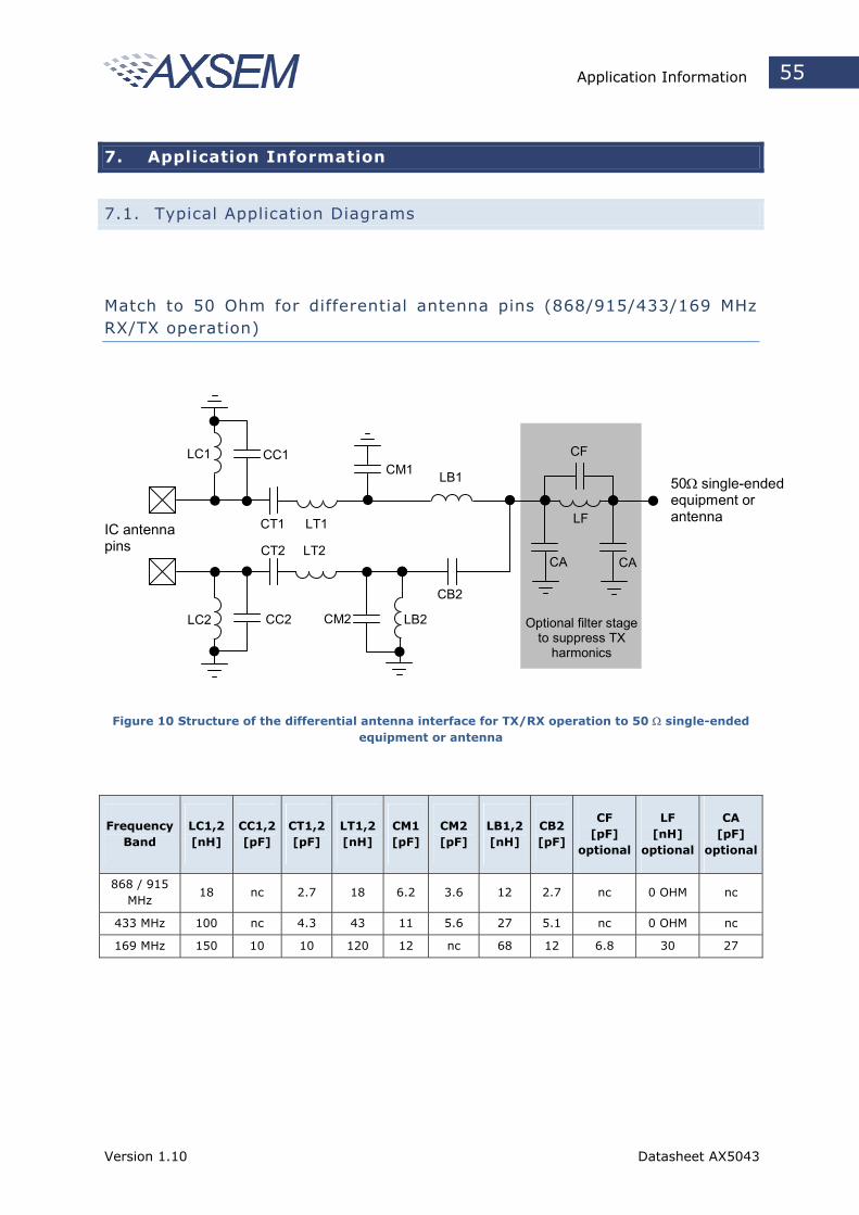
Application Information 55
7. Application Information
7.1. Typical Application Diagrams
Match to 50 Ohm for differential antenna pins (868/915/433/169 MHz RX/TX operation)
50Ω single-ended equipment or antenna
IC antenna pins
LT1
LC1
LB1
CT1
CC1 CM1
LT2
LC2
CT2
CC2 CM2
CB2
LB2
CF
LF
CA CA
Optional filter stage to suppress TX
harmonics
Figure 10 Structure of the differential antenna interface for TX/RX operation to 50 Ω single-ended equipment or antenna
Frequency Band
LC1,2 [nH]
CC1,2 [pF]
CT1,2 [pF]
LT1,2 [nH]
CM1 [pF]
CM2 [pF]
LB1,2 [nH]
CB2 [pF]
CF [pF]
optional
LF [nH]
optional
CA [pF]
optional
868 / 915 MHz
18 nc 2.7 18 6.2 3.6 12 2.7 nc 0 OHM nc
433 MHz 100 nc 4.3 43 11 5.6 27 5.1 nc 0 OHM nc
169 MHz 150 10 10 120 12 nc 68 12 6.8 30 27
Version 1.10 Datasheet AX5043
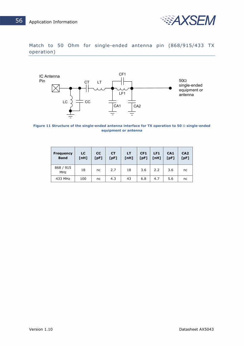
Application Information 56
Match to 50 Ohm for single-ended antenna pin (868/915/433 TX operation)
50Ω single-ended equipment or antenna
IC Antenna Pin LT
LC
CT
CC
CF1
LF1
CA1 CA2
Figure 11 Structure of the single-ended antenna interface for TX operation to 50 Ω single-ended equipment or antenna
Frequency Band
LC [nH]
CC [pF]
CT [pF]
LT [nH]
CF1 [pF]
LF1 [nH]
CA1 [pF]
CA2 [pF]
868 / 915 MHz
18 nc 2.7 18 3.6 2.2 3.6 nc
433 MHz 100 nc 4.3 43 6.8 4.7 5.6 nc
Version 1.10 Datasheet AX5043
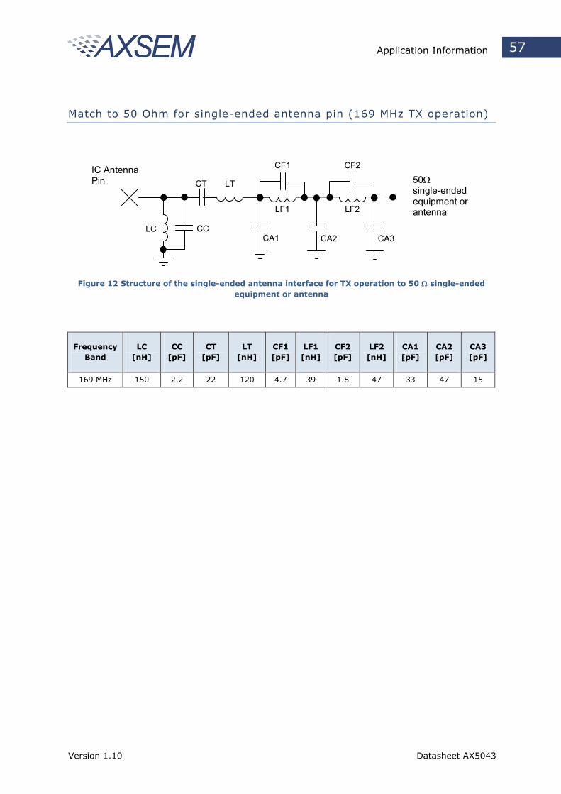
Application Information 57
Match to 50 Ohm for single-ended antenna pin (169 MHz TX operation)
50Ω single-ended equipment or antenna
IC Antenna Pin LT
LC
CT
CC
CF1
LF1
CA1 CA2
CF2
LF2
CA3
Figure 12 Structure of the single-ended antenna interface for TX operation to 50 Ω single-ended equipment or antenna
Frequency Band
LC [nH]
CC [pF]
CT [pF]
LT [nH]
CF1 [pF]
LF1 [nH]
CF2 [pF]
LF2 [nH]
CA1 [pF]
CA2 [pF]
CA3 [pF]
169 MHz 150 2.2 22 120 4.7 39 1.8 47 33 47 15
Version 1.10 Datasheet AX5043
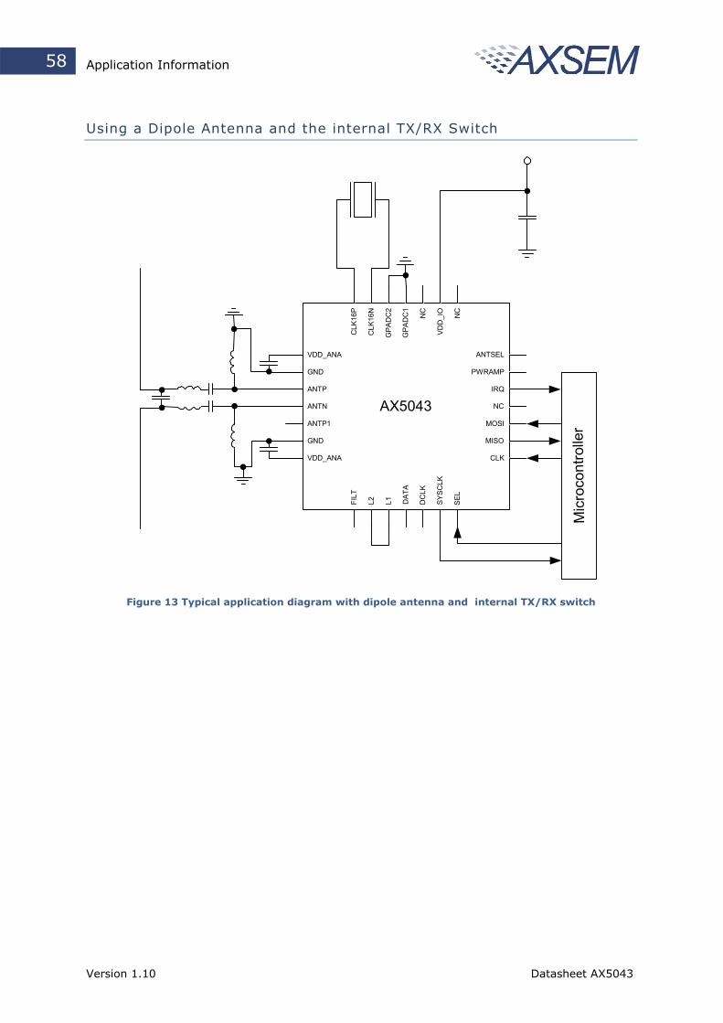
Application Information 58
Using a Dipole Antenna and the internal TX/RX Switch
VDD_ANA
GND
ANTP
ANTN
ANTP1
GND
VDD_ANA
CLK
16P
CLK
16N
GPA
DC
2
GPA
DC
1
NC
VDD
_IO NC
ANTSEL
PWRAMP
IRQ
NC
MOSI
MISO
CLK
FILT
L2 L1 DAT
A
SYSC
LK
SEL
DC
LK
Mic
roco
ntro
ller
AX5043
Figure 13 Typical application diagram with dipole antenna and internal TX/RX switch
Version 1.10 Datasheet AX5043
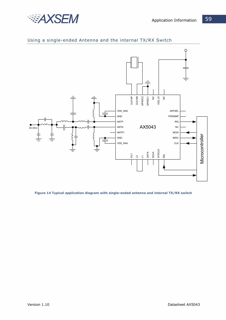
Application Information 59
Using a single-ended Antenna and the internal TX/RX Switch
VDD_ANA
GND
ANTP
ANTN
ANTP1
GND
VDD_ANA
CLK
16P
CLK
16N
GPA
DC
2
GPA
DC
1
NC
VDD
_IO NC
ANTSEL
PWRAMP
IRQ
NC
MOSI
MISO
CLK
FILT
L2 L1 DAT
A
SYSC
LK
SEL
DC
LK
Mic
roco
ntro
ller
AX504350 Ohm
Figure 14 Typical application diagram with single-ended antenna and internal TX/RX switch
Version 1.10 Datasheet AX5043
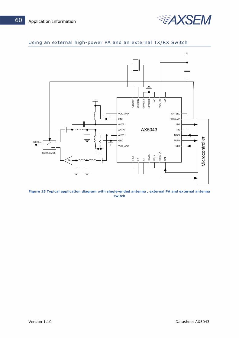
Application Information 60
Using an external high-power PA and an external TX/RX Switch
VDD_ANA
GND
ANTP
ANTN
ANTP1
GND
VDD_ANA
CLK
16P
CLK
16N
GPA
DC
2
GPA
DC
1
NC
VDD
_IO NC
ANTSEL
PWRAMP
IRQ
NC
MOSI
MISO
CLK
FILT
L2 L1 DAT
A
SYSC
LK
SEL
DC
LK
Mic
roco
ntro
ller
AX5043
50 Ohm
PA
TX/RX switch
Figure 15 Typical application diagram with single-ended antenna , external PA and external antenna switch
Version 1.10 Datasheet AX5043
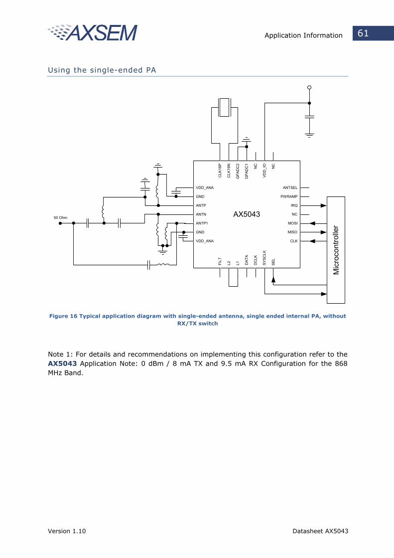
Application Information 61
Using the single-ended PA
VDD_ANA
GND
ANTP
ANTN
ANTP1
GND
VDD_ANA
CLK
16P
CLK
16N
GPA
DC
2
GPA
DC
1
NC
VDD
_IO NC
ANTSEL
PWRAMP
IRQ
NC
MOSI
MISO
CLK
FILT
L2 L1 DAT
A
SYSC
LK
SEL
DC
LK
Mic
roco
ntro
ller
AX504350 Ohm
Figure 16 Typical application diagram with single-ended antenna, single ended internal PA, without RX/TX switch
Note 1: For details and recommendations on implementing this configuration refer to the AX5043 Application Note: 0 dBm / 8 mA TX and 9.5 mA RX Configuration for the 868 MHz Band.
Version 1.10 Datasheet AX5043
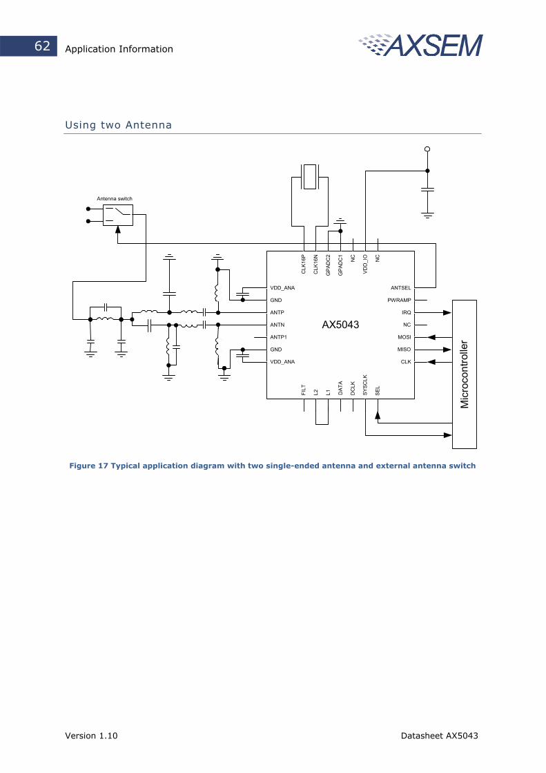
Application Information 62
Using two Antenna
VDD_ANA
GND
ANTP
ANTN
ANTP1
GND
VDD_ANA
CLK
16P
CLK
16N
GPA
DC
2
GPA
DC
1
NC
VDD
_IO NC
ANTSEL
PWRAMP
IRQ
NC
MOSI
MISO
CLK
FILT
L2 L1 DAT
A
SYSC
LK
SEL
DC
LK
Mic
roco
ntro
ller
AX5043
Antenna switch
Figure 17 Typical application diagram with two single-ended antenna and external antenna switch
Version 1.10 Datasheet AX5043
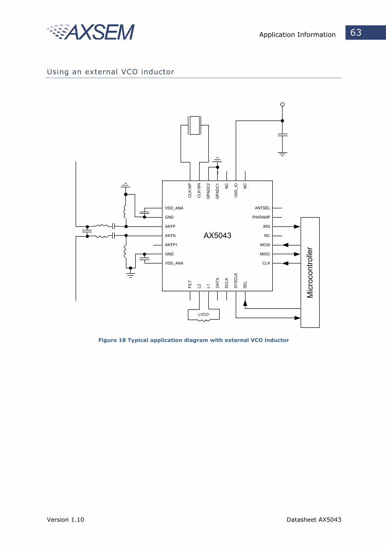
Application Information 63
Using an external VCO inductor
VDD_ANA
GND
ANTP
ANTN
ANTP1
GND
VDD_ANA
CLK
16P
CLK
16N
GPA
DC
2
GPA
DC
1
NC
VDD
_IO NC
ANTSEL
PWRAMP
IRQ
NC
MOSI
MISO
CLK
FILT
L2 L1 DAT
A
SYSC
LK
SEL
DC
LK
Mic
roco
ntro
ller
AX5043
LVCO
Figure 18 Typical application diagram with external VCO inductor
Version 1.10 Datasheet AX5043
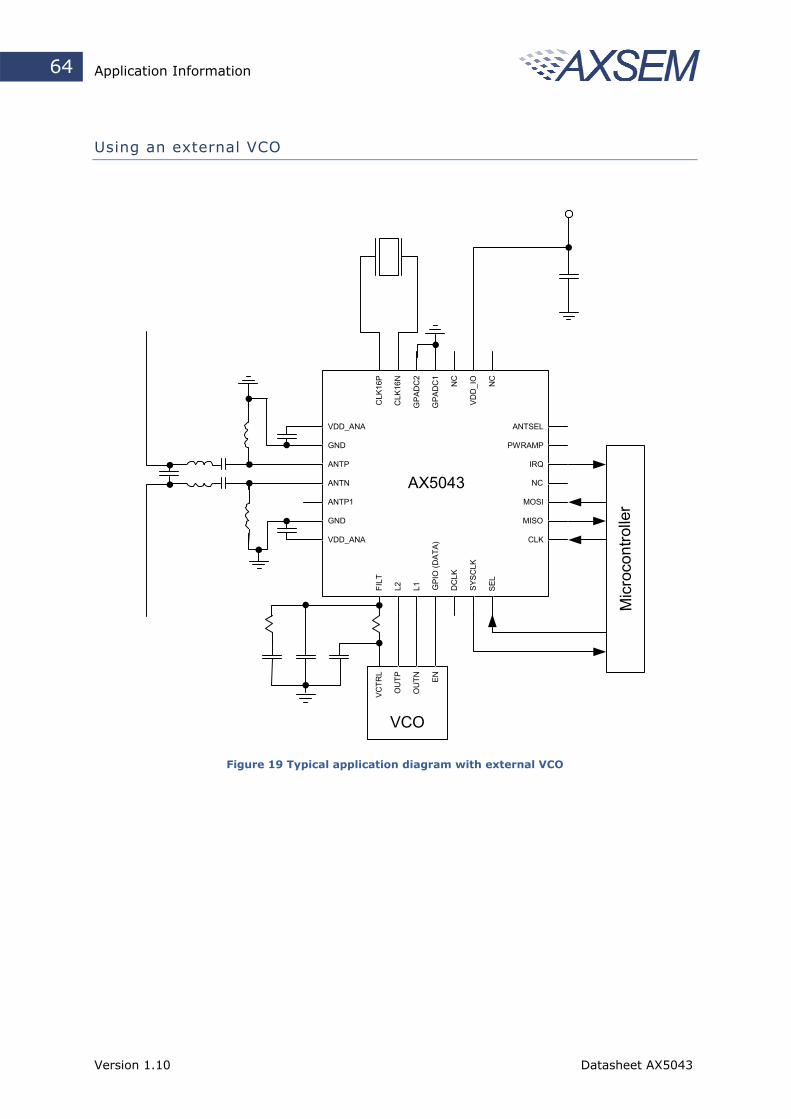
Application Information 64
Using an external VCO
VDD_ANA
GND
ANTP
ANTN
ANTP1
GND
VDD_ANA
CLK
16P
CLK
16N
GPA
DC
2
GPA
DC
1
NC
VD
D_I
O NC
ANTSEL
PWRAMP
IRQ
NC
MOSI
MISO
CLK
FILT
L2 L1 GPI
O (D
ATA)
SYSC
LK
SEL
DC
LK
Mic
roco
ntro
ller
AX5043
VCTR
L
OU
TP
OU
TN EN
VCO
Figure 19 Typical application diagram with external VCO
Version 1.10 Datasheet AX5043
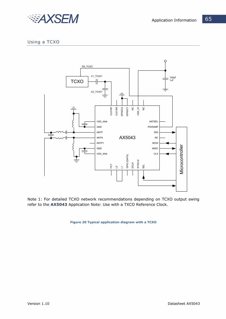
Application Information 65
Using a TCXO
VDD_ANA
GND
ANTP
ANTN
ANTP1
GND
VDD_ANA
CLK
16P
CLK
16N
GPA
DC
2
GPA
DC
1
NC
VDD
_IO NC
ANTSEL
PWRAMP
IRQ
NC
MOSI
MISO
CLK
FILT
L2 L1 GPI
O (D
ATA)
SYSC
LK
SEL
DC
LK
Mic
roco
ntro
ller
AX5043
100pF1uFTCXO
C1_TCXO1
C2_TCXO1
EN_TCXO
Note 1: For detailed TCXO network recommendations depending on TCXO output swing refer to the AX5043 Application Note: Use with a TXCO Reference Clock.
Figure 20 Typical application diagram with a TCXO
Version 1.10 Datasheet AX5043
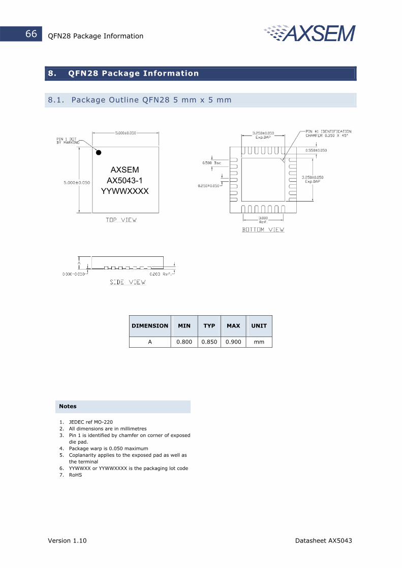
QFN28 Package Information 66
8. QFN28 Package Information
8.1. Package Outline QFN28 5 mm x 5 mm
AXSEM AX5043-1
YYWWXXXX
DIMENSION MIN TYP MAX UNIT
A 0.800 0.850 0.900 mm
Ve
Notes
1. JEDEC ref MO-220 2. All dimensions are in millimetres 3. Pin 1 is identified by chamfer on corner of exposed
die pad. 4. Package warp is 0.050 maximum 5. Coplanarity applies to the exposed pad as well as
the terminal 6. YYWWXX or YYWWXXXX is the packaging lot code 7. RoHS
rsion 1.10 Datasheet AX5043
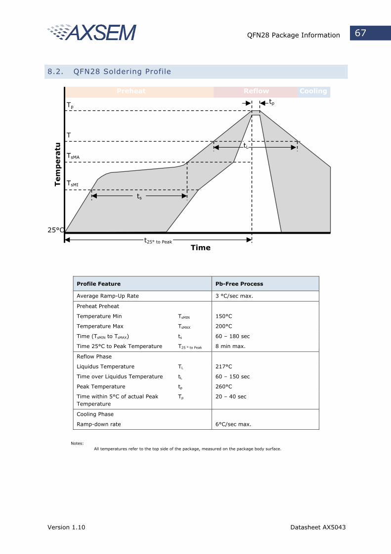
QFN28 Package Information 67
8.2. QFN28 Soldering Profile
Profile Feature Pb-Free Process
Average Ramp-Up Rate 3 °C/sec max.
Preheat Preheat
Temperature Min TsMIN 150°C
Temperature Max TsMAX 200°C
Time (TsMIN to TsMAX) ts 60 – 180 sec
Time 25°C to Peak Temperature T25 ° to Peak 8 min max.
Reflow Phase
Liquidus Temperature TL 217°C
Time over Liquidus Temperature tL 60 – 150 sec
Peak Temperature tp 260°C
Time within 5°C of actual Peak Temperature
Tp 20 – 40 sec
Cooling Phase
Ramp-down rate 6°C/sec max.
Notes: All temperatures refer to the top side of the package, measured on the package body surface.
Time
Preheat Reflow Cooling
Tp
T
TsMA
TsMI
tp
25°C
ts
tL
t25° to Peak
Tem
pera
tu
Version 1.10 Datasheet AX5043
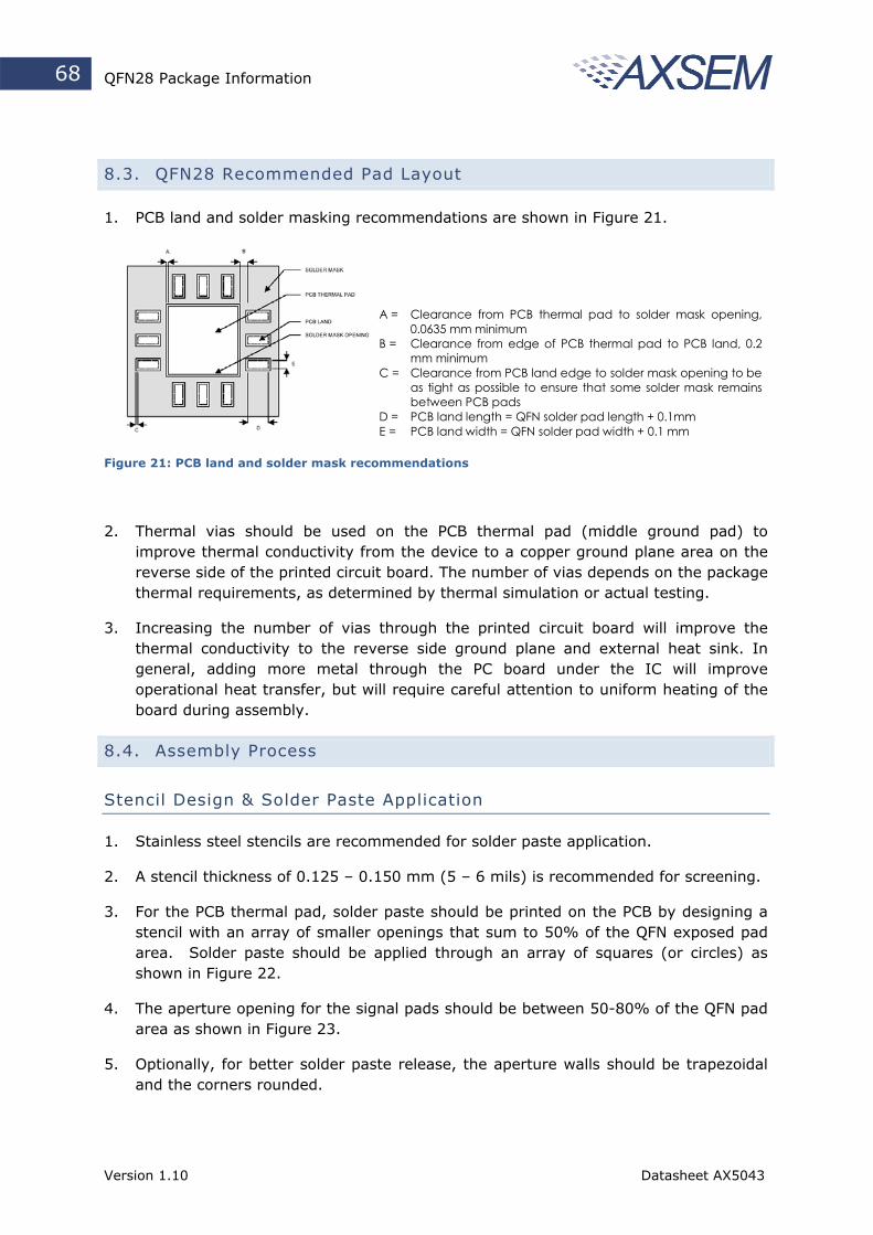
QFN28 Package Information 68
8.3. QFN28 Recommended Pad Layout
1. PCB land and solder masking recommendations are shown in Figure 21.
A = Clearance from PCB thermal pad to solder mask opening,0.0635 mm minimum
B = Clearance from edge of PCB thermal pad to PCB land, 0.2mm minimum
C = Clearance from PCB land edge to solder mask opening to beas tight as possible to ensure that some solder mask remainsbetween PCB pads
D = PCB land length = QFN solder pad length + 0.1mm E = PCB land width = QFN solder pad width + 0.1 mm
Figure 21: PCB land and solder mask recommendations
2. Thermal vias should be used on the PCB thermal pad (middle ground pad) to improve thermal conductivity from the device to a copper ground plane area on the reverse side of the printed circuit board. The number of vias depends on the package thermal requirements, as determined by thermal simulation or actual testing.
3. Increasing the number of vias through the printed circuit board will improve the thermal conductivity to the reverse side ground plane and external heat sink. In general, adding more metal through the PC board under the IC will improve operational heat transfer, but will require careful attention to uniform heating of the board during assembly.
8.4. Assembly Process
Stencil Design & Solder Paste Application
1. Stainless steel stencils are recommended for solder paste application.
2. A stencil thickness of 0.125 – 0.150 mm (5 – 6 mils) is recommended for screening.
3. For the PCB thermal pad, solder paste should be printed on the PCB by designing a stencil with an array of smaller openings that sum to 50% of the QFN exposed pad area. Solder paste should be applied through an array of squares (or circles) as shown in Figure 22.
4. The aperture opening for the signal pads should be between 50-80% of the QFN pad area as shown in Figure 23.
5. Optionally, for better solder paste release, the aperture walls should be trapezoidal and the corners rounded.
Version 1.10 Datasheet AX5043
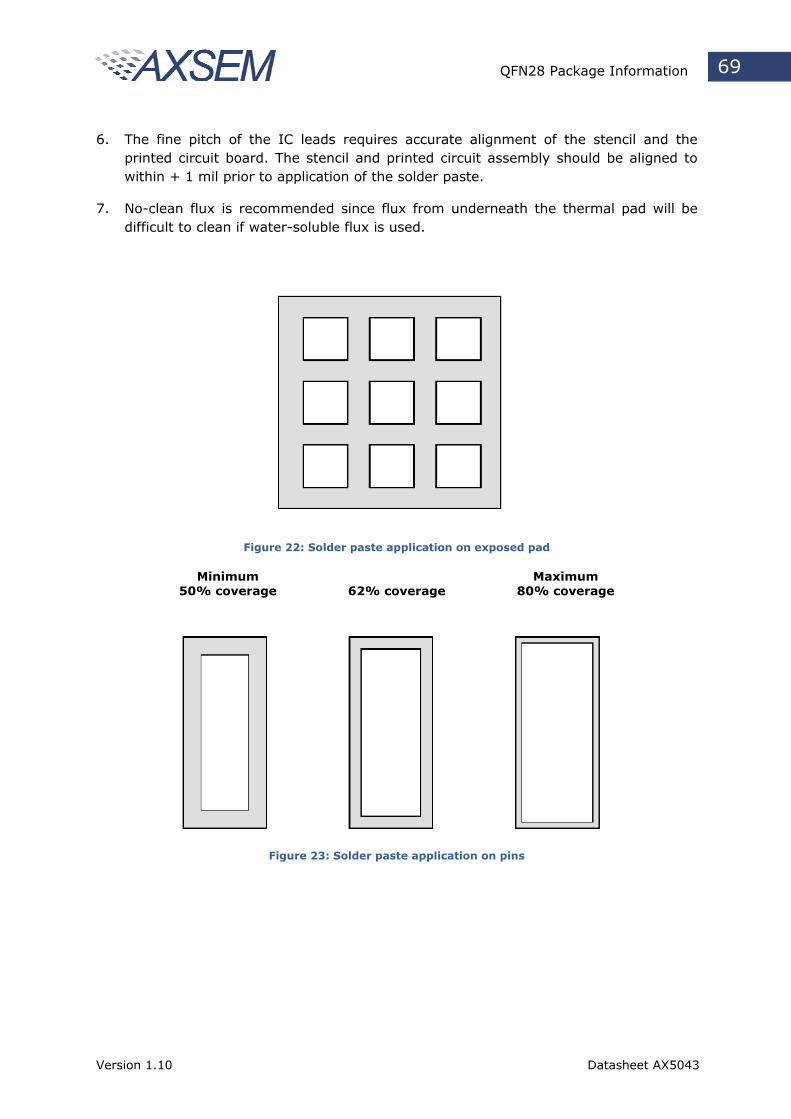
QFN28 Package Information 69
6. The fine pitch of the IC leads requires accurate alignment of the stencil and the printed circuit board. The stencil and printed circuit assembly should be aligned to within + 1 mil prior to application of the solder paste.
7. No-clean flux is recommended since flux from underneath the thermal pad will be difficult to clean if water-soluble flux is used.
Figure 22: Solder paste application on exposed pad
Minimum 50% coverage
62% coverage
Maximum 80% coverage
Figure 23: Solder paste application on pins
Version 1.10 Datasheet AX5043
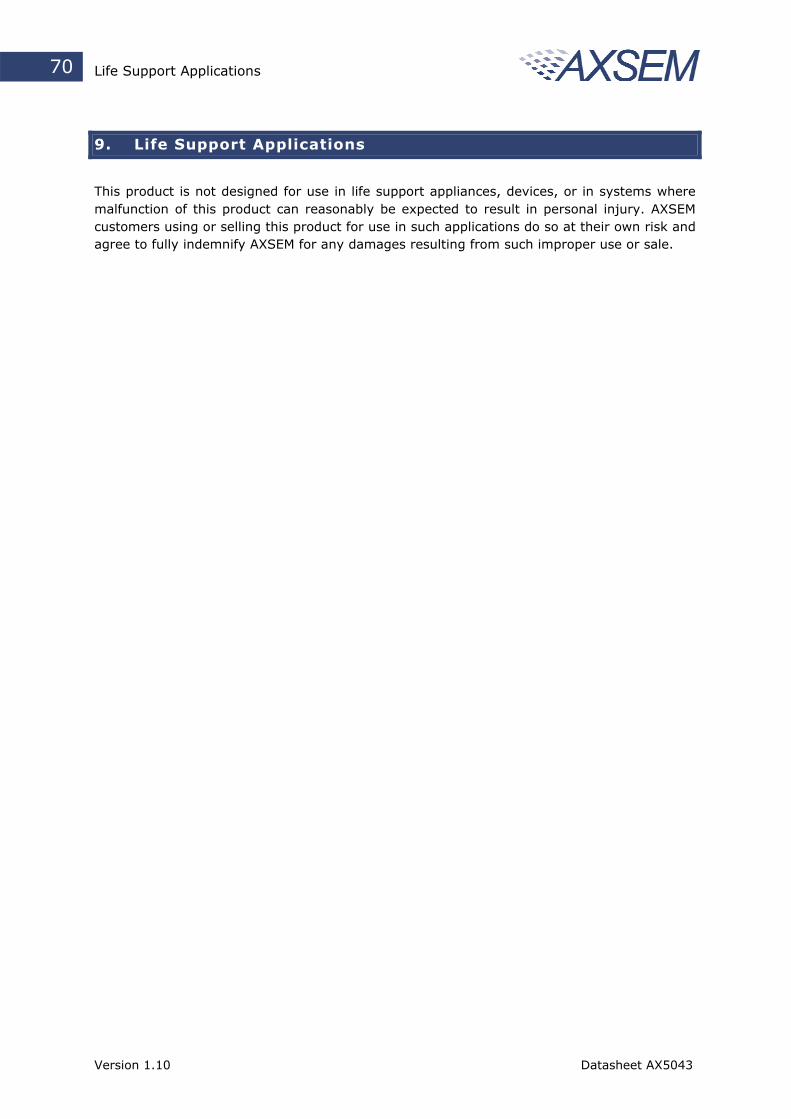
Life Support Applications 70
9. Life Support Applications
This product is not designed for use in life support appliances, devices, or in systems where malfunction of this product can reasonably be expected to result in personal injury. AXSEM customers using or selling this product for use in such applications do so at their own risk and agree to fully indemnify AXSEM for any damages resulting from such improper use or sale.
Version 1.10 Datasheet AX5043
Contact Information 71
10. Contact Information
AXSEM AG Oskar-Bider-Strasse 1 CH-8600 Dübendorf SWITZERLAND
Phone +41 44 882 17 07 Fax +41 44 882 17 09 Email [email protected] www.axsem.com
For further product related or sales information please visit our website or contact your local representative.
The specifications in this document are subject to change at AXSEM's discretion. AXSEM assumes no responsibility for any claims or damages arising out of the use of thisdocument, or from the use of products based on this document, including but not limited to claims or damages based on infringement of patents, copyrights or other intellectualproperty rights. AXSEM makes no warranties, either expressed or implied with respect to the information and specifications contained in this document. AXSEM does not supportany applications in connection with life support and commercial aircraft. Performance characteristics listed in this document are estimates only and do not constitute a warranty orguarantee of product performance. The copying, distribution and utilization of this document as well as the communication of its contents to others without expressed authorizationis prohibited. Offenders will be held liable for the payment of damages. All rights reserved. Copyright © 2010-2014 AXSEM AG
Version 1.10 Datasheet AX5043