Embed Size (px)
Citation preview
Copyright© 2016 ARM Limited. All Rights Reserved
ARM DUI 0998B
SoC Designer Version 8.4
AXIv2 Protocol Bundle User Guide
Non-Confidential
ARM DUI 0998B Copyright© 2016 ARM Limited. All Rights Reserved 2
Non-Confidential
SoC Designer AXIv2 Protocol Bundle User Guide
Copyright © 2016 ARM Limited. All rights reserved.
Release Information
The following changes have been made to this document.
Change History
Date Issue Confidentiality Change
March 2016 A Non-Confidential Restamp Release
with 8.4
Non-Confidential Proprietary Notice
This document is protected by copyright and other related rights and the practice or implementation of the information contained in
this document may be protected by one or more patents or pending patent applications. No part of this document may be reproduced in
any form by any means without the express prior written permission of ARM Limited (“ARM”). No license, express or implied, by
estoppel or otherwise to any intellectual property rights is granted by this document unless specifically stated.
Your access to the information in this document is conditional upon your acceptance that you will not use or permit others to use the
information for the purposes of determining whether implementations infringe any patents.
THIS DOCUMENT IS PROVIDED “AS IS”. ARM PROVIDES NO REPRESENTATIONS AND NO WARRANTIES, EXPRESS,
IMPLIED OR STATUTORY, INCLUDING, WITHOUT LIMITATION, THE IMPLIED WARRANTIES OF
MERCHANTABILITY, SATISFACTORY QUALITY, NON-INFRINGEMENT OR FITNESS FOR A PARTICULAR PURPOSE
WITH RESPECT TO THE DOCUMENT. For the avoidance of doubt, ARM makes no representation with respect to, and has
undertaken no analysis to identify or understand the scope and content of, third party patents, copyrights, trade secrets, or other rights.
This document may include technical inaccuracies or typographical errors.
This document may be translated into other languages for convenience, and you agree that if there is any conflict between the English
version of this document and any translation, the terms of the English version shall prevail.
TO THE EXTENT NOT PROHIBITED BY LAW, IN NO EVENT WILL ARM BE LIABLE FOR ANY DAMAGES, INCLUDING
WITHOUT LIMITATION ANY DIRECT, INDIRECT, SPECIAL, INCIDENTAL, PUNITIVE, OR CONSEQUENTIAL
DAMAGES, HOWEVER CAUSED AND REGARDLESS OF THE THEORY OF LIABILITY, ARISING OUT OF ANY USE OF
THIS DOCUMENT, EVEN IF ARM HAS BEEN ADVISED OF THE POSSIBILITY OF SUCH DAMAGES.
This document consists solely of commercial items. You shall be responsible for ensuring that any use, duplication or disclosure of
this document complies fully with any relevant export laws and regulations to assure that this document or any portion thereof is not
exported, directly or indirectly, in violation of such export laws. Use of the word “partner” in reference to ARM’s customers is not
intended to create or refer to any partnership relationship with any other company. ARM may make changes to this document at any
time and without notice.
If any of the provisions contained in these terms conflict with any of the provisions of any signed written agreement specifically
covering this document with ARM, then the signed written agreement prevails over and supersedes the conflicting provisions of these
terms.
Words and logos marked with ® or ™ are registered trademarks or trademarks of ARM Limited or its affiliates in the EU and/or
elsewhere. All rights reserved. Other brands and names mentioned in this document may be the trademarks of their respective owners.
You must follow the ARM trademark usage guidelines http://www.arm.com/about/trademarks/guidelines/index.php.
Copyright © ARM Limited or its affiliates. All rights reserved.
ARM Limited. Company 02557590 registered in England.
110 Fulbourn Road, Cambridge, England CB1 9NJ.
In this document, where the term ARM is used to refer to the company it means “ARM or any of its subsidiaries as appropriate”.

ARM DUI 0998B Copyright© 2016 ARM Limited. All Rights Reserved 3
Non-Confidential
Confidentiality Status
This document is Non-Confidential. The right to use, copy and disclose this document may be subject to license restrictions in
accordance with the terms of the agreement entered into by ARM and the party that ARM delivered this document to.
Product Status
The information in this document is final, that is for a developed product.
Web Address
http://www.arm.com
ARM DUI 0998B Copyright© 2016 ARM Limited. All Rights Reserved 4
Non-Confidential
Table of Contents
1 Introduction ............................................................................................ 6
2 Requirements .......................................................................................... 6
3 Bundle Contents ...................................................................................... 6
3.1 AXIv2 Models and Examples .............................................................................. 6
3.2 AXIv2 Probes ....................................................................................................... 6
3.3 AXIv2 Ports.......................................................................................................... 6
3.4 AXIv2 Component Wizard Templates ................................................................. 7
4 Models ...................................................................................................... 7
4.1 AXIv2_Master ...................................................................................................... 9
4.2 AXIv2_Slave ...................................................................................................... 10
4.3 AXIv2_Mem ...................................................................................................... 11
4.4 AXIv2_Stub ....................................................................................................... 13
4.4.1 AXIv2_Stub Macros ................................................................................... 13
4.5 AxiToAxi2 ......................................................................................................... 14
4.6 Axi2ToAxi ......................................................................................................... 14
4.7 MxAXIv2 ........................................................................................................... 16
4.8 AXIv2PassThrough ............................................................................................ 17
4.9 Example System ................................................................................................. 18
4.10 Disk Backed Memory Functionality .................................................................. 19
Disk Backed Memory Use Case ................................................................................ 20
5 Probes..................................................................................................... 21
5.1 Tracer ................................................................................................................. 22
5.2 Breakpoint .......................................................................................................... 23
5.3 Profiling .............................................................................................................. 23
ARM DUI 0998B Copyright© 2016 ARM Limited. All Rights Reserved 5
Non-Confidential
5.4 Monitor ............................................................................................................... 24
6 Component Wizard .............................................................................. 25
6.1 Generating AXIv2 Ports ..................................................................................... 25
7 AXIv2 Port Interfaces .......................................................................... 26
7.1 Port Classes ........................................................................................................ 26
7.2 Channel Ports ..................................................................................................... 26
7.3 Master Interface.................................................................................................. 28
7.3.1 AXI_Master_Port ........................................................................................ 28
7.3.2 AXI Sender and Receiver Ports for AXI Master Interface ......................... 29
7.3.3 Methods for Setting Channel Signal Values ............................................... 29
7.3.4 sendDrive .................................................................................................... 30
7.3.5 Initialization and Reset ............................................................................... 30
7.3.6 Supporting Combinatorial Ready-On-Valid ............................................... 30
7.4 Slave Interface .................................................................................................... 31
7.4.1 AXI_Slave_Port .......................................................................................... 31
7.4.2 AXI Sender and Receiver Ports for AXI Slave Interface ........................... 31
7.4.3 Methods for Setting Channel Signal Values ............................................... 32
7.4.4 sendDrive .................................................................................................... 32
7.4.5 Initialization and Reset ............................................................................... 32
7.5 Note on using large AXI ID widths ................................................................... 32
7.6 Examples ............................................................................................................ 33
7.6.1 AXI Master ................................................................................................. 33
7.6.1.1 AXI Master Port ...................................................................................... 33
7.6.1.2 AXI Master Component .......................................................................... 33
7.6.2 AXI Slave.................................................................................................... 34
7.6.2.1 AXI Slave Port ........................................................................................ 34
7.6.2.2 AXI Slave Component ............................................................................ 35
8 Appendix: Example of altering AxiV2PassThrough for ARM Cortex-A9 and
ARM PL310 support for Lockdown by Master feature. ...................................... 36

ARM DUI 0998B Copyright© 2016 ARM Limited. All Rights Reserved 6
Non-Confidential
1 Introduction
This is the user guide for the SoC Designer AXIv2 Protocol Bundle. This protocol bundle
contains SoC Designer components, probes, and the transaction port interfaces for the
SoC Designer CASI Transaction Level Modeling (TLM) version 2 of the ARM AMBA3 AXI
protocol.
AXI TLMv2 introduces two major fundamental changes that distinguish it from the previous
version of the CASI AXI TLM definition:
Control granularity at the AXI channel level
Signal-level communication
The first aspect is important as both the transaction master and the slave can be initiators on the
AXI channels. This is essential to supporting combinatorial paths, as will be described later in
this manual.
Signal-level communication is introduced mainly to reduce the burden on the model developer
and to promote hardware-accurate modeling: modeling the signals closely as represented in
hardware eliminates the need to keep track of the transaction level viewpoint. The model
developer is only required to model the hardware signals, and the rest of the task is left for the
tool (SoC Designer) to construct the transaction views on top of the signal communication.
2 Requirements
The AXIv2 protocol bundle requires the following:
SoC Designer version 8.4 or later.
Compilation tools as set forth in the SoC Designer Installation Guide.
3 Bundle Contents
This bundle contains a full release of the CASI AXIv2 protocol, which is an enhanced version of
the previous interface which had a limitation in handling asynchronous AXI transfers. The
AXIv2 protocol bundle contains the following components.
3.1 AXIv2 Models and Examples
Generic components such as configurable bus and memory are included in this bundle. Also
provided is example source code to help users develop custom AXI components:
3.2 AXIv2 Probes
Probes provide visibility into transactions between two components. AXIv2 specific probes are
included in this protocol bundle.
3.3 AXIv2 Ports
AXIv2 transaction port definition header files and libraries are included in this package. These
are required during runtime of any components with AXIv2 ports and also when creating
components with AXIv2 ports.

ARM DUI 0998B Copyright© 2016 ARM Limited. All Rights Reserved 7
Non-Confidential
3.4 AXIv2 Component Wizard Templates
The AXIv2 protocol bundle includes the template files needed by the SoC Designer Component
Wizard for generation of components with AXIv2 ports.
Note on Asynchronous Clock Domains
Support for asynchronous clock domains is limited to native AXIv2 components only. This
means that an AXIv1 master does not function correctly if connected to an AXIv2 slave
(through an AxiToAxi2 bridge) in an asynchronous clocking scheme. There are no known
issues with synchronous clocking schemes (for example, clocking which requires AXI
SyncUp or SyncDn only) and AXIv1 components; however, this is not a guarantee that all
AXIv1 components will work in this fashion. It is recommended to try to avoid the use of
AXI TLM bridges (i.e., AxiToAxi2 and Axi2ToAxi) wherever possible.
4 Models
The following table lists the AXIv2 components included in this bundle.
Component Description
AXIv2_Master This is an example AXIv2 master component.
AXIv2_Slave This is an example AXIv2 slave component.
AXIv2_Mem A generic AXIv2 memory component with an AXIv2 interface.
AXIv2_Stub A scriptable AXIv2 master component.
AxiToAxi2 This is a TLM adaptor that bridges an AXIv1 master port to an AXIv2
slave port.
Axi2ToAxi This is a TLM adaptor that bridges an AXIv2 master port to an AXIv1
slave port.
MxAXIv2 A generic AXI interconnect model supporting up to 16 masters and 16
slaves.
AXIv2PassThrough This is a component that allows AXI transactions to “passthrough” the
component. By altering the source code, users may enable additional
features such as Lockdown by Master between the ARM Cortex-A9 and
the ARM PL310 L2 Cache Controller.
Table 4-1 AXIv2 Components
The following components are not part of the AXIv2 bundle. However, you should be aware of
them if you are implementing AXI4.
Note: These components are bundled with the AXI4 Protocol Bundle. For more information,
refer to the AXI4 Protocol Bundle User Guide.
ARM DUI 0998B Copyright© 2016 ARM Limited. All Rights Reserved 8
Non-Confidential
AXI4ToAXIv2 Bridges an AXI4 master component to an AXIv2 slave component.
AXIv2ToAXI4 Bridges an AXIv2 master component to an AXI4 slave component.
Table 4-2 Additional AXIv2-related Components
The .conf file for AXIv2 components is located under the $MAXSIM_PROTOCOLS\AXIv2\etc
directory.
Note: The TLM adaptors will not improve accuracy over the original AXI TLM. These adaptors
are provided as a migration path only. User custom components should be updated to use
the new TLM to attain true accuracy.

ARM DUI 0998B Copyright© 2016 ARM Limited. All Rights Reserved 9
Non-Confidential
4.1 AXIv2_Master
AXIv2 _Master is an example AXI component using AXI TLMv2 master port. This component
alternates issuing read and write transactions. Address and Data bit-widths are configurable, as
well as delays on the R and B ready handshake signals.
There is an example system which uses AXIv2 _Master located in
$MAXSIM_PROTOCOLS/AXIv2/examples/MasterSlave.
This example component is provided in source code form under
$MAXSIM_PROTOCOLS/src/AXIv2_Master.
Figure 4-1 AXIv2_Master
The table below lists the component parameters.
Name Description
Address Width Width in bits of the address bus. Supported range is 1 to 64. Settable
at sdcanvas time only; not settable at runtime.
B ready delay Number of delay cycles for the B channel ready response.
Data Width Width in bits of the data bus. It must match the data bus width of the
connected model. Allowed values are 32, 64, and 128.
Enable If false, the component will not generate any transactions.
Enable aw & w
simultaneous
Used to enable the AW and W channels at the same time. Usually W
follows AW, but you can change this parameter so that both channels
go high at the same time.
Enable Debug
Messages
When set to true, the model debug messages are displayed as output.
Enable multiple reads If true, the component will try to issue a second read transaction
even if the first read transaction has not completed.
Enable output Enable printing of informational messages about transactions in a
SoC Designer Console window.
R ready delay Number of delay cycles for the R channel ready response.
Start address The starting address of transactions. Address will be incremented by
the data width for each transaction.
Start address2 Specifies the address for the second read transaction in case Enable
multiple reads is set to true.
Start with writes If true, the component will issue a write as the first transaction. If
false, the component will issue a read as the first transaction.
Table 4-2 AXIv2_Master Parameters
ARM DUI 0998B Copyright© 2016 ARM Limited. All Rights Reserved 10
Non-Confidential
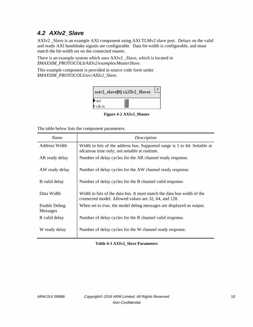
4.2 AXIv2_Slave
AXIv2 _Slave is an example AXI component using AXI TLMv2 slave port. Delays on the valid
and ready AXI handshake signals are configurable. Data bit-width is configurable, and must
match the bit-width set on the connected master.
There is an example system which uses AXIv2 _Slave, which is located in
$MAXSIM_PROTOCOLS/AXIv2/examples/MasterSlave.
This example component is provided in source code form under
$MAXSIM_PROTOCOLS/src/AXIv2_Slave.
Figure 4-2 AXIv2_Master
The table below lists the component parameters.
Name Description
Address Width Width in bits of the address bus. Supported range is 1 to 64. Settable at
sdcanvas time only; not settable at runtime.
AR ready delay Number of delay cycles for the AR channel ready response.
AW ready delay Number of delay cycles for the AW channel ready response.
B valid delay Number of delay cycles for the B channel valid response.
Data Width Width in bits of the data bus. It must match the data bus width of the
connected model. Allowed values are 32, 64, and 128.
Enable Debug
Messages
When set to true, the model debug messages are displayed as output.
R valid delay Number of delay cycles for the R channel valid response.
W ready delay Number of delay cycles for the W channel ready response.
Table 4-3 AXIv2_Slave Parameters
ARM DUI 0998B Copyright© 2016 ARM Limited. All Rights Reserved 11
Non-Confidential
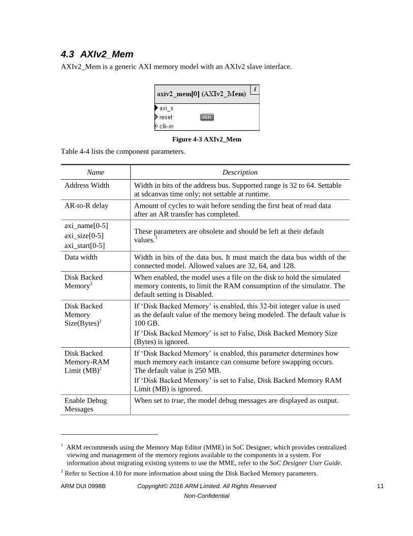
4.3 AXIv2_Mem
AXIv2_Mem is a generic AXI memory model with an AXIv2 slave interface.
Figure 4-3 AXIv2_Mem
Table 4-4 lists the component parameters.
Name Description
Address Width Width in bits of the address bus. Supported range is 32 to 64. Settable
at sdcanvas time only; not settable at runtime.
AR-to-R delay Amount of cycles to wait before sending the first beat of read data
after an AR transfer has completed.
axi_name[0-5]
axi_size[0-5]
axi_start[0-5]
These parameters are obsolete and should be left at their default
values.1
Data width Width in bits of the data bus. It must match the data bus width of the
connected model. Allowed values are 32, 64, and 128.
Disk Backed
Memory2
When enabled, the model uses a file on the disk to hold the simulated
memory contents, to limit the RAM consumption of the simulator. The
default setting is Disabled.
Disk Backed
Memory
Size(Bytes)2
If ‘Disk Backed Memory’ is enabled, this 32-bit integer value is used
as the default value of the memory being modeled. The default value is
100 GB.
If ‘Disk Backed Memory’ is set to False, Disk Backed Memory Size
(Bytes) is ignored.
Disk Backed
Memory-RAM
Limit (MB)2
If ‘Disk Backed Memory’ is enabled, this parameter determines how
much memory each instance can consume before swapping occurs.
The default value is 250 MB.
If ‘Disk Backed Memory’ is set to False, Disk Backed Memory RAM
Limit (MB) is ignored.
Enable Debug
Messages
When set to true, the model debug messages are displayed as output.
1 ARM recommends using the Memory Map Editor (MME) in SoC Designer, which provides centralized
viewing and management of the memory regions available to the components in a system. For
information about migrating existing systems to use the MME, refer to the SoC Designer User Guide. 2 Refer to Section 4.10 for more information about using the Disk Backed Memory parameters.
ARM DUI 0998B Copyright© 2016 ARM Limited. All Rights Reserved 12
Non-Confidential
Enable Warnings When set to true, this parameter enables printing of warning messages.
Exclusive Monitor When set to true (the default setting), the memory does additional
checking for exclusive access requests and can return EXOKAY for
success on RRESP or BRESP. When set to false, exclusive access
requests always return OKAY, which is a failure code. Only the true
value allows the memory to be fully compliant with the AMBA AXI
and ACE specification.
Num of Exclusive
Monitors
The maximum number of exclusive monitors needed. This parameter
becomes active only when the Exclusive Monitor parameter is set to
true. If this value is set to 0 when Exclusive Monitor= true, the
exclusive monitor is not turned on.
RAM Usage Limit
(MB)
If ‘Disk backed memory’ is set to true, this integer value will set the
threshold for the memory model on the RAM consumption before
starting to swap its contents to the file.
If ‘Disk backed memory’ is set to false, it will be Ignored.
WS Read The number of wait cycles introduced for a Read access is given by
this parameter.
WS Write The number of wait cycles introduced for a Write access is given by
this parameter.
W-to-B delay Number of cycles to wait before sending the B response after the Write
data transfer has completed
Table 4-4 AXIv2_Mem Parameters

ARM DUI 0998B Copyright© 2016 ARM Limited. All Rights Reserved 13
Non-Confidential
4.4 AXIv2_Stub
AXIv2_Stub is an AXIv2 master component which can be controlled with a SoC Designer mxscr
script.
Figure 4-5 AXIv2_Stub
Note: On stub components, accessing transaction slave ports using MxScript is not supported.
Use a memory component if scripting is required.
The table below lists the component parameters.
Name Description
Address Width Width in bits of the address bus. Supported range is 8 to 63. Settable at
sdcanvas time only; not settable at runtime.
axi_name[0-5]
axi_size[0-5]
axi_start[0-5]
These parameters are obsolete and should be left at their default values.3
CPP include path Additional include path for header files to be used by script
preprocessor.
Data Width Width in bits of the data bus. It must match the data bus width of the
connected model. Allowed values are 32, 64, and 128.
Enable Debug
Messages
When set to true, the model debug messages are displayed as output.
Memory Init Byte
Value
The initial value used for each byte of the memory.
Table 4-5 AXIv2_Stub Parameters
4.4.1 AXIv2_Stub Macros
Macro definitions for AXIv2_Stub are provided in the following files:
3 ARM recommends using the Memory Map Editor (MME) in SoC Designer, which provides centralized
viewing and management of the memory regions available to the components in a system. For
information about migrating existing systems to use the MME, refer to the SoC Designer User Guide.
ARM DUI 0998B Copyright© 2016 ARM Limited. All Rights Reserved 14
Non-Confidential
- $MAXSIM_PROTOCOLS/AXIv2/include/AXIv2_Stub_Macros.h
- $MAXSIM_ PROTOCOLS/AXIv2/include/AXIv2_Stub_CheckMacros.h
For information about how to use the macros, read the comments in the .h files.
4.5 AxiToAxi2
This component bridges an AXIv1 master port to an AXIv2 slave port. AXI signals that only
exist in the v2 interface are assumed to be tied to zero when going through this bridge.
Figure 4-64 AxiToAxi2
The table below lists the component parameters.
Name Description
Address width Width in bits of the address bus. Supported range is 32 to 64. Settable
at sdcanvas time only; not settable at runtime.
axi_name[0-5]
axi_size[0-5]
axi_start[0-5]
These parameters are obsolete and should be left at their default
values.4
Data width Width in bits of the data bus. It must match the data bus width of the
connected model. Allowed values are 32, 64, and 128.
Enable debug
messages
When set to true, the model debug messages are displayed as output.
Forward address
regions
If true, the adaptor will forward address regions reported by the
connected slave to the connected master.
Skip redundant
transactions
If true, the adaptor will avoid resending redundant transactions in the
same cycle. If true, it may provide speed improvements.
Table 4-6 AxiToAxi2 Parameters
4.6 Axi2ToAxi
This component bridges an AXIv2 master port to an AXIv1 slave port. AXI signals that only
exist in the v2 interface are assumed to be tied to zero when going through this bridge.
4 ARM recommends using the Memory Map Editor (MME) in SoC Designer, which provides centralized
viewing and management of the memory regions available to the components in a system. For
information about migrating existing systems to use the MME, refer to the SoC Designer User Guide.
ARM DUI 0998B Copyright© 2016 ARM Limited. All Rights Reserved 15
Non-Confidential
Figure 4-7 Axi2ToAxi
The table below lists the component parameters.
Name Description
Address width Width in bits of the address bus. Supported range is 32 to 64.
Settable at sdcanvas time only; not settable at runtime.
axi_name[0-5]
axi_size[0-5]
axi_start[0-5]
These parameters are obsolete and should be left at their default
values.5
Data width Width in bits of the data bus. It must match the data bus width of the
connected model. Allowed values are 32, 64, and 128.
Enable debug
messages
When set to true, the model debug messages are displayed as output.
Forward address
regions
If true, the adaptor will forward address regions reported by the
connected slave to the connected master.
Skip redundant
transactions
If true, the adaptor will avoid resending redundant transactions in the
same cycle. If true, it may provide speed improvements.
Table 4-7 Axi2ToAxi Parameters
5 ARM recommends using the Memory Map Editor (MME) in SoC Designer, which provides centralized
viewing and management of the memory regions available to the components in a system. For
information about migrating existing systems to use the MME, refer to the SoC Designer User Guide.
ARM DUI 0998B Copyright© 2016 ARM Limited. All Rights Reserved 16
Non-Confidential
4.7 MxAXIv2
This is a generic model of an AXI interconnect. This model supports up to 16 masters and 16
slaves. Each AXIv2 slave port supports up to 4 independent memory regions which can be
configured through the component parameters or via SD Memory Map Editor. 32, 64 and 128-bit
data widths are supported. All ports have the same data width. External bridges can be used to
convert the data widths on different ports. An example system is shown below which uses a 3x2
MxAXIv2.
Figure 4-8 MxAXIv2 with 3 masters and 2 slaves
The table below lists the component parameters.
Name Description
Address Width Width in bits of the address bus. Supported range is 32 to 64. Settable at
sdcanvas time only; not settable at runtime.
Data width Data bus width. Applies to all ports. Supported widths are 32, 64 and
128-bit.
sXX_nameY The name for memory region Y on port XX. Y: 0 – 3. XX: 00 – 15.
sXX_sizeY The size for memory region Y on port XX. Y: 0 – 3. XX: 00 – 15.
sXX_startY The start address for memory region Y on port XX. Y: 0 – 3. XX: 00 – 15.
Use MME Use the SoC Designer Memory Map Editor (MME) for configuring
memory regions. If set to false, component parameters are used instead.
Enable Debug
Messages
When set to true, the model debug messages are displayed as output.
Table 4-8 MxAXIv2 Parameters
ARM DUI 0998B Copyright© 2016 ARM Limited. All Rights Reserved 17
Non-Confidential
4.8 AXIv2PassThrough
The AxiV2PassThrough component provides users source code so that they may alter the source
destination port hook-ups for particular AXI signals. An example would be to support the feature
Lockdown by Master in the ARM PL310 L2 Cache Controller when driven by a multi-core ARM
Cortex A9.
Signal forwarding is done in the driveTransactionCB_* callback methods. Each method copies
the signals from one side to the other and immediately drives them out by calling
driveTransaction.
The source code and Makefile (or Visual Studio project files for Windows) for this component
are located under $MAXSIM_PROTOCOLS/src/AXIv2PassThrough.
4-9 AXIv2PassThrough component
The table below lists the component parameters.
Name Description
Address width Width in bits of the address bus. Supported range is 1 to 64. Settable at
sdcanvas time only; not settable at runtime.
Data width Width in bits of the data bus. It must match the data bus width of the
connected model. Allowed values are 32, 64, and 128.
Enable debug
messages
When set to true, the model debug messages are displayed as output.
4-9 AXIv2PassThrough Parameters
ARM DUI 0998B Copyright© 2016 ARM Limited. All Rights Reserved 18
Non-Confidential
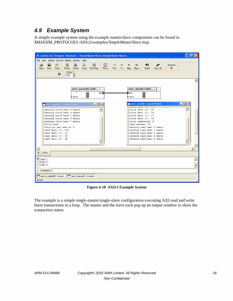
4.9 Example System
A simple example system using the example master/slave components can be found in
$MAXSIM_PROTOCOLS /AXIv2/examples/SimpleMasterSlave.mxp.
Figure 4-10 AXIv2 Example System
The example is a simple single-master/single-slave configuration executing AXI read and write
burst transactions in a loop. The master and the slave each pop up an output window to show the
transaction status.

ARM DUI 0998B Copyright© 2016 ARM Limited. All Rights Reserved 19
Non-Confidential
4.10 Disk Backed Memory Functionality
The AXI4*_Mem component allows systems to model very large memories (several GBs) using
a feature called Disk Backed Memory. This feature helps contain SoC Designer memory usage
within the limits imposed by the operating systems.
Disk Backed Memory achieves this by swapping the contents of the simulated memory to the
disk when the simulated memory exceeds a certain limit. The content swapped to the disk is
usually the oldest content, while the most recent content remains in memory.
As general guidelines, this feature should be enabled if the memory being modeled is larger than
2GB.
Note: Be aware that enabling disk backed memory may affect performance. By default, the
functionality is disabled.
This feature is enabled and controlled using the following parameters:
Disk Backed Memory – This parameter enables/disables Disk Backed Memory
functionality. It is disabled by default.
Disk Backed Memory Size (Bytes) – This parameter should match the size of
addressable space of the memory instance. For example, if an AXI4*_Mem instance
called Mem1 is required to address 0x8000:0000 to 0xFFFF:FFFF (2GB), then this
parameter should be set to 0x80000000 (0xFFFF:FFFF minus 0x8000:0000) for Mem1.
The default is 100 GB.
Disk Backed Memory-RAM Limit (MB) – This parameter determines how much
physical RAM each instance consumes before swapping starts. The default setting of
250 MB should work well for most users; however, if you want to fine-tune these
settings, allocate more RAM to the most frequently-accessed memory instance.
Note: The sum of all RAM Limit settings should not exceed 4GB (this is the current
implementation limit). This does not limit the amount of memory being modeled;
rather, it limits the RAM consumption of SoC Designer.
ARM DUI 0998B Copyright© 2016 ARM Limited. All Rights Reserved 20
Non-Confidential
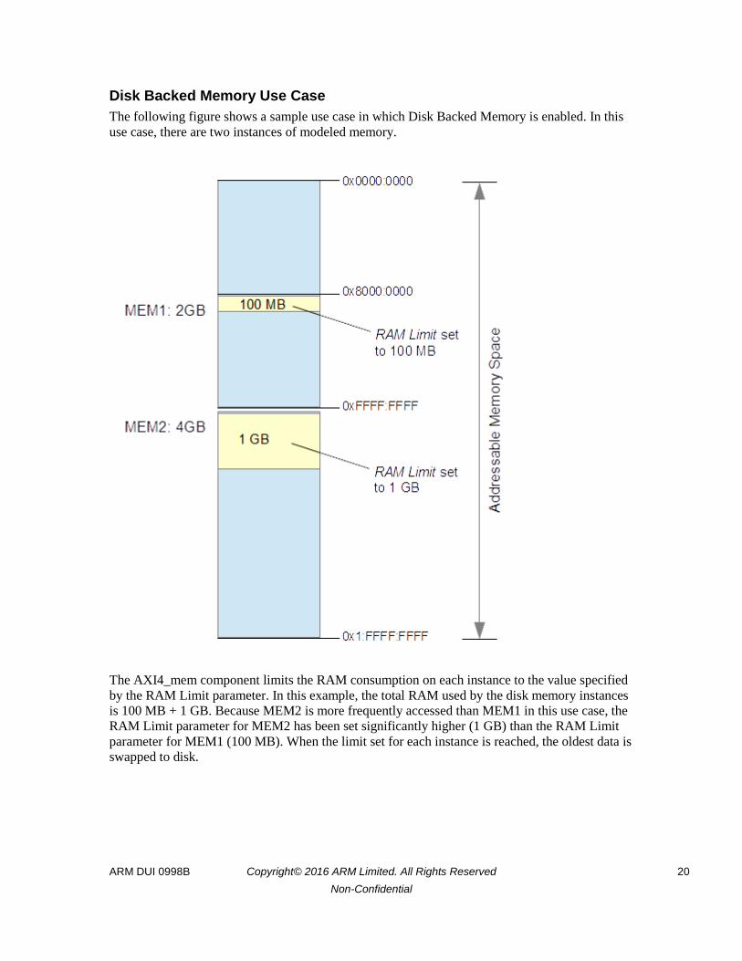
Disk Backed Memory Use Case
The following figure shows a sample use case in which Disk Backed Memory is enabled. In this
use case, there are two instances of modeled memory.
The AXI4_mem component limits the RAM consumption on each instance to the value specified
by the RAM Limit parameter. In this example, the total RAM used by the disk memory instances
is 100 MB + 1 GB. Because MEM2 is more frequently accessed than MEM1 in this use case, the
RAM Limit parameter for MEM2 has been set significantly higher (1 GB) than the RAM Limit
parameter for MEM1 (100 MB). When the limit set for each instance is reached, the oldest data is
swapped to disk.
ARM DUI 0998B Copyright© 2016 ARM Limited. All Rights Reserved 21
Non-Confidential
5 Probes
The following simulation probes are included in the AXIv2 Protocol Bundle.
Name Description
AXIv2 Tracer Enables tracing of AXI signals on an AXIv2 connection. Traced
signals can be viewed in the SoC Designer simulator waveform
window.
AXIv2 BreakPoint Transaction breakpoint on an AXIv2 connection.
AXIv2 Profiler Profiles AXIv2 transactions. Profiled data can be viewed in the
SoC Designer Simulator Profiler window.
AXIv2 Monitor View the activity over the connection for each cycle.
Table 5-1 AXIv2 Probes
ARM DUI 0998B Copyright© 2016 ARM Limited. All Rights Reserved 22
Non-Confidential
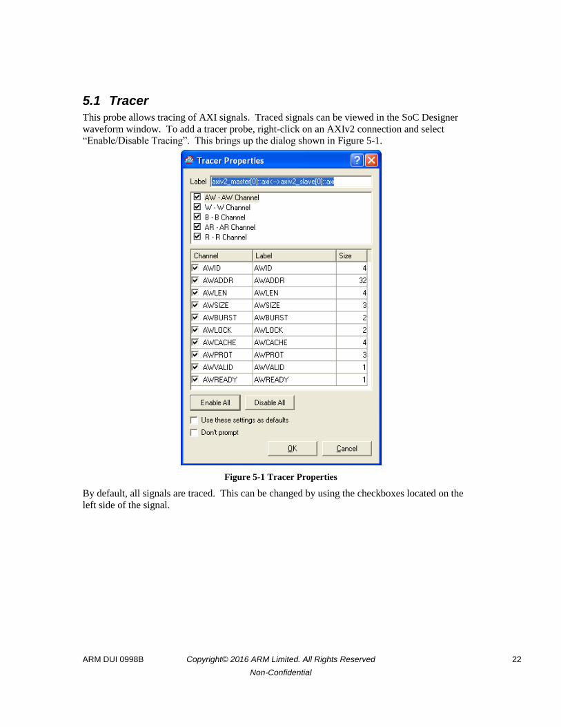
5.1 Tracer
This probe allows tracing of AXI signals. Traced signals can be viewed in the SoC Designer
waveform window. To add a tracer probe, right-click on an AXIv2 connection and select
“Enable/Disable Tracing”. This brings up the dialog shown in Figure 5-1.
Figure 5-1 Tracer Properties
By default, all signals are traced. This can be changed by using the checkboxes located on the
left side of the signal.

ARM DUI 0998B Copyright© 2016 ARM Limited. All Rights Reserved 23
Non-Confidential
5.2 Breakpoint
To insert a breakpoint probe, either double-click on the connection or right-click on the
connection and select “Insert/Remove Breakpoint”. By default, the breakpoint will be activated
and will break on any active AXI transaction across the connection. To configure breakpoint
conditions, bring up the breakpoint property dialog by right-clicking on the connection and
selecting “Edit Breakpoint Properties”.
Figure 5-2 Breakpoint Properties
5.3 Profiling
This probe enables latency profiling over an AXIv2 connection. To enable this probe, right-click
on a connection and select “Profiler”, then “Enable”. Then select the “Display” option to bring
up the Operation vs. Cycles profiling window.

ARM DUI 0998B Copyright© 2016 ARM Limited. All Rights Reserved 24
Non-Confidential
Figure 5-3 Profiling Display
To view other available profiling streams, open the Profiling Manager and locate the connection
to which the profiling probe was attached. There are four separate streams available for profiling
an AXIv2 connection:
Latency: latency for each operation type
Address: plots the accessed address location
Channels Usage: AXI events when channel is active
Channels Transfers: AXI events when a transfer is completed
5.4 Monitor
This probe enables monitoring of an AXIv2 connection for each cycle. To enable this probe,
right-click on a connection and select “Insert/Remove Monitor”.
Figure 5-4 Monitor Display
The default view shows the basic information for each of the 5 AXI channels. The “>>” button
on the top-left can be used to expand the monitor to window to show the transaction details.
5-5 Monitor Details

ARM DUI 0998B Copyright© 2016 ARM Limited. All Rights Reserved 25
Non-Confidential
The combo box on the top can be used to switch to view the open transactions or the history of all
completed transactions. The closed transaction view is shown below.
5-6 Closed Transactions view
5-7 Write to File
From the Channels view, you can dump out the monitor contents to a file by checking the “Write
to file” option as shown above. You can use the “Browse…” button to specify the output file.
6 Component Wizard
The SoC Designer component wizard supports generation of AXIv2 master and slave ports.
Note: Refer to the SoC Designer User Guide for general information regarding the Component
Wizard.
6.1 Generating AXIv2 Ports
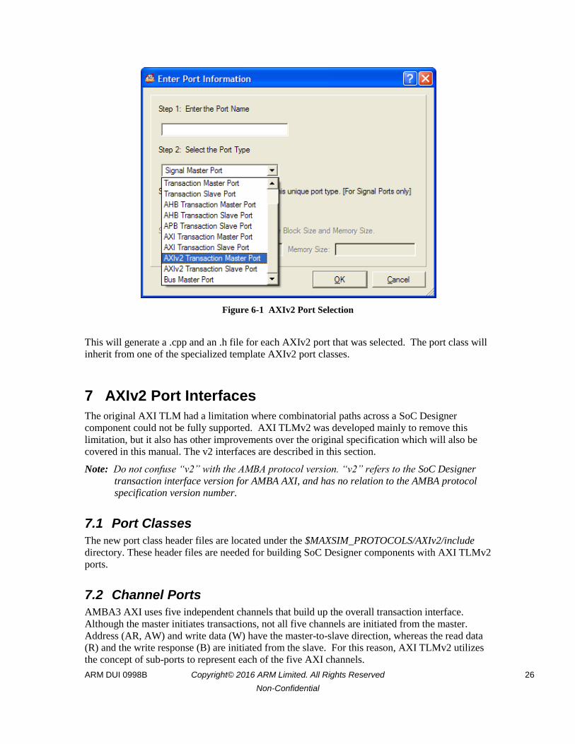
To generate a model with AXIv2 ports, launch the component wizard from SoC Designer Canvas
and proceed to the port definition step. Click on New to create a new port, and select the desired
AXIv2 port type from the port type drop-down list, as shown below:
ARM DUI 0998B Copyright© 2016 ARM Limited. All Rights Reserved 26
Non-Confidential
Figure 6-1 AXIv2 Port Selection
This will generate a .cpp and an .h file for each AXIv2 port that was selected. The port class will
inherit from one of the specialized template AXIv2 port classes.
7 AXIv2 Port Interfaces
The original AXI TLM had a limitation where combinatorial paths across a SoC Designer
component could not be fully supported. AXI TLMv2 was developed mainly to remove this
limitation, but it also has other improvements over the original specification which will also be
covered in this manual. The v2 interfaces are described in this section.
Note: Do not confuse “v2” with the AMBA protocol version. “v2” refers to the SoC Designer
transaction interface version for AMBA AXI, and has no relation to the AMBA protocol
specification version number.
7.1 Port Classes
The new port class header files are located under the $MAXSIM_PROTOCOLS/AXIv2/include
directory. These header files are needed for building SoC Designer components with AXI TLMv2
ports.
7.2 Channel Ports
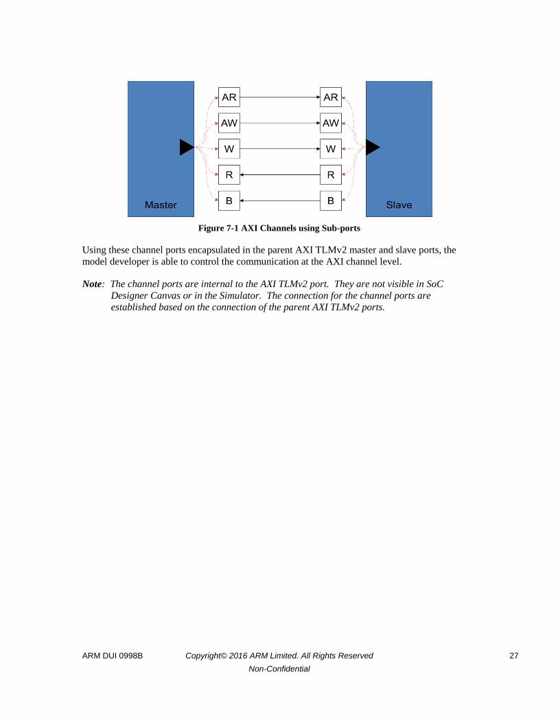
AMBA3 AXI uses five independent channels that build up the overall transaction interface.
Although the master initiates transactions, not all five channels are initiated from the master.
Address (AR, AW) and write data (W) have the master-to-slave direction, whereas the read data
(R) and the write response (B) are initiated from the slave. For this reason, AXI TLMv2 utilizes
the concept of sub-ports to represent each of the five AXI channels.
ARM DUI 0998B Copyright© 2016 ARM Limited. All Rights Reserved 27
Non-Confidential
Figure 7-1 AXI Channels using Sub-ports
Using these channel ports encapsulated in the parent AXI TLMv2 master and slave ports, the
model developer is able to control the communication at the AXI channel level.
Note: The channel ports are internal to the AXI TLMv2 port. They are not visible in SoC
Designer Canvas or in the Simulator. The connection for the channel ports are
established based on the connection of the parent AXI TLMv2 ports.
ARM DUI 0998B Copyright© 2016 ARM Limited. All Rights Reserved 28
Non-Confidential
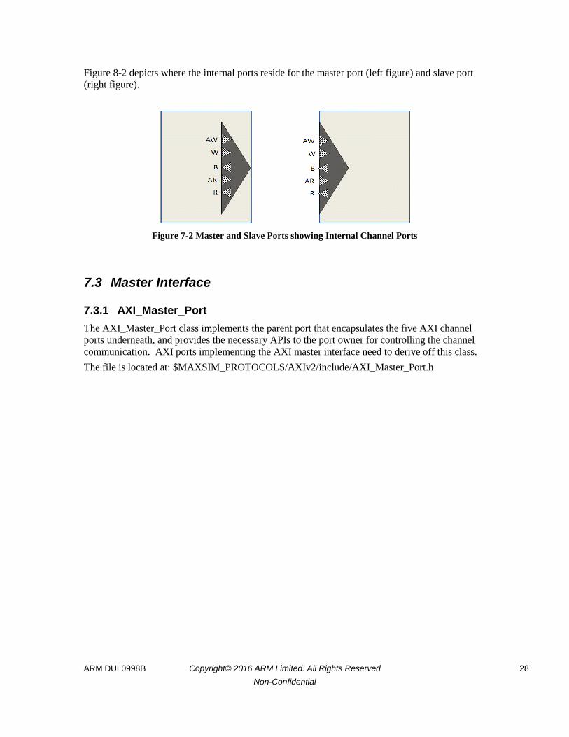
Figure 8-2 depicts where the internal ports reside for the master port (left figure) and slave port
(right figure).
Figure 7-2 Master and Slave Ports showing Internal Channel Ports
7.3 Master Interface
7.3.1 AXI_Master_Port
The AXI_Master_Port class implements the parent port that encapsulates the five AXI channel
ports underneath, and provides the necessary APIs to the port owner for controlling the channel
communication. AXI ports implementing the AXI master interface need to derive off this class.
The file is located at: $MAXSIM_PROTOCOLS/AXIv2/include/AXI_Master_Port.h
ARM DUI 0998B Copyright© 2016 ARM Limited. All Rights Reserved 29
Non-Confidential
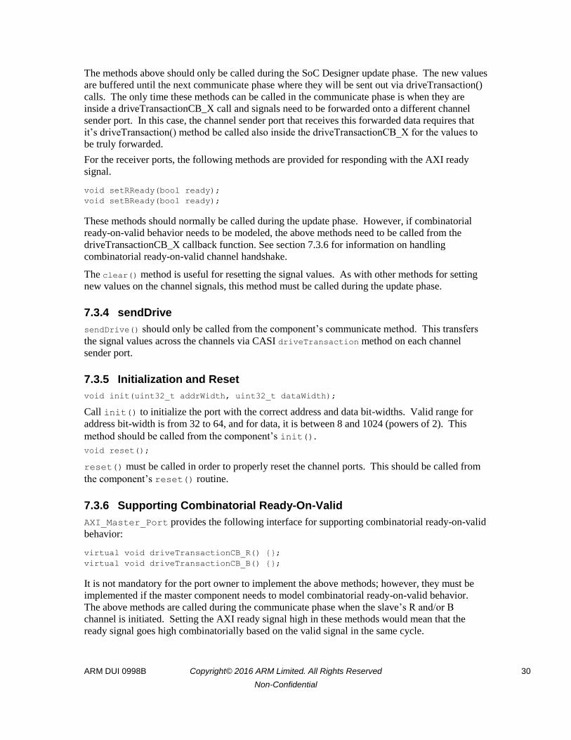
7.3.2 AXI Sender and Receiver Ports for AXI Master Interface
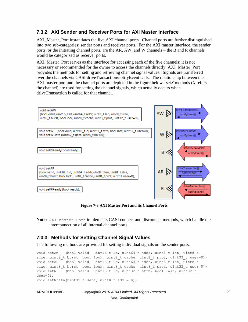
AXI_Master_Port instantiates the five AXI channel ports. Channel ports are further distinguished
into two sub-categories: sender ports and receiver ports. For the AXI master interface, the sender
ports, or the initiating channel ports, are the AR, AW, and W channels – the B and R channels
would be categorized as receiver ports.
AXI_Master_Port serves as the interface for accessing each of the five channels: it is not
necessary or recommended for the owner to access the channels directly. AXI_Master_Port
provides the methods for setting and retrieving channel signal values. Signals are transferred
over the channels via CASI driveTransaction/notifyEvent calls. The relationship between the
AXI master port and the channel ports are depicted in the figure below. setX methods (X refers
the channel) are used for setting the channel signals, which actually occurs when
driveTransaction is called for that channel.
Figure 7-3 AXI Master Port and its Channel Ports
Note: AXI_Master_Port implements CASI connect and disconnect methods, which handle the
interconnection of all internal channel ports.
7.3.3 Methods for Setting Channel Signal Values
The following methods are provided for setting individual signals on the sender ports.
void setAW (bool valid, uint16_t id, uint64_t addr, uint8_t len, uint8_t
size, uint8_t burst, bool lock, uint8_t cache, uint8_t prot, uint32_t user=0);
void setAR (bool valid, uint16_t id, uint64_t addr, uint8_t len, uint8_t
size, uint8_t burst, bool lock, uint8_t cache, uint8_t prot, uint32_t user=0);
void setW (bool valid, uint16_t id, uint32_t strb, bool last, uint32_t
user=0);
void setWData(uint32_t data, uint8_t idx = 0);
ARM DUI 0998B Copyright© 2016 ARM Limited. All Rights Reserved 30
Non-Confidential
The methods above should only be called during the SoC Designer update phase. The new values
are buffered until the next communicate phase where they will be sent out via driveTransaction()
calls. The only time these methods can be called in the communicate phase is when they are
inside a driveTransactionCB_X call and signals need to be forwarded onto a different channel
sender port. In this case, the channel sender port that receives this forwarded data requires that
it’s driveTransaction() method be called also inside the driveTransactionCB_X for the values to
be truly forwarded.
For the receiver ports, the following methods are provided for responding with the AXI ready
signal.
void setRReady(bool ready);
void setBReady(bool ready);
These methods should normally be called during the update phase. However, if combinatorial
ready-on-valid behavior needs to be modeled, the above methods need to be called from the
driveTransactionCB_X callback function. See section 7.3.6 for information on handling
combinatorial ready-on-valid channel handshake.
The clear() method is useful for resetting the signal values. As with other methods for setting
new values on the channel signals, this method must be called during the update phase.
7.3.4 sendDrive
sendDrive() should only be called from the component’s communicate method. This transfers
the signal values across the channels via CASI driveTransaction method on each channel
sender port.
7.3.5 Initialization and Reset
void init(uint32_t addrWidth, uint32_t dataWidth);
Call init() to initialize the port with the correct address and data bit-widths. Valid range for
address bit-width is from 32 to 64, and for data, it is between 8 and 1024 (powers of 2). This
method should be called from the component’s init().
void reset();
reset() must be called in order to properly reset the channel ports. This should be called from
the component’s reset() routine.
7.3.6 Supporting Combinatorial Ready-On-Valid
AXI_Master_Port provides the following interface for supporting combinatorial ready-on-valid
behavior:
virtual void driveTransactionCB_R() {};
virtual void driveTransactionCB_B() {};
It is not mandatory for the port owner to implement the above methods; however, they must be
implemented if the master component needs to model combinatorial ready-on-valid behavior.
The above methods are called during the communicate phase when the slave’s R and/or B
channel is initiated. Setting the AXI ready signal high in these methods would mean that the
ready signal goes high combinatorially based on the valid signal in the same cycle.
ARM DUI 0998B Copyright© 2016 ARM Limited. All Rights Reserved 31
Non-Confidential
7.4 Slave Interface
7.4.1 AXI_Slave_Port
The AXI_Slave_Port class, similar to AXI_Master_Port, implements the parent transaction slave
port that encapsulates the five AXI channel ports underneath, and provides the necessary APIs to
the port owner for controlling the channel communication. AXI ports implementing the AXI
slave interface need to derive off this class.
The file is located at: $MAXSIM_PROTOCOLS/AXIv2/include/AXI_Slave_Port.h
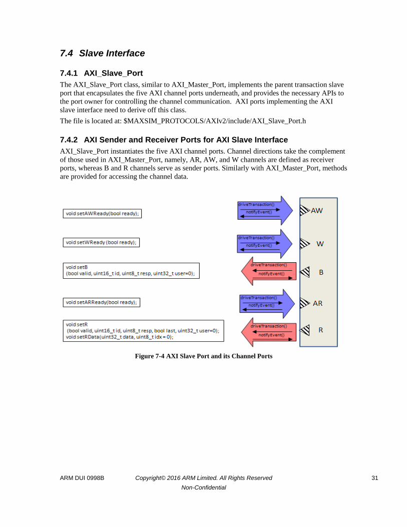
7.4.2 AXI Sender and Receiver Ports for AXI Slave Interface
AXI_Slave_Port instantiates the five AXI channel ports. Channel directions take the complement
of those used in AXI_Master_Port, namely, AR, AW, and W channels are defined as receiver
ports, whereas B and R channels serve as sender ports. Similarly with AXI_Master_Port, methods
are provided for accessing the channel data.
Figure 7-4 AXI Slave Port and its Channel Ports
ARM DUI 0998B Copyright© 2016 ARM Limited. All Rights Reserved 32
Non-Confidential
7.4.3 Methods for Setting Channel Signal Values
The following methods are provided for setting individual signals on the sender ports.
void setR (bool valid, uint16_t id, uint8_t resp, bool last, uint32_t user=0);
void setRData(uint32_t data, uint8_t idx = 0);
void setB (bool valid, uint16_t id, uint8_t resp, uint32_t user=0);
The methods above should only be called during the SoC Designer update phase. The new values
are buffered until the next communicate phase, where they will be sent out via driveTransaction()
calls.
The clear() method is useful for resetting the signal values. As with other methods for setting
new values on the channel signals, this method must be called during the update phase.
For the receiver ports, the following methods are provided for responding with the AXI ready
signal.
void setARReady(bool ready);
void setAWReady(bool ready);
void setWReady(bool ready);
These methods are the same as the AXI_Master_Port’s setXReady methods in terms of their
usage.
7.4.4 sendDrive
sendDrive() should only be called from the component’s communicate method. This transfers the
signal values across the channels via CASI driveTransaction method for each sender channel port.
7.4.5 Initialization and Reset
void init(uint32_t addrWidth, uint32_t dataWidth);
Call init() to initialize the port with the correct address and data bit-widths. Valid range for
address bit-width is from 32 to 64, and for data, it is between 8 and 1024 (powers of 2). This
method should be called from the component’s init().
void reset();
reset() must be called in order to properly reset the channel ports. This should be called from the
component’s reset() routine.
7.5 Note on using large AXI ID widths
AXIv2 master and slave channel access methods have a limit of 16 bits for accessing the AXI ID
field. If your design uses wider ID widths, you can overload the AXIv2 set methods as shown
below.
class MyLargeIDWidthMasterPort : public AXI_Master_Port {
public:
// overloaded setAW method
void setAW(bool valid, uint64_t id, uint64_t addr, uint8_t len, uint8_t
size, uint8_t burst, bool lock, uint8_t cache, uint8_t prot, uint32_t user=0)
{
AXI_Master_Port::setAW(valid, id, addr, len, size, burst, lock, cache,
prot, user);
setSig(AW_ID, id);
}
ARM DUI 0998B Copyright© 2016 ARM Limited. All Rights Reserved 33
Non-Confidential
};
As can be seen from above, AXI_Master_Port::setAW() is used for setting the values for
fields other than the ID, then a setSig() is called for setting the ID value, which can be larger
than 16 bits. An example for overloading the setAW method is shown here; you can take a
similar approach for overloading the set method for other channels.
7.6 Examples
Pseudo-code examples are presented in this section for AXI master and slave using AXI TLMv2
ports.
7.6.1 AXI Master
7.6.1.1 AXI Master Port
Derive the port from AXI_Master_Port class, and inherit driveTransactionCB_X methods for
supporting ready-on-valid.
#include "AXI_Master_Port.h"
class MyAxiMasterPort : public AXI_Master_Port
{
public:
MyAxiMasterPort(CASIModule* owner, std::string name);
virtual void driveTransactionCB_R();
virtual void driveTransactionCB_B();
};
Here is what driveTransactionCB_X method implementation may look like:
void MyAxiMasterPort::driveTransactionCB_R()
{
if (getSig(R_VALID))
this->setRReady(1);
}
void MyAxiMasterPort::driveTransactionCB_B()
{
if (getSig(B_VALID))
this->setBReady(1);
}
Note: driveTransactionCB_X need only be defined if the master port needs to model ready-
on-valid behavior.
7.6.1.2 AXI Master Component
Summarizing the requirements from the previous section:
Driving output values on the channel ports must only occur during the communicate
phase
Setting signal values must only occur during the update phase

ARM DUI 0998B Copyright© 2016 ARM Limited. All Rights Reserved 34
Non-Confidential
Accordingly, the following shows the sequence of events for an AXI master’s communicate and
update methods.
void AXI_Master::communicate()
{
// send out the channel signals from previous update
AXI_TMaster->sendDrive();
}
void AXI_Master::update()
{
AXI_TMaster->clear();
// handle active channel requests and responses
if (AXI_TMaster->getSig(R_VALID) && AXI_TMaster->getSig(R_READY))
{
// process RDATA
My_RDATA = AXI_TMaster->getRData(i);
…
}
if (AXI_TMaster->getSig(B_VALID) && AXI_TMaster->getSig(B_READY))
{
// done with a write transaction
}
if (AXI_TMaster->getSig(AR_VALID) && AXI_TMaster->getSig(AR_READY))
{
…
}
…
// new channel requests
AXI_TMaster->setAR(…);
AXI_TMaster->setAW(…);
}
7.6.2 AXI Slave
7.6.2.1 AXI Slave Port
Derive the port from AXI_Slave_Port class, and inherit driveTransactionCB_X methods for
supporting ready-on-valid.
#include "AXI_Slave_Port.h"
#include "AXI_Receiver_Port.h"
class MyAxiSlavePort : public AXI_Slave_Port
{
public:
MyAxiSlavePort(CASIModule* owner, std::string name);
virtual void driveTransactionCB_AR();
virtual void driveTransactionCB_AW();
virtual void driveTransactionCB_W();
};

ARM DUI 0998B Copyright© 2016 ARM Limited. All Rights Reserved 35
Non-Confidential
Here is what driveTransactionCB_X method implementations may look like:
void MyAxiSlavePort::driveTransactionCB_AR()
{
if (getSig(AR_VALID))
this->setARReady(1);
}
void MyAxiSlavePort::driveTransactionCB_AW()
{
if (getSig(AW_VALID))
this->setAWReady(1);
}
void MyAxiSlavePort::driveTransactionCB_W()
{
if (getSig(W_VALID))
this->setWReady(1);
}
7.6.2.2 AXI Slave Component
Modeling requirements for an AXI slave component are the same as those for an AXI master
component: channel communication, or driving out of channel signal values during communicate,
and sequential logic and setting of new signal values during update.
void AXI_Slave::communicate()
{
AXI_TSlave->sendDrive();
}
void AXI_Slave::update()
{
// clear signals
AXI_TSlave->setR(false, 0, 0, 0);
AXI_TSlave->setB(false, 0, 0);
AXI_TSlave->setAWReady(false);
AXI_TSlave->setARReady(false);
AXI_TSlave->setWReady(false);
// handle active channel requests
if (AXI_TSlave->getSig(AR_VALID) && AXI_TSlave->getSig(AR_READY))
{
…
}
// handle new channel requests
AXI_TSlave->setR(true, it->first, 0, isLastBeat);
}
ARM DUI 0998B Copyright© 2016 ARM Limited. All Rights Reserved 36
Non-Confidential
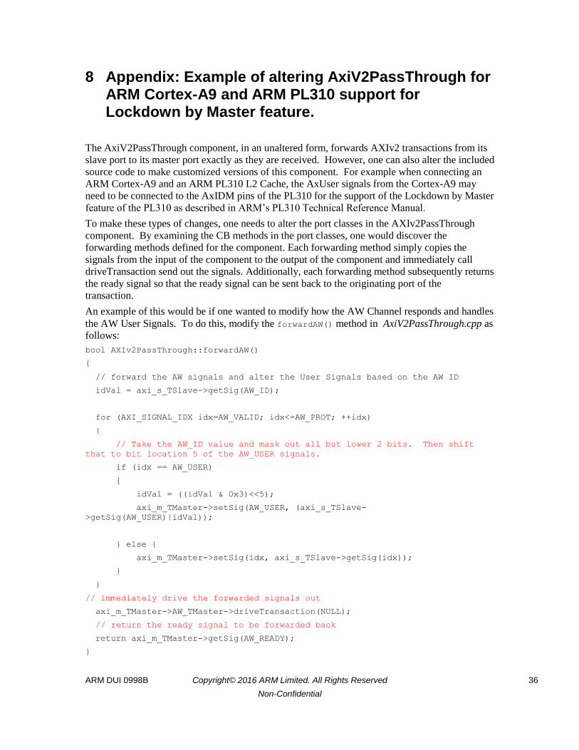
8 Appendix: Example of altering AxiV2PassThrough for ARM Cortex-A9 and ARM PL310 support for Lockdown by Master feature.
The AxiV2PassThrough component, in an unaltered form, forwards AXIv2 transactions from its
slave port to its master port exactly as they are received. However, one can also alter the included
source code to make customized versions of this component. For example when connecting an
ARM Cortex-A9 and an ARM PL310 L2 Cache, the AxUser signals from the Cortex-A9 may
need to be connected to the AxIDM pins of the PL310 for the support of the Lockdown by Master
feature of the PL310 as described in ARM’s PL310 Technical Reference Manual.
To make these types of changes, one needs to alter the port classes in the AXIv2PassThrough
component. By examining the CB methods in the port classes, one would discover the
forwarding methods defined for the component. Each forwarding method simply copies the
signals from the input of the component to the output of the component and immediately call
driveTransaction send out the signals. Additionally, each forwarding method subsequently returns
the ready signal so that the ready signal can be sent back to the originating port of the
transaction.
An example of this would be if one wanted to modify how the AW Channel responds and handles
the AW User Signals. To do this, modify the forwardAW() method in AxiV2PassThrough.cpp as
follows:
bool AXIv2PassThrough::forwardAW()
{
// forward the AW signals and alter the User Signals based on the AW ID
idVal = axi_s_TSlave->getSig(AW_ID);
for (AXI_SIGNAL_IDX idx=AW_VALID; idx<=AW_PROT; ++idx)
{
// Take the AW_ID value and mask out all but lower 2 bits. Then shift
that to bit location 5 of the AW_USER signals.
if (idx == AW_USER)
{
idVal = ((idVal & 0x3)<<5);
axi_m_TMaster->setSig(AW_USER, (axi_s_TSlave-
>getSig(AW_USER)|idVal));
} else {
axi_m_TMaster->setSig(idx, axi_s_TSlave->getSig(idx));
}
}
// immediately drive the forwarded signals out
axi_m_TMaster->AW_TMaster->driveTransaction(NULL);
// return the ready signal to be forwarded back
return axi_m_TMaster->getSig(AW_READY);
}


![Internet-Draft Bundle Protocol Application Framework June 2011 · Internet-Draft Bundle Protocol Application Framework June 2011 1. Problem Statement The Bundle Protocol (BP) [RFC5050]](https://img.pdfslide.net/doc/110x75/60d83ffed9a20207870cb2f5/internet-draft-bundle-protocol-application-framework-june-2011-internet-draft-bundle.jpg)

![AXI Protocol Checker v1 - Xilinx · The AXI Protocol Checker core monitors AXI interfaces. When attached to an interface, it ... See ARM AMBA® AXI Protocol v2.0 [Ref 1]. Performance](https://img.pdfslide.net/doc/110x75/5b158bc17f8b9ac7128d1298/axi-protocol-checker-v1-xilinx-the-axi-protocol-checker-core-monitors-axi.jpg)


![ARM system-architecturesusers.nik.uni-obuda.hu/sima/letoltes/Processor_families_Knowledge_… · Components of the AMBA 2 protocol family (1999) [] The AMBA 2 protocol family (AMBA](https://img.pdfslide.net/doc/110x75/5ea76a1df3eb741af75f6d8f/arm-system-components-of-the-amba-2-protocol-family-1999-the-amba-2-protocol.jpg)