Embed Size (px)
Citation preview

B524/B523Datasheet011

Functionaldescription
TheBSeriesSystem-on-a-Module(SoM)isaLTECat1cellulardevicewithsupportforBLE
(BluetoothLE).ItisbasedontheNordicnRF52840micro-controller.
TheBSeriesisdesignedtobeintegratedintoyourcircuitboarddesign,pluggingintoaM.2NGFF
connectoronyourboard,allowingthemoduletobechangedorupgradedeasily.
QuectelEG91-Emodem
LTEcategory1moduleforEMEAAregion
3GPPE-UTRARelease13
Cat1bandssupported:1,3,7,8,20,28A
2Gand3Gfallback(900,1800,and2100MHz)
SupportforEuropeonly(B523)
SupportforEurope,Australia,andNewZealand(B524)atthistime
NordicSemiconductornRF52840SoC
ARMCortex-M4F32-bitprocessor@64MHz
1MBflash,256KBRAM
Bluetooth5:2Mbps,1Mbps,500Kbps,125Kbps
SupportsDSPinstructions,HWacceleratedFloatingPointUnit(FPU)calculations
ARMTrustZoneCryptoCell-310Cryptographicandsecuritymodule
Upto+8dBmTXpower(downto-20dBmin4dBsteps)
NFC-Atag
On-moduleadditional8MBSPIflash
24mixedsignalGPIO(8xAnalog,4xPWM),UART,I2C,SPI
USB2.0fullspeed(12Mbps)
JTAG(SWD)pins
RGBstatuspinsforLED
ResetandModepinsforbuttons
On-moduleMFF2ParticleSIM
Twoon-moduleU.FLconnectorsforexternalantennas
M.2interface
CEcertified
RoHScompliant(lead-free)
OVERVIEW
FEATURES

Interfaces
VCC
VCCisusedtosupplypowertotheQuectelEG91-Ecellularmodule.Therecommendedinput
voltagerangeonthispinisbetween3.6Vto4.3VDC.Makesurethatthesupplycanhandle
currentsofatleast2A.
Note:ThelimitontheB402(u-bloxLTECatM1)is4.2V,soyoushouldlimitVCCto4.2Vtopreserve
compatibilitywithbothmodules.
3V3
3V3isusedtosupplypowertonRF52840,logicICs,memory,etc.and3.3visrecommended.VCC
inputvoltagerangeisbetween3Vto3.6VDC.Makesurethatthesupplycanhandlecurrentsofat
least150mA.
VBus
VBusisconnectedtotheUSBdetectpinofnRF52840toenablestheUSBinterface.The
recommendedinputvoltagerangeisbetween4.35Vto5.5VDC.
BLOCKDIAGRAM
POWER

TherearetworadiosontheB523module.ABLEradio(nRF52840)andacellularradio(Quectel).
Wehaveprovidedtwou.FLconnectorstopluginthecellularandBLEantenna.Thesearerequired
ifyouwishtousethecellularandBLE.IfyoudonotneedBLE,youdonotneedtoconnecttheBLE
antenna.
Number Label Purpose
1 BT Bluetoothantenna(optional)
2 CELL Quectelcellularmodemantenna
3 ANT_DIV LTEcellularreceivediversityantenna
ThethirdconnectoristheLTEcellularreceivediversityantenna.Asecondcellularantennacanbe
connectedtothisconnectortoimproveperformancewhenthedevicewillbemovingathigh
speeds.ItisonlyusedforLTECat1connectionsandisnotsupportedwhenin2Gor3Gmode.This
antennaisnotnecessaryinmostcasesandisnotincludedinevaluationkits.(TheB402doesnot
havethisconnectorasreceivediversityisnotsupportedinLTECatM1mode.)
CertifiedCellularAntenna
SKU Description
ANTCW2EA ParticleCellularFlexAntenna2G/3G/LTE[x1]
ANTCW2TY ParticleCellularFlexAntenna2G/3G/LTETrayof50[x50]
Type:LTEUltraWideBandFlexAntenna
Frequency/band:698MHz-2690MHz
RoHSCompliant
MechanicalSpecs:
Dimensions:97x21x0.2mm
Mounting:3Madhesivebackedforapplicationonnon-metallicsurfaces
Connectortype:FPC+IPEXconnector
Cablelength:210mm
ANTENNA

Gain:4.71dBi
GeneralAntennaGuidance
Theantennaplacementneedstofollowsomebasicrules,asanyantennaissensitivetoits
environment.Mounttheantennaatleast10mmfrommetalcomponentsorsurfaces,ideally
20mmforbestradiationefficiency,andtrytomaintainaminimumofthreedirectionsfreefrom
obstructionstobeabletooperateeffectively.
Needstuningwithactualproductenclosureandallcomponents.
FortheBLEantenna,itisrecommendedtousea2.4GHzsingle-frequencyantennaandnota
2.4GHz+5GHzantenna,soastoavoidlargegainatthefrequencytwiceof2.4GHzwhichcan
causethesecondharmonicradiationof2.4GHztoexceedstandards.
PeripheralType Qty Input(I)/Output(O)
Digital 24(max) I/O
Analog(ADC) 8(max) I
UART 1 I/O
SPI 2 I/O
I2C 2 I/O
USB 1 I/O
PWM 7(max) O
NFC 1 O
TherearesomeoptionalB523modulespecificI/O:
QuectelUSBandVBUS(formodemfirmwareupgrades)
QuectelRingIndicator(RI)output
Note:AllGPIOsareonlyratedat3.3VDCmax.
TheB523modulehas4padsatthebottomexposingtheSWDinterfaceofthenRF52840.This
interfacecanbeusedtodebugyourcodeorreprogramyourB523bootloader,deviceOS,orthe
userfirmware.Weuse4pogo-pinsconnectingtothesepadsduringproductionforfirmware
flashing.
PERIPHERALSANDGPIO
JTAGANDSWD


Memorymap
Bootloader(48KB,@0xF4000)
UserApplication
256KB@0xB4000(DeviceOS3.1andlater)
128KB@0xD4000(DeviceOS3.0andearlier)
System(656KB,@0x30000)
SoftDevice(192KB)
Reserved(4MB,@0x0040000)
OTA(1500KB,@0x00289000)
Reserved(420KB,@0x00220000)
FAC(128KB,@0x00200000)
LittleFS(2M,@0x00000000)
NRF52840FLASHLAYOUTOVERVIEW
EXTERNALSPIFLASHLAYOUTOVERVIEW(DFUOFFSET:0X80000000)

Pinsandbuttondefinitions
PinsSOM0toSOM9willvaryacrossvariousSoMmodules.Forexample,cellular-specificpinsexists
inthisrange.
AdditionallythereareRESERVED3pins,whosefunctionsvarydependingontheSoM.Forexample,
nRF52MCU-basedmodulesusesomeofthesepinsforadditionalADCandGPIO.Theyareableto
beusedasdescribedontheB523,buttheirfunctionmaybebedifferentonfuturemodules.
Formaximumcross-moduleflexibility,youshouldtrytouseonlythecommonpinswhenpossible.
# Pin Common Function nRF52 Description
1 GND GND POWER Systemground.
2 VCC VCC5 POWERSystempowerin,connecttothe+LiPoorsupplyafixed3.6-4.3vpower.
3 GND GND POWER Systemground.
4 VCC VCC POWERSystempowerin,connecttothe+LiPoorsupplyafixed3.6-4.3vpower.
5 GND GND POWER Systemground.
6 VCC VCC POWERSystempowerin,connecttothe+LiPoorsupplyafixed3.6-4.3vpower.
7 GND GND POWER Systemground.
8 VCC VCC POWERSystempowerin,connecttothe+LiPoorsupplyafixed3.6-4.3vpower.
9 GND GND POWER Systemground.
10 3V3 3V3 POWER Systempowerin,supplyafixed3.0-3.6vpower.
11 USBD+ USBD+ IO Data+pinoftheNRF52840USBport.
PINOUTDIAGRAM
PINDESCRIPTION

12 3V3 3V3 POWER Systempowerin,supplyafixed3.0-3.6vpower.
13 USBD- USBD- IO Data-pinoftheNRF52840USBport.
14 NC RESERVED3 NC Leaveunconnected.
15 GND GND POWER Systemground.
16 VUSB VUSB POWERSystempowerin,USBdetectpinfornRF52840.5VonthispinenablestheUSBinterface.
17 NFC1 SOM33 NFCinput
P0.9 NFCantennaconnection.
18 NC RESERVED3 NC Leaveunconnected.
19 NFC2 SOM43 NFCinput
P0.10 NFCantennaconnection.
20 D1 SCL IO P0.27 I2CSCL,anddigitalonlyGPIO.
21 GND GND POWER Systemground.
22 D0 SDA IO P0.26 I2CSDA,anddigitalonlyGPIO.
23 A0 ADC0 IO P0.3 AnaloginputADC02,anddigitalGPIO.
32 MODE MODE IO P0.25 ConnectedtotheMODEbuttoninput,anddigitalonlyGPIO.
33 A1 ADC1 IO P0.4 AnaloginputADC12,anddigitalGPIO.
34 RESET RESET I Active-lowresetinput.
35 A2 ADC2 IO P0.28 AnaloginputADC22,anddigitalGPIO.
36 D9 TX IO P0.6PrimarilyusedasUARTTX,butcanalsobeusedasadigitalGPIO.
37 A3 ADC3 IO P0.29 AnaloginputADC32,anddigitalGPIO.
38 D10 RX IO P0.08PrimarilyusedasUARTRX,butcanalsobeusedasadigitalGPIO.
39 AGND AGND POWER Systemanalogground.
40 D3 RESERVED3 IO P1.10UARTflowcontrolCTS,SCL1(Wire1),SPI1MOSI,digitalonlyGPIO.
41 A4 RESERVED3 IO P0.30 AnaloginputADC42,anddigitalGPIO.
42 D2 RESERVED3 IO P1.02UARTflowcontrolRTS,SDA1(Wire1),SPI1SCK,digitalonlyGPIO.
43 A5 RESERVED3 IO P0.31 AnaloginputADC52,anddigitalGPIO.
44QuectelUSBD+
SOM0 IO Data+pinoftheR410MUSBport.
45 A6 RESERVED3 IO P0.5 AnaloginputADC62,anddigitalGPIO.
46QuectelUSBD-
SOM1 IO Data-pinoftheR410MUSBport.
47 A7 RESERVED3 IO P0.2 AnaloginputADC72,anddigitalGPIO.
48 D8 CS IO P0.7 SPIinterfaceCS,anddigitalonlyGPIO.
49 AGND AGND POWER Systemanalogground.
50 D11 MISO IO P1.8 SPIinterfaceMISO,anddigitalonlyGPIO.
51 NC RESERVED3 NC Leaveunconnected.
52 D12 MOSI IO P1.9 SPIinterfaceMOSI,anddigitalonlyGPIO.
53 NC RESERVED3 NC Leaveunconnected.
54 D13 SCK IO P0.11 SPIinterfaceSCK,anddigitalonlyGPIO.
55 NC RESERVED3 NC Leaveunconnected.
56 GND GND POWER Systemanalogground.
57 NC RESERVED3 NC Leaveunconnected.

58 NC RESERVED3 NC Leaveunconnected.
59 NC RESERVED3 NC Leaveunconnected.
60 NC RESERVED3 NC Leaveunconnected.
61 RGBR RED IO P0.16 RedpinoftheRGBLED.
62 D22 GPIO0 IO P1.1 GPIO0,digitalonly.
63 RGBG GREEN IO P0.15 GreenpinoftheRGBLED.
64 D23 GPIO1 IO P1.3 GPIO1,digitalonly.
65 RGBB BLUE IO P0.14 BluepinoftheRGBLED.
66 D4 PWM0 IO P0.12 SPI1MISO,DigitalonlyGPIO,andPWM0.
67 SIM_VCC1 SOM53 POWER Leaveunconnected,1.8V/3VSIMSupplyOutputfromR410M.
68 D5 PWM1 IO P0.24 DigitalonlyGPIO,andPWM1.
69 SIM_RST1 SOM63 IO Leaveunconnected,1.8V/3VSIMResetOutputfromR410M.
70 D6 PWM2 IO P1.4 DigitalonlyGPIO,andPWM2.
71 SIM_CLK1 SOM73 IO Leaveunconnected,1.8V/3VSIMClockOutputfromR410M.
72 D7 PWM3 IO P0.13 DigitalonlyGPIO,andPWM3.
73 SIM_DATA1 SOM83 IOLeaveunconnected,1.8V/3VSIMDataI/OofR410mwithinternal4.7kpull-up.
74QuectelVBUS
SOM23 IOUSBdetectpinforR410M.5VonthispinenablestheQuectelUSBinterface.
75 QuectelRI SOM94 IO Ringindicator
1ThesepinsareconnectedtotheinternalMFF2SIMandshouldbeleftopen.
2A0-A7are12-bitAnalog-to-Digital(A/D)inputs(0-4095).
3SoM-specificandReservedpinswillvarydependingonmodule.Theyareabletobeusedonthe
B523,buttheirfunctionmaybebedifferentonfuturemodules.
4RIisavailableontheB523(Quectel)butnotontheB402(u-bloxLTEM1)
5TheVCCmaximumis4.3VontheB523(Quectel)butis4.2VontheB402(u-bloxLTEM1).For
compatibilityacrossmodules,limitthisto4.2V.
Bydefault,theTinkerapplicationfirmwareenablestheuseofthebq24195PMICandMAX17043
fuelgauge.ThisinturnusesI2C(D0andD1)andpinA6(PM_INT).IfyouarenotusingthePMICand
fuelgaugeandwithtousethesepinsforotherpurposes,besuretodisablesystempower
configuration.Thissettingispersistent,soyoumaywanttodisableitwithyourmanufacturing
firmwareonly.
System.setPowerConfiguration(SystemPowerConfiguration());
IfyouareusingEthernetwiththeBSeriesSoM,thefollowingpinsareusedbyEthernet:
DeviceOSPin M.2Pin EthernetPin
MISO 50 SPIMISO
MOSI 52 SPIMOSI
SCK 54 SPISCK
A7 47 nRESET
D22 62 nINTERRUPT

D8 48 nCHIPSELECT
SystemRGBLED
UnliketheBoron,theB523moduledoesnothaveanon-moduleRGBsystemstatusLED.Wehave
provideditsindividualcontrolpinsforyoutoconnectanLEDofyourliking.Thiswillallowgreater
flexibilityintheenddesignofyourproducts.
AdetailedexplanationofdifferentcolorcodesoftheRGBsystemLEDcanbefoundhere.
LEDSTATUS

Technicalspecifications
Supplyvoltages
Parameter Symbol Min Typ Max Unit
Supplyvoltages
SupplyInputVoltage VCC -0.3 +4.7 V
SupplyInputVoltage 3V3 -0.3 +3.9 V
VBUSUSBsupplyvoltage VUSB -0.3 +5.8 V
I/Opinvoltage
VI/O,VDD≤3.6V IO -0.3 VDD+0.3 V
VI/O,VDD>3.6V IO -0.3 +3.9 V
NFCantennapincurrent
INFC1/2 NFC1/NFC2 80 mA
Radio
BTRFinputlevel(52840) 10 dBm
Environmental
Storagetemperature -40 +85 °C
[1]Stressesbeyondthoselistedunderabsolutemaximumratingsmaycausepermanentdamage
tothedevice.Thesearestressratingsonly,andfunctionaloperationofthedeviceattheseorany
otherconditionsbeyondthoseindicatedunderrecommendedoperatingconditionsisnotimplied.
Exposuretoabsolute-maximum-ratedconditionsforextendedperiodsmayaffectdevicereliability.
Parameter Symbol Min Typ Max Unit
Supplyvoltages
SupplyInputVoltage VCC +3.6 +3.8 +4.3 V
SupplyInputVoltage 3V3 +3.0 +3.3 +3.6 V
VBUSUSBsupplyvoltage VUSB +4.35 +5.0 +5.5 V
Environmental
Normaloperatingtemperature1 -20 +25 +753 °C
Extendedoperatingtemperature2 -40 +85 °C
HumidityRangeNoncondensing,relativehumidity 95 %
Notes:
1Normaloperatingtemperaturerange(fullyfunctionalandmeet3GPPspecifications).
2Extendedoperatingtemperaturerange(RFperformancemaybeaffectedoutsidenormal
operatingrange,thoughmoduleisfullyfunctional)
3Themaximumoperatingtemperatureis75°ContheB523(Quectel)butis65°ContheB402(u-
bloxLTEM1).Forcompatibilityacrossmodules,limitthisto65°C.
ABSOLUTEMAXIMUMRATINGS[1]
RECOMMENDEDOPERATINGCONDITIONS

Parameter Symbol Min Typ Peak Unit
OperatingCurrent(uCon,peripheralsandradiodisabled) Iidle 4.47 4.48 4.51 mA
OperatingCurrent(uCon,cellularonbutnotconnected) Icell_idle 17.5 34.2 744 mA
OperatingCurrent(uCon,cellularconnectingtotower) Icell_conn_twr 17.9 72.3 711 mA
OperatingCurrent(uCon,cellularconnectingtocloud) Icell_conn_cloud 23.0 93.6 669 mA
OperatingCurrent(uCon,cellularconnectedbutidle) Icell_cloud_idle 22.9 26.8 149 mA
OperatingCurrent(uCon,cellularconnectedandtransmitting) Icell_cloud_tx 113 139 519 mA
STOPmodesleep,GPIOwake-up Istop_gpio 323 538 916 uA
STOPmodesleep,analogwake-up Istop_analog 272 537 948 uA
STOPmodesleep,RTCwake-up Istop_intrtc 264 537 947 uA
STOPmodesleep,BLEwake-up,advertising Istop_ble_adv 604 2260 uA
STOPmodesleep,BLEwake-up,connected Istop_ble_conn 619 1700 uA
STOPmodesleep,serialwake-up Istop_usart 327 537 912 uA
STOPmodesleep,cellularwake-up Istop_cell 18.7 23.1 140 mA
ULPmodesleep,GPIOwake-up Iulp_gpio 53.6 446 uA
ULPmodesleep,analogwake-up Iulp_analog 55.8 420 uA
ULPmodesleep,RTCwake-up Iulp_intrtc 54.8 444 uA
ULPmodesleep,BLEwake-up,advertising Iulp_ble_adv 139 2430 uA
ULPmodesleep,BLEwake-up,connected Iulp_ble_conn 162 1090 uA
ULPmodesleep,serialwake-up Iulp_usart 317 537 938 uA
ULPmodesleep,cellularwake-up Iulp_cell 18.4 22.8 149 mA
HIBERNATEmodesleep,GPIOwake-up Ihib_gpio 29.7 430 uA
HIBERNATEmodesleep,analogwake-up Ihib_analog 30.8 441 uA
1Themin,andparticularlypeak,valuesmayconsistofveryshorttransients.Thetypical(typ)values
arethebestindicatorofoverallpowerconsumptionovertime.Thepeakvaluesindicatethe
absoluteminimumcapacityofthepowersupplynecessary,notoverallconsumption.
POWERCONSUMPTION

Boronhastworadiomodules.
nRF52840
Bluetooth®5,2.4GHz
95dBmsensitivityin1MbpsBluetooth®lowenergymode
103dBmsensitivityin125kbpsBluetooth®lowenergymode(longrange)
20to+8dBmTXpower,configurablein4dBsteps
4GLTEcellularcharacteristicsforEG91-E
Parameter Value
Protocolstack 3GPPRelease13
RAT LTECat1
LTEFDDBands Band28A(700MHz)
Band20(800MHz)
Band8(900MHz)
Band3(1800MHz)
Band1(2100MHz)
Band7(2600MHz)
WCDMABands Band8(900MHz)
Band1(2100)
GSMBands EGSM900(900MHz)
DCS1800(1800MHz)
Powerclass Class4(33dBm±2dB)forEGSM900
Class1(30dBm±2dB)forDCS1800
ClassE2(27dBm±3dB)forEGSM9008-PSK
ClassE2(26dBm±3dB)forDCS18008-PSK
Class3(24dBm±3dB)forWCDMAbands
Class3(23dBm±2dB)forLTEFDDbands
RADIOSPECIFICATIONS

ThesespecificationsarebasedonthenRF52840datasheet.
Symbol Parameter Min Typ Max Unit
VIH Inputhighvoltage 0.7xVDD VDD V
VIL Inputlowvoltage VSS 0.3xVDD V
VOH,SD Outputhighvoltage,standarddrive,0.5mA,VDD≥1.7 VDD-0.4 VDD V
VOH,HDH Outputhighvoltage,highdrive,5mA,VDD>=2.7V VDD-0.4 VDD V
VOH,HDL Outputhighvoltage,highdrive,3mA,VDD>=1.7V VDD-0.4 VDD V
VOL,SD Outputlowvoltage,standarddrive,0.5mA,VDD≥1.7 VSS VSS+0.4 V
VOL,HDH Outputlowvoltage,highdrive,5mA,VDD>=2.7V VSS VSS+0.4 V
VOL,HDL Outputlowvoltage,highdrive,3mA,VDD>=1.7V VSS VSS+0.4 V
IOL,SD CurrentatVSS+0.4V,outputsetlow,standarddrive,VDD≥1.7 1 2 4 mA
IOL,HDH CurrentatVSS+0.4V,outputsetlow,highdrive,VDD>=2.7V 6 10 15 mA
IOL,HDL CurrentatVSS+0.4V,outputsetlow,highdrive,VDD>=1.7V 3 mA
IOH,SD CurrentatVDD-0.4V,outputsethigh,standarddrive,VDD≥1.7 1 2 4 mA
IOH,HDH CurrentatVDD-0.4V,outputsethigh,highdrive,VDD>=2.7V 6 9 14 mA
IOH,HDL CurrentatVDD-0.4V,outputsethigh,highdrive,VDD>=1.7V 3 mA
tRF,15pF Rise/falltime,standarddrivemode,10-90%,15pFload1 9 ns
tRF,25pF Rise/falltime,standarddrivemode,10-90%,25pFload1 13 ns
tRF,50pF Rise/falltime,standarddrivemode,10-90%,50pFload1 25 ns
tHRF,15pF Rise/Falltime,highdrivemode,10-90%,15pFload1 4 ns
tHRF,25pF Rise/Falltime,highdrivemode,10-90%,25pFload1 5 ns
tHRF,50pF Rise/Falltime,highdrivemode,10-90%,50pFload1 8 ns
RPU Pull-upresistance 11 13 16 kΩ
RPD Pull-downresistance 11 13 16 kΩ
CPAD Padcapacitance 3 pF
CPAD_NFC PadcapacitanceonNFCpads 4 pF
INFC_LEAKLeakagecurrentbetweenNFCpadswhendriventodifferentstates
1 10 μA
Riseandfalltimesbasedonsimulations
GPIOdefaulttostandarddrive(2mA)butcanbereconfiguredtohighdrive(9mA)inDeviceOS
2.0.0andlaterusingthe pinSetDriveStrength() function.
I/OCHARACTERISTICS

Mechanicalspecifications
Parameters Value Unit
Width 30 mm
Height 42 mm
Thickness 5.5 mm
Weight 6.2 grams
Dimensionsareinmillimeters.
DIMENSIONSANDWEIGHT
MECHANICALDRAWING
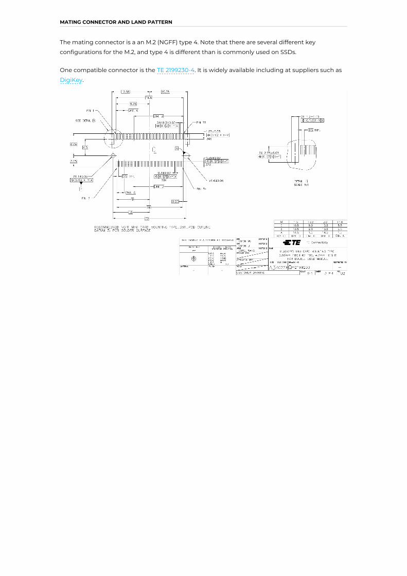
ThematingconnectorisaanM.2(NGFF)type4.Notethatthereareseveraldifferentkey
configurationsfortheM.2,andtype4isdifferentthaniscommonlyusedonSSDs.
OnecompatibleconnectoristheTE2199230-4.Itiswidelyavailableincludingatsupplierssuchas
DigiKey.
MATINGCONNECTORANDLANDPATTERN
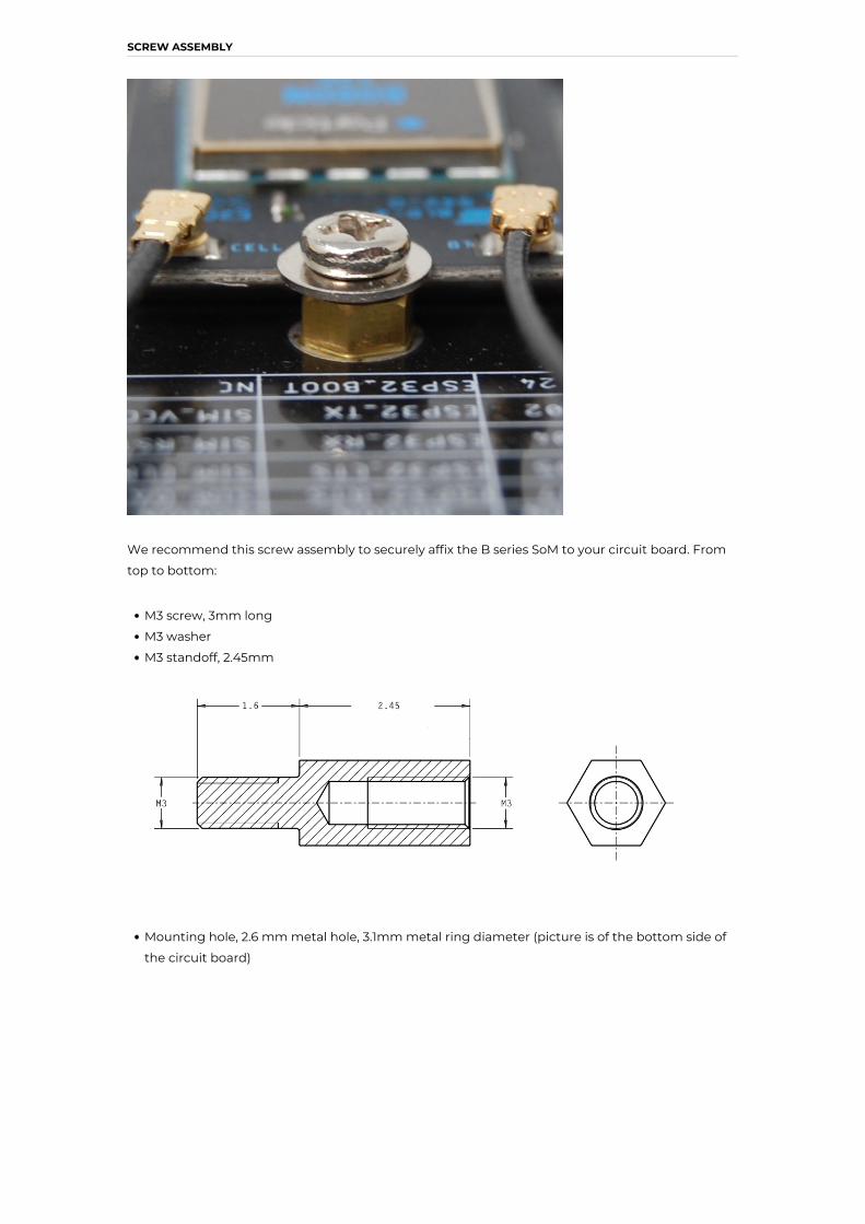
WerecommendthisscrewassemblytosecurelyaffixtheBseriesSoMtoyourcircuitboard.From
toptobottom:
M3screw,3mmlong
M3washer
M3standoff,2.45mm
Mountinghole,2.6mmmetalhole,3.1mmmetalringdiameter(pictureisofthebottomsideof
thecircuitboard)
SCREWASSEMBLY

AnalternativedesignusesaJAESM3ZS067U410-NUT1-R1200standoff.It'sreflowsolderedto
yourbaseboardandhasathreadedholeforaM2*3screwtoholddowntheSoM.Thismaybe
easiertoobtain.
Notethatahold-downscrewisrequiredbecausetheM.2connectordoesnothaveintegrated
locksandtheSoMwillpopupifnotattachedtothebaseboard.
WestronglyrecommendagainstplacingcomponentsundertheSOMboardbecausethereisnot
enoughheight.
DESIGNCONSIDERATIONS


ProductHandling
TheBseriescontainshighlysensitiveelectroniccircuitryandisanElectrostaticSensitiveDevice
(ESD).HandlinganBserieswithoutproperESDprotectionmaydestroyordamageitpermanently.
ProperESDhandlingandpackagingproceduresmustbeappliedthroughouttheprocessing,
handlingandoperationofanyapplicationthatincorporatestheBseriesmodule.ESDprecautions
shouldbeimplementedontheapplicationboardwheretheBseriesismounted.Failureto
observetheseprecautionscanresultinseveredamagetotheBseries!
TheU.FLantennaconnectorisnotdesignedtobeconstantlypluggedandunplugged.The
antennapinisstaticsensitiveandyoucandestroytheradiowithimproperhandling.Atinydabof
glue(epoxy,rubbercement,liquidtapeorhotglue)ontheconnectorcanbeusedsecurelyhold
thepluginplace.
TheM.2edgeconnectorisstaticsensitiveandshouldbehandledcarefully.TheM.2connectoris
notdesignedforrepeatedremovalandinsertionofthemodule.
ESDPRECAUTIONS
CONNECTORS
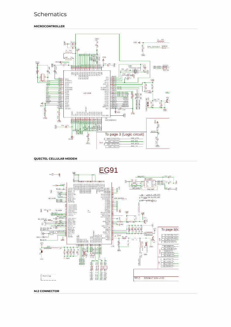
Schematics
MICROCONTROLLER
QUECTELCELLULARMODEM
M.2CONNECTOR

Note:ThelabelsforCTSandRTSarereversedinthisschematic.
SIMANDFLASH
BUFFERS


Defaultsettings
TheBseriescomespre-programmedwithabootloaderandauserapplicationcalledTinker.This
applicationworkswithaniOSandAndroidappalsonamedTinkerthatallowsyoutoveryeasily
toggledigitalpins,takeanaloganddigitalreadingsanddrivevariablePWMoutputs.
Thebootloaderallowsyoutoeasilyupdatetheuserapplicationviaseveraldifferentmethods,USB,
OTA,SerialY-Modem,andalsointernallyviatheFactoryResetprocedure.Allofthesemethods
havemultipletoolsassociatedwiththemaswell.

Countrycompatibility
Country Model Technologies Carriers
Albania B524 2G,3G,Cat1 ALBtelecom,Telekom,Vodafone
Australia B524 3G,Cat1 Optus,Telstra,Vodafone
Austria B524 2G,3G,Cat1 3(Drei),A1,T-Mobile
Belarus B524 2G,3G,Cat1 A1
Belgium B524 2G,3G,Cat1 Base,Orange,Proximus
BosniaandHerzegovina B524 2G,3G BHTelecom,HTEronet
Bulgaria B524 2G,3G A1,Telenor,Vivacom
Croatia B524 2G,3G,Cat1 HrvatskiTelekom,Tele2
Czechia B524 2G,3G,Cat1 O2,T-Mobile,Vodafone
Denmark B524 2G,3G,Cat1 3(Tre),TDC,Telenor,Telia
Estonia B524 2G,3G,Cat1 Elisa,Tele2,Telia
FaroeIslands B524 2G,3G FaroeseTelecom,Vodafone
Finland B524 2G,3G,Cat1 DNA,Elisa,Telia
France B524 2G,3G,Cat1 Bouygues,FreeMobile,Orange,SFR
Germany B524 2G,3G,Cat1 O2,Telekom,Vodafone
Gibraltar B524 2G,3G,Cat1 Gibtel
Greece B524 2G,3G,Cat1 Cosmote,Vodafone,Wind
Hungary B524 2G,3G,Cat1 MagyarTelekom,Telenor,Vodafone
Iceland B524 2G,3G,Cat1 Nova,Siminn,Vodafone
Ireland B524 2G,3G,Cat1 3(Tre),Meteor,O2,Vodafone
Italy B524 2G,3G,Cat1 TIM,Vodafone,Wind
Latvia B524 2G,3G,Cat1 Bite,LMT,Tele2
Liechtenstein B524 2G,3G,Cat1 Mobilkom,Orange
Lithuania B524 2G,3G,Cat1 Bite,Omnitel,Tele2
Luxembourg B524 2G,3G,Cat1 Orange,POST,Tango
Malta B524 2G,3G,Cat1 GoMobile,Vodafone
Moldova B524 2G,3G,Cat1 Moldcell,Orange
Montenegro B524 2G,3G,Cat1 Mtel,T-Mobile,Telenor
Netherlands B524 2G,3G,Cat1 KPN,T-Mobile,Vodafone
NewZealand B524 2G,3G,Cat1 2degrees,Spark,Vodafone
Norway B524 2G,3G,Cat1 TDC,Telenor,Telia
Poland B524 2G,3G,Cat1 Orange,Play,Plus,T-Mobile
Portugal B524 2G,3G,Cat1 NOS,TMN,Vodafone
Romania B524 2G,3G,Cat1 DigiMobil,Orange,TelekomRomania,Vodafone
Serbia B524 2G,3G,Cat1 Telenor,VIP
Slovakia B524 2G,3G,Cat1 O2,Orange,Telekom
Slovenia B524 2G,3G,Cat1 A1,Mobitel
Spain B524 2G,3G,Cat1 Orange,Telefonica,Vodafone,Yoigo
Sweden B524 2G,3G,Cat1 3(Tre),Tele2,Telenor,Telia
Switzerland B524 2G,3G,Cat1 Salt,Sunrise,Swisscom
UnitedKingdom B524 2G,3G,Cat1 3,EE,Manx,O2,Sure,Vodafone

Orderinginformation
SKU Description Region Modem EtherSIM Lifecycle Replacement
B524MEA BSeriesLTECAT-1/3G/2G(Europe)[x1] EMEAA EG91-E ✓ GA
B524MTY BSeriesLTECAT-1/3G/2G(Europe),Tray[x50] EMEAA EG91-E ✓ GA
B523MEA BSeriesLTECAT-1/3G/2G(Europe)[x1] EMEAA EG91-E NRND B524MEA
B523MTY BSeriesLTECAT-1/3G/2G(Europe),Tray[x50] EMEAA EG91-E NRND B524MTY
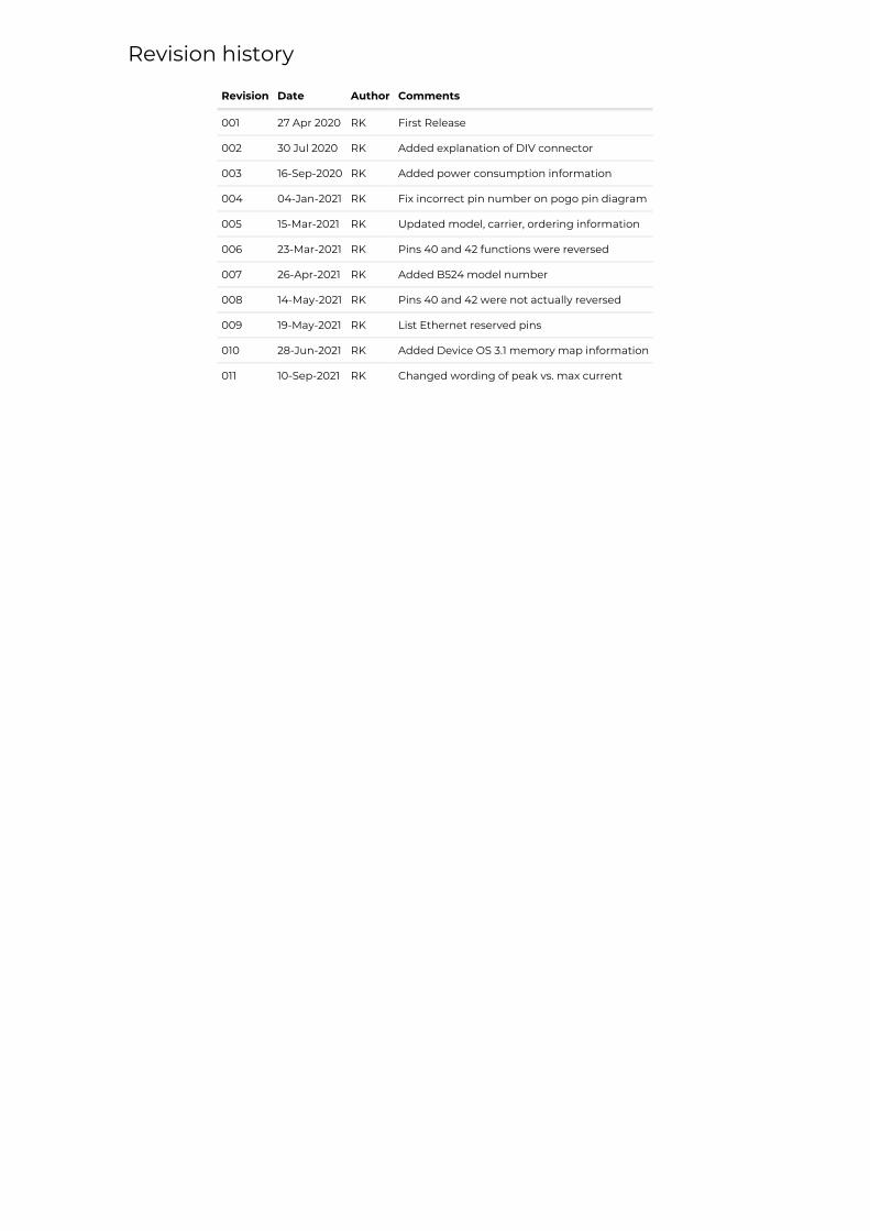
Revisionhistory
Revision Date Author Comments
001 27Apr2020 RK FirstRelease
002 30Jul2020 RK AddedexplanationofDIVconnector
003 16-Sep-2020 RK Addedpowerconsumptioninformation
004 04-Jan-2021 RK Fixincorrectpinnumberonpogopindiagram
005 15-Mar-2021 RK Updatedmodel,carrier,orderinginformation
006 23-Mar-2021 RK Pins40and42functionswerereversed
007 26-Apr-2021 RK AddedB524modelnumber
008 14-May-2021 RK Pins40and42werenotactuallyreversed
009 19-May-2021 RK ListEthernetreservedpins
010 28-Jun-2021 RK AddedDeviceOS3.1memorymapinformation
011 10-Sep-2021 RK Changedwordingofpeakvs.maxcurrent