Embed Size (px)
Citation preview
FP1; Version 1.4
Ballistic Transport in a two-dimensional
Electron System
Ballistischer Transport: Flippern mit Elektronen
Introduction
Gallium arsenide (GaAs) is not only the material of choice for producing high-
frequency electronic semiconductor devices (e.g. the High Electron Mobility Tran-
sistor (HEMT)) used in wireless telecommunications, it also plays an important role
in basic research on semiconductors. In particular, combining GaAs layers with
other materials such as aluminum arsenide (AlAs) or indium arsenide (InAs) opens
a wide playground for the investigation of interesting modern physical phenomena.
Growing a layer sequence GaAs – AlGaAs – AlGaAs:Si1 – AlGaAs with molecu-
lar beam epitaxy one ends up with sheet of electrons accumulated in the GaAs
nearby the GaAs/AlGaAs interface. This is called a two-dimensional electron sys-
tem (2DES). These electrons see only a small disturbing coulomb potential due to
the ionized Si atoms far away from the conducting layer. Consequently they are able
to travel typically some µm without being scattered. Therefore, they are highly sen-
sitive to an external perturbing potential such as periodically etched holes or lines
along their path. An additonally applied external magnetic field perpendicular to
the 2DES forces the electrons on circular orbits with an diameter proportional to 1B
.
Interesting effects occur in the transport properties of such an device if the dia-
meter and the periodicity of the lines or holes are on the same lengthscale. These
phenomena will be studied experimentally in detail here.
In this practical exercise you have the opportunity to learn different aspects of
measuring and handling delicate samples, e.g. the Lock-In technique to detect low
voltages. Furthermore you use superconducting magnets to generate the magnetic
fields required, and methods to cool down samples to 4K and below.
1AlGaAs:Si indicates a doped AlGaAs layer with only a few silicon atoms per thousand.
FP1 Basics
1 Some basic considerations
1.1 2D Electron Systems
One possibility to realize a two-dimensional electron system (2DES) is to epitaxially
grow an AlGaAs-GaAs heterostructure as shown in figure 1a. Electrons originating
from an AlGaAs:Si donor layer move towards the interface between AlGaAs and
GaAs due to the lower conduction band energy in GaAs. As a result positively
charged atoms are left in the donor layer where they set up an electric field in
the space between. This bends the conduction and the valence band such that
a triangular shaped potential well located at the heterointerface is formed in the
conduction band (see Fig. 1b).
PSfrag replacements
GaAs
2DES
Si-doping
AlGaAs
GaAs
Ev
EF
Ec2DES
xy
z
−z
E
a) b)
Figure 1: a) Layer sequence of a GaAs-AlGaAs heterojunction doped with
Si. b) The lower edge of the conduction band Ec and the upper edge of the
valence band Ev as function of the distance of the surface. For clarity, the
layer sequence is repeated below the bandstructure.
While the electron movement within the xy-plane is free, the movement in growth
direction (z-direction) is quantized and the energy of an electron is:
E = Ezi +
(
~2k2
x
2m∗
+~
2k2y
2m∗
)
, (1)
with the quantized subband energy Ezi (i=0, 1, 2, . . .) in z-direction and the effective2
electron mass m∗. With sufficiently low temperature and electron density ns only
the lowest of the energy levels Ez0 is occupied3, so we call our electron system a
two-dimensional electron system (2DES).
2The effective mass represents the influence of the periodic crystal potential.3This is the case for the used AlGaAs/GaAs heterostructures at 4.2K.
2
Basics FP1
The density of states D(E) for such a system is constant within a subband. For the
lowest subband Ez0 is:
D(E) =m∗
π~2. (2)
So for the Fermi energy EF , the Fermi velocity vF and the Fermi wavevector kF
holds:
kF =√
2πns , (3a)
vF =~√
2πns
m∗
, (3b)
EF =~
2πns
m∗
. (3c)
I Exercise 1: Verify the relations given above in equations 3a–3c. ( Start with
calculating the density of states in k-space. Then calculate the area of the Fermi
circle and combine both results to obtain ns for k=kF .)
The simplest way to describe charge transport through such a system is related to
the Drude model. Electrons are accelerated in an external electric field until they
are stopped after a time τ due to scattering (τ does not depend on the magnetic
field). Thus they have the drift velocity ~vD according to:
~vD =eτ
m∗
~E = µ~E , (4)
with µ = eτm∗
called mobility. Carrying charges, the current density is
~ = ens~vD . (5)
Here another quantity describing the electronic system should be introduced, the
mean free path `. Between two scattering events, the electron moves with the Fermi
velocity vF , thus:
` = τvF =~
eµ√
2πns . (6)
The current density ~ and the driving electric field ~E are connected by the conduc-
tivity tensor σ resp. the resistivity tensor ρ as follows (remember that we have a
2D system!):(
jx
jy
)
=
(
σxx σxy
σyx σyy
)
·
(
Ex
Ey
)
, (7a)
(
Ex
Ey
)
=
(
ρxx ρxy
ρyx ρyy
)
·
(
jx
jy
)
. (7b)
3
FP1 Basics
In isotropic systems — and the systems we use are isotropic — the components
of the resistivity tensor are symmetric: ρxx = ρyy and ρxy = −ρyx and it holds
σ = ρ−1.
1.2 Hall Resistivity and longitudinal Resistivity
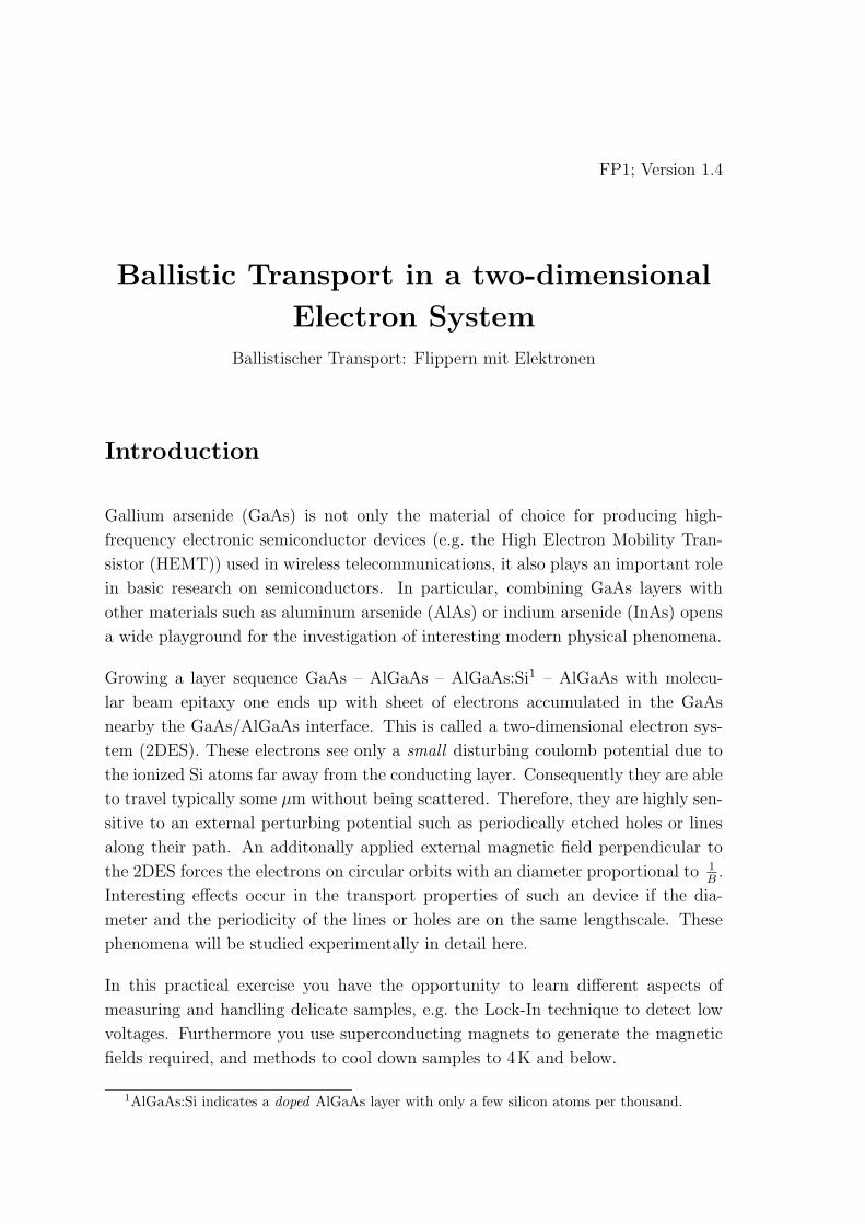
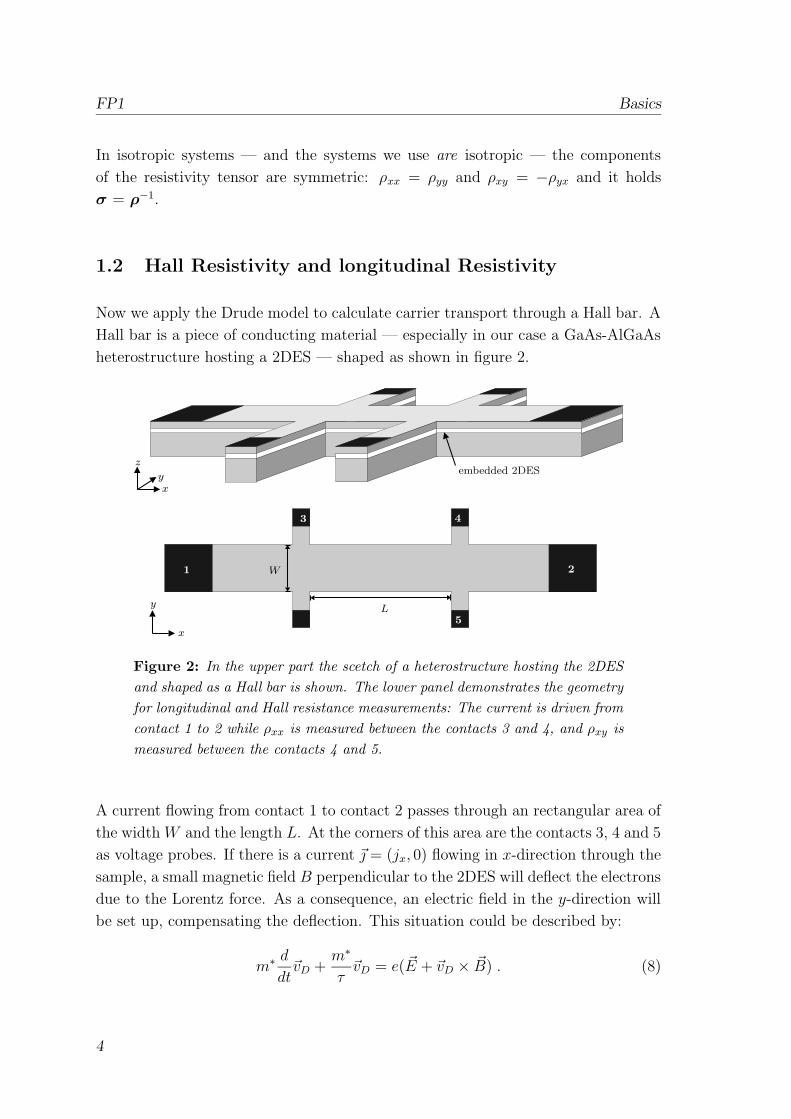
Now we apply the Drude model to calculate carrier transport through a Hall bar. A
Hall bar is a piece of conducting material — especially in our case a GaAs-AlGaAs
heterostructure hosting a 2DES — shaped as shown in figure 2.
PSfrag replacements
1
3 4
2
5
embedded 2DES
L
W
x
x
y
y
z
Figure 2: In the upper part the scetch of a heterostructure hosting the 2DES
and shaped as a Hall bar is shown. The lower panel demonstrates the geometry
for longitudinal and Hall resistance measurements: The current is driven from
contact 1 to 2 while ρxx is measured between the contacts 3 and 4, and ρxy is
measured between the contacts 4 and 5.
A current flowing from contact 1 to contact 2 passes through an rectangular area of
the width W and the length L. At the corners of this area are the contacts 3, 4 and 5
as voltage probes. If there is a current ~ = (jx, 0) flowing in x-direction through the
sample, a small magnetic field B perpendicular to the 2DES will deflect the electrons
due to the Lorentz force. As a consequence, an electric field in the y-direction will
be set up, compensating the deflection. This situation could be described by:
m∗d
dt~vD +
m∗
τ~vD = e( ~E + ~vD × ~B) . (8)
4
Basics FP1
I Exercise 2: Since we measure currents and voltages we need expressions for
the Hall voltage Uxy (U45 in the geometry given in figure 2) and the longitudinal
voltage Uxx (U34 according to figure 2) as a function of the applied magnetic field B.
( Start from equation 8 and assume the stationary case ddt
~vD = 0. Remember that
we are in a two dimensional system, remember that the macroscopic current I flows
only in x-direction, and remember further that the magnetic field ~B is perpendicular
to the 2DES. Set up an equation ~E = r · ~ and compare the components of the
tensor r with the components of the resistivity tensor ρ in equation 7b.) Discuss
the results and explain how the density ns and the mobility µ can be extracted from
measurements of Uxy vs. B and Uxx vs. B.
Since the electrons move on cyclotron orbits, the cyclotron radius Rc and the cy-
clotron frequency ωc are also of interest:
ωc =eB
m∗
, (9a)
Rc =vF
ωc
=~√
2πns
eB. (9b)
The Drude model is only valid for small magnetic fields. At higher magnetic fields
the classical model will break down and we have to use quantum mechanics to
describe our 2DES properly. A hand-waving argument whether we can calculate
classically or not is the following: Assume, that there will be no transport due to
drifting charge carriers if an electron can turn a lot of cyclotron orbits before it is
scattered. Thus, we have to compare the mean free path ` with the cyclotron orbit.
I Exercise 3: Check, up to which magnetic field you can use the drude model
to describe transport through a sample with µ = 1 × 106 cm2/Vs.
To describe the system more accurately in the case we apply higher magnetic fields,
we start with the Schrodinger equation:(
Ei +1
2m∗
(i~∇ + e ~A)2 + U(y)
)
Ψ(x, y) = EΨ(x, y) . (10)
Ei is the subband energy (quantized in z-direction) and ~A is the magnetic vector
potential. The potential U(y) accounts for the geometric restriction due to the Hall
bar. Assuming at a first glance U(y) = 0 inside the Hall bar we achieve the energies:
En = Ei + (n +1
2)~ωc with n = 0, 1, 2, . . . (11)
5
FP1 Basics
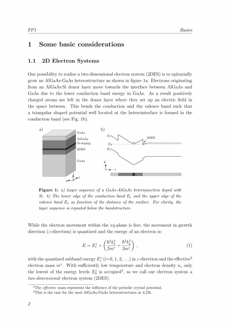
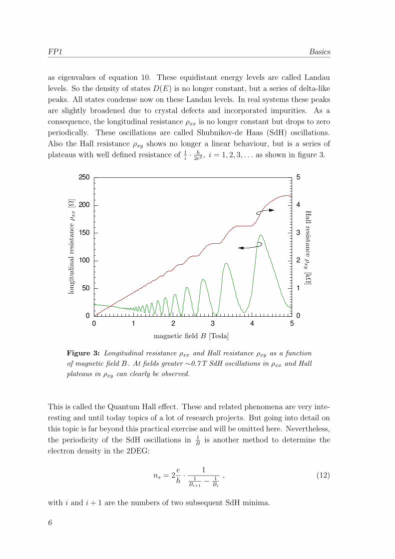
as eigenvalues of equation 10. These equidistant energy levels are called Landau
levels. So the density of states D(E) is no longer constant, but a series of delta-like
peaks. All states condense now on these Landau levels. In real systems these peaks
are slightly broadened due to crystal defects and incorporated impurities. As a
consequence, the longitudinal resistance ρxx is no longer constant but drops to zero
periodically. These oscillations are called Shubnikov-de Haas (SdH) oscillations.
Also the Hall resistance ρxy shows no longer a linear behaviour, but is a series of
plateaus with well defined resistance of 1i· h
2e2 , i = 1, 2, 3, . . . as shown in figure 3.
0 1 2 3 4 50
50
100
150
200
250
0
1
2
3
4
5
PSfrag replacements
longi
tudin
alre
sist
ance
ρxx
[Ω]
magnetic field B [Tesla]
Hall
resistance
ρxy
[kΩ
]
Figure 3: Longitudinal resistance ρxx and Hall resistance ρxy as a function
of magnetic field B. At fields greater ∼0.7T SdH oscillations in ρxx and Hall
plateaus in ρxy can clearly be observed.
This is called the Quantum Hall effect. These and related phenomena are very inte-
resting and until today topics of a lot of research projects. But going into detail on
this topic is far beyond this practical exercise and will be omitted here. Nevertheless,
the periodicity of the SdH oscillations in 1B
is another method to determine the
electron density in the 2DEG:
ns = 2e
h· 1
1Bi+1
− 1Bi
, (12)
with i and i + 1 are the numbers of two subsequent SdH minima.
6
Basics FP1
1.3 Transport through a structured Hall bar
After this short excursion in the Quantum Hall regime, we come back to our clas-
sical ideas of magnetotransport. We can ask ourselves now what happens if we
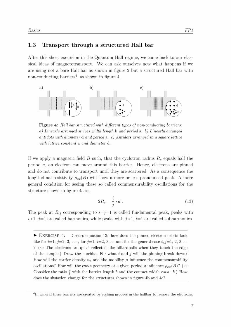
are using not a bare Hall bar as shown in figure 2 but a structured Hall bar with
non-conducting barriers4, as shown in figure 4.PSfrag replacements
a) b) c)
aa
ab dd
Figure 4: Hall bar structured with different types of non-conducting barriers:
a) Linearly arranged stripes width length b and period a. b) Linearly arranged
antidots with diameter d and period a. c) Antidots arranged in a square lattice
with lattice constant a and diameter d.
If we apply a magnetic field B such, that the cyclotron radius Rc equals half the
period a, an electron can move around this barrier. Hence, electrons are pinned
and do not contribute to transport until they are scattered. As a consequence the
longitudinal resistivity ρxx(B) will show a more or less pronounced peak. A more
general condition for seeing these so called commensurability oscillations for the
structure shown in figure 4a is:
2Rc =i
j· a . (13)
The peak at Bij corresponding to i=j=1 is called fundamental peak, peaks with
i>1, j=1 are called harmonics, while peaks with j>1, i=1 are called subharmonics.
I Exercise 4: Discuss equation 13: how does the pinned electron orbits look
like for i=1, j=2, 3, . . . , for j=1, i=2, 3,. . . and for the general case i, j=1, 2, 3,. . .
? ( The electrons are quasi reflected like billardballs when they touch the edge
of the sample.) Draw these orbits. For what i and j will the pinning break down?
How will the carrier density ns and the mobility µ influence the commensurability
oscillations? How will the exact geometry at a given period a influence ρxx(B)? (
Consider the ratio cb
with the barrier length b and the contact width c=a−b.) How
does the situation change for the structures shown in figure 4b and 4c?
4In general these barriers are created by etching grooves in the hallbar to remove the electrons.
7
FP1 Basics
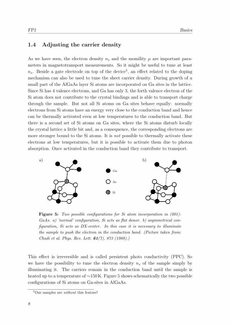
1.4 Adjusting the carrier density
As we have seen, the electron density ns and the momility µ are important para-
meters in magnetotransport measurements. So it might be useful to tune at least
ns. Beside a gate electrode on top of the device5, an effect related to the doping
mechanism can also be used to tune the sheet carrier density. During growth of a
small part of the AlGaAs layer Si atoms are incorporated on Ga sites in the lattice.
Since Si has 4 valence electrons, and Ga has only 3, the forth valence electron of the
Si atom does not contribute to the crystal bindings and is able to transport charge
through the sample. But not all Si atoms on Ga sites behave equally: normally
electrons from Si atoms have an energy very close to the conduction band and hence
can be thermally activated even at low temperatures to the conduction band. But
there is a second set of Si atoms on Ga sites, where the Si atoms disturb locally
the crystal lattice a little bit and, as a consequence, the corresponding electrons are
more stronger bound to the Si atoms. It is not possible to thermally activate these
electrons at low temperatures, but it is possible to activate them due to photon
absorption. Once activated in the conduction band they contribute to transport.
PSfrag replacements
a) b)
Ga
As
Si
Figure 5: Two possible configurations for Si atom incorporation in (001)-
GaAs. a) ’normal’ configuration, Si acts as flat donor. b) asymmetrical con-
figuration, Si acts as DX-center. In this case it is necessary to illuminate
the sample to push the electron in the conduction band. (Picture taken from:
Chadi et al. Phys. Rev. Lett. 61(7), 873 (1988).)
This effect is irreversible and is called persistent photo conductivity (PPC). So
we have the possibility to tune the electron density ns of the sample simply by
illuminating it. The carriers remain in the conduction band until the sample is
heated up to a temperature of ∼150K. Figure 5 shows schematically the two possible
configurations of Si atoms on Ga-sites in AlGaAs.
5Our samples are without this feature!
8
Measurements FP1
2 What we measure and how we do it
2.1 Ingredients
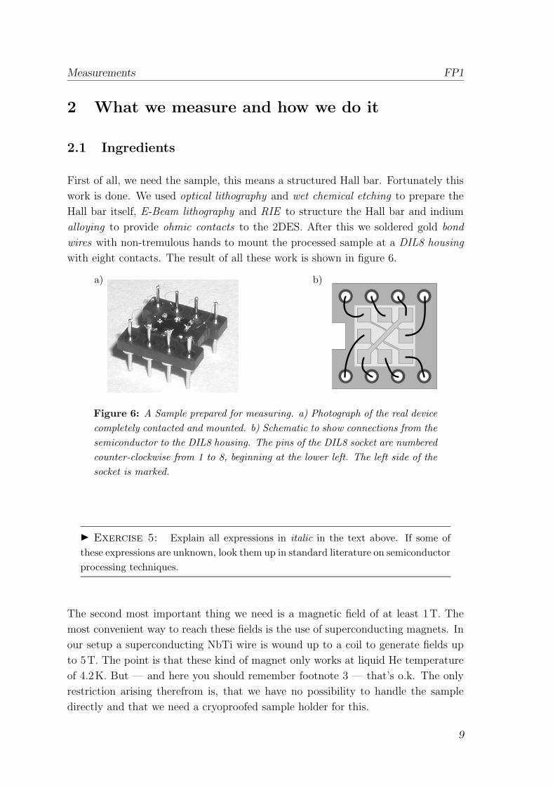
First of all, we need the sample, this means a structured Hall bar. Fortunately this
work is done. We used optical lithography and wet chemical etching to prepare the
Hall bar itself, E-Beam lithography and RIE to structure the Hall bar and indium
alloying to provide ohmic contacts to the 2DES. After this we soldered gold bond
wires with non-tremulous hands to mount the processed sample at a DIL8 housing
with eight contacts. The result of all these work is shown in figure 6.
PSfrag replacements
a) b)
Figure 6: A Sample prepared for measuring. a) Photograph of the real device
completely contacted and mounted. b) Schematic to show connections from the
semiconductor to the DIL8 housing. The pins of the DIL8 socket are numbered
counter-clockwise from 1 to 8, beginning at the lower left. The left side of the
socket is marked.
I Exercise 5: Explain all expressions in italic in the text above. If some of
these expressions are unknown, look them up in standard literature on semiconductor
processing techniques.
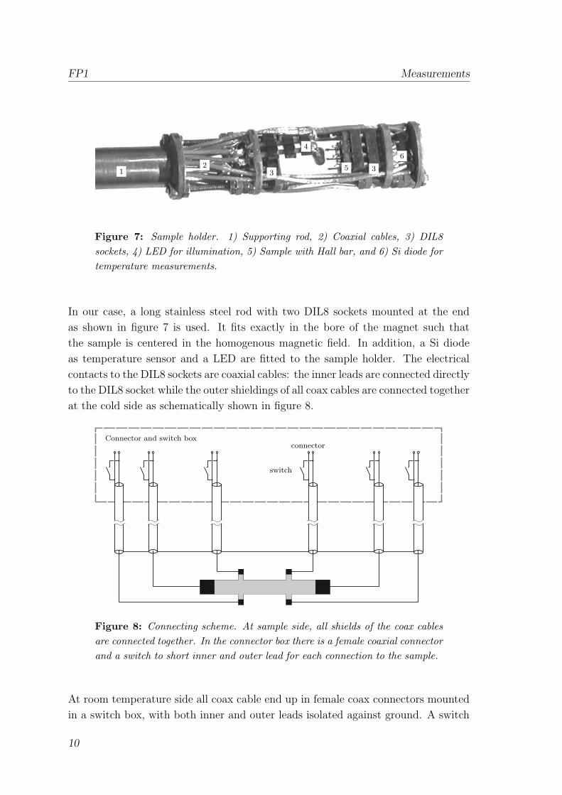
The second most important thing we need is a magnetic field of at least 1T. The
most convenient way to reach these fields is the use of superconducting magnets. In
our setup a superconducting NbTi wire is wound up to a coil to generate fields up
to 5T. The point is that these kind of magnet only works at liquid He temperature
of 4.2K. But — and here you should remember footnote 3 — that’s o.k. The only
restriction arising therefrom is, that we have no possibility to handle the sample
directly and that we need a cryoproofed sample holder for this.
9
FP1 Measurements
PSfrag replacements
12
33
4
5
6
Figure 7: Sample holder. 1) Supporting rod, 2) Coaxial cables, 3) DIL8
sockets, 4) LED for illumination, 5) Sample with Hall bar, and 6) Si diode for
temperature measurements.
In our case, a long stainless steel rod with two DIL8 sockets mounted at the end
as shown in figure 7 is used. It fits exactly in the bore of the magnet such that
the sample is centered in the homogenous magnetic field. In addition, a Si diode
as temperature sensor and a LED are fitted to the sample holder. The electrical
contacts to the DIL8 sockets are coaxial cables: the inner leads are connected directly
to the DIL8 socket while the outer shieldings of all coax cables are connected together
at the cold side as schematically shown in figure 8.
PSfrag replacements
Connector and switch box
switch
connector
Figure 8: Connecting scheme. At sample side, all shields of the coax cables
are connected together. In the connector box there is a female coaxial connector
and a switch to short inner and outer lead for each connection to the sample.
At room temperature side all coax cable end up in female coax connectors mounted
in a switch box, with both inner and outer leads isolated against ground. A switch
10
Measurements FP1
determines whether a particular coax connector at the front is active or not, another
switch short circuits the inner and outer lead. Since we drive only small currents
through the sample (typically 200nA in our case), we expect only small voltages
to measure. A standard technique to do this is to use a ’Lock-In amplifier’ (short:
Lock-In). This is a very sensitive instrument, which amplifies only signals with a
certain choosable frequency f0 and ignores all other signals.
I Exercise 6: Calculate the expected longitudinal voltage Vxx in a 150µm
wide Hall bar with a distance between the voltage probing contacts of 750µm for
B = 0T and a current I = 200nA. Assume that the used 2DES has a sheet carrier
concentration of ns = 2.0× 1011 cm−2 and a mobility of µ = 1.0× 106 cm2/Vs. Why
are we using an Lock-In instead of a ’simple’ Micro-Voltmeter? How does a Lock-In
work in principle? Since nearly every Lock-In has an built-in oscillator to generate
the reference signal needed, can we use the Lock-In not only for measuring but also
as current source? How must the sample be connected? ( The Lock-In provides
the oscillator signal as a voltage adjustable in frequency and amplitude (0V to 2V!)
between the outer and inner lead of a coaxial connector. A Lock-In is also able to
measure two voltages between inner and outer leads of two coax connectors and to
calculate the difference between these two voltages.)
2.2 Behavior in the lab
Before you start your measurements you should keep in mind a few important things
which make your life easier and safer (and certainly also your tutor’s life):
• Working in a lab means having a maximum of discipline. This includes not to
eat or drink, not to smoke, and to keep your fingers away from equipment of
other people’s setups.
• Do not use any equipment unless you are allowed to do so and unless you have
been shown how to use it.
• Be extremely careful handling cryogenic liquids, especially He. The most
known dangers hereby are frozen skin or limbs, damaged equipment and severe
injuries due to exploding vessels, and the risk of suffocation.
• Keep also in mind, that the energy stored in a superconducting coil magnetized
to 1T is enormous. Hence be aware of the breakdown of the superconductivity
(quench) since in this case a lot of liquid He will be evaporated at once!
11
FP1 Measurements
2.3 Tasks to do
Now we have enough background knowledge about a 2DES, a Hall bar and the
theory of magnetotransport experiments, as well as we have some basic technical
informations about the used equipment. So let us begin with the measurements.
1. Explain in detail the equipment in the lab (e.g. x-y-recorder, LockIn, cryostat,
power supply, He handling system and dewar, . . .) and the actions to take in
the case of emergency.
2. Put one of the mounted samples with a bare Hall bar in the sample holder
(do not forget the LED!) and cool down the magnet and the sample to 4.2K
(Since this is a very critical process, do it only together with your tutor).
3. When the magnet and the sample are cold, measure ns and µ of the unillu-
minated sample. Do this by taking ρxx and ρxy as a function of B. Please
pay attention: Not all samples we use have the connection scheme shown in
figure 6b! In doubt, ask your tutor! Do not use higher fields as 3T and drive a
current of max. 200nA through the sample. Choose the appropriate settings
of the Lock-In (gain, time constant, resolution, etc.)! What can you observe?
4. Repeat the measurement after illuminating the sample (60sec, 1mA current
through LED). What has changed now?
5. Use the sample with the linearly arranged stripes (see Fig. 4a) and repeat the
measurement. Assign the observed features to the fundamental, harmonics or
subharmonics and calculate therefrom the period a and the length b and c.
6. If you have to take out the sample holder please ask your tutor to assist you.
Do not handle the system alone, until your tutor told you to do so!
7. Perform the same measurements at the samples with the linearly arranged
dots and the dot arrays. Does the ρxx traces change the way you expected? If
not, why not?
8. After finishing all measurements you planned to do, pull out the magnet (to-
gether with your tutor, for sure), switch off the power supply and put the
sample back in the appropriate case.
9. Collect all your personal things (do not forget your empty bottle of coke!) and
check if you have all the data necessary for discussing your results.
12
Literature FP1
2.4 Discussion of the results
Discuss your results critically. Do you really observe what you expected? Are the
peaks at the correct position according to the given device geometry? If not, what
might be the reason therefore? How many peaks can you resolve? What should be
changed to achieve higher resolution? What might be the limiting factor? What
can you deduce from the linewidth of the peaks? What determines the height of the
resistance maxima?
Literature
The following list is surely not complete and is given here only for your convenience.
Feel free to search for more literature, if you are interested in more details. . .
J. H. Davies: The physics of low-dimensional semiconductors: An introduction,
Cambridge University Press, Cambridge (1998).
S. Datta: Electronic transport in mesoscopic systems, Cambridge University Press,
Cambridge (1995).
M. J. Kelly: Low-Dimensional Semiconductors: Materials, Physics, Technology,
Devices, Clarendon, Oxford (1995).
C. W. J. Beenakker, H. van Houten: Quantum Transport in Semiconductor
Nanostructures, in H. Ehrenreich, D. Turnbull (Hrsg.): Solid State Physics: Ad-
vanced in Research and Application, 44, 1-228 Academic Press (1991).
D. Weiss, M. L. Roukes, A. Menschig, P. Grambow, K. von Klitzing,
G. Weimann: Electron Pinball and Commensurate Orbits in a Periodic Array of
Scatterers, Phys. Rev. Lett. 66(21), 2790-2793 (1991).
D. Weiss, K. Richter: Antidot-Ubergitter: Flippern mit Elektronen, Phys. Bl.
51(3), 171-176 (1995).
T. Ando, Y. Arakawa, K. Furuya, S. Komiyama, H. Nakashima (Eds.):
Mesoscopic Physics and Elektronics, Springer, Berlin, Heidelberg, New York (1998).
W. Menz, P. Bley: Mikrosystemtechnik fur Ingenieure, VCH, Weinheim, New
York, Basel, Cambridge (1993).
H. Beneking: Halbleiter-Technologie, Teubner, Stuttgart (1991).
D. Widmann, H. Mader, H. Friedrich: Technologie hochintegrierter Schaltun-
gen, Springer, Berlin, Heidelberg, New York (1988).
13
FP1 Diagrams
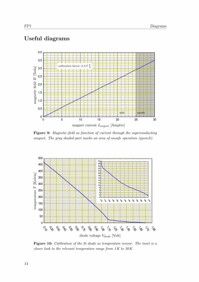
Useful diagrams
0 5 10 15 20 25 300
0,5
1,0
1,5
2,0
2,5
3,0
3,5
4,0
PSfrag replacements
magnet current Imagnet [Ampere]
mag
net
icfiel
dB
[Tes
la] calibration factor: 0.117 T
A
safe unsafe
Figure 9: Magnetic field as function of current through the superconducting
magnet. The gray shaded part marks an area of unsafe operation (quench).
0,100,20
0,300,400,500,600,70
0,800,901,001,10
1,201,301,401,501,60
1,701,80
0
50
100
150
200
250
300
350
400
450
500
1,10
1,15
1,20
1,25
1,30
1,35
1,40
1,45
1,50
1,55
1,60
1,65
1,70
02468
1012141618202224262830
PSfrag replacements
diode voltage Vdiode [Volt]
tem
per
ature
T[K
elvin
]
Figure 10: Calibration of the Si diode as temperature sensor. The inset is a
closer look to the relevant temperature range from 1K to 30K.
14