Embed Size (px)
Citation preview
I I I I I I I I I I I I I I I I I I I
\/-Band IMPATT Power Amplifier
S.W. Schell
TRW Electronic Systems Group One Space Park Redondo Beach, C A 90278
SEPTEMBER 1985
FINAL REPORT Contract No. NAS5-27331
Prepared for
National Aeronautics and Space Administration Goddard Space Flight Center Greenbelt Road Greenbelt, Maryland 90771
https://ntrs.nasa.gov/search.jsp?R=19880000885 2020-03-14T17:07:24+00:00Z

TABLE OF CONTENTS Section Page
1 . INTRODUCTION . . . . . . . . . . . . . . . . . . . . . . . . 1 2 . PROGRAM OBJECTIVE . . . . . . . . . . . . . . . . . . . . . 2
3 . SYSTEM DESIGN . . . . . . . . . . . . . . . . . . . . . . . 3 3.1 Basic Design Selection . . . . . . . . . . . . . . . . 3
3.1.1 Resonant Cavity Combiner . . . . . . . . . . . . 3 3.1.2 Nonresonant Combiner . . . . . . . . . . . . . . 6
3.2 Initial Design Approach . . . . . . . . . . . . . . . . . 14
3.3 First Design Revision . . . . . . . . . . . . . . . . . 17
3.4 Radial Line Combiner . . . . . . . . . . . . . . . . . 18
3.5 Final Amplifier Design . . . . . . . . . . . . . . . . 22
4 .
5 .
6 .
COMPONENT DEVELOPMENT . . . . . . . . . . . . . . . . . . . 23 4.1 Conical Waveguide Divider/Combiner . . . . . . . . . . . 23
4.1.1 Transmission Characteristics . . . . . . . . . . 23 4.1.2 RF Characterization . . . . . . . . . . . . . . 26
4.2 Radial Waveguide Power Divider/Combiner . . . . . . . . 34
Propagation Characteristics of the Radial Waveguide . . . . . . . . . . . . . . . . . . . 35
Transition . . . . . . . . . . . . . . . . . . . 38 4.2.3 Coaxial Line-to-Radial Waveguide Transition . . . 39
Waveguide Ports . . . . . . . . . . . . . . . . . 42 4.3 Wideband. Low Loss Circulators . . . . . . . . . . . . 48
4.4 Silicon IMPATT Diode Development . . . . . . . . . . . 55
4.2.1
4.2.2 Rectangular Waveguide-to-Coaxial Line
4.2.4 Radial Waveguide-to-N-Way Rectangular
AMPLIFIER INTEGRATION . . . . . . . . . . . . . . . . . . . 60 5.1 System Schematic . . . . . . . . . . . . . . . . . . . 60
5.2 Interface Requirements . . . . . . . . . . . . . . . . 61 5.3 Amplifier Evaluation . . . . . . . . . . . . . . . . . 61 5.4 Stable Amplifier Driving Pair . . . . . . . . . . . . . 61 5.5 ILO Driver Output Stage . . . . . . . . . . . . . . . . 64 5.6 Radial Line Combiner/Divider . . . . . . . . . . . . . 64
5.7 Power Modules . . . . . . . . . . . . . . . . . . . . . 67
5.8 Radial Line Combiner with ILO Driver . . . . . . . . . 70 5.9 Assembled Amplifier . . . . . . . . . . . . . . . . . . 71
CONCLUSIONS AND RECOMMENDATIONS . . . . . . . . . . . . . . 73
i i i
LIST OF ILLUSTRATIONS
Figure
3.1-1 3.1-2 3.1-3
3.1-4
3.1-5
3.1-6
3.1-7
3.1-8
3.1-9 3.2-1 3.3-1 3.4-1
3.4-2
3.4-3
3.4-4
3.5-1 4.1-1 4.1-2 4.1-3 4.1-4
4.1-5
4.1-6
Page
Vol tage-gain bandwidth relationship . . . . . . . . . . . . Injection locking characteristics . . . . . . . . . . . . . 5
injection-locked oscillator. . . . . . . . . . . . . . . . . 6
5
Typical bandwidth vs gain performance of an
Flowchart for general ized module-level power combiner assembly . . . . . . . . . . . . . . . . . . . . . 7 (a) Module-level power combining of a pair of one-port amplifier modules by a single 90-degree hybrid coupler. (b) Module-level power combining of a pair of two-port amplifier modules by a pair o f 90-degree hybrid couplers. . (a) Module-level power combining of a pair of one-port amplifier modules by a single 180-degree hybrid coupler. (b) Module-level power combining of a pair of two-port amplifier modules bya pair of 180-degree hybrid couplers. . 11 Configuration for single-layer module-level power combining of one-port amp1 ifier modules by a single N-way divider/combiner network, . . . . . . . . . . . . . . 12 Configuration for two-layer module-level power combining o f two-port amplifier modules by a pair .of N-way divider/ combiner networks . . . . . . . . . . . . . . . . . . . . . 13 3-stage combiner amplifier. . . . . . . . . . . . . . 14 Baseline amplifier approach . . . . . . . . . . . . . . . . 15
10
System configuration with "imperfect" conical structures. . 18 16-way V-band radial line divider/combiner network - assembled . . . . . . . . . . . . . . . . . . . . . . . . . 19 Radial line combiner formed by the intersection o f four waveguides. . . . . . . . . . . . . . . . . . . . . . . . . 20 Four-port radial line combiner with cutout to expand the radial line region (a) and with tapered transitions (b) . . 20 Disassembled 16-way V-band radial 1 ine divider/ combiner network. . . . . . . . . . . . . . . . . . . . . . 21 Amplifier block diagram . . . . . . . . . . . . . . . . . . 22 Four-diode conical power combiner . . . . . . . . . . . . . 24 Conical transmission line coordinate system . . . . . . . . 25 Characteristic impedance of a conical transmission line . . 26 Tandem waveguide configuration for measuring waveguide to coax transition characteristics. . . . . . . . . . . . . 27 Waveguide-coaxial-conical line transition characteristics . . . . . . . . . . . . . . . . . . . . . . 29 V-band conical combiner hardware. . . . . . . . . . . . . . 30
1 I 1 I I J 1 I I I I I I I I
i v

LIST OF ILLUSTRATIONS (CONTINUED)
Figure Page
4.1-7 V-band matching plate with tapered transitions. . . . . . . 31 4.1-8 Transmission characteristics with Eccosorb wedges . . . . . 32 4.1-9 Transmission characteristics without Eccosorb wedges. . . . 33 4.2-1 Radial waveguide of cylindrical cross section . . . . . . . 36 4.2-2 Back-to-back waveguide-to-coax test fixture for
developing a low insertion loss, low VSWR V-band waveguide-to-coax transition. . . . . . . . . . . . . . . . 39 Insertion loss of the V-band symmetric back-to-back waveguide-to-coax test fixture after a sui table matching bead was developed . . . . . . . . . . . . . . . . 40
. 4.2-4 Test fixture for deve1oping.a matched V-band coax-to- radial line transition. Upper section is the matched waveguide-to-coax transition previously developed . . . . . 40 Return loss for an optimized V-band coaxial-to-radial waveguide transition test fixture in which tapered Eccosorb loads are placed around the circumference of the radial line to terminate the radial line mode . . . . . 41
4.2-6 16-way V-band radial line divider/combiner network. . . . . 43 4.2-7 Close-up view of dielectric chip matching elements. . . . . 43 4.2-8
4.2-3
4.2-5
Measured transmission loss from the input (common) port to one of the output (radial) ports of the 16-way radial waveguide power divider/combiner. The ideal transmission loss is 12 dB . . . . . . . . . . . . . . . . . . . . . . . 44 Return loss of both input (common) port and a typical output (radial ) port on the 16-way radial waveguide power divider/combiner. . . . . . . . . . . . . . . . . . . 44 Isolation between output ports on the 16-way radial waveguide power divider/combiner (a) ports 1-2, 1-3, 1-4, and 1-5; (b) ports 1-6, 1-7, 1-8, and 1-9. . . . . . . 45
amplifiers by means o f a pair of N-way divider/combiner networks. replaced by N amplifier chains of stages. . . . . . . . . . 46
4.2-12 Conceptual design of 16-way radial line module-level power combiner configuration. . . . . . . . . . . . . . . . 47
4.2-13 Conceptual design of radial line power combiner using 49
4.3-1 Simplified construction of a 3-port circulator. . . . . . . 50 4.3-2 Comparison of conventional triangular and TRW's
cylindrical circulator junctions. . . . . . . . . . . . . . 51
4.2-9
4.2-10
4.2-11 Module-level power combining of N two-port reflection
Generally, N single-stage amplifiers can be
circular electric TEOl wave . . . . . . . . . . . . . .
V

Figure
4.3-3 4.3-4
4.3-5 4.3-6
4.4-1 4.4-2
4.4-3 4.4-4 5.1-1 5.3-1 5.4-1 5.4-2
5.5-1
5.5-2 5.5-3 5.6-1
5.7-1
5.7-2
5.7-3
5.8-1 5.8-2 5.9-1 5.9-2
LIST OF ILLUSTRATIONS (CONTINUED)
Page
Graphic p resenta t ion o f TRW's c i r c u l a t o r j u n c t i o n . . . . . 52 F i e l d p a t t e r n f o r H-plane waveguide c i r c u l a t o r us ing TMl10 mode. . . . . . . . . . 52 Swept frequency response o f a t h r e e - j u n c t i o n c i r c u l a t o r . . 53 Three- junct ion c i r c u l a t o r assembly. . . . . . . . . . . . . 54
IMPATT diode package. . . . . . . . . . . . . . . . . . . . 55 Schematic diagram o f an IMPATT diode and i t s package p a r a s i t i c s . . . . . . . . . . . . . . . . . . . . . . . . . 56 Block diagram o f diode t e s t s t a t i o n . . . . . . . . . 56 Typica l TRW s i l i c o n IMPATT diode t e s t r e s u l t s . . . . . . . 57 A m p l i f i e r b lock diagram . . . . . . . . . . . . . . . . . . 60 Test c i r c u i t schematic. . . . . . . . . . . . . . . . . . . 62 Stable a m p l i f i e r d r i v e r stages. . . . . . . . . . . . . . 62 Swept frequency response o f the two-stage s t a b l e a m p l i f i e r d r i v e r . . . . . . . . . . . . . . . . . . . . . . 63 D r i v e r i n j e c t i o n - l o c k e d o s c i l l a t o r stage w i t h i n p u t and ou tpu t i s o l a t o r s . . . . . . ._ . . . . . . . -. . . . . . . 65 Swept frequency response o f the d r i v e r ILO. . . . . . . . . 65 Normalized bandwidth vs g a i n f o r the d r i v e r stage ILO . . . 66
Swept response o f r e t u r n l o s s a t the c e n t r a l p o r t o f the 16-way d i v i d e r . The 16 outpu t p o r t s have a l l been terminated w i t h matched loads except one which i s terminated w i t h a v a r i a b l e shor t . The two curves represent a resonance w i t h i n the c i r c u i t w i t h the s h o r t p o s i t i o n e d a t two d i f f e r e n t distances. The d i f fe rence i n the s h o r t p o s i t i o n i s 0.012 inch. . . . . . . 67 Swept frequency response o f each o f the f o u r power stage ILOs. . . . . . . . . . . . . . . . . . . . . . . . . 68 Normalized bandwidth vs ga in f o r each o f the f o u r powermodu les . . . . . . . . . . . . . . . . . . . . . . . 69 Magic-tee network f o r phase matching the power modules (UUT) . . . . . . . . . . . . . . . . . . . . . . . 69 Swept frequency response o f the r a d i a l l i n e combiner. . . . 70 Normalized bandwidth vs g a i n f o r the r a d i a l l i n e combiner . 7 1 Swept frequency response o f V-band a m p l i f i e r . . . . . . . . 72 V-band IMPATT a m p l i f i e r . . . . . . . . . . . . . . . . . . 72
. . . . . . . . .
v i

LIST OF TABLES
Table Page
4.4-1 V-bnad silicon IMPATT diodes best test results. . . . . . . 58
4.4-2 IMPATT diode oscillator test results for the seven delivered diodes. . . . . . . . . . . . . . . . . . . . . . 59
v i i

1. INTRODUCTION
This program i s the r e s u l t o f the cont inu ing demand a n d f u t u r e r e q u i r e - ment f o r a h igh data r a t e 60-GHz communications l i n k .
t r a n s m i t t e r which d e l i v e r s the necessary power over a wide bandwidth us ing
present IMPATT diode techno1 ogy r e q u i r e d the development o f new combi n i n g
techniques. Th is f i n a l r e p o r t d e t a i l s the development o f a 60-GHz IMPATT
power combiner a m p l i f i e r . which f u t u r e wideband, high-power IMPATT a m p l i f i e r s may be developed.
A r e l i a b l e s o l i d - s t a t e
The r e s u l t s o f t h i s program form a bas is from As a
resu wave
sary
t of t h i s program, several s t a t e - o f - t h e - a r t advancements i n m i l 1 meter- components technology have been achieved. f o r the amp1 i f i e r i n t e g r a t i o n were:
0 Development of a nonresonant d iv ider /combiner c i r c u i t 0 Reproducible m u l t i p l e j u n c t i o n c i r c u l a t o r assemblies
0 R e l i a b l e h igh power 60-GHz IMPATT diodes.
S p e c i f i c achievements neces-
The o r i g i n a l approach t o meeting these goals was based on developing a con ica l l i n e power combiner capable o f a minimum o f 2.5-GHz RF bandwidth centered a t 60.25 GHz. Four V-band s ing le-d iode s t a b l e IMPATT a m p l i f i e r
modules would be combined t o y i e l d the 1-W a m p l i f i e r power output. Three s i n g l e diode d r i v e r a m p l i f i e r stages were t o be f a b r i c a t e d t o p rov ide the
requ i red 17 dB gain. A s i x - j u n c t i o n c i r c u l a t o r would be used t o i n t e g r a t e the a m p l i f i e r modules i n t o a compact assembly.
The extens ive s tud ies performed on t h i s con ica l l i n e power combiner ap- proach i n d i c a t e d an insurmountable problem i n developing a con ica l l i n e ne t -
work having adequate i s o l a t i o n between the p o r t s on which the IMPATT
a m p l i f i e r modules were mounted. This con ica l l i n e combiner approach was sub- sequent ly abandoned i n favor o f a c o n f i g u r a t i o n o f a p a i r o f r a d i a l l i n e 16-
way d iv ider /combiner networks. In t h i s c o n f i g u r a t i o n , i s o l a t i o n i s achieved by means o f f e r r i t e components ex terna l t o the r a d i a l l i n e . The geometry o f the r a d i a l l i n e network i s a much s impler and more workable one.
The organ iza t ion o f the f i n a l r e p o r t i s as fo l lows. Sect ion 2 de- sc r ibes the program ob jec t ives , s p e c i f i c a t i o n s , and requirements. Sect ion 3
conta ins a d e t a i l e d d e s c r i p t i o n of the a m p l i f i e r , and discusses t h e var ious
design approaches and t r a d e o f f s which lead t o the f i n a l a m p l i f i e r con f igura- t i o n . a m p l i f i e r components, discusses the con ica l l i n e combiner, r a d i a l l i n e com-
Sect ion 4, which presents a d e t a i l e d c i r c u i t design f o r the var ious

biner, and circulator development. Also included will be achievements o f TRW's silicon IMPATT diode development at 60 GHz. Section 5 presents the performance of the amplifier. Section 6 discusses the overall achievement of the program, implications o f the results, and an assessment of future de- velopment needs and recommendations.
2

2. PROGRAM OBJECTIVE
The o b j e c t i v e o f t h i s program was t o develop a 60-GHz s o l i d s t a t e power
combining a m p l i f i e r w i t h the f o l l o w i n g RF performance goals:
Power ou tpu t 1 W (minimum)
Dynamic RF band RF ga in 17 dB Device j u n c t i o n temperature 250°C (maximuni)
I t was n o t t he i n t e n t o f t h i s program t o f u r t h e r develop IMPATT diode
59 t o 61.5 GHz
device c a p a b i l i t i e s , b u t r a t h e r t o develop a power combining technique
us ing the present diode technology.
3

3. SYSTEM DESIGN
The key elements o f the amplifier development are the power combiner configuration, driver design, power modules, a n d IMPATT diodes. vidual capabi l i t ies and l imitations of each key element play a major role in the configuration of the final amplifier. lution of this 60-GHz solid-state amplifier from i t s proposed design t h r o u g h the delivered hardware. tion so that one can bet ter comprehend the final amplifier design.
The indi-
This section will present the evo-
I t is important t o review and understand th i s evolu-
3.1 BAS IC DESIGN SELECTION
There are two basic methods to accomplish power accumulation from
Resonant cavity combiner 0 Nonresonant combiner.
multiple devices i n a small size transmitter:
3.1.1 Resonant Cavity Combiner
In this type of combiner, power accumulation takes place i n a resonant cavity designed a t the operating frequency. element i n the combiner operation; the h i g h unloaded Q i s the key element for high combining efficiency and coherent o u t p u t . t o achieve h i g h isolation from the diode to the external load and from diode-to-diode through the resonant modes of the cavity.
The resonator is an important
A high Q cavity is required
Therefore, a basic bandwidth l imitation ex is t s in this type of combiner due to the highly resonant properties o f the cavity.
Because of this re la t ively narrow b a n d w i d t h , resonant combiners are typical ly used i n high gain, narrowband, injection-locked modes of operation. The locking bandwidth, as shown i n Figure 3.1-1, can be plotted as a function of locking gain and the amplifier normalized locking bandwidth, as shown i n Figure 3.1-2. For a given amplifier, the loaded Q (or Qext) defines the gain b a n d w i d t h relationship of the amplifier.
Typical resonant combiner performance i s plotted in Figure 3.1-3 with a = 25, which corresponds t o a bandwidth of 1 .2 percent a t 10 dB g a i n . Qex t
An overdriven amplifier w i t h injection-locking g a i n s ignif icant ly less t h a n 10 dB generally produces undesirable nonlinear e f fec ts , such as spurious outputs caused by the large-signal effects of the device. A Qext less t h a n 25, on the other hand , i s extremely d i f f i cu l t t o accomplish in a resonant
4
I I m I E 8 8 8
CAIN
‘0 FREQUENCY
Figure 3.1-1. Voltage-gain bandwidth relationship.
Figure 3.1-2. Injection-locking characteristics. 5

0 .e \ c -0
F n U
P a m
10 9 8 - -
7.- 6 - 5
4 _ _
3 - -
2.
10 9 8 7 6 5
4
3
2
GAIN (dB)
Figure 3.1-3. Typical bandwidth vs gain performance of an injection-locked oscillator.
cavity combiner; therefore, an injection-locked bandwidth of 2 percent is generally considered as the upper limit of a resonant cavity combiner. It was apparent that the resonant cavity combiner approach could not meet the required 2.5 GHz (-4 percent) bandwidth.
3.1.2 Nonresonant Combiner
To achieve the required bandwidth, a nonresonant type power combiner must be employed. of identical independent amplifier modules mounted to a passive microwave combining network. combiner network, and the resulting power emerges from one port o f the micro- wave network. resonant power combiner assembly.
This type of combining scheme usually consists of a number
The RF output from each amplifier module is added by the
Figure 3.1-4 represents a general flowchart of a module non-
6

0RIGINA.G PAGE IS
Figure 3.1-4. Flowchart for generalized module-level power combiner ass emb 1 y .
The flowchart in Figure 3.1-4 considers both one-port and two-port re- flection amplifiers; paths 1 and 2 , respectively. IMPATT amplifiers are typically of the reflection type; and by adding a circulator, the one-port amplifier is transformed into a two-port amplifier. Beginning with the basic amplifier (one-port or two-port), the flowchart allows for one of four types of power level combining techniques. After power combining, the cir- cuit designer has the option of adding ferrite devices to convert the one- port to a two-port amplifier; for the two-port amplifier, ferrite isolators
7
may be added a t i t s input and/or o u t p u t ports. s i red, a loopback p a t h i s available. flowchart i n Figure 3.1-4 i s as follows:
I f further combining i s de- A description of the basic ce l l s of the
11 Basic B u i l d i n q Block
The chart allows module-level power combining of e i ther one-port or two-port modules. Hence, there are two s tar t ing poin ts . Con- cerning IMPATT amplifier modules, a basic configuration for a two- por t amplifier i s a one-port reflection IMPATT amplifier coupled t o a three-port ci rcul a tor.
2 ) Module-Level Combining
For each of the two types of modules shown a t the starting p o i n t , a se t of four power combiner paths i s indicated. figurations indicated on each p a t h are further described i n th i s section. Note t h a t three of the four paths which can be taken for a one-port building block module resu l t in a one-port ampli- f i e r , while one of these four resul ts in a two-port amplifier. All four paths from a two-port building block module resul t i n a two- p o r t amp1 i f i er .
The combiner con-
.
3) Ferr i te Components
Ferr i te components, name1 y three-port c i rculators and two-port i solators , generally play an important role i n building up a module- level power combiner stage. For the three p a t h s o f combining which resul t i n a one-port module, a c i rculator can be added t o the corn- biner t o convert i t t o a two-port amplifier as the diagram indi- cates. Also shown, for two-port module-level power combiner ampli- f i e r s , any number of isolators may be added t o the i n p u t and o u t p u t ports of the resulting combiner. module-level power combiner, as i t i s with a single-diode amplifier stage, t o o b t a i n adequate i n p u t and /o r o u t p u t isolation.
I f the resulting combiner i s t o be used as a building block module (See 4 , Optional Loopback for Compounding) for a subsequent module- level power combining step, the a d d i t i o n a l i n p u t and o u t p u t isola- tors are generally required t o o b t a i n the necessary module-to-module isolation.
This i s generally necessary i n a
4 ) Optional Loopback for Compounding
After f e r r i t e components have been added t o build u p the module- level power combiner stage, a number of identical module-level com- biners may then be used as building blocks for a subsequent module- level power combining operation. On the flowchart, th i s o p t i o n i s represented by the paths back t o the module-level power combining blocks. When one or more such loopbacks are t aken , the resulting combiner will be termed a compound module-level power combiner. Note the separate loopback paths fo r one-port and two-port module- 1 eve1 combiners.
8

5) End B u i l d i n g Module-Level Combining Stage
When the op t i ona l loopback path i s no t taken, t he bu i l dup o f t he module-level power combiner stage i s complete. s u l t i n g combiner stage can be e i t h e r a one-port o r two-port ampl i - f i e r . ampl i f i e r stages are use fu l .
Note t h a t the re -
However, f o r most p r a c t i c a l app l i ca t i ons , o n l y two-port
A number o f microwave networks and arrangements o f the networks can be
used f o r power combining.
combining are:
Some examples o f networks a v a i l a b l e f o r power
0 90-degree, 3-dB h y b r i d couplers 0 180-degree, 3-dB h y b r i d couplers 0 Symmetric N-way div ider/combiner.
Each network can be assembled us ing e i t h e r a one-port r e f l e c t i o n a m p l i f i e r
module o r two-port a m p l i f i e r module. mentioned combiner networks are presented i n Figures 3.1-5 through 3.1-8.
Conf igura t ions o f each o f these afore-
The symmetric N-way div ider/combiner has the advantage o f combining N-
matched a m p l i f i e r modules us ing one o r two s i m i l a r combiner networks.
p rac t i ce , most networks o f t h i s type do no t have the minimum requ i red p o r t -
t o - p o r t i s o l a t i d n necessary f o r the s ing le - layered con f igu ra t i on . Using ex- t e r n a l f e r r i t e devices, the one-port a m p l i f i e r modules can be converted t o two-port ampl i f i e r s , each w i t h the requ i red p o r t - t o - p o r t i s o l a t i o n as neces- sary fo r the two-layered approach. The s ing le - and double-layered designs are shown i n Figures 3.1-7 and 3.1-8, respec t i ve l y .
I n
Each o f the 90- and 180-degree h y b r i d coup ler c i r c u i t s shown i n Figures 3.1-5 and 3.1-6 can f a n ou t t o combine any a m p l i f i e r modules. For the con-
f i g u r a t i o n shown i n F igure 3.1-9, each a m p l i f i e r on the coup ler i s composed o f i d e n t i c a l h y b r i d coupler c i r c u i t s . l e v e l coupler i s e i t h e r an a m p l i f i e r module o r a d d i t i o n a l i d e n t i c a l h y b r i d coupler c i r c u i t . i s the number o f d i v i s i o n l eve l s . For example, N = 3 i n F igure 3.1-9. I n
add i t i on , t h i s c o n f i g u r a t i o n requ i res e i t h e r p N - l o r 2 pending on the one- o r two- layer approach.
the combining c i r c u i t increases ( e f f i c i e n c y decreases) w i t h i nc reas ing N.
The loss per coup ler imposes a l i m i t on the q u a n t i t y o f stages t h a t can be p r a c t i c a l l y combined us ing t h i s technique.
The a m p l i f i e r p o r t t o each second-
This c o n f i g u r a t i o n combines two a m p l i f i e r modules where N
N combiner c i r c u i t s , de- I t should be noted t h a t l o s s o f
9

Figure 3.1-5.
ON-PORT EFLECTIOH me MOUE. 2 P u a s
- t TEWINATIOH $ (a) Module-level power combining of a pair of one-port amplifier modules by a single 90-degree hybrid coupler. (b) Module-level power combining of a pair of two-port amplifier modules by a pair of 90-degree hybrid coupler.
10

=-PORT REFLECTION TEIWINATION mp WlWLE, 2 PUCES
5 dB IW-DEGEE HYBRID \
3 dB 180-DEG HYBRID /
Figure 3.1-6. (a) Module-level power combining of a pair o f one-port amplifier modules by a single 180-degree hybrid coupler. (b) Module-level power combining of a pair of two-port amplifier modules by a pair o f 180-degree hybrid couplers.
11

INPUT
\I SPORT CIRCULATOR
N-WAY DIVIDER/ COMBINER NETWORK (SINGLE LAYER)
ONE-PORT REFLECTION AMPLlF I E R MODULE
I I I I I I
I I I I I I I I
N UNITS TOTAL
Figure 3.1-7. Configuration for si ngl e-1 ayer modul e-1 eve1 power combining of one-port amplifier modules by a single N-way divider/ combiner network.
12

INPUT +-
* MODULE NO. 1 z I I I I I I
MODULES 2 THRU N
i I
I- I I
F*Zl MODULENO. N
El
a W z m I 0 Y a 0 L a f
5 a
-
W
W
A a
h > s 2
OUTPUT
J, ISOLATOR
Figure 3.1-8. Configuration for two-layer module-level power combining of two-port amplifier modules by a pair o f N-way divider/ combiner networks.
13

3.2 INITIAL
AWUFIER UOWLE
F igu re 3.1-9. 3-stage combiner a m p l i f i e r .
DESIGN APPROACH
- 3
Our i n i t i a l design approach was based on a four-diode con ica l l i n e com- b i n e r used on the ou tpu t stage o f t he a m p l i f i e r . Successful power combining
was f i r s t demonstrated by Quine, McMullen, and Khandewal: i n which e i g h t IMPATT diodes were combined t o achieve 18 W t o t a l ou tpu t power a t 14.6 GHz. Although wideband performance was n o t demonstrated i n t h e i r p ioneer ing work, we be l i eved t h a t the con ica l l i n e combiner was capable o f more than 10 per - cent bandwidth because o f i t s nonresonant nature. Th is was subs tan t i a ted by
the p r e l i m i n a r y experimental data t o be presented.
The schematic rep resen ta t i on o f our base l ine approach i s presented i n F igure 3.2-1 along w i t h a d e t a i l e d power budget f o r t he a m p l i f i e r . i n i t i a l design was the proposed approach us ing a three-module d r i v e r stage and the con ica l l i n e s t r u c t u r e combining f o u r s ing le -d iode modules as the power stage.
This
The f i r s t t h ree modules used i n the d r i v e r stage a re s ingle-diode s t a b l e a m p l i f i e r s cascaded v i a c i r c u l a t o r j unc t i ons . assembled i n one compact assembly w i t h each a m p l i f i e r module mounted d i r e c t l y t o i t s respec t i ve c i r c u l a t o r j unc t i on .
The c i r c u l a t o r s used would be
The combining technique f o r the i n i t i a l a m p l i f i e r c o n f i g u r a t i o n uses a s i n g l e layered con ica l l i n e combiner. Opera t iona l l y , power en ters the
*"Ku-band IMPATT A m p l i f i e r and Power Combiners," Catalog No. 786H1355-7 MTT, I E E E MTT-S, pp. 346-348.
14

FROM BROADBAND SWEEPER
CIRCULATOR LOSS 0.2 dB SING LE SING LE SINGLE
DIODE DIODE DIODE a I 2 J
G - 5 d B G = 4 d B MODULE: G = 7 d B STAGE: G - 6.6 dB G - 4 8 dB G - 3.6 dB PADO: 65 mW 157 rnW 310 mW
FROM 0 . 5 5 5 1 .O* b OUTPUT
CIRCULATOR LOSS = 0.2 dB CONICAL COMBINER LOSS = 0.3 dB COMBINING EFFICIENCY = 80%
DRIVER > STAGE
4 t O 5 w 0.525W
CONICAL COM 81 NE R
4- to.35w & 4 ' t 4 t 4 t .111 w
SINGLE- SINGLE- SINGLE- SING LE - DIODE DIODE DIODE DIODE MODULE MODULE MOOULE MODULE
> b 4 * b
MODULE GAIN - 4.27 dB PADO = 0.205 W STAGE GAIN = 3.01 dB
Figure 3.2-1. Baseline amplifier approach.
15
con ica l l i n e a t i t s i n p u t p o r t v i a a c i r c u l a t o r . I t i s then e q u a l l y d i v i d e d
f o u r ways w i t h i n the combiner and e x i t s the f o u r ou tpu t p o r t s a t the base O f
the con ica l l i n e . Ref lect ion-type s t a b l e a m p l i f i e r s a t each o f the f o u r p o r t s amp l i f i es t h i s s igna l , which i s then recombined w i t h i n the con ica l l i n e combiner.
a t the apex o f t he con ica l l i n e . The a m p l i f i e d s igna l i s d i r e c t e d t o the ou tpu t by the c i r c u l a t o r
Development o f the con ica l l i n e combiner, d e t a i l e d l a t e r i n Sect ion 4 ,
requ i red a t r a n s i t i o n from waveguide t o coax ia l l i n e , coax ia l l i n e t o con ica l l i n e , and, f i n a l l y , con ica l l i n e t o waveguide. The t r a n s i t i o n from waveguide t o coax ia l l i n e and coax ia l l i n e t o con ica l l i n e had low l o s s and wideband performance. base o f t he combiner appeared t o e x c i t e higher-order space harmonics. m a t e r i a l in t roduced t o suppress modes o the r than the predominant TEM mode
w i t h i n the con ica l l i n e was used, b u t the r e s u l t was an a d d i t i o n a l 1- t o 2-dB loss; t h i s i s f u r t h e r d e t a i l e d i n Sec t i on 4. Mode conversion f rom a TEM mode w i t h the con ica l l i n e t o a TEIO mode w i t h i n rec tangu la r waveguide proved t o be i n e f f i c i e n t . A q u a l i t a t i v e exp lanat ion o f how these space harmonics a r e generated fo l l ows : the i n c i d e n t RF i s d e l i v e r e d t o the con ica l s t r u c t u r e v i a the i n p u t waveguide. The i n c i d e n t wave i s t r a v e l i n g i n .the TEIO mode. The propagat ion i s converted t o the TEM mode by the waveguide-to-coaxial l i n e t o c o n i c a l - l i n e t r a n s i t i o n .
i t reaches the con ica l l ine-module-port i n t e r f a c e . A t t he i n t e r f a c e , t he TEM wave i s d i v i d e d i n t o quadrants w i t h the RF energy i n each quadrant becoming a TEIO wave e x c i t i n g a module p o r t . It i s the abrupt change from a TEM wave t o f o u r TEIO waves ( o r v i c e versa) a t t he i n t e r f a c e t h a t h igher -order space har- monics a re generated so t h a t the boundary cond i t i ons a t the i n t e r f a c e a re
s a t i s f i e d . The problem i s , there fore , t o i d e n t i f y t he h igher -order space
harmonics ( t o f i n d t h e i r wave func t i ons ) , c a l c u l a t e the RF energy contained i n each of these harmonics, and e f f i c i e n t l y conver t them t o the des i red mode.
The t r a n s i t i o n from the con ica l l i n e back t o waveguide a t t he
Lossy
The TEM wave t r a v e l s along the con ica l l i n e u n t i l
A f t e r extensive ana lys i s and experimentation, i t was determined t h a t i t would be very d i f f i c u l t , o r even impossible, t o develop a one-layer con ica l l i n e combiner w i t h low r e f l e c t i o n a t both i n p u t and ou tpu t po r t s , minimal
l o s s from the c e n t r a l i n p u t p o r t t o each of t he four module ou tpu t po r t s , and h igh i s o l a t i o n between ou tpu t po r t s .
16

3.3 FIRST DESIGN R E V I S I O N
As the development e f f o r t proceeded, i t was determined t h a t t h e s i n g l e - l a y e r c o n i c a l 1 i n e combiner approach was u n r e a l i z a b l e .
the need f o r h i g h i s o l a t i o n between t h e ou tpu t p o r t s and low r e f l e c t i o n r e - quirements a t these p o r t s was devised. con ica l l i n e combiner which r e q u i r e d t h e a d d i t i o n o f one more c o n i c a l l i n e
s t r u c t u r e and f o u r c i r c u l a t o r / i s o l a t o r networks. schematic r e p r e s e n t a t i o n o f t h i s design w i t h o n l y the f i n a l power combining stage and i t s f o u r s t a b l e a m p l i f i e r modules. i d e n t i c a l t o t h a t used i n the s i n g l e - l a y e r combining technique.
A scheme t o e l i m i n a t e
Th is new approach was t h e two- layered
F igure 3.3-1 shows t h e
The d r i v e r stage f o r t h i s i s
I n t h i s scheme, two c o n i c a l s t r u c t u r e s a r e used: t h e f i r s t i s f o r power The i n p u t s i g n a l i s f e d i n t o the
The r e f l e c t e d wave due t o the " imper fec t ion" o f t h e
The t r a n s m i t t e d
d i v i s i o n and the second, power combining.
f i r s t con ica l s t r u c t u r e . s t r u c t u r e i s d i s s i p a t e d i n the t e r m i n a t i o n v i a C i r c u l a t o r 1. wave i s d i v i d e d i n t o f o u r waves and f e d i n t o t h e IMPATT module v i a C i r c u l a - t o r s 2 through 5. The same c i r c u l a t o r s convey the a m p l i f i e d s i g n a l s t o t h e second con ica l s t r u c t u r e . o f the s t r u c t u r e s are d i s s i p a t e d i n RF te rmina t ions v i a the c i r c u l a t o r s .
Thus, as f a r as t h e IMPATT modules a r e concerned, t h e " imper fec t " c o n i c a l s t r u c t u r e s are i n d i s t i n g u i s h a b l e from " p e r f e c t " ones; t h e r e f l e c t e d waves
never reach the IMPATT module. The t r a n s m i t t e d waves i n t h e second c o n i c a l s t r u c t u r e a re combined i n t o one s i g n a l and appear a t the ou tpu t p o r t . drawback t o t h i s design i s the s i g n i f i c a n t increase i n t h e number o f coni- ponents necessary. i d e n t i c a l . power, and should produce i d e n t i c a l ou tpu t power. s t r u c t i o n i s t y p i c a l l y e a s i e r t o c o n s t r u c t and f a c i l i t a t e f o r mass produc- t i o n . Fur ther drawbacks t o t h i s back-to-back, two- layered c o n s t r u c t i o n are the a d d i t i o n a l room r e q u i r e d and d i s s i p a t i o n o f heat from t h e f o u r suspended modules.
Again, any r e f l e c t e d waves due t o t h e i m p e r f e c t i o n
A
It i s impor tant t o note t h a t a l l the added hardware i s That i s , t h e y are o f the same c o n f i g u r a t i o n , have the same i n p u t
This modular type con-
17

RF TERMINATIONS
-
-
Figure 3.3-1. System configuration w i t h "imperfect" conical structures.
I t was decided t h a t attempting t o pursue an e f f ic ien t method t o elimi- The nate the spacial harmonics could become very involved and ineffective.
conical l ine combiner/divider also proved t o be a very d i f f i cu l t geometry t o fabricate and tune. Due t o i t s three-dimensional construction, great care must be taken when assembling t o ensure t h a t a l l parts are precisely posi- tioned.
3.4 RADIAL LINE COMBINER
A simpler construction similar t o the conical l ine was proposed. This new structure, the radial l ine combiner, i s a two-dimensional assembly ( F i g - ure 3.4-1). guide t o coaxial l ine , coaxial l ine t o radial l i ne , and radial l ine t o wave- guide; machining and assembly i s much simpler due t o i t s planar geometry. Similar t o the conical l ine , the radial l ine also propagates a TEM-type mode which must be converted t o the rectangular waveguide dominant TEIO mode. Like the conical l ine , th i s i s expected t o excite higher-order spatial harmonics a t the waveguide interface. layered construction wi l l a g a i n be employed.
This type of construction also requires t ransi t ions from wave-
Therefore, the back-to-back two-
I I I I I I I I I I 1 I I I 1 I 1 I I
18

Figure 3.4-1. 16-way V-band radial l ine divider/combiner network - assembled.
Figure 3.4-2 i s a detailed sketch of the radial l ine combiner for four o u t p u t ports. This construction could be used ju s t as the four-port conical l ine combiner could be used. An obvious problem with th i s design i s t h a t the radial l ine region, formed by the intersection of the four waveguides is n o t well defined. Referring t o Figure 3.4-2, the distance from the center, i n p u t port t o the nearest wall, R l , i s only one-half a wavelength for a radial wave a t 60 GHz.
guides are sure t o produce spacial harmonics and poor mode conversion. I n addition, the large a b r u p t corners formed by the four wave-
To better define the radial l ine region, a cavity could be machined as shown in Figure 3.4-3. To help eliminate the generation of spatial har- monics, tapered transit ions from the radial cavity t o the waveguide interface cou 1 d be i ncorpora ted .
Because th i s i s a technology program and keeping in view future applica- tions, we chose t o construct a 16-port radial waveguide divider/combiner net- work. A photo of a disassembled 16-port radial l ine combiner i s presented i n Figure 3.4-4 . Note t h a t t h i s construction yields b o t h a well defined radial
19

Figure 3.4-2. Radial l i n e combiner formed by the intersect ion o f four waveguides.
Figure 3.4-3. Four-port r a d i a l l i n e combiner with cutout t o expand the r a d i a l l i n e region ( a ) and with tapered t ransi t ions (b) .
20
I 4 I 1 I I I I I I I I I I I 1 1 I I

I 1 E I 1 1 1 II 8 1 8 I I I 1 I I I I
DISASSEMBLED UNIT
F i g u r e 3.4-4. Disassembled 16-way V-band r a d i a l l i n e d i v i d e r / combiner network.
l i n e region, and, conceptua l l y , a good t r a n s i t i o n t o waveguide formed b y the
small angled wedges between each ou tpu t p o r t . From t h i s , we w i l l combine the power of o n l y 4 ou t of t he 16 ou tpu t po r t s . s t r a t e the technology and w i l l s tand as a foundat ion f o r f u t u r e programs, where a l l 16 ou tpu t p o r t s w i l l be used.
This assembly w i l l bo th demon-
The r e l a t i o n s h i p governing an i d e a l r a d i a l l i n e combiner s ta tes t h a t i f
s i g n a l s w i t h equal ampl i tude and phase from o n l y 4 o f t he 16 p o r t s a re com- bined, and the remaining 12 p o r t s a r e te rmina ted w i t h a matched load, t he combined power a t t he ou tpu t w i l l equal t h a t o f the power i n c i d e n t a t j u s t one o f the i n p u t p o r t s ( i . e . , Po = Pi). That i s , t h ree - fou r ths o f t he t o t a l power i n c i d e n t from 4 o f t he i n p u t p o r t s i s sca t te red o r d i s s i p a t e d by the o t h e r 12 te rmina ted po r t s , and o n l y one- four th o f t h i s power i s summed a t t he ou tpu t p o r t . Th is i s discussed i n g rea te r depth i n Sec t ion 4.
To achieve t h i s 1-W power l e v e l from each module, we must e i t h e r d r i v e the d i v i d e r w i t h an e q u a l l y h igh power l e v e l ( r e c a l l t h a t t he i n p u t power t o each o f t he power modules i s o n l y 1/16 o r -12 dB o f t he d i v i d e r s i n p u t power) o r use a h igh ga in a m p l i f i e r . ducing 1 W as an o s c i l l a t o r a t 60 GHz.
Diodes f a b r i c a t e d a t TRW a re capable o f pro- To achieve 1-W ou tpu t from s t a b l e
21

a m p l i f i e r power modules would r e q u i r e e i t h e r m u l t i p l e stages per power module
o r a d r i v e r power t o the d i v i d e r o f seve ra l w a t t s ; bo th methods are unac-
ceptable.
(ILO) i n a s ing le -s tage power module.
3.5 FINAL AMPLIFIER DESIGN
The a l t e r n a t i v e i s t o use a h igh ga in i n j e c t i o n - l o c k e d o s c i l l a t o r
J M N n P 17.9 28.3 28.0 15.4 28.0
A b lock diagram o f t he f i n a l a m p l i f i e r c o n f i g u r a t i o n and i t s power budget i s g iven i n F igure 3.5-1. The a m p l i f i e r i s composed o f a three-module
d r i v e r stage and a four-module r a d i a l l i n e combiner stage r e s u l t i n g i n a peak
ou tpu t power o f 0.4 W and a bandwidth o f 1.5 GHz. This a m p l i f i e r c l e a r l y
does no t meet the design s p e c i f i c a t i o n ; however, i t does possess the cap-
a b i l i t y t o meet those requ i red i f a l l 16 p o r t s were combined. t h i s p o t e n t i a l c a p a b i l i t y t h a t t h i s design was pursued.
It i s due t o
0 26.5
n
Loca t ion A B C 0 E Power 10 9.7 16.7 16.4 16.1
F G H I 15.8 18.8 18.5 18.2
F i g u r e 3.5-1. m l i f i e r b lock diagram.
The d r i v e r stage cons is t s o f two cascaded s t a b l e a m p l i f i e r s and an
ILO t h i r d stage.
d i v i d e r , b u t o n l y four a re employed f o r a m p l i f i c a t i o n us ing ILO modules. r e s u l t i n g power from the f o u r ILO power modules i s recombined us ing a second
16-way r a d i a l l i n e combiner. The r e s u l t s o f t h i s a m p l i f i e r a re presented i n Sec t ion 5.
The power stage incorpora tes the 16-way r a d i a l l i n e
The
22
I 4 I 1 I I I I I I 1 I I I I 1 1 I I

4. COMPONENT DEVELOPMENT
4.1 CONICAL WAVEGUIDE DIVIDER/COMBINER
A schematic o f the four-diode con ica l l i n e combiner f o r the proposed t r a n s m i t t e r i s shown i n F igure 4.1-1. Wideband waveguide a m p l i f i e r modules were coupled t o the bottom o f the con ica l t r a n s m i t t e r l i n e through s tep transformers f o r broadband matching. The con ica l l i n e i s tapered v i a a broadband coaxial-to-waveguide t r a n s i t i o n t o a waveguide output.
s t r u c t u r e i nvo l ves nonresonant components capable o f broad bandwidth.
The o v e r a l l
To p r o p e r l y design a con ica l l i n e power combiner, t he t ransmiss ion pro-
p e r t i e s o f a con ica l t ransmission l i n e must be understood. v iewing some o f these .p roper t ies i n Sect ion 3. demonstrated power combining a t t he microwave range, the compl icated non p lanar s t r u c t u r e o f the con ica l l i n e in t roduced many problems.
We began by r e - Although t h i s approach has
4.1.1 Transmission C h a r a c t e r i s t i c s
A con ica l t ransmission l i n e i s bes t descr ibed i n terms o f spher ica l
o rd ina tes r, 8, and $ a s shown i n F igure 4.1-2. The t ransmiss ion d i r e c t i s a long the rad ius r, and the t ransmi t ted power i s con f ined w i t h i n the reg ion bounded by cones o f aper tu re and 02.
co- on
The transmisssion c h a r a c t e r i s t i c s o f d i f f e r e n t modes i n a con ica l l i n e may be obtained by s o l v i n g Maxwell 's equations i n spher ica l coordinates,
together w i t h the appropr ia te boundary cond i t i ons a t t he cone surface.
dominant E-mode i s a t ransverse electromagnet ic mode whose nonvanishing com- ponents are:
The
23

RECTANGULAR WAVEGUIDE TO I in COAX TRANSITIO
(AI
CONICAL L INE TRANSITION
CONICAL LINE TO RECTANGULAR WAVE- GUIDE TRANSITION
INTERFACE ?LANE
MATCHING SPACER
DIODE BIAS CIRCUIT
t OR AMPLIFIER MODULES SLIDING
mi
l W A 7 7 AMPLIFIER MODULES
CIRCULATOR
WAVEGUIDE MATCH I NG SPACER
Figure 4.1-1. Four-diode conical power combiner.
24
I I I 1 I I I I I I 1 I 1 I I 1 I I I

'- Y
X
F igu re 4.1-2. Conical t ransmiss ion l i n e coord ina te system.
The dominant mode cu r ren t I ( r ) and vo l tage V ( r ) a re determined by the t rans - miss ion l i n e equations.
d21 2 d r - + k I = O 2
v = - i z c * d I
where k = o / c i s the f r e e space propagat ion wave number exp ( - j o t ) t ime dependence, and Zc i s the c h a r a c t e r i s t i c dominant mode.
25
( 4 - 3 1
(4-4 1
assuming an impedance o f the

Figure 4.1-3 p l o t s Za as a f u n c t i o n o f the ou te r cone aper tu re O2
t r e a t i n g O1 as a parameter. This r e s u l t s i n a f a m i l y o f curves f o r d i f f e r e n t Ol's. Because o f the azimuthal symmetry o f t he fundamental TEM mode, i t i s
chosen as the p r i n c i p a l mode f o r power t r a n s f e r . However, h igher -order modes
having 8 and 4~ dependence may a l s o be generated i f the e x c i t a t i o n by the amp-
l i f i e r modules a t the bottom o f t he cone possesses the ampli tude and/or phase
imbalance. Proper suppression o f these h igher -order modes i s essen t ia l f o r e f f i c i e n t power combining. I n Quines'*work, radial ly-machined s l o t s f i l l e d w i t h microwave absorbing m a t e r i a l were implemented t o overcome t h i s i s o l a t i o n problem; however, i t d i d n o t p rov ide any design i n fo rma t ion t o r e a l i z e t h i s mode f i l t e r . bes t performance.
Therefore, an emp i r i ca l technique i s app l i ed f o r producing the
1aD
1P
e, DEGREES
F i g u r e 4.1-3. C h a r a c t e r i s t i c impedance o f a c o n i c a l t ransmiss ion l i n e .
4.1.2 RF Charac te r i za t i on
To ga in a complete understanding o f the con ica l l i n e combiner des
operat ion, a step-by-step approach has been adopted f o r development o f technology. The key steps are:
1 ) Develop broadband rec tangu la r waveguide-to-coaxial 1 i n e t rans 2) Develop broadband coax-to-conical 1 i n e t r a n s i t i o n
3) Develop broadband con ica l l i n e - t o - a m p l i f i e r module t r a n s i t i o n .
gn and
t h i s
t i o n
"Ku-band IMPATT Amp l i f i e r and Power Combiners," Catalog No. 786H1355-7 MTT,
26
* I E E E MTT-S, p p . 346-348
Steps 1 through 3 c o n s t i t u t e the passive c h a r a c t e r i z a t i o n o f the combiner c i r c u i t and must be pursued i n t h e i r respec t ive order.
Broadband Wavegu ide-to-Coax-Transi ti on
The waveguide-to-coax t r a n s i t i o n must be capable o f the widest poss ib le The design a t V - bandwidth w i t h optimum impedance matching c h a r a c t e r i s t i c s .
band was based on we l l -es tab l i shed commercial designs a v a i l a b l e a t lower f r e -
quencies. t i o n s were placed i n tandem as shown i n F igure 4.1-4. one waveguide and coupled ou t o f the other . Assuming the absence o f unwanted
resonances w i t h i n the s t r u c t u r e (which may e a s i l y be i d e n t i f i e d i n the measured t ransmiss ion c h a r a c t e r i s t i c s ) , low i n s e r t i o n l o s s w i l l i n d i c a t e good
impedance matching. The t o t a l i n s e r t i o n l o s s i n dB d i v i d e d by two g ives the i n s e r t i o n l o s s o f the waveguide-to-coax t r a n s i t i o n .
To charac ter ize the t r a n s i t i o n a t 60 GHz, two i d e n t i c a l t r a n s i - Power was i n c i d e n t on
WAVEGUIDE
REXOLITE ' CYLINDER
F igu re 4.1-4. Tandem waveguide con f igu ra t i on f o r measuring waveguide t o coax t r a n s i t i o n c h a r a c t e r i s t i c s .
The measurements were obtained by tun ing the tandem t r a n s i t i o n f o r max- imum power by ad jus t i ng the tun ing shor ts and o v e r a l l l eng th o f the center
conductor. An impressive 9-GHz bandwidth was achieved w i t h an average o f 0.3-dB i n s e r t i o n loss per pass.
27

Coax-to-Conical-Line-Transition
Having fully understood the waveguid ax tran ition, the next task was to design a broadband coax-to-conical 1 ine transition. requirements arose:
Two conflicting
0 The discontinuity at the coax-to-conical line interface increases with 81 and 82 ; therefore el and O2 must be kept reasonably small (say, no more than 15 degrees).
0 On the other hand, if 81 and 82 are too small, the result would be a long conical line for combining a large number (8 to 12) of diodes. This would in turn result in higher ohmic loss.
After a preliminary mechanical tradeoff analysis, we chose = 12' 7' and O2 = 14" 5 ' for the V-band design. acterizing the coax-to-conical line transition, we characterized the wave- guide- to-coaxia l - to-conica l 1 ine composite transition based on the previously matched waveguide-to-coaxial 1 ine transition. The V-band conical waveguide combiner hardware consists o f the input and output waveguides, a coaxial line section, and a conical line section. properties of this composite transition, gently tapered lossy material was inserted into the conical line to simulate a matched load.' Deviations from
Furthermore, instead of simply char-
To determine the impedance matching
this would represent a mismatch within the coax-to-conical line transition. Since the structure was physically symmetrical ,. phase information was not re- quired, and the return loss at the waveguide input port was measured instead of the input impedance. Figures 4.1-5(a), (b), and (c) show the measured re- turn loss for three tuning short positions. In all three cases, the coupling pin is 0.047 inch into the waveguide. from the coupling pin, better than 25 dB return loss ( 1.1:l VSWR) was achieved between 57 and 60.5 GHz.
With the tuning short 0.053 inch away
By moving the tuning short 0.047 inch away from the pin, an impressive 5.5 GHz bandwidth centered at 60 GHz was achieved with better than 20 dB re- turn loss (<1.2:1 VSWR). When the tuning short was closest to the pin (0.037 inch), better than 25 dB return loss was again obtained at a higher frequency range between 60.5 and 63 GHz. Good impedance matching plus tremendous flex- ibility in frequency tuning can thus be achieved by merely adjusting the tuning short positions once an optimum pin length has been determined. ure 4.1-6 is a photograph of some of the V-band conical combiner hardware.
Fiy-
I I I I 1 1 I I 1 I 1 I I 1 I I I I I
28

BJ P - 0047 INCH. h - 8017 INCH
20-
25 -
I I I I 1 I I I I 10
u P - am7 INCH, h - a047 INCH
I I I I I 55 56 57 58 59 60 61 62 63
F REOUENCY GHz
Figure 4.1-5. Waveguide-coaxial-conical line transition characteristics.
29

169655-60-11
F i g u r e 4.1-6. V-band con ica l combiner hardware.
Conical Line-to-Amp1 i f i e r Module T r a n s i t i o n
The TEM wave propagat ing down the con ica l l i n e must be e q u a l l y d i v i d e d and o p t i m a l l y coupled i n t o f o u r waveguide aper tures i n the matching p l a t e . The f a c t t h a t we have e lec ted t o combine f o u r diodes c rea ted an a r t i f i c i a l comp l i ca t i on which w i l l no t appear i n the more advanced (say e igh t -d iode) vers ion. I n the four -d iode con f igu ra t i on , t he s ing le -d iode amp1 i f i e r modules are the bo1 t -on type; the mechanical c o n s t r a i n t s r e q u i r e the waveguide open- ings t o be conf igured as shown i n F igure 4.1-7, where subs tan t i a l metal areas separate ad jacent waveguide openings (hencefor th r e f e r r e d t o as i n t e r s t i t i a l
metal areas) on the module s ide (M-side) o f t he matching p la te . I f i d e n t i c a l aper tu re geometry e x i s t s on the con ica l s ide (C-side) o f the matching p l a t e , two undes i rab le e f f e c t s w i l l r e s u l t :
1) Metal areas have u n i t r e f l e c t i o n c o e f f i c i e n t so no t a l l power i n the TEM wave w i l l ge t amp l i f i ed . Combining e f f i c i e n c y i s thus diminished.
2) Metal areas generate EM waves which a re ou t o f phase w i t h those generated by the a m p l i f i e r modules; t h i s w i l l g i v e r i s e t o h ighe r o rder modes possessing azimuthal ($) v a r i a t i o n s . These h ighe r
30
Interstitia Four P1 aces
1 Metal
t M-SIDE
CROSISECTION A A'
Figure 4.1-7. V-band matching plate
modes are o f the TE or TEM varie with tapered transitions.
y and exhibit cutoff phenomeni. As the conical line tapers towar, the waveguide-to-coaxial transi- tion, the diminishing coaxial cross-section eventually will reac-' tively terminate all such higher order modes. perly attenuated, they will create high VSWR for the amplifier and poor port-to-port isolation.
To achieve the most optimum interface matching, the waveguide openings are increasingly tapered in width from the M-side to the C-side so that the interstitial metal areas on the C-side are reduced to a minimum, as seen in Figure 4.1-7.
(loss material) wedges which taper into the conical cavity.
If they are not pro-
Any little metal areas remaining are masked off with Eccosorb
31
Transmission measurements were performed a t V-band by sending RF power
(Pi) i n t o the c i r c u l a t o r waveguide p o r t and observing the ou tpu t power (Po) from one o f the a m p l i f i e r module waveguide p o r t s w i t h the remaining th ree terminated i n matched loads. If t he con ica l combiner passive s t r u c t u r e i s an i d e a l four-way power d i v i d e r , we must have Po/Pi = 1/4, o r 6 dB o f l o s s from
the c i r c u l a t o r p o r t t o the a m p l i f i e r module p o r t . Any l o s s i s excess o f 6 dB w i l l be due t o impedance match and/or ohmic losses. Figures 4.1-8 and 4.1-9
are swept frequency measurements o f Po/Pi from 59 t o 64 GHz w i t h and w i thou t
Eccosorb wedges between ad jacent tapered waveguide t r a n s i t i o n s , respec t i ve l y .
r l
I I I 1 I ' I I 37 m w 0 61 U
ClEOUfNC*. G l u
F igu re 4.1-8. Transmission c h a r a c t e r i s t i c s w i t h Eccosorb wedges.
32
I I I I I 1 I I I I I I I I I I I I I

I I i I 1 I I I 8 1 I I I I I 1 I I I
I I I I I I s7 5a 59 60 61 h3
FntautNcv. CMS
F i g u r e 4.1-9. Transmission c h a r a c t e r i s t i c s w i t h o u t Eccosorb wedges.
It i s seen from F igure 4.1-9 t h a t 0.5 dB o f excess l o s s may be ob ta ined f o r a maximum bandwidth o f =l GHz w i t h o u t us ing Eccosorb wedges. sharp resonances are present i n the swept measurement because the minute
i n t e r s t i t i a l metal areas behave as t i n y ' p o i n t sources which e x c i t e h igher - o rder modes. A f t e r Eccosorb wedges were inser ted , t he swept measurement
showed an e x c e p t i o n a l l y f l a t response w i t h approximately 1.5 dB excess l oss ,
as shown i n F igure 4.1-8.
However,
The 1.5 dB excess l o s s may be f u r t h e r reduced b y performing several i t e r a t i o n s on the cone angles el, 02, and the cone l e n g t h t o a r r i v e a t t he most optimum compromise. An u l t i m a t e goal i s a 0.5 dB excess l o s s over a t
l e a s t 2.5 GHz bandwidth, which t r a n s l a t e s i n t o approximately 90-percent com- b i n i n g e f f i c i ency .
f o r f o u r diodes i s expected i f losses due t o ampl i tude and phase imbalance are included.
An o v e r a l l combining e f f i c i e n c y between 70 and 80 percent
The matching p l a t e design, the t h i r d step, has become c r i t i c a l f o r t he o v e r a l l con ica l l i n e approach. Several vers ions o f d i f f e r e n t designs, such as a simple gradual taper and the s t e p - l i k e t ransformers, have been t r i e d . The simple gradual taper can be f a b r i c a t e d us ing an e l e c t r o n i c discharge machining ( E D M ) technique. I t can be seen from F igure 4.1-7 t h a t a simple
33

gradua
tapers taper on the coax ia l c y l i n d r i c a l s t r u c t u r e ac tua l
r a t h e r than one because o f t h e two d i f f e r e n t r a d i i y i nvo l ves two o f a rec tangu la r
waveguide opening on the c y l i n d r i c a l s t ruc tu re . s ign i s t h a t once the hardware i s f ab r i ca ted , i t would be d i f f i c u l t , i f n o t impossible, t o perform mod i f i ca t i ons . I n add i t i on , t h e EDM processing used t o fab r i ca te the hardware i s extremely expensive. Some l a t e r vers ions o f the matching p l a t e inc luded the s t e p - l i k e t ransformers, and al though easier, t hey s t i l l d i d no t succeed. Th is l a t e r design cons is ted o f a stack o f t h i n
p la tes , each having f o u r s t r a i g h t openings w i t h widths d i f f e r e n t than the ad- j acen t p la tes .
formers. s u f f i c i e n t l y op t im ize the con ica l l i n e combiner.
4.2 RADIAL WAVEGUIDE POWER DIVIDER/COMBINER
One disadvantage t o t h i s de-
I n t h i s manner, the stacks o f p l a t e s s imulated s tep t rans -
Even w i t h the added f l e x i b i l i t y o f t h i s new design, we cou ld n o t
Th is s e c t i o n descr ibes a wideband power div ider/combiner network us ing a sec t i on o f r a d i a l waveguide as a bas ic t ransmiss ion medium. f i g u r a t i o n o f t he N-way div ider/combiner has one standard waveguide i n p u t p o r t and N-symmetric waveguide ou tpu t p o r t s l oca ted i n one plane and d i r e c t e d
r a d i a l l y outward from the center. The network i s a composite s t ruc tu re , s ince i t w i l l c o n s i s t o f i n p u t and ou tpu t rec tangu la r waveguides, a sec t i on of
r a d i a l waveguide, and a sec t i on o f coax ia l l i n e which i s on the i n p u t l i n e t o e x c i t e the r a d i a l waveguide. mode, and bo th coax ia l and r a d i a l l i n e s operate i n t h e i r own TEM mode.
The bas ic con-
A l l r ec tangu la r waveguides operate i n the TEIO
The i n p u t p o r t must be w e l l matched, and the network should have low i n -
s e r t i o n l o s s over the requ i red bandwidth. network i s f i r s t t o make a t r a n s i t i o n from the i n p u t waveguide t o a coax ia l
l i n e which has c i r c u l a r symmetry.
coax ia l l i n e t o a c i r c u l a r p a r a l l e l p l a t e r a d i a l l i n e i n the TEM mode, which a l s o has c i r c u l a r symmetry. l i n e t o the N rec tangu lar waveguide po r t s .
The approach t o developing t h i s
Next, a t r a n s i t i o n i s made from the
F i n a l l y , a t r a n s i t i o n i s made from t h i s r a d i a l
The development of the N-way div ider/combiner network, there fore , con- s i s t s l a r g e l y o f th ree tasks, each o f which concerns the impedance matching o f j unc t i ons .
1 ) Matching the i n p u t waveguide t o the coax ia l l i n e
2) Matching the coax ia l l i n e t o a c i r c u l a r p a r a l l e l p l a t e r a d i a l
34
l i n e .
I 1 I s I 1 I I 1 I 1 I 1 I I I I I I

I I I I I I 1 I II I I I I I I I 1 I I
3)
It i s noted t h a t a l l the d i f f e r e n t media a re capable o f wideband and
Matching the p a r a l l e l p l a t e r a d i a l l i n e t o the N-waveguide p o r t s symmet r ica l l y placed about the r a d i a l l i n e .
h igh power t ransmiss ion except f o r t he t r a n s i t i o n region. Therefore, t o have
wideband c h a r a c t e r i s t i c s throughout the whole power div ider/combiner network, a t rans1 t i o n us ing nonresonant schemes i s desired. The f o l l o w i n g subsections discuss the propagat ion c h a r a c t e r i s t i c s o f t he r a d i a l waveguide; the develop- ment of t h ree tasks w i l l be i l l u s t r a t e d and measured r e s u l t s presented.
4.2.1 Propagation C h a r a c t e r i s t i c s of the Radial Waveguide
p o r t
t ype
A p a r a l l e l p l a t e r a d i a l waveguide i l l u s t r a t e d i n F igure 4.2-1 can sup-
two types of waveguide modes: Em,-type modes f o r which HZ = 0 and Hmn- modes f o r which EZ = 0.
E-Type Modes
The f i e l d components o f an E-type mode i n the r a d i a l guide o f F igure 4.2-1 can be represented as:
- En nn z~~~ s i n '4 E, - - Vi' COS
H, = 0,
n n z s i n cos m @ 9
cos Hr = k2jT?Vi --- b Kn Knr
I en K
35
(4-5a)
(4-5b)

),,,,,,,,I,,,,,,
1 o r
orwnlrirrr sue&
Radial waveguide o f cylindrical cross section. Figure 4.2-1.
where
En = 1 if n = 0,
En = 2 if n # 0,
m = 0,1,2,3,..., n = 0,1,2,3,...
The z dependence of the E-type mode is determined by the transmission line behavior of the mode voltage V I i and current I t i . satisfy the transmission-line equations.
The latter quantities
dI dt = 'jkYV
36
(4-6a)
(4-6b)
(4 -7 )
I 1 I I I I I I 1 I 1 1 1 1 I I I 1 I
I I I I I I 1 I I I I I I I I I 1 1 I
For e i t h e r m = 0 o r n = 0 the t ransverse e l e c t r i c and magnetic f i e l d s o f each
mode have o n l y a s i n g l e component.
( 4 - 5 ) , two independent E-type modes w i t h d i f f e r e n t p o l a r i z a t i o n s e x i s t ; t he
ampli tudes o f these degenerative modes are d i f f e r e n t from each other, a l - though t h i s has no t been e x p l i c i t l y ind ica ted .
As i s ev iden t from the form o f equations
H-type Modes
T h e ' f i e l d components o f an H-type mode i n the r a d i a l guide o f F igure 4.2-1 are g iven by:
E, = 0
s i n 'm Ed= V y
n n zcos mb s i n s i n F = j < I ' ! r 5 -
Er Knr &n k 'rn
(4 -8a )
n z s i n rnd cos s i n En HZ = 1; F
(4 -8b)
where
m = 0,1,2***, n = 1 ,2 ,3 - * * .
The z dependent mode vo l tage and c u r r e n t Illi obey the r a d i a l t rans - miss ion l i n e equat ion (4-6) w i t h
37
(4-9)
The existence of two distinct H-type modes with different polarizations is to be noted. as:
Em,-type modes have the identical cutoff frequency fc expressed mn
fcjmn = c&/Y +(# (4-10)
The dominant mode in the radial waveguide is an E-type mode with m = n = 0, and is seen to be a transverse electromagnetic mode. varnishing field components of this TEM mode follow from equation ( 4 . 4 ) as:
The non-
- I(r) Hp -2nr
and the corresponding characteristic impedance and mode constant as:
z = Pm and k
(4-11 a)
(4-11 b)
(4-12)
For an N-way radial waveguide power divider/combiner, the radial waveguide is actually operating in the multimode region. Because of the physical symmetry and geometrical structure, this radial waveguide will support finite Emn- type modes for n = 0 and m = 1, 2. . .M. For these modes, there are only three field components; i.e, EZ, H a , and Hr.
4.2.2 Rectangular Waveguide-to-Coaxial Line Transition
A V-band symmetric back-to-back waveguide-to-coaxial-to-waveguide tran- sition test fixture was fabricated to develop a suitable low loss, wideband, matched configuration for this transition. Varieties of matching-element bead pairs were made to be placed at each of the two ends of the coaxial con- ductor protruding into the two waveguides. The configuration of this test fixture is shown in Figure 4.2-2.
minimize losses, and its OD and ID are 0.060 and 0.023 inch, respectively, in the air-dielectric region and allow single-mode propagation. Standard V-band waveguides are adopted for their compatibility with the available measuring sys tems .
The coaxial line is a 60-ohm system to
1 38
I 1 I I I I I I I I I I 1 I I 1 I I I
I o I I I I I I I I I I I I I I I I I I
‘IN
AIR
SLIDING BACKSHORT I2 E A i ,RECTANGULAR WAVEGUIDE 0 EA1 /
I / TEFLON RING I2 EA4 ’
‘MATCHING BEAD I2 EA1
RECTANGULAR 1 WAVEGUIDE
COAXIAL
RECTANGULAR WAVEGUIDE
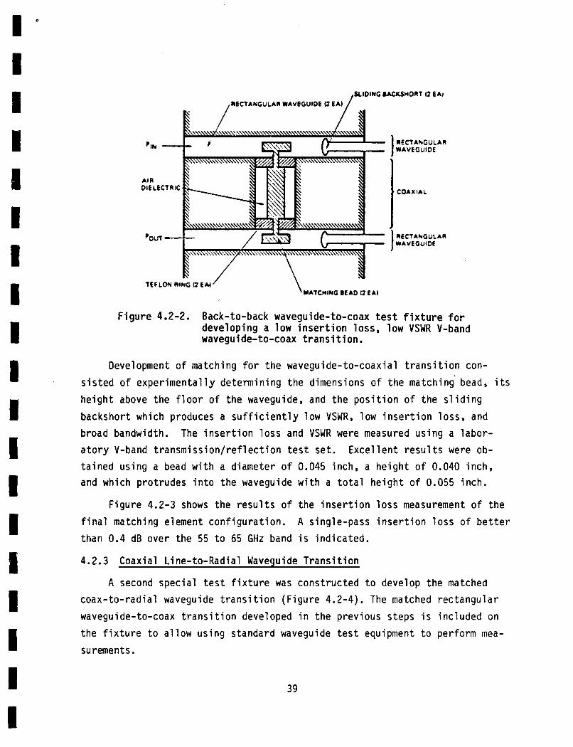
I F igu re 4.2-2. Back-to-back waveguide-to-coax t e s t f i x t u r e f o r
developing a low i n s e r t i o n loss, low VSWR V-band waveguide-to-coax t r a n s i t i o n .
Development o f matching f o r the waveguide-to-coaxial t r a n s i t i o n con-
s i s t e d o f exper imenta l l y determin ing the dimensions o f the match ing bead, i t s he igh t above the f l o o r o f the waveguide, and the p o s i t i o n o f the s l i d i n g
backshort which produces a s u f f i c i e n t l y low VSWR, low i n s e r t i o n loss, and broad bandwidth. The i n s e r t i o n l o s s and VSWR were measured us ing a l abo r - a t o r y V-band t ransmiss ion / re f l ec t i on t e s t set . Exce l len t r e s u l t s were ob- ta ined us ing a bead w i t h a diameter o f 0.045 inch, a he igh t o f 0.040 inch, and which prot rudes i n t o the waveguide w i t h a t o t a l he igh t o f 0.055 inch.
F igure 4.2-3 shows the r e s u l t s o f the i n s e r t i o n l o s s measurement o f the
f i n a l matching element con f igu ra t i on . A single-pass i n s e r t i o n loss o f b e t t e r than 0.4 dB over the 55 t o 65 GHz band i s ind ica ted .
4.2.3 Coaxial L ine-to-Radial Waveguide T r a n s i t i o n
A second specia l t e s t f i x t u r e was const ructed t o develop the matched coax- to- rad ia l waveguide t r a n s i t i o n (F igure 4.2-4). The matched rec tangu lar waveguide-to-coax t r a n s i t i o n developed i n the prev ious steps i s inc luded on
the f i x t u r e t o a l l o w us ing standard waveguide t e s t equipment t o perform mea-
surements.
39

0 4 0 E a a Y 0
0.8 0
0 c Y 0 a m vi
1.2 8
0 0 i
d z t
t c
I L , * 1.6 I a8
I I I I I I 2.0 dD f O 10 -
50 CREOUENCY IGWI
Figure 4.2-3. Insertion loss of'the V-band symnetric back-to-back waveguide-to-coax test fixture after a suitable matching bead was developed.
AIR DIELECTRIC
PARALLEL
TEFLON RING
'COAX TO.RADIAL LINE YATCUING BEAD
OF RADIAL LINE
Figure 4.2-4. Test fixture for developing a matched V-band coax-to- radial line transition. Upper section is the matched waveguide-to-coax transition previously developed.
40
1 I I I I I I 1 I 1 I 1 II I 1 1 1 I I

The p a r a l l e l p l a t e r a d i a l l i n e sec t ion i s terminated a t i t s per iphery
w i t h sect ions o f tapered microwave absorbing ma te r ia l . A s u i t a b l e conf igura-
t i o n f o r a matching bead a t the coax- to- rad ia l t r a n s i t i o n was determined t o
have a diameter o f 0.045 inch and he igh t o f 0.040 inch; the bead prot rudes i n t o the waveguide w i t h a he igh t o f 0.066 inch.
The measurement o f the r e t u r n l o s s versus frequency f o r t h i s conf igura- t i o n i s shown i n F igure 4.2-5. 55 t o 65 GHz band i s ind ica ted . A s h o r t - c i r c u i t i n g m e t a l l i c r i n g p laced w i t h i n the p a r a l l e l p l a t e r a d i a l l i n e sect ion, making contac t w i t h both the
top and bottom p a r a l l e l p l a t e s on the r a d i a l l i n e , w i l l a l l o w a measurement o f the double-pass i n s e r t i o n loss. l oss a t the waveguide p o r t when the sho r t i ng r i n g i s i n p lace w i t h i n the p a r a l l e l p l a t e r a d i a l l i n e . The single-pass i n s e r t i o n l o s s o f t h i s f i x t u r e cannot be measured d i r e c t l y because there are no p r a c t i c a l means o f d i r e c t l y
measuring the power i n the r a d i a l l i n e .
A r e t u r n l o s s o f b e t t e r than 20 dB over the
This i s performed by measuring the r e t u r n
FREOUENCV (GHzI
F igu re 4.2-5. Return l o s s f o r an opt imized V-band coax ia l - t o - r a d i a l waveguide t r a n s i t i o n t e s t f i x t u r e i n which tapered Eccosorb loads are p laced around t h e c i r - cumference of t h e r a d i a l l i n e t o te rmina te t h e r a d i a l l i n e mode.
41

The measured r e t u r n l o s s f o r t h i s c o n f i g u r a t i o n was about 1.3 dB over
the 59 t o 64 GHz frequency range. Therefore, the single-pass i n s e r t i o n l o s s
o f the c i r c u i t i s about 0.65 dB over the 59 t o 64 GHz band. observed i s t h a t t he response showed much more r i p p l e over the frequency; we be l i eve t h i s i s due t o asymmetry o f machined p a r t s and p o s i t i o n o f sho r t - c i r c u i t i n g r i n g .
One phenomenon
4.2.4 Radial Waveguide-to-N-Way Rectangular Waveguide Por t s
The i n i t i a l goal t o meet the program requirements i s t o demonstrate the power combining techniques t o combine four IMPATT diodes t o reach a power ou tpu t o f 1 W minimum. On the o the r hand, i t i s be l i eved t h a t one o f the advantages o f an N-way r a d i a l waveguide power div ider/combiner i s t o use a
l a r g e rad ius o f the r a d i a l waveguide; i.e., a l a r g e N. Therefore, a 16-way r a d i a l waveguide power div ider/combiner i s designed and f a b r i c a t e d i ns tead o f
a four-way; f o u r a m p l i f i e r s w i l l mount t o t h i s power d i v i d e r / combiner w i t h
the remaining p o r t s terminated t o demonstrate the combining techniques. This will be i l l u s t r a t e d i n the sec t i on on a m p l i f i e r i n t e g r a t i o n .
A photograph o f the f i n a l hardware i s shown i n F igure 4.2-6. The r a d i u s and he igh t o f t h i s r a d i a l waveguide a r e 0.402 and 0.074 inch, respec t i ve l y . The b lock i s made o f brass f o r ease o f machining, and i s gold-plated. S ix -
teen rec tangu la r waveguides a re machined and symmet r ica l l y d i r e c t e d r a d i a l l y outward from the center. The u n i t i s f a b r i c a t e d us ing numer ica l l y -cont ro l l e d
machining techniques, where t i g h t machining to le rances and good phys ica l sym- met ry can be c o n t r o l l e d .
The complete 16-way V-band r a d i a l waveguide power div ider/combiner ne t -
work i s cons t ruc ted by us ing the two p r e v i o u s l y matched t r a n s i t i o n elements. The impedance matching o f the r a d i a l waveguide t o the 16 symmet r ica l l y placed
rec tangu lar waveguides on the f i n a l hardware was done by symmet r ica l l y p l a c i n g a s e t o f un i fo rm d i e l e c t r i c chips near the i n t e r f a c e o f the r a d i a l waveguide and the a r r a y o f rec tangu la r waveguide.
d i e l e c t r i c ch ip matching elements i s shown i n F igure 4.2-7.
'
A close-up view o f these
Exce l l en t r e s u l t s have been achieved from the f i n a l u n i t . An i n s e r t i o n
l o s s o f 1 5 0.3 f o r the 26 power d i v i s i o n c o e f f i c i e n t s and a r e t u r n l o s s a t
the i n p u t p o r t b e t t e r than 12 dB over the 55 t o 67 GHz frequency range were measured. The average power d i v i s i o n c o e f f i c i e n t o f the 16 ou tpu t p o r t s i s
I 42
" 1 I I 1 1 I I I I
. I I 1 I 1 I I 1 I I

F igu re 4.2-6. 16-way V-band r a d i a l l i n e d iv ider /combiner network.
F igu re 4.2-7. Close-up view o f d i e l e c t r i c c h i p matching elements.
p l o t t e d versus frequency i n F igure 4.2-8.
p u t p o r t s i s k0.6 dB, and i s p robab ly a r e s u l t o f imper fec t ions i n the
machining o f t he u n i t and/or o f the matching elements.
t he r e t u r n l o s s o f the i n p u t p o r t and a t y p i c a l ou tpu t p o r t o f t h i s network.
I s o l a t i o n c o e f f i c i e n t s between ou tpu t p o r t s have a l s o been measured; t he
The power imbalance over the ou t -
F igure 4.2-9 shows
43

1
1:
J Ip 1:
5 B I 2 14
-I
c
16
0 I 1
I
0 to 0
Ideal 16-Way Power Divider/Combiner
I I I
Figure 4.2-8. Measured transmission loss from the
- m -0
VI VI 0 2
E 0 * L 0) VI E
v
.r
w
7
m E 0
+-' -0 -0 4
.r
.r
input ( comnon 1
Output Port Input Port 4 f g 1s
2s 6 4 6 6 6 8 6 0 6 Z M 0 6 6 (
FREQUENCY (GHz)
Figure 4.2-9. Return loss o f both input (comnon) port and a typical output (radial) port on the 16-way radial waveguide power divider/combiner.
44
1 I 1 I 1 I I J 1 I I 1 1 1 1 I I I I

lowest i s o l a t i o n i s observed between d i r e c t l y opposing ou tpu t po r t s . o f t he measurements of t he i s o l a t i o n c o e f f i c i e n t s o f t h i s power divider/com- b i n e r a re presented i n F igure 4.2-10.
Resul ts
0 I I
6
I I I
FREQUENCY ( C W
. F i g u r e 4.2-10. I s o l a t i o n between ou tpu t p o r t s on t h e 16-way r a d i a l waveguide power div ider/combiner (a) p o r t s 1-2, 1-3, 1-4, and 1-5; (b) p o r t s 1-6, 1-7, 1-8, and 1-9.
The r a d i a l l i n e combiner as designed i s a l oss less s t ruc tu re ; i.e., t he re a re no te rmina t ions i n the network t o suppress h igher -order modes w i th - i n r a d i a l waveguide which has c i r c u m f e r e n t i a l (@) v a r i a t i o n . Consequently,
t h i s network does n o t p rov ide h igh p o r t - t o - p o r t i s o l a t i o n , which i s requ i red f o r power combining IMPATT power a m p l i f i e r s . Poor i s o l a t i o n can be improved by us ing ex terna l c i r c u l a t o r s . A c o n f i g u r a t i o n f o r an IMPATT a m p l i f i e r power combiner scheme, us ing a p a i r o f r a d i a l l i n e s and combining the power o f 16 matched two-port c i r cu la to r - coup led a m p l i f i e r modules, i s shown schemat ica l l y
i n F igure 4.2-11. A rep resen ta t i ve c o n f i g u r a t i o n sketch o f the ac tua l hard-
ware f o r such a u n i t i s shown i n F igure 4.2-12.
I n t h i s con f igu ra t i on , each o f the 16 two-port c i r cu la to r - coup led ampl i - f i e r modules has an i s o l a t o r (i.e., a terminated c i r c u l a t o r ) on the i n p u t and
45

INPUT +-
- MODULE NO 1
Figure 4.2-11. Module-level power combining of N two-port reflection amplifiers by means of a pair of N-way divider/combiner networks. replaced by N amplifier chains o f stages.
Generally, N single-stage' amplifiers can be
46

TOP VIEW
2-PORT AMPLIFIER 16.WAY RADIAL LINE DIVIDER
\ INPUT WAVEGUIDE PORT \ MODULE 1 OF 16
WAVEGUIDE TERMINATION
REFLECTION 4MP OUTPUT WAVEGUIDE PORT
SIDE VIEW / 3JUNCTlON CIRCULATOR WAVEGUIDE
TE AMINATION
Figure 4.2-12. Conceptual design of 16-way radial line module-level power combiner configuration.
the output sides of each module. high degree of module-to-module isolation, which an N-way divider/ combiner network alone generally could not provide.
This is required to provide low VSWR and a
TRW's V-band circulators have an isolation of about 25 dB over a wide Since there are two circulator passes on the input and (6 GHz) bandwidth.
output sides of each amplifier module, this configuration provides at least 50 dB of module-to-module isolation. by external ferrite components, is an outstanding advantage of the radial line power combiner.
This high degree of isolation, provided
47

Radial waveguide power divider/combiners using higher-order modes have also been considered; such schemes offer some very a t t rac t ive features:
1) Higher-order modes, par t icular ly c i rcular e l ec t r i c TE mode of a r ad ia l waveguide, provide low loss and h i g h powe?”propagation character is t ics .
2) The E-field polarization o f the ci rcular e l ec t r i c mode i s i n the direction, making i t easier t o implement mode suppressions w i t h i n the network.
3 ) Again, due t o f i e ld polarization, the a d d i t i o n a l waveguide twists for the previous power combining technique can be eliminated. conceptual conf igura t ion of the power mode i s shown i n Figure 4.2-13.
In summary, TRW has developed a novel wideband power divider/combiner
A
network d u r i n g the present program period. waveguide as a basic transmission medium.
This network uses the rad ia l For a 16-way radial waveguide
power divider/combiner, an bet ter than 12 dB have been This power divider/combiner power combining solid s t a t e nas. To power combine IMPA external f e r r i t e components isolation.
nsertion loss of less t h a n 1.0 dB and return loss obtained over a frequency range of 55 t o 67 GHz. network is suitable for applications such as amplifier modules a s well a s phased array anten- T amplifier modules, i t will be necessary t o use t o o b t a i n suff ic ient ly h i g h modu 1 e-to-modul e
4.3 WIDEBAND, LOW LOSS CIRCULATORS
The three-port c i rculator i s one essential component found i n most i n - jection-locking osc i l la tors or reflection amplifiers employing IMPATT diodes. The circulator decouples the i n p u t c i r cu i t from the o u t p u t c i r cu i t and , i n e f fec t , transforms a one-port network i n t o one w i t h two ports. Since both the i n p u t and o u t p u t signals are transmitted th rough the circulator , the electr ical character is t ics of the ci rculator have a profound influence on overall c i r cu i t performance. The requirements imposed on the circulators used i n the proposed program are stringent. They must be capable of h a n d l i n g the signal power and have a wide bandwidth ( w i t h low SWR) for proper c i r cu i t operations, and an adequate isolation for i n p u t / o u t p u t decoupling. Moreover, the circulators must have an extremely low insertion loss ( i n the vicini ty of 0.3 dB) so as n o t t o further degrade the relat ively poor efficiency of IMPATT devices. TRW has developed and patented such h i g h performance circulators .
48
1
I I 1 1 1 J I
I 1 I I 1 I I 1 I
m
a

TOP VIEW
0 16-WAY RADIAL LINE DIVIDER INPUT WAVEGUIDE PORT
2-PORT AMPLIFIER MOOULE 1 OF 16
WAVEGUIDE TE W INAT ION
I
REFLECTION AMPLIFIER L 1 J
1 1
I 16-WAY RADIAL
I
LINE COMBINER WAVEGUIDE 3-JUNCTION TE WINAT ION CIRCULATOR
mycL. OUTPUT WAVEGUIDE PORT i
SIDE VIEW
Figure 4.2-13. Conceptual design o f radial line power combiner using circular electric TEO1 wave.
49
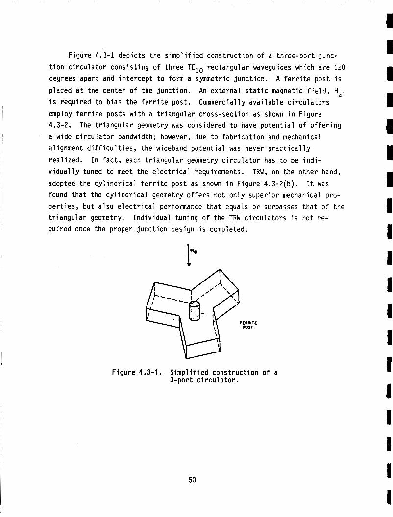
Figure 4.3-1 dep ic t s the s i m p l i f i e d c o n s t r u c t i o n o f a t h ree -po r t junc- t i o n c i r c u l a t o r c o n s i s t i n g o f t h ree TEIO rec tangu la r waveguides which a re 120 degrees apar t and i n t e r c e p t t o form a symmetric j unc t i on .
p laced a t the cen te r o f the j u n c t i o n . An ex te rna l s t a t i c magnetic f i e l d , Ha, i s requ i red t o b ias the f e r r i t e post. Commercially a v a i l a b l e c i r c u l a t o r s employ f e r r i t e posts w i t h a t r i a n g u l a r c ross-sec t ion as shown i n F igure 4.3-2. a wide c i r c u l a t o r bandwidth; however, due t o f a b r i c a t i o n and mechanical
al ignment d i f f i c u l t i e s , the wideband p o t e n t i a l was never p r a c t i c a l l y
rea l i zed . I n fac t , each t r i a n g u l a r geometry c i r c u l a t o r has t o be i n d i -
v i d u a l l y tuned t o meet the e l e c t r i c a l requirements. adopted the c y l i n d r i c a l f e r r i t e pos t as shown i n F igure 4.3-2(b) . found t h a t the c y l i n d r i c a l geometry o f f e r s n o t o n l y super io r mechanical pro- p e r t i e s , b u t a l s o e l e c t r i c a l performance t h a t equals o r surpasses t h a t o f t he t r i a n g u l a r geometry.
A f e r r i t e pos t i s
The t r i a n g u l a r geometry was considered t o have p o t e n t i a l o f o f f e r i n g .
TRW, on the o the r hand,
It was
I n d i v i d u a l t un ing o f t he TRW c i r c u l a t o r s i s n o t re -
I qu i red once the proper j u n c t i o n design i s completed.
F igu re 4.3-1. S i m p l i f i e d c o n s t r u c t i o n o f a 3 -por t c i r c u l a t o r .
50
1 I 1 1 II I I I I 1 I 1 I I I 1 I 1 I

F i g u r e 4.3-2. Comparison o f convent ional t r i a n g u l a r and TRW's cy1 i n d r i c a l c i r c u l a t o r j unc t i ons .
A d e t a i l e d graphic rep resen ta t i on o f the TRW c i r c u l a t o r j u n c t i o n i s de-
p i c t e d i n F igure 4.3-3. e l e c t r i c spacers, and a d i e l e c t r i c tube enc los ing the above pa r t s . j u n c t i o n assembly i s nested i n m e t a l l i c t rans former d i scs indexed p r e c i s e l y i n the c i r c u l a t o r housing formed by th ree i n t e r s e c t i n g waveguides. a t i o n o f a j u n c t i o n c i r c u l a t o r i s bes t explained w i t h the a i d o f Figures 4.3-4(a) and ( b ) . guides behaves as a TMl10 mode c y l i n d r i c a l c a v i t y .
n e t i c b i a s Ha i s removed and the c a v i t y i s e x c i t e d b y the TE waveguide, the r e s u l t i n g TMl10 f i e l d p a t t e r n i s o r i e n t e d i n the d i r e c t i o n shown i n F igure 4.3-4(a). no f e r r i t e pos t i s present. the p a t t e r n o r i e n t a t i o n i s as fo l l ows . I n the absence o f an ex te rna l mag-
n e t i c bias, the electromagnet ic l e f t and r i g h t p o l a r i z e d waves e x i s t i n g i n -
s ide the f e r r i t e have the same propagat ion constant. The two waves emerge from the f e r r i t e in-phase, and no r o t a t i o n of t he c a v i t y f i e l d p a t t e r n takes
place. As shown i n F igure 4.3-4(a), the presence o f e l e c t r i c and tangen t ia l
The j u n c t i o n cons is t s o f one f e r r i t e d isc , two d i - This
The oper-
Not ice t h a t the synmetric j u n c t i o n formed by the wave-
When the ex te rna l mag-
wave from one
The p a t t e r n o r i e n t a t i o n i s i d e n t i c a l t o t h a t when
10
The reason t h a t the f e r r i t e pos t does n o t change
51

FERRITES MATCHlNG 'TRANS ORMERS
OlELECTRlC SLEEV
F igu re 4.3-3. Graphic p resenta t 'on \ of TRW's c i r c u l a t o r j u n c t i o n .
(B) W I T H MAGNETIC BIAS Ha ( A ) WIM NO MAGNETIC BIAS
F i g u r e 4.3-4.
magnetic f i e l d s a t the waveguide-cavity i n t e r f a c e a l lows e x c i t a t i o n o f t he
TE
F i e l d p a t t e r n f o r H-plane waveguide c i r c u l a t o r us ing TMl10 mode.
wave i n the two ou tpu t waveguides.
When the ex terna l magnetic b ias , Ha, i s appl ied, the s i t u a t i o n i s 10
changed. The two p o l a r i z e d waves i n the f e r r i t e no longer have the same pro- pagat ion constant, r e s u l t i n g i n r o t a t i o n of the mode p a t t e r n o f the c a v i t y by
30 degrees, as shown i n F igure 4.3-4(b). pu t waveguide stays unchanged, w h i l e the remaining waveguide i s i s o l a t e d
The f i n a l outcome i s t h a t one ou t -
52
4 I 1 I I 1 I 1 I I I 1 I I I 1 1 1 1

( i .e . , no o u t p u t ) .
a r e no e l e c t r i c and t a n g e n t i a l magnetic f i e l d s a t t h e waveguide-cavi ty i n t e r -
face t o e x c i t e t h e TEIO wave i n the i s o l a t e d waveguide.
band c i r c u l a t o r . curve, i n s e r t i o n l o s s data.
l a t o r has a passband from 59 t o 62 GHz, a bandwidth o f 3 GHz. loss i n t h e passband i s l e s s than 0.5 dB.
l a t o r i s f u r t h e r enhanced by var ious housing designs. F i g u r e 4.3-6 shows t h e c i r c u l a t o r c o n s t r u c t i o n u s i n g a m u l t i p l e j u n c t i o n housing. Successful assem-
b l y o f t h e m u l t i p l e j u n c t i o n housing i s p r i m a r i l y due t o t h e r e p e a t a b i l i t y o f
the c y l i n d r i c a l j u n c t i o n c i r c u l a t o r developed a t TRW. F igure 4.3-6 houses t h r e e c i r c u l a t o r j u n c t i o n s . were used i n t h e c o n s t r u c t i o n o f t h e V-band a m p l i f i e r .
power stage a m p l i f i e r modules r e q u i r e d one each o f these assemblies.
end c i r c u l a t o r s a re used as i s o l a t o r s t o achieve t h e necessary p o r t - t o - p o r t
i s o l a t i o n r e q u i r e d by the r a d i a l l i n e combiner.
The c a v i t y f i e l d p a t t e r n has a l t e r e d so much t h a t t h e r e
F igure 4.3-5 i n d i c a t e s t h e e l e c t r i c a l performance o f a t y p i c a l TRW V-
The upper curve represents t h e SWR data and t h e lower I t can be seen t h a t f o r a SWR o f 1.2, t h e c i r c u -
The i n s e r t i o n
The a p p l i c a b i l i t y o f the c i r c u -
The assembly shown i n S i x assemblies o f t h i s t y p e
Each o f the f o u r
The two
0.0 dB ' 0.5 d 0 1
ISOLATION AND RETURN LOSS OF ONE JUNCTION
-20 dB -22 dB
1.0 6- .
\
I -
LL - --.-------- A F i g u r e 4.3-5. Swept frequency response of a t h r e e - j u n c t i o n c i r c u l a t o r .
53

F i g u r e 4.3-6. Th ree - junc t i on c i r c u l a t o r assembly.
The implementat ion o f t h i s m u l t i p l e j u n c t i o n c i r c u l a t o r has g r e a t l y sim-
p l i f i e d the i n t e g r a t i o n of t he r a d i a l l i n e combiner.
waveguide c i r c u l a t o r j u n c t i o n s have been assembled i n t o one compact assembly,
t h e o v e r a l l dimensions o f t he a m p l i f i e r have been reduced. Second, the e l e c -
t r i c a l pa th l e n g t h through the i s o l a t o r - c i r c u l a t o r - i s o l a t o r network over the
opera t i ng f requency i s i d e n t i c a l from housing-to-housing because no i n t e r c o n - n e c t i n g waveguide sec t i ons a re r e q u i r e d t o b o l t t he va r ious components t o -
gether, and because each c i r c u l a t o r j u n c t i o n i s i d e n t i c a l . No a d d i t i o n a l
d i e l e c t r i c t u n i n g ch ips a re necessary i n t h e i r assembly. It i s e s s e n t i a l t o the opera t i on of t he r a d i a l l i n e combiner t h a t t he power e n t e r i n g each o f t h e
combiner arms i s i n phase across the f requency o f i n t e r e s t . Any phase e r r o r between power module arms w i l l degrade the o v e r a l l performance o f t he ampl i - f i e r .
F i r s t , because these
54
1 I I 1 1 I I 1 I I I 1 I I I I I I I

4.4 SILICON IMPATT DIODE DEVELOPMENT
Development o f V-band s i l i c o n IMPATT diodes was funded i n p a r t by an i n -
t e r n a l research program a t TRW, and was n o t a con t rac tua l task i n developing t h i s r a d i a l l i n e combiner. It i s , however, an impor tan t subject , and we w i l l r e p o r t i t s achievements.
The IMPATT diode i s shown schemat ica l l y i n F igure 4.4-1. It con- s i s t s o f a h e r m e t i c a l l y sealed ceramic r i n g package on a copper d isk , w i t h the diode c h i p thermal compression-bonded on a Type I I - A diamond heats ink f o r
e f f i c i e n t heat d i s s i p a t i o n .
i n t o a 0.060-diameter copper d isc . E l e c t r i c a l con tac t t o the diode mesa i s provided b y a go ld r i bbon which prov ides the proper s e r i e s inductance (=0.12 nH) t o the diode mesa, as shown i n the equ iva len t c i r c u i t o f F igure 4.4-2. The diodes are tes ted as o s c i l l a t o r s us ing the t e s t setup shown schemat ica l l y i n F igure 4.4-3.
i s g iven i n F igure 4.4-4. I n rev iewing these histograms, we f i n d t h a t a t a
j u n c t i o n temperature o f 250°C, 86 percent o f t h e diodes tes ted produced a t
l e a s t 28 dBm ( o r 2 7 9 4 mW). The power budget was determined f o r t h i s ampl i - f i e r from these r e s u l t s ( r e f e r t o Sect ion 3.5).
The diamond heats ink i s g o l d p l a t e d and pressed
The copper d i s c i s then soldered onto a copper heatsink.
A h istogram showing the r e s u l t s o f f o u r diode l o t s f a b r i c a t e d i n 1984
F igu re 4.4-1. IMPATT diode package.
55

Figure 4.4-3. Block diagram of diode test station.
56
r-- I
1 I I I I I
a I I I - J
1 CACKAGED DIODE
I I
WHERE -R IS THE NEGATIVE RESISTANCE C, IS THE JUNCTION CAPACITANCE
L, IS THE PACKAGE INDUCTANCE
C, IS THE PACKAGE CACACITANCE
RL IS THP TRANSFORMED LOAD IMPEDANCE
Figure 4.4-2. Schematic diagram o f an IMPATT diode and its package parasi tics.
METER 7 I YlfW
VAR Am
SWEEP GENERATOR
...-.. m E R TERMlNAllOh
rH*. PAD I
METER ANALYZER

30
25
20
15 VI
# E! 0
Y 0
w a
10 z
5
1% 1%
TRY V-BAND SIL ICON IMPATT OIOOE RF TEST RESULTS
N W E R OF DIODES TESTEO:79 MXIW JUNCTION TEMPERATURE RISE: 220'C
.25- .32 .32- .40 .40 -.50 .50 - .63 .63- .79
PWER (HATTS)
28% -
- ' 9 - 1.c 0 - 1 . 3 L, 3 - 1 . 6 1 . 6 - 2 . 0
F igu re 4.4-4.
Extensive development o f TRW's 60-GHz s i l i c o n d o u b l e - d r i f t IMPATT diodes
Typ ica l TRW s i l i c o n IMPATT diode t e s t r e s u l t s .
began i n 1981. The pr imary goal of t h i s e a r l y e f f o r t was t o produce a h i g h power V-band diode. diode l o t s which cou ld produce 1 W of RF power. program t h a t the diodes used produce t h e i r maximum power a t 60.0 GHz w i t h an
e f f i c i e n c y grea ter than 6 percent and a j u n c t i o n temperature l e s s than 250°C. The added c o n s t r a i n t s on the diode opera t iona l requirements demanded f u r t h e r diode development. We had the c a p a b i l i t y t o produce a h ighe r power IMPATT diode, b u t now the diode had t o be opt imized f o r maximum performance a t a se lec ted frequency, 59 t o 61.5 GHz.
Eva lua t ing the diode as o s c i l l a t o r s revea led several
It was essen t ia l f o r t h i s
Opt im iza t ion of the IMPATT diode was accomplished i n two steps. The f i r s t was t o op t im ize the d i f f u s i o n p r o f i l e o f the diode ch ip and the second,
57

t o op t im ize the package p a r a s i t i c s t o the p a r t i c u l a r p r o f i l e s .
was t o produce a h igh power, h igh e f f i c i e n c y , 60-GHz diode. diode r e s u l t s revealed a c o n s i s t e n t l y h igh opera t iona l frequency, approx- i m a t e l y 66 GHz. Because o f t h i s h i g h o s c i l l a t i o n frequency, t he d r i f t r e g i o n of the diodes was lengthened.
ad jus ted i n an e f f o r t t o improve device e f f i c i e n c y . Dur ing 1983 and 1984, 26
V-band IMPATT diode wafers were f a b r i c a t e d and RF evaluated.
l o t s , t he re were 75 separate diode d e l i v e r i e s t o t a l i n g 594 i n d i v i d u a l diodes.
Each diode was t e s t e d f o r i t s DC c h a r a c t e r i s t i c s , thermal res is tance, and RF performance. For every diode, t h e RF eva lua t i on consiste! o f an average o f
s i x adjustments i n t h e coax ia l shims, o r b i a s p ins , i n a d d i t i o n t o numerous adjustments i n DC opera t ion l e v e l s , choke, and backshort p o s i t i o n s . RF eva lua t i on i s t h e most ted ious and t ime consuming process. f o r t we have achieved the t e s t r e s u l t s shown i n Table 4.4-1.
The o b j e c t i v e
Previous V-band
I n add i t i on , t he dopant concent ra t ions were
From these 26
C lea r l y ,
From t h i s e f -
9. a
10.0
9.5
Table 4.4-1. V-band s i l i c o n IMPATT diodes bes t t e s t r e s u l t s .
2.00
1.66'
1.15
H I CH EST POWER DIODE
HIGHEST EFFl C I ENCY DIODE
HIGHEST POWER AND HI CH EST EFFICIENCY DIODE
DIODE NO.
112E-1
112E-1
109B-1U
ATAT; < 215OC
FREQUENCY = 60 CHz TA = 25OC
~ ~~~ I POWER EFFICIENCY (W)
~ ~~ ~
FREQUENCY
53.12
53.35
61.1
335
272
181
The IMPATT diodes used i n t h i s program were se lec ted from th ree l o t s f o r t h e i r RF power c a p a b i l i t y a t a g iven j u n c t i o n temperature.
diode
Tab1 e 4.4-2 presents t e s t r e s u l t s f o r each of the seven d e l i v e r e d diodes a t the opera t ing c u r r e n t l e v e l used i n the de l i ve red a m p l i f i e r .
sa
I I I I 1 I I I 1 I I I I I 1 I I 1 I

*RESULTS ARE GIVEN A T THE SAME CURRENT LEVELS USED IN THE DELIVERED AMPLIFIER.
Table 4.4-2. IMPATT diode oscillator test results for the seven delivered diodes.
DIODE NO.
109A6 109813 109B9 11261 11262
l l2G6 113A1
vOP 26.9 23.5 26.7 28.7 29.3
29.2 27.7
I * OP
500 250 600 500
375
450 500
f
66.90 56.00 59.98 59.18 61.04 59.62 60.32
- 28.6 22.0 29.7 30.1 29.9
30.3 29.2
T. I - I POS IT I ON
DRIVER STABLE
DRIVER STABLE
DRIVER ILO
POWER MODULE ILO
POWER MODULE ILO
POWER MODULE 110
POWER MODULE 110
59
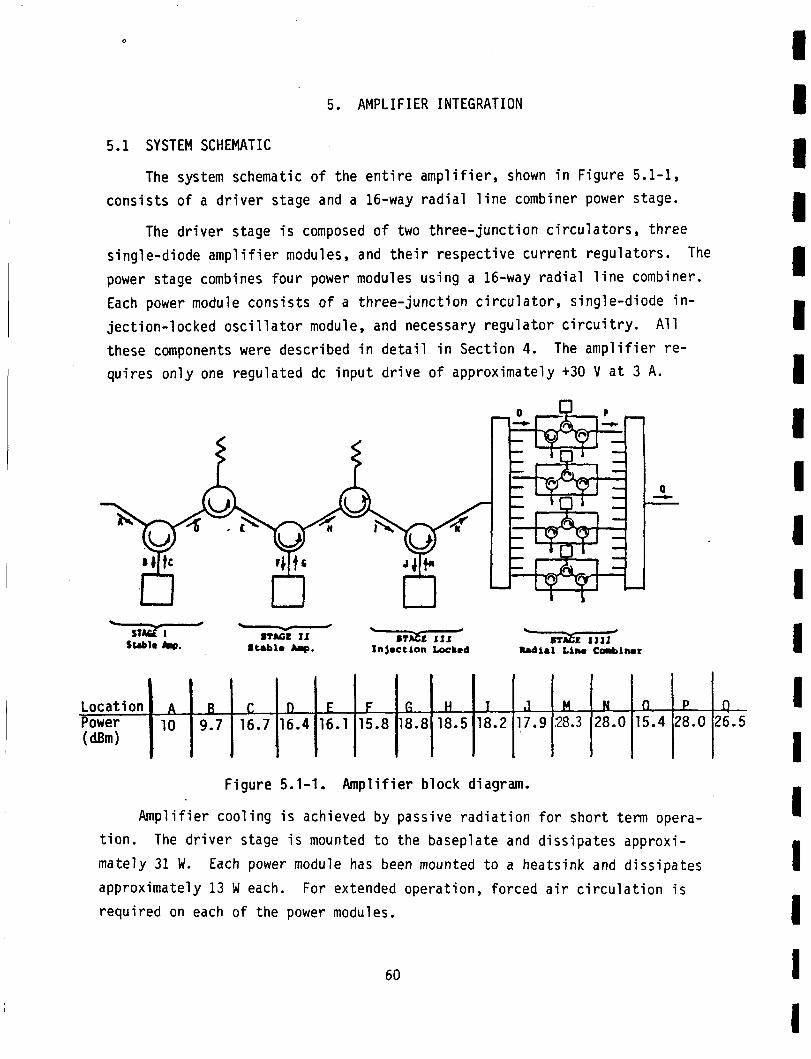
5. AMPLIFIER INTEGRATION
Location A 0 C D E F G H 1 J M N 0 Power 10 9.7 16.7 16.4 16.1 15.8 18.8 18.5 18.2 17.9 28.3 28.0 15.4 ( a m )
5.1 SYSTEM SCHEMATIC
P 0 28.0 26.5
The system schematic of the entire amplifier, shown in Figure 5.1-1, consists of a driver stage and a 16-way radial line combiner power stage.
The driver stage is composed of two three-junction circulators, three single-diode amplifier modules, and their respective current regulators. power stage combines four power modules using a 16-way radial line combiner. Each power module consists of a three-junction circulator, single-diode in- jection-locked oscillator module, and necessary regulator circuitry. these components were described in detail in Section 4. quires only one regulated dc input drive of approximately +30 V at 3 A.
The
All The amplifier re-
n
Figure 5.1-1. Amplifier block diagram.
Amplifier cooling is achieved by passive radiation for short term opera- The driver stage is mounted to the baseplate and dissipates approxi-
Each power module has been mounted to a heatsink and dissipates For extended operation, forced air circulation is
tion. mately 31 W. approximately 13 W each. required on each o f the power modules.
8 B I I 1 I I I I I I I I 1 I I 1 I I
60

5.2 INTERFACE REQUIREMENTS
Both RF i n p u t and ou tpu t connectors a re v i a standard WR-15 waveguide w i t h a MIL-F-3922/67B-008 f lange. The i n p u t RF s igna l should be o f a s i n g l e frequency w i t h i n the range o f 59.2 t o 60.7 GHz and n o t exceed 0.03 W cw. a standard banana jack a t +32 V ( red ) and ground (b lack ) .
5.3 AMPLIFIER EVALUATION
Both the source and load SWR should n o t exceed 1.3:l.
DC i n p u t t o t h e u n i t i s connected through
The a m p l i f i e r f o r t h i s program was developed i n stages and l a t e r assembled i n t o i t s f i n a l con f i gu ra t i on . the a m p l i f i e r w i l l be discussed
gor ized as fo l l ows :
0 Stab le a m p l i f i e r d r i v e r 0 Single-diode i n j e c t i o n
e s t r e s u l t s o f the bas i c stages which c o n s t r u c t i n d e t a i l below. These bas ic stages a re cate-
p a i r ocked o s c i l l a t o r (ILO) d r i v e r ou tpu t stage.
0 Radial l i n e div ider/combiner 0 Power module ( f o u r each) 0 Bias c i r c u i t r y (seven each).
The goal o f t h i s program was t o develop a s o l i d s t a t e a m p l i f i e r w i t h t h e
f o l l o w i n g RF performance:
0 Power ou t 1 W (minimum) 0 Dynamic RF band 59 t o 61.5 GHz 0 RF ga in 17 dB
The o n l y t e s t requ i red t o determine these s p e c i f i c a t i o n s i s a power measure-
ment. e l i m i n a t e any v i s u a l spec t ra l noise. The t e s t setup used f o r a m p l i f i e r mea- surements i s schemat ica l l y represented i n F igure 5.3-1.
5.4 STABLE AMPLIFIER DRIVER PAIR
No noise measurements were conducted, b u t the a m p l i f i e r was tuned t o
The f i r s t two a m p l i f i e r modules w i t h i n the d r i v e r sec t i on a re s t a b l e
a m p l i f i e r s due t o the low i n p u t d r i v e l e v e l ava i l ab le . I n j e c t i o n - l o c k e d modules a t t h i s l o c a t i o n would p robab ly produce too narrow a bandwidth. c o n f i g u r a t i o n o f t h i s s t a b l e a m p l i f i e r stage, shown i n F igure 5.4-1, cons i s t s o f two c i r c u l a t o r j unc t i ons , one i s o l a t o r , and two a m p l i f i e r s . presents a po in t -by-po in t response of the two cascaded s t a b l e a m p l i f i e r s .
The
F igure 5.4-2
61
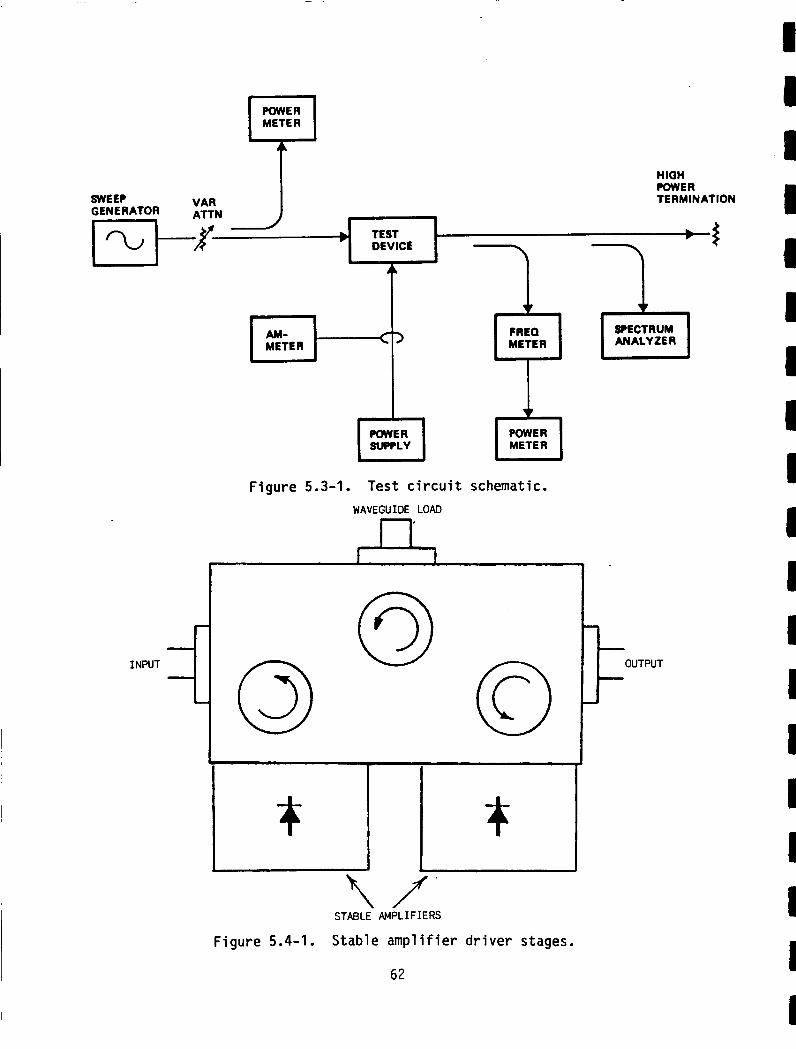
METER 0
*
HlOH POWER TERMINATION
I
- L L
SWEE? GENERATOR
i INPUT
4 TEST DEVICE
t METER -I
$1 SUPPLY
METER 9 $1 METER
Figure 5.3-1. Test circuit schematic. WAVEGUIDE LOAD n
0 8 0 STABLE- AMPLIFIERS
Stable amplifier driver stages. Figure 5.4-1.
62
SPECTRUM ANALYZER
1 OUTPUT F
I I 4 1 4 I I l I I I I I I I I 1 I I
140.0Q
2 120.0c3 E
Q! 100.0Q W x 0 a 80.UEl I- 3 n
60.QO E;
4 0. E3E3
r 'STABLE AMPLIFIER DRIVER STAGES - - - -
*-- -/+-e - - Curve #1 I n p u t Power = 10.0 mW
#2 = 12.6 mW #3 = 15.8 mW -
- #4 = 17.4 mW
0.QO I - -11 1 I I 1 I
FREQUENCY ( GHz 1 F igu re 5.4-2. Swept frequency response o f t h e two-stage
stab1 e amp1 i f i e r d r i v e r . This method of record ing was chosen over a swept response due t o the r i p p l e o f our sweeper source. The t y p i c a l ga in f o r t h i s a m p l i f i e r p a i r i s about 9
dB w i t h a +1 dB r i p p l e . There i s evidence o f ga in compression a t about 60.25
GHz f o r d r i v e l e v e l s above 12 dBm. This compression does n o t s i g n i f i c a n t l y a f f e c t the o v e r a l l performance of t h e a m p l i f i e r . F igu re 5.4-2 does n o t imply t h a t the bandwidth o f t h i s stage i s reduced a t the h ighe r d r i v e l e v e l s . Simply, the sweeper used f o r t h i s measurement was l i m i t e d i n i t s ou tpu t power c a p a b i l i t y . We w i l l assume a constant d r i v e l e v e l o f 10 dBm a t the i n p u t p o r t o f the amp- l i f i e r . Minor v a r i a t i o n s from t h i s d r i v e l e v e l w i l l normal ly a l t e r o n l y the bandwidth o f the o v e r a l l a m p l i f i e r .
then ab le t o t e s t the ILO d r i v e r ou tpu t stage.
The sweeper bandwidth i s narrower a t the h ighe r ou tpu t l e v e l s .
Using t h i s s t a b l e a m p l i f i e r , we were
63

5.5 ILO DRIVER OUTPUT STAGE
The l a s t a m p l i f i e r o f t he d r i v e r cha in i s an i n j e c t i o n - l o c k e d os-
c i l l a t o r . We chose the ILO a m p l i f i c a t i o n method because o f i t s h igh gain,
h igh power c a p a b i l i t i e s . F igure 5.5-1 presents a schematic o f t h i s stage,
which cons is t s o f two i s o l a t o r s on e i t h e r s i d e o f a c i r c u l a t o r at tached t o the ILO housing. p l o t t e d i n F igure 5.5-2 f o r an i n p u t d r i v e l e v e l o f 50 mW. losses due t o bo th i s o l a t o r s and the c i r c u l a t o r . l o c k i n g bandwidth o f 1.6 GHz w i t h a ga in o f approximately 11.4 ? 0.33 dB.
F igure 5.5-3 r e l a t e s the normalized bandwidth o f the ILO t o i t s gain. ILO a m p l i f i e r , t he expression r e l a t i n g the normalized bandwidth t o i t s g a i n can be approximated w i t h the f o l l o w i n g expression (assuming t h a t Po >> Pi).
The frequency versus power r e l a t i o n s h i p o f t h i s ILO i s Th is inc ludes the
From t h i s graph we f i n d a
For an
where Qext i s t he ex te rna l q u a l i t y o f the c i r c u i t .
through the measured p o i n t s on F igure 5.5-3 obeys the above expression and
i n d i c a t e s an ex te rna l Q f o r t he c i r c u i t t o be Qext = 15, which i s considered a r e l a t i v e l y low value. N o t e ' t h a t an ex te rna l Q = 15, and a ga in o f 11.4 dB def ines a locked bandwidth o f over 2 GHz. This 2-GHz bandwidth i s n o t re - f l e c t e d i n F igu re 5.5-2 due t o a drop i n the ou tpu t power l e v e l a t the band edges. We s e t the ou tpu t r i p p l e a t the 1/3-dB l e v e l i n F igure 5.5-2, which y i e l d s the 1.6-GHz bandwidth.
A s t r a i g h t l i n e drawn
5.6 RADIAL LINE COMBINER/DIVIDER
The key element t o t h i s a m p l i f i e r program i s the r a d i a l l i n e combiner Sect ion 4.2 presented a d e t a i l e d ana lys i s o f the r a d i a l l i n e and d i v i d e r .
and i t s p o r t - t o - p o r t i s o l a t i o n , i npu t - to -ou tpu t i n s e r t i o n loss, and SWR mea- surements. For optimum i n t e g r a t i o n o f a p e r f e c t l y symmetric r a d i a l l i n e power combiner, the power en te r ing the r a d i a l l i n e from each o f the 16
r a d i a l l y d i r e c t e d p o r t s must be equal i n ampl i tude and phase a t each f r e - quency.
fec t r a d i a l l i n e network, the ampl i tude and phase d i f f e r e n c e from the c e n t r a l i n p u t p o r t t o each o f the 16 r a d i a l waveguide p o r t s must be determined and corrected. Th is measurement must be performed f o r bo th the d i v i d e r network and combiner network.
To o b t a i n t h i s optimum opera t ing c o n d i t i o n us ing an ac tua l , imper-
64
I I 1 I I I 1 1 1 I I I I I I I I I 1

< INFUT
1
WAVEGUIDE LOADS
e00.00
700.00
600.00 A
-
u k--F-k - -
0 0 OUTPUT k
x Y E 500.00
. Input Driver Level 50 mW
y 400.8c) 0 0
300. OE)
I 208.00
100.00
0.00 --I - “ “ ‘ I , I I I , , ,
f REOUENCY ( G H t )
Figure 5.5-2. Swept frequency response of the driver ILO.
65

I GAIN
F i g u r e 5.5-3. Normalized bandwidth vs g a i n f o r t h e d r i v e r stage ItO.
The i d e a l method f o r t h i s type o f phase and ampli tude balance measure-
ment would use an automatic vec to r network analyzer. Although such analyzers
a re ava i l ab le , the c o n f i g u r a t i o n o f t he 16-por t d iv ider/combiner makes i t i n - compatible w i t h our present network analyzer system. This i s because each o f t he 16 ou tpu t p o r t s i s o r i e n t e d i n 16 d i f f e r e n t d i r e c t i o n s i n r e l a t i o n t o the i n p u t po r t , the c e n t r a l p o r t on the top o f the d i v i d e r . Using the present network analyzer, i t i s n o t poss ib le t o bend a waveguide each t ime t o examine
each o f the 16 ou tpu t po r t s .
A network analyzer w i t h a downconverter on the end o f a f l e x i b l e coax ia l l i n e on the i n p u t arm has been developed b u t i s no t p r e s e n t l y a v a i l a b l e a t V- band. Therefore, an a l t e r n a t e method of determining the r e l a t i v e phase o f
each ou tpu t p o r t i n re fe rence t o one another was devised.
sures the r e t u r n l o s s o f the top p o r t ( d i v i d e r i n p u t p o r t ) over frequency
w i t h each o f the 16 r a d i a l waveguides terminated us ing a matched load. The swept r e t u r n l o s s o f the s igna l f o r t h i s case shows a matched c i r c u i t ; i .e. , low VSWR.
This method mea-
Replacing one of the 16 matched te rmina t ions w i t h an ad jus tab le
I I I I I
1 I I I I I I I I 1 I
66

shor t w i l l change the swept r e t u r n l o s s measurement so the p l o t o f r e t u r n
l oss versus frequency has a c h a r a c t e r i s t i c shape; and, i n f a c t , has a c l e a r l y
de f ined resonance w i t h i n band.
and out, the resonant sp ike t r a n s l a t e s h igher and lower i n frequency, respec-
t i v e l y . The p o s i t i o n o f the back sho r t can be adjusted f o r each o f the 16 por ts , so they a l l r e s u l t i n almost the same c h a r a c t e r i s t i c r e t u r n l o s s curve versus frequency (F igure 5.6-1).
As the p o s i t i o n o f t he sho r t i s ad justed i n
59.3
FREQUENCY 60.1 60.9
m m 0 -1
U E _ - _ _ _ - - - - - - - - Y a
-25 dB
F igu re 5.6-1. Swept response o f r e t u r n l o s s a t t h e c e n t r a l p o r t o f t h e 16-way d i v i d e r . The 16 ou tpu t p o r t s have a l l been terminated w i t h matched
. loads except one which i s terminated w i t h a v a r i a b l e shor t . The two . curves represent a resonance w i t h i n t h e c i r c u i t w i t h t h e s h o r t pos i -
t i oned a t two d i f f e r e n t distances. The d i f f e r e n c e i n t h e s h o r t pos i - t i o n i s 0.012 inch.
Performing t h i s , we noted t h a t f o r the 16 r a d i a l p o r t s there i s a maximum
change i n the p o s i t i o n o f the sho r t o f o n l y 0.005 i n c h a t 60 GHz.
equ iva len t t o 6.4 degrees maximum phase change f o r WR-15 waveguide.
5.7 POWER MODULES
This i s
For optimum performance, each o f the f o u r power modules surrounding the diode/combiner networks should have equal ga in and phase response a t each frequency. For t h i s reason i d e n t i c a l i s o l a t o r s , c i r c u l a t o r s , diodes, and
a m p l i f i e r c i r c u i t s are des i rab le .
Gain/Ampl i tude Measurements
The output power versus frequency o f the f o u r power modules i s presented i n F igure 5.7-1. The i n p u t d r i v e l e v e l f o r each module i s 40 mW which i s the power a v a i l a b l e a t the output p o r t s o f the r a d i a l l i n e d i v i d e r . From t h i s we observe an average power o f 700 mW w i t h a t y p i c a l r i p p l e of 0.35 dB. Module
67

900.00 r 800.0G
700.00 1 n x Y E 600.00
K w 7: 0
t 3 t
n
n 3
500. OCI
4 00. 0CI
300. BE) Input Driver Level -40 mW
200.00
100. 0Cf
FREQUENCY ( CHz 1
F igu re 5.7-1. Swept f requency response of each of t h e f o u r power stage ILOs.
number th ree i s the worst case w i t h a r i p p l e o f 0.9 dB over the same f r e - quency range. A p l o t o f normal ized l o c k i n g bandwidth versus ga in f o r the f o u r power modules i s presented i n F igure 5.7-2. The s t r a i g h t l i n e drawn corresponds t o an average o f the data p o i n t s assuming the Adler r e l a t i o n s h i p (Equat ion 5.5-1). The corresponding q u a l i t y f o r t h i s averaging l i n e i s Q = 15.
Phase Measurement
I t i s essen t ia l t h a t the e l e c t r i c a l l i n e l eng th be equal f o r each o f the
fou r power stage modules across the f requencies o f i n t e r e s t . f o r each o f the f o u r power module arms i s accomplished us ing the magic-tee c i r c u i t shown i n F igure 5.7-3. i d e n t i c a l , there w i l l be no power present a t the d i f f e r e n c e p o r t (A) o f the
second magic-tee. observed a t the d i f f e r e n c e p o r t o f the second magic-tee across frequencies
from 59.5 t o 61.0 GHz. technique.
Phase matching
I f the phase o f each module under t e s t i s
Shims are added t o the module arms u n t i l minimum power i s
A l l f ou r module arms are phase matches us ing t h i s
68
4 I I I I I 1 I 1 I 1 1 I I I I I I I

I I I I I I I 1 I I I I 1 I I I I I I
* ' I I
.01* 7 i
.......... . . . . . . . . . . . . . . . . . . . . . . . . . . . . . . . . . . . . . . . . . . . . . . . . . . . . . . . . . . . . . . . . . . . . . . . . . . . . . . . . . . . . . . . . . . . . . . . . . . . . . . . . . .............. :........ ............ ..........................(-............................................. .............. :.... ......... :...............:.. ............ r......... ......$................................ .............. ...............:............................................ t................ ............... ....... .+..: ............... i ............... I ............... : ............... ; ................ ; ............... I---- .....\; ....,................................ ................................................................
o Module (I1 i -0011 ............. ~ d u l e 13 .... r . . ..............................................................
.............. Module 1 4 ....i .............. .i ............... ............... -; ............... ............. ..................... . . . . . . . . . . . . . . . . . . . . . . . . . . . . . . . . . . . . . . . . . . . . . . . . ............. ..... ...............t...............i...............................
.... :.. ............ ; ............................................... ...............(...............................................................,............... ................ ............................. : .
. 000 1 I------ e cp "e /.> +'e "s %
G A I N Figure 5.7-2. Normalized bandwidth vs gain for each of the
four power modules.
UUT
_f
z
UUT
Figure 5.7-3. Magic-tee network for phase matching the power modules (UUT) .
69

5.8 RADIAL LINE COMBINER WITH ILO DRIVER
The power versus frequency response f o r the r a d i a l l i n e combiner i n t e - g ra ted w i t h f o u r power modules and the ILO d r i v e r i s presented i n F igure
5.8-1.
d r i v e r ILO inpu t .
i n p u t d r i v e l e v e l s . i n F igure 5.8-2.
The two curves represent two d i f f e r e n t d r i v e l e v e l s presented t o t h e
Note t h a t the band edges a re most a f f e c t e d by va ry ing the
The bandwidth o f the combiner versus ga in i s presented
2?.80
26 .00
2 5 . 0 0
24 .00
23 .00
22.80
n E m U Y
Q 0
C'
I- 3 0
a
2
- - -
-
-
-
RADIAL LINE RMPLIFIER
Curve I1 Input power t o Driver ILO = 17 dBm I2 - 19.5 dBm
21.80 L-- J
FREQUENCY ( CHr 1 --- F iqu re 5.8-1. Swept frequency response of t h e r a d i a l l i n e combiner.
70
I I I I I I I I 1 I I I I I I I I I I

I I I I I I I I I I I I I I I I I I I
.01, 7 c
.000 1
............. h........ ...................................................... ;. ............................. ........... J .............................................................................................. .............. :.... ......... :. .............................................................................. .............. :-..* ........... : ............... 2 ............... A ............ *-.I...* ........... : ............... ............................................................................................................. ?\; ..... i ............... I ............... i.. ............. ; ............... i .............. .I ............... ......... 1. ........ j* ...... Qm.il.9 .......................... .I ............... i ............... ..............c......... . ..................z................ ................................................
.............. i - \ i
! \ :.... ........................ ................*...............I............................... ..............)...... ........(............... ..............'................................,............... ............... ...............,....... ........... .......................................................... .............. )...... ........................................ .............................).-.-............... ..................................................... : \ ......,............................................... : ....... ......'-...............,...............,.......... ..( .............................................. .............................................................. ............................... .............................. :. .............
....... ............. ....................... ......... ...................... . ...............................,............... (............................... ............................................................................................................ ............. :... .......................................................................................... ......... .._..; ............... : ............... : ................ : ............... 1 ............... i ...............
s
F i g u r e 5.8-2. Normal ized
5.9 ASSEMBLED AMPLIFIER
The assembled amp1 i f
c i r c u i t assembly descr ibed
bandwidth vs g a i n f o r t h e r a d i a l l i n e combiner.
e r inc ludes t h e s tab
i n Sec t ion 5.8. The e a m p l i f i e r d r i v e r stages and
o u t p u t power o f t h e f i n a l a m p l i f i e r was checked a g a i n s t the r e s u l t s o f F igure 5.8-1 and shown t o be
i d e n t i c a l .
A photograph of t h e V-band IMPATT a m p l i f i e r i s shown i n F i g u r e 5.9-2. The performance of t h e a m p l i f i e r i s p l o t t e d i n F igure 5.9-1.
71

--
28.00 V-BFIrim RADIAL LINE COMBINER PERFORMANCE r 27 .08
26 .00
25 .00
24.0CI
2 3 . W
22 .00
21 .00
I-
-
-
-
-
-
-
-
FREQUENCY ( G H t ! ~-.- --- Figure 5.9-1. Swept frequency response of V-band amplifier.
198358-84
Figure 5.9-2. V-band IMPATT amplifier.
72
I I I I I I I I I I 1 I I 1 I I I I I
I I I I D I 1 I I I D D I I D 1 I I I
6. CONCLUSIONS AND RECOMMENDATIONS
This f i n a l r e p o r t d e t a i l s a program which was i n i t i a t e d due t o the con-
t i n u i n g demand f o r h igh data r a t e 60-GHz communications l i n k s . I n general,
the goal o f t he program was t o i n v e s t i g a t e and develop a wideband power com- b i n i n g technique a t 60 GHz which would be app l i cab le t o f u t u r e requirements and demands. More s p e c i f i c a l l y , t he goals t o meet were 2.5-GHz bandwidth centered a t 60.25 GHz, a t an ou tpu t power o f 1 W.
The program was based on the foundat ion t h a t a nonresonant combining
E a r l y i n the program, the 90- and 186-degree technique must be employed.
h y b r i d coup ler techniques o f combining were e l im ina ted due t o the l a r g e number of coup ler c i r c u i t s required, thus i n t r o d u c i n g h ighe r c i r c u i t losses.
The i n i t i a l design approach used a s i n g l e conica l l i n e d iv ider /combiner network, combining from s t a b l e amp1 i f i e r modules. This design r e s u l t e d i n r e l a t i v e l y low i s o l a t i o n between the f o u r ou tpu t po r t s .
network generated high-order s p a t i a l modes which r e s u l t e d i n resonant type
spikes i n the i n s e r t i o n l o s s measurements. i s o l a t i o n , a scheme us ing two back-to-back conica l l i n e networks was pursued. The necessary i s o l a t i o n between the f o u r ou tpu t p o r t s was achieved us ing ex- t e r n a l f e r r i t e components. This arrangement d i d develop the requ i red p o r t - t o - p o r t i s o l a t i o n , bu t i t was a l s o a moderately l a r g e and complex s t r u c t u r e . To help s i m p l i f y the s t r u c t u r e we replaced the three-dimensional con ica l 1 i n e combiner network w i t h a two-dimensional assembly, t he r a d i a l 1 i n e combiner. The r a d i a l l i n e combiner i s the f i n a l eva lua t i on stage o f the V-band ampl i - f i e r . Keeping i n mind t h a t t h i s i s a technology program, and a l l o w i n g f o r p o s s i b i l i t i e s o f f u t u r e improvements, we chose t o develop a 16-por t r a d i a l l i n e div ider/combiner as opposed t o a fou r -po r t . p o r t i s o l a t i o n between ou tpu t po r t s , the two-layered s t r u c t u r e was employed us ing two i d e n t i c a l r a d i a l 1 i n e d i v i d e r networks. Development, f a b r i c a t i o n ,
assembly, and t e s t o f the power modules t o be mounted onto the 16 r a d i a l
p o r t s o f the div ider/combiner would have been too l a r g e a task f o r t h i s pro-
gram; there fore , we l i m i t e d the number o f power modules t o fou r . 12 unused p o r t s which are terminated w i t h matched loads. has no p r a c t i c a l a p p l i c a t i o n o the r than t h a t o f a p r o o f o f concept f o r the V - band two-layered r a d i a l l i n e combining technique. poss ib le 16 power modules were used, the a m p l i f i e r ou tpu t power should equal
I n add i t i on , t he
To improve the p o r t - t o - p o r t
To ensure adequate p o r t - t o -
This l e f t Th is c o n s t r u c t i o n
Because o n l y f o u r o f a
73

that o f o n l y one o f the power modules, assuming a l l f o u r power modules a re i d e n t i c a l . a 100 percent combining e f f i c i e n c y . the percent o f combining e f f i c i e n c y f o r the d iv ider /combiner networks. de l i ve red amp1 i f i e r y ie lded approximately 70 percent combining e f f i c i e n c y .
An ou tpu t power equal t o t h a t o f one power module would i n d i c a t e Less power a t the ou tpu t would i n d i c a t e
The
Improvement o f the combining e f f i c i e n c y f o r the r a d i a l l i n e a m p l i f i e r
F igure 5.7-1 i s a
can be achieved by f u r t h e r matching both ampl i tude and phase o f the f o u r power modules placed around the d iv ider /combiner networks.
c l e a r i n d i c a t i o n t h a t f o u r power modules are no t e x a c t l y i d e n t i c a l . Fu r the r matching o f these power modules i s probably the most s i g n i f i c a n t method f o r improving the combiner e f f i c i e n c y . f i c i e n c y can be achieved w i t h improvements on the sur face f i n i s h o f the com-
b ine r network thus reducing ohmic c i r c u i t losses.
Minor improvements i n combining e f -
C lear ly , t h i s r a d i a l l i n e combiner i s a module assembly w i t h 16 i d e n t i c a l power module po r t s , which i s amenable t o mass produc t ion f a b r i c a - t i o n techniques. two i s o l a t o r j u n c t i o n s w i t h t h e i r respec t i ve waveguide loads, and the s i n g l e c i r c u l a t o r j u n c t i o n i s a s t rong p o s s i b i l i t y .
weight o f the o v e r a l l a m p l i f i e r .
be achieved by r e t r o f i t t i n g 16 new i d e n t i c a l power module amp l i f i e rs .
A s i n g l e housing i nco rpo ra t i ng the two waveguide t w i s t s ,
Th is cou ld reduce both s i ze and
Future ‘ increases i n ou tpu t power.can a l s o
The r a d i a l l i n e combiner presented here i s an e x c e l l e n t s t r u c t u r e f o r achiev ing a wide bandwidth, h igh power, mi l l imeter-wave power combiner which otherwise would be very d i f f i c u l t t o develop us ing resonant c a v i t y combiners and/or h y b r i d coupler type systems.
74
I I I I I I I U I I I I I I I I I I I