Embed Size (px)
Citation preview


Bangladesh Electronics Society
The Bangladesh Electronics Society (BES) is an association of personnel with professional interest in the field of electronics and related areas. This journal is published annually by the Bangladesh Electronics Society. Responsibility for the contents rest upon the authors and not on the BES or its members. Members of the BES will receive the journal on payment of the annual society membership fee plus Tk.250.00 for the journal.
EDITORIAL BOARD
Chief Editor
Prof. Farruk Ahmed Professor, Independent University of Bangladesh
Managing Editor
Prof. Dr. Md. Ismail Jabiullah
Editorial Members
Prof. Dr. Rezaul Karim Mazumder
Prof. Dr. Shahida Rafique
Prof. Dr. A.K.M. Fazlul Hoque
Prof. Dr. Subrata Kumar Aditya
Prof. Dr. Md. Quamruzzaman
Dr. Dilip Kumar Saha
Engr. Md. Ashraful Hoque
Prof. Dr. Habibur Rahman
Price: Tk. 250.00
US $ 5.00 (Foreign)
BANGLADESH ELECTRONICS SOCIETY, DHAKA BANGLADESH ELECTRONICS SOCIETY EXECUTIVE COMMITTEE
(2013 and 2014)
President : Prof. Dr. M. Lutfar Rahman Vice Chancellor, Daffodil International University, Dhaka.
Vice President : Prof. Dr. Rezaul Karim Mazumder Department of Electrical and Electronic Engineering (EEE) University of Dhaka, Dhaka-1000.
Prof. Dr. Shahida Rafique Department of Electrical and Electronic Engineering (EEE) University of Dhaka, Dhaka-1000.
Mr. ASM Firoz Bangladesh Atomic Energy Commission, Dhaka.
Treasurer : Prof. Dr. Subrata Kumar Aditya Department of Electrical and Electronic Engineering (EEE) University of Dhaka, Dhaka-1000.
General Secretary : Prof. Dr. Engr. A.K.M. Fazlul Hoque Professor and Registrar, Daffodil International University, Dhaka.
Joint Secretary : Engr. Md. Ashraful Hoque Atomic Energy Centre, Dhaka-1000.
Dr. Habibur Rahman Department of Electrical and Electronic Engineering (EEE) University of Dhaka, Dhaka-1000.
Members : Prof. Dr. Farruk Ahmed, Independent University of Bangladesh (IUB), Dhaka.
Prof. Dr. K.S. Rabbani, University of Dhaka, Dhaka.
Prof. Dr. M.A. Matin, Department of Electrical & Electronic Engineering, Bangladesh University of Engineering & Technology (BUET), Dhaka-1000.
Prof. Dr. Rezaul Haque Khan, University of Chittagong, Chittagong.
Prof. Dr. Md. Quamruzzaman, South East University, Banani, Dhaka.
Prof. Dr. Md. Mozaffar Hossain, Rajshahi University, Rajshahi.
Dr. Md. Mamunur Rashid, Director, Physical Science, BAEC, Dhaka.
Mr. Mahbubul Hoq, Director, Institute of Electronics, AERE, Savar, Dhaka.
Dr. Dilip Kumar Saha, Atomic Energy Centre, Dhaka.
Prof. Dr. Md. Ismail Jabiullah, Hamdard University Bangladesh, Narayangonj.
Dr. Zahedul Hasan, Bangladesh Atomic Energy Commission, Dhaka.
Dr. Engr. Muhibul Haque Bhuyan, Green University of Bangladesh, Dhaka.
Md. Faysal Ebna Hossain, Daffodil International University, Dhaka.
Mr. Abu Sayid Haque, Bangladesh Atomic Energy Commission, Dhaka.
Mr. Md. Abdullah Al-Mamun, Atomic Energy Centre, Dhaka.
JOURNAL OF THE BANGLADESH ELECTRONICS SOCIETY
CONTENTS
01 An Idea of Dynamic Radio Spectrum Management and Charging Paradigm Issues in Bangladesh
Md. Kabir Uddin, Mohammad Noor Nabi, Farruk Ahmed and M Abdus Sobhan
01-08
02 A Dynamic Message-length-based Caesar-cipher Encryption/Decryption Process for Secured Electronic Transactions
Afia Khanom, Abu Toub, Rabeya Sultana, Md. Abdul Mukib and
Dr. M. Ismail Jabiullah
09-14
03 Electricity Consumption Reduction for Battery Operated Auto Rickshaws through PV Based CNG Station
Md. Mahmudul Hasan and Md. Ali Asgar
15-20
04 Blackouts in South Asia Perspective of Bangladesh: Observation and Recommendation
Md. Rokonuzzaman and Mohammed Hossam-E-Haider
21-27
05 Security Aspects of Re-configurable FPGA based Crypto-system
Mohammad Noor Nabi, Md. Shafiul Alam and Farruk Ahmed
29-34
06 Parametric Study On Subwavelength Plasmonic Nanostructure For Enhanced Optical Transmission
Md. Zahir Uddin Suja, Sunayna Binte Bashar, M. L. Palash and Subrata Das
35-42
07 On the Single Electron Transistor
Muhibul Haque Bhuyan
43-52
08 Efficiency and Effectiveness of Associative Random Access Memory in Solving Difficult Tasks
Dr. Md. Abdul Malek and Md. Mohibullah
53-57
09 Optical and Electrical Properties of One-dimensional Si NWs Array Prepared by Electroless Metal Deposition (EMD)
Md. Ali Asgar, Md. Mahmudul Hasan and Zahid Hasan Mahmood
59-64
10 An Alternative Method for Decoding Hamming Codes Relying on Maximum Likelihood Transmission Sequences
Saqib Shadman Bashar and Md Hossam-E-Haider
65-70
11 An Efficient Approach to Design a Reversible Fault Tolerant Programmable Array Logic
Md. Solaiman Mia and Hafiz Md. Hasan Babu
71-81
12 Teaching Electrical Circuit Course for Electrical Engineering Students in Cognitive Domain
Muhibul Haque Bhuyan
83-91
13 FPGA based Nuclear Radiation Counting System
Mohaimina Begum, Abdullah Al Mamun, Atiar Rahman and Anisa Begum
93-99
14 Design of Microcontroller Based Generator Protection Scheme
Md. Rokonuzzaman and Mohammed Hossam-E-Haider
101-05
JOURNAL OF THE BANGLADESH ELECTRONICS SOCIETY
1
J. Bangladesh Electron. 14 (1-2); 01-08, 2014
An Idea of Dynamic Radio Spectrum Management and Charging
Paradigm Issues in Bangladesh
Md. Kabir Uddin1, Mohammad Noor Nabi2, Farruk Ahmed3 and M Abdus Sobhan4 1,2,3
School of Engineering and Computer Science Independent University, Bangladesh, Bashundhara, Dhaka
4Prime University, Mirpur-1, Dhaka, Bangladesh
Abstract
At this time, a little understanding on how such a dynamic trading system will operate so as to make the system feasible under economic terms. Dynamic Spectrum Access concept will allow the radio spectrum to be traded in a market like scenario allowing Wireless Service Providers (WSPs) to lease chunks of spectrum on a short-term basis. The market mechanisms of this will lead to competition among WSPs where they not only compete to acquire spectrum but also attract and retain users. The monitoring system of Synthetic is a good complement when used with passive monitoring that together will help provide visibility on application health during off peak hours when transaction volume is low. Several concepts reviewed briefly that are central to the design of spectrum management paradigms emphasizing on spectrum charging and allocation. These include (i) BTRC auctions (ii) Single-unit auctions (iii) peak Load Charging. In line with these concepts and models, the author proposed a spectrum charging paradigm for the Harmonized Usages Band (HUB) operated by the spectrum broker for homogeneous CDMA networks. In particular, examines existing spectrum charging model and proposed spectrum charging paradigm for harmonized DSA.
Keywords: Spectrum Charging, DSA, Wireless Networks, WSP, HUB
1. INTRODUCTION
A government agency for spectrum management (i.e BTRC) is responsible for the planning, allocation, coordination and management of the joint use of the electromagnetic spectrum through operational, engineering, and administrative procedures [1]. There are some objectives of spectrum management is to enable electronic systems to perform their function in the intended environment without causing or suffering unacceptable interference. Some of the crucial factors that have an impact on spectrum management include-spectrum regulation and licensing, spectrum pricing, spectrum sharing, spectrum allocation-assignment, and system design for spectrum efficiency. Each license is for a fixed amount of spectrum in a given region and is intended for a specific purpose (i.e. mobile wireless spectrum in cellular and PCS bands). The result has been inefficient and inflexible use of assigned spectrum, and the low deployment of new wireless services. Traditional spectrum allocation results in a slow process of assigning spectrum licences. For example, large swaths of allocated spectrum are poorly utilized. Almost 90% of spectrum on average stays unused in Bangladesh much of the time. Between 20-90% of unused broadcast spectrum is in rural area. Additionally, measurements indicate that spectrum utilization varies dramatically in location and time. DSA approaches, made possible in large part to frequency agile software defined radios and cognitive radios, may be broadly divided into coordinated and uncoordinated approaches. In coordinated DSA, a given amount of spectrum is reserved for dynamic assignment to network operators and users in a given region. Requests for spectrum are sent to a spectrum server and licenses are assigned for a given time period (i.e. thirty minutes) to operators and/or users. In uncoordinated DSA, network operators and/or users determine the location of unused spectrum through spectrum measurements and may begin operating in this used spectrum object to interference constraints. Uncoordinated DSA raises interesting questions regarding spectrum property rights. Incumbent license holders view
2
their spectrum license as exclusive in a given region while proponents of DSA state spectrum can be share as long as interference to incumbent is ‘acceptable’.
2. AN ARCHITECTURE FOR HARMONIZED DSA
A. Harmonized Usages Band (HUB)
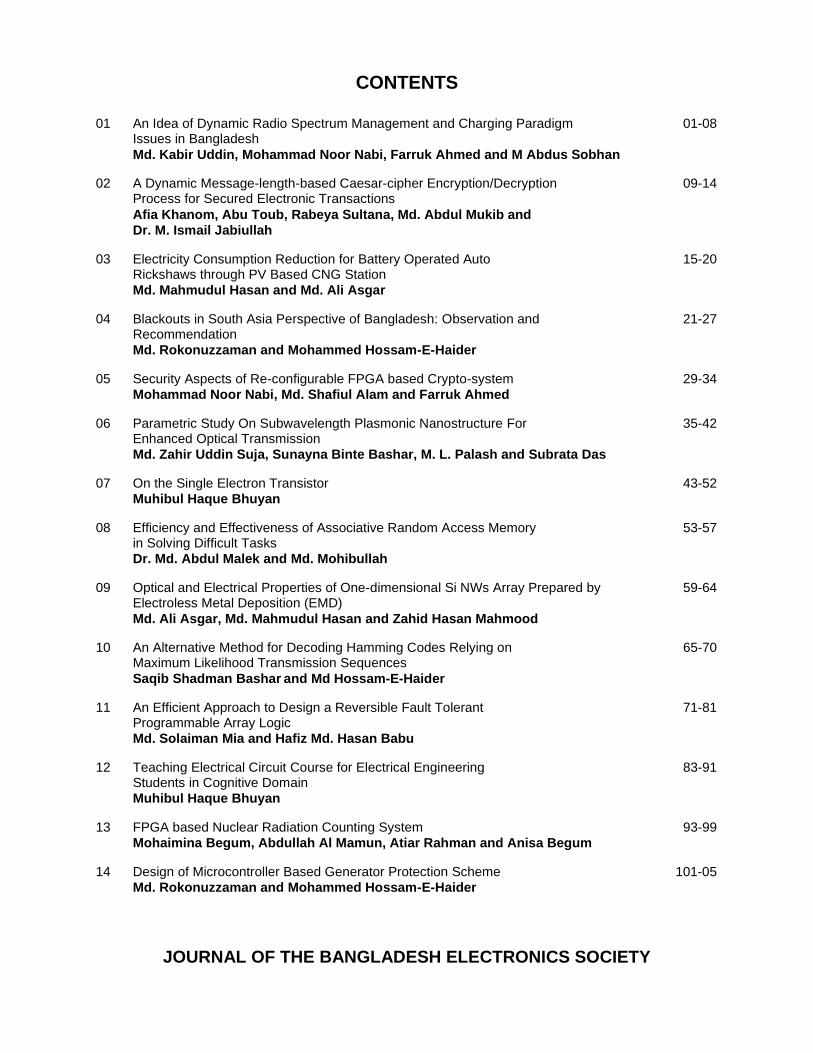
Harmonized Usages Band (HUB) is a contiguous block of spectrum reserved by regulating authority, such as the BTRC, for controlling dynamic access. Multiple parts of the radio spectrum can be allocated as HUB spectrum. The HUB spectrum can be assigned to individual network operators or users to support multiple different services. For example, it can support mobile CDMA and TDMA voice and data services and OFDM fixed wireless services. For a geographical region, allocation of various parts of HUB spectrum to individual networks or users is controlled by the spectrum Broker (Figure 01) [2]. The spectrum broker grants a time bound lease to the requesters for a given amount of spectrum. Key to the operation of this spectrum broker is the pricing and allocating algorithms.
Fig. 1: Spectrum Allocation Model
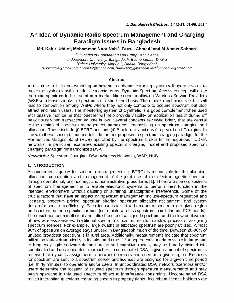
B. System Architecture of Harmonized DSA
The main component of the proposed Dynamic Intelligent Management of Spectrum for Ubiquitous Mobile Network (DIMSUMNet) cellular architecture (Figure 02) are: (i) a Spectrum Information and Management (SPIM) broker (ii) a Radio Access Network (RAN) consisting of new type of base stations (iii) a RAN Manager (RANMAN), and (iv) new intelligent end-user devices. DIMSUNNet employs two new control protocols: (i) Spectrum Lease (SPEL) protocol and (ii) a Spectrum Information Channel (SPIC) protocol between the BS and the end-user device [7]. The SPIC protocol is used to determine the amount of unused spectrum currently available while the SPEL protocol is used in the request and allocation of spectrum.
Fig. 2: Cellular Architecture with Coordinated DSA

3
The spectrum broker is responsible for the pricing and allocation of spectrum and perceives time only in batches or windows of T time units called allocation frames. A pricing paradigm has been proposed in this paper which is combination of dynamic pricing models (i.e. auction and peak-load pricing). Requests received in a time window (n-1), if accepted, are allocated in window (n). The allocation paradigm will processes all of the requests in each frame. Spectrum may be allocated to one or more base station depending upon the original request and available spectrum. The allocation of the spectrum must be consistent with established RF engineering rules. For example, the allowable frequency reuse factors for the reuse of channels must be followed. The complexity of the allocation algorithm will increase when combinations of different technologies are allowed (i.e. CDMA, TDMA, AND OFDM system). The HUB band resembles a licensed band in that the spectrum lease is a short-duration license. This system allows for either the network operator or the individual end-user to request spectrum. It will be only considered requests for spectrum from the network operators. This license could be allocated for a single time period (T) or for multiple periods (stickness) according to the operators’ preferences and the licenses’ demand or availability. In this particular model the auctions may consist of a single round or multiple, allowing the users to bid for single homogeneous licenses or combinations.
The network operators will independently determine their need for spectrum in a given region for the next time period T. A request for spectrum, in increments of the RF channel bandwidth (1.25 MHz), is delivered to the spectrum broker during the auction period. These requests are region specific (i.e. for one or more base stations). A single bid is required for each 1.25MHz RF channel in a single round. For example, if a service provider requires two 1.25 MHz channels, it would issue two bids; one for each RF channel. When all requests are received, the broker determines the ‘winners’ (following a price and allocation algorithm) and spectrum is assigned for a period of T units.
3. SPECTRUM PRICING
A. Auction Pricing
In 2008 the BTRC organized the first spectrum auctions in Bangladesh and it continues to run auction to allocate spectrum based upon the increased demand for wireless networks. BTRC spectrum auctions are open to any eligible company or individual that submits an application and initial (‘upfront’) payment, and is found to be a qualified bidder by the commission [3]. Current spectrum allocations assign licences for a long duration (i.e. 15 years) and over a wide geographic area.
Multiple licences are put in auction in discrete two-stage bidding rounds. The bids are sealed, and are placed per individual license, exceeding the corresponding highest previous bid by a maximum increment (‘activity rule’). A frequently used method of calculating a bid increment is a specific percentage amount (i.e. 10%) of the highest bid. The termination rule is described as one round that consists of no bids. The payment rule follows the ‘pay-your-bid’ pricing. Two types of auctions (i) Simultaneous Multiple-Round (SMR) auctions and (ii) Package bidding (not yet implemented by the BTRC), in the packet bidding bidders may place bids on groups of licenses to encourage straightforward bidding and permits bidders to employ flexible backup strategies. Limitations in this type of auctions include a possible bias to bidders seeking large aggregations due to a variant of the free-rider problem, called the threshold problem, where a single license is part of an entire package that somebody else wants. If all combinations are allowed, identifying the revenue maximizing assignment is an intractable integer programming problem when there are many bidders and licensed. In USA auction Nr. 31 refers to package bidding but is still on hold and the FCC is negotiating to finalize the auction rules with the operators.
Both auctions should plan with long bidding periods and ending with an increase in the number of rounds per day and a decrease of the duration per round. If a bidder is not able to maintain the activity in a given round, it may use an activity rule waiver (if available) or lose its eligibility.

4
Usually each bidder is allowed three waivers. The bidders are able to review the results with a web Brower and the Auction Tracking Tool. The auction ends when there is only one remaining bidder and all bidding actually stops. The winners requested to complete the license down payments after 10 business days.
B. Peak Load Charging
Peak Load Charging (PLC) refers to the pricing of economically nonstorable commodities whose demand varies periodically. PLC is often used by electricity, telephone and other public utilities and also the Internet as a means of reflecting the investment have made to meet peak demand for their services. This pricing scheme corresponds to high competition and price discrimination problems when efficiency in needed due to the increasing role for services in the economy. Therefore it is ideal for industry practice and real world applications. The author will depict the PLC model and how its constraints could be translated into the spectrum pricing problem.
PLC refers to the ‘on-peak’ and ‘off-peak’ time period. On peak usually is described when the demand of the product exceeds the supply and additional units should be produced, when off peak is considered as the condition when supply satisfies the demand. According to the literature the market conditions determine which period is ‘high’ and which season is ‘low’. Usually the model is applied to monopolistic markets where the units’ producer i.e. the regulated sector has full control of the management environment but today is spread over competitive industries i.e. airlines and hostels. The constraints of the PLC after deriving efficient prices are mainly to maximize the welfare profit, called also the net social benefit and optimize the producer’s profit in terms of revenues.
As illustrated in Figure 03 the producer charges a higher price (PHi), PHi =b+β, the b equals the operational cost and β is the cost of providing a unit of additional capacity, during peak times
(DHi) and a lower price (PL0), PL0=b, during off-peak times (DL0).
Fig. 3: PLC Scheme
Building on M. Crew model [8] the following equations derive for the welfare equation:
ω=TR+S-TC (i)
If the total revenue gathered is TR and S is consumers’ surplus, and TC goes towards the total costs, then the difference, ω, is the net social benefit.
ω = x
0P(x) dx-C(x) (ii)
P(x) for demand function, C(x) for total cost function, and X for x1, x2 ... ... xn is the total demand.
In other cases during the peak hour diverse technology might be deployed to help fulfill the demand. For instance during the peak-period it may be more economical to employ an additional technology type to meet the peak-period demand, anticipating lower construction costs and higher operating costs, thus offering cost advantages.
A very interesting case is the PLC with demand and supply uncertainty. “Efficient pricing rules require consideration of willingness to pay for services rendered, when supply is sufficient to

5
meet demand, and for services not rendered plus any rationing cost incurred in excess demand states”. In this case the possibility of “outage” arises, which is the excess demand in certain states. The costs associated with outage are separated into three elements (1) rationing cost, which is the cost incurred by utility in allocated scarce supply (2) disruption cost and (3) surplus loss. Assuming multiple time periods, the price in each time period should be set equal to the expected, deterministic short run marginal cost, including the expected marginal disruption and rationing costs. On the capacity side, per unit cost equals the expected marginal disruption and rationing costs. Summarizing the utility needs to use both price rationing as well as quantity rationing to efficiently allocate available capacity.
According to the PLC theory there are two models under uncertainty mode; the one refers to single technology and single pricing period and the second to multiple periods and multiple technologies. Assume T periods, t=1, ... ...T of equal length in a typical day. Demand in period t is denoted as Xt (Pt, ωt), ω ε Ω and is assumed to be only a function of Pt. P equals to p1,p2, ... pt the vector of T prices. Assuming also several technologies h equals to 1, ... ...,H. The available capacity would be defined as
Zh (Y,ω)=
hS
j
j
1
(Yjω) (iii)
Consequently the Ut, willingness to pay function at period t is
Ut (Q,ω) = Q
0Pt (X, ω) dx (iv)
Pt(X,ω) is the demand function. According to the theory of peak-load pricing there are certain conditions developed to characterize the optimal reliability and capacity, where the formulas are getting more complicated.
In a single pricing period with only one technology used the optimal price could be calculated as following. The optimal price will include also the willingness to pay (Λ). Assuming that the system is characterized with multiplicative uncertainty the optimal price will be the product of maximizing the welfare function for single technology and single pricing period:
P**=b + (
) – Λ ------------(v)
Where b usually is the operating cost at the agent’s side to handle as many operators and bids configured i.e. Internet cost, software updates. β usually is the cost of producing an additional unit, in this case would be the opportunity cost if the licenses were assigned to different operators in that particular time window T; α, γ parameters defined in the theory of peak-load charging [8].
There are several pricing periods but the author assumes the simple case with only one technology CDMA, considering homogeneous networks and licenses. As a result it will be easy to formulate problems with the equations (iii) and (iv) defining the optimal reliability, capacity and optimal price under the condition of h equals to 1. In that case it can be calculated the optimal price in each pricing period, similarly with equation (v).
The PLC is gaining relevance, including the two reasons. “First, with growing competitiveness of the market for interconnection services, the regulator tends to replace the regime of fixed prices with a price-cap regime. Second, since the Internet user is biased towards off-peak times, Internet service providers have an interest in more refined PLC of call-origination charges”.
4. PEAK LOAD SPECTRUM CHARING PARADIGM
Described the two most popular dynamic pricing models it is obvious that the ‘one size fits all’ does not work in this spectrum problem. There are certain pricing models on telecommunications proposed in Pricing Communication Networks, but they could serve more the bandwidth specifications and requirements rather than following the spectrum terminology, where the source is broken into channels and it is not treated as an entity and also there is no congestion factor.
6
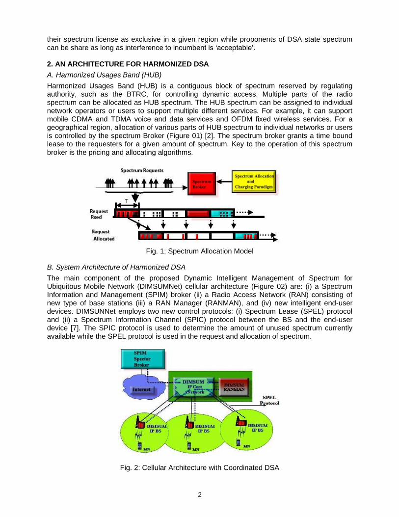
A hybrid dynamic pricing approach can be proposed using the advantages of auctions and PLC. The author argues that during the off-peak time the PLC approach is used, when during the peak-period the auctions mode is more appropriate. In the off-peak time the price is decided from the peak load charging, when in the auction mode, the system is using as reserve the price that was decided in the last off-peak period and was stored in the table of a database. The system is querying the database and is deciding about the auction’s reserve price in Figure 05. The system is managed from an agent described as information broker, is hosting an application that consists of a paradigm that handles the spectrum demand and according to the network load decides what pricing model to apply. Also the agent is aware of the spectrum utilization of each user that owns a chunk of the spectrum. The ultimate goal of the broker is to allocate the spectrum efficiently and assign the winners, determining about the price they have to pay. The capacity is measured as the number of available licenses or channels that could be assigned to the mobile wireless operators that request additional spectrum for each time period T.
Fig. 4: Peak Load Charging Paradigm’s Timeline
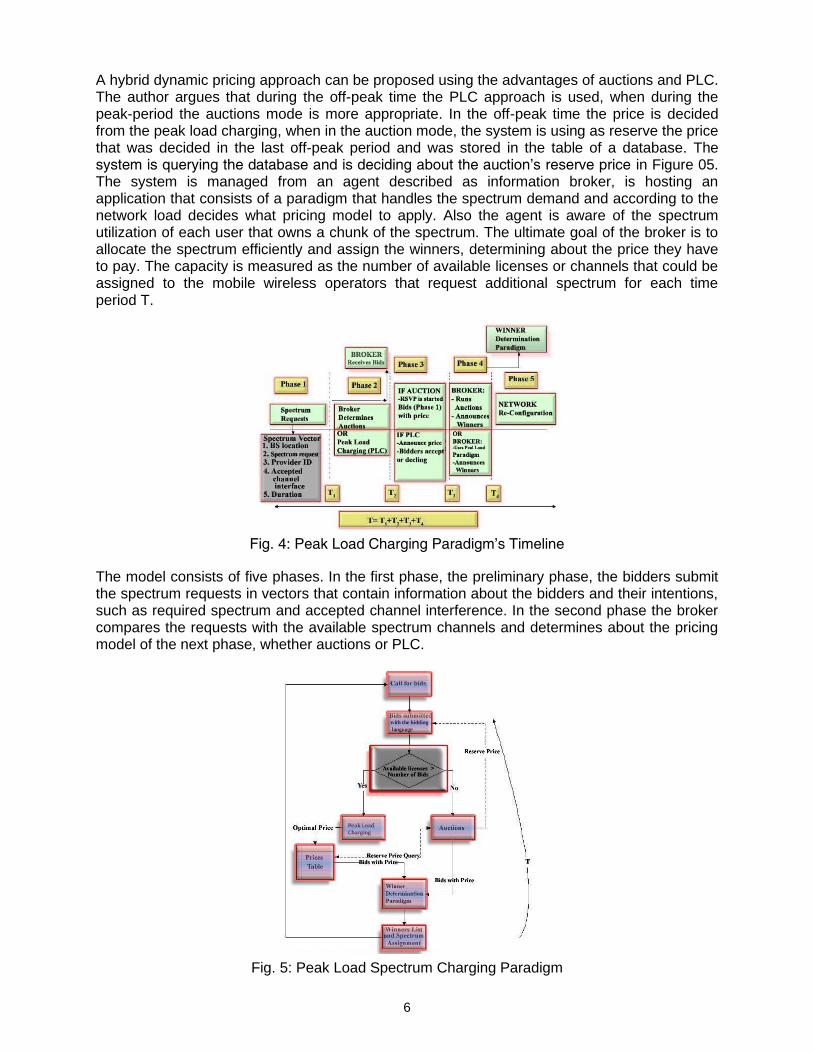
The model consists of five phases. In the first phase, the preliminary phase, the bidders submit the spectrum requests in vectors that contain information about the bidders and their intentions, such as required spectrum and accepted channel interference. In the second phase the broker compares the requests with the available spectrum channels and determines about the pricing model of the next phase, whether auctions or PLC.
Fig. 5: Peak Load Spectrum Charging Paradigm

7
After the broker is making the decision, enter the third phase. In case of auctions the broker is querying the database to determine about the reserve price. Then the bidders complete their vector submission adding the price. In case of PLC the broker computes the price. It is calculated by applying the single technology with multiple pricing periods. The input would be the bid vector as described in phase1 and for each time period T a different optimal price will be calculated and announced to the bidders as the price they have to pay per channel, in order to gain access to additional spectrum. The optimal price after calculated is stored in a simple database or a buffer; each entry into the database’s table is related to a time stamp, in order to keep track of the historical date and the price. At the step T2 the broker receives all the bids and is ready to manipulate them. In phase 4 the broker runs the auction, when for simplicity the author assumes only one round with a single-unit auction without any negotiation included between the broker and the bidders. In order to announce the winners, the brokers run a winner determination algorithm similar to ‘Integer programming for combinatorial auction winner determination and Algorithm for optimal winner determination in combinatorial auctions’. The applied winner determination algorithm ‘weighs’ also other parameters besides the bidders’ price such as ‘Stickiness’, emergency or high priority issues and social welfare. The algorithm should be able to rank the winners according to the previous and announce the winners. Finally in phase 5 the spectrum winners reconfigure their equipment into the new frequency.
There are several advantages of this pricing algorithm. First it is not only based on price to determine about the winners but also other critical parameters. This increases the system’s fairness and efficiency aiming to grant access more often to the ‘small player’ and reveal also the real demand and the bidders’ preferences.
A second advantage is that system is flexible to assign price anytime, computing the optimal price for each time period. The database as introduced in converting the whole application into an efficient system based on historical data enhancing the whole process. The mentioned system is a comparison between a peak-load pricing paradigm and any single-unit paradigm deciding about the optimum solution according to the revenues and the spectrum’s allocation efficiency.
The author identifies the following similarities and differences between the BTRC auctions and mentioned pricing model Table-I. It aims to perform a faster per-auction process, where the licenses’ agenda will be according to the initial bidders’ preferences. The same bid increment formula will be used as suggested in the BTRC auctions, but no waivers will be allowed to let the bidders express their willingness to acquire the license and stay in the game. The bidders could bid in different simultaneous auctions that will include only one stage with a couple of rounds which will be investigated further in the future. The announced list of license should be interference free especially at co-located regions. The broker should be an artificial intelligent agent that will host advanced allocation and pricing algorithms. A web based platform will allow the bidders to participate in auction characterized from efficient spectrum reuse.
Table 1: Comparing Mentioned Pricing Paradigm and the Current BTRC Model
SIMILARITIES DIFFERENCES
Pre-auction process required Faster per-auction process
Bid increment rule No waivers allowed
Combinations allowed Feasible restricted list of combinations allowed due to interference at co-located regions
Winner determination More advanced allocation and pricing algorithms increasing the fairness
Agent with algorithms required Artificial intelligent agent running the process in each time windows T
Simultaneous auctions One-stage
Operator’s infrastructure planning Short term investment
Web based Efficient spectrum reuse
8
5. CONCLUSION AND FUTURE WORKS
This system could have also a practical value, since the applied pricing models are used in real problems and applications. Its practical perspective is increasing the research value and is motivating the researches for further studies. Economic theories have been used to analyse networking and communications problems where interacting decision-makers have conflicting objectives. In particular, auction and game theories are good tools to deal with distributed problems from an economic point of view. This is because the service quality that each user receives in a competitive environment is often affected by the action of other users who also try to contend for the same pool of resources. In a single unit auction, Vickrey proved that ‘English’ and ‘Dutch’ type auctions yield the same expected revenue under the assumptions of risk neutral participants and privately known value drawn from a common distribution [6]. Dynamic Spectrum Allocation coupled with fine granularity switching of services by end-users will engender a flexible and competitive environment for trading wireless services. In this regard, auction and game theories that are captured the interaction among spectrum broker, service providers, and end-users in a multi-provider setting. The BTRC should plan to auction Advanced Wireless Services (AWS) spectrum (the bands are around 1.7GHz to 2100GHz) during the summer of 2016. In addition, it also aims to put rules to auction former TV frequencies around 700 MHz and 450 MHz for mobile data because it can reach farther and penetrate walls better than higher frequencies [4-5]. Bangladesh mobile operators are eyeing with interest these upcoming radio spectrum auctions that will open up large amounts of frequencies to mobile data services.
REFERENCES
[1] “Liberalizing US spectrum allocation”, TW Hazlett Telecommunications Policy, vol. 27, no. 7, pp. 485-499, Aug. 2003
[2] T. Kamakaris, M. Buddhikot, R. Iyer, “A Case for Coordinated Dynamic Spectrum Access in Cellular Network”, Proceedings of 1
st IEEE DySPAN, Baltimore, MD, Nov. 2005
[3] Bangladesh Telecommunication Regulatory Commission (BRTC): www.brtc.gov.bd
[4] Md. Kabir Uddin and M Abdus Sobhan, “
On the Implications of Current Radio Spectrum Management Issues in Bangladesh.”, IJCSIS, Vol-12, No- 3, page 16-21, 2014
[5] Md. Kabir Uddin, “A Comparative Study of Radio Spectrum Pricing for 3G and WiMAX in Asia and Europe Countries”, MSc in ETE Thesis, IUB
[6] Vickrey W.S., and Bell, “Responsive Pricing of Public Utility Services”, Journal of Regulatory Economics, vol. 2, no.1 pp. 337-346, Spring 1971
[7] Mr. Kabir Uddin, and Md. Abdur Rouf Khan “Network Wide Statistics of TCP Indicators Measurement Reassume the Status of the 3G Network Monitoring”, UITS, 2015
[8] M. Crew, C. Fernando, and P. Kleindorfer, “The theory of peak-load pricing: A survey”, Journal of Regulatory Economics, vol. 8, no.3, pp.215-248, Nov.1995
9
J. Bangladesh Electron. 14 (1-2); 09-14, 2014
A Dynamic Message-length-based Caesar-cipher
Encryption/Decryption Process for Secured
Electronic Transactions
Afia Khanom, Abu Toub, Rabeya Sultana, Md. Abdul Mukib and Dr. M. Ismail Jabiullah
Department of Computer Science and Engineering, Hamdard University Bangladesh E-mail: [email protected]
Abstract
A message-length-based Caesar cipher generation technique has been designed, developed and implemented for secure communication of the electronic documents. The encryption/decryption key is found by calculating the number of plaintext that is to be transmitted through the electronic transactions. In this paper, an improved Caesar cipher generation technique based on symmetric key encryption algorithm has been proposed that uses ASCII values of input text as the encryption process and length of text message to encrypt the text data. First, take a message as character that is to be sent to the destination and counts the length of the message. Then these characters convert in equivalent ASCII code. It adds length of message and the ASCII code. Convert this value in binary number in nine bit and save it in data file. This data file called file of cipher text and this process is called encryption. This produced data in this process is called cipher text and is to be sent to the destination for the recipient. In the receiving end, the reverse process is performed for retrieving the plaintext of the message. Here, message-length is dynamically changeable and establishes better security than that of the conventional Caesar cipher process. It can be applied in any practical cryptographic process or lab works.
1. INTRODUCTION
Secured Electronic transactions are very much desirable in this age of Internet and web based transactions. The security depends on the message is being communicated and the attacks between the communicants of the transactions. To satisfy the needs of the secured electronic transactions, the communicating parties must communicate to each other through the Internet in a strong secured cryptographic process. The way to make special messages security in the electronic communication system, message encryption/decryption process has introduced. Message encryption/decryption is the technique which performs some cryptographic operations on the intended message and makes an encrypted message. This encrypted message is then transmitted to the recipient through an unsecured way. Those who have no idea about the operations performed in encryption/decryption can never understand the encrypted message. The receiver then performs another predefined operation on the encrypted message and gets the real message. The real message is known as plaintext, the encrypted message is known as ciphertext and the overall process is known as cryptography. There are several ways of cryptographic communication systems. One of the most popular communication medium is messaging enciphering where message is encrypted in the sender side by using a symmetric encryption and a shared secret key, then the output is sent to the destination and in the receiver side, the received message is decrypted by using the same secret key and the decryption algorithm to retrieve the original message. The transmitted message is remained secured in the communication path to other parties since they do not know the encryption/decryption method and the shared encrypted/decrypted key. The party other than the intended communicants knows only the ciphertext and that is why they do not retrieve the original message from the ciphertext without using the exact key. For secure communication, it is trying to make a more complex encryption/decryption algorithm and a stronger shared secret key to use in the

10
electronic transactions. There are two basic types of operations used in cryptography, one is substitution and another one is transposition. A substitution cipher is a method of encryption by which characters of plaintext are replaced with ciphertext according to a regular system. The receiver deciphers the text by performing an inverse substitution. There are some encryption techniques which can be easily breakable to retrieve the plaintext, they are not reliable to use but many of them are more reliable to use. The security of the encrypted message depends on the strength of the encryption operation. So, the operations performed to encrypt a message should be so powerful that it cannot be broken easily. Caesar cipher is one the well-known cipher generation technique in the cryptography and is introduced here for establishing a secured electronic message communication system with dynamic session keys. An unauthorized person may want to decrypt the ciphertext to retrieve the actual message. For this, the encryption/decryption key generation mechanism is used from the message length in the cipher generation technique and the transaction process establishes a more secured and stronger electronic message communication system.
2. CONVENTIONAL APPROACH
A substitution technique is one of the cryptographic process in the letters of the plaintext message are replaced by other letters or by numbers or symbols of the alphabets of the ciphers. This technique involves replacing each letter of the alphabet with the letter standing the number of the of the message length further down the alphabet in round cases. The alphabet is wrapped around. Here, a numerical equivalent value of the letter is assigned and is calculating the ASCII value for performing the cipher generation. The algorithm can be expressed as by the following equation. For cipher generation from the plaintext, the process is:
C = E(p), where E(p) = (p + key) mod (number of the alphabet)
For plaintext generation from the cipher text, the process is:
p = D(C), where D(C) = (C - key) mod (number of the alphabet)
This is known as the ciphertext of the Caesar cipher, then the brute-force cryptanalysis is easily performed that is, simply try all the possible keys of the number of the encryption key. Three important characteristics of the of this process enabled the users to use the brute-force cryptanalysis and they are:
The encryption and decryption algorithms are known.
There are only the keys of the number of alphabets to try.
The language of the plaintext is known and easily recognizable.
In most networking situations, one can assume that the encryption/decryption algorithms are known. Generally, the brute-force cryptanalysis for this cipher generation is impractical to use the algorithm that employs a large number of keys. The third characteristic is also significant and may be usable. There are more approaches to do the encryption/decryption by using this cipher generation by using the dynamic keys that are generated from the plaintext that are to be transmitted in the communication.
3. PROPOSED METHOD
The proposed method of encryption/decryption is basically based on the calculation of the intended message length and that is used as the key for encryption and decryption. The encryption process, algorithm of the encryption process, decryption and the algorithm of the decryption process is depicted in the below.
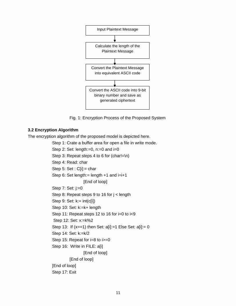
3.1 Encryption Process: First, take a message as character that is to be sent to the destination and counts the length of the message. Then these characters convert in equivalent ASCII code. It adds length of message and the ASCII code. Convert this value in binary number in nine bit and save it in data file. This data file called file of cipher text and this process is called encryption. This produced data in this process is called cipher text and is to be sent to the destination for the recipient. The process is depicted below.
11
3.2 Encryption Algorithm
The encryption algorithm of the proposed model is depicted here.
Step 1: Crate a buffer area for open a file in write mode.
Step 2: Set: length:=0, n:=0 and i=0
Step 3: Repeat steps 4 to 6 for (char!=\n)
Step 4: Read: char
Step 5: Set : C[i]:= char
Step 6: Set length:= length +1 and i=i+1
[End of loop]
Step 7: Set: j:=0
Step 8: Repeat steps 9 to 16 for j < length
Step 9: Set: k:= int(c[i])
Step 10: Set: k:=k+ length
Step 11: Repeat steps 12 to 16 for i=0 to i<9
Step 12: Set: x:=k%2
Step 13: If (x==1) then Set: a[i]:=1 Else Set: a[i]:= 0
Step 14: Set: k:=k/2
Step 15: Repeat for i=8 to i>=0
Step 16: Write in FILE: a[i]
[End of loop]
[End of loop]
[End of loop]
Step 17: Exit
Input Plaintext Message
Calculate the length of the
Plaintext Message
Convert the Plaintext Message
into equivalent ASCII code
Convert the ASCII code into 9-bit
binary number and save as
generated ciphertext
Fig. 1: Encryption Process of the Proposed System

12
3.3 Decryption Process: In another part of the proposed model for receiver to read the data file as character and count the length of message. Divide the length by nine to find the number of character of real message. Take nine binary numbers and convert it in integer. Omit the number of characters from the converted integer value which is an ASCII code. Then convert ASCII code into character. By this process convert all binary numbers in character and show them in text message.
3.4 Decryption Algorithm
The decryption algorithm of the proposed model is presented below.
Setp1: Crate a buffer area for open a file in read mode.
Step 2: Set: i:=0
Step 3: Repeat step 4 to 15 for (g!=\n)
Step 4: Read: char
Step 5: If c=0 then Set: a[i]:=1 Else Set: a[i]:=0
Step 6: Set: i=i+1
Step 7: Set: length: =i/9
Step 8: Repeat step 9 for L=0 to L<i
Step 9: Set: h=0
Step 10: Repeat steps 11 to 14 for j=L and k=8 to j<=L+8
Step 11: Set: a[j]=a[j]*2k
Step 12: Set h=h+ a[j]
[End of loop]
Step 13: Set: h:=h-length
Step 14: g=(char)h
Step 15: Write: g
[End of loop]
Step 16: Set: L=L+9
[End of loop]
Step 17: Exit
4. IMPLEMENTATION
The proposed model is implemented by using the C++ programming language for analyzing its clarity, simplicity, and the security of the process. It is tested and verified for several input messages and found better security than that of the conventional system. For example, if one input any text message in the running program, than he/she can easily realized its activity. The some implemented input/outputs are presented below.
Input: Sender Site Encryption
Enter text=My name is afia khanom suny. I am a sutdent of CSE of HUB. I am a student of 1st batch. My id is 315122004.
Generated Key: 107
Process returned 0 (0x0) execution time: 151.905 s
Press any key to continue.
Cipher text:
01011100001110010001000101101101100101100110001101100001101000001000101101101010001101111001000101101100110001101000101101010001100110001000101101101011
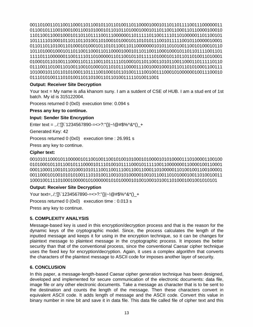
13
0011010011011001100011011001011011010011011000010001011011011110011100000011011001011100100010011001010001011010110100010001011011001100011011000010001011011001100010001011011011110011100000011011111011001111011010000011011001011011111010001011011011010011010001010001011010101110010111110010110000010001011011011010011010001010001011010110011011000000010101101010011001010001011010110100010001011011001100011011000010001011011001100010001011011011110011011111011100000011001111011010000011011001011011111010001011011011010011010001010001011010011100011011110011011111010001011011001101011001100011011111011001110011010011010011001010001011010111000011100100010001011011010100011001111010001011011010100011011110010001011010011110010011100010100000010011100010011101010011101010011011010011011010011111010011001
Output: Receiver Site Decryption
Your text = My name is afia khanom suny. I am a sutdent of CSE of HUB. I am a stud ent of 1st batch. My id is 315122004.
Process returned 0 (0x0) execution time: 0.094 s
Press any key to continue.
Input: Sender Site Encryption
Enter text = ,./;'[]\`1234567890-=<>?:"{}|~!@#$%^&*()_+
Generated Key: 42
Process returned 0 (0x0) execution time : 26.991 s
Press any key to continue.
Cipher text:
001010110001011000001011001001100101001010001010000101010000111010000110010001010001011011001011100001011101001011110001011111001100000001100001001100010001100011001011010001010111001100111001100110001101000001101001001100100001001100010100101010100111010100110010101000001001011001101010001001101001001110001001111010001000001010000001010100001010010001010011010001001001010101
Output: Receiver Site Decryption
Your text=,./;'[]\`1234567890-=<>?:"{}|~!@#$%^&*()_+
Process returned 0 (0x0) execution time : 0.013 s
Press any key to continue.
5. COMPLEXITY ANALYSIS
Message-based key is used in this encryption/decryption process and that is the reason for the dynamic keys of the cryptographic model. Since, the process calculates the length of the inputted message and keeps it for using in the encryption technique, so it can be changes for plaintext message to plaintext message in the cryptographic process. It imposes the better security than that of the conventional process, since the conventional Caesar cipher technique uses the fixed key for encryption/decryption. Again, it uses a complex algorithm that converts the characters of the plaintext message to ASCII code for imposes another layer of security.
6. CONCLUSION
In this paper, a message-length-based Caesar cipher generation technique has been designed, developed and implemented for secure communication of the electronic documents: data file, image file or any other electronic documents. Take a message as character that is to be sent to the destination and counts the length of the message. Then these characters convert in equivalent ASCII code. It adds length of message and the ASCII code. Convert this value in binary number in nine bit and save it in data file. This data file called file of cipher text and this

14
process is called encryption. This produced data in this process is called cipher text and is to be sent to the destination for the recipient. The encryption/decryption key is found by calculating the number of plaintext that is to be transmitted through the electronic transactions. This is an improved Caesar cipher generation technique based on symmetric key encryption algorithm that uses ASCII values of input text as the encryption process and length of text message to encrypt the text data. Here, message-length is dynamically changeable and establishes better security than that of the conventional Caesar cipher process. This process has been implemented for several input messages and analyzed the outputs of the designed programs. This cryptographic technique can be applied in any practical cryptographic process or lab works.
REFERENCES
[1] Hamid Mirvaziri, Kasmiran Jumari Mahamod Ismail and Zurina Mohd Hanapi, “Message Based Random Variable Length Key Encryption Algorithm”, Journal of Computer Science 5 (8): 573-578, 2009
[2] William Stallings, Cryptography and Network Security Principles and Practices, 4th Edition ISBN:
0131873164.
[3] William Stallings, Data and Computer Communications, 7th Edition.
[4] Data Communications and Networking, 4th Edition, Behruz A Forouzan.
[5] Encyclopedia of cryptography and security, Henk C. A. van Tilborg.
[6] http://www.asciitable.com.
[7] Udepal Singh, Upasna Garg, “An ASCII value based text data encryption System,International Journal of Scientific and Research Publications”, Volume 3, Issue 11, November 2013
[8] Suyash Verma, Rajnish Choubey, Roopali Soni,” Design and Implementation of New Encryption algorithm Based on Block Cipher Substitution Technique ( Effect on Image file) International Journal of Computer Technology and Electronics Communication” ISSN 2320 – 0081
[9] Majdi Al-qdah & Lin Yi Hui, “Simple Encryption/Decryption Application, International Journal of Computer Science and Security”, Volume (1) : Issue (1)
[10] M. Ismail Jabiullah, Md. Zakaria Sarker, Anisur Rahman and M. Lutfar Rahman, “A secured message transaction approach by dynamic hill cipher generation and message digest concatenation, Daffodil International University Journal of Science and Technology”, volume 5, issue 1, January 2010.
[11] http://en.wikipedia.org/wiki/Numeral_system.
[12] Handbook of Applied Cryptography, Alfred J. Menezes, Paul C. van Oorschot, Scott A. Vanstone.

15
J. Bangladesh Electron. 14 (1-2); 15-20, 2014
Electricity Consumption Reduction for Battery Operated Auto
Rickshaws through PV Based CNG Station
Md. Mahmudul Hasan1 and Md. Ali Asgar2
Department of Electronics and Communication Engineering, Jatiya Kabi Kazi Nazrul Islam University, Trishal, Mymensingh, Bangladesh
Abstract
People all over the world have keen interest to look for a new way for leading a comfortable life. Accordingly various technologies have been invented in transport system. Battery operated Auto-rickshaws are a motorized version of the traditional pulled rickshaw. It is found that Bangladesh is now overwhelmed with battery operated auto-rickshaws and it is an essential form of urban transport. In this paper, as a transport mode, an analysis in using battery operated auto-rickshaw is studied pragmatically and an illustration is provided technically and financially. Results show that the battery-run auto-rickshaw has been consuming a substantial amount of electricity daily from the national grid. An effective way of using PV based CNG station has been given to reduce consumed power from our national grid by a comparative analysis through this paper.
Keywords: Battery operated auto-rickshaw, Electricity, Auto-rickshaw, CNG Station, Urban transport, Solar PV Systems
1. INTRODUCTION
Bangladesh is an over populated country with more than 160 million people. With this number of people economic activities are increasing day by day. With more economic activities more power demand is growing promptly all over the country.
Power crisis is the main problem now a day all over the world and hence people are trying to improve the technologies in various sectors to mitigate power crisis. Transport sector is one of the issues now a day consuming a lot of energy from natural oils. For this reason, scientists are always trying to develop new technologies to mitigate burden on natural energy sources and to rely on renewable energy sources.
Battery operated auto-rickshaw (locally called 'Easy-bike') is a newly added transport mode in urban transportation system of Bangladesh. It gains much popularity among urban passengers since it involves lower travel cost than other locally available transport modes as well as provides reasonable safety and comfort to the users during travel [1]. This popularity, in turn results rapid growth of the mode in urban areas of Bangladesh. Now, the mode has become inseparable part of urban peoples’ mobility network, especially in small-compact towns [2]. Therefore, it requires careful attention to incorporate this mode in local urban transport system.
Electricity demand in Bangladesh is increasing fast due to enhanced economic activities. The total generation capacity in Bangladesh was about 8100MW in the fiscal year 2011-2012 and the maximum peak generation was approximately 6066MW in the same fiscal year and the maximum demand in this fiscal year was nearly 7518MW [3]. Under the existing generation of electricity in Bangladesh, renewable energy has a very small share of about 0.5% to the total generation. Bangladesh Power Development Board (BPDB) has set policy for developing renewable energy resources to meet 5% of the total power demand by 2015 and 10% percent by 2020[4].
This paper offers an innovative idea to mitigate the electricity consumption for Battery Operated Auto-rickshaw or commonly know as easy-bike through detailed mathematical analysis,

16
discussion on technical issue, energy demand and financial factors. It also proposes a solar based recharging station for mitigating burden on national grid.
2. BACKGROUND STUDY OF AUTO-RICKSHAW
Auto rickshaws are a common means of public transportation in many countries around the world. Mainly two types of auto rickshaws, CNG run auto rickshaw and motor driven auto rickshaw or easy bike is plying on the roads in Bangladesh. The easy-bikes look somewhat like CNG-run auto-rickshaw and run by a motor set under the body and are powered by five rechargeable batteries which are set under the seat (Fig.1). Commercially available easy bikes have flooded the country, consuming a substantial amount of electricity daily from the national grid. Each of the auto-bikes which has to be charged eight hours daily, consumes 7-8 units of electricity per day [5]. This additional huge consumption of energy by electric vehicle is a burden to the national grid.
Fig.1: Battery run auto rickshaw
3. USUAL ELECTRICITY CONSUMPTION AND COST
Technology is being improved day by day in the world. Developing countries are not also behind in this race.
A small motor is attached under the body of the rickshaw. Since it runs with a battery bank, a low cost electric charger is used to charge up the battery bank anywhere and all types of battery run electric vehicles can be considered as a non-polluting transport system in this regard.
The battery run auto-rickshaw is an integrated system with motor, controller, battery and charge controller. The cost of a single easy bike system is around BDT. 120000-135000. Above 5, 00,000 easy bikes are plying on the roads all over the country.
Daily energy consumption, as obtained from the BPDB data, by a single easy bike is 7-8unit/day and 240unit/month. It is 120,000,000kWh per month for 500000 easy bikes. So, the total cost of energy consumption using grid supply is about BDT. 720,000,000/month and BDT 8640,000,000/year in commercial sector.
4. DESIGN Of RECHARGING STATION
The long term commercialization of utility based solar Photovoltaic (PV) electric generation requires the development of safe, efficient, reliable, affordable components and systems that meet utility expectations of performance and production goals, while allowing for full integration of time variant intermittent renewable generation resources.
In Bangladesh, Solar panel inclination angle varies from place to place to obtain optimum energy output from the panels. The energy harnessing efficiency of the solar panel is

17
considered 90% at this setting. Depth of discharge (DOD) of the battery is 85%. In this system, high module temperature, dust settlement on PV modules and other factors that degrade the solar cell performance would decrease the amount of capacity (Ah) produced by the PV modules.
4.1 Design of a solar based recharging station
A standalone PV system is simple because the output from a PV module is always DC. Standalone systems vary widely in size and application. A charge controller may be incorporated in the system to avoid hazardous of battery damage by excessive charging or discharging and optimizing the production of the cells or modules by Maximum Power Point Tracking (MPPT).
The easy bike is driven by 3kWh of battery bank and a system voltage of 60V. Average bright sunshine hour is considered as about 5 hours in Bangladesh. The PV panel need to supply the energy to the battery bank at 60V. Therefore total capacity (Ah) generated by the PV panels should be 3000Wh/60V = 50Ah. So PV modules should produce the following amount current for a single easy bike.
At system voltage 60V
In this work, Selected PV module has max power at STC is 170W [6] which at maximum power point (Vm and Im) would be about 34.8V and 4.9A respectively. So for this system, it is required
and 2 modules in series to get voltage higher than 60V. Thus overall it requires (3 x 2) = 6 PV modules of 170Wp for a single easy bike. But solar based recharging station is designed for charging 10 easy bikes simultaneously. So total PV module is (6 x 10) = 60 Nos. Therefore, the solar based recharging station will be 10200Wp system.
A system capacity design depends on the amount of space. A rule of thumb is that a square foot of single PV module area produces 10 watts of power in bright sunlight [7]. After site selection, stations can add more numbers of easy bikes multiplying the easy bike with a system capacity. The solar based recharging station can charge easy bike quickly and more easy bikes each day, if battery charge controller with intelligent and improved technology is available in market.
4.1.1 Required total system capacity
Total 5, 00,000 easy bikes are running on the roads in bangladesh. In this calculation, 10,000 of total easy bikes are considered. So, total capacity of battery is 30,000kWh at 60V. Average global solar radiation is 4.55KWH/m2/day. No need to consider autonomous days for system.
Daily Energy demand = 30,000 KWh
Solar Panel harness efficiency = 90%
Battery efficiency = 85%
The Required system capacity = Pp
Harnessed Power will be directly brought up into easy bikes.
Therefore total system capacity should be

18
4.1.2 Tentative spaces for station
The roof of refueling station is the suitable and plenteous place for harvesting solar energy. There is enough space to mount the PV modules on the roof. There are many fuels and CNG refueling stations all over the country. The amount of roof area is needed to mount a system is based on the size or generating capacity or rating of the system. The commercial places can be used for mounting PV modules with a flat consumption of 1.5 W/ft2 [8]. The proposed system is needed 500 square foot space to setup solar based recharging station.
Fig. 5: Tentative Place on the roof of genaral refuel station
After investigation, it is seen that some refueling stations are situated in potential place (Fig.5) where PV system can produce energy without any obstacle and design of panel installation on the roadside (Fig.6) will increase beautiful of town. Some places are not suitable to accommodate PV modules. While designing the solar PV systems, we would be carefully planning the solar array layout to avoid possible shadow from trees, hills, the water tanks, sidewalls, columns and nearby buildings.
Fig. 6:Tentative Place for Panel Setup on the roadside
5. FINANCIAL ANALYSIS OF THE PROJECT
Since motor run auto-rickshaw is integrated with battery and other components, there is no need to use extra battery. The required equipments are PV modules, charge controllers, mountings and other accessories. The different essential components associated with this project are given in Table I with respective quantities and costs for the period of 20 years. In this project the quantities of PV modules and dc combiner boxes are calculated manually. The wiring, installation and maintenance cost is considered approximately. The cost of these components may be varied depending on its brand, quality, place and quantity.

19
Table 1: Cost of the Solar based recharging station
Equipment Unit Cost
(BDT)
Quantity Total Cost
(BDT)
Solar Panel 120/Watt 60 12,24,000
Charge Controller ( DC/DC, 5A-20A, 60V) 500 6 3,000
Junction and Combiner Box for Solar Panel 350 6 2,100
Solar Support Structures 2000 1 2,000
Cable and connectors 1500 1 1,500
Breaker, protection and Others 1000 1 1,000
Transportation, installation, LC and O& M cost (25% of total equipment cost)
- - 3,06,000
Total Cost of Equipment 15,39,600
The total system capacity for the above number of auto-rickshaws required is about 8.618MW. So, about 844 solar based recharging stations are required based on the minimum calculated system in this work. The numbers of recharging stations may vary according to the PV system, based on the space or generating capacity or rating of the system. So, total cost is BDT 129,94,22,400 for solar based recharging station for the period of 20 years.
6. SAVING OF ELECTRICITY CONSUMPTION AND COST
In fine, it has been revealed that the solar based recharging station helps to saving electric energy consumption up to 29200MWh per year. Economic analysis depicts the detail cost of electric energy with BDT 13,14,00,000 per year in commercial sector (BDT4.5/unit). And this much energy avails to meet energy demand in our poor country alongside to reduce load shedding. Even authority can distribute at nearby commercial or residential areas.. Since solar PV systems is for the period of next 20 years, authority can make profit by selling KWh solar energy from solar based recharging station after payback period. The bill cost of easy bikes for 20 years span is around BDT 262,80,00,000 for 29200MWh without analysis of Life Cycle Cost (inflation and degradation). The total cost of 8.618MW solar PV system for period of next 20 years is around BDT 129,94,22,400.
7. CONCLUSION
A Country like Bangladesh where low wages and surplus labor are substantial features of the economy, auto-rickshaws may be the main vehicle for short-distance movement of people and goods. The motor driven auto-rickshaws are environment friendly, carbon emission free, and hence these are being popular all over the country now-a-days. The government of Bangladesh is very concerned about PV system and has taken initiative to distribute PV system throughout the country by various means. Hence the proposed idea can be a reward to minimize the electricity consumption for this number of easy bikes and thus makes life comfortable. So the concerned authority should take the adequate steps for imposing the proposed solar system on the roof of each refueling station as an alternative power source for easy bikes. This proposed system will meet the energy demand for easy bikes as well as reduce the carbon emission from fossil fuels. The generated energy from the recharging stations can be sold per KWh in commercial sectors after meeting the demand of auto-rickshaws. In case authority bans the easy bikes, stations would be used charging battery for SHS and IPS systems.

20
REFERENCES
[1] The Daily Star, “Electric Rickshaws Run out of Steam”, Published on May 30, 2011
[2] The New Age, “Unregistered Easy-bikes Still Plying City Streets”, Published on January 06, 2011
[3] Annual Report 2011-2012, Bangladesh Power Development Board 2013
[4] Renewable Energy Policy of Bangladesh, Bangladesh Power Development Board 2008
[5] Minhaj Uddin, Unauthorised battery-run vehicles flood Chittagong city, The Daily Star news article (December 30, 2012)
[6] [http://www.infinigi.com/sharp-ne170u1-170-watt-solar-module-p-1538.html
[7] [Md. Nawrose Fatemi, Solar ready roof design for high-performaning solar installation in Dhaka: Potential and strategies, ICDRET 2012 P.235 2012
[8] A. Hasib Chowdhury, Nahid-Al-Masood, Manjurul Alam Fuad, Md. Asad Uz Zaman, and Ridwanur Rahman, Savings of Electricity Consumption Cost in Commercial Sector of Bangladesh, International Journal of Innovation, Management and Technology, Vol. 4, No. 4, August 2013

21
J. Bangladesh Electron. 14 (1-2); 21-27, 2014
Blackouts in South Asia Perspective of Bangladesh:
Observation and Recommendation
Md. Rokonuzzaman1 and Mohammed Hossam-E-Haider2
Electrical, Electronic and Communication Engineering Department Military Institute of Science and Technology, Dhaka, Bangladesh
[email protected] and [email protected]
2
Abstract
Though Bangladesh is considered one of the most energy-poor nations, with one of the lowest per capita electricity consumption rates in the world and has tried to improve its energy situation, extending access to electricity to about 3.45 million more people since 2008. But the increasing gap between the demand and supply of electricity has been a matter for concern. The oldest transmission lines system and conventional power skeleton which is one of the most important issues for that causing blackout. Since the power system is a non linear system and changes its operation continuously for that it is very challenging and uneconomical to make the whole system be stable and keep disturbances free. This instability causes large scale blackouts. The Russian experience to facing blackout is one of the proven and comprehensively field-testes, giving concentration on their recommendation this paper is representing a lists of good collection of wide spread power system blackouts that happened in the beginning from 21st century in south Asian territory including authors recommendation perspective of Bangladesh.
Keywords: Blackout, power outage, cascaded failures, grid failures.
1. INTRODUCTION
01 November 2014, Bangladesh is faced the longest power outage, in the morning and in the afternoon, causing a serious disruption of activities all over. After daylong efforts, power was restored to some areas in the afternoon, but at 4:15pm the power supply closed down again. The national grid had failed. The capital city remained in dark till midnight. This unprecedented power cut was the longest in memory.
Last year, from 01 October 2013, Bangladesh began importing electricity from India through a 400-kilovolt transmission line that runs from Baharampur in the Indian state of West Bengal to the southwestern Bangladesh town of Bheramara, Kushtia [1]. A technical glitch at the Bangladesh-India power transmission system in Bheramara, Kushtia are responsible for the blackouts. At the time 438MW of power was coming from India. The glitch put the entire transmission
system at risk and that power supply was shut down. With 438MW of electricity cut from the national grid, a lower-frequency vacuum was created, leading to all the power plants in the country to shut down [2]. Fig. 1 Show the geographical location of Baharampur and Kushtia.
Blackouts can result from many causes. Most large blackouts begin with natural disturbances, or due to the loss of generating units, breaker failures, common tower and common right-of way circuit outages etc. Most of professionals and researcher guessed that the digesting blackouts cause for cascading failures since all the power plants are connected in cascade to the National grids. Fig. 2 Show the satellite view of whole country map during the outage of power grids in Bangladesh.

22
Fig. 1: Baharampur, India and Bheramara, Khustia, Bangladesh in Map.
Cascading failures are one of the main reasons for large scale blackouts in power transmission grids. Large scale cascades are typically due to propagation of a local failure into the global network.
Fig. 2: Blackouts in Bangladesh, 01 November 2014.
This Paper has presented the cascading failures and different observations, recommendations are made which can be able to reduce Blackouts very efficiently and also be a good solution for which affected different power grids in future.
2. CASCADING FAILURES
Cascading failures were traditionally considered as low-probability high-consequence events. Recent cascading failures in several power systems world-wide require an urgent and thorough attention. Adequate analysis, research and development efforts are needed to investigate the cascading processes, determine conditions and triggering events that could cause blackouts, evaluate the consequences and identify potential blackouts, and to develop preventive transmission planning solutions, operating procedures and automatic protection systems.
Blackout prevention is a key task in developing the future power grids. The most common questions that arise in connection to the blackouts in Bangladesh are very similar as follow [3]:
Whether the existing grids are finally pushed to an edge where blackouts are unavoidable and only massive investments into the grid infrastructure and radical restructuring could help to build blackout-free future grids?
Does the existing grid control support an adequate level of grid reliability?
The answer is ‘NO’, based on experience with the blackout prevention systems developed in Russia. While building the future power grids, it is obviously useful to analyze the know-how worldwide.

23
3. ANALYSIS OF RECENT BLACKOUTS
We are analyzing here very nearest to date, some blackouts. Two severe power blackouts affected most of northern and eastern India on 30 and 31 July, 2012. The 30 July, 2012 India blackout affected over 300 million people and was the then-
Largest power outage in history, counting number of people affected, beating the January 2001 India blackout. The 31 July 2012 India blackout was the mentionable one and destructive outage in history. The outage affected over 620 million people, about 9% of the world population, or half of India’s population, spread across 22 states in Northern, Eastern and Northeast India. An estimated 32GW of generating capacity was taken offline in the outage. Electric service was restored in the affected locations between 31 July and 01 August 2012.
A. Blackouts in Bangladesh:
16 November, 2007.
On November 16, 2007, Cyclone Sidr struck the south-west coast of Bangladesh. The blackout was the country's worst knocked out the national grid for 24 hours after the cyclonic storm Sidr had ravaged the coastal areas and again exposed inefficient and dated infrastructure that has held back development in the South Asian nation [5].
15 December 2007.
On December 15, 2007, as supply from the Ghorashal power station tripped, the country was blackouts for four hours [5].
01 November, 2014.
November 01, 2014 blackout in Bangladesh was the largest outage of power in entire history. An unusual power outage has taken over the entire country as the national grid collapsed two times since 11:30am on Saturday. Power supply was being restored partially across the country from 2:50pm. However, the national grid collapsed again at 4:30pm. The outage was triggered by excessive electricity supply from India. The High Voltage DC substation at Bheramara in Kushtia shut down due to technical glitch in the morning. The blackout hit around noon and covered all parts of the country connected to the national grid as other power stations near it started closing down one after another [6].
B. Blackouts in India:
02 January, 2001.
Beginning of the 21st century, first major blackout of the northern grid took place on 02 January 2001, when an estimated 230 million people were affected for 16 hours. Poor and inadequate transmission equipment was blamed for the failure in 2001.The frequencies at which northern grid typically operates is between 48.5Hz and 50.2Hz. At the time of the grid's collapse, the frequency was 50.46Hz, which could have caused or contributed to the failure [7].
30 July, 2012.
At 2:35am local time when the northern grid failed catastrophically somewhere nears the city of Agra, circuit breakers on the 400kV Bina–Gwalior line tripped. As this line fed into the Agra–Bareilly transmission section, breakers at the station also tripped, and power failures cascaded through the grid. All major power stations were shut down in the affected states, causing an estimated shortage of 32GW. It took 15 hours to restore 80% of service.
31 July, 2012.
A faulty relay near to the Taj Mahal, infect power stations across the affected parts of India and maximum area of country again went offline. National thermal power corporation (NTPC) Ltd. stopped 38% of its generation capacity. Over 600 million people (nearly half of India's population), in 22 out of 28 states in India, were without power. As of 02 August, Uttar Pradesh was being supplied about 7GW Power, while the demand was between 9GW and 9.7GW [8].

24
C. ANALYSIS AND RECOMMENDATIONS [9]:
An investigation committee consisted of S. C. Srivastava, A. Velayutham and A. S. Bakshi, and issued its report on 16 August, 2012. It concluded that four factors were responsible for the two days of blackout:
Weak inter-regional power transmission corridors due to multiple existing outages (both scheduled and forced).
High loading on 400kV Bina–Gwalior–Agra link.
Inadequate response by State Load Dispatch Centers (SLDCs) to the instructions of Regional Load Dispatch Centers (RLDCs) to reduce over- drawl by the Northern Region utilities and under-drawl/excess generation by the Western Region utilities.
Loss of 400kV Bina–Gwalior link due to miss operation of its protection system.
The committee also offered a number of recommendations to prevent further failures, including an audit of the protection systems
4. GENERIC SCENARIO OF CASCADED FAILURES
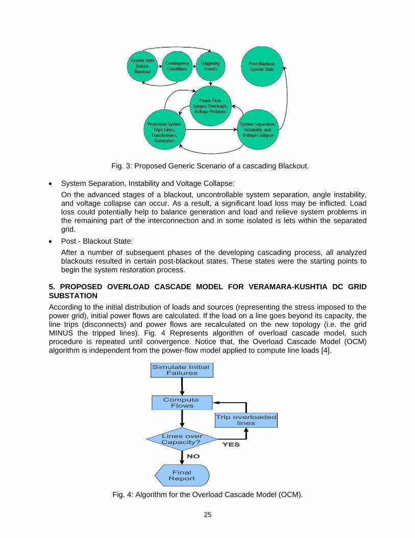
By analyzing these recent blackouts, the following common scenario shows in Fig. 3 of this cascading process can be suggested.
Post Blackout System State:
In all four cases, system parameters remained within their normal operating reliability ranges with no indications of the approaching blackouts. At the same time, some noticeable deviations were observed that could potentially weaken the systems before the actual blackouts.
Contingency Conditions:
Before the blackouts, the systems were additionally weakened by unscheduled outages. These were outages of the transmission lines.
Triggering Events:
At certain point of the blackout developments, a triggering event happened. Triggering events separate a period where multiple “undirected” factors finally contributing but not directly connected to a blackout are accumulated, from the “blackout-directed” sequence of events with clear cause effect relationships between the subsequent phases.
Power Flow Surges, Overloads and Voltage Problems:
The triggering events as well as the subsequent events in a blackout scenario cause power flow surges, overloads, and voltage problems. These problems in their turn are causes of the subsequent events in the sequence. Frequency deviations should be added to this list at the latest phases of the blackout development.
Protection System Trips Lines, Transformers and Generators :
The power system relay protection plays a very important role in a blackout development. Its action could be caused directly by the system problems when the protective relays reacted as if the high flows or low voltages were due to a short circuit, or indirectly, when the system problems cause real short-circuits or instability, e.g., when the overheated conductors contact a tree. The protection system isolates the equipment or a group of equipment from the rest of network. Some load loss may accompany this process. This can result in more power flow surges, overloads, and voltage problems, and so on. It is interesting to notice, that the cascading process can be relatively slow, at least at its initial stages.
25
Fig. 3: Proposed Generic Scenario of a cascading Blackout.
System Separation, Instability and Voltage Collapse:
On the advanced stages of a blackout, uncontrollable system separation, angle instability, and voltage collapse can occur. As a result, a significant load loss may be inflicted. Load loss could potentially help to balance generation and load and relieve system problems in the remaining part of the interconnection and in some isolated is lets within the separated grid.
Post - Blackout State:
After a number of subsequent phases of the developing cascading process, all analyzed blackouts resulted in certain post-blackout states. These states were the starting points to begin the system restoration process.
5. PROPOSED OVERLOAD CASCADE MODEL FOR VERAMARA-KUSHTIA DC GRID
SUBSTATION
According to the initial distribution of loads and sources (representing the stress imposed to the power grid), initial power flows are calculated. If the load on a line goes beyond its capacity, the line trips (disconnects) and power flows are recalculated on the new topology (i.e. the grid MINUS the tripped lines). Fig. 4 Represents algorithm of overload cascade model, such procedure is repeated until convergence. Notice that, the Overload Cascade Model (OCM) algorithm is independent from the power-flow model applied to compute line loads [4].
Fig. 4: Algorithm for the Overload Cascade Model (OCM).

26
6. SUMMARY OF OBSERVATION AND RECOMMENDATION [3, 10-13]
Some observations and recommendations suggested by the Russian emergency control and protection system and different blackouts investigators who analyzed the cause of different blackouts are summarized below:
Develop wide-area coordinated approach to improve the overall security of power grids.
Provide situation awareness tools for TSOs including real time information on the forced outages, status of critical facilities, system topology, and system problems. This includes wide-area system visibility and state estimation including information on the status of the neighboring control areas and dispatcher alarm systems.
Look-ahead vision capabilities including automatic contingency analysis cycling periodically every 5-15 minutes.
Clearly defined and robust interactions between informational, computer, and real-time dispatch services and personnel.
Procedures regulating interactions and coordination between control centers in emergency conditions, preparedness of the dispatch personnel to act in situations where disturbances and violations are in different control areas.
Need in automatic emergency control systems relieving overloads and preventing instabilities, development of the under frequency and under voltage load shedding systems sufficient to prevent uncontrollable cascading, provide integrity of the automatic protection equipment.
Development of controllable system separation schemes to prevent a widespread system failure. This requires advanced measuring and control systems, in which information from several areas and system conditions is integrated [and where control signals initiating line tripping are applied in different control areas] [3].
Need in automation providing survivability of power plants at large power deficiencies in the system. Power stations should disconnect from the grid earlier to go into house-load operation before a system collapse. Provide possibility of restoring voltage from these plants at system black starts.
Attention on design, inspection and preventive maintenance of the system, particularly at vulnerable points with major consequences in the event of a fault.
Achieve better understanding of the nature of cascading failures, develop tools and indicators to detect potential cascading developments and their reasons, work out measures to prevent cascading developments by means of system reinforcements and preventive control [3].
Need to develop protection systems able to detect [and prevent] voltage collapse [as well as frequency, angular, and transient instability] in the entire system.
Development of mandatory reliability standards.
Harmonization of the grid control and protection with the market transactions between the market participants.
7. RECOMMENDATIONS
It’s very tough to observation any critical conditions data to analysis and giving a brief about the realistic recommendations because of very low possibility of getting the faulty time data or any information about the blackout in Bangladesh. Here we represent some recommendations which is representing only from academic studies and observing the above recommendations which have been implemented in different countries already.

27
Ensure the standard operating procedures (SOP) in critical conditions and to trained people with realistic simulations to deal with cascading failures.
Monitoring the whole power system by a specialist team and can be able to access any data from responsible authority to understanding any critical situation.
Improve comprehensive studies on frequency, angular, and transient instability as well as the entire power protection systems which can be able to detect and prevent any kind of voltage collapse.
Attention on design, inspection and preventive maintenance of the system since our whole system is developing continuously.
Increase research in automatic emergency control systems relieving overloads and preventing instabilities.
Development of the under frequency and under voltage load shedding systems sufficient to prevent uncontrollable cascading, provide integrity of the automatic protection equipment by analyzing and comparing with the real data in different critical conditions.
Establish a comprehensive restoration plan.
Improve a standard and realistic grid code or grid law.
Develop a blackout prevention team.
Develop a mandatory reliability of grid substation.
Aware people to use green energy and stop to wasting power energy.
8. CONCLUSION
This recent blackout of Bangladesh is indicates that the country should have sufficient power generation to meet its primary needs and to overcome this power demand Bangladeshi authority has tried to improve its energy situation. In these circumstances a blackout can be a threat to the national security or to the whole power system. One of the main purposes of this paper is to share this mentioned experimental solutions with the Bangladeshis authority with the hope of this summery and recommendations could help to build more secure and smart power grid system in near future and our recommendations will be helpful to prevent blackouts perspective of Bangladesh.
REFERENCES
[1] ‘Nationwide blackout in Bangladesh ends’ By Associated Press, 2 Nov 2014 [Online] Available on: http://www.latimes.com/world/asia/la-fg-nationwide-blackout-in-bangladesh-ends-20141102-story.html
[2] ‘Country faces longest power outage’, Special Correspondent, The Daily Prothom-Alo, November 02, 2014 [Online], Available on: http://en.prothomalo.com/bangladesh/news/55856/Country-faces-longest-power-outage
[3] Yuri V. Makarov, Viktor I. Reshetov, Vladimir A. Stroev, Nikolai I. Voropai “Blackouts in North America and Europe: Analysis and Generalization”, 2005 IEEE St. Petersburg Power Tech, St. Petersburg, Russia, June 27-30, 2005
[4] Sakshi Pahwa, Caterina Scoglio and Antonio Scala ‘Abruptness of Cascade Failures in Power Grids’ Scientific Reports4, Article number: 3694,doi:10.1038/srep03694,[Online],Available on : http://www.nature.com/srep/2014/140115/srep03694/fig_tab/srep03694_F2.html
[5] A tripping in power grid that darkened all, NEWAGE, November 3, 2014 [Online] Available on: http://newagebd.net/63172/a-tripping-in-power-grid-that-darkened all/#sthash.aWKa0uOo.Lo9lGop3.dpbs
[6] Aminur Rahman Rasel ‘Lights out all over Bangladesh’, Dhaka Tribune, November 01, 2014 [Online] Available on : http://www.dhakatribune.com/bangladesh/2014/nov/01/power-outrage-hits-entire-country
29
J. Bangladesh Electron. 14 (1-2); 29-34, 2014
Security Aspects of Re-configurable FPGA based Crypto-system
Mohammad Noor Nabi1, Md. Shafiul Alam2 and Farruk Ahmed1
1School of Engineering and Computer Science, Independent University, Bangladesh, Dhaka, Bangladesh
2Dept. of Electrical and Electronic Engineering, Dhaka University, Dhaka, Bangladesh
[email protected], [email protected], [email protected]
Abstract
The re-configurability of FPGAs makes them better option for system design compared with ASICs, which are costly to develop. The implementation of crypto-system on FPGA is immensely accepted in different research and development forums. FPGAs deliver enhanced performance and modules, like 32-bit soft processors, DSP modules, and high performance interfaces. Recent secure systems use SRAM based FPGAs with few security aspects form manufactures. This paper addresses few security problems of FPGA based design of Crypto-system. In this paper we investigate different security problems in using FPGA for secure system. Few countermeasures are proposed to overcome these security risks.
Keywords: FPGA; Crypto-system; Security; IP.
1. INTRODUCTION
Field Programmable Gate Array (FPGA) is increasingly being used to replace functions performed by ASICs and microprocessors. FPGAs are available with millions of gates which enable embedded ASIC-level functionality. These enhanced functionalities by FPGA make an increasingly popular target for security attack.
The choice of implementation platform for cryptographic applications depends upon many critical factors such as complexity of algorithm and its application area, cost, speed, power consumption and desired security aspects [1][2][3]. FPGAs parallel operations and execution of customized functions make them performance competitive over the sequential microprocessors and microcontrollers [2] [4]. The potential advantages of reconfigurable hardware in cryptographic applications are algorithm agility, algorithm upload, architecture efficiency, resource efficiency, algorithm modification, throughput, cost efficiency [5] [6].
The most common FPGA in use today is SRAM-based with distinct advantage of their flexibility for configuration changes but must be reconfigured every time the FPGA is powered up; this opens up the threat of theft of Intellectual Property (IP) since the system configuration is stored in easy-to-access PROM [7]. The link between PROM and FPGA represents a major security risk. Non-volatile-based FPGA eliminates these security risk but very expensive to use due to its antifuse technology [8]. Other preventive measure with high-end FPGAs have already been extended with symmetric-key decryption engines used to load an encrypted version of the configuration that cannot simply be copied and used without knowledge of the secret key. However, such protection systems based on straightforward use of symmetric cryptography are not well-suited with respect to business and licensing processes, since they are lacking a convenient scheme for key transport and installation [9].
The importance of FPGA design and embedded information being sent to or from a system leads to following aspects: Intellectual-property security to protect vendors own design from being reverse engineered and data security to protect user design from being copied or corrupted [8].
The rest of the chapter is organized as follows: in Sect. II, we describe Security challenges of FPGA based crypto-system and an initial analysis of attacks against FPGAs. In Sect. III, we describe the security requirements for cryptographic modules for Prevention and Avoidance of attacks. In Sect. IV, we evaluate the Difficulty levels to prevent attacks and vulnerabilities of

30
FPGAs. In Sect. V, we describe several countermeasures to overcome security risks. Finally in Sect. VI, we present a number of conclusions.
2. SECURITY CHALLENGES OF FPGA BASED CRYPTO-SYSTEM
Security is becoming since several years a major issue in the domain of embedded systems. The motivation behind the pirates depends on the goal they want to achieve, which can be stealing the IP and mixing with their own IP to develop new system functionality or simply copying a system. The attackers’ power is detailed by IBM [10], Class I (clever outsiders) attackers do not have sufficient knowledge of the system but are often very intelligent; Class II (knowledgeable insiders) attackers have experience and specialized technical education and have expertise with sophisticated tools to analyze parts of a systems; Class III (funded organizations) attackers are able to develop teams of specialists and use the most sophisticated and expensive analysis tools as they have no limitation of money and they are considered to do in-depth analysis of system.
In addition to various attacks reported in [3], [5], [6], [11], [12], [13] our research work considers present technology and tools available to report security challenges of FPGA based crypto-system.
A. Black box Attack
The attacker tries all possible combinations; the algorithm could be realized with laborious efforts and a lot of processor power. Using mathematical techniques such as SAT Solvers can be employed for launching black box attack.
B. Physical Attack
This attack extracts information about algorithms to determine secret keys by probing points inside the chip design. This attack targets parts of the FPGA, which are not available through the normal I/O pins which can be achieved through visual inspections and by tools such as optical microscopes, mechanical probes, Focused Ion Beams, Electron –beam tester.
C. Read-back Attack
Readback feature is provided in most FPGA families to read a configuration out of FPGA for easy debugging. The configuration is read through the JTAG or programming interface in order to obtain secret information. Advance tools for easy debugging such as Xilinx JBitsare required for read back attack implementation.
D. Reverse –Engineering of the Bit Streams
Design of proprietary crypto algorithm or the secret keys can be analyzed by reverse engineering of (unencrypted) bitstream. Simple designs can be understood by cycling through the inputs and reading the outputs. The resourceful pirate may “decap” a chip and microprobe its contents.
E. Side channel attacks
Any physical implementation of a cryptographic system may provide a side channel that leaks information which can be exploited by the attacker to launch this attack. By observing power consumption, timing behavior, and electromagnetic radiation using simple and differential Power analysis (SPA, DPA), simple electro-magnetic analysis (SEMA), differential electro-magnetic analysis (DEMA) side channel information could be exploited to find secret keys from tamper resistant device.
The RSA algorithm is implemented with main usage of squaring and multiplication functions. As reported in the literature, CMOS gates while switching draw current spikes which are exploited using the highly sensitive E & H probes and high end oscilloscope for launching this power analysis attack.
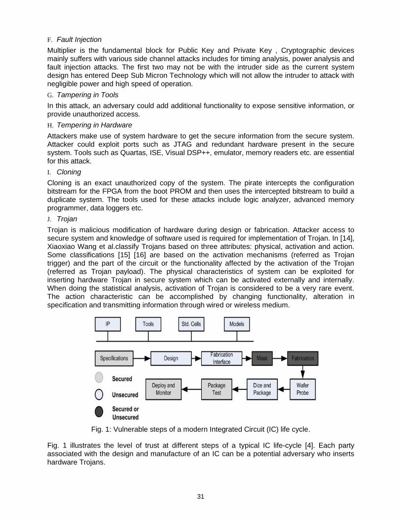
31
F. Fault Injection
Multiplier is the fundamental block for Public Key and Private Key , Cryptographic devices mainly suffers with various side channel attacks includes for timing analysis, power analysis and fault injection attacks. The first two may not be with the intruder side as the current system design has entered Deep Sub Micron Technology which will not allow the intruder to attack with negligible power and high speed of operation.
G. Tampering in Tools
In this attack, an adversary could add additional functionality to expose sensitive information, or provide unauthorized access.
H. Tempering in Hardware
Attackers make use of system hardware to get the secure information from the secure system. Attacker could exploit ports such as JTAG and redundant hardware present in the secure system. Tools such as Quartas, ISE, Visual DSP++, emulator, memory readers etc. are essential for this attack.
I. Cloning
Cloning is an exact unauthorized copy of the system. The pirate intercepts the configuration bitstream for the FPGA from the boot PROM and then uses the intercepted bitstream to build a duplicate system. The tools used for these attacks include logic analyzer, advanced memory programmer, data loggers etc.
J. Trojan
Trojan is malicious modification of hardware during design or fabrication. Attacker access to secure system and knowledge of software used is required for implementation of Trojan. In [14], Xiaoxiao Wang et al.classify Trojans based on three attributes: physical, activation and action. Some classifications [15] [16] are based on the activation mechanisms (referred as Trojan trigger) and the part of the circuit or the functionality affected by the activation of the Trojan (referred as Trojan payload). The physical characteristics of system can be exploited for inserting hardware Trojan in secure system which can be activated externally and internally. When doing the statistical analysis, activation of Trojan is considered to be a very rare event. The action characteristic can be accomplished by changing functionality, alteration in specification and transmitting information through wired or wireless medium.
Fig. 1: Vulnerable steps of a modern Integrated Circuit (IC) life cycle.
Fig. 1 illustrates the level of trust at different steps of a typical IC life-cycle [4]. Each party associated with the design and manufacture of an IC can be a potential adversary who inserts hardware Trojans.
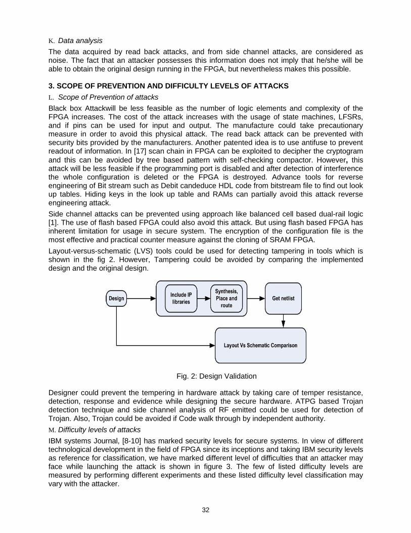
32
K. Data analysis
The data acquired by read back attacks, and from side channel attacks, are considered as noise. The fact that an attacker possesses this information does not imply that he/she will be able to obtain the original design running in the FPGA, but nevertheless makes this possible.
3. SCOPE OF PREVENTION AND DIFFICULTY LEVELS OF ATTACKS
L. Scope of Prevention of attacks
Black box Attackwill be less feasible as the number of logic elements and complexity of the FPGA increases. The cost of the attack increases with the usage of state machines, LFSRs, and if pins can be used for input and output. The manufacture could take precautionary measure in order to avoid this physical attack. The read back attack can be prevented with security bits provided by the manufacturers. Another patented idea is to use antifuse to prevent readout of information. In [17] scan chain in FPGA can be exploited to decipher the cryptogram
and this can be avoided by tree based pattern with self-checking compactor. However, this attack will be less feasible if the programming port is disabled and after detection of interference the whole configuration is deleted or the FPGA is destroyed. Advance tools for reverse engineering of Bit stream such as Debit candeduce HDL code from bitstream file to find out look up tables. Hiding keys in the look up table and RAMs can partially avoid this attack reverse engineering attack.
Side channel attacks can be prevented using approach like balanced cell based dual-rail logic [1]. The use of flash based FPGA could also avoid this attack. But using flash based FPGA has inherent limitation for usage in secure system. The encryption of the configuration file is the most effective and practical counter measure against the cloning of SRAM FPGA.
Layout-versus-schematic (LVS) tools could be used for detecting tampering in tools which is shown in the fig 2. However, Tampering could be avoided by comparing the implemented design and the original design.
Fig. 2: Design Validation
Designer could prevent the tempering in hardware attack by taking care of temper resistance, detection, response and evidence while designing the secure hardware. ATPG based Trojan detection technique and side channel analysis of RF emitted could be used for detection of Trojan. Also, Trojan could be avoided if Code walk through by independent authority.
M. Difficulty levels of attacks
IBM systems Journal, [8-10] has marked security levels for secure systems. In view of different technological development in the field of FPGA since its inceptions and taking IBM security levels as reference for classification, we have marked different level of difficulties that an attacker may face while launching the attack is shown in figure 3. The few of listed difficulty levels are measured by performing different experiments and these listed difficulty level classification may vary with the attacker.

33
Fig. 3: Difficulty levels of different attacks
4. PROPOSED MEASURES TO OVERCOME SECURITY RISKS
In this section we summarize few countermeasures to minimize the effects of the previously mentioned attacks. There is no upper limit on the level of security that can be achieved, some of key features which should be incorporated during programming phase of FPGA based secure systems have been suggested.
A. Encryption of the configuration file is the most effective and practical countermeasures against the cloning and reverse engineering of SRAM FPGA design, PROM should store only the encrypted bitstream file and also there should be feature of on-chip bit stream decryption. Now days, vendors are providing these features with 3- DES implementation for bit stream encryption [19]. Designer should include dummy cycles while doing cryptographic operation.
B. The design should have provision of software or hardware countermeasure for all the side channel attacks. For software countermeasures, design should mask secret key with the random values.
C. The final implemented design and original design should be checked for their equivalence to avoid the tampering in original design by the design tools. This must be incorporated in the validation stage of development cycle.
D. FPGA has to be embedded into a secure environment and designer should include the feature such as deletion of bitstream when tempering is detected. This eventually will prevent readback and fault injection attack
E. The designer should implement all critical parts of the design with minimum three level of modular redundancy (MR). In case of physical compromise of the system, the designer should incorporate the feature of self destruction of the system. For example, with the detection of unauthorized interference, system design should be such that it erases the firmware & secret key information from the system.
F. A cryptographic module shall perform power-up self-tests and conditional self-tests to ensure that the module is functioning properly. The designers should give due consideration to make all unused I/O pins/ports as tri state so that unauthorized access could be avoided.
G. The design of FPGA should be such that provision of maintaining keys by the user must be avoided in order to cater for future changes in the design of secure systems.
H. Key length of 128 bits for AES, 160 bits for ECC, 1024 bits for RSA possesses strength to avoid Black Box attack in FPGA based secure systems. [20]
0 1 2 3 4 5 6
Black Box Attack
Read baCK Attack
Cloning-Flash FPGA
Cloning-Antifuse
SRAM FPGA With Encryption
SRAM FPGA
Reverse Engineering
Physical Attack
Side Channel Attacks
Tampering in tools
Fault Attack
Tempering in Hardware
Data Analysis
Trojan
Difficulty Level
(in scale 1-5 with 5 as maximum level of difficulty)
34
I. Customized FPGA based board for cryptographic applications so that minimum resources with actual use should be included in the hardware.
J. Physical/logical separation should be incorporated for plain and cipher data at design level.
K. Few significant countermeasures strategies have been proposed in [21], includes clock randomization, power consumption randomization or compensation and tamper detection.
5. CONCLUSION
FPGA based crypto-systems’ design security must be part of the design process not an afterthought since attacks against these systems are becoming more critical and sophisticated. The FPGA design and implementation flow is separate and steps must be required so that sensitive design is not exposed to theft and tempered through manufacturing process. In this paper, we have emphasized current vulnerabilities of FPGAs at all the levels of the security pyramid and presented numerous nooks for improvement.
We have pointed out the difficulty levels which may vary with the class of attacker and development of technological tools. This paper addresses all the possible vulnerabilities but sill this area is open for research due to latest developments of sophisticated tools and hardware. Most of the countermeasures are currently under definition or under implementation. The next step of the research is to prototype these countermeasures to evaluate their effectiveness for compliance of the security standards.
REFERENCES
[1] D.P. Wilt, R.C. Meitzler, and J.P. DeVale. Metrics for TRUST in Integrated Circuits, 2008G.
[2] A. Elbirt, W. Yip, B. Chetwynd, and C. Paar. An FPGA-based performance Evaluation of the AES block cipher candidate algorithm finalists. IEEE Transactions on VLSI Design, 9(4):545{557, August 2001.
[3] A. Ross. Security Engineering, A Guide to Building Dependable Distributed Systems. Wiley, New York, second edition edition, 2008.
[4] DARPA, “TRUST in Integrated Circuits (TIC) - Proposer Information Pamphlet”, 2007. [Online]. Available: http://www.darpa.mil/MTO/ solicitations/baa07-24/index.html
[5] T. Wollinger and C. Paar. How Secure Are FPGAs in Crypto-graphic Applications?(Long Version).Report 2003/119,IACR,2003.
[6] T. Wollinger, J. Guajardo and C. Paar ― Security on FPGAs: State of the Art Implementations and Attacks ACM Special Issue Security and Embedded Systems Vol. No. March 2003.
[7] White paper “FPGA Design Security Issues: Using the ispXPGA Family of FPGAs to Achieve High Design Security” Lattice Semiconductor Corporation, December 2003.
[8] Actel Corporation www.actel.com,―Design Security in Nonvolatile Flash and Antifuse FPGAs, Security Backgrounder ©2002.
[9] Dynamic Intellectual Property Protection for Reconfigurable Devices Tim uneysu, Bodo Moller, Christof PaarHorst Gortz Institute for IT Security, Ruhr-Universitt Bochum, Germany{gueneysu,bmoeller,cpaar}@crypto.rub.de
[10] http://www.bltinc.com/services .fpga-reverseengineering.htm. FPGA Reverse Engineering Services.
[11] E. J. Chikofsky and J. H. Cross, II, ―Reverse Engineering and Design Recovery, IEEE Software, vol. 7, no. 1, pp. 13-17, January 1990.
[12] A Baumgarten et al ―A case study of hardware Trojan design and implementation Springer-Verlag 2010
35
J. Bangladesh Electron. 14 (1-2); 35-42, 2014
Parametric Study On Subwavelength Plasmonic Nanostructure
For Enhanced Optical Transmission
Md. Zahir Uddin Suja, Sunayna Binte Bashar, M. L. Palash and Subrata Das
Dept. of Electrical and Electronic Engineering, University of Dhaka, Dhaka Bangladesh e-mail:[email protected], [email protected], [email protected], [email protected]
Abstract
This work deals with one of the astonishing property of light propagation through subwavelength aperture array i.e. the enhanced optical transmission (EOT). The design, construction and simulation of metallic nanostructure have been studied well within visible region (441 THz) to generate the transmission spectrum. An array of square subwavelength apertures in gold (Au) film deposited on SiO2 substrate has been designed with commercial simulation software optiFDTDTM 10 to observe the enhanced optical transmission. The EOT through this periodic subwavelength aperture depends on several parameters. Among those parameters - lattice periodicity, aperture width, metal thickness and refractive index (RI) of the surface dielectric medium were our point of interest. The parametric study on EOT has been performed on that designed structure and both quantitative and qualitative analyses have been addressed. Among the observations, the most important implication is that EOT has linear dependency on the aperture width and metal thickness. The transmission efficiency falls about 76% when the gold thickness varied from 100 nm to 250 nm with constant aperture width of 200 nm. This indicates that metal thickness is the most prominent factor in enhanced transmission. The study on the complicated nature of these generated spectra could provide significant insight into the use of these films for displays, spectroscopic substrates, or near-field parallel imaging arrays.
Keywords: Nanostructure, Plasmonic, Enhanced Optical Transmission, Subwavelength
1. INTRODUCTION
Surface plasmon polaritons (SPPs) are electromagnetic modes that arise from the interaction between light and mobile surface charges, typically the conduction electrons in metals. This light-matter interaction leads to SPP modes having greater momentum than light of the same frequency; consequently the electromagnetic fields associated with them cannot propagate away from the surface: rather, the field decays exponentially in strength with distance away from the surface [1-3]. This effect leads to the highly challenging applications in the present era like plasmonic enhancement of fluorescence for sensor applications [4], plasmonic thin-film solar cells with broadband absorption enhancements [5], and plasmonic structures for chemical and biological sensing applications [6] etc. A very interesting effect of light interacting with structured metals has been observed very recently: the transmission of light through subwavelength hole arrays made in a metal film can be orders of
magnitude larger than expected from standard aperture theory [7].The enhancement results from the light coupling with the surface waves along the aperture array structure [8]. The surface plasmon modes along the metal interface have significant roles in the high transmission spectra. The excited surface plasmon modes are caused by the momentum conservation of the incident light’s wave vector with the two dimensional grating wave vectors which result from the periodic structure.
The study of the extraordinary optical transmission through subwavelength small metallic hole arrays has been active since the first observation by the Ebbesen group at 1998 [9]. Ebbesen et al. have addressed the issue of thickness as being a determining factor in transmission spectra but they comment that the periodicity of the array determines the peak positions and that the features can be appreciably effected by the type of lattice (i.e., square or triangular lattice) [10].

36
Moreover dependence of enhanced transmission on refractive index of the medium surrounding the nanostructures has been predicted [7]. But a complete picture of the dependence of enhanced optical transmission on various parameters is yet to be elucidated. The present work is thus an attempt to sort out these limitations on parametric dependence of enhanced optical transmission through periodic subwavelength apertures. So to understand this parametric dependency an array of square subwavelength aperture in gold (Au) film deposited in SiO2 substrate, as shown in Figure 1, is considered under this work. The enhanced transmission spectrum generated from the parametric variations is also studied to get a vivid picture of this dependency. The simulation of the designed structure is carried out by OptiFDTD10 [11].
(a) (b)
Fig. 1: (a): Schematic of a unit cell, (b) Schematic of an array of square subwavelength aperture.
2. SIMULATION OF THE DESIGN STRUCTURE
As outlined in [3], the required initial conditions for obtaining plasmonic effect are tabulated in Table 1. A Gaussian modulated continuous wave with the following parameters listed in Table 2 is utilized in the simulation. Each transmission spectrum is evaluated in the wavelength range 500-1000 nm.
Table 1: Initial value of the design parameter
Aperture Shape Square
Aperture Width 200 nm
Periodicity of the array 400 nm
Thickness of the gold layer 200 nm
Dielectric medium of the surface (aperture) Air (n=1)
Dielectric medium of the background (substrate) SiO2 (n=1.5)
Let us consider first the planar metallic structure without any subwavelength aperture. This will help us to realize the enhanced optical transmission property of the periodic subwavelength apertures. A 200 nm gold metal layer deposited on SiO2 substrate to generate the transmission spectrum has been considered.
Table 2: Parameters of input light wave signal
Center Wavelength 680 nm
Center Frequency 441 THz
Input Field Transverse Rectangular
Polarization TM
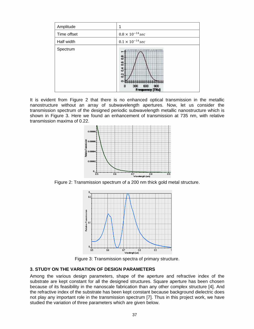
37
Amplitude 1
Time offset 0.8 × 10⁻¹⁴𝑠𝑒𝑐
Half width 0.1 × 10⁻¹⁴𝑠𝑒𝑐
Spectrum
It is evident from Figure 2 that there is no enhanced optical transmission in the metallic nanostructure without an array of subwavelength apertures. Now, let us consider the transmission spectrum of the designed periodic subwavelength metallic nanostructure which is shown in Figure 3. Here we found an enhancement of transmission at 735 nm, with relative transmission maxima of 0.22.
Figure 2: Transmission spectrum of a 200 nm thick gold metal structure.
Figure 3: Transmission spectra of primary structure.
3. STUDY ON THE VARIATION OF DESIGN PARAMETERS
Among the various design parameters, shape of the aperture and refractive index of the substrate are kept constant for all the designed structures. Square aperture has been chosen because of its feasibility in the nanoscale fabrication than any other complex structure [4]. And the refractive index of the substrate has been kept constant because background dielectric does not play any important role in the transmission spectrum [7]. Thus in this project work, we have studied the variation of three parameters which are given below.
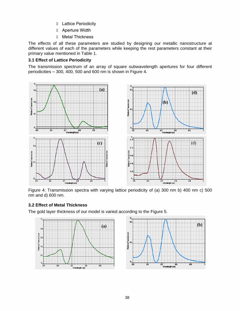
38
Lattice Periodicity
Aperture Width
Metal Thickness
The effects of all these parameters are studied by designing our metallic nanostructure at different values of each of the parameters while keeping the rest parameters constant at their primary value mentioned in Table 1.
3.1 Effect of Lattice Periodicity
The transmission spectrum of an array of square subwavelength apertures for four different periodicities – 300, 400, 500 and 600 nm is shown in Figure 4.
Figure 4: Transmission spectra with varying lattice periodicity of (a) 300 nm b) 400 nm c) 500 nm and d) 600 nm.
3.2 Effect of Metal Thickness
The gold layer thickness of our model is varied according to the Figure 5.
(a)
(d)
(b)
(c)
(d)
(a) (b)
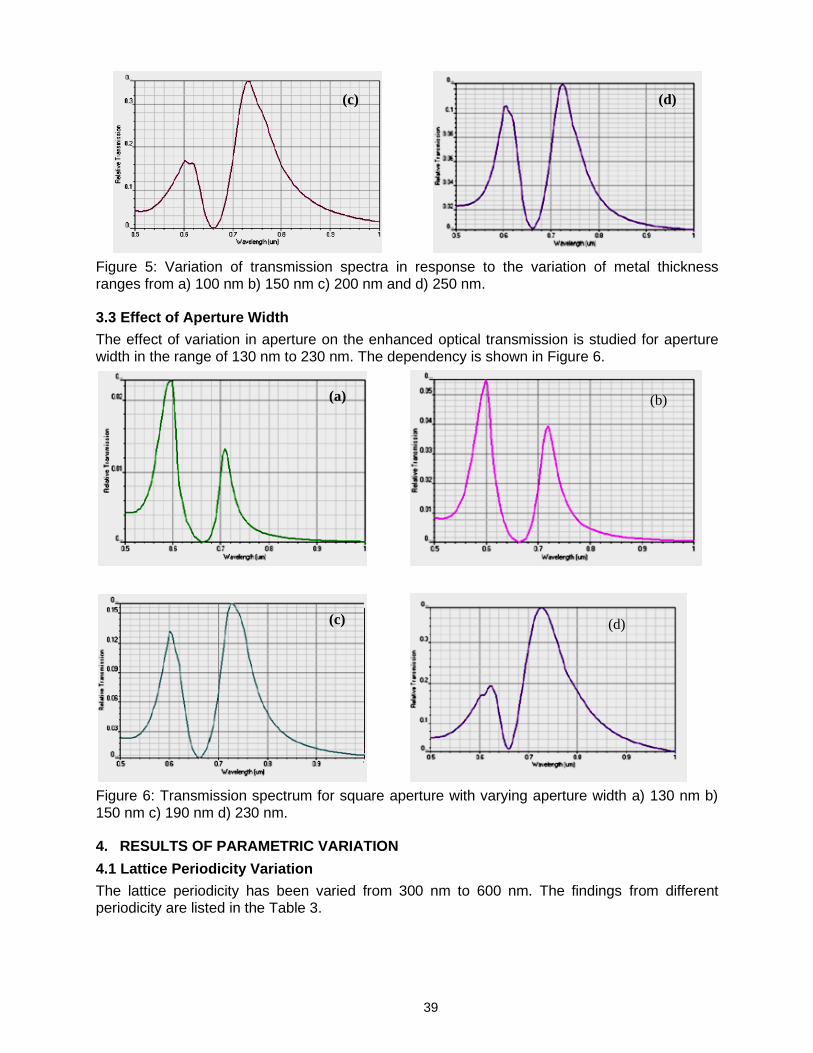
39
Figure 5: Variation of transmission spectra in response to the variation of metal thickness ranges from a) 100 nm b) 150 nm c) 200 nm and d) 250 nm.
3.3 Effect of Aperture Width
The effect of variation in aperture on the enhanced optical transmission is studied for aperture width in the range of 130 nm to 230 nm. The dependency is shown in Figure 6.
Figure 6: Transmission spectrum for square aperture with varying aperture width a) 130 nm b) 150 nm c) 190 nm d) 230 nm.
4. RESULTS OF PARAMETRIC VARIATION
4.1 Lattice Periodicity Variation
The lattice periodicity has been varied from 300 nm to 600 nm. The findings from different periodicity are listed in the Table 3.
(d)
(b) (a)
(c) (d)
(c)

40
Table 3: Results obtained for the variation in periodicity of the subwavelength aperture array
Period (nm) 300 400 500 600
Peak wavelength (nm) 620 730 675 650
Relative Transmission 0.35 0.22 0.248 0.159
From the comparison among different periodicities of the array, it is obvious that the most enhanced optical transmission through subwavelength aperture arrays has been achieved for the period of 300 nm. So this periodicity is suitable for enhanced optical transmission than the others. A plot to show the dependency of the periodicity on the EOT is shown in Figure 7.
Figure 7: Dependence of relative transmission on lattice periodicity.
4.2 Effect of Aperture Width
The variation in the aperture width also affects the enhanced optical transmission. The aperture width of the gold metal has been varied in a range of 130 nm to 230 nm. The findings are listed in Table 4.
Table 4: Result obtained for the variation in aperture width
Aperture Width (nm) 130 150 190 230
Peak Wavelength (nm) 600 600 730 730
Relative Transmission 0.023 0.0544 0.159 0.384
The values are then plotted in Figure 8, from where it can be inferred that the relative transmission increases with the increase of aperture width. Further the peak positions are shifted to the longer wavelength as the aperture width increases.
Figure 8: Dependence of relative transmission on aperture width
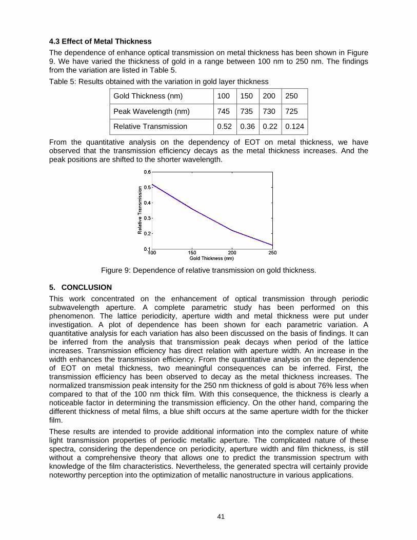
41
4.3 Effect of Metal Thickness
The dependence of enhance optical transmission on metal thickness has been shown in Figure 9. We have varied the thickness of gold in a range between 100 nm to 250 nm. The findings from the variation are listed in Table 5.
Table 5: Results obtained with the variation in gold layer thickness
Gold Thickness (nm) 100 150 200 250
Peak Wavelength (nm) 745 735 730 725
Relative Transmission 0.52 0.36 0.22 0.124
From the quantitative analysis on the dependency of EOT on metal thickness, we have observed that the transmission efficiency decays as the metal thickness increases. And the peak positions are shifted to the shorter wavelength.
Figure 9: Dependence of relative transmission on gold thickness.
5. CONCLUSION
This work concentrated on the enhancement of optical transmission through periodic subwavelength aperture. A complete parametric study has been performed on this phenomenon. The lattice periodicity, aperture width and metal thickness were put under investigation. A plot of dependence has been shown for each parametric variation. A quantitative analysis for each variation has also been discussed on the basis of findings. It can be inferred from the analysis that transmission peak decays when period of the lattice increases. Transmission efficiency has direct relation with aperture width. An increase in the width enhances the transmission efficiency. From the quantitative analysis on the dependence of EOT on metal thickness, two meaningful consequences can be inferred. First, the transmission efficiency has been observed to decay as the metal thickness increases. The normalized transmission peak intensity for the 250 nm thickness of gold is about 76% less when compared to that of the 100 nm thick film. With this consequence, the thickness is clearly a noticeable factor in determining the transmission efficiency. On the other hand, comparing the different thickness of metal films, a blue shift occurs at the same aperture width for the thicker film.
These results are intended to provide additional information into the complex nature of white light transmission properties of periodic metallic aperture. The complicated nature of these spectra, considering the dependence on periodicity, aperture width and film thickness, is still without a comprehensive theory that allows one to predict the transmission spectrum with knowledge of the film characteristics. Nevertheless, the generated spectra will certainly provide noteworthy perception into the optimization of metallic nanostructure in various applications.

42
REFERENCES
[1] W. L. Barnes, "Surface plasmon–polariton length scales: a route to sub-wavelength optics," J. Opt. A: Pure Appl. Opt., vol. 8, pp. S87-S93, 2006.
[2] E Yablonovitch, K.M. Leung, "Hope for photonic bandgaps," Nature, vol. 351, p. 278, 1991.
[3] S. A. Maier, Plasmonics: Fundamental and Applications. New York, USA: Springer,
[4] O. Stranik, H.M. McEvoy, C. McDonagh, B.D. MacCraith, "Plasmonic enhancement of fluorescence for sensor applications," Elsevier Sensors and Actuators, vol. B 107, pp. 148-153, 2005.
[5] Ragip A. Pala, Justin White, Edward Barnard, John Liu and Mark L. Brongersma, "Design of Plasmonic Thin-Film Solar Cells with Broadband Absorption Enhancements," Adv. Mater, vol. 21, pp. 3504-3509, 2009.
[6] Anuj Dhawan, Michael D. Gerhold and John F. Muth, "Plasmonic Structures Based on Subwavelength Apertures for Chemical and Biological Sensing Applications," IEEE Sensors Journal, vol. 8, no. 6, Jun. 2008.
[7] H. A. Bethe, "Theory of diffraction by small holes," Phys. Rev., vol. 66, pp. 163-182, 1944.
[8] Je Hong Kim and P. J. Moyer, "Thickness effects on the optical transmission characteristics of small hole arrays on thin gold films," Opt. Express, vol. 14, pp. 6595-6602, 2006.
[9] A Degiron and T W Ebbesen, "The role of localized surface plasmon modes in the enhanced transmission of periodic subwavelength apertures," J. Opt. A: Pure Appl. Opt., vol. 7, pp. S90-S96, 2005.
[10] T. W. Ebbesen, H. J. Lezec, H. F. Ghaemi, T. Thio and P. A. Wolff, "Extraordinary optical transmission through sub-wavelength hole arrays," Nature, vol. 391, pp. 667-669, 1998.
[11] http://www.optiwave.com/products/fdtd_overview.html
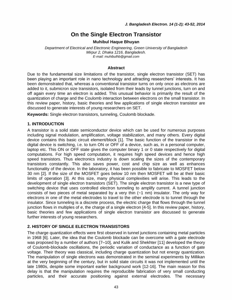
43
J. Bangladesh Electron. 14 (1-2); 43-52, 2014
On the Single Electron Transistor
Muhibul Haque Bhuyan
Department of Electrical and Electronic Engineering, Green University of Bangladesh Mirpur 2, Dhaka 1216, Bangladesh.
E-mail: [email protected]
Abstract
Due to the fundamental size limitations of the transistor, single electron transistor (SET) has been playing an important role in nano technology and attracting researchers’ interests. It has been demonstrated that, whereas a conventional transistor turns on only once as electrons are added to it, submicron size transistors, isolated from their leads by tunnel junctions, turn on and off again every time an electron is added. This unusual behavior is primarily the result of the quantization of charge and the Coulomb interaction between electrons on the small transistor. In this review paper, history, basic theories and few applications of single electron transistor are discussed to generate interests of young researchers on SET.
Keywords: Single electron transistors, tunneling, Coulomb blockade.
1. INTRODUCTION
A transistor is a solid state semiconductor device which can be used for numerous purposes including signal modulation, amplification, voltage stabilization, and many others. Every digital device contains this basic circuit element/block [1]. The basic function of the transistor in the digital device is switching, i.e. to turn ON or OFF of a device, such as, in a personal computer, laptop etc. This ON or OFF state gives the computer binary 1 or 0 state respectively for digital computations. For high speed computation, it requires high speed devices and hence high speed transistors. Thus electronics industry is down scaling the sizes of the contemporary transistors constantly. This also saves power, cost and chip size as well as enhances functionality of the device. In the laboratory, it has been possible to fabricate to MOSFET below 30 nm [2]. If the size of the MOSFET goes below 10 nm then MOSFET will be at their basic limits of operation [3]. At this size, many physical complexities will arise. This leads to the development of single electron transistors (SET). The single electron transistor is a new type of switching device that uses controlled electron tunneling to amplify current. A tunnel junction consists of two pieces of metal separated by a very thin (~1 nm) insulator. The only way for electrons in one of the metal electrodes to travel to the other electrode is to tunnel through the insulator. Since tunneling is a discrete process, the electric charge that flows through the tunnel junction flows in multiples of e, the charge of a single electron [4-5]. In this review paper, history, basic theories and few applications of single electron transistor are discussed to generate further interests of young researchers.
2. HISTORY OF SINGLE ELECTRON TRANSISTORS
The charge quantization effects were first observed in tunnel junctions containing metal particles in 1968 [6]. Later, the idea that the Coulomb blockade can be overcome with a gate electrode was proposed by a number of authors [7–10], and Kulik and Shekhter [11] developed the theory of Coulomb-blockade oscillations, the periodic variation of conductance as a function of gate voltage. Their theory was classical, including charge quantization but not energy quantization. The manipulation of single electrons was demonstrated in the seminal experiments by Millikan at the very beginning of the century, but in solid state circuits it was not implemented until the late 1980s, despite some important earlier background work [12-16]. The main reason for this delay is that the manipulation requires the reproducible fabrication of very small conducting particles, and their accurate positioning against external electrodes. The necessary

44
nanofabrication techniques have become available during the past two decades, and have made possible a new field of solid state physics, single-electronics [17-19]. However, it was not until 1987 that Fulton and Dolan [20] made the first SET, entirely out of metals, and observed the predicted oscillations. They made a metal particle connected to two metal leads by tunnel junctions, all on top of an insulator with a gate electrode underneath. Since then, the capacitances of such metal SETs have been reduced to produce very precise charge quantization.
The first semiconductor SET was fabricated accidentally in 1989 by Scott-Thomas et al. [21] in narrow Si field effect transistors. In this case the tunnel barriers were produced by interface charges. Shortly thereafter Meirav et al. [22] made controlled devices of the kind depicted in Fig. 1, albeit with an unusual heterostructure with AlGaAs on the bottom instead of the top. In these and similar devices the effects of energy quantization were easily observed. [23–25]. Only in the past few years have metal SETs been made small enough to observe energy quantization [26]. Foxman et al. [24] also measured the level width Γ and showed how the energy and charge quantization are lost as the resistance decreases toward h/e2. In most cases, the potential confining the electrons in a SET is of sufficiently low symmetry that one is in the regime of quantum chaos: the only quantity that is quantized is the energy.
The evolution of Coulombic charging peaks with magnetic field has been interpreted with various degrees of sophistication, imitating the development of the theory of atoms. First one tries the “constant interaction model” in which electrons are treated as independent except for a constant Coulombic charging energy. This gives only a qualitative picture of the physics. In order to be quantitative, one needs to at least treat the electron-electron interactions self-consistently (analogous to the Thomas-Fermi model) [27], and for some cases one needs to include exchange and correlations.
In particular, it is found that electrons in an SET undergo a series of phase transitions at high magnetic field. [28]. One of these is well described by Hartree-Fock theory, but others appear to require additional correlations.
The future of research on SETs looks very bright. There are strong efforts around the world to make the artificial atoms in SETs smaller, in order to raise the temperature at which charge quantization can be observed. These involve self-assembly techniques [29] and novel lithographic and oxidation methods [30] whereby artificial atoms can be made nearly as small as natural ones. This is, of course, driven by an interest in using SETs for practical applications. However, as SETs get smaller, all of their energy scales can be larger, so it is very likely that new phenomena will emerge.
3. OPERATION OF SINGLE ELECTRON TRANSISTORS
The conventional field effect transistors are almost completely classical in their physics. Only a few numbers of these transistors that characterize their behavior quantum mechanically. In these transistors all electrons work together. But in single electronic transistor, it is possible to control the movement and position of a single or a very small number of electrons. To understand how a single electron can be controlled, one must understand the movement of electric charge through a conductor. An electric current can flow through the conductor because some electrons are free to move through the lattice of atomic nuclei. The current is determined by the charge transferred through the conductor. Surprisingly this transferred charge can have practically any value, in particular, a fraction of the charge of a single electron. Hence, it is not quantized. The behavior of this type of device is entirely quantum mechanical. This, at first glance counterintuitive fact, is a consequence of the displacement of the electron cloud against the lattice of atoms. This shift can be changed continuously and thus the transferred charge is a continuous quantity. If a tunnel junction interrupts an ordinary conductor, electric charge will move through the system by both a continuous and discrete process. Since only discrete electrons can tunnel through junctions, charge will accumulate at the surface of the electrode against the isolating layer, until a high enough bias has built up across the tunnel junction as
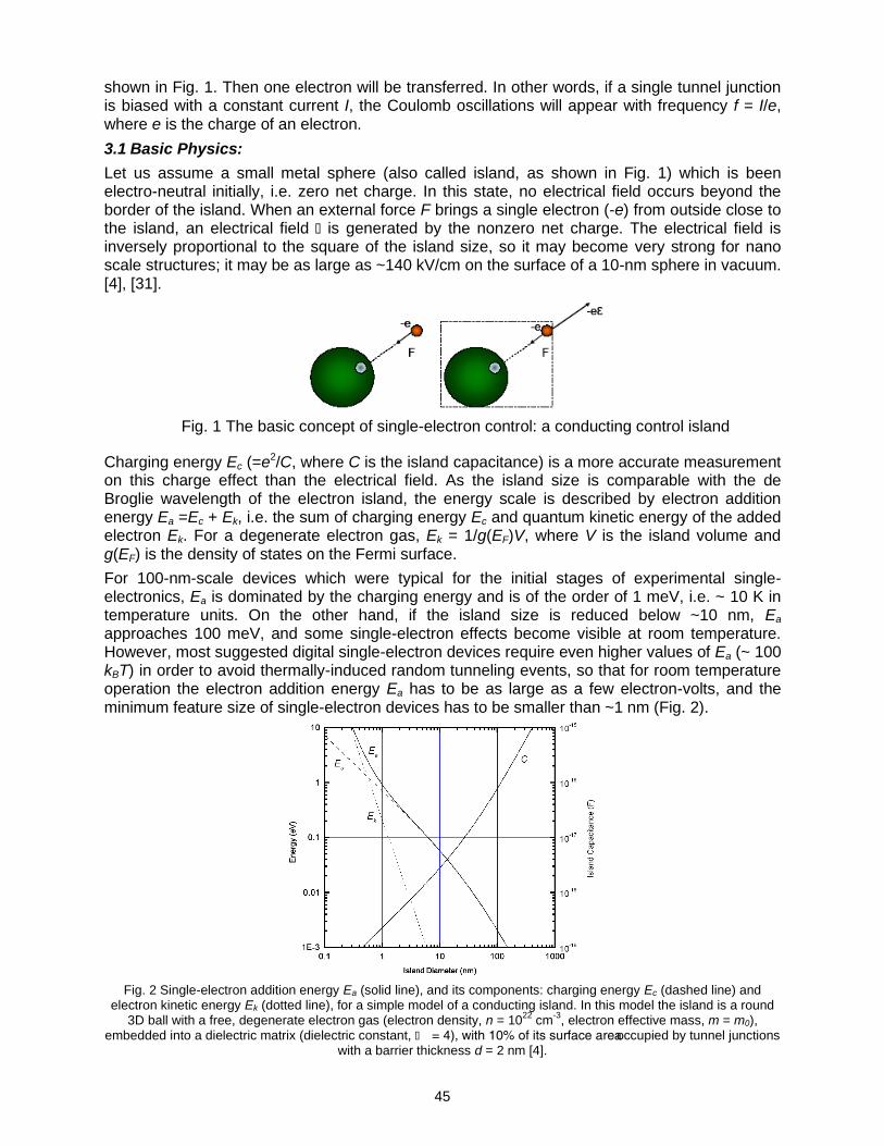
45
shown in Fig. 1. Then one electron will be transferred. In other words, if a single tunnel junction is biased with a constant current I, the Coulomb oscillations will appear with frequency f = I/e, where e is the charge of an electron.
3.1 Basic Physics:
Let us assume a small metal sphere (also called island, as shown in Fig. 1) which is been electro-neutral initially, i.e. zero net charge. In this state, no electrical field occurs beyond the border of the island. When an external force F brings a single electron (-e) from outside close to the island, an electrical field is generated by the nonzero net charge. The electrical field is inversely proportional to the square of the island size, so it may become very strong for nano scale structures; it may be as large as ~140 kV/cm on the surface of a 10-nm sphere in vacuum. [4], [31].
Fig. 1 The basic concept of single-electron control: a conducting control island
Charging energy Ec (=e2/C, where C is the island capacitance) is a more accurate measurement on this charge effect than the electrical field. As the island size is comparable with the de Broglie wavelength of the electron island, the energy scale is described by electron addition energy Ea =Ec + Ek, i.e. the sum of charging energy Ec and quantum kinetic energy of the added electron Ek. For a degenerate electron gas, Ek = 1/g(EF)V, where V is the island volume and g(EF) is the density of states on the Fermi surface.
For 100-nm-scale devices which were typical for the initial stages of experimental single-electronics, Ea is dominated by the charging energy and is of the order of 1 meV, i.e. ~ 10 K in temperature units. On the other hand, if the island size is reduced below ~10 nm, Ea approaches 100 meV, and some single-electron effects become visible at room temperature. However, most suggested digital single-electron devices require even higher values of Ea (~ 100 kBT) in order to avoid thermally-induced random tunneling events, so that for room temperature operation the electron addition energy Ea has to be as large as a few electron-volts, and the minimum feature size of single-electron devices has to be smaller than ~1 nm (Fig. 2).
Fig. 2 Single-electron addition energy Ea (solid line), and its components: charging energy Ec (dashed line) and
electron kinetic energy Ek (dotted line), for a simple model of a conducting island. In this model the island is a round 3D ball with a free, degenerate electron gas (electron density, n = 10
22 cm
-3, electron effective mass, m = m0),
embedded into a dielectric matrix (dielectric constant, = 4), with 10% of its surface area occupied by tunnel junctions with a barrier thickness d = 2 nm [4].

46
In this size range the electron quantization energy Ek becomes comparable with or larger than the charging energy Ea for most materials; this is why these small islands are frequently called ‘quantum dots’. Their use involves not only extremely difficult nanofabrication technology (especially challenging for large scale integration), but also some major physics problems including the high sensitivity of transport properties to small variations of the quantum dot size and shape. This is why it is very important to develop single-electron devices capable of operating with the lowest possible ratio of Ea/kBT.
3.2 Orthodox theory:
In [18], an orthodox theory of single-electron tunneling has been formulated. This theory plays an important guiding role in the history of single-electronics. Kulik and Shekhter are the pioneer of this theory [11]. The theory makes the following major assumptions:
The electron energy quantization inside the conductors is ignored, i.e. the electron energy spectrum is treated as continuous. It is valid if Ek << kBT as long as Ek << Ec.
The time of electron tunneling through the barrier is assumed to be negligibly small in comparison with other time scales. It is valid for tunnel barriers used in single-electron devices of practical interest, where tunneling time is of the order of ~ 10-15 s.
Coherent quantum processes consisting of several simultaneous tunneling events (co-tunneling) are ignored. This assumption is valid if the resistance R of all the tunnel barriers of the system is much higher than the quantum unit of resistance RQ, i.e.,
R >> RQ, RQ = h/4e2 6.5 KΔ
The latter relation is of principal importance for single-electronics as a whole.
Despite the limitations listed above, the orthodox theory is in quantitative agreement with virtually all the experimental data for systems with metallic conductors (with their small values of the electron wavelength on the Fermi surface) and gives at least a qualitative description of most results for most semiconductor structures (where the quantization effects are more noticeable, due to larger Fermi surface). The main result of the theory can be formulated as follows:
The tunneling of a single electron through a particular tunnel barrier is always a random event, with a certain rate Δ (i.e. probability per unit time) which depends solely on the reduction of ΔW of the free (electrostatic) energy of the system as a result of this tunneling event as in Fig. 3 (a). Within the orthodox theory this dependence may be expressed with a universal formula given in equation (1).
11
1 BW k TWW I e
e e
(1)
where I(V) is the "seed" dc I-V curve of the tunnel barrier in the absence of single-electron charging effects. ΔW can be written from the system's electrostatics as given in equation (2).
2
i fV VW e
(2)
where Vi and Vf are voltage drops across the barrier before and after the tunneling event.
Figure 3 (b) shows the dependence given by equation (1); at low temperatures (i.e. when kBT << ΔW) only tunneling events decreasing the electrostatic energy (and dissipating the difference) are possible, and their rate is proportional to ΔW. An increase in applied voltage increases the number of electron states in the source electrode which may provide an electron capable of tunneling into an empty state of the drain electrode.
Though equations (1) and (2) are rather simple, the calculation of properties of even some basic single-electron systems runs into a technical problem. In many situations, several tunneling events are possible at the same time, and the orthodox theory only gives the chances of a particular outcome. Hence, some sort of statistical calculation scheme may be required. For
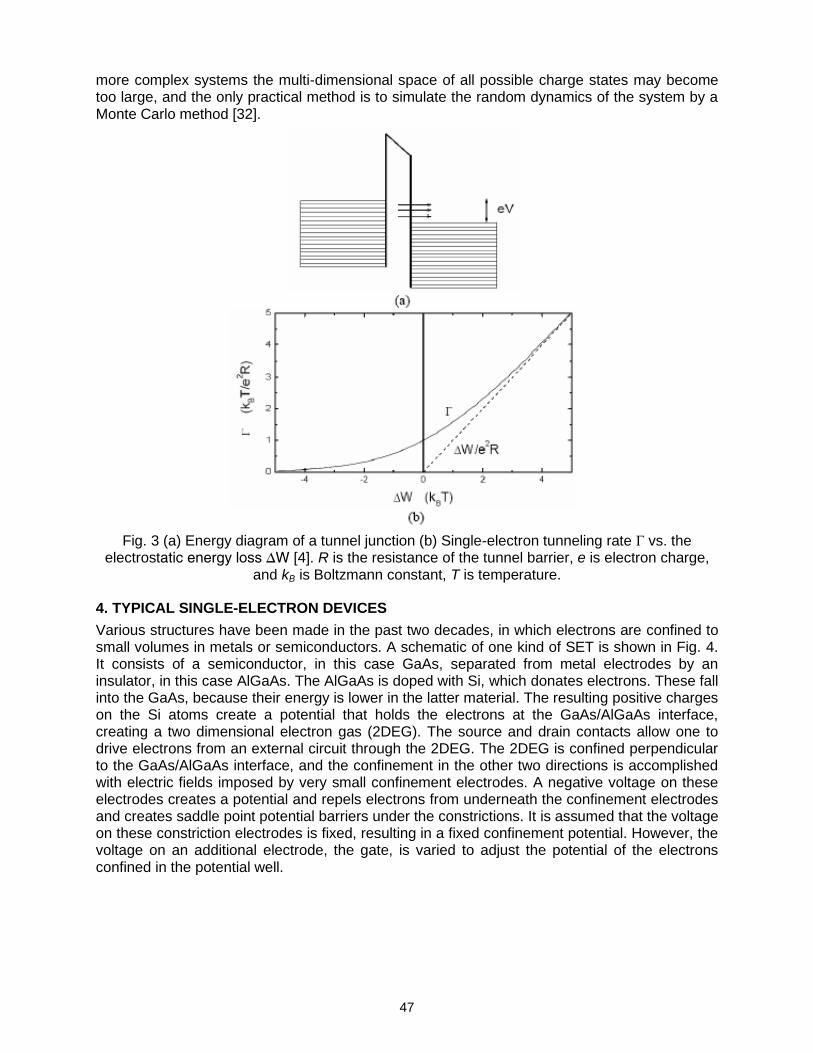
47
more complex systems the multi-dimensional space of all possible charge states may become too large, and the only practical method is to simulate the random dynamics of the system by a Monte Carlo method [32].
Fig. 3 (a) Energy diagram of a tunnel junction (b) Single-electron tunneling rate Γ vs. the electrostatic energy loss ∆W [4]. R is the resistance of the tunnel barrier, e is electron charge,
and kB is Boltzmann constant, T is temperature.
4. TYPICAL SINGLE-ELECTRON DEVICES
Various structures have been made in the past two decades, in which electrons are confined to small volumes in metals or semiconductors. A schematic of one kind of SET is shown in Fig. 4. It consists of a semiconductor, in this case GaAs, separated from metal electrodes by an insulator, in this case AlGaAs. The AlGaAs is doped with Si, which donates electrons. These fall into the GaAs, because their energy is lower in the latter material. The resulting positive charges on the Si atoms create a potential that holds the electrons at the GaAs/AlGaAs interface, creating a two dimensional electron gas (2DEG). The source and drain contacts allow one to drive electrons from an external circuit through the 2DEG. The 2DEG is confined perpendicular to the GaAs/AlGaAs interface, and the confinement in the other two directions is accomplished with electric fields imposed by very small confinement electrodes. A negative voltage on these electrodes creates a potential and repels electrons from underneath the confinement electrodes and creates saddle point potential barriers under the constrictions. It is assumed that the voltage on these constriction electrodes is fixed, resulting in a fixed confinement potential. However, the voltage on an additional electrode, the gate, is varied to adjust the potential of the electrons confined in the potential well.
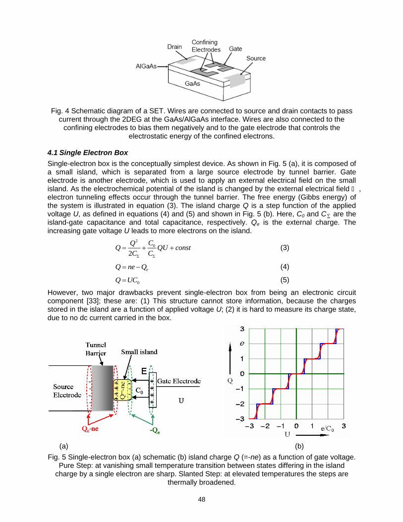
48
Fig. 4 Schematic diagram of a SET. Wires are connected to source and drain contacts to pass current through the 2DEG at the GaAs/AlGaAs interface. Wires are also connected to the
confining electrodes to bias them negatively and to the gate electrode that controls the electrostatic energy of the confined electrons.
4.1 Single Electron Box
Single-electron box is the conceptually simplest device. As shown in Fig. 5 (a), it is composed of a small island, which is separated from a large source electrode by tunnel barrier. Gate electrode is another electrode, which is used to apply an external electrical field on the small island. As the electrochemical potential of the island is changed by the external electrical field , electron tunneling effects occur through the tunnel barrier. The free energy (Gibbs energy) of the system is illustrated in equation (3). The island charge Q is a step function of the applied voltage U, as defined in equations (4) and (5) and shown in Fig. 5 (b). Here, C0 and C∑ are the island-gate capacitance and total capacitance, respectively. Qe is the external charge. The increasing gate voltage U leads to more electrons on the island.
2
0
2
CQQ QU const
C C
(3)
eQ ne Q (4)
0Q UC (5)
However, two major drawbacks prevent single-electron box from being an electronic circuit component [33]; these are: (1) This structure cannot store information, because the charges stored in the island are a function of applied voltage U; (2) it is hard to measure its charge state, due to no dc current carried in the box.
(a) (b)
Fig. 5 Single-electron box (a) schematic (b) island charge Q (=-ne) as a function of gate voltage. Pure Step: at vanishing small temperature transition between states differing in the island
charge by a single electron are sharp. Slanted Step: at elevated temperatures the steps are thermally broadened.

49
4.2 Single Electron Transistor
4.2.1 Coulomb blockade
The schematic of the single electron transistor with biased voltages is shown in Fig. 6. At first, it is assumed that the gate voltage, Vg is zero. If the biased voltage, Vb is less than the threshold voltage Vc (=e/CΣ), no electron can tunnel through the two tunnel junctions, because there is not sufficient energy to charge the island and hence tunneling rate is very low at low enough temperatures (kBT << Ec). This behavior is called Coulomb blockade [34]. When Vb is greater than Vc, the Coulomb blockade is overcome and current will flow through the circuit almost linearly as Vb is increases further as shown in Fig. 7 (a). The charge q contained in the whole island is given by equation (6).
1 2 0 0q q q q ne q (6)
where q0 is the background charge, which is non-integer and resulted from impurity, and e is the electron charge.
Fig. 6 Schematic of single-electron transistor circuit
Fig. 7 I-V curve of SET (a) zero Vg (b) changed Vg
4.2.2 Coulomb oscillation
Now it is assumed that Vg is not zero. The charges in the whole island are modified by the gate voltage Vg as given in equation (7).
0 2g gq ne q C V V (7)
The regions where current flowing through increase at the cost of the remaining Coulomb blockade region, therefore, increasing the bias voltage will increase the line-width of the oscillations. Besides, thermal broadening at higher temperature or a discrete energy spectrum also considerably changes the form of oscillations.
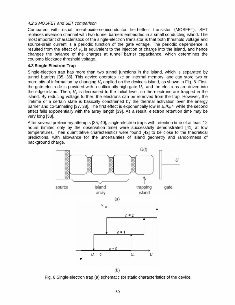
50
4.2.3 MOSFET and SET comparison
Compared with usual metal-oxide-semiconductor field-effect transistor (MOSFET), SET replaces inversion channel with two tunnel barriers embedded in a small conducting island. The most important characteristics of the single-electron transistor is that both threshold voltage and source-drain current is a periodic function of the gate voltage. The periodic dependence is resulted from the effect of Vg is equivalent to the injection of charge into the island, and hence changes the balance of the charges at tunnel barrier capacitance, which determines the coulomb blockade threshold voltage.
4.3 Single Electron Trap
Single-electron trap has more than two tunnel junctions in the island, which is separated by tunnel barriers [35, 36]. This device operates like an internal memory, and can store two or more bits of information by changing Vg applied on the device’s island, as shown in Fig. 8. First, the gate electrode is provided with a sufficiently high gate U+, and the electrons are driven into the edge island. Then, Vg is decreased to the initial level, so the electrons are trapped in the island. By reducing voltage further, the electrons can be removed from the trap. However, the lifetime of a certain state is basically constrained by the thermal activation over the energy barrier and co-tunneling [37, 38]. The first effect is exponentially low in Ec/kBT, while the second effect falls exponentially with the array length [39]. As a result, electron retention time may be very long [38].
After several preliminary attempts [35, 40], single-electron traps with retention time of at least 12 hours (limited only by the observation time) were successfully demonstrated [41] at low temperatures. Their quantitative characteristics were found [42] to be close to the theoretical predictions, with allowance for the uncertainties of island geometry and randomness of background charge.
Fig. 8 Single-electron trap (a) schematic (b) static characteristics of the device
51
5. ADVANTAGES AND SHORTCOMINGS
The major advantages of single electronics are: (i) Easy scalability which results from the operation of devices on Coulomb repulsion between electrons allowing the devices to operate at atomic dimensions rendering ultra-large scale integration possible, (ii) Low power dissipation because of the involvement of a very small number of electrons to accomplish basic operations, and (ii) High operating speed because of transference of a small number of electrons in a process contrary to the changing or discharging of a large number of electrons ~105 in a single digital operation.
The foremost difficulty encountered when using single-electron devices in a logic functional unit si their poor current drive capability as compared to CMOS devices. Since communication with a distantly located logic unit is prime requirement, this task is performed by CMOS devices. The second serious shortcoming is the need for low temperature operation. Such operation may be suitable for understanding the physical mechanisms of devices but the impact of the technology on industry and society will be felt only when the devices are capable of operating at room temperature, a feature which requires sub-10 nm structures that are not easy to fabricate from the lithographic standpoint. Thirdly, tunneling is exponentially sensitive to atomic layer fluctuations in barriers producing unacceptably large device to device variations.
Like the CMOS circuits, research in single-electron devices has also tended to pursue binary logic [43-45]. Methods used for single electron device research are direct electron beam writing and scanning probe manipulation. Low speed prevents the application of these methods to whole chip or whole wafer level. Consequently the fabrication of ULSI circuits with nm resolution seems a prohibitively costly affair. The prospects of single electronics, at least for computer logic, are therefore, discouraging [4]. Furthermore, it must be emphasized that present day technological problems like long interconnect delay and large power consumption can not be satisfactorily solved by simply replacing the conventional devices with the single electron ones. By this one-to-one substitution, the situation may even get worsened because of the low drivability resulting from the high tunneling resistance of single electron devices. The inferior drive capability of a single electron device leads to its poor interaction with a remotely located logic unit. This problem is circumvented by using a multi-valued logic scheme [46] that achieves high functionality with fewer components and interconnections [47] such as, periodic increase and decrease of drain current with gate voltage besides staircase-like increase of drain current with drain voltage thus providing more functions by using a smaller number of circuit components.
But single electronics/FET hybrid memory is promising [48-51]. Here, also the requirement of high cost ULSI nano fabrication methods such as, multiple electron beam writing is a major economic disadvantage. Besides, single electronics also provides the physical understanding of the limitations of single electron charging effects on nano scale devices. It has applications in unique scientific instrumentation like metrology or as tools of scientific research and for fundamental standards of current, resistance and temperature.
6. APPLICATIONS
The major applications of single electron transistors are: (i) Quantum processors that could be used to make several orders of faster PCs than the present day super computers, (ii) Solid state ultra dense memories, (iii) Logic devices, such as, AND, OR, XOR etc. gates, (iv) Quantum cellular automation (QCA), (v) Microwave signal detection, (vi) High sensitivity electrometer, (vii) Bio-sensing and environmental monitoring, (viii) Smart sensors, (ix) Super conductors, (x) Artificial atoms, (xi) Advanced electronic materials, (xii) Ultra high frequency (terahertz) and infra red radiation detection, (xiii) Metrology, (xiv) Imaging, (xv) DC current standards, (xvi) Temperature standards etc.
52
7. CONCLUSION
This paper reviews the history, the basic understanding of the theory of operation, advantages and disadvantages as well as few application areas of the single electron transistors. Since the CMOS technology is trending into sub-10 nm regime, single electron transistor or its hybrid may support the CMOS based integrated circuits. Because the transistors are oxide-based, they possess a ferroelectric property that allows them to act as solid-state memory. That means that even when they are powered down they can control the number of electrons on the island. The number of electrons dictates the ones and zeros that are the basis of computer memory, meaning that a future computer based on such transistors could hold its data even without external power. Therefore, his technology may be the component of future super-faster computing and memory devices. Even it might be competitive to single photon transistor i.e., optical quantum computing.
REFERENCES
[1] J. P. Colinge and C. A. Colinge, “Physics of semiconductor Devices,” Kluwer Academic Publishers, New York, USA, 2002.
[2] International Technology Roadmap for Semiconductors (ITRS), 2010 Executive Summery, http://www.itrs.net/, retrieved on 21 July 2011.
[3] http://www.webopedia.com/TERM/S/single_electron_transistor.html, Retrieved: 21st May 2012.
[4] K. Likharev, “Single-electron devices and their applications”, Proc. IEEE, vol. 87, pp.606-632, April 1999.
[5] C. Wasshuber, “Single-electronics–How it works. How it’s Used. How it’s simulated,” Proc. ISQED’02, 2002.
[6] H. R. Zeller, and I. Giaver, Phys. Rev. vol. 181, 1969, p. 789.
[7] K. K. Likharev, IBM J. Res. Device, vol. 32, 1988, p. 144.
[8] D. V. Averin and K. K. Likharev, “Mesoscopic Phenomena in Solids,” edited by B.L. Altshuler, P. A. Lee and R. A. Webb, Elsevier, Amsterdam, 1991.
[9] M. Amman, K. Mullen and E. Ben-Jacob, J. Appl. Physics, vol. 65, 1989, p. 339.
[10] L. I. Glazman and R. I. Shekhter, J. Phys. Condensed Matter, vol. 1, 1989, p. 5811.
[11] I. O. Kulik and R. I. Shekhter, "Kinetic phenomena and charge discreteness effects in granular media," Zh. Eksp. Teor. Fiz. vol. 68, 1975, p. 623.
[12] C.J. Gorter, "A possible explanation of the increase of the electric resistance of thin metal films at low temperatures and small field strength," Physical, vol. 15, pp. 777-780, August 1951.
[13] C.A. Neugebauer and M.B. Webb, "Electrical conduction mechanism in ultra thin, evaporated metal films," J. Appl. Phys., vol. 33, pp. 74-82, January 1962.
[14] H.R. Zeller and I. Giaever, "Tunneling, zero-bias anomalies, and small superconductors," Phys. Rev., vol. 181, pp. 789-799, May 1969.
[15] J. Lambe and R.C. Jaklevic, "Charge-quantization studies using tunnel capacitor," Phys. Rev. Lett., vol. 22, pp. 1371-1375, June 1969.
[16] I.O. Kulik and R.I. Shekhter, "Kinetic phenomena and charge discreteness effects in granular media," Zh. Eksp. Teor. Fiz. vol. 62, pp. 623-640 [Sov. Phys. - JETP, vol. 41, pp. 308-316], February 1975.
[17] K.K. Likharev, "Correlated discrete transfer of single electrons in ultra small tunnel junctions," IBM J. Res. Devel., vol. 32, pp. 144-158, January 1988.
[18] D.V. Averin and K.K. Likharev, "Single-electronics: Correlated transfer of single electrons and Copper pairs in small tunnel junctions," in Mesoscopic Phenomena in Solids, ed. by B. Altshuler, P. Lee and R. Webb. Amsterdam: Elsevier, 1991, p. 173-271.
[19] Single Charge Tunneling, ed. by H. Grabert and M.H. Devoret. New York: Plenum, 1992.
[20] T.A. Fulton and G.D. Dolan, "Observation of single-electron charging effects in small tunnel junctions", Phys. Rev. Lett., vol. 59, pp. 109-112, July 1987.
53
[21] J. H. F. Scott-Thomas, S. B. Field, M. A. Kastner, H. I. Smith, and D. A. Antoniadis, Phys. Rev. Letter, vol. 62, 1989, p. 583.
[22] U. Meirav, M.A. Kastner, and S.J. Wind, Phys. Rev. Letter, vol. 65, 1990, p. 771.
[23] A.T. Johnson, L.P. Kouwenhoven, W. de Jong, N.C. van der Vaart, C.J.P.M. Harmans, and C.T. Foxon, Phys. Rev. Letter, vol. 69, 1992, p. 1592.
[24] E. B. Foxman, P. L. McEuen, U. Meirav, N. S. Wingreen, Y. Meir, P. A. Belk, N. R. Belk, M. A. Kastner, and S. J. Wind, Phys. Rev. vol. B 47, 1993, p. 1020.
[25] J. Weis, R.J. Haug, K. v. Klitzing, and K. Ploog, Phys. Rev. Letter, vol. 71, 1993, p. 4019.
[26] A. M. Chang, H. U. Baranger, L. N. Pfeiffer, K. W. West, and T. Y. Chang, Phys. Rev. Letter, vol. 76, 1996, p. 1695.
[27] D. B. Chklovskii, BI. Shklovskii, and L. I. Glazman, Phys. Rev. vol. B 46, 1992, 4026.
[28] O. Klein, C. de C. Chamon, D. Tang, D.M. Abusch-Magder, S.-G. Wen, M.A. Kastner and S.J. Wind, Phys. Rev. Letter vol. 74, 1994, p. 785.
[29] C. B. Murray, D. J. Norris, M. G. Bawendi, J. Am. Chem. Soc. vol. 115, 1993, p. 8706.
[30] Y. Takahashi, M. Nagase, H. Namatsu, K. Kurihara, K. Iwdate, Y. Nakajima, S. Horiguchi, K. Murase, and M. Tabe, Electronics Letters, vol. 31, 1995, p. 136.
[31] C. Wasshuber, “Single-electronics–How it works. How it’s Used. How it’s simulated,” Proc. ISQED’02, 2002.
[32] K.K. Likharev, N.S. Bakhvalov, G.S. Kazacha, and S.I. Serdyukova, "Single-Electron Tunnel Junction Array: An Electrostatic Analog of the Josephson Transmission Line", IEEE Trans. Magn., vol. 25, pp. 1436-1439, March 1989.
[33] Y. Nakamura, C.D. Chen, and J.S. Tsai, “100-K operation of Al-based single-electron transistors,” Jpn. J. Appl. Phys., vol.35, pt.2, pp.L1465-1467, Nov. 1996.
[34] D.V. Averin and K.K. Likharev, "Coulomb blockade of tunneling, and coherent oscillations in small tunnel junctions", J. Low Temp. Phys., vol. 62, pp. 345-372, February 1986.
[35] T. A. Fulton, P.L Gammel, and L. N. Dunkleberger, “Determination of Coulomb-blockade resistances and observation of the tunneling of single electrons in small-tunnel-junction circuit,” Phys. Rev. Lett. Vol. 67, pp. 3148-3151, Nov. 1991.
[36] D. V. Averin and K. K. Likharev, “Possible applications of the single charge tunneling, in Single charge tunneling,” ed. By H. Grabert and M. H. Devoret. New York: Plenum, 1002, pp. 311-322.
[37] D.V. Averin and A.A. Odintsov, "Macroscopic quantum tunneling of the electric charge in small tunnel junctions," Phys. Lett. A, vol. 140, pp. 251-257, September 1989.
[38] L.R.C. Fonseca, A.N. Korotkov, K.K. Likharev, and A.A Odintsov, "Numerical Study of the Dynamics and Statistics of Single Electron Systems," J. Appl. Phys., vol. 78, pp. 3238-9125, September 1995.
[39] D. Porath and O. Millo, "Single electron tunneling and level spectroscopy of isolated C60 molecules," J. Appl. Phys., vol. 81, pp. 2241-2244, March 1997; D. Porath, Y. Levi, M. Tarabiah, and O. Millo, "Tunneling spectroscopy of isolated C60 molecules in the presence of charging effects," Phys. Rev. B, vol. 56, pp. 9829-9833, October 1997.
[40] P. Lafarge, P. Joyez, H. Pothier, A. Cleland, T. Holst, D. Esteve, C. Urbina, and M. Devoret, "Observation directe de la quantification de la charge macroscopique", C.R. Acad. Sci. Paris, vol. 314, pp. 883-888, April 1992.
[41] P. Dresselhaus, J. Li, S. Han, L. Ji, J.E. Lukens, and K.K. Likharev, "Measurement of single electron lifetimes in a multijunction trap", Phys. Rev. Lett., vol. 72, pp. 3226-3229, May 1994; L. Ji, P.D. Dresselhaus, S. Han, K. Lin, W. Zheng, and J. Lukens, "Fabrication and characterization of single-electron transistors and traps", J. Vac. Sci. Technol. B, vol. 12, pp. 3619-3622, November-December 1994.
[42] K.A. Matsuoka, K.K. Likharev, P. Dresselhaus, L. Ji, S. Han, and J. Lukens, "Single electron traps: A quantitative comparison of theory and experiment", J. Appl. Phys., vol. 81, pp. 2269-2281, March 1997.
52 (i)
54
[43] J. R. Tucker, "Complimentary digital logic based on the Coulomb blockade," Journal of Applied Physics, vol. 72, pp. 4399-4413, 1992.
[44] Y. Takahashi et al, "Multistage single electron transistors and their application to an exclusive OR gate," Appl. Phys. Lett. vol. 76, pp. 637-639, 2000.
[45] Y. Ono et al, "Complimentary single electron inverter with voltage gain,” Appl. Phys. Lett. vol. 76, pp. 3121-3123, 2000.
[46] H. Inokawa, A. Fujiwar and Y. Takahashi, "A multi-valued logic and memory combined single electron and metal oxide semiconductor transistors," IEEE Trans. Electron Dev. vol. 50, pp. 462-470, 2003.
[47] H. Inokawa and Y. Takahashi, "A compact analytical model for asymmetric single electron tunneling transistors," IEEE Trans. Electron Dev. vol. 50, pp. 455-461, 2003.
[48] H. Inokawa, A. Fujiwara, and Y. Takahashi, "A merged single-electron transistor and metal\–oxide\–semiconductor transistor logic for interface and multiple-valued functions," Jpn. J. Appl. Phys., vol. 41, pp.2566 -2568, 2002.
[49] Bong-Hoon Lee, "A novel SET/MOSFET hybrid static memory cell design," IEEE Transactions on Nanotechnology, Volume: 3, Issue: 3, pp. 377-382, Sept. 2004.
[50] S.J. KIM et al, "Single-Electron Logic Cells and SET/FET Hybrid Integrated Circuits," Journal of Semiconductor Technology and Science, Vol. 6, No.1, pp. 52-58, March, 2006.
[51] A. M. Ionescu, M. J. Declercq, S. Mahapatra, K. Banerjee and J. Gautier, “Few electron devices: towards hybrid CMOS-SET integrated circuits,” Proceedings of the 39
th Annual Design Automation
Conference, pp. 88-93, 2002.
52 (ii)

53
J. Bangladesh Electron. 14 (1-2); 53-57, 2014
Efficiency and Effectiveness of Associative Random Access
Memory in Solving Difficult Tasks
Dr. Md. Abdul Malek and Md. Mohibullah *Department of Computer Science and Engineering,
*Comilla University, Comilla, Bangladesh
[email protected], [email protected], [email protected]
Abstract
In this paper, we have proposed an efficient system to recognize symbols (e.g., letters, words, images, gestures etc.) in an associative environment. For instance, we have taken the system to recognize the letters in the Russian Alphabet. This paper represents a method of formation and recognition of codes for the letters in a seven segment elements of matrixes in the associative cells of the Associative Random Access Memory (ARAM). For the recognition of codes of letters in the associative environment, the algorithm is developed throughout the paper.
Keywords: Recognition of symbol, associative environment, algorithm.
1. INTRODUCTION
Associative memory is a special type of computer memory. In associative memory, storage locations are accessed by their contents of data or the parts of contents, not by the position. Generally, it is used to search the applications which are needed to search with very high speed. It is also known as Content Addressable Memory (CAM).
In this world, most of the works, related to the computer memories, are done using the classical memories. Some works are based on associative memories. Because of the associative memories are more expensive than the classical memories. Although associative memories are expensive but they are highly applicable when we need to search something with very high speed. As their fast processing time, we have selected our work-the recognition of symbols in the associative environment.
The concept of symbols in matrixes ARAM is based on the following: any symbol of the Russian alphabet is represented with a set of the associated vertical and horizontal pieces of lines and a diagonal direction with a slope 450 and 1350.
For recognition it is supposed to place the symbol in matrix ARAM by following rules:
1. The image of a symbol begins with an extreme left column (Щ, Ш, Н, Г, Ц, Е, Ы, П, Р, Ч, M, Ь,) and extreme top line (Г, П, A, B, Л, Т, Б) of matrixes ARAM. Symbols Л and Д will not start from the left top element of a matrix (Fig. 1- 4).
2. Across on a horizontal and on a vertical contour symbol uses 1 bit that is, thickness is considered to a contour of a symbol individual.
3. Codes of adjacent horizontal or vertical parallel pieces of symbols (for example, vertical pieces in letters И, Н, Ш, Щ, П, А) settle down accordingly in lines or columns, from each other for one line or one column, that is, between parallel pieces there are codes of space -«Zero» codes.
4. Proceeding from item 1-3, for coding all letters of the Russian alphabet 5 lines of matrix ARAM are required. Quantity of columns is required from 3 for maximum letters and up to 6 for the letter Щ.
5. Diagonal lines of symbols should not have less than three elements of a matrix adjacent on a diagonal with one value. For example, the code of the letter M requires 5х5 elements of a matrix and a code of a direct diagonal is equal to 11101, the code of a return diagonal is equal to 10111.

54
6. At coding vertical pieces of the symbols engaging an incomplete column, e. g., for symbols Б, Ч, Ф, Р, У, Ь, Ы, Я, necessary three bits, accepting value «1».
7. Feature of coding of symbols Э and З is that codes of middle lines differ one bit: for symbol Э - code 011, for symbol З- code 111.
2. ALGORITHM FOR FORMATION OF CODES
The algorithm for formation of codes of library of pieces of the symbols which are stored in the associative storage and being in essence by codes of signs of symbols is based on following preconditions:
1. The code of a symbol engages a matrix 5х6 (5 lines, 6 columns).
2. «1» values of elements of a matrix form shape of a symbol.
The essence of algorithm for formation of codes of the symbols forming library of codes of samples of symbols, consists in the following:
Step 1:
1. On the register of interrogation of the block of register RA [BR1] [1, 3] and the register of interrogation of the block of register RA [BR2], codes 111111 and 11111 move at the same time.
2. Check of these codes on concurrence to codes accordingly all 5 lines and all 6 columns of letters of the alphabet is carried out and the result is recorded in appropriating categories of registers of fixing RS1 and RS2.
3. Received in RS1 and RS2 the pair codes forms the first code of a sign of the given letter which is recorded in the first section of a matrix of library of samples.
Step 2:
1. Place the code 111mmm on RA [BR1] and the code mm101 on RA [BR2], where m is the disguised category which is not participating in check on concurrence of codes.
2. Fulfilling the check on concurrence of these codes to codes of letters of the alphabet accordingly all 5 lines and all 6 columns of letters of the alphabet and the result is recorded in appropriating categories of registers of fixing RS1 and RS2.
3. Received in RS1 and RS2, the second pair codes form the second code of a sign of the given letter which is recorded in the second section of a matrix of library of samples.
Step 3:
The received two pair’s codes are kept in memory of library of codes of samples (signs) of letters. Thus, memory of library of codes will consist of two parts on 11 categories, that is, a full code of signs depending on the letter 11 bits (for letters of M, Т, X, Щ) or 22 bits (for the others).
3. ALGORITHM FOR RECOGNITION OF CODES
The algorithm for recognition of codes of letters in the associative environment consists in the following:
1. Place the code of the unknown letter in memory ARAM.
2. Place the codes 111111 and 11111 on the register of interrogation of the block of register RA [BR1] and the register of interrogation of the block of register RA [BR2] respectively at the same time.
2.1. Checking of these codes on concurrence of codes accordingly all 5 lines and all 6 columns of a code of the unknown letter is carried out and the result is recorded in appropriating categories of registers of fixing RS1 and RS2.
2.2. Received in RS1 and RS2, the pair of codes forms the first code of a sign of the given letter.
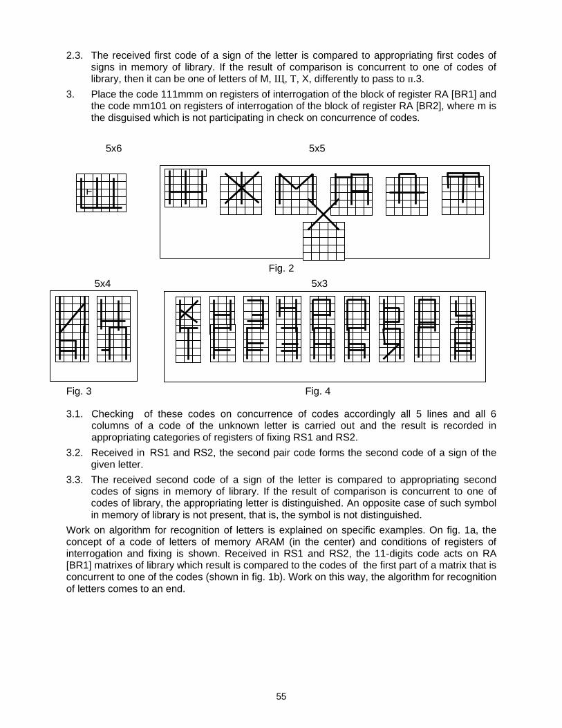
55
2.3. The received first code of a sign of the letter is compared to appropriating first codes of signs in memory of library. If the result of comparison is concurrent to one of codes of library, then it can be one of letters of M, Щ, Т, X, differently to pass to п.3.
3. Place the code 111mmm on registers of interrogation of the block of register RA [BR1] and the code mm101 on registers of interrogation of the block of register RA [BR2], where m is the disguised which is not participating in check on concurrence of codes.
5x6 5x5
Fig. 1
Fig. 2
5x4 5x3
Fig. 3 Fig. 4
3.1. Checking of these codes on concurrence of codes accordingly all 5 lines and all 6 columns of a code of the unknown letter is carried out and the result is recorded in appropriating categories of registers of fixing RS1 and RS2.
3.2. Received in RS1 and RS2, the second pair code forms the second code of a sign of the given letter.
3.3. The received second code of a sign of the letter is compared to appropriating second codes of signs in memory of library. If the result of comparison is concurrent to one of codes of library, the appropriating letter is distinguished. An opposite case of such symbol in memory of library is not present, that is, the symbol is not distinguished.
Work on algorithm for recognition of letters is explained on specific examples. On fig. 1a, the concept of a code of letters of memory ARAM (in the center) and conditions of registers of interrogation and fixing is shown. Received in RS1 and RS2, the 11-digits code acts on RA [BR1] matrixes of library which result is compared to the codes of the first part of a matrix that is concurrent to one of the codes (shown in fig. 1b). Work on this way, the algorithm for recognition of letters comes to an end.
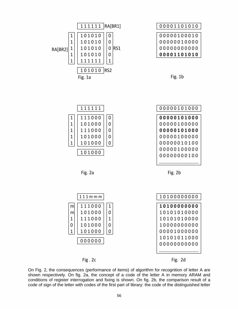
56
1 1 1 1 1 1
1 0 1 0 1 01 0 1 0 1 01 0 1 0 1 01 0 1 0 1 01 1 1 1 1 1
00001
11111
1 0 1 0 1 0
0 0 0 0 1 1 0 1 0 1 0
0 0 0 0 0 1 0 0 0 1 00 0 0 0 0 0 1 0 0 0 00 0 0 0 0 0 0 0 0 0 00 0 0 0 1 1 0 1 0 1 0
1 1 1 1 1 1
1 1 1 0 0 01 0 1 0 0 01 1 1 0 0 01 0 1 0 0 01 0 1 0 0 0
00000
11111
1 0 1 0 0 0
0 0 0 0 0 1 0 1 0 0 0
0 0 0 0 0 1 0 1 0 0 00 0 0 0 0 1 0 0 0 0 00 0 0 0 0 1 0 1 0 0 00 0 0 0 0 1 0 0 0 0 00 0 0 0 0 0 1 0 1 0 00 0 0 0 0 1 0 0 0 0 00 0 0 0 0 0 0 0 1 0 0……………………………..
1 1 1 m m m
1 1 1 0 0 01 0 1 0 0 01 1 1 0 0 01 0 1 0 0 01 0 1 0 0 0
10100
0 0 0 0 0 0
mm101
Fig. 1a Fig. 1b
Fig. 2a Fig. 2b
Fig . 2c
1 0 1 0 0 0 0 0 0 0 0
1 0 1 0 0 0 0 0 0 0 01 0 1 0 1 0 1 0 0 0 01 0 1 0 1 0 1 0 0 0 01 0 0 0 0 0 0 0 0 0 00 0 0 0 1 0 0 0 0 0 01 0 1 0 1 0 1 1 0 0 00 0 0 0 0 0 0 0 0 0 0……………………………..
Fig. 2d
RA[BR1]
RA[BR2] RS1
RS2
On Fig. 2, the consequences (performance of items) of algorithm for recognition of letter A are shown respectively. On fig. 2a, the concept of a code of the letter A in memory ARAM and conditions of register interrogation and fixing is shown. On fig. 2b, the comparison result of a code of sign of the letter with codes of the first part of library: the code of the distinguished letter

57
has coincided with codes of the letter A and B, therefore the algorithm passes to item 3 according to which the second code of a sign of the letter (condition RA [BR1] and RA [BR2] is shown in fig. 2c), which is compared to codes of the second part of library (shown in fig. 2d). Thus, the result of comparison is concurrent to codes of signs of the letter A.
4. CONCLUSION
It is very easy to recognize images, words or gestures including the letters of the Russian Alphabet in an associative environment. Also these symbols can be easily processed. That is, the processing time in an associative memory is relatively low. So the memory is not wasted much because of the participation of CPU need not be longer to process a letter, a word or an image. In this paper, our objective was how to recognize a symbol in the associative cells of the Associative Random Access Memory (ARAM). Here we have considered the letters of the Russian Alphabet as an instance. In future, we will work on how one can see the visual effect of symbol recognition by comparing between the classical memories and the associative memories. That is, we will see the associative memories are faster than the classical memories to recognize the symbols. We have already started our work and we will continue until the ultimate result.
REFERENCES
[1] Ognev I. V., Boriss V. V. Intellectual systems of associative memory. М.: Radio and Svyaz, 1996.-176c.: silt.
[2] Ognev I. V., Boriss V. V. Associative environment. М.: Radio and Svyaz, 2000.-312 with.
[3] Ognev I. V., Md. Abdul Malek, processing of matrixes in the associative environment. International forum of information-2000: Reports of the international conference « Information means and technologies ». 17-19 October 2000г. In 3 vol. Т.2.-М: publishing house “Stankin", 2000г...-245 with

59
J. Bangladesh Electron. 14 (1-2); 59-64, 2014
Optical and Electrical Properties of One-dimensional Si NWs
Array Prepared by Electroless Metal Deposition (EMD)
Md. Ali Asgar1*, Md. Mahmudul Hasan1 and Zahid Hasan Mahmood2
1Department of Electronics and Communication Engineering, Jatiya Kabi Kazi Nazrul
Islam University, Trishal, Mymensingh, Bangladesh 2Department of Applied Physics Electronics and Communication Engineering
University of Dhaka, Dhaka – 1000, Bangladesh *E-mail: [email protected]
Abstract
The optical and electrical properties of one-dimensional (1D) silicon nanowires (Si NWs) array synthesized on clean silicon substrate by solution based chemical etching have been demonstrated. It has been found that Si NWs film shows very low optical reflection from the front surface and strong broadband optical absorption in the wavelength range of 200 nm to 900 nm compared to bulk silicon. The reported optical reflection measurement for type A sample is less than 1.2% in 200 nm to 450 nm wavelength range and it is around 2% over 200 nm to 820 nm wavelength range. The absorption of Si NWs array is about 78% for type A sample and 75% for type B sample whereas bulk Si absorbs only 46% of incident radiation. Thereafter, electrical current-voltage (I-V) measurement has been carried out by making aluminium contact to the synthesized samples and found to be higher than pure silicon. Those observed behaviors are effectively makes Si NW an important candidate for optoelectronic applications.
Keywords: Electroless Metal Deposition (EMD), Silicon Nanowires (Si NWs), Absorption, Reflection, Rectifying contact.
1. INTRODUCTION
To date nanotechnology is an exciting and rapidly growing area of research that spans the wide scope of interrelated fields from electronics, optoelectronics and energy to healthcare [1] [2]. Silicon (Si) is an important semiconducting material in microelectronic industry owing to their technological compatibility. Bulk silicon cannot emit visible light because it is an indirect bandgap material [3]. But low dimensional nanostructured Si such as silicon nanotubes (Si NTs) [4], silicon nano-cones (Si NCs) [5], porous silicon [6] and silicon nanowires (Si NWs) [7] can emit visible light as being direct bandgap materials [8]. For this reason, much effort has been invested in fabricating these low-dimensional nanostructured Si and their potential application in different microelectronic industries, for instance, Field-Effect Transistors (FETs) [9], inverters [10], photovoltaics and photodetectors [11], nanosensors [12], Light-Emitting Diodes (LEDs) and laser [13], decoder [14], nonvolatile memory, programmable logic [15] and silicon nano-anodes in practical lithium batteries [16] etc.
Among other nanostructures, one dimensional free standing silicon nanowires (Si NWs) have grabbed special interest because of their unique electrical, optical properties and thermal properties. In addition to that, Si NWs are completely semiconducting in nature compared to carbon nanotube (CNT) which can be metallic as well as semiconducting depending on growth condition [17]. Therefore, much interest has been made to prepare Si NWs by numerous methods such as Vapor-Liquid-Solid (VLS) mechanism, Chemical Vapor Deposition (CVD), Electron Beam Lithography (EBL), Molecular Beam Lithography (MBE), Laser Ablation, supercritical fluid liquid solid (SFLS) synthesis and other methods [18]. These methods are quite accessible and well controlled.
In Si microelectronic technology, synthesis of Si NWs by electrolytic process has spurred concentrated research activity. Particularly, Si shows a complex electrochemical etching

60
behavior in solution containing hydrofluoric acid. Electroless Metal Deposition (EMD) and Electroless etching behavior have been widely accepted because of their technical compatibility in fabricating various Si nanostructures. EMD method is often described as a galvanic displacement process that involves the spontaneous oxidation of Si atoms and the reduction of metal ions to metallic particles and films in the absence of an external source of electric current. The galvanic displacement process can be described using mixed potential theory.
In this article, we report electrical and optical measurement on silicon nanowires array synthesized by means of Electroless Metal Deposition (EMD) and solution based metal assisted chemical etching. This electrolytic process is capable of producing high aspect ratio silicon micro and nanostructure. Electroless Metal Deposition (EMD) technique was chosen for synthesis of silicon nanowire as it is feasible to implement using available facilities and necessary chemicals are available here in local chemical market of Dhaka, Bangladesh.
2. EXPERIMENTAL DETAILS
Silicon nanowires films were synthesized on solid silicon surface to measure both reflection and absorption. The whole procedure was conducted in a teflonlined vessel and consist of three steps: i) Cleaning the silicon substrates with cleaning solution— here we consecutively used acetone (5 min), ethanol (5 min), deionized water (2–3 times), and H2SO4/H2O2 (3:1 H2SO4 (97%)/H2O2 (30%), 10 min), then the wafers were thoroughly rinsed with deionized water (10 min) and dipped into a solution of HF (1 min); ii) Electroplating onto the cleaned Si surface by the metal-nanoparticle. A group of cleaned samples (sample type A) were dipped in HF/AgNO3
solution for silver (Ag) nanoparticle deposition. Deposition time was varied from 60s to 75s. The concentration of HF and AgNO3 were 5M and 0.02M respectively. Another group of samples (sample type B) were dipped in HF/ Cu(NO3)2.H2O for copper (Cu) nanoparticles deposition. In this case deposition time was varied from 60s to 120s. The concentration of HF was 5M but for Cu(NO3)2.H2O it was varied from 0.02M to 0.05M; iii) After deposition of silver/copper nanoparticles, the silver/copper covered substrate was immersed in an etching solution. The solution was HF based Fe(NO3)3, where the concentration of HF and Fe(NO3)3 were 5M and 0.02M respectively. Etching was performed at room temperature for 30min to 75min.This wet chemical etching mechanism allows the formation of silicon nanowires (Si NWs) film. The diameter of the individual nanowires was in the range of 45 nm to 200 nm and the length from 2 µm to 4 µm confirmed from scanning electron microscopy (SEM) investigation. The SEM micrograph of the Si NWs arrays is shown in Figure 1.
The obtained samples then characterized to perform optical and electrical study. The optical absorption and reflection measurement were obtained on a Shimadzu UV-1201 single beam absorption spectrophotometer. After optical investigation we performed electrical measurement by making a thin layer of aluminium (Al) film to the nanowires (NWs) synthesized samples on a thermal evaporator.
3. RESULT AND DISCUSSION
Silicon nanowire films fabricated by Metal Assisted Chemical Etching (MCE) process on clean silicon substrates were investigated to study the optical and electrical behavior. The optical characterization and electrical measurements are discussed in the following sections.
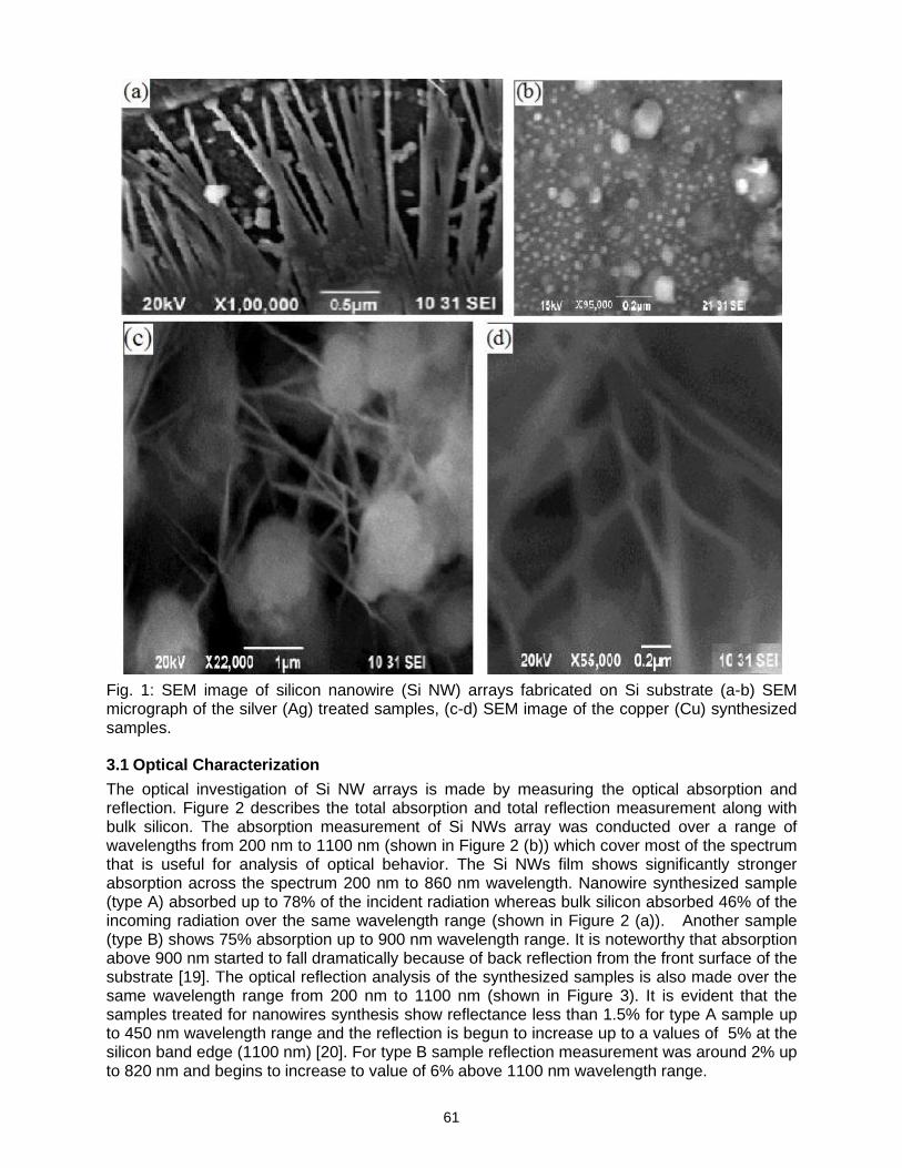
61
Fig. 1: SEM image of silicon nanowire (Si NW) arrays fabricated on Si substrate (a-b) SEM micrograph of the silver (Ag) treated samples, (c-d) SEM image of the copper (Cu) synthesized samples.
3.1 Optical Characterization
The optical investigation of Si NW arrays is made by measuring the optical absorption and reflection. Figure 2 describes the total absorption and total reflection measurement along with bulk silicon. The absorption measurement of Si NWs array was conducted over a range of wavelengths from 200 nm to 1100 nm (shown in Figure 2 (b)) which cover most of the spectrum that is useful for analysis of optical behavior. The Si NWs film shows significantly stronger absorption across the spectrum 200 nm to 860 nm wavelength. Nanowire synthesized sample (type A) absorbed up to 78% of the incident radiation whereas bulk silicon absorbed 46% of the incoming radiation over the same wavelength range (shown in Figure 2 (a)). Another sample (type B) shows 75% absorption up to 900 nm wavelength range. It is noteworthy that absorption above 900 nm started to fall dramatically because of back reflection from the front surface of the substrate [19]. The optical reflection analysis of the synthesized samples is also made over the same wavelength range from 200 nm to 1100 nm (shown in Figure 3). It is evident that the samples treated for nanowires synthesis show reflectance less than 1.5% for type A sample up to 450 nm wavelength range and the reflection is begun to increase up to a values of 5% at the silicon band edge (1100 nm) [20]. For type B sample reflection measurement was around 2% up to 820 nm and begins to increase to value of 6% above 1100 nm wavelength range.
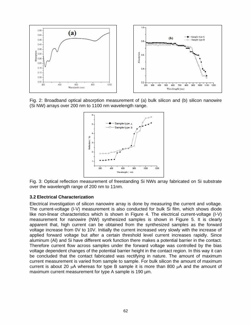
62
Fig. 2: Broadband optical absorption measurement of (a) bulk silicon and (b) silicon nanowire (Si NW) arrays over 200 nm to 1100 nm wavelength range.
Fig. 3: Optical reflection measurement of freestanding Si NWs array fabricated on Si substrate over the wavelength range of 200 nm to 11nm.
3.2 Electrical Characterization
Electrical investigation of silicon nanowire array is done by measuring the current and voltage. The current-voltage (I-V) measurement is also conducted for bulk Si film, which shows diode like non-linear characteristics which is shown in Figure 4. The electrical current-voltage (I-V) measurement for nanowire (NW) synthesized samples is shown in Figure 5. It is clearly apparent that, high current can be obtained from the synthesized samples as the forward voltage increase from 0V to 10V. Initially the current increased very slowly with the increase of applied forward voltage but after a certain threshold level current increases rapidly. Since aluminum (Al) and Si have different work function there makes a potential barrier in the contact. Therefore current flow across samples under the forward voltage was controlled by the bias voltage dependent changes of the potential barrier height in the contact region. In this way it can be concluded that the contact fabricated was rectifying in nature. The amount of maximum current measurement is varied from sample to sample. For bulk silicon the amount of maximum current is about 20 μA whereas for type B sample it is more than 800 μA and the amount of maximum current measurement for type A sample is 190 µm.
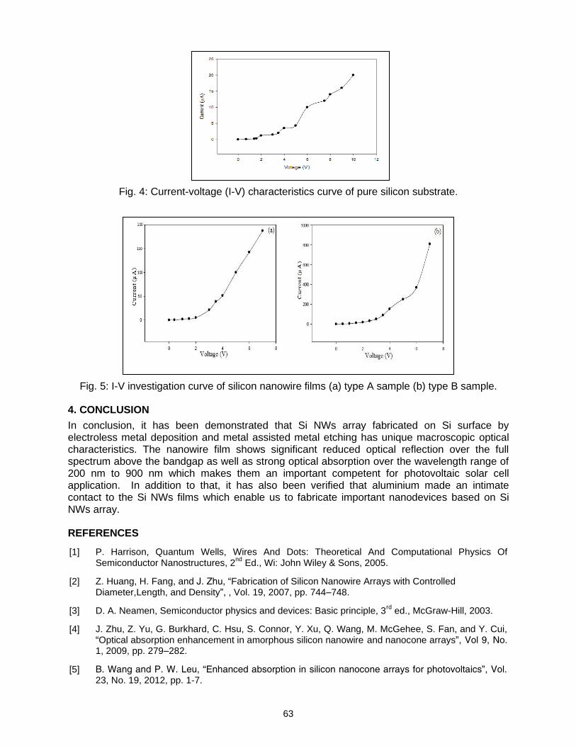
63
Fig. 4: Current-voltage (I-V) characteristics curve of pure silicon substrate.
Fig. 5: I-V investigation curve of silicon nanowire films (a) type A sample (b) type B sample.
4. CONCLUSION
In conclusion, it has been demonstrated that Si NWs array fabricated on Si surface by electroless metal deposition and metal assisted metal etching has unique macroscopic optical characteristics. The nanowire film shows significant reduced optical reflection over the full spectrum above the bandgap as well as strong optical absorption over the wavelength range of 200 nm to 900 nm which makes them an important competent for photovoltaic solar cell application. In addition to that, it has also been verified that aluminium made an intimate contact to the Si NWs films which enable us to fabricate important nanodevices based on Si NWs array.
REFERENCES
[1] P. Harrison, Quantum Wells, Wires And Dots: Theoretical And Computational Physics Of Semiconductor Nanostructures, 2
nd Ed., Wi: John Wiley & Sons, 2005.
[2] Z. Huang, H. Fang, and J. Zhu, “Fabrication of Silicon Nanowire Arrays with Controlled Diameter,Length, and Density”, , Vol. 19, 2007, pp. 744–748.
[3] D. A. Neamen, Semiconductor physics and devices: Basic principle, 3rd
ed., McGraw-Hill, 2003.
[4] J. Zhu, Z. Yu, G. Burkhard, C. Hsu, S. Connor, Y. Xu, Q. Wang, M. McGehee, S. Fan, and Y. Cui, “Optical absorption enhancement in amorphous silicon nanowire and nanocone arrays”, Vol 9, No. 1, 2009, pp. 279–282.
[5] B. Wang and P. W. Leu, “Enhanced absorption in silicon nanocone arrays for photovoltaics”, Vol. 23, No. 19, 2012, pp. 1-7.
64
[6] Y. Tang, L. Pei, Y. Chen, C. Guo, “Self-Assembled Silicon Nanotubes under Supercritically Hydrothermal Conditions”, Vol. 95, No. 11, 2005, pp. 1-4.
[7] H. Fang, X. Li, S. Song, Y. Xu, J. Zhu, “Fabrication of slantingly-aligned silicon nanowire arrays for solar cell applications”, Vol. 19, No. 25, 2008, pp. 1-5.
[8] Y. Zhen, C. Rivas, R. Lake, K. Alam and R. B. Boykin, “Electronic properties of Silicon Nanowires”, Vol. 52, No. 6, 2005, pp. 1097-1103.
[9] Y. Cui, Z. Zhong, D. Wang, W. U. Wang, and C. M. Lieber, “High performance silicon nanowire field effect transistors”, Vol. 3, No. 2, 2003 pp. 149–152.
[10] Y. Cui and C. M. Lieber, “Functional nanoscale electronic devices assembled using silicon nanowire building blocks”, Vol. 291, 2001, pp.851–853.
[11] J. F. Wang, M. S. Gudiksen, X. F. Duan, Y. Cui, and C. M. Lieber,“Highly polarized photoluminescence and photodetection from single indium phosphide nanowires”, Vol. 293, 2001, pp. 1455–1457.
[12] J. Hahm and C. M. Lieber, “Direct ultrasensitive electrical detection of dna and dna sequence variations using nanowire nanosensors”, Vol. 4, No. 1, 2004, pp. 51–54.
[13] X. Duan, Y. Huang, R. Agarwal, and C. M. Lieber, “Single-nanowire electrically driven lasers”, Vol. 421, 2003, pp. 241–245.
[14] Z. Zhong, D. Wang, Y. Cui, M. W. Bockrath, and C. M. Lieber, “Nanowire crossbar arrays as address decoders for integrated nanosystems”, Vol. 302, 2003, pp. 1377–9.
[15] Y. Huang, X. Duan, Y. Cui, L. J. Lauhon, K. H. Kim, and C. M. Lieber, “Logic gates and computation from assembled nanowire building blocks”, Vol. 294, 2001, pp. 1313–7.
[16] J. R. Szczech and S. Jin “Nanostructured silicon for high capacity lithium battery anodes”, Vol. 4, 2011, pp. 56-72.
[17] Y. Cui, X. Duan, J. Hu, and C. M. Lieber, “Doping and Electrical Transport in Silicon Nanowires”,Vol. 104, No. 22, 2000, pp. 5213-5216.
[18] P. R. Bandaru and P. Pichanusakorn, “An outline of the synthesis and properties of silicon nanowires”, Vol. 25, 2010, pp. 1-16.
[19] LoucasTsakalakos, Joleyn Balch, Jody Fronheiser, Min-Yi Shih, Steven F. LeBoeuf, Mathew Pietrzykowski, Peter J. Codella, Bas A. Korevaar, Oleg Sulima, Jim Rand, AnilkumarDavuluru, and UmakantRapol “Strong broadband optical absorption in silicon nanowire films”; Journal of Nanophotonics, Vol. 1, 013552; 2007
[20] X. Li, “Metal assisted chemical etching for high aspect ratio nanostructures: A review of characteristics and applications in photovoltaics”, Vol. 16, 2012, pp. 71-81.

65
J. Bangladesh Electron. 14 (1-2); 65-70, 2014
An Alternative Method for Decoding Hamming Codes Relying on
Maximum Likelihood Transmission Sequences
Saqib Shadman Bashar1 and Md Hossam-E-Haider2
1Department of Electrical and Electronic Engineering, University of Nottingham, Malaysia Campus
2Department of Electrical, Electronic and Communication Engineering
Military Institute of Science and Technology [email protected] and
Abstract
Block codes are one of the earliest classes of error correction codes. Over decades, powerful binary block codes have been developed. Different block codes have different ways of being decoded. The standard method of decoding a binary block code is to match syndrome vector weights with a lookup table. But practically, this would require too much time and processing power. In this paper, I propose an alternative method to decode hamming codes which should theoretically require less time and processing power.
Keywords: Hamming Code, Hamming Distance, Lookup Table.
1. INTRODUCTION
Forward error correction involves adding redundant bits to a certain information signal. Over noisy channels, information often tends to get corrupted during transmission. The redundant bits allow for the correction of errors. The number of errors that can be corrected depends on the number of redundant bits added to the signal. Generally, more bits added to the information signal allows for greater correction of errors.
The standard process for decoding binary block codes is described in [1]. For small codes such as the [7, 4] Hamming code, this should not pose any problems. However, for codes with larger error correction capabilities such as the [52,18,16] computational power and time required rises very high as the number of entries in the look up table is 6.893x10¹¹. To overcome this, a method has been proposed in which the Hamming distance between a received sequence and all possible entries in a much shorter lookup table is calculated. The entry with which the received sequence has least hamming distance was the entry originally sent on the transmission side.
For binary information transmission, the error involves bit- flips (i.e. a ‘1’ changes to a ‘0’and vice versa).
2. THE CODING PROCESS
A certain stream of bits is organized into a row vector. For example, if we have an input stream of the following sequence 101010101010101010
This sequence is arranged into a row vector, which is labeled as “Input”
Input = [1 0 1 0 1 0 1 0 1 0 1 0 1 0 1 0 1 0]
The coding process is quite simple for Hamming codes. If the generator matrix is G, the input string is denoted as x and the encoder output is y can be expressed as :
Gxy * (1)

66
For the [52,18,16] code, the generator matrix is defined in [2]. The codeword for the sequence “Input” is :
[1 0 1 0 1 0 1 0 1 0 1 0 1 0 1 0 1 0 1 1 1 0 0 1 1 0 0 0 0 0 1 0 1 1 0 0 1 0 1 0 0 1 0 0 0 1 0 1 0 1 0 1]
3. THE STANDARD DECODING PROCESS
A parity check matrix is constructed of which structure and elements depend on G. Syndrome vectors are calculated according to the following equation :
yHs * (2)
Where H represents the parity check matrix and s represents the syndrome vector. Hamming codes can at maximum correct 0.5(d-1) errors. In the case of the [52, 18, 16] block code, it can correct up to seven errors. A lookup table containing syndrome vectors of all possible error vectors and the corresponding hamming weights.
Suppose the sequence “Output” is sent through a noisy channel which introduces the error vector :
[1 0 0 0 0 0 0 0 0 0 0 1 0 0 0 0 0 0 0 1 0 0 0 0 0 0 0 0 0 0 0 0 0 0 0 0 0 1 0 0 0 0 0 0 0 0 0 0 0 0 0 1]
Suppose the sequence received on the receiving end is r. ‘r’ can be expressed as :
eyr (3)
The addition is a binary addition. Using Equation (3), the received sequence on the transmission end is :
[0 0 1 0 1 0 1 0 1 0 1 1 1 0 1 0 1 0 1 0 1 0 0 1 1 0 0 0 0 0 1 0 1 1 0 0 1 1 1 0 0 1 0 0 0 1 0 1 0 1 0 0]
The syndrome vector for the received sequence is :
[1 1 0 0 1 0 1 0 1 1 0 1 1 0 0 1 1 1 1 1 1 1 1 0 1 1 0 1 1 1 1 0 1 0]
Which corresponds to five errors. Therefore the error correction process contains five iteration stages. The iteration and correction processes are defined in [1].
4. VITERBI DECODER AND MAXIMUM LIKELIHOOD PATHS
Convolutional codes are implemented by using shift registers. Suppose we have a convolutional encoder with the following generator polynomials:
21
1
DDO (4)
2
2 1 DO (5)
Suppose we wish to encode the following binary sequence : 10010. Then, the output produced by the encoder defined by the polynomial equation (4) and equation (5) is : [0 1 1 0 1 1 0 1 1 0].
The sequence is sent through a Binary Symmetric Channel with error probability 0.2. The received sequence is 0110010010.
Now, we make use of the Viterbi decoder. The principle behind the Viterbi decoder is to simulate every path the encoder can take, produce the output for each path taken and compare the hamming distances between the simulated outputs and the received sequence to determine what the input sequence was.
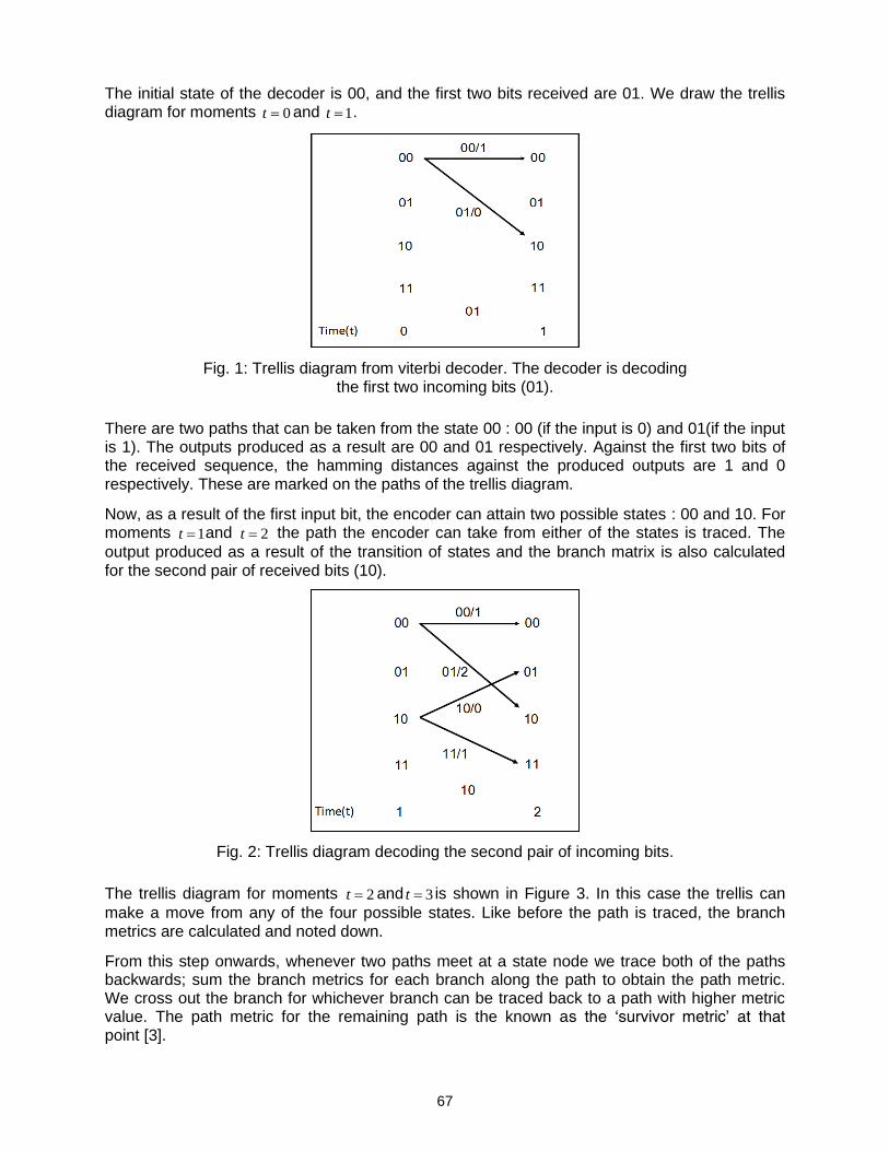
67
The initial state of the decoder is 00, and the first two bits received are 01. We draw the trellis diagram for moments 0t and 1t .
Fig. 1: Trellis diagram from viterbi decoder. The decoder is decoding the first two incoming bits (01).
There are two paths that can be taken from the state 00 : 00 (if the input is 0) and 01(if the input is 1). The outputs produced as a result are 00 and 01 respectively. Against the first two bits of the received sequence, the hamming distances against the produced outputs are 1 and 0 respectively. These are marked on the paths of the trellis diagram.
Now, as a result of the first input bit, the encoder can attain two possible states : 00 and 10. For moments 1t and 2t the path the encoder can take from either of the states is traced. The
output produced as a result of the transition of states and the branch matrix is also calculated for the second pair of received bits (10).
Fig. 2: Trellis diagram decoding the second pair of incoming bits.
The trellis diagram for moments 2t and 3t is shown in Figure 3. In this case the trellis can
make a move from any of the four possible states. Like before the path is traced, the branch metrics are calculated and noted down.
From this step onwards, whenever two paths meet at a state node we trace both of the paths backwards; sum the branch metrics for each branch along the path to obtain the path metric. We cross out the branch for whichever branch can be traced back to a path with higher metric value. The path metric for the remaining path is the known as the ‘survivor metric’ at that point [3].
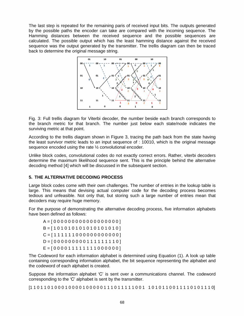
68
The last step is repeated for the remaining paris of received input bits. The outputs generated by the possible paths the encoder can take are compared with the incoming sequence. The Hamming distances between the received sequence and the possible sequences are calculated. The possible output which has the least hamming distance against the received sequence was the output generated by the transmitter. The trellis diagram can then be traced back to determine the original message string.
Fig. 3: Full trellis diagram for Viterbi decoder, the number beside each branch corresponds to the branch metric for that branch. The number just below each state/node indicates the surviving metric at that point.
According to the trellis diagram shown in Figure 3, tracing the path back from the state having the least survivor metric leads to an input sequence of : 10010, which is the original message sequence encoded using the rate ½ convolutional encoder.
Unlike block codes, convolutional codes do not exactly correct errors. Rather, viterbi decoders determine the maximum likelihood sequence sent. This is the principle behind the alternative decoding method [4] which will be discussed in the subsequent section.
5. THE ALTERNATIVE DECODING PROCESS
Large block codes come with their own challenges. The number of entries in the lookup table is large. This means that devising actual computer code for the decoding process becomes tedious and unfeasible. Not only that, but storing such a large number of entries mean that decoders may require huge memory.
For the purpose of demonstrating the alternative decoding process, five information alphabets have been defined as follows:
A = [ 0 0 0 0 0 0 0 0 0 0 0 0 0 0 0 0 0 0 ]
B = [ 1 0 1 0 1 0 1 0 1 0 1 0 1 0 1 0 1 0 ]
C = [ 1 1 1 1 1 1 0 0 0 0 0 0 0 0 0 0 0 0 ]
D = [ 0 0 0 0 0 0 0 0 0 1 1 1 1 1 1 1 1 0 ]
E = [ 0 0 0 0 1 1 1 1 1 1 1 1 0 0 0 0 0 0 ]
The Codeword for each information alphabet is determined using Equation (1). A look up table containing corresponding information alphabet, the bit sequence representing the alphabet and the codeword of each alphabet is created.
Suppose the information alphabet ‘C’ is sent over a communications channel. The codeword corresponding to the ‘C’ alphabet is sent by the transmitter.
[1 1 0 1 1 0 1 0 0 0 1 0 0 0 0 1 0 0 0 0 0 1 1 1 0 1 1 1 1 1 0 0 1 1 0 1 0 1 1 0 0 1 1 1 1 0 1 0 1 1 1 0]

69
The signal is passed through a simple binary symmetric channel (BSC), with error probability 0.3. The sequence received by reception side is :
[1 1 0 1 1 0 1 0 0 0 1 0 0 0 0 1 0 0 0 0 0 1 1 1 0 1 1 1 1 1 0 0 1 1 0 1 0 1 1 0 0 1 1 1 1 0 1 0 1 1 1 0]
Next, the hamming distances between the received sequence and all the possible sequences on the aforementioned lookup table is calculated. The Hamming distances are :
Hamming distance with codeword of ‘A’ = 28
Hamming distance with codeword of ‘B’ = 15
Hamming distance with codeword of ‘C’ = 9
Hamming distance with codeword of ‘D’ = 11
Hamming distance with codeword of ‘E’ = 17
It is seen that the received sequence has the least distance with the codeword for the alphabet ‘C’, therefore ‘C’ was the most likely alphabet sent from the transmission side. [5]
6. COMPARISON BETWEEN THE STANDARD AND ALTERNATIVE DECODING METHODS
The number of iterations required for the standard decoding method is equal to the number of errors introduced in blocks of the received signal. Whereas the proposed alternative decoding method requires a single comparison of the received sequence. This can reduce computational time and the processing power required, possibly allowing for much cheaper decoders.
Let E be the number of errors that can be corrected by a binary block code. E can be expressed as [6] :
)1(5.0 dE (6)
According to Equation (6), the number of errors the [52, 18, 16] block code can correct is 7. The alternative decoding method can also correct the same number of errors.
7. PERFORMACE OF THE [52, 18, 16] HAMMING CODE
MATLAB functions ‘bercoding’ and ‘berfit’ can be used analyze the performance of the block code over a noisy channel.
Fig. 4: BER plot of an uncoded signal over a noisy channel with various SNR values.
Fig. 5: BER plot of a coded signal over a noisy channel with various SNR values.
As seen from the plots above, block codes on their own can significantly reduce errors. Use of the alternative decoding method may cause the graph to shift down even further.
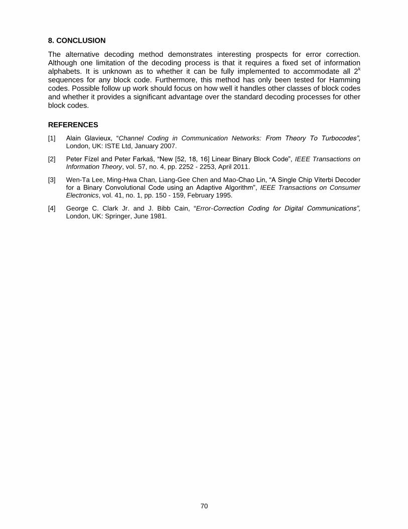
70
8. CONCLUSION
The alternative decoding method demonstrates interesting prospects for error correction. Although one limitation of the decoding process is that it requires a fixed set of information alphabets. It is unknown as to whether it can be fully implemented to accommodate all 2k sequences for any block code. Furthermore, this method has only been tested for Hamming codes. Possible follow up work should focus on how well it handles other classes of block codes and whether it provides a significant advantage over the standard decoding processes for other block codes.
REFERENCES
[1] Alain Glavieux, “Channel Coding in Communication Networks: From Theory To Turbocodes”, London, UK: ISTE Ltd, January 2007.
[2] Peter Fízel and Peter Farkaš, “New [52, 18, 16] Linear Binary Block Code”, IEEE Transactions on Information Theory, vol. 57, no. 4, pp. 2252 - 2253, April 2011.
[3] Wen-Ta Lee, Ming-Hwa Chan, Liang-Gee Chen and Mao-Chao Lin, “A Single Chip Viterbi Decoder for a Binary Convolutional Code using an Adaptive Algorithm”, IEEE Transactions on Consumer Electronics, vol. 41, no. 1, pp. 150 - 159, February 1995.
[4] George C. Clark Jr. and J. Bibb Cain, “Error-Correction Coding for Digital Communications”, London, UK: Springer, June 1981.
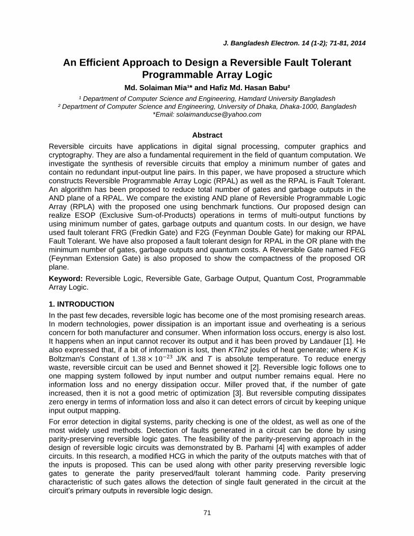
71
J. Bangladesh Electron. 14 (1-2); 71-81, 2014
An Efficient Approach to Design a Reversible Fault Tolerant
Programmable Array Logic
Md. Solaiman Mia¹* and Hafiz Md. Hasan Babu²
¹ Department of Computer Science and Engineering, Hamdard University Bangladesh ² Department of Computer Science and Engineering, University of Dhaka, Dhaka-1000, Bangladesh
*Email: [email protected]
Abstract
Reversible circuits have applications in digital signal processing, computer graphics and cryptography. They are also a fundamental requirement in the field of quantum computation. We investigate the synthesis of reversible circuits that employ a minimum number of gates and contain no redundant input-output line pairs. In this paper, we have proposed a structure which constructs Reversible Programmable Array Logic (RPAL) as well as the RPAL is Fault Tolerant. An algorithm has been proposed to reduce total number of gates and garbage outputs in the AND plane of a RPAL. We compare the existing AND plane of Reversible Programmable Logic Array (RPLA) with the proposed one using benchmark functions. Our proposed design can realize ESOP (Exclusive Sum-of-Products) operations in terms of multi-output functions by using minimum number of gates, garbage outputs and quantum costs. In our design, we have used fault tolerant FRG (Fredkin Gate) and F2G (Feynman Double Gate) for making our RPAL Fault Tolerant. We have also proposed a fault tolerant design for RPAL in the OR plane with the minimum number of gates, garbage outputs and quantum costs. A Reversible Gate named FEG (Feynman Extension Gate) is also proposed to show the compactness of the proposed OR plane.
Keyword: Reversible Logic, Reversible Gate, Garbage Output, Quantum Cost, Programmable Array Logic.
1. INTRODUCTION
In the past few decades, reversible logic has become one of the most promising research areas. In modern technologies, power dissipation is an important issue and overheating is a serious concern for both manufacturer and consumer. When information loss occurs, energy is also lost. It happens when an input cannot recover its output and it has been proved by Landauer [1]. He also expressed that, if a bit of information is lost, then KTln2 joules of heat generate; where K is
Boltzman's Constant of 1.38 × 10⁻²³ J/K and T is absolute temperature. To reduce energy waste, reversible circuit can be used and Bennet showed it [2]. Reversible logic follows one to one mapping system followed by input number and output number remains equal. Here no information loss and no energy dissipation occur. Miller proved that, if the number of gate increased, then it is not a good metric of optimization [3]. But reversible computing dissipates zero energy in terms of information loss and also it can detect errors of circuit by keeping unique input output mapping.
For error detection in digital systems, parity checking is one of the oldest, as well as one of the most widely used methods. Detection of faults generated in a circuit can be done by using parity-preserving reversible logic gates. The feasibility of the parity-preserving approach in the design of reversible logic circuits was demonstrated by B. Parhami [4] with examples of adder circuits. In this research, a modified HCG in which the parity of the outputs matches with that of the inputs is proposed. This can be used along with other parity preserving reversible logic gates to generate the parity preserved/fault tolerant hamming code. Parity preserving characteristic of such gates allows the detection of single fault generated in the circuit at the circuit’s primary outputs in reversible logic design.
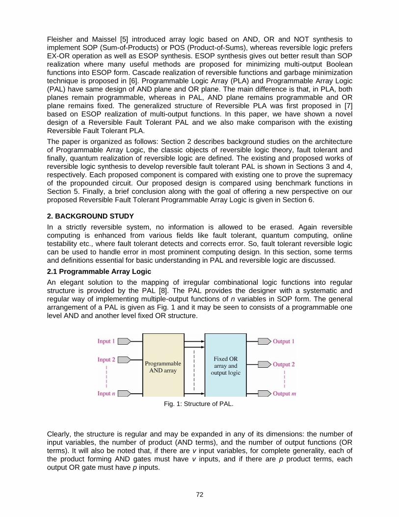
72
Fleisher and Maissel [5] introduced array logic based on AND, OR and NOT synthesis to implement SOP (Sum-of-Products) or POS (Product-of-Sums), whereas reversible logic prefers EX-OR operation as well as ESOP synthesis. ESOP synthesis gives out better result than SOP realization where many useful methods are proposed for minimizing multi-output Boolean functions into ESOP form. Cascade realization of reversible functions and garbage minimization technique is proposed in [6]. Programmable Logic Array (PLA) and Programmable Array Logic (PAL) have same design of AND plane and OR plane. The main difference is that, in PLA, both planes remain programmable, whereas in PAL, AND plane remains programmable and OR plane remains fixed. The generalized structure of Reversible PLA was first proposed in [7] based on ESOP realization of multi-output functions. In this paper, we have shown a novel design of a Reversible Fault Tolerant PAL and we also make comparison with the existing Reversible Fault Tolerant PLA.
The paper is organized as follows: Section 2 describes background studies on the architecture of Programmable Array Logic, the classic objects of reversible logic theory, fault tolerant and finally, quantum realization of reversible logic are defined. The existing and proposed works of reversible logic synthesis to develop reversible fault tolerant PAL is shown in Sections 3 and 4, respectively. Each proposed component is compared with existing one to prove the supremacy of the propounded circuit. Our proposed design is compared using benchmark functions in Section 5. Finally, a brief conclusion along with the goal of offering a new perspective on our proposed Reversible Fault Tolerant Programmable Array Logic is given in Section 6.
2. BACKGROUND STUDY
In a strictly reversible system, no information is allowed to be erased. Again reversible computing is enhanced from various fields like fault tolerant, quantum computing, online testability etc., where fault tolerant detects and corrects error. So, fault tolerant reversible logic can be used to handle error in most prominent computing design. In this section, some terms and definitions essential for basic understanding in PAL and reversible logic are discussed.
2.1 Programmable Array Logic
An elegant solution to the mapping of irregular combinational logic functions into regular structure is provided by the PAL [8]. The PAL provides the designer with a systematic and regular way of implementing multiple-output functions of n variables in SOP form. The general arrangement of a PAL is given as Fig. 1 and it may be seen to consists of a programmable one level AND and another level fixed OR structure.
Clearly, the structure is regular and may be expanded in any of its dimensions: the number of input variables, the number of product (AND terms), and the number of output functions (OR terms). It will also be noted that, if there are v input variables, for complete generality, each of the product forming AND gates must have v inputs, and if there are p product terms, each output OR gate must have p inputs.
Fig. 1: Structure of PAL.
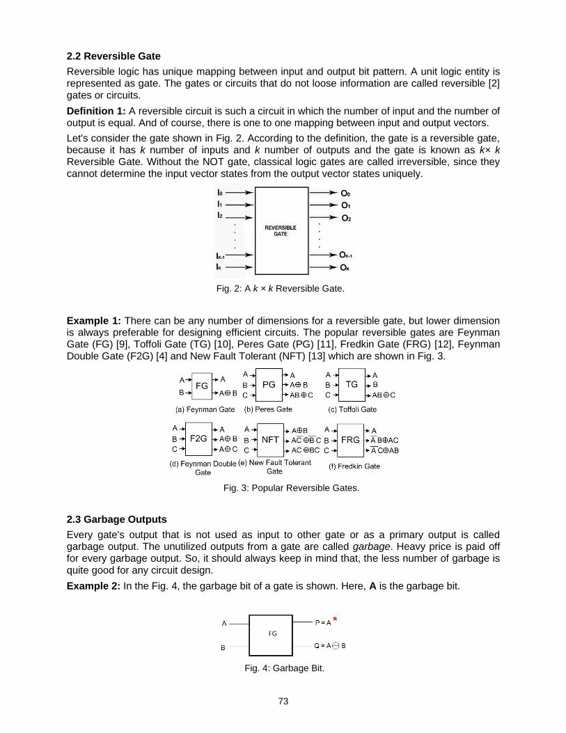
73
2.2 Reversible Gate
Reversible logic has unique mapping between input and output bit pattern. A unit logic entity is represented as gate. The gates or circuits that do not loose information are called reversible [2] gates or circuits.
Definition 1: A reversible circuit is such a circuit in which the number of input and the number of output is equal. And of course, there is one to one mapping between input and output vectors.
Let's consider the gate shown in Fig. 2. According to the definition, the gate is a reversible gate, because it has k number of inputs and k number of outputs and the gate is known as k× k Reversible Gate. Without the NOT gate, classical logic gates are called irreversible, since they cannot determine the input vector states from the output vector states uniquely.
Example 1: There can be any number of dimensions for a reversible gate, but lower dimension is always preferable for designing efficient circuits. The popular reversible gates are Feynman Gate (FG) [9], Toffoli Gate (TG) [10], Peres Gate (PG) [11], Fredkin Gate (FRG) [12], Feynman Double Gate (F2G) [4] and New Fault Tolerant (NFT) [13] which are shown in Fig. 3.
2.3 Garbage Outputs
Every gate's output that is not used as input to other gate or as a primary output is called garbage output. The unutilized outputs from a gate are called garbage. Heavy price is paid off for every garbage output. So, it should always keep in mind that, the less number of garbage is quite good for any circuit design.
Example 2: In the Fig. 4, the garbage bit of a gate is shown. Here, A is the garbage bit.
Fig. 2: A k × k Reversible Gate.
Fig. 3: Popular Reversible Gates.
Fig. 4: Garbage Bit.

74
2.4 Fault Tolerant Procedure: Parity Preserving
There are some causes of circuitry violation. Bit error is one of them. Reversible circuit is able to espouse same parity between input-output bit patterns to provide fault tolerance facility.
2.5 Fault Tolerant Gate
Parity Preserving is a property of reversible logic, where every mapped input and output of a gate preserves same parity: odd or even. Parity preserving is only one method in fault tolerant reversible logic [14].
Definition 2: A reversible gate is fault tolerant which constantly preserves same parity between input and output.
Example 3: Generally, 1 × 1 and 2 × 2 gates are not assumed as fault tolerant. F2G, FRG and NFT gates are 3 × 3 and MIG is 4 × 4 fault tolerant gates.
2.6 Reversible Quantum Computing
Quantum theory is a gigantic research field deeply related to crucial applications as DNA technologies, nanotechnologies and optical computing etc. Reversible quantum logic plays an important role in quantum computing.
Definition 3: The quantum cost of a circuit is the total number of 2 × 2 quantum primitives are used to realize corresponding quantum circuit. Basically, the quantum primitives are matrix operations, which are applied on qubits state.
Example 4: The cost of all 2 × 2 gates are same and it is 1 and 0 for 1 × 1 [15]. Every circuit can be constructed from those 1 × 1 and 2 × 2 quantum primitives and the cost of circuit is the total sum of used 2 × 2 gates [16].
3. EXISTING REVERSIBLE FAULT TOLERANT PROGRAMMABLE LOGIC ARRAY
For recovering the error of reversible circuits, fault tolerant circuit is highly needed. The conversion of the whole non preserving world into fault tolerant will be better if it is started from basic level by realizing popular gates into fault tolerant fashion.
PLA allows SOP for implementing Boolean functions. The typical implementation consists of input buffers, the programmable AND matrix followed by the fixed OR matrix, and output buffers.
Definition 4: PLA consists of two planes: the first one is programmable AND plane and the second one is fixed OR plane known as AND-OR PLA. When the second plane works as EX-OR, then it is called AND-EXOR PLA [7].
PLA and PAL is almost same in architectural design. The PLA has also two planes as AND and OR plane. But the difference between PLA and PAL is: the OR plane of PLA is also programmable as AND plane, but the OR plane of PAL is fixed and the AND plane is programmable.
Since the AND part of PLA and PAL is programmable, we want to make such a design which is fault tolerant as well as minimized in the number of gates, garbage outputs and quantum cost. Before that, we mention here the existing works of PLA.
The beginning work of irreversible PLA is first designed as reversible PLA [7]. Since, it was the first design of reversible PLA, it required more number of gates, garbage outputs and quantum cost. Then, another work is done with reversible PLA for minimizing the total number of gates, garbage outputs and quantum cost [17]. These two designs were not fault tolerant. Finally, the design of reversible fault tolerant PLA is shown in [18].
The AND plane of existing reversible fault tolerant PLA is designed for some multi-output ESOP functions. Assume the functions are:

75
𝐹1 = 𝐴𝐶 𝐴′𝐵′𝐶
𝐹2 = 𝐴𝐵′ 𝐴𝐵′𝐶
𝐹3 = 𝐴𝐵′ 𝐴𝐵′𝐶 𝐵𝐶′
𝐹4 = 𝐴𝐶
𝐹5 = 𝐴𝐵′ 𝐴𝐶 𝐵𝐶′
The products of these functions are:
𝐴𝐶,𝐴𝐵′ ,𝐵𝐶′ ,𝐴𝐵′𝐶,𝐴′𝐵′𝐶
Definition 5: Frequency of a product is the total number of output functions, which will use this product. The Table 1 shows the frequencies of all products of multi-output functions {F1, F2, F3, F4, F5}.
Example 5: Table 1 shows that, the frequency of 𝐴𝐶 is 3 and 𝐴′𝐵′𝐶 is 1.
Table 1: Frequency of Products
Products
Functions Frequency of Products
F1 F2 F3 F4 F5
𝐴𝐵′ x x x 3
𝐴𝐵′𝐶 x x 2
𝐴𝐶 x x x 3
𝐵𝐶′ x x 2
𝐴′𝐵′𝐶 x 1
Definition 6: Number of products of a function is the total number of products that are used to realize the function in ESOP form.
Example 6: The number of products of the function F1 is 2, because two products are required to realize the function F1 in ESOP form. Table 2 shows the number of products of each function individually.
Table 2: Number of Products
Functions F1 F2 F3 F4 F5
Number of Products 2 2 3 1 3
Now, we give different representations of FRG and F2G in Fig. 5, which is used in existing design of reversible fault tolerant PLA [18] as well as we will use in our proposed design.
Fig. 5: Different Gate Representations of Fredkin Gate. and F2G.

76
4. PROPOSED REVERSIBLE FAULT TOLERANT PAL
The existing design of PAL is not reversible as well as not fault tolerant. Our work combines several ideas to present the construction of reversible fault tolerant PAL for multi-output functions by introducing new structure based on F2G and FRG gates, heuristic algorithm for proposed reversible fault tolerant PAL, ordering of functions as well as ordering of products, optimization of EXOR plane and AND plane minimization in terms of products.
In our proposed design, we want to make the reversible PAL as fault tolerant. Since, the AND plane of PLA and PAL is programmable, our proposed algorithm will minimize the number of gates, garbage outputs and quantum cost as compared to previous one [18].
4.1 Proposed Design of AND Plane of Reversible Fault Tolerant PAL
As mentioned earlier, PAL has two planes: AND plane and EX-OR plane. In our proposed design, we use two fault tolerant gates: F2G and FRG for designing fault tolerant PAL. F2G is used for copy and complement the gate, and FRG is used for ANDing the inputs as required outputs.
We use the functions described as the existing design of reversible fault tolerant PLA uses. We will design such a circuit which will decrease the total number of gates, garbage outputs and quantum cost. With our proposed work, at first we sort the min-terms by the number of frequencies to decreased order. As a result, when the larger number of functions is copied or complemented, the lower number of functions is automatically generated.
When we do the AND operation using FRG, we take the inputs as two bits. So, for input A and
B, there may be one of four conditions: AB, AB’, A’B, A’B’. If there exist another input along
these terms, then the rest part of the input must have only one of the two forms: (The previous
form) . C or (The previous form) . C’, if another input is C. The other inputs follow the same rule. This kind of operation will decrease the AND operation and thus will decrease the total number of gates, garbage outputs and quantum cost.
However, the normal design includes all the combination of inputs, that's why our proposed design is better than existing design [18].
We follow an algorithm for designing the AND plane of our proposed reversible fault tolerant PAL. The algorithm is given in Algorithm 1. Here, F2G and FRG are used for different combinations. In our proposed design, we also use the gates 1, 2 and 3 which are shown in Fig. 5. Our proposed AND plane design of reversible fault tolerant PAL is given in Fig. 6.
Algorithm 1 Algorithm for designing the AND plane of our proposed reversible fault tolerant PAL
1. START
a. Sort Min-terms
b. TG := 0 [TG = Total Number of Gates]
c. Put all literals into the Stack
d. Repeat Step 1.d.i for each ordered Product (𝑃𝑖)
i. if Product (𝑃𝑖) is the single literal then
1. Apply F2G Gate
2. Increment Number of Gates
3. Update Stack
ii. End if
iii. else
1. if Two literals are Complemented then

77
a. Apply F2G and FRG Gates
b. Increment Number of Gates
c. Update Stack
2. End if
3. if Two literals are in Normal Form then
a. Apply F2G and FRG Gates
b. Increment Number of Gates
c. Update Stack
4. End if
5. if One literal is Complemented and Another is in Normal Form
then
a. Apply F2G and FRG Gates
b. Increment Number of Gates
c. Update Stack
6. End if
iv. End if
e. End Repeat
2. END
Table 3: Comparison of Efficiency Parameters between Proposed and Existing Designs of AND plane of Reversible Fault Tolerant PAL
Total Gates Garbage Outputs Quantum Cost
Existing [18] 10 11 41
Proposed 9 9 39
In Table 3, we have shown that, for some assuming functions, our proposed design is quite good, since it requires less number of reversible gates, garbage outputs and quantum cost.
4.2 Proposed Design of OR Plane of Reversible Fault Tolerant PAL
The OR plane of PAL is not programmable. So, when designing, we keep in mind that, we cannot change the pattern of OR plane’s input from outside world. The OR plane is fixed. The output from AND plane of PAL is directly used to the input of EX-OR plane.
Fig. 6: Proposed Design of AND Plane of Reversible Fault Tolerant PAL.

78
For designing the OR plane of our proposed reversible fault tolerant PAL, we use some other representations of F2G. The representations of F2G are shown in Fig. 7.
Our proposed OR plane design of reversible fault tolerant PAL is given in Fig. 8.
4.3 Proposed Design of Minimized OR plane of a Reversible PAL
The previous subsections have shown the designs of reversible fault tolerant PAL. In the proposed design, for EX-OR plane, we used Feynman Double Gate (F2G). If we use some other gate in the place of F2G of EX-OR plane, then total number of gates, garbage outputs and quantum cost will be minimized compared to earlier design.
Now, we are going to propose a reversible gate called Feynman Extension Gate (FEG) here. With the help of this gate, we can EX-OR any number of inputs. The FEG input and output for $n$ number of EX-OR literals is shown in Fig. 9.
When working, If there exist more input literals of EX-OR plane, then the use of FEG will be the more flexible. Using FEG, if there is N inputs, then we use E(N). For example, if there is 2 inputs, we use E(2), if 3 inputs, we use E(3) etc.
The algorithm for OR plane design of reversible PAL is given in Algorithm 2.
Algorithm 2 Algorithm for designing the OR plane of our proposed reversible fault tolerant PAL
1. START
a. TG := 0 [TG = Total Number of Gates]
b. Calculate the Frequency of Min-terms
Fig. 7: Another Representation of F2G.
Fig. 8: Proposed Design of OR Plane of Reversible Fault Tolerant PAL.
Fig. 9: Feynman Extension Gate.

79
c. Copy Corresponding Min-terms
i. (Suitable Feynman Extension Gate)
d. Increment Number of Gates
e. Apply XOR Operation
i. (Suitable Feynman Extension Gate)
f. Increment Number of Gates
2. END
The proposed design of minimized EX-OR plane of our proposed reversible PAL is shown in Fig. 10.
From Fig. 10, for EX-ORing the input literals come from the AND plane of output functions F1, F2, F3, F4 and F5, we use only two E2 Gates and two E3 Gates. If we want to minimize the number of gates, garbage outputs and quantum cost, we can use this design, but it will not be fault tolerant. The comparison between using F2G and using FEG is given in Table 4.
Table 4: Comparison between F2G and FEG
Using F2G Using FEG
Gate Garbage Quantum Cost
Gate Garbage Quantum Cost
10 10 20 8 6 20
From the comparison shown in Table 4, it does not seem so effective to use FEG in the place of F2G. But, it will be very effective when total number of functions will increased, since with the help of FEG, we can EX-OR any number of literals.
5. COMPARATIVE STUDY
The existing design of reversible fault tolerant PLA [18] and our proposed design of reversible fault tolerant PAL has the same programmable AND plane. So, we compare the AND plane between existing [18] and our proposed design with the benchmark functions [19]. The comparison with the benchmark functions is given in Table 5.
Fig. 10: Proposed Design of EX-OR Plane of PAL.

80
Table 5: Comparison between Existing and Proposed AND plane Design with Benchmark Functions
Function Proposed Existing [18]
Gate Garbage Quantum Cost Gate Garbage Quantum Cost
5xp1 99 97 423 110 104 472
9sym 346 289 1619 363 298 1704
adr1 1 2 5 3 4 9
adr2 12 16 39 14 20 46
adr3 39 41 156 43 47 176
apex1 2553 2253 12138 2615 2298 12448
apex3 1766 1540 8152 1778 1598 8212
b12 119 108 526 121 123 536
bw 65 69 268 66 64 273
clip 334 294 1532 358 303 1694
con1 24 26 96 27 33 111
cordic 10349 8879 50005 10424 8902 50380
duke2 649 598 3062 659 620 3112
e64 2143 2115 10523 2144 2180 10528
table3 1733 1419 8296 1768 1433 8471
table5 1772 1476 8482 1785 1493 8547
z9sym 346 289 1619 363 298 1704
25xp1 102 94 441 111 101 480
xor5 4 8 9 5 14 10
vag2 1741 1591 8309 1768 1616 8444
sao21 212 197 1003 221 207 1048
rd84 232 210 1022 246 218 1092
rd53 32 32 130 36 37 150
rd73 120 110 519 127 117 554
pdc 3020 2452 14329 3023 2468 14341
From Table 5, we can see that the proposed method is quite good, since it requires less number of reversible gates, garbage outputs and quantum cost than the existing ones. For example, existing design [18] for rd84 circuit requires 246 reversible gates with 218 garbage outputs having 1092 quantum cost, whereas our proposed design requires 232 reversible gates with 210 garbage outputs having 1022 quantum cost.
6. CONCLUSION
In this paper, we have shown two kinds of reversible PAL: one is fault tolerant and another is non fault tolerant. Since, the AND plane is programmable as PLA, we have minimized the total number of gates, garbage outputs and quantum cost in our proposed design, which remains fault tolerant as well. When the full architecture of reversible PAL remains fault tolerant, EXOR plane is also fault tolerant and in this case, the reversible PAL requires more number of gates, garbage outputs and quantum cost. However, the proposed non fault tolerant reversible PAL requires less number of gates, garbage outputs and quantum cost. The reversible fault tolerant PAL is useful for designing the digital circuits easily. For example, large functions which have several variables can be easily implemented by using reversible fault tolerant PAL.
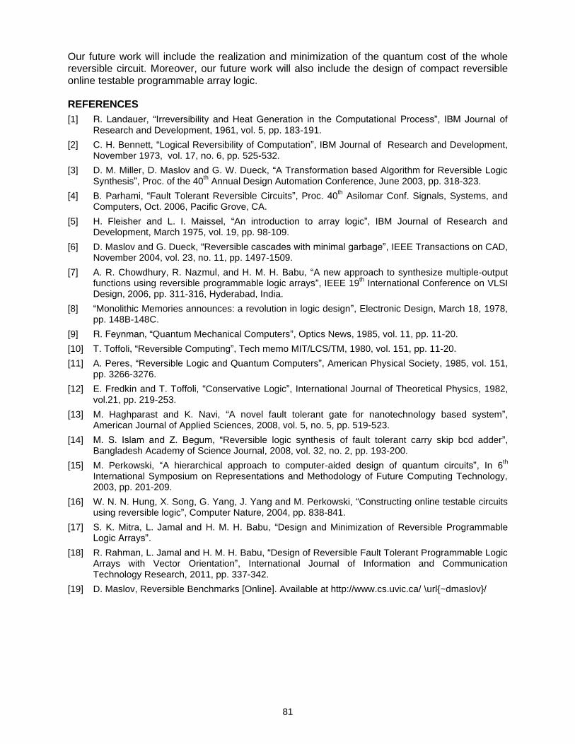
81
Our future work will include the realization and minimization of the quantum cost of the whole reversible circuit. Moreover, our future work will also include the design of compact reversible online testable programmable array logic.
REFERENCES
[1] R. Landauer, “Irreversibility and Heat Generation in the Computational Process”, IBM Journal of Research and Development, 1961, vol. 5, pp. 183-191.
[2] C. H. Bennett, “Logical Reversibility of Computation”, IBM Journal of Research and Development, November 1973, vol. 17, no. 6, pp. 525-532.
[3] D. M. Miller, D. Maslov and G. W. Dueck, “A Transformation based Algorithm for Reversible Logic Synthesis”, Proc. of the 40
th Annual Design Automation Conference, June 2003, pp. 318-323.
[4] B. Parhami, “Fault Tolerant Reversible Circuits”, Proc. 40th Asilomar Conf. Signals, Systems, and
Computers, Oct. 2006, Pacific Grove, CA.
[5] H. Fleisher and L. I. Maissel, “An introduction to array logic”, IBM Journal of Research and Development, March 1975, vol. 19, pp. 98-109.
[6] D. Maslov and G. Dueck, “Reversible cascades with minimal garbage”, IEEE Transactions on CAD, November 2004, vol. 23, no. 11, pp. 1497-1509.
[7] A. R. Chowdhury, R. Nazmul, and H. M. H. Babu, “A new approach to synthesize multiple-output functions using reversible programmable logic arrays”, IEEE 19
th International Conference on VLSI
Design, 2006, pp. 311-316, Hyderabad, India.
[8] “Monolithic Memories announces: a revolution in logic design”, Electronic Design, March 18, 1978, pp. 148B-148C.
[9] R. Feynman, “Quantum Mechanical Computers”, Optics News, 1985, vol. 11, pp. 11-20.
[10] T. Toffoli, “Reversible Computing”, Tech memo MIT/LCS/TM, 1980, vol. 151, pp. 11-20.
[11] A. Peres, “Reversible Logic and Quantum Computers”, American Physical Society, 1985, vol. 151, pp. 3266-3276.
[12] E. Fredkin and T. Toffoli, “Conservative Logic”, International Journal of Theoretical Physics, 1982, vol.21, pp. 219-253.
[13] M. Haghparast and K. Navi, “A novel fault tolerant gate for nanotechnology based system”, American Journal of Applied Sciences, 2008, vol. 5, no. 5, pp. 519-523.
[14] M. S. Islam and Z. Begum, “Reversible logic synthesis of fault tolerant carry skip bcd adder”, Bangladesh Academy of Science Journal, 2008, vol. 32, no. 2, pp. 193-200.
[15] M. Perkowski, “A hierarchical approach to computer-aided design of quantum circuits”, In 6th
International Symposium on Representations and Methodology of Future Computing Technology, 2003, pp. 201-209.
[16] W. N. N. Hung, X. Song, G. Yang, J. Yang and M. Perkowski, “Constructing online testable circuits using reversible logic”, Computer Nature, 2004, pp. 838-841.
[17] S. K. Mitra, L. Jamal and H. M. H. Babu, “Design and Minimization of Reversible Programmable Logic Arrays”.
[18] R. Rahman, L. Jamal and H. M. H. Babu, “Design of Reversible Fault Tolerant Programmable Logic Arrays with Vector Orientation”, International Journal of Information and Communication Technology Research, 2011, pp. 337-342.
[19] D. Maslov, Reversible Benchmarks [Online]. Available at http://www.cs.uvic.ca/ \url{~dmaslov}/

83
J. Bangladesh Electron. 14 (1-2); 83-91, 2014
Teaching Electrical Circuit Course for Electrical Engineering
Students in Cognitive Domain
Muhibul Haque Bhuyan
Department of Electrical and Electronic Engineering, Green University of Bangladesh, Dhaka E-mail: [email protected]
Abstract
Electrical Circuit course is the elementary course for the students of undergraduate program of electrical and electronic engineering. Most of the engineering disciplines also require this course in undergraduate level. This course also has some real life applications in many engineering tasks. Therefore, ‘Electrical Circuit’ course shall be taught efficiently so that students can apply the knowledge earned from this course in solving their practical problems. Skills in the cognitive domain of Bloom's Taxonomy revolve around knowledge, comprehension, and critical thinking of a particular topic. This makes teaching and learning more effective and efficient. In this paper, the teaching method of ‘Electrical Circuit’ course for undergraduate electrical and electronic engineering students in the cognitive domain has been described.
Keywords: Electrical Circuit, Teaching Methods, Bloom’s Taxonomy, Cognitive Domain.
1. INTRODUCTION
In most of the engineering disciplines electrical circuit analysis course is an elementary course. This course has direct practical applications. Without the knowledge of this course it is not possible for an engineer to design and develop any electrical circuits or networks or any electronic controllers. A recent trend in undergraduate engineering education is the incorporation of introductory engineering courses in the freshman year [1]. Therefore, ‘Electrical Circuit’ course is a very important and useful course in the curriculum of the undergraduate electrical and electronic engineering (EEE) program and is incorporated in the first term of the freshmen year and occupies the core position in EEE curriculum. It is designed to teach the students basic laws of electricity and magnetism, various network theorems for solving various electrical networks and for computing its parameters [2-3].
Learning is an activity that leads to change and control of what is taught, while teaching is a practical activity or action, be intentional and conscious to assist learning. Teachers should act an essential role as a facilitator in the process of teaching and learning. So, the electrical circuit course shall be designed and taught in such a way so that the students are prepared to master various laws, formulas and theorems related to electrical circuits for designing the real-time electrical networks and systems by learning properly [4].
Any engineering program should be mandated by an accreditation agency (such as, in USA it is EAC/ABET) and the accreditation of an engineering program will be judged with respect to the defined program outcomes. Each program must have an assessment process for continuous improvement with documented results. Any well thought course required for an engineering degree should be able to contribute towards fulfilling the program educational objectives, which are mandated by the ABET criteria 2000 [5].
Currently, the education system is undergoing rapid changes. Various new methods are introduced and used. Further, it makes teaching more effective and learning is highly significant. An important goal of the undergraduate curriculum in engineering is to develop the integration, design, and evaluation capabilities of the student. As shown in Fig. 1, Bloom in 1956 characterized the six cognitive levels in the hierarchy: Knowledge Comprehension Application Analysis Synthesis Evaluation. The cognitive skills at the highest level are synthesis and evaluation, which rely on comprehension, application, and analysis capabilities in
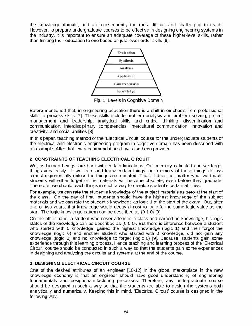
84
the knowledge domain, and are consequently the most difficult and challenging to teach. However, to prepare undergraduate courses to be effective in designing engineering systems in the industry, it is important to ensure an adequate coverage of these higher-level skills, rather than limiting their education to one based on just lower order skills [6].
Fig. 1: Levels in Cognitive Domain
Before mentioned that, in engineering education there is a shift in emphasis from professional skills to process skills [7]. These skills include problem analysis and problem solving, project management and leadership, analytical skills and critical thinking, dissemination and communication, interdisciplinary competencies, intercultural communication, innovation and creativity, and social abilities [8].
In this paper, teaching method of the ‘Electrical Circuit’ course for the undergraduate students of the electrical and electronic engineering program in cognitive domain has been described with an example. After that few recommendations have also been provided.
2. CONSTRAINTS OF TEACHING ELECTRICAL CIRCUIT
We, as human beings, are born with certain limitations. Our memory is limited and we forget things very easily. If we learn and know certain things, our memory of those things decays almost exponentially unless the things are repeated. Thus, it does not matter what we teach, students will either forget or the materials will become obsolete, even before they graduate. Therefore, we should teach things in such a way to develop student’s certain abilities.
For example, we can rate the student’s knowledge of the subject materials as zero at the start of the class. On the day of final, students should have the highest knowledge of the subject materials and we can rate the student’s knowledge as logic 1 at the start of the exam. But, after one or two years, that knowledge would decay almost to logic 0, the same logic value as the start. The logic knowledge pattern can be described as {0 1 0} [9].
On the other hand, a student who never attended a class and earned no knowledge, his logic states of the knowledge can be described as {0 0 0}. But there is difference between a student who started with 0 knowledge, gained the highest knowledge (logic 1) and then forgot the knowledge (logic 0) and another student who started with 0 knowledge, did not gain any knowledge (logic 0) and no knowledge to forget (logic 0) [9]. Because, students gain some experience through this learning process. Hence teaching and learning process of the ‘Electrical Circuit’ course should be conducted in such a way so that the students gain some experiences in designing and analyzing the circuits and systems at the end of the course.
3. DESIGNING ELECTRICAL CIRCUIT COURSE
One of the desired attributes of an engineer [10-12] in the global marketplace in the new knowledge economy is that an engineer should have good understanding of engineering fundamentals and design/manufacturing processes. Therefore, any undergraduate course should be designed in such a way so that the students are able to design the systems both analytically and numerically. Keeping this in mind, ‘Electrical Circuit’ course is designed in the following way.

85
A. Course Contents
This gives the complete description of the course. The course contents should be designed in such a way so that the students get a deep knowledge and develop their skills to apply the knowledge in their fields and course objectives are achieved. Incorporation of too many topics in the course may impede the students’ learning objectives. So, the optimal contents for ‘Electrical Circuit’ course are set as follows:
Circuit variables and elements: voltage, current, power, energy, independent and dependent sources, resistance. Basic laws: Ohm’s law, Kirchhoff’s current and voltage laws. Simple resistive circuits: series and parallel circuits, voltage and current division, wye-delta transformation. Techniques of circuit analysis: node and mesh analysis including super node and super mesh. Network theorems: source transformation, Thevenin’s, Norton’s and
Superposition Theorems with applications in circuits having independent and dependent sources, maximum power transfer theorem and reciprocity theorem. Energy storage elements: inductors, capacitors and their series parallel combination. Responses of RL and RC circuits: natural and step responses.
Magnetic quantities and variables: flux, permeability and reluctance, magnetic field strength, magnetic potential, flux density, magnetization curve. Laws in magnetic circuits: Ohm’s law and Ampere’s circuital law. Magnetic circuits: series, parallel and series-parallel circuits.
B. Course Objectives
Learning objectives or instructional objectives are statements of what students should be able to do if they have acquired the knowledge and skills the course is supposed to teach them. The objectives of ‘Electrical Circuit’ course have been set as follows:
1. To know the basic elements of the electrical circuits.
2. To know the various types of electrical signals.
3. To know and understand various laws of electrical circuits
4. To apply various theorems to solve the problems of electrical circuits and to interpret the results
5. To find the various parameters from electrical circuits
6. To determine the transient response in electrical circuits
7. To analyze the magnetic circuits
8. To sketch various types of electrical and magnetic circuits.
C. Course Outcomes
Course outcomes or learning outcomes reflect the degree to which the program has met its objectives; outcome indicators, the assessment instruments and procedures that will be used to determine whether the graduates have achieved the outcomes. After successful completion of the ‘Electrical Circuit’ course with a minimum grade of ‘C+’, the students will be able to
1. Identify and use of various electrical circuit elements
2. Draw the various types of electrical circuits using symbols
3. Simplify and design various electrical circuits
4. Find out the parameter values in electrical circuits
5. Apply various laws and theorems of electrical circuits to solve the problems
6. Predict the transient responses and hence its parameters
7. Design magnetic circuits
8. Apply laws of magnetic circuits
9. Perform various numerical computations of circuits.

86
4. BLOOM’S TAXONOMY
The idea for this classification system was formed at an informal meeting of college examiners attending the 1948 American Psychological Association Convention in Boston. At this meeting, interest was expressed in a theoretical framework which could be used to facilitate communication among examiners. This group felt that such a framework could do much to promote the exchange of test materials and ideas about testing. In addition, it could be helpful in stimulating research on examining and on the relations between examining and education. After considerable discussion, there was agreement that such a theoretical framework might best be obtained through a system of classifying the goals of the educational process, since educational objectives provide the basis for building curricula and tests and represent the starting point for much of our educational research [13].
Bloom's Taxonomy is a classification of learning objectives within education proposed in 1956 by a committee of educators chaired by Benjamin Bloom. Although named after Bloom, the publication followed a series of conferences from 1949 to 1953, which were designed to improve communication between educators on the design of curricula and examinations [14].
It refers to a classification of the different objectives that educators set for the students, i.e. the learning objectives. Bloom's Taxonomy divides educational objectives into three domains: Cognitive, Affective and Psychomotor (sometimes loosely described as knowing/head, feeling/heart and doing/hands respectively). Within the domains, learning at the higher levels is dependent on having attained prerequisite knowledge and skills at lower levels [15]. A goal of Bloom's Taxonomy is to motivate educators to focus on all three domains, creating a more holistic form of education. A revised version of the taxonomy was created in 2000 [16-18].
Bloom also considered the initial effort to be a starting point, as evidenced in a memorandum from 1971 in which he said, “Ideally each major field should have its own taxonomy in its own language - more detailed, closer to the special language and thinking of its experts, reflecting its own appropriate sub-divisions and levels of education, with possible new categories, combinations of categories and omitting categories as appropriate” [16].
Skills in the cognitive domain revolve around knowledge, comprehension, and critical thinking of a particular topic. Traditional education tends to emphasize the skills in this domain, particularly the lower-order objectives. There are six levels in the taxonomy, moving through the lowest order processes to the highest. Through these six processes a student gains knowledge and skills and is able to solve real life problems of their fields of interest. Therefore, to teach the ‘Electrical Circuits’ course for the undergraduate electrical and electronic engineering students, cognitive domain has been selected for teaching and learning process.
5. COURSE OUTCOME ACHIEVEMENT IN COGNITIVE DOMAIN
To determine the achievement of the course outcomes in the cognitive domain it is first necessary to analyze the educational objectives and corresponding learning abilities of the students at different levels of the cognitive domain. These are given in Table I. To illustrate that these educational objectives have been achieved in the ‘Electrical Circuit’ course, the teaching
and learning process of ‘Superposition Theorem’ has been selected [2] from the course content of the ‘Electrical Circuit’ course. The student will first learn the superposition theorem and then solve various types of electrical circuits to understand the use of the theorem. One circuit is shown in Fig. 2 where one voltage and one current source exist. So, it can be solved using the superposition theorem [3].
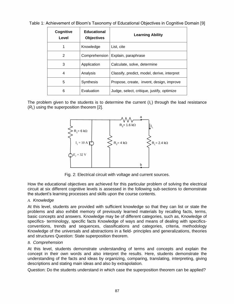
87
Table 1: Achievement of Bloom’s Taxonomy of Educational Objectives in Cognitive Domain [9]
Cognitive
Level
Educational
Objectives Learning Ability
1 Knowledge List, cite
2 Comprehension Explain, paraphrase
3 Application Calculate, solve, determine
4 Analysis Classify, predict, model, derive, interpret
5 Synthesis Propose, create, invent, design, improve
6 Evaluation Judge, select, critique, justify, optimize
The problem given to the students is to determine the current (IL) through the load resistance (RL) using the superposition theorem [2].
IL
R3= 1.6 k
a
b
R1= 6 k
R2= 4 k
E1 = 32 V
RL= 2.4 kI
1 = 10 A
Fig. 2: Electrical circuit with voltage and current sources.
How the educational objectives are achieved for this particular problem of solving the electrical circuit at six different cognitive levels is assessed in the following sub-sections to demonstrate the student’s learning processes and skills upon the course contents.
A. Knowledge
At this level, students are provided with sufficient knowledge so that they can list or state the problems and also exhibit memory of previously learned materials by recalling facts, terms, basic concepts and answers. Knowledge may be of different categories, such as, Knowledge of specifics- terminology, specific facts Knowledge of ways and means of dealing with specifics- conventions, trends and sequences, classifications and categories, criteria, methodology Knowledge of the universals and abstractions in a field- principles and generalizations, theories and structures Question: State superposition theorem.
B. Comprehension
At this level, students demonstrate understanding of terms and concepts and explain the concept in their own words and also interpret the results. Here, students demonstrate the understanding of the facts and ideas by organizing, comparing, translating, interpreting, giving descriptions and stating main ideas and also by extrapolation.
Question: Do the students understand in which case the superposition theorem can be applied?

88
C. Application
At this level, students apply the learned information to solve a problem, to calculate or to solve for the required value. The students also solve problems to new situations by applying acquired knowledge, facts, techniques and rules in a different way.
Question: Can the students calculate equivalent resistance?
D. Analysis
At this level, students break things down into their elements, formulate theoretical explanations or mathematical or logical models for observed phenomena, derive or explain something by identifying motives or causes. They make inferences and find evidence to support generalizations. They also do analysis of elements, analysis of relationships or analysis of organizational principles.
Question: What are the steps required to solve the problem?
E. Synthesis
At this level, students create something combining elements in novel ways; formulate an alternative to the existing design. They also compile information together in a new pattern to produce a unique communication or to propose a set of operations or to derive a set of abstract relations.
Question: Can the students follow the steps to determine the current supplied by the two sources and hence overall load current (IL) through the load resistance (RL)?
F. Evaluation
At this level, students make and justify the values obtained by judgment or select an appropriate value among the various alternatives and also determine which one is better and explain its reasoning, analyze the values critically for accuracy and precision. They also opine by making judgments about information, validity of ideas or quality of work based on a set of criteria or evidences.
Question: Can the students find the overall load current (IL) through the load resistance (RL) for another circuit?
Course outcome achievement is measured through the continuous assessment of all the students in the ‘Electrical Circuit” course. This is a three (3.0) credit, three (3.0) hour course and two (2) classes of 1.5 hours duration are conducted per week in a semester of 13 weeks excluding the mid-term and final examination weeks. For the continuous assessment the following marks distribution is followed:
Attendance: 10 %
Assignment: 10 %
Quizzes: 10 %
Mid-term: 30 %
Final Exam: 40 %
Total: 100 %
Marks are given in attendance if a student is present at least 75% of the classes conducted in the course and if a student is present 100% of the conducted classes then he/she got 10 marks and for each 5% less attendance then 0.5 marks are deducted from 10. Two assignments- one on network theorems and another on magnetic circuits are given each having 5 marks. Two quizzes are taken each having 10 marks and the best one is counted. One and a half hour mid-term examination was taken in the middle of the semester. Student has to answer any three out of four questions given. Comprehensive final examination was taken with duration of two hours at end of the semester and a student has to answer four out of five questions given. Questions on circuit solving, wave shape sketching, circuit designing and mathematical derivations on different network theorems are given both in mid-term and final examinations.

89
Based on the accumulated score final grades of the course are awarded as per grading policy given Table II. It is to be mentioned that this uniform grading policy is approved by the University Grants Commission (UGC) of Bangladesh.
Table 2: Grading Policy
Marks out of 100 Grade Grade Point
80 - 100 A+ 4.00
75 - 79 A 3.75
70 - 74 A- 3.50
65 - 69 B+ 3.25
60 - 64 B 3.00
55 - 59 B- 2.75
50 - 54 C+ 2.50
45 - 49 C 2.25
40 - 44 D 2.00
< 40 F 0.00
As a case study, two batches of students (Batch 1 and 2) of the ‘Electrical Circuit’ course, having equal class size of 34, are considered in two different consecutive semesters (Fall and Spring) of Electrical and Electronic Engineering Department of Green University of Bangladesh. In batch 1, traditional teaching approach is followed in Fall semester and in batch 2, teaching is given in cognitive domain in Spring semester by the same teacher. At the end of the final examinations of the two batches, statistical analyses of the grade points are calculated as shown in Tables III-VI.
Table 3: Grade Distribution of Batch 1
Grades No of Students
A+ 1
A 0
A- 1
B+ 2
B 1
B- 2
C+ 5
C 5
D 7
F 10
Total 34
Table 4: Statistics of Grade Points of Batch 1
Statistical Parameter Value
Mode 0.00
Median 2.13
Mean 1.77
Standard Deviation 1.24
Quartile1 0.00
Quartile3 2.50
Average Deviation 1.04
Class CGPA 1.77

90
Table 5: Grade Distribution of Batch 2
Grades No of Students
A+ 1
A 1
A- 4
B+ 4
B 9
B- 4
C+ 3
C 1
D 1
F 6
Total 34
Table 6: Statistics of Grade Points of Batch 2
Statistical Parameter Value
Mode 3.00
Median 3.00
Mean 2.49
Standard Deviation 1.25
Quartile1 2.50
Quartile3 3.25
Average Deviation 0.92
Class CGPA 2.49
From the tables, it is observed that the statistics have improved in batch 2, where cognitive process is applied for teaching the students, than that in batch 1. Comparing tables III and V, it is observed that the number of students getting the lowest grade (i.e., “F”) has decreased whereas the number of students getting the upper grades (i.e. “A+”/ “A”/ “A-”) has increased in batch 2 than that in batch 1. Comparing tables IV and VI, it is observed that the mode, median, mean, class CGPA etc. have also increased in batch 2 than that in batch 1. Besides, average deviation has is reduced in batch 2. So, the cognitive process of teaching seems to be better.
6. CONCLUSION
The engineering graduates must be well prepared in the changing global competitive knowledge-based industry. Like all of us in the world, the engineering graduates must have the ability for knowledge management. Therefore, universities are facing challenges as well as opportunities for creating and transferring knowledge to the students in efficient and smart way for their survival.
This paper describes the teaching and learning method of ‘Electrical Circuit’ course for electrical and electronic engineering students in cognitive domain, a critical learning domain that includes the recall of knowledge and cultivation of intellectual skills. Certain cognitive processes, such as, problem solving, critical thinking, reasoning, analysis and evaluations are very important in engineering tasks. Since ‘Electrical Circuit’ is an elementary core course in the curriculum of undergraduate electrical and electronic engineering and most other engineering programs, therefore, this course must be taught in such a way so that the students are able to develop
91
their knowledge and skills on designing and analysis of various types of electrical circuits or networks in their real life engineering works.
REFERENCES
[1] B. Carlson, P. Schoch, M. Kalsher and B. Racicot, “A Motivational First-year Electronics Lab Course”, ASEE Journal of Engineering Education, Vol. 86, No. 4, pp. 357-362, October 1997.
[2] R. L. Boylestad and L. Nashelskey, “Introductory Circuit Analysis,” Prentice Hall, USA, 11th edition,
ch. 1, 2011.
[3] C. K. Alexander and M. N. O. Sadiku, “Fundamentals of Electric Circuits,” McGraw Hill, USA, ch. 1, 2009-2010.
[4] S. Choi and M. Saeedifard, “An Educational Laboratory for Digital Control and Rapid Prototyping of Power Electronic Circuits,” IEEE Trans. On Education, vol. 55, no. 2, pp. 263-270, May 2012
[5] “Criteria for Accrediting Engineering Programs,” Engineering Accreditation Commission of the Accreditation Board for Engineering and Technology (EAC/ABET), 2004. http://www.abet.org/
[6] D. R. Lewin, W. D. Seider and J. D. Seader, “Integrated Process Design Instruction”, Computers and Chemical Engineering, vol. 26, no. 2, 2002, pp. 295-306.
[7] R. M. Felder and R. Brent, “The ABC’s of Engineering Education: Abet, Bloom’s Taxonomy, Cooperative Learning, And So on,” Proceedings of the 2004 American Society for Engineering Education Annual Conference & Exposition, American Society for Engineering Education, 2004, pp. 1375-1386.
[8] S. Kuru, “Problem Based Learning”, TREE – Teaching and Research in Engineering in Europe: Problem based and project oriented learning, Isik University, 2007, pp. 1-44.
[9] M. H. Rashid, “Cognitive-Based Teaching of Power Electronics,” Proc. of the 5th International
Conference on Electrical and Computer Engineering (ICECE), 20-22 December 2008, Dhaka, Bangladesh, pp. 883-886.
[10] M. H. Rashid, “Improving Engineering Education,” Proc. of the 3rd
International Conference on Electrical and Computer Engineering (ICECE), 28-30 December 2004, Dhaka, Bangladesh, pp. 1-5.
[11] J. A. White, “Defining the Knowledge Economy,” ABET Annual Meeting, Incline Valley, Nevada, November 1, 2001.
[12] D. O Swain, “Global Corporations Leveraging Knowledge”, ABET Annual Meeting, Incline Valley, Nevada, November 1, 2001.
[13] B. S. Bloom, M. D. Engelhart, E. J. Furst, W. H. Hill and D. R. Krathwohl, “Taxonomy of educational objectives: the classification of educational goals; Handbook I: Cognitive Domain,” Longman Group Ltd, London, 1956.
[14] B. S. Bloom, “Reflections on the development and use of the taxonomy,” in L. W. Anderson and A. S. Lauren, eds. “Bloom's Taxonomy: A Forty-Year Retrospective,” Chicago National Society for the Study of Education, 1994.
[15] Orlich, et al. “Teaching Strategies: A Guide to Effective Instruction,” 2004.
[16] L. W. Anderson, D. R. Krathwohl, P. W. Airasian, K. A. Cruikshank, R. E. Mayer, P. R. Pintrich, J. Raths and M. C. Wittrock (eds), “A Taxonomy for Learning, Teaching, and Assessing: A Revision of Bloom's Taxonomy of Educational Objectives,” 2000.
[17] L. Anderson and D. A. Krathwohl, “Taxonomy for Learning, Teaching and Assessing: A Revision of Bloom's Taxonomy of Educational Objectives,” Longman, New York, 2001.
[18] D. R. Krathwohl, “A revision of bloom's taxonomy: An overview. Theory into Practice,” vol. 41, no. 4, pp. 212-218, 2002.

93
J. Bangladesh Electron. 14 (1-2); 93-99, 2014
FPGA based Nuclear Radiation Counting System
Mohaimina Begum, Abdullah Al Mamun
Atiar Rahman and Anisa Begum
Atomic Energy Center, Dhaka, BAEC E-mail: [email protected]
Abstract
FPGA (Field Programmable Gate Array) devices can make reconfigurable hardware which is high precision and faster. For its successful applications in a verity of area, FPGA devices are used for various instrumentation control system. In this paper, FPGA based Nuclear Radiation Counting System is presented. Hardware configurable nuclear counter is designed and developed to improve the performance and flexibility of the system compared with traditional approaches. In this work, a new technique has been implemented for changing window between ULD and LLD without hardware modification and it can be easily changed by software control. To check this technique electric pulse from the detector and this pulse goes out by preamplifier and feed to ADC through a processing circuit. When the ADC output value is between higher than lower threshold value (LLD) and lower than higher threshold value (ULD) then counter counts those values over a period of one minute and stores the counting value in register. Finally the stored counting values are displayed on LCD. Associate firmware has been developed by Xilinx ISE Design suite 9.2 using VHDL code and tested on Xilinx Spartan 3E Starter board. This developed system can be effectively used for radiation monitoring of human body as well as environment.
Keywords: FPGA, SCA, Gaussian pulse, VHDL
1. INTRODUCTION
The nuclear radiation can not be detected by human senses, therefore need equipment, so called "Nuclear Counting System" to detect and measure that radiation. Nuclear Counting System is used for measuring the nuclear radiation by counting the electric pulses, which are produced by the detector. Number of output pulses is proportional to the number of incoming radiation. This system has a lower and an upper level discriminator and produces an output logic pulse whenever an input pulse falls between the discriminator levels. With this device all voltage pulses in a specific range can be selected and counted by counter [3].
In existing counting system if we want to change window between ULD and LLD for different radiation source, hardware modification is needed which is less flexiblility. Since this design is FPGA based which can be reconfigured by software then it is more flexible than existing counting system. Beacuse of radiation heazards so many dieseases occur and in the long run death. This system is an easy and efficient way for radiation detection and counting.
Many researchers have reported their design and application on FPGA based system, MCA and SCA related things. For example A. Ezzatpanah Latifi developed design and construction of an accurate timing Single Channel Analyzer [5]. Amitkumar Singh designed and simulated a system on FPGA Based Digital Multi Channel Analyzer for Nuclear Spectroscopy Application [6]. From this scientific information; the proposed system was focused on a new technology applied in Nuclear Counting System. As the system can be made possible by a single FPGA chip it takes less time to modify design and it will also be cost effective.
2. DESIGN SCENARIO
Basic Scenario of the designed nuclear counting system is shown in Fig.1. The designed system consists of GM tube, high voltage supply for GM tube, amplifier, discriminator, counter,

94
timer and display unit. The discriminator will produce a TTL logic signal, when the incoming pulse fulfills the energy range criteria, which is defined by the user selectable lower- and upper level. Counters are used for counting the logic signal from the discriminator for certain interval time (counting time). User sets the counting time through the timer in order of seconds, minutes or hours.
Fig.1: Block diagram of the designed Nuclear Counting System
In traditional system for Single channel analyzer (SCA) design needs individual circuit for amplifier, descriminator, counter and timer but in FPGA based system it is possible to design all these circuits in a single system as an integrated device.
3. SYSTEM METHODOLOGY
In this paper, we present the detector (GM), HVPS and FPGA implementation of SCA. The designed system was implemented by using ISE foundation 9.2 and VHDL. Fig. 3 shows functional block diagram of ADC and gain amplifier for amplifier, pulse detector works as discriminator and selects the voltage level for window. Two16 bit counters and pre divider are used for count and set time respectively. Project Specification is as shown in table I.
Table 1: Specification of the Project components
Sl. No. Components name Quantity Description
1. Detector (GM Tube) 1 Halogen GAS Model 712
2. HVPS 1 550 Volt
3. Xilinx FPGA 1 XC3S500E FG-320Spartan-3E FPGA
4. ADC 1 LT1407A
5. Programmable-gain amplifier
1 LTC6912
6. Clock oscillator 1 50 MHz Oscillator CLK_50MHz: (C9)
7. LCD 1 Character LCD
8. LED 8 Eight discrete LEDs
Detector: Geiger-Muller (GM) tube is used to detect radioactive particles. When radiation hits in the window of GM tube, it converts radiation energy into electrical pulse and it is amplified by preamplifier. This GM tube specifications are as a thin end window (e.g. made of mica GM Tube); (Halogen GAS Model 712) for β-ray, γ-ray measure (LND, INC. USA); Tube Bias Voltage; + 550 Volt.
95
HVPS: High Voltage Power Supply (HVPS) is used for the Detector (Geiger Muller Tube) and this high voltage is adjusted for better performance for detector and it is adjusted in the following procedure. Min 400 - Max 600 Volt, Step size 50 Volt was applied at GM tube & source to detector distance 18 cm were used.1min x 3 time’s counts, Average Counts were taken and finally the high voltage is adjusted 550 for this detector.
Fig.2: Detector Plateau measurement Curve
FPGA based SCA:
The following section presents a description of the various components of SCA system in fig. 3. These components are configured by FPGA including SPI interface which connects the FPGA to major external devices gain amplifier and ADC. The other components in the developed system have been designed by FPGA using VHDL code.
Fig. 3: Block diagram of FPGA based SCA
Gain Amplifier and ADC: The Spartan-3E Starter Kit board includes an SPI-compatible, two channels Analog-to-Digital Converter (ADC) and a Gain amplifier (programmable scaling pre-amplifier) which works as analog IO.
Fig.4: Detail view of analog IO circuit [1]

96
The analog IO circuit consists of a Linear Technology LTC6912-1 programmable gain amplifier that scales the incoming analog signal on header J7 (Figure 4). The output of pre-amplifier connects to a Linear Technology LTC1407A-1 ADC [1]. Both the pre-amplifier and the ADC are serially programmed or controlled by the FPGA. The SPI_MOSI, SPI_MISO, and SPI_SCK signals are the bus interface signals between the FPGA, ADC and the gain amplifier. The AMP_CS signal is the active-Low slave select input to the amplifier. The analog IO circuit converts the analog voltage to a 14-bit digital representation. [1].
Discriminator: When the ADC output value is between higher than lower threshold value (LLD) and lower than higher threshold value (ULD), then pulse detector gives the peak found signal to the counter to increase the count value. In this design ULD and LLD is set for window as a Voltage Range is LLD = 800 m Volt and ULD = 1600 m Volt.
Counter: When pulse detector found peak, it provides a peak found signal to counter and as a result, count value increases. Two 16 bit counters are used in counter circuit. One of the counters counts over a period of one minute and stores the counting value in register and another one is used for total count.
Timer: on board 50MHz clock frequency is pre divided to 1 minute for using reset 16 bit Counter and data held in Latch.
Display: Finally the stored counting values are given to LCD through other necessary processing circuits. In addition, maximum peak value, total counts and counts per minute are also displayed to LCD through LCD driver circuit.
4. SOFTWARE DESCRIPTION
All the units of SCA in the system were designed by FPGA using VHDL. These units were described in VHDL-modules and synthesized by Xilinx ISE Design suite 9.2 using the VHDL language. The System has been implemented on Xilinx Spartan-3E Starter board. The flow diagram of the VHDL code and RTL schematic with all entities and components of SCA is shown in the following Fig.5and 6.
Fig. 5: Flow diagram of FPGA based SCA Fig. 6: RTL Schematic after simulation
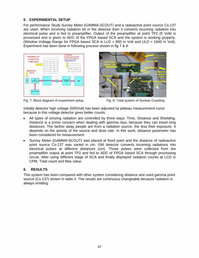
97
5. EXPERIMENTAL SETUP
For performance Study Survey Meter (GAMMA-SCOUT) and a radioactive point source Cs-137 are used. When incoming radiation hit in the detector then it converts incoming radiation into electrical pulse and is fed to preamplifier. Output of the preamplifier at point TP2 (5 Volt) is processed and is given to ADC of the FPGA based SCA and the system is working properly. (Window Voltage Range for FPGA based SCA is LLD = 800 m Volt and ULD = 1600 m Volt). Experiment has been done in following process shown in fig 7 & 8.
Fig. 7: Block diagram of experiment setup Fig. 8: Total system of Nuclear Counting
Initially detector high voltage (550Volt) has been adjusted by plateau measurement curve because in this voltage detector gives better counts.
All types of ionizing radiation are controlled by three ways: Time, Distance and Shielding. Distance is a prime concern when dealing with gamma rays, because they can travel long distances. The farther away people are from a radiation source, the less their exposure. It depends on the activity of the source and dose rate. In this work, distance parameter has been considered for measurement.
Survey Meter (GAMMA-SCOUT) was placed at fixed point and the distance of radioactive point source Cs-137 was varied in cm. GM detector converts incoming radiations into electrical pulses at different distances (cm). Those pulses were collected from the preamplifier output at point TP2 and fed to ADC of FPGA based SCA through processing circuit. After using different stage of SCA and finally displayed radiation counts at LCD in CPM, Total count and Max value.
6. RESULTS
This system has been compared with other system considering distance and used gamma point source (Cs-137) shown in table II. The results are continuous changeable because radiation is always emitting.
Distance

98
Table 2: FPGA based system’s result compare with other system
No. of
Observation
Distances in
cm
Survey Meter
(GAMMA - SCOUT)
in µSv/h
After conversion µSv/h
into CPM
(1 µSv/h = 100CPM)
FPGA Based
System
in CPM
1. 18 0.56 56 65
2. 16 0.61 61 71
3. 14 0.93 93 93
4. 10 1.28 128 125
5. 8 1.38 138 130
6. 6 1.68 168 165
7. 5 2.20 220 225
8. 4 2.57 257 255
9. 3 2.90 290 300
10. 2 3.49 349 349
Fig. 9: Two results of the comparison
Here, the results are from the FPGA based Nuclear Counting System is in CPM and Survey Meter (GAMMA-SCOUT) is in µSv/h (1 µSv/h = 100CPM). For convenient of plotting chart all data is taken in CPM is shown in fig 9. FPGA system is showing almost similar result with other system. For fluctuating results, it is recommended that for low range activity, average of the Max and Min Count acceptable.
7. DISCUSSION
This paper has given emphasis on the design, simulation and implementation of FPGA based Nuclear Counting System. As the design is FPGA based so the system has flexibility to configure hardware. This FPGAs based system can replace complex analog nuclear counter circuitry. The VHDL (Hardware Description Language) design for SCA has been developed and tested on Spartan-3E Starter board. Finally a successful result has been carried out by this developed system.
8. CONCLUSION
Counts have been observed for several times. CPM results of FPGA system were compared with the Survey Meter in µSv/h (1 CPM = 0.01 µSv/h). Developed system was compared with survey meter and showed approximately same with other results. A radiation count normally

99
varies at low range of activity. So, it is recommended that at low range count, average of the min and max count is acceptable. This developed nuclear radiation (especially gamma radiation) counting system may be used for diagnostic purposes in medical and research purpose in laboratory.
REFERENCES
[1] Xilinx UG230 Spartan-3E Starter Kit Board User Guide.
[2] Volnei A. Pedroni, Circuit Design with VHDL.
[3] Dudi Hendriyanto Haditjahyono, Introduction to The Nuclear Counting Systems, Education and Training Center – BATAN, October 2004
[4] SELECTED TOPICS IN NUCLEAR ELECTRONICS, A technical document issued by the International Atomic Energy Agency, Vienna, 1986.
[5] A.EZZATPANAH LATIFI1, F. ABBASI DAVANI1**, M. AHRIARI1 AND A. SHARGHI IDO2, DESIGN AND CONSTRUCTION OF AN ACCURATE TIMING SINGLE CHANNEL ANALYZER* Iranian Journal of Science & Technology, Transaction A, Vol. 33, No. A3, Islamic Republic of Iran, 2009
[6] Design and Simulation of Fpgas Based Digital Multi Channel Analyzer for Nuclear Spectroscopy Application, Amitkumar Singh* S. K. Dubey M. G. Bhatia, Department of Physics Department of Physics, India University of Mumbai, India Ameya Centre of Robotics, Andheri, Mumbai, Volume 4, Issue 8, August 2014 ISSN: 2277 128X
101
J. Bangladesh Electron. 14 (1-2); 101-105, 2014
Design of Microcontroller Based Generator Protection Scheme 1Md. Rokonuzzaman and 2Mohammed Hossam-E-Haider
Electrical, Electronic and Communication Engineering Department Military Institute of Science and Technology, Dhaka, Bangladesh
[email protected] and [email protected]
Abstract
Electricity generation is the heart of power system and alternator is widely used for electricity generation. Therefore the protection of alternator is very important for smooth operation of overall power system network. The fault detection and isolation of the faulty section or apparatus from the system is done by using protective devices like fuses or relays in conjunction with the circuit breaker. The differential relay acts as main protection whereas the over current and earth fault relays act as backup protection for the alternator. The backup protection actuates only if the main protection fails. The fault clearance greatly depends on the actuating quantity and operating time of the relay which need to be coordinated with the protective system requirement. The static relay has faster and reliable operation than those of the conventional electromechanical relay. In this paper the microcontroller based protection scheme is designed for alternator protection. The triac performs the task of relay contact whereas the optocoupler provides electrical isolation between input and output sections of this protective scheme. The microcontroller ensures faster and accurate switching of the triac according to the programming logic.
Keywords: Alternator Fault Protection, Fault Detection, Main protection, Back up Protection, Microcontroller Based Protection.
1. INTRODUCTION
The volume of infrastructure of electrical power system is increasing day by day due to
installation of new generation plants along with expansion of transmission and distribution
network. Therefore system protection devices need to be more sophisticated than before for
uninterrupted operation of the overall power system network [1]. The reliability and accuracy are
the main concern in designing system protection. The fuse and relay are most commonly used
protective devices in electrical power system. For the last few decades the electromechanical
type relay dominated in power system [2]. Still in this twenty first century, many power system of
the developing countries still dependant on electromechanical relay for system protection [1],
[2]. Though this type of relay is relatively cheaper than the static relay, the faster response time
and reliable operation makes the static relay more suitable for system protection of modern
power system network [3].
For remote, reliable and uninterrupted operation, the power system network is managed by
SCADA (Supervisory Control and Data Acquisition System), EMS (Energy Management
System) and AGC (Automatic Generation Control Systems) [1]. The static relay based
programmable protection and control systems are installed in different locations of power
system which are linked by means of data transmission channels such as power line carrier
(PLC), microwave and optical fiber cables. The static relay provides both main and backup
protection as well performs auto reclosing sequence, sequential tripping, load shedding, remote
signaling and others [2], [3]. The use of microprocessor/microcontroller and semiconductor
switching device helps in perfect system coordination for protection of power system. The
compactness and accuracy of operation make the static relay more advantageous to use than
those of the electromechanical relay for fault detection [4], [5].
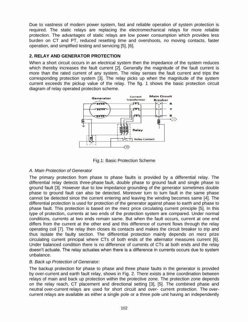
102
Due to vastness of modern power system, fast and reliable operation of system protection is
required. The static relays are replacing the electromechanical relays for more reliable
protection. The advantages of static relays are low power consumption which provides less
burden on CT and PT, reduced resetting time and overshoots, no moving contacts, faster
operation, and simplified testing and servicing [5], [6].
2. RELAY AND GENERATOR PROTECTION
When a short circuit occurs in an electrical system then the impedance of the system reduces which thereby increases the fault current [2]. Generally the magnitude of the fault current is more than the rated current of any system. The relay senses the fault current and trips the corresponding protection system [3]. The relay picks up when the magnitude of the system current exceeds the pickup value of the relay. The fig. 1 shows the basic protection circuit diagram of relay operated protection scheme.
Fig.1: Basic Protection Scheme
A. Main Protection of Generator
The primary protection from phase to phase faults is provided by a differential relay. The differential relay detects three-phase fault, double phase to ground fault and single phase to ground fault [3]. However due to low impedance grounding of the generator sometimes double phase to ground fault can also be detected. Moreover turn to turn fault in the same phase cannot be detected since the current entering and leaving the winding becomes same [4]. The differential protection is used for protection of the generator against phase to earth and phase to phase fault. This protection is based on the merz price circulating current principle [5]. In this type of protection, currents at two ends of the protection system are compared. Under normal conditions, currents at two ends remain same. But when the fault occurs, current at one end differs from the current at the other end and this difference of current flows through the relay operating coil [7]. The relay then closes its contacts and makes the circuit breaker to trip and thus isolate the faulty section. The differential protection mainly depends on merz prize circulating current principal where CTs of both ends of the alternator measures current [6]. Under balanced condition there is no difference of currents of CTs at both ends and the relay doesn’t actuate. The relay actuates when there is a difference in currents occurs due to system unbalance.
B. Back up Protection of Generator:
The backup protection for phase to phase and three phase faults in the generator is provided by over-current and earth fault relay, shows in Fig. 2. There exists a time coordination between relays of main and back up protection within the protective zone. The protection zone depends on the relay reach, CT placement and directional setting [3], [5]. The combined phase and neutral over-current relays are used for short circuit and over- current protection. The over-current relays are available as either a single pole or a three pole unit having an independently

103
adjustable current sensing circuit driving a common adjustable timing element. One of the main causes of ground fault insulation failure. The zero sequence impedance of a generator is usually lower than the positive or negative sequence and hence for a solidly grounded generator, the single phase to ground fault current is greater than the three phase fault current. To limit the ground fault current, generators are usually grounded through impedance. The high-sensitivity ground fault protection operates independently in order to detect ground fault since the ground fault current is relatively smaller than the phase fault current [4].
Fig. 2: Over current and earth fault protection of Alternator.
3. DESIGNED PROTECTION SCHEME AND ITS OPERATION
There are four blocks in the designed scheme. The block diagram of the designed protection scheme is shown in the fig. 3. The CTs (Current Transformer), bridge rectifiers, voltage regulator, capacitors and resistors are in the input section. The microcontroller is in the controlling section which compares the equivalent voltage of fault current with the reference value. The switching section has optocoupler, triac and resistor. The triac is operated according to the logical operation of microcontroller. The trip coil and dc battery is in the output section. The circuit breaker for alternator protection trips when the trip coil is energized due to operation of the triac.
Fig. 3: Block Diagram of the Design Protection Scheme
The complete circuit diagram of the protective system is shown in fig. 4. The fault current of the alternator is sensed by CT. For differential protection, the secondary windings of CTs are star connected. Since the microcontroller cannot sense current, therefore current is converted to equivalent voltage by using resistor. Similarly for over-current and earth fault protection, the fault current from CT is converted to equivalent voltage for logical operation of microcontroller. The resistors across CTs are selected in such a way that the fault current is converted to 5 V DC by using bridge rectifiers (BR1, BR2 and BR3) and capacitors.
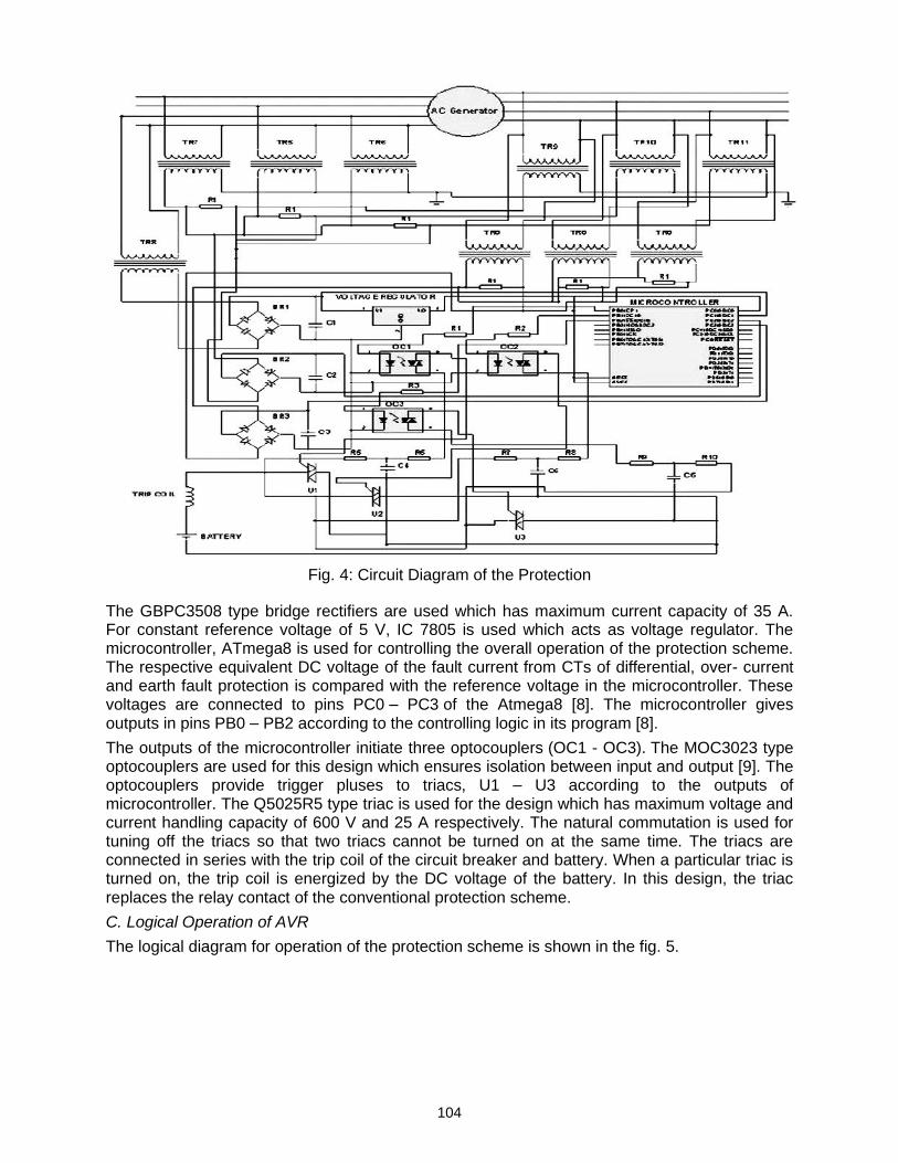
104
Fig. 4: Circuit Diagram of the Protection
The GBPC3508 type bridge rectifiers are used which has maximum current capacity of 35 A. For constant reference voltage of 5 V, IC 7805 is used which acts as voltage regulator. The microcontroller, ATmega8 is used for controlling the overall operation of the protection scheme. The respective equivalent DC voltage of the fault current from CTs of differential, over- current and earth fault protection is compared with the reference voltage in the microcontroller. These voltages are connected to pins PC0 – PC3 of the Atmega8 [8]. The microcontroller gives outputs in pins PB0 – PB2 according to the controlling logic in its program [8].
The outputs of the microcontroller initiate three optocouplers (OC1 - OC3). The MOC3023 type optocouplers are used for this design which ensures isolation between input and output [9]. The optocouplers provide trigger pluses to triacs, U1 – U3 according to the outputs of microcontroller. The Q5025R5 type triac is used for the design which has maximum voltage and current handling capacity of 600 V and 25 A respectively. The natural commutation is used for tuning off the triacs so that two triacs cannot be turned on at the same time. The triacs are connected in series with the trip coil of the circuit breaker and battery. When a particular triac is turned on, the trip coil is energized by the DC voltage of the battery. In this design, the triac replaces the relay contact of the conventional protection scheme.
C. Logical Operation of AVR
The logical diagram for operation of the protection scheme is shown in the fig. 5.
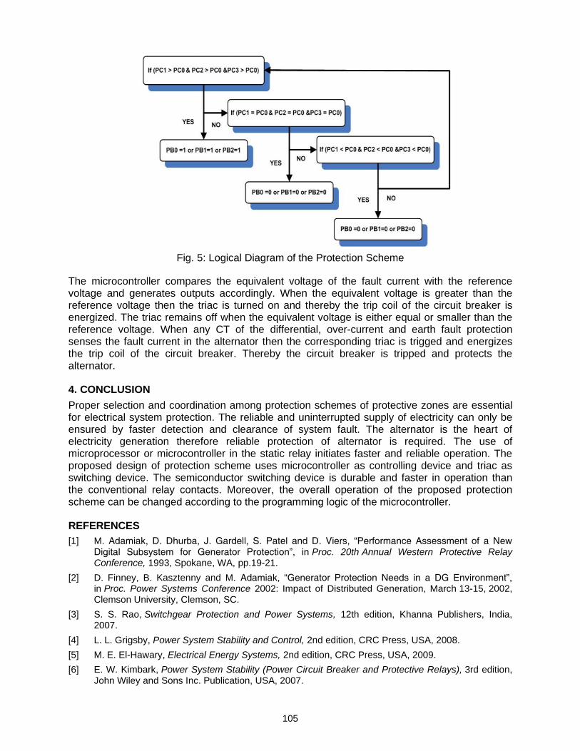
105
Fig. 5: Logical Diagram of the Protection Scheme
The microcontroller compares the equivalent voltage of the fault current with the reference voltage and generates outputs accordingly. When the equivalent voltage is greater than the reference voltage then the triac is turned on and thereby the trip coil of the circuit breaker is energized. The triac remains off when the equivalent voltage is either equal or smaller than the reference voltage. When any CT of the differential, over-current and earth fault protection senses the fault current in the alternator then the corresponding triac is trigged and energizes the trip coil of the circuit breaker. Thereby the circuit breaker is tripped and protects the alternator.
4. CONCLUSION
Proper selection and coordination among protection schemes of protective zones are essential for electrical system protection. The reliable and uninterrupted supply of electricity can only be ensured by faster detection and clearance of system fault. The alternator is the heart of electricity generation therefore reliable protection of alternator is required. The use of microprocessor or microcontroller in the static relay initiates faster and reliable operation. The proposed design of protection scheme uses microcontroller as controlling device and triac as switching device. The semiconductor switching device is durable and faster in operation than the conventional relay contacts. Moreover, the overall operation of the proposed protection scheme can be changed according to the programming logic of the microcontroller.
REFERENCES
[1] M. Adamiak, D. Dhurba, J. Gardell, S. Patel and D. Viers, “Performance Assessment of a New Digital Subsystem for Generator Protection”, in Proc. 20th Annual Western Protective Relay Conference, 1993, Spokane, WA, pp.19-21.
[2] D. Finney, B. Kasztenny and M. Adamiak, “Generator Protection Needs in a DG Environment”, in Proc. Power Systems Conference 2002: Impact of Distributed Generation, March 13-15, 2002, Clemson University, Clemson, SC.
[3] S. S. Rao, Switchgear Protection and Power Systems, 12th edition, Khanna Publishers, India, 2007.
[4] L. L. Grigsby, Power System Stability and Control, 2nd edition, CRC Press, USA, 2008.
[5] M. E. El-Hawary, Electrical Energy Systems, 2nd edition, CRC Press, USA, 2009.
[6] E. W. Kimbark, Power System Stability (Power Circuit Breaker and Protective Relays), 3rd edition, John Wiley and Sons Inc. Publication, USA, 2007.