Embed Size (px)
Citation preview

Basic Integrated Circuit Processing
ELEC 3908, Physical Electronics, Lecture 4
David J. Walkey ELEC 3908, Physical Electronics: Basic IC Processing (4) Page 2
Lecture Outline
• Details of the physical structure of devices will be very important in developing models for electrical behavior
• Device structure is better understood by following through fabrication sequence
• The basic processing steps used in fabricating integrated devices will be examined in this lecture, then the use of these process steps in fabricating a diode, bipolar junction transistor or FET will be dealt with in later lectures
David J. Walkey ELEC 3908, Physical Electronics: Basic IC Processing (4) Page 3
Ingot Growth• First step in production of an
integrated circuit is growth of a large piece of almost perfectly crystalline semiconductingmaterial called an ingot (boule)
• Small seed crystal is suspended in molten material then pulled (1m/hr) and rotated (1/2 rps) to form the ingot
• Result is an ingot approx. 1m long and anywhere from 75 to 300 mm in diameter
• Dopant is almost always added to the molten material
David J. Walkey ELEC 3908, Physical Electronics: Basic IC Processing (4) Page 4
Ingot Growth
David J. Walkey ELEC 3908, Physical Electronics: Basic IC Processing (4) Page 5
Wafer Sawing
• Ingots are then sawed into wafers approximately 500-1000 m (0.5 to 1 mm) thick using a diamond tipped saw
• Wafers are the starting material for integrated circuit manufacture, and are normally referred to as the substrate
• Surface of the wafer is smoothed with combination of chemical and mechanical polishing steps
David J. Walkey ELEC 3908, Physical Electronics: Basic IC Processing (4) Page 6
Photolithography
• Lithography refers to the transfer of an image onto paper using a plate and ink-soluble grease
• Photolithography is the transfer of an image using photographic techniques
• Photolithography transfers designer generated information (device placement and interconnections) to an actual ICstructure using masks which contain the geometrical information
• The process of photolithography is repeated many times in manufacture of an IC to build up device structures and interconnections

David J. Walkey ELEC 3908, Physical Electronics: Basic IC Processing (4) Page 7
Photolithography - Application of Photoresist• First step in photolithography is
to coat the surface with approx 1 m of photoresist (PR)
• PR will be the medium whereby the required image is transferred to the surface
• PR is often applied to the center of the wafer, which is then spun to force the PR over the entire surface
• Note that the scale of these diagrams is not correct - the PR is approx. 1 m thick while the wafer is 1000 m thick.
David J. Walkey ELEC 3908, Physical Electronics: Basic IC Processing (4) Page 8
Photolithography - Exposure• The PR is then exposed to UV
(ultraviolet) radiation through a mask
• The masks generated from information about device placement and connection
• The UV radiation causes a chemical change in the PR
• The transfer of information from the mask to the surface occurs through the UV-induced chemical change - only occurs where the mask is transparent
wafer
mask mask
UV radiation
David J. Walkey ELEC 3908, Physical Electronics: Basic IC Processing (4) Page 9
Photolithography - Development• The PR is then developed using
a chemical developer• Two possibilities:
– A negative PR is hardened against the developer by the UV radiation, and hence remains on the surface where UV shone through the mask
– A positive PR is the opposite, it is removed where the UV shone through the mask
• Assume a negative PR for this example, so the PR on the sides will be weakened and removed by the developer
David J. Walkey ELEC 3908, Physical Electronics: Basic IC Processing (4) Page 10
Photolithography - Final Structure• Once the developer has been
washed off, the result is PR in the region corresponding to the transparent part of the mask(the mask is shown again to indicate where the final region is formed – it is not part of the final structure)
• Subsequent processing steps will use this structure to form device areas, interconnects, etc.
• Note that an optically reversed mask and a positive resist would give the same structure
wafer
selected area
mask mask(mask shown to indicate final region)
David J. Walkey ELEC 3908, Physical Electronics: Basic IC Processing (4) Page 11
Mask Generation - Reticle• The geometry information over
the entire IC required for a particular photolithography step is used to create a reticle, a 10X sized optical plate
• There can be anywhere from 6 to 24+ individual photolithography steps in a manufacturing process, each with its own set of geometrical information captured in a reticle
David J. Walkey ELEC 3908, Physical Electronics: Basic IC Processing (4) Page 12
Mask Generation - Step and Repeat• In order to fabricate many devices simultaneously, the reticle
information is reduced and projected many times onto a 1X mask usinga step and repeat process

David J. Walkey ELEC 3908, Physical Electronics: Basic IC Processing (4) Page 13
Mask Generation - Final 1X Mask• The 1X mask which results
from the step and repeat process contains all the information for a particular photolith step for all chips which will be fabricated on the wafer
• This image is projected during the exposure step to cause PR chemical changes in the appropriate locations
David J. Walkey ELEC 3908, Physical Electronics: Basic IC Processing (4) Page 14
Reticle and Mask Example
4:1 Reticle1:1 Mask
David J. Walkey ELEC 3908, Physical Electronics: Basic IC Processing (4) Page 15
Example Simple Mask Set
• Shown below is a highly simplified layout for a two transistor digital gate, and the masks which would be required based on its layout (see MOSFET)
• Not in notes, just shown as an example of how masks are derived from a user-generated layout
layout (4 layers) layer 1 mask layer 2 mask layer 3 mask layer 4 mask
David J. Walkey ELEC 3908, Physical Electronics: Basic IC Processing (4) Page 16
Etching - Dry and Wet Processes• Etching is the selective removal
of material from the chip surface
• In dry etching, ions of a neutral material are accelerated toward the surface and cause ejection of atoms of all materials
• In wet etching, a chemical etchant is used to remove material via a chemical reaction
David J. Walkey ELEC 3908, Physical Electronics: Basic IC Processing (4) Page 17
Etching - Selectivity and Anisotropy• Two most important issues in etching are selectivity and anisotropy
– Selectivity refers to the ability of an etchant to remove one material on the surface while leaving another intact.
– Isotropic refers to the tendency of the etching to proceed laterally as well as downward
David J. Walkey ELEC 3908, Physical Electronics: Basic IC Processing (4) Page 18
Thermal Oxidation - Oxidation Furnace• One of the simplest steps in IC processing is thermal oxidation, the
growth of a layer of silicon dioxide (SiO2) on the substrate surface• Requires only substrate heating to 900-1200 C in a dry (O2) or wet
(H20 steam) ambient using an oxidation furnace• Silicon oxidizes quite readily - one reason why Si is so widely used

David J. Walkey ELEC 3908, Physical Electronics: Basic IC Processing (4) Page 19
Oxidation – Boat/Tube Examples
David J. Walkey ELEC 3908, Physical Electronics: Basic IC Processing (4) Page 20
Oxidation - System
David J. Walkey ELEC 3908, Physical Electronics: Basic IC Processing (4) Page 21
Thermal Oxidation - Oxide Formation• Oxide forms due to the
chemical reaction between oxygen in the ambient and silicon in the substrate
• Substrate silicon is consumed during the reaction, so oxide layer grows in both directions from the original substrate surface (approx. 50/50)
David J. Walkey ELEC 3908, Physical Electronics: Basic IC Processing (4) Page 22
Thermal Oxidation - Wet vs. Dry Rates• Due to the different reaction
mechanisms, oxidation in a wet ambient is many times faster than oxidation in a dry ambient
• However, the oxide quality is much better when a dry ambient is used
• Thick isolation layers are therefore formed using wet oxidation, while MOSFET gate oxides are formed with dry oxidation
David J. Walkey ELEC 3908, Physical Electronics: Basic IC Processing (4) Page 23
Local Oxidation• The presence of another
material such as silicon nitride (Si3N4) on the surface inhibits the growth of oxide in that region
• This allows selective or localoxidation of the substrate surface - will be used to isolate devices or conductive layers
• Some oxidation does occur laterally under the nitride layer, giving rise to the bird’s beak effect
David J. Walkey ELEC 3908, Physical Electronics: Basic IC Processing (4) Page 24
Dopant Diffusion• Dopant can be introduced into
the substrate through diffusion• Diffusion is a general physical
process which drives particles down a concentration gradient
• The substrate is heated in the presence of dopant atoms, which then diffuse into the substrate
• Diffusion may also occur into other layers which are present such as silicon dioxide
• Large amount of lateraldiffusion also occurs

David J. Walkey ELEC 3908, Physical Electronics: Basic IC Processing (4) Page 25
Ion Implantation• In ion implantation, dopant
atoms are accelerated toward the substrate surface and enter due to their kinetic energy
• This is the preferred technique for introduction of dopantatoms since the amount of lateral diffusion is much lower
David J. Walkey ELEC 3908, Physical Electronics: Basic IC Processing (4) Page 26
Ion Implantation System
Ion source
Analyzing magnetAcceleration columnIon beam
Plasma
Processchamber
Extraction assembly
Scanningdisk
David J. Walkey ELEC 3908, Physical Electronics: Basic IC Processing (4) Page 27
Ion Implantation - Predep and Drive-in• Ion implantation can be
used to form a deep region of doping using a two step procedure
– A high concentration of dopant is deposited near the surface in the predeposition or predepstage
– The dopant source is then removed and the wafer heated to cause redistribution of the dopant via diffusion in the drive-in stage
David J. Walkey ELEC 3908, Physical Electronics: Basic IC Processing (4) Page 28
Deposition
• Layers of materials such as metal (and in some cases silicon dioxide) may need to be formed on the surface
• General procedure of forming a layer of material on the surface is termed deposition
• Two types can be identified, physical and chemical– In physical deposition, a piece (target) of the material to be
deposited is bombarded with ions, ejecting atoms of material which then adhere to the substrate surface
– Chemical deposition uses an ongoing chemical reaction to form the desired material as a precipitate on the substrate surface
• A specialized form of deposition is epitaxy, the formation of a layer of crystalline semiconductor material
David J. Walkey ELEC 3908, Physical Electronics: Basic IC Processing (4) Page 29
Sputtering System
David J. Walkey ELEC 3908, Physical Electronics: Basic IC Processing (4) Page 30
Patterning
• The use of a series of PR deposition, exposure, development and etching to create regions of particular shape is called patterning
• For example, if a newly deposited metal layer was coated with PR, exposed using a mask, developed and etched using a method which selectively removed the metal not covered by the PR, this would be referred to as “patterning” the metal
• There will be many individual patterning steps in the creation of a useful integrated structure
David J. Walkey ELEC 3908, Physical Electronics: Basic IC Processing (4) Page 31
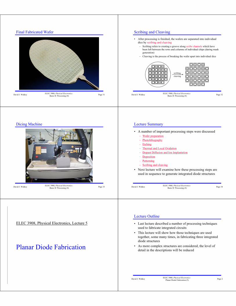
Final Fabricated Wafer
David J. Walkey ELEC 3908, Physical Electronics: Basic IC Processing (4) Page 32
Scribing and Cleaving• After processing is finished, the wafers are separated into individual
dice by scribing and cleaving– Scribing refers to creating a groove along scribe channels which have
been left between the rows and columns of individual chips (during mask generation)
– Cleaving is the process of breaking the wafer apart into individual dice
David J. Walkey ELEC 3908, Physical Electronics: Basic IC Processing (4) Page 33
Dicing Machine
David J. Walkey ELEC 3908, Physical Electronics: Basic IC Processing (4) Page 34
Lecture Summary
• A number of important processing steps were discussed– Wafer preparation– Photolithography– Etching– Thermal and Local Oxidation– Dopant Diffusion and Ion Implantation– Deposition– Patterning– Scribing and cleaving
• Next lecture will examine how these processing steps are used in sequence to generate integrated diode structures
Planar Diode Fabrication
ELEC 3908, Physical Electronics, Lecture 5
David J. Walkey ELEC 3908, Physical Electronics: Planar Diode Fabrication (5) Page 2
Lecture Outline
• Last lecture described a number of processing techniques used to fabricate integrated circuits
• This lecture will show how those techniques are used together, some many times, in fabricating three integrated diode structures
• As more complex structures are considered, the level of detail in the descriptions will be reduced

David J. Walkey ELEC 3908, Physical Electronics: Planar Diode Fabrication (5) Page 3
Diode Types Considered
• Fabrication of three types of diodes examined:– Substrate Diode: simple pn-junction fabricated from a single
counterdoped region in the substrate– Well Diode: slightly more complicated structure with a deeper
region of counter doping and a highly doped diffusion– Epitaxial Diode: More complicated processing using an epitaxial
layer, but offers the best performance
David J. Walkey ELEC 3908, Physical Electronics: Planar Diode Fabrication (5) Page 4
Substrate Diode - Nitride Protection• First step is to deposit a layer of silicon nitride (Si3N4) over the wafer
surface• Would normally be done using chemical vapor deposition (CVD)
David J. Walkey ELEC 3908, Physical Electronics: Planar Diode Fabrication (5) Page 5
Substrate Diode - Photoresist Coating• Surface (top of nitride layer) then coated with photoresist (PR)
David J. Walkey ELEC 3908, Physical Electronics: Planar Diode Fabrication (5) Page 6
Substrate Diode - Exposure• Surface of PR is then exposed to UV radiation through a mask created
from geometry information supplied by the designer
David J. Walkey ELEC 3908, Physical Electronics: Planar Diode Fabrication (5) Page 7
Substrate Diode - Development of Photoresist• Photoresist is then developed chemically• A negative photoresist remains where it was exposed to UV
David J. Walkey ELEC 3908, Physical Electronics: Planar Diode Fabrication (5) Page 8
Substrate Diode - Etching of Nitride• The nitride layer is then etched chemically• Only the nitride areas where photoresist was removed will be etched

David J. Walkey ELEC 3908, Physical Electronics: Planar Diode Fabrication (5) Page 9
Substrate Diode - Finished Nitride Etch• When the nitride etching is complete, all of the nitride layer outside the
remaining area of photoresist has been removed• Both nitride and photoresist remain in the exposed area
David J. Walkey ELEC 3908, Physical Electronics: Planar Diode Fabrication (5) Page 10
Substrate Diode - Photoresist Removal• The photoresist still covering the remaining nitride area is now
removed
David J. Walkey ELEC 3908, Physical Electronics: Planar Diode Fabrication (5) Page 11
Substrate Diode - Thermal Oxidation• A layer of silicon dioxide is grown using thermal oxidation • The oxide is prevented from growing in the area covered by silicon
nitride - this is the purpose of the nitride layer
David J. Walkey ELEC 3908, Physical Electronics: Planar Diode Fabrication (5) Page 12
Substrate Diode - Nitride Removal• When oxidation is complete, the nitride layer is removed• The result is a structure with thick isolation oxide everywhere except
the areas which will become the active diode
David J. Walkey ELEC 3908, Physical Electronics: Planar Diode Fabrication (5) Page 13
Substrate Diode - Implantation• An implantation (ion implantation or diffusion) is now done to create a
counterdoped region which will form one side of the pn-junction• The oxide absorbs the dopant outside of the active area, preventing
dopant from penetrating into the substrate anywhere but the active area
David J. Walkey ELEC 3908, Physical Electronics: Planar Diode Fabrication (5) Page 14
Substrate Diode - Surface Metal Patterning• Metal is now deposited over the entire wafer surface• Another series of patterning steps is used, along with another mask, to
remove metal everywhere except the contact to the diode and wherever else the connection is made

David J. Walkey ELEC 3908, Physical Electronics: Planar Diode Fabrication (5) Page 15
Substrate Diode - Substrate Connection• Metal is deposited on the backside of the wafer to form the other
connection• Note that all substrate diodes share a common (substrate) connection
David J. Walkey ELEC 3908, Physical Electronics: Planar Diode Fabrication (5) Page 16
Well Diode
• Two problems with the substrate diode:– Current flows through the entire thickness of the substrate (500 -
1000 m) to reach the back contact– Substrate is common for all diodes on the chip, diodes all have a
common connection
• Better solution is to use a well diode, which is formed in a region of opposite doping (counterdoped) to the substrate, and a heavily doped region of the same type as the substrate
• Eliminates long current path through the substrate, and allows two independent terminals, since well is isolated from the substrate
David J. Walkey ELEC 3908, Physical Electronics: Planar Diode Fabrication (5) Page 17
Well Diode - Nitride Deposition, Thermal Oxidation• A layer of nitride is deposited and patterned so that it exists on where
the active area (including the well) is to be formed• Thermal oxidation used to form an oxide layer
David J. Walkey ELEC 3908, Physical Electronics: Planar Diode Fabrication (5) Page 18
Well Diode - Well implant• A deep implantation is done to create the well - a counterdoped region
which will be one side of the diode
David J. Walkey ELEC 3908, Physical Electronics: Planar Diode Fabrication (5) Page 19
Well Diode - Well Contact Implant• To connect to the well, a highly doped region of the same type as the
well is created• All the usual patterning steps are used (PR deposition, exposure with
mask, development, removal of PR)
David J. Walkey ELEC 3908, Physical Electronics: Planar Diode Fabrication (5) Page 20
Well Diode - Diode Diffusion• The other side of the pn-junction structure is formed with a heavy
implant into the well

David J. Walkey ELEC 3908, Physical Electronics: Planar Diode Fabrication (5) Page 21
Well Diode - Isolation Oxide• A layer of silicon dioxide is deposited on the surface (thermal
oxidation would grow into the existing diffusion structure)• This layer is required because the two contacts to the diode are both at
the surface, hence an isolation layer is required to prevent shorting
David J. Walkey ELEC 3908, Physical Electronics: Planar Diode Fabrication (5) Page 22
Well Diode - Contact Cuts and Metallization• Contact cuts are etched through the isolation oxide to the diffusions
using a full series of patterning steps• Metal is deposited on the surface and patterned for interconnections• Provided the well to substrate junction is reverse biased, the well diode
is isolated from the substrate, and hence from other devices
David J. Walkey ELEC 3908, Physical Electronics: Planar Diode Fabrication (5) Page 23
Epitaxial Diode
• Well diode is an improvement over the substrate diode, but current flow is lateral so the exact performance is hard to predict
• Best solution, but with corresponding process complexity, is the epitaxial diode, fabricated on an epitaxial layer of silicon
David J. Walkey ELEC 3908, Physical Electronics: Planar Diode Fabrication (5) Page 24
Epitaxial Diode - Thermal Oxidation• Starting material is a lightly doped substrate, assume p- for this
example• Layer of oxide grown using thermal oxidation step
David J. Walkey ELEC 3908, Physical Electronics: Planar Diode Fabrication (5) Page 25
Epitaxial Diode - Buried Layer Formation• Using a photolithography step (and an associated mask) a window is
formed in the oxide and a heavy n-type implant performed to create a highly doped n-type (n+) region called the buried layer
• The oxide is then removed using a selective etching step• The result is a heavy n+ doping which will form the back connection to
the diode
David J. Walkey ELEC 3908, Physical Electronics: Planar Diode Fabrication (5) Page 26
Epitaxial Diode - Epitaxial Deposition• The next step is to use epitaxy to deposit a layer of high quality
crystalline silicon called the epi layer on the wafer surface• Some diffusion of dopant from the n+ region occurs into the epi layer• Another series of photolithography steps is used to form a masking
oxide over the region which will become the active diode area

David J. Walkey ELEC 3908, Physical Electronics: Planar Diode Fabrication (5) Page 27
Epitaxial Diode - Isolation Implants• A heavy p-type (p+) implant is then used to form regions extending
right through the epi and into the substrate (lateral diffusion also results in extension under masking oxide)
• These isolation regions electrically isolate the device from all others fabricated in the epi layer
David J. Walkey ELEC 3908, Physical Electronics: Planar Diode Fabrication (5) Page 28
Epitaxial Diode - n+ and p+ Implants• Oxide is deposited and patterned to open a window for an n+ doping
which will form a contact through the n-type epi layer down to the buried layer
• Oxide is again deposited and patterned to produce an opening for a heavy p-type implant which will form the other side of the pn-junctionwith the epi layer
David J. Walkey ELEC 3908, Physical Electronics: Planar Diode Fabrication (5) Page 29
Epi Diode - Metallization• Another layer of oxide is deposited to isolate the metal connections
from the epi and isolation p+ implants• Openings are patterned to allow contact to the p+ diode diffusion and
the n+ epi contact diffusion• Metal is deposited and patterned to form connections to the diode
David J. Walkey ELEC 3908, Physical Electronics: Planar Diode Fabrication (5) Page 30
Epitaxial Diode - Current Flow• The active diode area is only a small portion of the epitaxial structure• Current flow in the epi diode is through the active area, along the
buried layer and up and out the n+ contact diffusion• Benefit is well controlled current flow path• Also forms a major portion of the structure of an integrated BJT
David J. Walkey ELEC 3908, Physical Electronics: Planar Diode Fabrication (5) Page 31
Summary of Diode Structures
• Three diode structures examined– Substrate: simple, but poor performance– Well: better, and getting more complicated– Epi: best, but most complicated
lightly doped substratep-
p+ p+n+p+
n+ buried layer
n- epitaxial layer
p-substrate
n-well
p+n+
Al
substrate thickness not to scale
David J. Walkey ELEC 3908, Physical Electronics: Planar Diode Fabrication (5) Page 32
Lecture Summary
• The use of the basic processing techniques from lecture 4 in creating three diode structures was discussed
• Note that many of the techniques are performed over and over as successive features are created
• The substrate diode is simple but suffers from at least one disadvantage – all substrate diodes have one terminal connected together
• The well diode is an improvement, but has primarily lateral flow, which can be difficult to characterize
• The epi diode gives the best performance, but is much more complex to fabricate than the first two

BJT Structure and Fabrication
ELEC 3908, Physical Electronics, Lecture 15
David J. Walkey ELEC 3908, Physical Electronics: BJT Structure and Fabrication (15) Page 2
Lecture Outline
• Now move on to bipolar junction transistor (BJT)• Strategy for next few lectures similar to diode: structure
and processing, basic operation, basic quantitative modeling, more advanced features
• This lecture begins by looking at the structure and processing of the double diffused planar structure, very similar to epi-diode as well as layout from point of view of ASIC designer
• Then consider basic current flow in structure, 1D approximation and nomenclature
• Calculate depletion widths for junctions
David J. Walkey ELEC 3908, Physical Electronics: BJT Structure and Fabrication (15) Page 3
Fabrication of Double-Diffused BJT Structure
• Examine fabrication steps to create a vertical npn double-diffused BJT structure on an epitaxial layer
• Similar structure to the epi diode• Name derived from the fact that the base and emitter are
formed by implants - in a more modern device the emitter would be formed by another method
• Show more detail here than in notes and one small variation - separate sinker and emitter diffusion steps
David J. Walkey ELEC 3908, Physical Electronics: BJT Structure and Fabrication (15) Page 4
BJT Fabrication - Starting Material• The starting material for a vertical npn structure is p-type substrate
doped at 1016 /cm3 or less
David J. Walkey ELEC 3908, Physical Electronics: BJT Structure and Fabrication (15) Page 5
BJT Fabrication - First Oxide Deposition• Using a chemical process (CVD), oxide is deposited on the wafer
surface
David J. Walkey ELEC 3908, Physical Electronics: BJT Structure and Fabrication (15) Page 6
BJT Fabrication - Patterning of First Oxide• Photoresist spun on top of the oxide is exposed using the buried layer
mask (mask #1)• The BL mask is usually generated automatically from other masks

David J. Walkey ELEC 3908, Physical Electronics: BJT Structure and Fabrication (15) Page 7
BJT Fabrication - Etching of First Oxide• Using a wet etch, a window corresponding to the buried layer mask is
opened in the oxide
David J. Walkey ELEC 3908, Physical Electronics: BJT Structure and Fabrication (15) Page 8
BJT Fabrication - Final Buried Layer Window• After the remaining PR is stripped, the deposited oxide has an opening
etched in the location specified by the buried layer mask
David J. Walkey ELEC 3908, Physical Electronics: BJT Structure and Fabrication (15) Page 9
BJT Fabrication - Buried Layer Implant• The buried layer is formed with a high density (dose) implant of n-type
dopant, usually Phosphorous• Some lateral diffusion of dopants takes place during the implant• Dopant is also introduced into the masking oxide
David J. Walkey ELEC 3908, Physical Electronics: BJT Structure and Fabrication (15) Page 10
BJT Fabrication - Final Buried Layer• After the masking oxide is removed (etched), the result is a highly
doped buried layer region in the original silicon substrate
David J. Walkey ELEC 3908, Physical Electronics: BJT Structure and Fabrication (15) Page 11
BJT Fabrication - Deposition of Epi Layer• Using epitaxial deposition (similar to CVD), a layer of very high
quality (crystalline) silicon is deposited on the surface• Some diffusion of dopants occurs from the highly doped buried layer
into the more lightly doped epitaxial layer
David J. Walkey ELEC 3908, Physical Electronics: BJT Structure and Fabrication (15) Page 12
BJT Fabrication - Final Epi Layer• The resulting epitaxial layer will form the collector region in the BJT,
with the highly doped (low R) buried layer forming an equipotentialregion under the device
• Note that the buried layer is now completely enclosed in siliconmaterial
David J. Walkey ELEC 3908, Physical Electronics: BJT Structure and Fabrication (15) Page 13
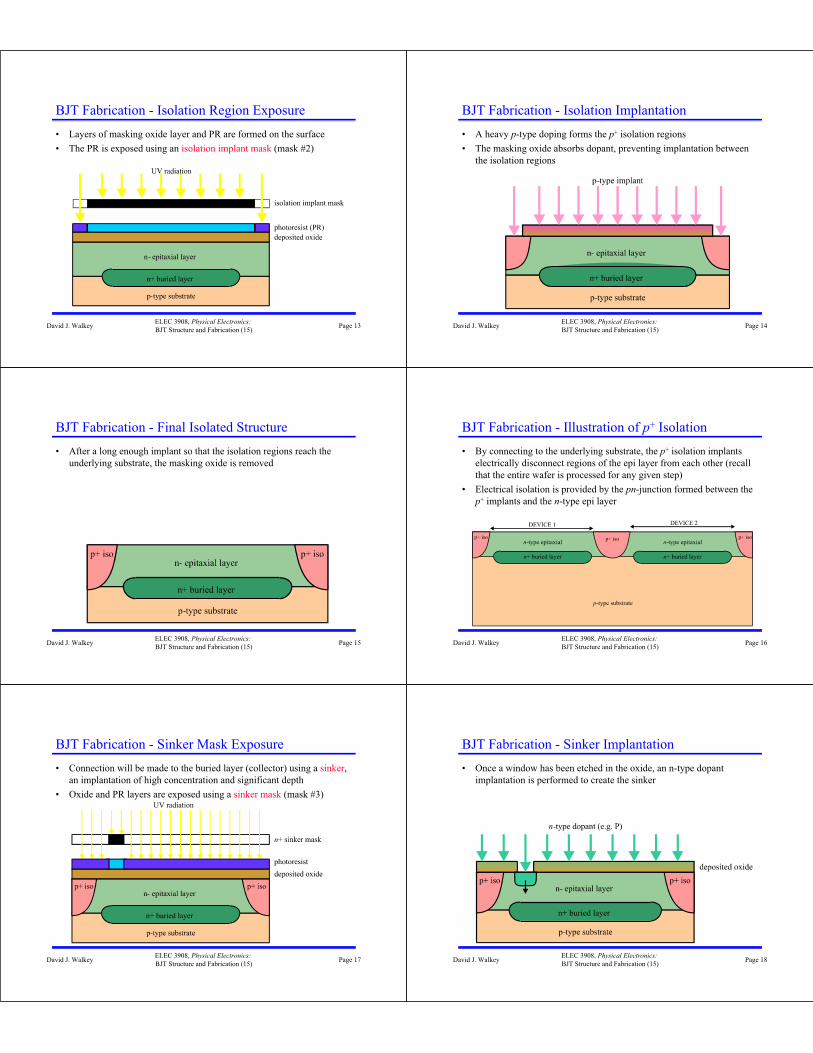
BJT Fabrication - Isolation Region Exposure• Layers of masking oxide layer and PR are formed on the surface• The PR is exposed using an isolation implant mask (mask #2)
David J. Walkey ELEC 3908, Physical Electronics: BJT Structure and Fabrication (15) Page 14
BJT Fabrication - Isolation Implantation• A heavy p-type doping forms the p+ isolation regions• The masking oxide absorbs dopant, preventing implantation between
the isolation regions
David J. Walkey ELEC 3908, Physical Electronics: BJT Structure and Fabrication (15) Page 15
BJT Fabrication - Final Isolated Structure• After a long enough implant so that the isolation regions reach the
underlying substrate, the masking oxide is removed
David J. Walkey ELEC 3908, Physical Electronics: BJT Structure and Fabrication (15) Page 16
BJT Fabrication - Illustration of p+ Isolation• By connecting to the underlying substrate, the p+ isolation implants
electrically disconnect regions of the epi layer from each other (recall that the entire wafer is processed for any given step)
• Electrical isolation is provided by the pn-junction formed between the p+ implants and the n-type epi layer
David J. Walkey ELEC 3908, Physical Electronics: BJT Structure and Fabrication (15) Page 17
BJT Fabrication - Sinker Mask Exposure• Connection will be made to the buried layer (collector) using a sinker,
an implantation of high concentration and significant depth• Oxide and PR layers are exposed using a sinker mask (mask #3)
David J. Walkey ELEC 3908, Physical Electronics: BJT Structure and Fabrication (15) Page 18
BJT Fabrication - Sinker Implantation• Once a window has been etched in the oxide, an n-type dopant
implantation is performed to create the sinker

David J. Walkey ELEC 3908, Physical Electronics: BJT Structure and Fabrication (15) Page 19
BJT Fabrication - Final Sinker Structure• Depending on the implantation conditions and the thickness of the epi
region, the sinker may or may not reach right down to the buried layer
David J. Walkey ELEC 3908, Physical Electronics: BJT Structure and Fabrication (15) Page 20
BJT Fabrication - Base Mask Exposure• Oxide/PR are formed on the surface, and the region which will form
the active base is exposed using the base mask (mask #4)
David J. Walkey ELEC 3908, Physical Electronics: BJT Structure and Fabrication (15) Page 21
BJT Fabrication - Base Region Implantation• A p-type dopant (usually Boron) is implanted into the epi layer through
the oxide window to form the p-type base region
David J. Walkey ELEC 3908, Physical Electronics: BJT Structure and Fabrication (15) Page 22
BJT Fabrication - Final Base Region• After implantation is complete, a p-type counterdoped base region has
been formed in the n-type collector epi
David J. Walkey ELEC 3908, Physical Electronics: BJT Structure and Fabrication (15) Page 23
BJT Fabrication - Emitter Region Exposure• Oxide/PR layers are exposed using an emitter mask (mask #5)
David J. Walkey ELEC 3908, Physical Electronics: BJT Structure and Fabrication (15) Page 24
BJT Fabrication - Emitter Implant• A heavy n-type dopant (usually As) is implanted through the oxide
window opening to form the emitter• Control of this implant is critical to the BJT’s operation

David J. Walkey ELEC 3908, Physical Electronics: BJT Structure and Fabrication (15) Page 25
BJT Fabrication - Final Emitter Structure• With the creation of the n+ emitter region in the p-base (in the n-epi
collector), the basic BJT structure is complete, only metal contacts remain
David J. Walkey ELEC 3908, Physical Electronics: BJT Structure and Fabrication (15) Page 26
BJT Fabrication - Contact Cut Exposure• Oxide is deposited which will isolate metal connections• PR is exposed using contact cut mask (mask #6)
David J. Walkey ELEC 3908, Physical Electronics: BJT Structure and Fabrication (15) Page 27
BJT Fabrication - Contact Window Etching• Etching of contact openings requires selectivity so etching does not
remove emitter, therefore wet etchant used
David J. Walkey ELEC 3908, Physical Electronics: BJT Structure and Fabrication (15) Page 28
BJT Fabrication - Final Contact Cuts• After etching, openings have been created in the oxide which will
allow access to the collector sinker, base and emitter regions
David J. Walkey ELEC 3908, Physical Electronics: BJT Structure and Fabrication (15) Page 29
BJT Fabrication - Metal Deposition and Exposure• After metal is deposited and PR formed on surface, exposure is
performed using a metal mask (mask #7)
David J. Walkey ELEC 3908, Physical Electronics: BJT Structure and Fabrication (15) Page 30
BJT Fabrication - Final Interconnect Structure• Once the metal has been etched to form interconnections between
contacts, the structure is complete• Most modern processes would use more than one level of metal

David J. Walkey ELEC 3908, Physical Electronics: BJT Structure and Fabrication (15) Page 31
BJT Layout - Single Emitter, Base and Collector• Top view layout shows
the various masks used to realize the basic structure
• Cross section is duplicated to show correspondence
• Buried layer and isolation masks can by generated automatically based on size of base region and position of collector
David J. Walkey ELEC 3908, Physical Electronics: BJT Structure and Fabrication (15) Page 32
BJT Layout - Multiple base contacts • Many other devices possible - example shows single emitter and
collector with two base contacts• Large current devices have many interdigitated emitter and base
regions
David J. Walkey ELEC 3908, Physical Electronics: BJT Structure and Fabrication (15) Page 33
Current Flow in the Integrated npn BJT• In the integrated BJT structure, the principle current flow for normal
operation is through the sinker, buried layer and up through the vertical npn structure
• The actual active area of the device is a relatively small portion of the overall structure
David J. Walkey ELEC 3908, Physical Electronics: BJT Structure and Fabrication (15) Page 34
BJT 1D Approximation• For initial analysis, isolate the
active region between the emitter and buried layer and assume 1D operation as in diode, with uniform doping approximations
• Neglects collector resistances associated with sinker and buried layer and base resistance associated with external regions, but can add those later
• Use 1D area given by product of emitter width and length
A b lE E E
David J. Walkey ELEC 3908, Physical Electronics: BJT Structure and Fabrication (15) Page 35
BJT Nomenclature
Quantity Emitter Base Collector UnitsDoping NDE NAB NDC /cm3
MinorityConcentration
pEo nBo pCo /cm3
DiffusionCoefficient
DpE DnB DpC cm2/sec
David J. Walkey ELEC 3908, Physical Electronics: BJT Structure and Fabrication (15) Page 36
BJT Width Definitions• An npn BJT has two pn-junctions, and hence two depletion regions• Label the widths of the base-emitter and base-collector depletion
regions WBE and WBC, respectively• Widths of remaining neutral region in collector, base and emitter are
WC, WB and WE, respectively

David J. Walkey ELEC 3908, Physical Electronics: BJT Structure and Fabrication (15) Page 37
BJT Depletion Widths
• Each depletion width is calculated using the previous pn-junction expression with the appropriate built in potential
VkTq
N NnbiBE
AB DE
iln 2 V
kTq
N NnbiBC
AB DC
iln 2
Wq N N
V VBESi
AB DEbiBE BE
2 1 1
Wq N N
V VBCSi
AB DCbiBC BC
2 1 1
David J. Walkey ELEC 3908, Physical Electronics: BJT Structure and Fabrication (15) Page 38
Example 15.1: BJT Width Calculations• Calculate the equilibrium minority concentrations, diffusion
coefficients and the widths of the collector, base and emitter neutral regions for the structure given below at the biases shown.
David J. Walkey ELEC 3908, Physical Electronics: BJT Structure and Fabrication (15) Page 39
Example 15.1: Solution
• Using the values of doping given and the applied potentials (note that VBC is calculated from VCE and VBE as 0.8 - 1.5 = -0.7V)
VbiBE 0 02610 10
145 100 93
17 19
10 2. ln.
. V
WBE2 117 8 854 10
16 101
101
100 93 0 8 4 2 10
14
19 17 196. .
.. . . cm
VbiBC 0 02610 5 10145 10
0 7417 15
10 2. ln.
. V
WBC2 117 8 854 10
16 101
101
5 100 74 0 7 6 3 10
14
19 17 155. .
.. . . cm
David J. Walkey ELEC 3908, Physical Electronics: BJT Structure and Fabrication (15) Page 40
Example 15.1: Solution (con’t)
• The collector neutral width is the collector material width minus the extent of the BC depletion region into the collector
W WN
N NC BCAB
AB DC4 10
4 10 6 3 1010
10 5 10
3 4 10
4
4 517
17 15
4
.
. cm
David J. Walkey ELEC 3908, Physical Electronics: BJT Structure and Fabrication (15) Page 41
Example 15.1: Solution (con’t)
• The emitter neutral width is the emitter material width minus the extent of the BE depletion region into the emitter (note emittermaterial width)
W WN
N NE BEAB
AB DE1 10
4 10 4 2 1010
10 10
1 10
4
4 617
17 19
4
.
cm
David J. Walkey ELEC 3908, Physical Electronics: BJT Structure and Fabrication (15) Page 42
Example 15.1: Solution (con’t)
• The base neutral width is the base material width minus the extents of the BE and BC depletion regions into the base
W WN
N NW
NN NB BE
DE
DE ABBC
DC
DC AB15 10
15 10 4 2 1010
10 106 3 10
5 105 10 10
14 10
4
4 619
19 175
15
15 17
4
.
. . .
. cm

David J. Walkey ELEC 3908, Physical Electronics: BJT Structure and Fabrication (15) Page 43
Example 15.1: Solution (con’t)
• The equilibrium densities and diffusion coefficients are given by standard formulas
pn
N
nn
N
pn
N
D DkTq
DkTq
Eoi
DE
Boi
AB
Coi
DC
pE pC p
nB n
2 10 2
19
2 10 2
173
2 10 2
154
145 1010
21
145 1010
21 10
145 105 10
4 2 10
12 2
34 9
.
..
..
.
.
/ cm
/ cm
/ cm
cm sec
cm sec
3
3
3
2
2
David J. Walkey ELEC 3908, Physical Electronics: BJT Structure and Fabrication (15) Page 44
Lecture Summary
• Looked in detail at fabrication of double diffused structure• Current flow path illustrates importance of conductive epi
buried layer• 1D approximation uses emitter area AE
• Three regions require slightly more complex naming scheme for dopings, etc.
• Depletion widths calculated – based on pn junction equation applied to each junction
• Base neutral width is region of base not accounted for by depletion regions
MOSFET Structure and Processing
ELEC 3908, Physical Electronics, Lecture 20
David J. Walkey ELEC 3908, Physical Electronics: MOSFET Structure and Processing (20) Page 2
Lecture Outline
• To better understand how to model the behavior of the MOSFET, begin the same way as the diode and bipolar, consider fabrication of the basic structure
• An important fundamental quantity, the oxide capacitance,will be identified from the structure
• The layout of masks for the MOSFET structure will be considered, and the effective channel length identifiedfrom processing considerations
David J. Walkey ELEC 3908, Physical Electronics: MOSFET Structure and Processing (20) Page 3
Basic MOSFET Structure - Substrate• The substrate of the MOSFET
(Metal-Oxide-SemiconductorField Effect Transistor) is normally silicon, doped either p-type or n-type
• p-type substrate n-channeldevice
• n-type substrate p-channeldevice
• Substrate is also termed bulk• Substrate is connected using
metal on the back side and/or a highly doped region of similar type (substrate thickness is not shown to scale)
David J. Walkey ELEC 3908, Physical Electronics: MOSFET Structure and Processing (20) Page 4
Basic MOSFET Structure - Gate• The MOSFET gate is a
conductive region electrically isolated from the substrate
• Since the gate must provide an equipotential surface above the substrate, it must be constructed from a very conductive material
• Older technology used metal (Al) gates, newer technology uses polysilicon, a material with grains of crystalline structure separated by grain boundaries

David J. Walkey ELEC 3908, Physical Electronics: MOSFET Structure and Processing (20) Page 5
Basic MOSFET Structure - Gate Oxide• The function of the gate oxide
is to provide a high quality insulator between the conductive gate and the substrate
• Although preventing current flow from gate to substrate, the oxide layer still allows penetration of electric field from gate to substrate
• The gate oxide is usually silicon dioxide (hence the name), or can be other insulators such as Si3N4
David J. Walkey ELEC 3908, Physical Electronics: MOSFET Structure and Processing (20) Page 6
MOSFET Oxide Capacitance• If the thickness of the oxide
insulating layer is labelled tox,the per unit area oxide capacitance associated with the layer is defined as
• The oxide permittivity ox is a tabulated value, for SiO2 being3.9 times the permittivity of free space
Ctox
ox
ox
David J. Walkey ELEC 3908, Physical Electronics: MOSFET Structure and Processing (20) Page 7
Example 20.1: Oxide Capacitance Calculation
Calculate the per unit area oxide capacitance for a MOSFET whose gate oxide is 20nm thick.
David J. Walkey ELEC 3908, Physical Electronics: MOSFET Structure and Processing (20) Page 8
Example 20.1: Solution
• Converting the oxide thickness to cm gives
• The per unit area oxide capacitance is therefore
2010 1
20 1097nm
1 m nm
100 cm m
cm
. ..Cox
39 8 854 1020 10
173 1014
77 F cm2
David J. Walkey ELEC 3908, Physical Electronics: MOSFET Structure and Processing (20) Page 9
Basic MOSFET Structure - Source and Drain• The source and drain of the
MOSFET are two regions with high doping of opposite type to the substrate immediately adjacent to the edges of the gate
• The source and drain regions are normally contacted with metal, separated from the gate and substrate by a dielectric isolation layer
David J. Walkey ELEC 3908, Physical Electronics: MOSFET Structure and Processing (20) Page 10
Basic MOSFET Structure - Field Oxide• The MOSFET structure is
surrounded by a thick ( 1 m)layer of insulator, normally silicon dioxide, called the fieldoxide
• The field oxide isolates the gate from the substrate outside the active device region as well as preventing the formation of other parasitic MOSFET devices

David J. Walkey ELEC 3908, Physical Electronics: MOSFET Structure and Processing (20) Page 11
MOSFET Symbols• The symbols and potential
definitions for the MOSFET are shown to the right
• An n-channel device has– p-type substrate– n+ source and drain regions– substrate normally connected to the
most negative potential in a circuit• A p-channel device has
– n-type substrate– p+ source and drain regions– substrate normally connected to the
most positive potential in a circuit
David J. Walkey ELEC 3908, Physical Electronics: MOSFET Structure and Processing (20) Page 12
MOSFET Fabrication - Active Region Masking• Using a mask, silicon nitride is
patterned to remain in the areas which will form the active region of the MOSFET
• A pad oxide is grown on the surface before deposition of the nitride to protect the silicon surface from damage induced by the different bonding structure of the nitride
David J. Walkey ELEC 3908, Physical Electronics: MOSFET Structure and Processing (20) Page 13
MOSFET Fabrication - Field Oxide Formation• Using wet oxidation (since the
quality is not critical and a thick layer is required), the field oxide is grown on the wafer surface outside the active areas
David J. Walkey ELEC 3908, Physical Electronics: MOSFET Structure and Processing (20) Page 14
MOSFET Fabrication - Device Well Structure• After the nitride and pad oxide
are stripped, the active area is surrounded by field oxide and therefore lies inside a “well” in the field oxide
• This is the origin of the term device well to refer to the active area of the MOSFET
• The active area mask is sometimes called the devicewell mask
David J. Walkey ELEC 3908, Physical Electronics: MOSFET Structure and Processing (20) Page 15
MOSFET Fabrication - Gate Oxide and Polysilicon• A thin (10-30 nm) gate oxide is
then grown on the surface -since the quality of this oxide is critical and the thickness is not large, a dry oxidation is used
• Polysilicon is then deposited using CVD and the oxide and poly are patterned using the polysilicon mask
David J. Walkey ELEC 3908, Physical Electronics: MOSFET Structure and Processing (20) Page 16
MOSFET Fabrication - Gate Connection• The gate within the MOSFET
area as well as all other polysilicon lines are formed simulataneously
• The gate is connected by running the polysilicon up onto the field oxide and to another point or eventually to a connection to metal

David J. Walkey ELEC 3908, Physical Electronics: MOSFET Structure and Processing (20) Page 17
MOSFET Fabrication - Source/Drain Implantation• The source and drain are then
implanted with the gate in place• This process is called self
aligned, since the source and drain do not need to be optically aligned with the gate
• Some lateral diffusion occurs which makes the actually distance between the source and drain less than the length of the gate material
David J. Walkey ELEC 3908, Physical Electronics: MOSFET Structure and Processing (20) Page 18
MOSFET Fabrication - Dielectric Patterning• A second layer of dielectric is
deposited using CVD and patterned to open windows to the source and drain
• This step uses a contact cut mask
David J. Walkey ELEC 3908, Physical Electronics: MOSFET Structure and Processing (20) Page 19
MOSFET Fabrication - Metallization• Metal is deposited over the
back side of the wafer to form the backside substrate contact
• Metal is also deposited on the surface and patterned using the metal mask
David J. Walkey ELEC 3908, Physical Electronics: MOSFET Structure and Processing (20) Page 20
MOSFET Fabrication - Metallization• Metallization surrounds the
contact cut area, which is normally constrained to be within the source drain region
• Metal to polysilicon connection would have been made elsewhere (on top of field oxide)
David J. Walkey ELEC 3908, Physical Electronics: MOSFET Structure and Processing (20) Page 21
Simplfied MOSFET Layout• A simple four mask
representation is shown to the right
• Note that poly crosses the active region (riding up onto the field oxide) - wherever poly and active coincide, poly will be separated by gate oxide only
• Because the process is self aligned, the source and drain will be formed in any active region not coincident with poly
David J. Walkey ELEC 3908, Physical Electronics: MOSFET Structure and Processing (20) Page 22
MOSFET Effective Channel Length• Lateral diffusion LD of the
source and drain cause the distance between the source and drain edges to be less than the length of the gate polysilicon
• The drawn channel length refersto the length of the gate material specified on the mask
• The effective channel length Lis the actual distance between the source and drain edges, which will be the electrical channel length

David J. Walkey ELEC 3908, Physical Electronics: MOSFET Structure and Processing (20) Page 23
MOSFET Geometry• The (effective) channel
length L is the distance between the source and drain regions under the gate
• The channel width W is the width of the source and drain, and hence the channel, regions
• First order quantitative analysis will consider behaviour to be independent of location along W, therefore use a 2D analysis and multiply result by W
David J. Walkey ELEC 3908, Physical Electronics: MOSFET Structure and Processing (20) Page 24
Lecture Summary
• The fabrication of a basic MOSFET structure was illustrated, and the oxide capacitance defined in terms of the gate oxide thickness
• The self-aligned MOSFET structure avoids a difficult alignment of the gate and source/drain regions, allowing smaller devices - benefits will be discussed in lecture 27
• Because of lateral diffusion under the gate, the effectivechannel length is less than the drawn channel length
• Internal quantities will be assumed independent of position along the MOSFET width (but not length)