Embed Size (px)
Citation preview

Lecture Notes 4
CMOS Image Sensors
• CMOS Passive Pixel Sensor (PPS)◦ Basic operation
◦ Charge to output voltage transfer function
◦ Readout speed
• CMOS Photodiode Active Pixel Sensor (APS)◦ Basic operation
◦ Charge to output voltage transfer function
◦ Readout speed
• Photogate and Pinned Diode APS• Multiplexed APS
EE 392B: CMOS Image Sensors 4-1

Introduction
• CMOS image sensors are fabricated in “standard” CMOS technologies
• Their main advantage over CCDs is the ability to integrate analog and
digital circuits with the sensor
◦ Less chips used in imaging system
◦ Lower power dissipation
◦ Faster readout speeds
◦ More programmability
◦ New functionalities (high dynamic range, biometric, etc)
• But they generally have lower perofrmance than CCDs:
◦ Standard CMOS technologies are not optimized for imaging
◦ More circuits result in more noise and fixed pattern noise
• In this lecture notes we discuss various CMOS imager architectures
• In the following lecture notes we discuss fabrication and layout issues
EE 392B: CMOS Image Sensors 4-2
CMOS Image Sensor Architecture
treansistors
Output
Bit
Word
Row
Deco
der
PhotodetectorPixel:
& Readout
Column Amplifiers/Caps
Column Mux
• Readout performed by transferring one row at a time to the column
storage capacitors, then reading out the row, one (or more) pixel at a
time, using the column decoder and multiplexer
• In many CMOS image sensor architectures, row integration times are
staggerred by the row/column readout time (scrolling shutter)
EE 392B: CMOS Image Sensors 4-3

ADC MEM
word
Bit
CMOS Image Sensor Pixel Architectures
• Passive pixel (PPS)
◦ 1 transistor per pixel
◦ small pixel, large fill factor
◦ slow, low SNR
• Active pixel (APS)
◦ 1.5-4 transistors per pixel
◦ faster, higher SNR
◦ larger pixel, lower fill factor
◦ current technology of choice
• Digital pixel (DPS)
◦ 5+ transistors per pixel
◦ scales well with technology
◦ very fast, no column noise or FPN
◦ larger pixel, complex implementation
EE 392B: CMOS Image Sensors 4-4

Passive Pixel Sensor (PPS)
Cf
Coj
Word iIntegration Time
Col j
Word i+1Row i Read
Pixel (i, j)
Out
Output Amplifier
Col j
Word i
Bit j
V_REF
Column Amp/Cap/Mux
Reset
Reset
EE 392B: CMOS Image Sensors 4-5

Comments on Operation
• Charge is read out via a column charge amplifier (also referred to as
Capacitive Trans-impedence Amplifier (CTIA))
• Reading is destructive (much like a DRAM)
• Vertical charge binning is very easy to implement
• Diode reverse bias voltage at end of reading ≈ vREF
• Column and chip amplifiers are simple follower amplifiers
PSfrag replacements
vDD
vbias1
ColjOut
vbias2Coutj
Chip Follower AmpColumn Follower Amp
From outputof chargeamplifier
• Depending on the design, frame readout time can be limited either by the
row transfer time or by the column readout time
EE 392B: CMOS Image Sensors 4-6

PPS Charge to Output Voltage Transfer Function
• Consider the PPS column read circuit
PSfrag replacements Word
CDCb
Cf
vREF
vREF
vo
vo(∞)
t
• In steady state, assuming charge Qsig (electrons) accumulated on the
photodiode at the end of integration (and ignoring “feedthrough” voltage
added when the reset transistor is turned off and opamp offset voltage),
the output voltage
vo = vREF +qQsig
Cf
Thus the sensor conversion gain is qCf
V/electron
EE 392B: CMOS Image Sensors 4-7

• Now let’s find the sensor voltage swing vs
The minimum output voltage occurs when Qsig = 0 and we obtain
vomin = vREF
The maximum output voltage occurs when the voltage on the diode
reaches ground, which gives
vomax = vREF +CD
Cf
vREF ,
provided that vomax does not exceed the opamp maximum output voltage
vSat (in this case vomax = vSat)
Thus the sensor voltage swing
vs = min
{
CD
Cf
vREF , vSat − vREF
}
• Note: Since the CTIA can be designed to have very high linearity, the
output voltage (at the column) is quite linear in illumination (F0) (this is
not the case in APS as we shall see)
EE 392B: CMOS Image Sensors 4-8

PPS Readout Speed
• Row readout is performed in two stages; first the row is transferred to the
column capacitors, then the column decoder/multiplexer is used to serially
read out the pixel values
• Row transfer time trow is the time from Word going high to the time vo is
within ε of its final value vo(∞)
• For k bits of resolution we need to choose
ε ≤vs
2 × 2kV,
where vs is the output voltage swing, e.g., for k = 8 bits,
ε ≤vs
512
• Worst transfer time occurs when vo(∞) is maximum, i.e., equal to vomax
• Example: consider a PPS with n = 256 rows, CD = Cf = 20fF, and
Cb = n × 2.6fF= 0.6656pF, find the maximum row transfer time assuming
k = 8 bits of resolution
EE 392B: CMOS Image Sensors 4-9

To simplify the analysis we assume:
◦ Single-pole open-loop model for op-amp of charge amplifier, i.e.,
Vo(s)
V+(s) − V−(s)= A(s) =
A
1 + ( sωo
),
with dc gain A = 6 × 10⁴ and 3dB bandwidth ωo = 100rad/s
◦ Access transistor has negligible ON resistance
To find the row transfer time trow, we assume that the charge sharing
between CD and Cb occurs instantaneously (the access transistor treated
as a short circuit) and use the equivalent circuit
PSfrag replacements
vo(t)
Cb + CD
Cf
vREF
t = 0
EE 392B: CMOS Image Sensors 4-10

To find the transfer time we substitute the single-pole opamp model to getPSfrag replacements
Vi(s)
Cb + CD Cf
Vo(s)
−A(s)V−(s)+
−
The transfer function is
Vo(s)
Vi(s)≈ −
Cb + CD
Cf
·1
1 +s(Cb+CD+Cf )
AωoCf
Thus the circuit time constant is
τ =Cb + CD + Cf
AωoCf
= 5.88µs,
and the worst case transfer time is given by
trow = τ ln(256 × 2) = 36.5µs
EE 392B: CMOS Image Sensors 4-11

• Note that
◦ Row transfer time increases almost linearly with Cb (and the number
of rows)
◦ If we try to achieve higher conversion gain by making Cf small, we
increase row transfer time !
◦ Readout time can be reduced by increasing the gain-bandwidth
product of the opamp (Aωo), which would increase power
consumption
EE 392B: CMOS Image Sensors 4-12

3-T Active Pixel Sensor (APS)
Integration Time
Row i Read
Word i
Reset i
Col j
Word i+1
Reset i+1
Reset i
Word i
Col j
CojOut
Vbias
Bit j
Column Amp/Mux
Pixel (i,j)
EE 392B: CMOS Image Sensors 4-13

Comments on Operation
• Direct integration is used. Voltage is read out of the pixel
• Output of the photodiode is “buffered” using pixel level follower amplifier
— reading is non-destructive and can be much faster than PPS
• Each row has a separate reset (used after reading)
• The photodiode reset voltage vD depends on the type of reset used:
◦ Soft reset: The reset gate is set to vDD and vD = vDD − vTR, where
vTR is the reset transistor threshold voltage (including body effect)
◦ Hard reset: The reset gate is > vDD + vTR and vD = vDD
• By setting the voltage on the reset gate vReset ≥ vTR during integration
(instead of ground), blooming can be controlled (reset transistor doubles
as an anti-blooming device)
• Except for eliminating the charge amplifier, the column amplifier and
decoder are identical to PPS
EE 392B: CMOS Image Sensors 4-14

APS Charge to Output Voltage Transfer Function
PSfrag replacements
WordCb
Covbias
Reset
vDDvDD
vo
• Assuming charge Qsig is accumulated on the photodiode at the end of
integration, soft reset is used, and ignoring the voltage drop across the
access transistor, then in steady state, the output voltage
vo = vD −qQsig
CD
− vGSF
= (vDD − vTR) −qQsig
CD
− vGSF ,
where vGSF is the follower transistor gate to source voltage and
EE 392B: CMOS Image Sensors 4-15

The sensor conversion gain is thus qCD
µV/electron
• Now, let’s find the voltage swing vs
To keep the bias transistor in saturation we choose
vomin = vbias − vTB,
where vTB is the bias transistor threshold voltage
The maximum output voltage occurs when Qsig = 0, thus
vomax = vDD − vTR − vGSF
• To find vGSF consider the circuit (in steady state) (ibias is column amp
bias current)
PSfrag replacementsvDD
vD
vbias
ibias
ibias
vomax
follower
bias
EE 392B: CMOS Image Sensors 4-16
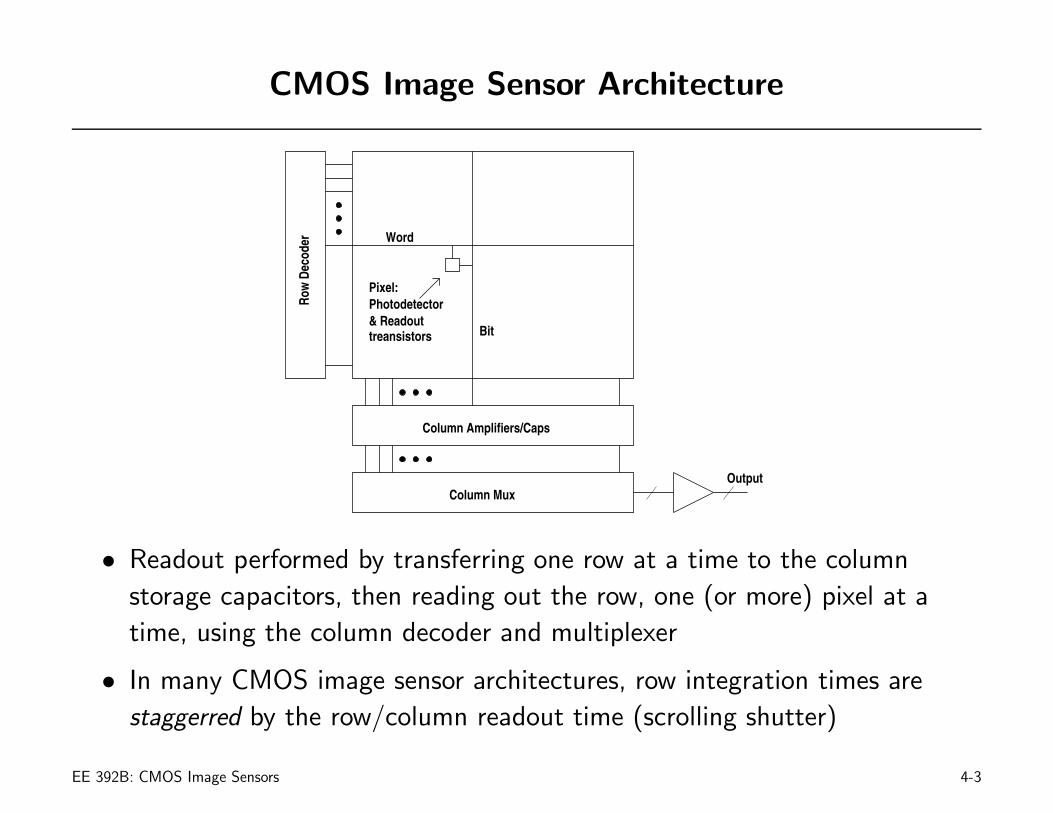
Assuming the static first order MOS transistor model, we obtain
ibias =kn
2·WF
LF
(vGSF − vTF )2,
where WF and LF are the follower transistor width and length, kn is its
transconductance parameter (A/V2), and vTF is its threshold voltage
Thus
vGSF = vTF +
√
2LF
knWF
ibias
Thus the voltage swing is given by
vs = vDD − vTR − vGSF − vbias + vTB
• Remarks:
◦ The available well capacity qQmax = vD ×CD cannot be fully utilized,
since vomin is achieved before the diode voltage drops to ground
◦ The column output voltage is quite nonlinear in illumination (F0)
∗ The collected charge is converted to voltage using the diode
capacitance
∗ The follower nonlinearity due to backgate effect (body tied to
ground) and channel length modulation
EE 392B: CMOS Image Sensors 4-17

• Example: Consider an APS implemented in the 0.5µ CMOS technology
described in Handout 4 with n = 256 rows, vTF = 0.9V, vTR = 1.1V,
vTB = 0.8V, and the parameters shown in the figurePSfrag replacements
WordCb = n × 3fF
Co = 3pF1V16/32
4/2
4/24/2
Reset
3.3V3.3V
vo
Let’s compute the output voltage swing vs. The minimum output voltage
vomin = vbias − vTB = 0.2V
The bias current using kn = 188µA/V2 is ibias = 1.88µA, and the
maximum output voltage is
vomax = vDD − vTR − vGSF = 3.3 − 1.1 − 1.0 = 1.2V
Thus the voltage swing
vs = 1.0V
EE 392B: CMOS Image Sensors 4-18

APS Readout Speed
• Readout time for a row is the sum of the time to transfer the row to the
column capacitors and the time to read out the pixel values via the
column multiplexer (column readout time)
• APS column readout time (and not row transfer time) is the real
performance limiter if the sensor is read out serially (row readout time
becomes the limiting factor for parallel/on-chip readout)
• Let’s find the row transfer time assuming k = 8 bits of resolution for the
example APS
To find the worst case row transfer time, we use the following equivalent
circuit
EE 392B: CMOS Image Sensors 4-19
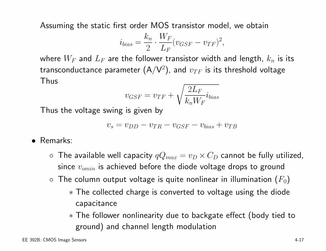
PSfrag replacements
3.3V
3.3V
2.2V
0V
1.88µA
vo
C′
o = (3 + 0.768)pF
follower
Define the row transfer time trow as the time from the access transistor
turning on to the output voltage vo reaching to within half a bit of its
steady state value, i.e.,
vo(trow) ≥ vo(∞) −vs
2k+1
By KCL
1.88 × 10⁻⁶ + C ′o
dvo
dt= 188 × 10−6 × (1.3 − vo)
2
EE 392B: CMOS Image Sensors 4-20

This differential equation can be solved analytically by separation of
variables, and we obtain
trow =C ′
o
2√
knibias
ln
(
(β + ρ)(α − ρ)
(β − ρ)(α + ρ)
)
,
where
ρ =
√
ibias
kn
α = vo(∞) + ρ − vo(0)
β = vo(∞) + ρ − vo(trow)
Using the previous parameter values and assuming k = 8bits, we have
◦ vo(0) = vomin = 0.2V
◦ vo(∞) = vomax = 1.2V
◦ vo(trow) = 1.198V
Substituting, we obtain
trow = 444 ns
EE 392B: CMOS Image Sensors 4-21

APS Readout Speed from HSPICE Simulation
0 0.25 0.5 0.75 1.0 1.25 1.5 0.2
0.3
0.4
0.5
0.6
0.7
0.8
0.9
1.0
1.1
1.2
PSfrag replacementstrow
time (µs)
vo
(V)
EE 392B: CMOS Image Sensors 4-22

Comments on APS Readout Speed
• The row transfer time increases linearly with Cb (same as PPS)
• It decreases with bias current ibias. Reducing bias current also increases
voltage swing and reduces power consumption
• It is considerably shorter than PPS. Our estimate, however, is somewhat
optimistic as you can see from the HSPICE simulations, which gives
around 570ns. This is because we made several simplifying assumptions
including ignoring access transistor resistance, transistor channel
modulation, and assuming quadratic current law. The effects of these
nonidealities are discussed in [Salama’ 03]
• The analysis we performed assumed that the bitline is reset after each row
read. If the bitline is not reset and is allowed to be discharged through the
bias current, the row transfer time becomes dominated by the discharge
time
• PPS can be made as fast as APS by using a faster charge amplifier.
However, readout power consumption becomes much higher than APS
EE 392B: CMOS Image Sensors 4-23

4.1-Mpixel APS Example
• 0.35 µm 2P3M process
• 2352(H)×1728(V) pixels
• 240 Frames/sec
• 7µm × 7µm pixel
• 10 bit column ADC
• Conversion gain: 39 µV/e-
• Sensitivity @550nm: 2.5 V/Lux.sec
Krymski et al. “A High-Speed, 240-Frames/s, 4.1-Mpixel CMOS Sensor,” IEEE Transactions on Electron Devices,
vol. 50, pp. 130-135, January 2003
EE 392B: CMOS Image Sensors 4-24

4.1-Mpixel APS Circuit and Layout
• APS readout circuit sampled and directly converted by per-column
successive approximation ADC
Krymski et al. “A High-Speed, 240-Frames/s, 4.1-Mpixel CMOS Sensor,” IEEE Transactions on Electron Devices,
vol. 50, pp. 130-135, January 2003
EE 392B: CMOS Image Sensors 4-25

CMOS Photogate APS
PSfrag replacements
vDD
vDD
vDD
vX
Reset i
Reset i
Xi
Xi
Pixel(i, j)
P-sub
Dij
n+n+
Word i
Word i
bit j
Gij
Gij
integration
EE 392B: CMOS Image Sensors 4-26

Potential Well Diagram for Photogate APS
PSfrag replacements
G X
vDD
Reset
During integration
During reset
During charge transfer
During readout
EE 392B: CMOS Image Sensors 4-27

Comments on Operation
• Before reading a row
◦ Floating node Dij is reset
◦ To transfer the accumulated charge on the photogate to the floating
node Dij, the transfer gate is turned to an intermediate voltage
vX ≤ vDD2
V and the gate voltage is lowered to 0V (CCD like
operation)
• The transfer gate can also be kept at a constant intermediate voltage
throughout to avoid blooming and to reduce switching noise
• Well capacity is determined by the voltage swing on the floating node and
its capacitance Cd
• Column and chip circuits are identical to photodiode APS and the rest of
readout operation is identical to photodiode APS
• The subcircuit consisting of the transfer gate, reset transistor and follower
transistor is the same as the CCD output amplifier circuit
EE 392B: CMOS Image Sensors 4-28
Advantages and Disadvantages of Photogate
Advantages:
• Conversion gain qCd
is independent of photodetector, can achieve higher
conversion gain than photodiode APS (lower QE, however)
• Cd very useful, can be used for
◦ Providing “snap shot” operation by globally turning on all transfer
gates (readout still performed one row at a time)
◦ Performing true correlated double sampling (CDS)
Disadvantages:
• More devices (larger pixel or lower fill factor than photodiode)
• Lower QE, poor blue response
• Incomplete charge transfer due to the n+ drain of the transfer gate (we
are assuming a standard CMOS process here)
EE 392B: CMOS Image Sensors 4-29

Pinned Diode APS
PSfrag replacementsvDD
vDD
vDD
vX
Reset i
Reset i
Xi
Xi
Pixel(i, j)
P-sub
Dij
n+p+
n
Word i
Word i
bit j
Gij
integration
EE 392B: CMOS Image Sensors 4-30

Comments on Operation
• Operation similar to photogate APS
• Before reading a row
◦ Floating node Dij is reset to vDD
◦ The transfer gate is turned on to transfer the accumulated charge to
the floating node Dij
• “snap-shot” operation can be performed by globally turning on all transfer
gates (readout performed one row at a time)
• Well capacity is determined by the voltage swing on the floating node and
its capacitance Cd
EE 392B: CMOS Image Sensors 4-31

Advantages and Disadvantages of Pinned Photodiode
Advantages:
• Conversion gain qCd
is independent of photodiode capacitance and can be
tailored for application (e.g., low-light sensitivity)
• Allows for true correlated double sampling (CDS)
• High QE in blue range
• Typically much lower dark current than standard nwell/psub diode
• Isolated floating diffusion allows for transistor sharing
Disadvantages:
• Requires significant modifications to standard CMOS process
• Higher reset voltage required for complete transfer
• Larger pixel required unless transistors are shared
EE 392B: CMOS Image Sensors 4-32

1.3-Mpixel Pinned Diode APS Example
• 0.35 µm 1P3M CMOS process
• 1280(H)×1024(V) pixels
• 30 Frames/sec
• 5.6 µm x 5.6 µm pixel
• 11 bit ADC
• Conversion gain: 26 µV/e-
• Sensitivity @550nm: 1.4 V/Lux-sec
Findlater et al. “SXGA Pinned Photodiode CMOS Image Sensor in 0.35µm Technology,” IEEE International
Solid-State Circuits Conference, 12.4, 2003
EE 392B: CMOS Image Sensors 4-33
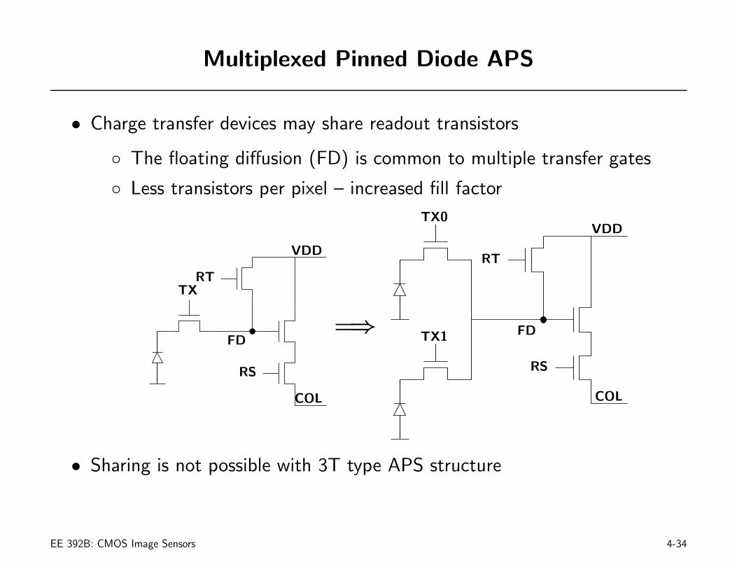
Multiplexed Pinned Diode APS
• Charge transfer devices may share readout transistors
◦ The floating diffusion (FD) is common to multiple transfer gates
◦ Less transistors per pixel – increased fill factor
PSfrag replacements TXRT
RS
FD
VDD
COL
=⇒
PSfrag replacements
RT
RS
FD
VDD
COL
TX0
TX1
• Sharing is not possible with 3T type APS structure
EE 392B: CMOS Image Sensors 4-34
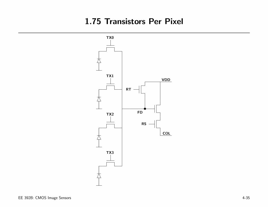
1.75 Transistors Per Pixel
PSfrag replacements
RT
RS
FD
VDD
COL
TX0
TX1
TX2
TX3
EE 392B: CMOS Image Sensors 4-35

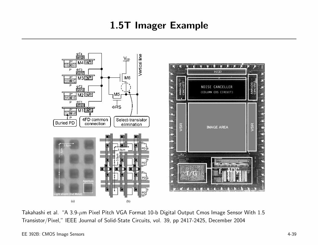
1.75T Imager Example
Mori et al. “1/4-Inch 2-Mpixel MOS Image Sensor With 1.75 Transistors/Pixel,” IEEE Journal of Solid-State
Circuits, vol. 39, pp 2426-2430, December 2004
EE 392B: CMOS Image Sensors 4-36

1.5 Transistors Per Pixel
PSfrag replacements
RS
FD
VDD
COL
TX0
TX1
TX2
TX3
PSfrag replacements
COL(i, j)
RS(k, j)
TX(i, j)
FD(k, j)
rowtime
EE 392B: CMOS Image Sensors 4-37

Comments on Operation
• Operation made possible by the inherent isolation between floating
diffusion and photodiode during integration
• Works through “winner-take-all” nature of source follower:
1. Reset the diffusion by pulling column line high and turning RS on
2. Turn TX on to transfer, then read out
3. Turn TX off, then RS on, while pulling column line low
◦ This sets the floating diffusion low, which disables the source
follower from acting on the column line until next selection
EE 392B: CMOS Image Sensors 4-38
1.5T Imager Example
Takahashi et al. “A 3.9-µm Pixel Pitch VGA Format 10-b Digital Output Cmos Image Sensor With 1.5
Transistor/Pixel,” IEEE Journal of Solid-State Circuits, vol. 39, pp 2417-2425, December 2004
EE 392B: CMOS Image Sensors 4-39

Disadvantages of Multiplexing
• Requires the use of pinned diode (or photogate)
• Longer array readout
• Introduces additional pixel nonuniformity due to layout asymmetry
◦ Less of a problem when color filter array is used (high uniformity
among groups of 2 × 2 pixels)
• More complex row readout operation
EE 392B: CMOS Image Sensors 4-40

Digital Pixel Sensor (DPS)
• An important trend in digital imaging system design is the integration of
CMOS image sensor with analog and digital processing down to the pixel
level
• Such integration saves power and reduces system size
• More interestingly, it provides the ability to rethink the imaging system
architecture
• An important example is where and how to perform the A/D conversion
• DPS integrates an ADC per pixel
EE 392B: CMOS Image Sensors 4-41

ADC Integration Options
PSfrag replacements
Per-pixel (DPS)
Per-columnPer-chip
Row
Deco
der
Column Multiplexer
EE 392B: CMOS Image Sensors 4-42

Per-Level ADC (DPS)
• Each pixel (or group of pixels) has an ADC, all ADCs operate in parallel
• Advantages:
◦ High speed readout due to parallel conversion and digital readout
◦ High signal swing
◦ Eliminates column temporal noise and FPN (more on this later)
◦ Process scalable – low speed ADCs using simple circuits
• Disadvantage:
◦ Large pixel size (existing ADC implementations not feasible)
◦ Limited ADC resolution (because of limited pixel size)
◦ Complexity of implementation
• It is possible to perform A/D conversion with very few transistors per
pixels, and
• Pixel size problem becomes less severe as technology scales
EE 392B: CMOS Image Sensors 4-43

Multi-Channel Bit-Serial (MCBS) ADC [Yang’ 99]
• ADC implements a quantization table
ADC Input Gray Code
0 − 18 0 0 0
18 −
28 0 0 1
28− 3
80 1 1
38− 4
80 1 0
48− 5
81 1 0
58− 6
81 1 1
68− 7
81 0 1
78 − 1 1 0 0
• Key Point: Each output bit can be separately generated (this is how flash
ADC performs the conversion)
EE 392B: CMOS Image Sensors 4-44

How 1-bit Comparator/Latch WorksPSfrag replacements
input1
input2
RAMP
RAMP
BITX
BITX
LSB
S
S
comparatorlatch
OUT
Time
D
G
Q
1
1
1
11
0
0
0
00 0
18
38
58
78
EE 392B: CMOS Image Sensors 4-45

MCBS ADC – Block Diagram
PSfrag replacements
CODE
BITXBITX
RAMP
DAC
channel 1
channel 2
channel n
Controller
analog
analog
analoginput 1
input 2
input n
out 1
out 2
out n
D
D
D
G
G
G
Q
Q
Q
EE 392B: CMOS Image Sensors 4-46

Output Image Format
PSfrag replacements 1
1
11
1
1
12
23
4
0
0
Bit Plane
m
Frame
Next Frame
Time
EE 392B: CMOS Image Sensors 4-47

CCTV DPS Chip [Bidermann’ 04]
• 0.18µm CMOS technology
• 742 × 554 pixel array
• Per pixel-quad MCBS ADC
• 7µ × 7µ pixels
• 5M-bit frame buffer
• Per-column DSP
• Micro-controller
• 500 frames/sec internal
• 60 frames/sec external
• 14-bit dynamic range
EE 392B: CMOS Image Sensors 4-48

Multiplexed MCBS ADC Pixel Circuit [Bidermann’ 04]
EE 392B: CMOS Image Sensors 4-49

Single-Slope Based DPS [Kleinfelder’ 01]
• 0.18µm CMOS technology
• 352 × 288 pixels (CIF)
• 9.4µ × 9.4µ pixels
• 37 transistors/pixel
• 3.8 million transistors
• 8 bit single slope ADC and
memory/ pixel
• 64 wide digital output bus at
167 MHz
• > 10, 000 frames/s continu-
ous imaging
EE 392B: CMOS Image Sensors 4-50

ADC Operation
Input
AnalogRamp
Memory
Gray CodeCounter
8
8
Digital OutComp. Out
Ramp
Input
Comp.Out
MemoryLoading
MemoryLatched
Counter(Gray Code)
LatchedValue
0 1 0
EE 392B: CMOS Image Sensors 4-51

Pixel Schematic
**
*
*
PGTX
Pixel ResetReset V
RampBias 1Bias 2
ReadData I/O
8
Comparator 8-Bit MemorySensor
EE 392B: CMOS Image Sensors 4-52

Summary
• Described several CMOS image sensor architectures:
◦ PPS
◦ Photodiode APS
◦ Photogate APS
◦ Pinned-diode APS
◦ Multiplexed pinned-diode APS
• Discussed their advantages and disadvantages
• Analyzed PPS and APS readout circuit:
◦ Charge to voltage transfer function
◦ Voltage swing
◦ Readout speed
EE 392B: CMOS Image Sensors 4-53

Architecture Comparsion
PPS 3T APS Photogate APS Pinned-diode APS
Transistors/pixel 1 3 1.5–4 1.5–4
QE of blue OK OK Bad Very good
Reset Before readout After readout Before readout Before readout
Shutter Scrolling Scrolling Snap-shot Snap-shot
Transfer function Linearity High Low Low Low
Row transfer time Slow Fast Fast Fast
EE 392B: CMOS Image Sensors 4-54